

Page 1

Model M3460
Ride-Thru
Voltage Regulator
Customer Reference Manual
Page 2

Bonitron, Inc.
2
Bonitron, Inc.
Nashville, TN
An industry leader in providing solutions for AC drives.
ABOUT BONITRON
Bonitron designs and manufactures quality industrial electronics that improve the reliability of
processes and variable frequency drives worldwide. With products in numerous industries, and
an educated and experienced team of engineers, Bonitron has seen thousands of products
engineered since 1962 and welcomes custom applications.
With engineering, production, and testing all in the same facility, Bonitron is able to ensure its
products are of the utmost quality and ready to be applied to your application.
The Bonitron engineering team has the background and expertise necessary to design, develop,
and manufacture the quality industrial electronic systems demanded in today’s market. A strong
academic background supported by continuing education is complemented by many years of
hands-on field experience. A clear advantage Bonitron has over many competitors is combined
on-site engineering labs and manufacturing facilities, which allows the engineering team to have
immediate access to testing and manufacturing. This not only saves time during prototype
development, but also is essential to providing only the highest quality products.
The sales and marketing teams work closely with engineering to provide up-to-date information
and provide remarkable customer support to make sure you receive the best solution for your
application. Thanks to this combination of quality products and superior customer support,
Bonitron has products installed in critical applications worldwide.
Page 3

Bonitron, Inc.
3
AC DRIVE OPTIONS
In 1975, Bonitron began working with AC inverter drive specialists at synthetic fiber plants to
develop speed control systems that could be interfaced with their plant process computers. Ever
since, Bonitron has developed AC drive options that solve application issues associated with
modern AC variable frequency drives and aid in reducing drive faults. Below is a sampling of
Bonitron’s current product offering.
WORLD CLASS PRODUCTS
Undervoltage Solutions
Overvoltage Solutions
Uninterruptible Power for Drives
(DC Bus Ride-Thru)
Voltage Regulators
Chargers and Dischargers
Energy Storage
Braking Transistors
Braking Resistors
Transistor/Resistor Combo
Line Regeneration
Dynamic Braking for Servo Drives
Common Bus Solutions
Portable Maintenance Solutions
Single Phase Power Supplies
3-Phase Power Supplies
Common Bus Diodes
Capacitor Formers
Capacitor Testers
Power Quality Solutions
Green Solutions
12 and 18 Pulse Kits
Line Regeneration
Page 4

M3460
4
1. INTRODUCTION....................................................................................................................7
1.1. Who Should Use This Manual ...................................................................................................... 7
1.2. Purpose and Scope ........................................................................................................................ 7
1.3. Manual Revision ........................................................................................................................... 7
Figure 1-1: M3460R in R11 Chassis and M3460B in R2 Chassis ........................................................... 7
1.4. Symbol Conventions Used in this Manual and on Equipment ..................................................... 8
2. PRODUCT DESCRIPTION ...................................................................................................9
2.1. Related Products and Documents ................................................................................................. 9
2.1.1. Products ............................................................................................................................................ 9
2.1.2. Documents ...................................................................................................................................... 10
2.2. Part Number Breakdown ............................................................................................................ 10
Figure 2-1: Example of Part Number Breakdown .................................................................................. 10
Table 2-1: System Voltage Rating Codes .............................................................................................. 10
Table 2-2: Chassis Size Codes ............................................................................................................... 11
2.3. General Specifications ................................................................................................................ 11
Table 2-3: M3460R General Specifications ........................................................................................... 11
Table 2-4: M3460B General Specifications ........................................................................................... 11
2.4. General Precautions and Safety Warnings ................................................................................. 12
3. INSTALLATION INSTRUCTIONS ...................................................................................13
3.1. Environment ............................................................................................................................... 13
3.2. Unpacking ................................................................................................................................... 13
3.3. Mounting .................................................................................................................................... 13
3.4. Wiring and User Connections ..................................................................................................... 13
3.4.1. Power Wiring ................................ ................................ ................................................................ .. 13
Table 3-1: M3460R Power Wiring Connections .................................................................................... 14
Table 3-2: M3460B Power Wiring Connections .................................................................................... 14
3.4.2. Control Interface and I/O Wiring .................................................................................................... 15
Table 3-3: User I/O Connections with 3460M6 Board .......................................................................... 16
Table 3-4: User I/O Connections with 3660D1 Board ........................................................................... 17
Figure 3-1: M3460 Interconnections with DP10 .................................................................................... 17
3.5. Typical Configurations ............................................................................................................... 18
Figure 3-2: M3460R Typical Configuration without Energy Storage .................................................... 18
Figure 3-3: M3460R Typical Configuration with Electrolytic Capacitor Storage Bank ........................ 19
Figure 3-4: M3460R Typical Configuration with Ultracapacitor Storage Bank .................................... 20
Figure 3-5: M3460B Typical Configuration with Battery Storage Bank ............................................... 21
4. OPERATION .........................................................................................................................23
4.1. Functional Description ............................................................................................................... 23
4.2. M3460R Operation for Full Outage Protection .......................................................................... 23
4.3. Operation Modes and Configuration .......................................................................................... 23
4.3.1. Normal Operation ........................................................................................................................... 23
4.3.2. Test Mode ....................................................................................................................................... 23
4.4. I/O, Features, and Displays ......................................................................................................... 24
Figure 4-1: 3460M6 Status Interface Board Layout ............................................................................... 24
Figure 4-2: 3460C1 Control Board Layout ............................................................................................ 24
Figure 4-3: 3460D5 Power Supply Board Layout (for 380V and 460V) ............................................... 25
Figure 4-4: 3460D6 Power Supply Board Layout (for 575V) ................................................................ 25
4.4.1. Input Terminals – 3460M6 TB7 ..................................................................................................... 25
Table 4-1: 3460M6 Enable Input Logic Jumper Details ........................................................................ 26
4.4.2. Output Terminals - 3460M6 TB5, TB6 .......................................................................................... 26
Table 4-2: 3460M6 Status Output Signal Logic Jumper Details ............................................................ 28
Page 5

Table of Contents
5
4.4.3. Local I/O Power Supply - TB6 - 1, 9 .............................................................................................. 28
4.4.4. Run Timeout Selection .................................................................................................................... 28
Table 4-3: Run Timeout Jumper Configurations .................................................................................... 28
4.4.5. Test Timer Selection ....................................................................................................................... 29
Table 4-4: Test Timer Jumper Configurations ....................................................................................... 29
4.4.6. Indicators......................................................................................................................................... 29
4.4.7. Fan Timer ........................................................................................................................................ 30
4.4.8. Display Options .............................................................................................................................. 30
Table 4-5: Display Panel Configurations ............................................................................................... 30
Figure 4-5: Display Panels ..................................................................................................................... 30
4.5. DC Bus Threshold Voltage Setting ............................................................................................ 32
4.5.1. Determining the DC Bus Threshold Voltage Setting Directly (M3460R Models) ......................... 32
4.5.2. Determining the DC Bus Threshold Voltage Setting Directly (M3460B Models) ......................... 33
4.5.3. Determining the DC Bus Threshold Voltage Setting Using the Test Mode .................................... 33
4.5.4. Adjusting the DC Bus Threshold Voltage Setting .......................................................................... 34
4.6. Input Undervoltage (IUV) Level Adjustment ............................................................................. 34
4.7. Output Undervoltage Level Adjustment ..................................................................................... 34
5. START-UP, MAINTENANCE AND TROUBLESHOOTING .........................................35
5.1. M3460R Start-up / Field Test Procedure .................................................................................... 35
5.2. M3460B Start-up / Field Test Procedure .................................................................................... 36
5.3. Maintenance Items ...................................................................................................................... 37
5.3.1. Capacitor Replacement Recommendations ..................................................................................... 37
5.3.2. Capacitor Testing Procedure ........................................................................................................... 38
5.3.3. Cleaning .......................................................................................................................................... 38
5.3.4. Fans ................................................................................................................................................. 38
5.3.5. Heatsinks ......................................................................................................................................... 38
5.4. Troubleshooting .......................................................................................................................... 39
Table 5-1: Troubleshooting Guide ......................................................................................................... 39
5.5. Technical Help – Before You Call ............................................................................................. 40
6. ENGINEERING DATA ........................................................................................................41
6.1. Ratings ........................................................................................................................................ 41
Table 6-1: M3460 kW Ratings ............................................................................................................... 41
Table 6-2: Factory Setpoints for DC Bus Threshold and Test Boost Voltages ...................................... 41
Table 6-3: M3460R Minimum Input Voltages ....................................................................................... 41
Table 6-4: M3460B Battery Bank Typical Values ................................................................................. 41
Table 6-5: M3460R Model Specifications for 230 – 480 VAC Systems ............................................... 42
Table 6-6: M3460B Model Specifications for 230 – 480 VAC Systems ............................................... 42
Table 6-7: M3460R Model Specifications for 575 - 600 VAC Systems ................................................ 43
Table 6-8: M3460B Model Specifications for 575 - 600 VAC Systems ................................................ 43
6.2. Efficiency / Power Consumption ................................................................................................ 43
6.3. Certifications .............................................................................................................................. 44
6.3.1. Underwriters Laboratories Listing .................................................................................................. 44
6.3.2. CE Conformity ................................................................................................................................ 44
6.3.3. Third Party Certifications ................................................................................................................ 44
6.4. Branch Circuit Protection and Wire Sizing ................................................................................ 44
Table 6-9: M3460R Input Power Wiring Sizes and Fusing ................................................................... 45
Table 6-10: M3460B Input Power Wiring Sizes and Fusing ................................................................. 45
6.5. Dimensions and Mechanical Drawings ...................................................................................... 46
Figure 6-1: M3460-R10 Chassis Dimensional Outline .......................................................................... 46
Figure 6-2: M3460-R9 Chassis Dimensional Outline ............................................................................ 47
Figure 6-3: M3460-R11 Chassis Dimensional Outline .......................................................................... 48
Figure 6-4: M3460-R2 Chassis Dimensional Outline ............................................................................ 49
Figure 6-5: DD5 Digital Display Cutout and Mounting Dimensions ..................................................... 50
Page 6

M3460
6
Figure 6-6: DP10 Display Cutout and Mounting Dimensions ............................................................... 50
7. APPENDICES ........................................................................................................................51
7.1. M3460 Installation Considerations ............................................................................................. 51
7.2. Specifying an Ultracapacitor Storage Bank for Full Outage Protection With M3460R Models 51
7.2.1. Energy Required for Outage ........................................................................................................... 53
7.2.2. Minimum Capacitor Bank Voltage ................................................................................................. 53
7.2.3. Peak Current .................................................................................................................................... 53
7.2.4. Capacitor Specifications ................................................................................................................. 53
7.2.5. Minimum Series String ................................................................................................................... 54
7.2.6. Available Joules .............................................................................................................................. 54
7.3. Steering Diode Sharing with a Bonitron M3460 Ride-Thru ....................................................... 55
Figure 7-1: Diode Sharing Example ....................................................................................................... 56
7.4. Sag Only Installations & Circulating Currents ........................................................................... 57
Figure 7-2: M3460R Typical Configuration without Energy Storage .................................................... 57
Figure 7-3: M3460R Typical Configuration with Current Flow ............................................................ 58
Figure 7-3: M3460R Typical Configuration with Current Flow with affected SCR Highlighted .......... 59
Figure 7-4: M3460R Typical Configuration with Ultracapacitor Storage Bank .................................... 60
Page 7
User’s Manual
7
1. INTRODUCTION
1.1. WHO SHOULD USE THIS MANUAL
This manual is intended for use by anyone who is responsible for integrating, installing,
maintaining, troubleshooting, or using this equipment with any AC drive system.
Please keep this manual for future reference.
1.2. PURPOSE AND SCOPE
This manual is a user’s guide for the model M3460 ride-thru voltage regulator. It will
provide the user with the necessary information to successfully install, integrate, and
use this in a variable frequency AC drive system.
In the event of any conflict between this document and any publication and/or
documentation related to the AC drive system, the latter shall have precedence.
1.3. MANUAL REVISION
Figures 3-2, 3-3, 3-4, and 3-5 were updated in Rev 00d.
Manual template was updated in Rev 00e
Section 7.4 Application Note for Circulation Currents was added in Rev 00f.
Figure 6-5 was updated in Rev 00g
Updates to Section 5.4 and 7.2, and Figure 3-4 were made in Rev 00h.
The display options were updated in Rev 00i.
Updated tables 2-3, 2-4, 6-1, 6-2, 6-3, 6-4 and figures 6-1, 6-2, 6-3 in Rev 00j.
Update to include DD5 display in Rev 01a.
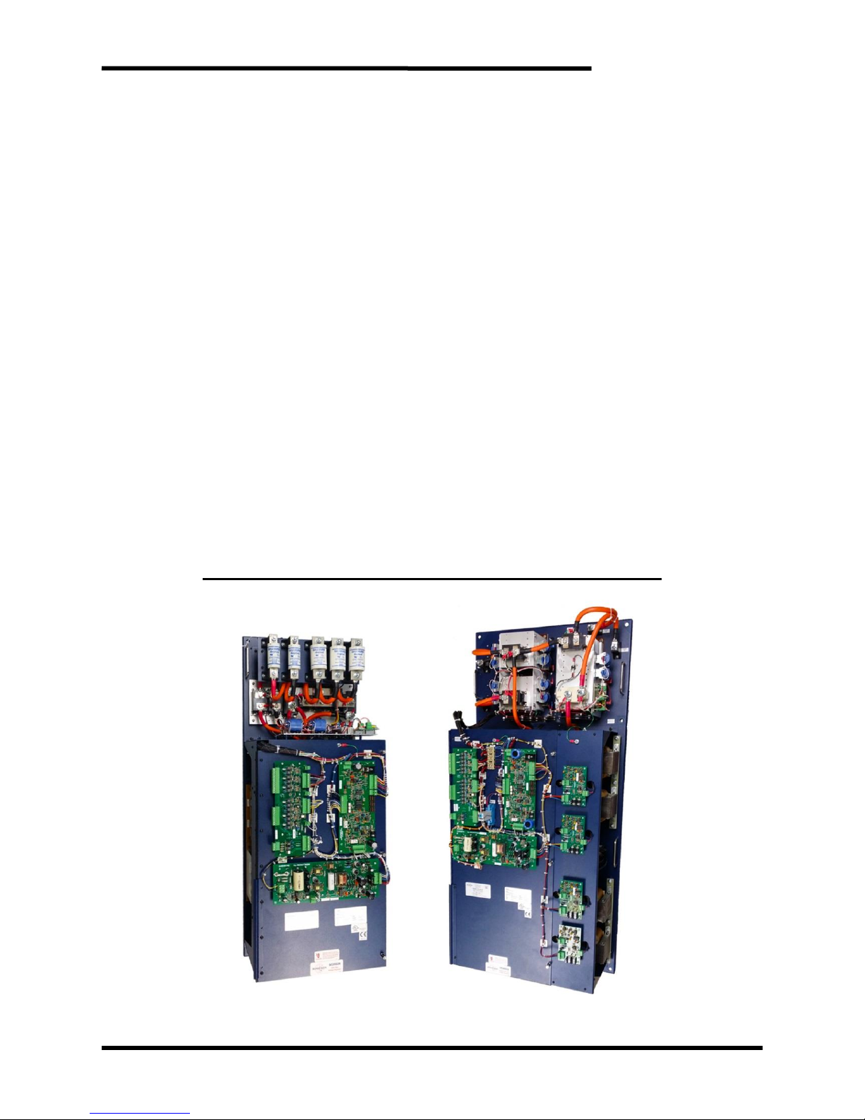
Figure 1-1: M3460R in R11 Chassis and M3460B in R2 Chassis
Page 8
M3460
8
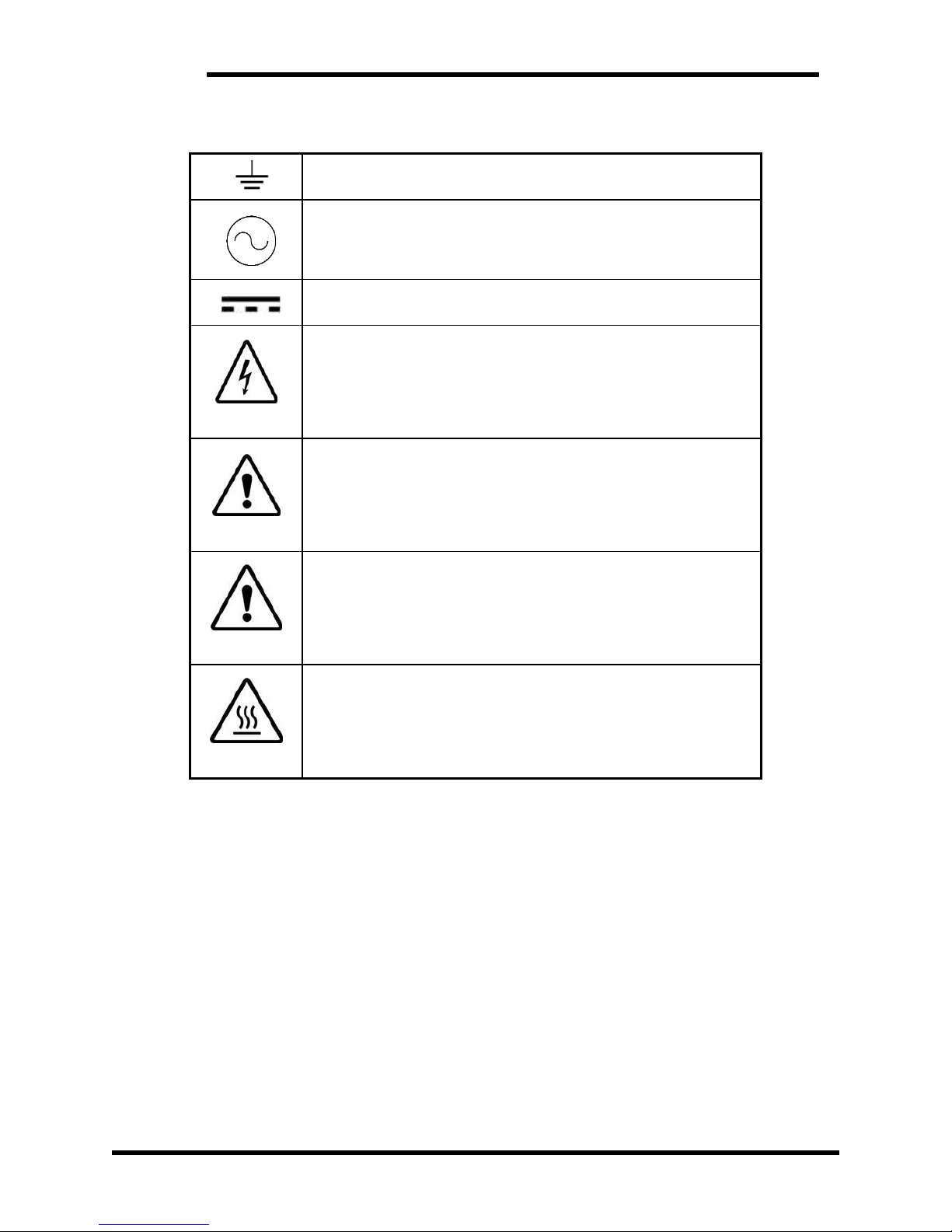
1.4. SYMBOL CONVENTIONS USED IN THIS MANUAL AND ON EQUIPMENT
Earth Ground or Protective Earth
AC Voltage
DC Voltage
DANGER!
DANGER: Electrical hazard - Identifies a statement that indicates
a shock or electrocution hazard that must be avoided.
DANGER!
DANGER: Identifies information about practices or circumstances
that can lead to personal injury or death, property damage, or
economic loss.
CAUTION!
CAUTION: Identifies information about practices or circumstances
that can lead to property damage, or economic loss. Attentions
help you identify a potential hazard, avoid a hazard, and
recognize the consequences.
CAUTION!
CAUTION: Heat or burn hazard - Identifies a statement regarding
heat production or a burn hazard that should be avoided.
Page 9

User’s Manual
9
2. PRODUCT DESCRIPTION
Bonitron’s M3460 ride-thru voltage regulators provide protection from power quality events
for variable frequency drives (VFDs) that use a fixed rectifier and DC bus. The M3460R
provides sag protection for up to 2 seconds at 50% line sag on all 3 phases. It can also
provide protection from short term full outages of up to 2 seconds with the addition of
storage systems, such as capacitors. The M3460B, in conjunction with a battery bank,
provides full outage protection for up to 4 minutes at full power rating or 15 minutes at
50% power rating during a full outage.
Industries with continuous processes can suffer huge losses from equipment downtime,
loss of production, or damaged product when VFDs trip on under-voltage conditions.
Traditional UPS solutions are connected in series, which decreases the overall drive
system reliability. All Bonitron ride-thru products connect in parallel with the drive, thus
increasing system availability and reliability.
The M3460 regulates incoming voltage to the DC bus of the variable frequency drive. This
allows the drive to “ride through” these events while maintaining motor speed and torque
without experiencing drive shutdown.
ADVANTAGES
• Reliability
• Parallel connection to AC system
• M3460 maintenance can be done while normal process is on-line
• Works with almost any fixed bus, variable frequency, PWM drive
• Only 2-3 parallel connections
• Can use existing AC feed wiring and breakers
• Instant response
• Bumpless transfer
• Easy commissioning
2.1. RELATED PRODUCTS AND DOCUMENTS
2.1.1. PRODUCTS
S3460CR SERIES RIDE-THRU SYSTEMS
Complete systems that use electrolytic capacitor storage for short term power
outages.
S3460UR SERIES RIDE-THRU SYSTEMS
Complete systems that use ultracapacitor storage for short term power
outages.
S3460BR SERIES RIDE-THRU SYSTEMS
Complete systems that use batteries for longer term power outages.
M3534 SERIES RIDE-THRU MODULES
Voltage regulators used for sag or outage protection of lower power systems.
M3528 BATTERY AND ULTRACAPACITOR CHARGERS
Chargers for high voltage storage strings.
Page 10
M3460
10
2.1.2. DOCUMENTS
Please refer to the KIT 3660DD5 manual when this unit is equipped with the
DD5 Digital Display option. This manual is available at www.bonitron.com or
by contacting Bonitron.
2.2. PART NUMBER BREAKDOWN
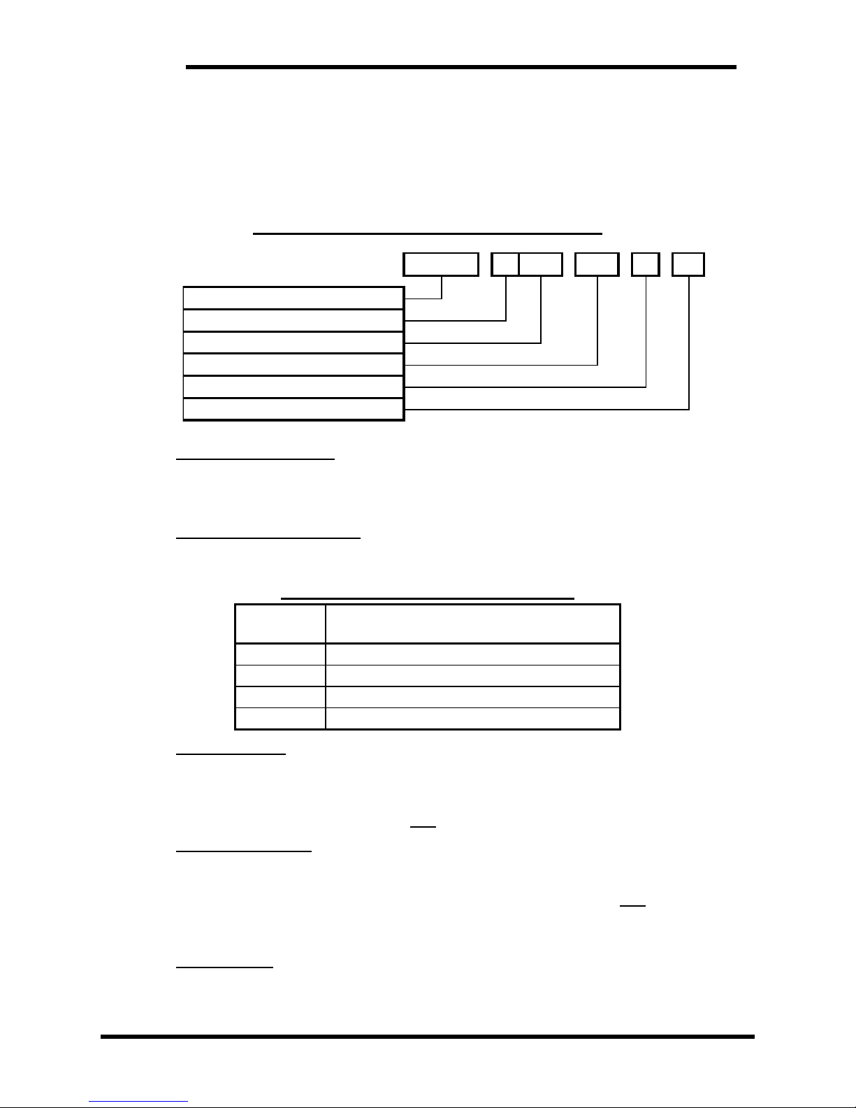
Figure 2-1: Example of Part Number Breakdown
- - - -
F
Fusing
System Voltage Rating
Power Rating
Outage Duration
Chassis Size
M3460R
H
100
240
R9
Base Model Number
BASE MODEL NUMBER
The base model number for all ride-thru modules in this series rated for 2 second
operation is M3460R. The base model number for all ride-thru modules in this series
rated for 4-15 minute operation is M3460B.
SYSTEM VOLTAGE RATING
The M3460 is available in several input voltage ratings. This rating is indicated by a
code as shown in Table 2-1.
Table 2-1: System Voltage Rating Codes
RATING
CODE
NOMINAL VOLTAGE
(AC LINE / DRIVE BUS)
L
230 VAC / 325 VDC
E
380 - 415 VAC / 540 - 585 VDC
H
460 VAC / 650 VDC
C
575 - 600 VAC / 810VDC
POWER RATING
The power rating indicates the maximum power in kilowatts that can safely be handled
by the M3460 and is represented by a 3-digit value based on the nominal DC system
voltage rating and the maximum output current rating of the M3460. For instance, the
rating code for a 100kW M3460 is 100.
OUTAGE DURATION
The outage duration indicates the amount of time (in seconds) the M3460B module is
able to hold the DC bus at the threshold level while loaded to the rated current. This
duration is directly represented by a 3-digit value. For example, 240 in this position,
represents 240 seconds (4 minutes) of outage duration.
This code is omitted on M3460R models.
CHASSIS SIZE
Four open-backplate chassis sizes are indicated by a code as shown in Table 2-2.
This chassis size is determined by the current rating of the unit.
Page 11
User’s Manual
11
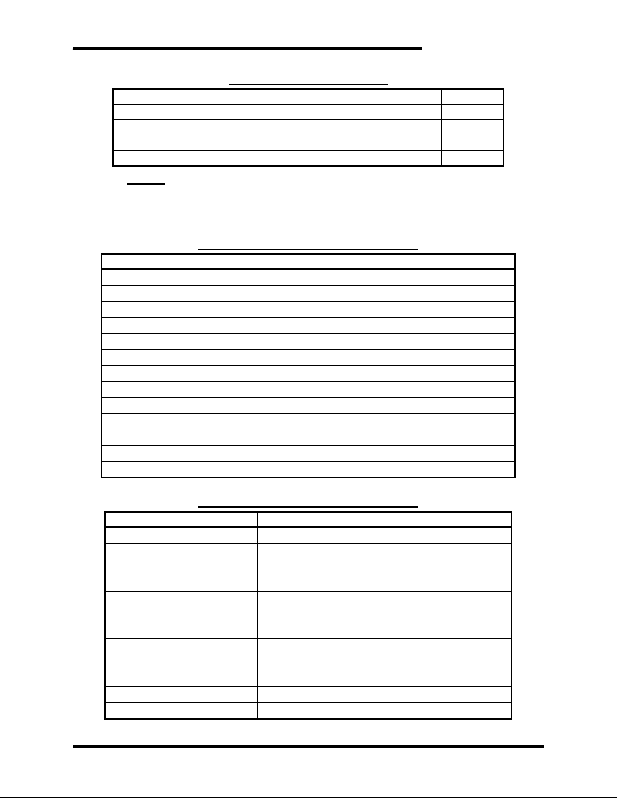
Table 2-2: Chassis Size Codes
CHASSIS SIZE CODE
DIMENSIONS (H X W X D)
3460R
3460B
R10
28.00” x 16.00” x 13.50”
85-127 A
85 A
R9
34.00” x 16.00” x 13.50”
170 A
127-170 A
R11
44.00” x 15.25” x 13.50”
255-425 A - R2
52.00” x 24.00” x 12.50”
-
255-340 A
FUSING
The M3460R comes with internal fusing. This code is omitted on all M3460B models
and M3460R models if internal fusing is not desired.
2.3. GENERAL SPECIFICATIONS
Table 2-3: M3460R General Specifications
PARAMETER
SPECIFICATION
Input AC Voltage
208 – 575 VAC
Input DC Voltage
200 – 675 VDC
Output DC Voltage
265 – 810 VDC
DC Bus Current Rating
85 – 425 ADC
Power Rating
25 – 305 kW
Inactive Power Consumption
<200W
Duty Cycle (Full Load)
1%
Sag/Outage Duration
2 seconds
Enclosure Rating
Open
Operating Temperature
0 to +40ºC
Storage Temperature
-20 to +65 ºC
Humidity
Below 90% non-condensing
Atmosphere
Free of corrosive gas and conductive dust
Table 2-4: M3460B General Specifications
PARAMETER
SPECIFICATION
Input DC Voltage
200 – 675 VDC
Output DC Voltage
265 – 810 VDC
DC Bus Current Rating
85– 340 ADC
Power Rating
25 – 245 kW
Inactive Power Consumption
<200W
Duty Cycle (Full Load)
1%
Sag/Outage Duration
4 minutes at full power or 15 minutes at 50% power
Enclosure Rating
Open
Operating Temperature
0 to +40ºC
Storage Temperature
-20 to+ 65 ºC
Humidity
Below 90% non-condensing
Atmosphere
Free of corrosive gas and conductive dust
Page 12
M3460
12
2.4. GENERAL PRECAUTIONS AND SAFETY WARNINGS
DANGER!
• HIGH VOLTAGES MAY BE PRESENT!
• NEVER ATTEMPT TO OPERATE THIS PRODUCT WITH THE
ENCLOSURE COVER REMOVED!
• NEVER ATTEMPT TO SERVICE THIS PRODUCT WITHOUT FIRST
DISCONNECTING POWER TO AND FROM THE UNIT.
• ALWAYS ALLOW ADEQUATE TIME FOR RESIDUAL VOLTAGES TO
DRAIN BEFORE OPENING THE ENCLOSURE.
• FAILURE TO HEED THESE WARNINGS MAY RESULT IN
SERIOUS INJURY OR DEATH!
CAUTION!
• CERTAIN COMPONENTS WITHIN THIS PRODUCT MAY GET HOT
DURING OPERATION.
• ALWAYS ALLOW AMPLE TIME FOR THE UNIT TO COOL BEFORE
ATTEMPTING SERVICE ON THIS PRODUCT.
• INSTALLATION AND/OR REMOVAL OF THIS PRODUCT SHOULD
ONLY BE ACCOMPLISHED BY A QUALIFIED ELECTRICIAN IN
ACCORDANCE WITH NATIONAL ELECTRICAL CODE OR
EQUIVALENT REGULATIONS.
• BE FO R E A TT EM PTI NG IN S TA LL AT I ON OR RE MO VAL OF
TH IS P RO D UC T, BE SUR E T O REVI EW A LL S YS T EM
DO CU ME N TA TI ON FO R PE R TI NE N T SA FE T Y
PR EC AU TIO NS .
• NO US ER -S E RV IC EA BL E P AR TS AR E C ON TA IN E D
WI TH I N TH I S PR O DU CT . IN OP ER AB LE UN IT S SHOU LD BE
RE PL AC E D OR R E TU RN E D F OR R EP A IR .
• THIS PRODUCT DOES NOT PROVIDE MOTOR OVERLOAD
PROTECTION.
ANY QUESTIONS AS TO APPLICATION, INSTALLATION, OR SERVICE
SAFETY SHOULD BE DIRECTED TO THE EQUIPMENT SUPPLIER.
Page 13
User’s Manual
13
3. INSTALLATION INSTRUCTIONS
The M3460 has an open frame construction. It is intended to be part of a larger variable
frequency drive system, and will require different hardware for interconnection based on
the installation. An appropriate enclosure may need to be provided to protect personnel
from contact and the system from damage. The enclosure may also need to protect the
equipment from the installation environment.
Please read this manual completely before designing the drive system or enclosure layout
to ensure all required elements are included.
3.1. ENVIRONMENT
The maximum ambient operating temperature of the M3460 should not exceed 40C.
Temperatures above this can cause overheating during operation.
The standby heat production of the M3460 is quite low, but can generate significant
heat during boosting. This is only of concern with the M3460B models because the
M3460R run time of 2 seconds will not allow the system to reach thermal equilibrium,
and should not cause thermal issues.
Non-condensing, filtered air may be required to cool the system if other components
cause excessive heat buildup in the enclosure.
3.2. UNPACKING
Inspect the shipping crate and M3460 for damage.
Notify the shipping carrier if damage is found.
3.3. MOUNTING
Mounting dimensions can be found in Section 6.5.
1. Lift M3460 backplate off the crate bottom using the 4 handles. Eyebolts
may be installed in the mounting holes for lifting with hooks or chains.
2. Install the module to the backplate. Secure the M3460 backplate to the
rack using the backplate’s ½” diameter mounting holes. Mounting
hardware is not supplied with the M3460. The power input terminals will
be at the top of the installation.
3. If supplied, install the display panel in an appropriate location.
3.4. WIRING AND USER CONNECTIONS
Review this entire section before attempting to wire the M3460.
3.4.1. POWER WIRING
DANGER!
THE M3460 CAN HAVE MULTIPLE POWER SOURCES, INCLUDING THE MAIN AC INPUT,
ENERGY STORAGE SYSTEMS AND THE DC CONNECTION TO THE VFD.
ENSURE THAT ALL SOURCES ARE DISCONNECTED AND LOCKED OUT BEFORE
ATTEMPTING SERVICE OR INSTALLATION.
FAILURE TO HEED THESE WARNINGS MAY RESULT IN SERIOUS INJURY
OR DEATH!
This section provides information pertaining to the field wiring connections of
the M3460. Actual connection points and terminal numbers of the AC drive
system will be found in the documentation provided with the drive system.
Be sure to review all pertinent AC drive system documentation as well as the
connection details listed below before proceeding.
Page 14
M3460
14
Table 3-1: M3460R Power Wiring Connections
TERMINAL
DESIGNATION
FUNCTION
WIRING
SPECIFICATION
CONNECTION
TORQUE
AC Line
L1, L2, L3
AC Input
600 VAC
3/8" stud
150 lb-in
Storage Bus
+ -
DC Input
600 VAC
Existing
Diode / SCR
Check Device
Datasheet
Drive Bus
+ -
DC Output
600 VAC
3/8" stud
150 lb-in
Ground
600 VAC
5/16" stud
75 lb-in
Table 3-2: M3460B Power Wiring Connections
TERMINAL
DESIGNATION
FUNCTION
WIRING
SPECIFICATION
CONNECTION
TORQUE
Storage Bus
+ -
DC Input
600 VAC
3/8" stud
150 lb-in
Drive Bus
+ -
DC Output
600 VAC
3/8" stud
150 lb-in
Ground
600 VAC
5/16" stud
75 lb-in
Main power connections should be made with copper wire; use compression
fitting lugs. Wire sizing should be appropriate for the current being carried.
System ratings are listed in Section 6.1.
M3460 ride-thru units only provide full currents for a limited amount of time.
Therefore, wire heating is not as much a concern as mechanical strength.
3.4.1.1. AC LINE (L1, L2, L3) CONNECTIONS
The AC input to the M3460R can temporarily reach up to 200% of the
normal input current during a power quality event. Size the upstream
current protection devices accordingly, so that the incoming AC will not
be interrupted by the temporary power draw.
During a power quality event, the AC input to the drive will not be drawing
current. Sizing the incoming AC feed to supply both the drive and the
M3460R simultaneously is not necessary. Even though the input current
during a power quality event may be higher than the normal input current,
this temporary overload is allowed by most codes without upsizing the
normal AC feed bus.
Due to the increased currents in the AC feed during a power quality event,
the total voltage drop of the incoming AC feed should be considered to
make sure the voltage doesn't dip too low.
If line chokes are to be used in the system, the M3460R must be installed
on the load side of these chokes. This minimizes the possibility of
circulating currents through the M3460R and converter section of the
VFD.
There is no need to connect the AC line to the M3460R if an ultracapacitor
bank is being used. The DC connections from the ultracapacitor bank can
be made to any two of the AC line connections so that the existing fuses
Page 15
User’s Manual
15
can be used for protection. Please note that one terminal will not be
connected. See Figure 3-4.
3.4.1.2. STORAGE BUS (+ -) CONNECTIONS
If an electrolytic capacitor bank is used with the M3460R, the input can
be attached directly to the diode bus bars marked Storage Bus. External
fusing between the capacitor bank and the M3460R is recommended.
The M3460B battery bank connections are made at the Storage Bus
terminal blocks at the top of the module.
Make sure the polarity is correct for these connections, as failure to do
so can cause severe damage to the system.
DANGER!
FOR SYSTEMS THAT HAVE DC STORAGE, ALWAYS MEASURE DC VOLTAGES AND
FOLLOW PROPER PRECAUTIONS TO ENSURE THEY ARE AT SAFE LEVELS BEFORE
MAKING CONNECTIONS.
3.4.1.3. DRIVE BUS (+ -) CONNECTIONS
The M3460 must have a DC bus connection directly to the DC bus filter
capacitors within the drives. Connections cannot be made through the
braking terminals or with precharge resistors or DC link chokes between
the output of the M3460 and the DC bus capacitors in the drive. Consult
the manufacturers' documentation or contact Bonitron for further
assistance.
Make sure the polarity is correct for these connections, as failure to do
so can cause severe damage to the system.
DANGER!
FOR SYSTEMS THAT HAVE DC STORAGE, ALWAYS MEASURE DC VOLTAGES AND
FOLLOW PROPER PRECAUTIONS TO ENSURE THEY ARE AT SAFE LEVELS BEFORE
MAKING CONNECTIONS.
3.4.1.4. GROUNDING REQUIREMENTS
All units come equipped with a ground stud that is connected to the
module chassis. Ground the chassis in accordance with local codes.
Typically, the wire gauge will be the same as is used to ground the
attached drive.
3.4.2. CONTROL INTERFACE AND I/O WIRING
Control wiring allows for remote enabling, testing, and monitoring of the
M3460. Some I/O is duplicated to allow for isolated monitoring; some have a
mutual common.
When a display system is used, the system status outputs on 3460M6 TB6 are
connected to the display. This leaves the outputs on 3460M6 TB5 available for
remote monitoring.
Page 16
M3460
16
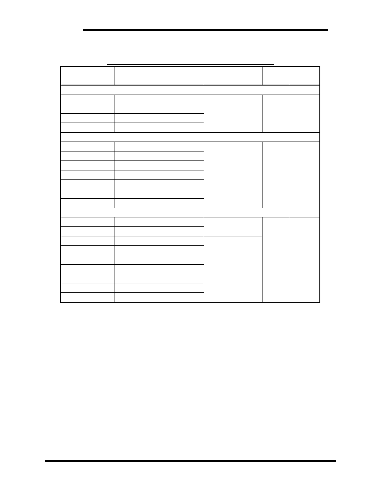
3.4.2.1. CONNECTIONS FOR BASE CONFIGURATION
Table 3-3: User I/O Connections with 3460M6 Board
3460M6
TERMINAL
FUNCTION
ELECTRICAL
SPECIFICATIONS
WIRE
AWG
TORQUE
INPUTS
TB7 – 1
Enable/Disable Input +
24VDC, 20mA
16-12
4.5 lb-in
TB7 – 2
Enable/Disable Input -
TB7 – 3
Test Input +
TB7 – 4
Test Input -
ISOLATED OUTPUTS
TB5 – 1 & 2
Ride-Thru Ready (RTR)
250V / 120mA
16-12
4.5 lb-in
TB5 – 3 & 4
Overtemperature (OT)
TB5 – 5 & 6
Voltage Fault (VF)
TB5 – 7 & 8
Fault (FLT)
TB5 – 9 & 10
Precharge Complete (PCC)
TB5 – 11 & 12
Ride-Thru Active (RTA)
TB5 – 13 & 14
Input Undervoltage (IUV)
COMMON OUTPUTS
TB6 – 1
Local I/O Supply +
24 VDC, 500 mA
16-12
4.5 lb-in
TB6 – 9
Local I/O Supply -
TB6 – 2
Precharge Complete (PCC)
250 V / 120 mA
TB6 – 3
Voltage Fault (VF)
TB6 – 4
Overtemperature (OT)
TB6 – 5
Ride-Thru Ready (RTR)
TB6 – 6
Ride-Thru Active (RTA)
TB6 – 7
Input Undervoltage (IUV)
TB6 – 8
Output Common
3.4.2.2. CONNECTIONS WITH DD5 DIGITAL DISPLAY
When the KIT 3660DD5 digital display is used, some user connections to
the digital display interface are made on a different module than the
M3460. They are made to the 3660I4 interface module.
Refer to the KIT 3660DD5 manual for operational and functional details.
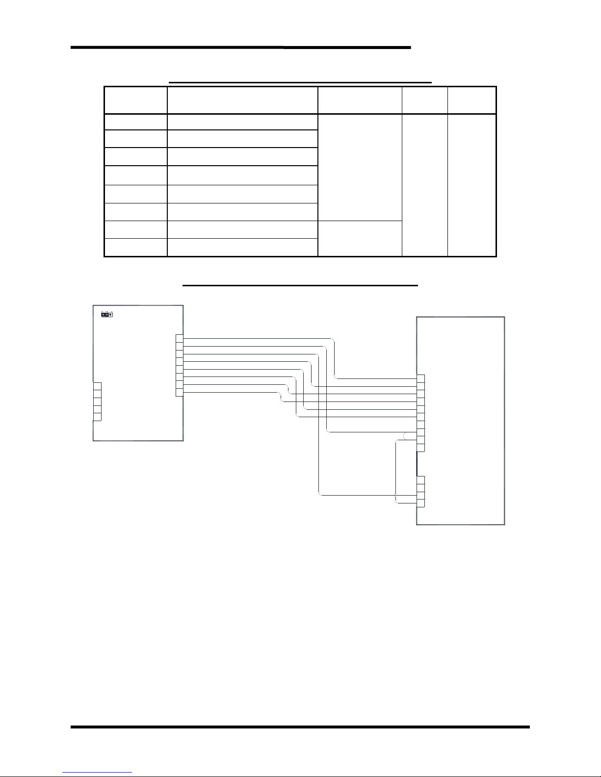
3.4.2.3. CONNECTIONS WITH DP10 ANALOG DISPLAY
When the M3460 is used with the DP10 analog display, the
interconnections are made through TB6 and TB7 on the 3460M6 board
and TB1 on the 3660D1 board.
Page 17
User’s Manual
17
Table 3-4: User I/O Connections with 3660D1 Board
3660D1
TERMINAL
FUNCTION
ELECTRICAL
SPECIFICATIONS
WIRE
AWG
TORQUE
TB1 – 1
Overtemperature (OT)
15 VDC, 15 mA
16
2.1 lb-in
TB1 – 2
Voltage Fault (VF)
TB1 – 3
Ride-Thru Active (RTA)
TB1 – 4
Ride-Thru Ready (RTR)
TB1 – 5
Pre-Charge Complete (PCC)
TB1 – 6
Test
TB1 – 7
Local I/O Supply -
15 VDC, 50 mA
TB1 – 8
Local I/O Supply +
Figure 3-1: M3460 Interconnections with DP10
3660D1
J1
BA
TB4
V+
TB1
3460M6
8
7
6
5
4
3
2
1
COM
TEST
PCC
RTR
RTA
VF
OT
12345678
TB6
910
1234
TB7
1
2
3
4
5
24V+
PCC
VF
OT
RTR
RTA
SIG COM
24V COM
+-+-
Page 18
M3460
18
3.5. TYPICAL CONFIGURATIONS
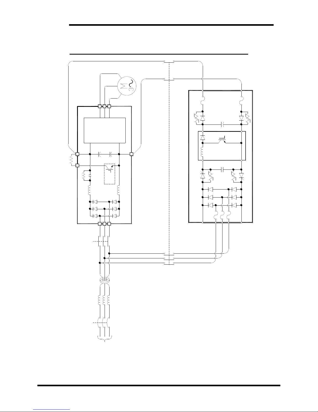
Figure 3-2: M3460R Typical Configuration without Energy Storage
FROM THE SAME FEED TRANSFORMER.
CONNECTED DOWNSTREAM.
2. IF LINE CHOKES ARE USED, RIDE-THRU MUST BE
1. INVERTER AND RIDE-THRU SHOULD BE POWERED
~NOTES~
CHOPPER
BRAKING
INTERNAL
VFD
INVERTER
BRAKING
RESISTOR
DISCONNECT
DRIVE
FEED
AC
CHOKES
LINE
GROUND
FAULT
SENSING
DISCONNECT
RIDE-THRU
M3460R
CHOPPER
+
-
+
-
DRIVE
BUS
STORAGE BUS
STORAGE BUS
Page 19
User’s Manual
19
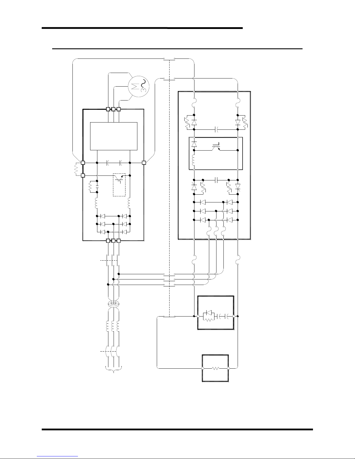
Figure 3-3: M3460R Typical Configuration with Electrolytic Capacitor Storage Bank
FROM THE SAME FEED TRANSFORMER.
CONNECTED DOWNSTREAM.
2. IF LINE CHOKES ARE USED, RIDE-THRU MUST BE
1. INVERTER AND RIDE-THRU SHOULD BE POWERED
~NOTES~
CHOPPER
BRAKING
INTERNAL
VFD
INVERTER
BRAKING
RESISTOR
DISCONNECT
DRIVE
FEED
AC
CHOKES
LINE
GROUND
FAULT
SENSING
DISCONNECT
RIDE-THRU
M3460R
CHOPPER
+
-
+
-
DRIVE
BUS
STORAGE BUS
STORAGE BUS
RESISTOR
DISCHARGE
ELECTROLYTIC
CAPACITORS
WITH PRECHARGE
ASM 3534EC
Page 20
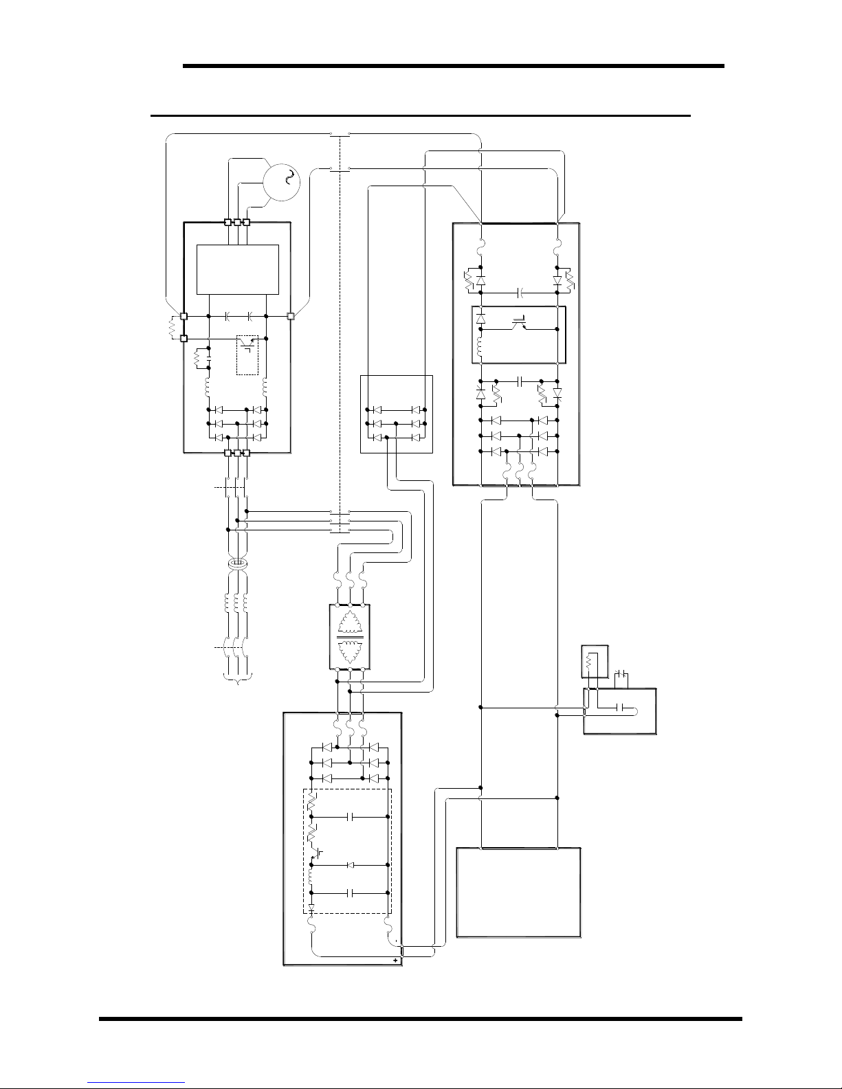
M3460
20
Figure 3-4: M3460R Typical Configuration with Ultracapacitor Storage Bank
KIT 3628T
DISCHARGER
M3628R
CHOPPER
BRAKING
INTERNAL
VFD
INVERTER
BRAKING
RESISTOR
DISCONNECT
DRIVE
FEED
AC
CHOKES
LINE
GROUND
FAULT
SENSING
M3528AC CHARGER
ULTRA CAP
ENERGY STORAGE
BANK
DISCONNECT
RIDE-THRU
M3460R
CHOPPER
+
-
+
-
+
-
DRIVE
RIDE-THRU
DISCONNECT
AUX. CONTACT
BUS
STORAGE BUS
STORAGE BUS
M
3
ISOLATION TRANSFORMER
FROM THE SAME FEED TRANSFORMER.
CONNECTED DOWNSTREAM.
2. IF LINE CHOKES ARE USED, RIDE-THRU MUST BE
1. INVERTER AND RIDE-THRU SHOULD BE POWERED
~NOTES~
+
-
L1
L2
ASM 3460PS
IS LOWER THAN PCC VOLTAGE.
3. ASM 3460 PS WILL BE USED IF THE INPUT DC LEVEL
*OPTIONAL: SEE SECTION 7.2
Page 21
User’s Manual
21
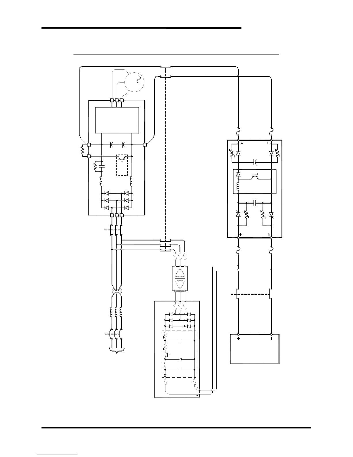
Figure 3-5: M3460B Typical Configuration with Battery Storage Bank
DISCONNECT
DRIVE
DRIVE
FEED
AC
BANK
STORAGE
BATTERY
ENERGY
3460B
CHOPPER
CHOKES
LINE
CHOPPER
BRAKING
INTERNAL
VFD
INVERTER
BRAKING
RESISTOR
GROUND
FAULT
SENSING
DISCONNECT
BATTERY
RIDE-THRU
DISCONNECT
BUS
M
3
STORAGE
BUS
M3528AC CHARGER
ISOLATION TRANSFORMER
Page 22

M3460
22
This page intentionally left blank
Page 23

User’s Manual
23
4. OPERATION
4.1. FUNCTIONAL DESCRIPTION
The M3460 ride-thru voltage regulator monitors the DC bus of the attached variable
frequency drive (VFD) and provides power in a voltage controlled, current limited
supply directly to the filter capacitor section of the drive above the inverter stage.
During a power quality event the internal DC bus of the VFD drops. When this level
meets the DC bus threshold voltage of the M3460, power is delivered through blocking
diodes to hold up the voltage in the VFD bus. The M3460 regulates and boosts the
input voltage to the drive at a constant voltage.
In standby mode, when the incoming AC power is normal, the M3460 power
consumption is minimal.
4.2. M3460R OPERATION FOR FULL OUTAGE PROTECTION
The M3460R can be used with an energy storage system to allow for protection
against full outages for up to 2 seconds. This storage is typically double layer
capacitors or ultracapacitors, but can be any DC power source that needs regulation
to attach to the DC input of a variable frequency drive.
In order to use an ultracapacitor storage bank for outage support, the capacitor bank
must be charged with a separate charger, such as the Bonitron M3528, as the M3460
does not have charging capabilities.
Refer to Section 7.2 for general guidelines on sizing a capacitor bank for full outage
protection.
4.3. OPERATION MODES AND CONFIGURATION
4.3.1. NORMAL OPERATION
During normal operation, the M3460 will monitor the output DC bus. When the output
DC bus voltage goes below the DC bus threshold voltage, the M3460 will become
active and regulate the output DC bus and attached drive to the DC bus threshold
voltage. As the input voltage drops, more current is required to maintain the same
output power. If the input voltage drops to the point where the required output power
makes the input current higher than the input current limit, the M3460 will operate in
current limit, and the output voltage will drop according to the actual output load
required by the drive.
The duration that the unit operates is determined by the Run Timeout selection,
described in Section 4.4.4
This mode is activated by the Enable input. Refer to Section 4.4.1.1 for details on
configuring this input.
4.3.2. TEST MODE
The Test mode allows the M3460 to be tested during normal power conditions. In this
mode, the M3460 adjusts the DC bus threshold above the normal DC bus threshold
setpoint. This forces the M3460 to begin sourcing power and driving up the DC bus
voltage of the attached drive. When properly adjusted, the test voltage will be 50-100
VDC higher than the DC bus threshold. This level should not be high enough to
overvoltage the attached drives or cause braking systems to activate. If the drive is
heavily loaded when the test is done, the DC bus may not rise as much as if it were
unloaded.
The duration that the unit operates is determined by the Test Timer selection,
described in Section 4.4.5.
Page 24
M3460
24
This mode is activated by the Test input. Refer to Section 4.4.1.2 for details on
configuring this input.
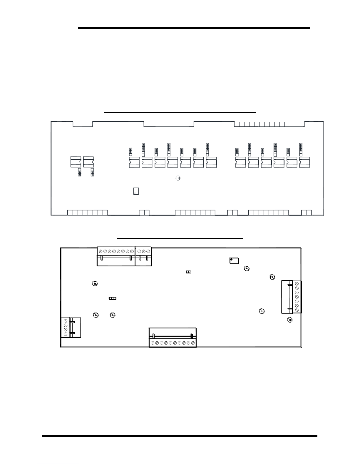
4.4. I/O, FEATURES, AND DISPLAYS
Full status monitoring is available through discrete I/O points located on the 3460M6
board. Most of the I/O can be configured for different modes of operation with jumpers.
This allows flexibility in the installation for remote control and monitoring of the system.
Figure 4-1: 3460M6 Status Interface Board Layout
K10
RMT PCC
RMT VF
NO
RMT OT
RMT RTR
NO
JP1
NC
LOC RTR
JP3
JP2
NC
NO
LOC OT
NC
NC
NO
JP4
LOC VF
NC
JP5
NO
NC
JP6
NO
LOC PCC
NC
JP7
NO
NC
JP8
NO
K1
K6
K2
K3
K4
K5
K7
K8
RMT IUV
RMT FLT
NC
JP10
NO
LOC IUV
NC
JP11
NO
LOC RTA
NC
JP12
NO
RMT RTA
NC
NO
JP13
JP14
NC
NO
K16
JP16
NC
NO
K12 K11
K13
K14
ENABLE
NC
RUN
K15
NO
JP15
TB7
2
3
4 1
10 789 6
5
432 1
TB6
7
141312 11
10 89 6
5
432 1
TB5
TB1
3
1 2
7 86
5
4 2 1
TB3
4321
86 7
5
TB4
1 432
7658
TB10
3460M6
2 1
TB8
2 1
TB9
LD1
R31
IUV
Figure 4-2: 3460C1 Control Board Layout
1
TB3
TB4
1
LD2
TB1
LD5
TB2
1
TEST
INT
J4
EXT
LD6
+15V
TB5
1
R7
THRESHOLD
LD3
RIDE-THRU
READY
-15V
LD7
LD4
COMPLETE
PRECHARGE
ACTIVE
RIDE-THRU
3460C1
CONTROL BOARD
by BONITRON
LD1
BLOWN FUSE
J1
T.O.
Page 25
User’s Manual
25
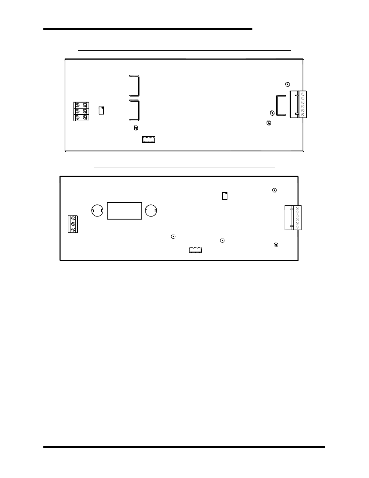
Figure 4-3: 3460D5 Power Supply Board Layout (for 380V and 460V)
3460D5 by BONITRON
31
TB1
LD1
TB2
1 3
BUS OK
TB3
1
LD4
LD3
+23V
-23V
LD2
ISO 23V
R3
Figure 4-4: 3460D6 Power Supply Board Layout (for 575V)
3460D6
31
TB1
LD4
TB2
1 3
BUS OK
TB3
1
LD2
LD1
+23V
-23V
LD3
ISO 23V
R30
RIDE-THRU DC TO DC SUPPLY BOARD
LOW BUS SENSE
ISO COM
ISO 24V
N/C
-24V
COM
+24V
L1
L2
C1
Bonitron, Inc
4.4.1. INPUT TERMINALS – 3460M6 TB7
The input terminals are located on TB7 of the 3460M6 board. They can use an
internal supply with a dry contact or an external 24VDC.
4.4.1.1. ENABLE INPUT - TB7-1, 2
The Enable input is used to allow the M3460 to operate. This signal can
be configured for either enable or disable operation.
This input operation is configured with jumper JP15.
The input operation is set to "Enable" with JP15 set to "NO", and the
M3460 will operate when 24VDC is applied to the input.
The input operation is set to "Disable" with JP15 set to "NC", and the
M3460 will be inhibited and not operate when 24VDC is applied to the
input.
Connect the 24V positive to TB7-1 and the 24V common to TB7-2.
JP16 is a spare enable input that is not currently used and should be left
in the same position as JP15 to avoid any confusion.
With the M3460R, the Overtemperature output status contact at TB5
should be used to disable the M3460R. This can be done by connecting
24V positive to TB5-3, connecting TB5-4 to TB7-1, and connecting the
24V common to TB7-2.
Page 26
M3460
26
With the M3460B, the Overtemperature and Input Undervoltage output
status contacts should be used to disable the M3460B. This can be done
by connecting 24V positive to TB5-3, connecting TB5-4 to TB5-13,
connecting TB5-14 to TB7-1, & connecting the 24V common to TB7-2.
The factory default setting is to have the operation set to "Enable".
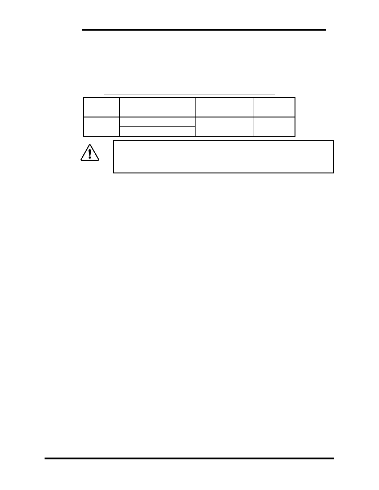
Table 4-1: 3460M6 Enable Input Logic Jumper Details
JUMPER
POSITION
FUNCTION
3460M6
FIELD TERMINALS
FACTORY
SETTING
JP15
NO
Enable
TB7 - 1, 2
NO (Enable)
NC
Disable
CAUTION!
THE M3460 MAY NOT OPERATE CORRECTLY IF THE UNIT IS NOT PROPERLY
CONFIGURED. PAY SPECIAL ATTENTION TO THIS CONFIGURATION, AS THIS
CAN CAUSE THE UNIT TO NOT PROTECT THE DRIVE IN THE CASE OF A POWER
SAG OR OUTAGE.
4.4.1.2. TEST INPUT - TB7 - 3, 4
The Test input is used to make the M3460 go into Test mode.
Connect 24V positive to TB7-3 and 24V common to TB7-4 to force the
M3460 into Test mode.
When the DP10 display is used, pressing the test button on the display
will put the M3460 into Test mode.
4.4.2. OUTPUT TERMINALS - 3460M6 TB5, TB6
The status of the M3460 can be monitored from two locations.
TB5 has individual isolated contacts for indication and TB6 has indicators that
have a single common on TB6-8. In general, TB6 is used to connect the DP10
or DD5 display panel, but is not restricted to that use.
All the status outputs can be configured with jumpers to be normally open (NO)
or normally closed (NC). In the descriptions below, the operation is described
for the jumpers to be set in the normally open position.
The outputs are not polarized.
4.4.2.1. RIDE-THRU READY - TB5 - 1, 2 & TB6 - 5
This output closes when the M3460 is ready to operate and has no faults.
This indicates the Enable input is active, the precharge is complete, and
all the stage fuses are intact. This can be used as a general status
indication.
The output configuration can be set to normally open or normally closed
with Jumper JP2 for TB5-1, 2 and with JP1 for TB6-5.
4.4.2.2. OVERTEMPERATURE - TB5 - 3, 4 & TB6 - 4
This output opens when the temperature of any heatsink in the M3460 is
above 160F. The contact will close again when the temperature goes
below 140F. This does not stop the M3460 from operating, and care
must be taken so that the M3460 is turned off before damage can occur
to the internal power stages.
The output configuration can be set to normally open or normally closed
with Jumper JP4 for TB5-3, 4 and with JP3 for TB6-4.
Page 27

User’s Manual
27
4.4.2.3. VOLTAGE FAULT - TB5 - 5, 6 & TB6 - 3
On M3460R models, this output opens when any phase from the input
AC line is missing.
On M3460B models, this output opens when the output DC Bus drops
below a preset threshold level. This is an indication the M3460B is not
holding the DC Bus up and an Undervoltage Fault on the attached drive
is possible. The default setting for this output is approximately 35V below
the threshold level. This level can be adjusted in the field as described in
Section 4.7.
The output configuration can be set to normally open or normally closed
with Jumper JP6 for TB5-5, 6 and with JP5 for TB6-3.
4.4.2.4. GENERAL FAULT - TB5 - 7, 8
This output is a combination of the Voltage Fault, Overtemperature, and
Ride-Thru Ready status contacts. It will open if any of these faults open,
after a 3 second delay.
The output configuration can be set to normally open or normally closed
with Jumper JP10 for TB5-7, 8. This output is not on TB6.
4.4.2.5. PRECHARGE COMPLETE - TB5 - 9, 10 & TB6 - 2
This output will close when the M3460 has been enabled and gone
through the precharge cycle.
The output configuration can be set to normally open or normally closed
with Jumper JP8 for TB5-9, 10 and with JP7 for TB6-2.
4.4.2.6. RIDE-THRU ACTIVE - TB5 - 11, 12 & TB6 - 6
This output will close when the M3460 is regulating the output DC bus of
the system. This indicates that the power input on the connected
equipment has sagged or failed. This output will also close when the unit
is put into Test mode with the Test input, assuming the attached drive is
loaded.
This output will latch on for 3 seconds after activity has stopped. The 3
second pulse allows a monitoring system to ensure capture of the event,
or to indicate when the M3460 is being forced into operation when the
power feed may be normal.
The output configuration can be set to normally open or normally closed
with Jumper JP14 for TB5-11, 12 and with JP13 for TB6-6.
4.4.2.7. INPUT UNDERVOLTAGE - TB5 - 13, 14 & TB6 - 7
This output indicates that the input voltage to the M3460 has dropped
below a preset threshold. This is generally used when a storage device
must be protected from over discharge. The default level for this output
is dependent on the nominal system voltage, and is listed in Tables 6-3
and 6-4.
This level can be adjusted in the field as described in Section 4.6.
Page 28
M3460
28
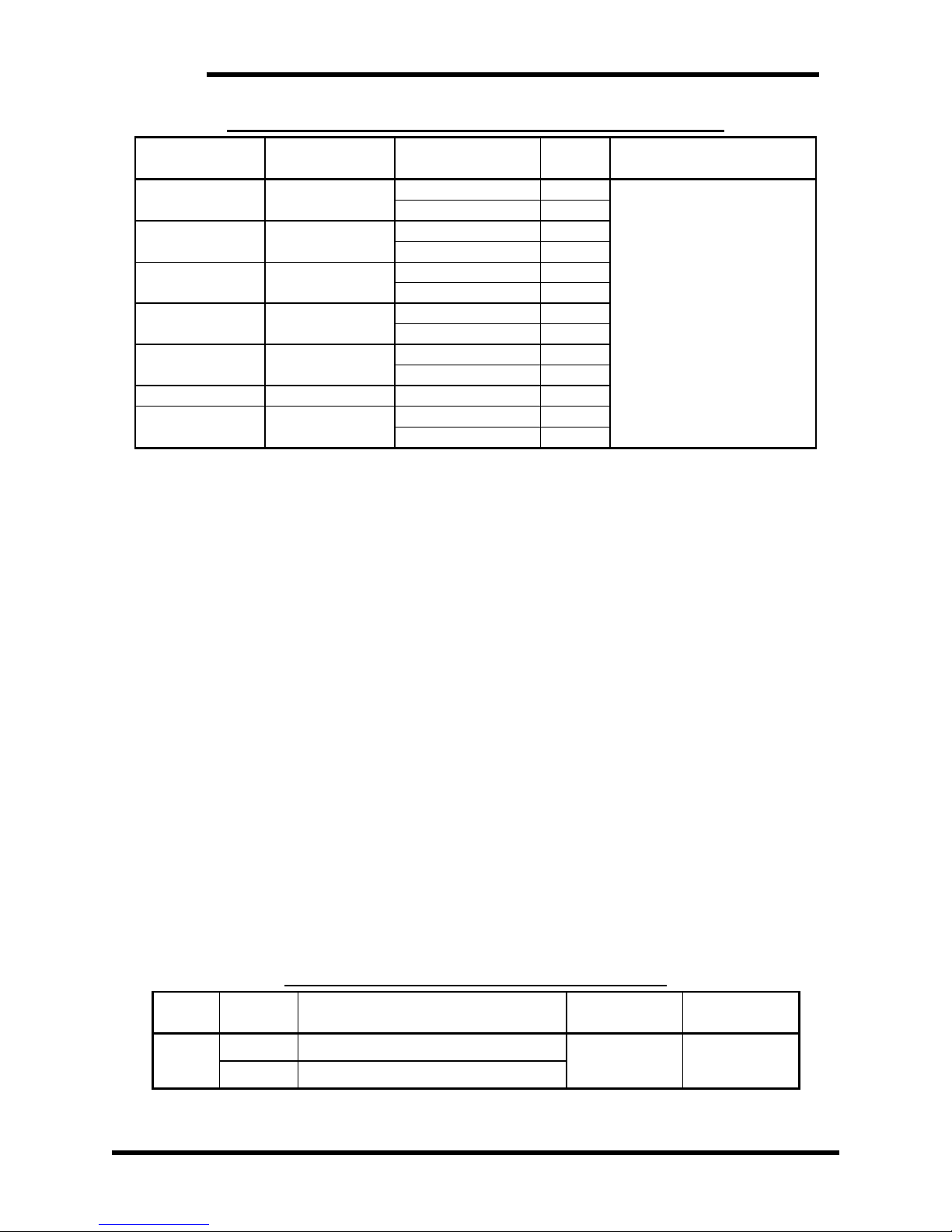
Table 4-2: 3460M6 Status Output Signal Logic Jumper Details
OUTPUT
ABBREVIATION
3460M6
FIELD TERMINALS
JUMPER
FACTORY SETTING
Voltage
Fault
VF
TB6 – 3
JP5
Normally Open (N.O.)
TB5 – 5, 6
JP6
Over
Temperature
OT
TB6 – 4
JP3
TB5 – 3, 4
JP4
Precharge
Complete
PCC
TB6 – 2
JP7
TB5 – 9, 10
JP8
Ride-Thru
Active
RTA
TB6 – 6
JP13
TB5 – 11, 12
JP14
Ride-Thru
Ready
RTR
TB6 – 5
JP1
TB5 – 1, 2
JP2
General Fault
FLT
TB5 – 7, 8
JP10
Input
Undervoltage
IUV
TB6 – 7
JP11
TB5 – 13, 14
JP12
4.4.3. LOCAL I/O POWER SUPPLY - TB6 - 1, 9
The I/O contacts for the M3460 can be supplied by the internal supply available
on TB6 – 1, 9. TB6 – 1 is 24VDC+ and the common is on TB6 – 9.
It is not recommended to use an external power supply connected in parallel
to the internal supply. If an external supply is used, terminals TB6 – 1 and TB6
– 9 should not be used.
When the DP10 analog display is installed with the M3460, this internal power
supply is used to drive the I/O on the display panel.
4.4.4. RUN TIMEOUT SELECTION
The ride-thru operation can be timed out automatically during a power quality
event or testing. This allows internal monitoring of operation to prevent
overheating of the unit. Jumper J1 on the 3460C1 control board can be used
to limit the operation time to 2 seconds.
If jumper J1 is OFF the M3460 will operate for 2 seconds and then stop
operating. Once the power quality event ends or Test input is removed the
M3460 can operate again after a 4 second delay.
If jumper J1 is ON the M3460 will operate as long as the DC bus is below the
DC Bus Threshold voltage during a power quality event, or as long as the
"Test" input is active.
The default setting for M3460R is placing J1 in the “OFF” position.
The default setting for M3460B is placing J1 in the “ON” position.
Table 4-3: Run Timeout Jumper Configurations
JUMPER
POSITION
FUNCTION
M3460R
SETTING
M3460B
SETTING
J1
ON
No Run Timeout
OFF
ON
OFF
Run Timeout set to 2 seconds
Page 29
User’s Manual
29
DANGER!
IF J1 IS LEFT ON, THE M3460 WILL RUN CONTINUOUSLY AND CAN OVERHEAT.
DAMAGE CAN OCCUR IF THE UNIT IS OPERATED BEYOND ITS RATINGS FOR DURATION
OR TEMPERATURE.
4.4.5. TEST TIMER SELECTION
The Test operation can be selected to be “real time” or a pre-determined, two
second pulse.
Jumper J4 located on the 3460C1 control board is used for this selection.
If J4 is in the “INT” position, the DC Bus will rise for 2 seconds every time the
Test input is active.
If J4 is in the “EXT” position, the DC Bus will rise for as long as the Test input
is active, unless J1 is selected to time out after 2 seconds.
The default setting is the “EXT” position.
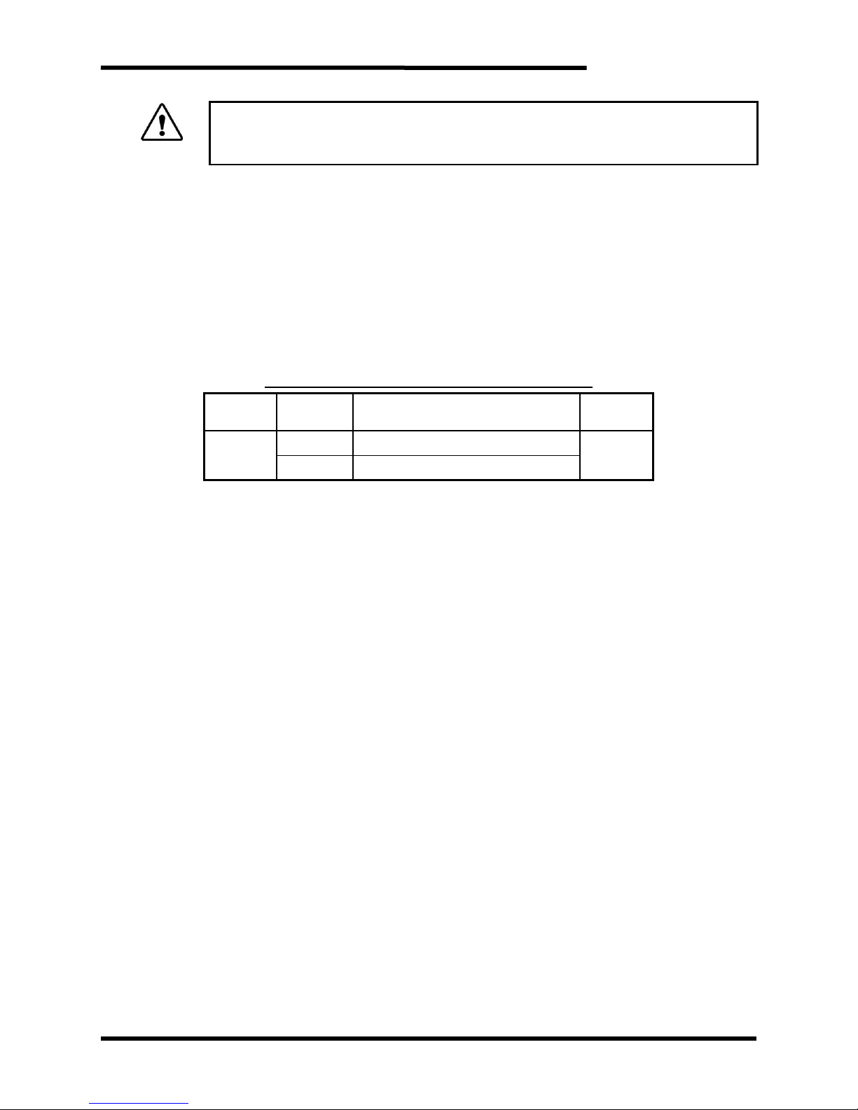
Table 4-4: Test Timer Jumper Configurations
JUMPER
POSITION
FUNCTION
FACTORY
SETTING
J4
INT
Sets test timer to 2 seconds
EXT
EXT
Test timer is real time
4.4.6. INDICATORS
There are several light-emitting diodes (LEDs) used to indicate the status of
the M3460. These are found on the 3460C1, 3460M6, 3460D5 and 3460D6
boards. See Figures 4-1, 4-2, & 4-3, 4-4.
4.4.6.1. POWER – 3460C1 - LD6, LD7
The +15V and -15V lights will illuminate when the internal power supply
is operating properly.
4.4.6.2. RIDE-THRU READY (RTR) – 3460C1 - LD3
The Ride-Thru Ready light will illuminate when the M3460 has been
enabled and there are no faults. This can be used as a general status
indication.
4.4.6.3. PRECHARGE COMPLETE (PCC) – 3460C1 - LD4
The Precharge Complete light will illuminate when the M3460 internal bus
capacitors have been precharged.
4.4.6.4. BLOWN FUSE (BF) – 3460C1 - LD5
The Blown Fuse light will illuminate when an internal IGBT stage fuse has
blown.
4.4.6.5. RIDE-THRU ACTIVE (RTA) – 3460C1 - LD2
The Ride-Thru Active light will illuminate while the M3460 is regulating
the DC bus or when the M3460 is put into Test mode. If the M3460 is
unloaded or lightly loaded, this light may not illuminate.
4.4.6.6. TEST – 3460C1 - LD1
The Test light will illuminate when the M3460 is put into Test mode. If the
M3460 is unloaded or lightly loaded, this light may not illuminate.
Page 30
M3460
30
4.4.6.7. NO FAULT (NFLT) – 3460M6 - LD1
The No Fault light will illuminate during normal operation. It will go out
with a Ride-Thru Ready, Overtemperature, or Voltage Fault, after a three
second delay.
4.4.6.8. OUTPUT UNDERVOLTAGE (OUV) –3460D5 – LD1, 3460D6-LD4
The Output Undervoltage fault will happen if the DC bus is approximately
35V below the threshold setting. If the DC bus drops 35V below the
threshold setting, the light will go out. This is an indication the M3460 is
not regulating the DC bus and an undervoltage fault on the attached
equipment is possible. This light is also indicated as “BUS OK”.
4.4.7. FAN TIMER
The M3460B is equipped with fans to keep the heatsinks cool while the unit is
active. These fans are controlled by a timer relay on the front of the unit. This
timer relay is set at the factory to run for approximately 2 hours after the
M3460B module becomes active. This setting should not be adjusted as it may
affect the ability of the M3460B module to operate properly for its time
specification.
4.4.8. DISPLAY OPTIONS
There are two display options available for local indication. They are designed
to be mounted to the door or deadfront of a drive cabinet or system. The
displays show the M3460 operating status and also permit a system test to be
performed. The DD5 digital display system has many more features than the
DP10 analog display, including outage and fault logging. Please refer to the
KIT 3660DD5 manual for a full description of the features.
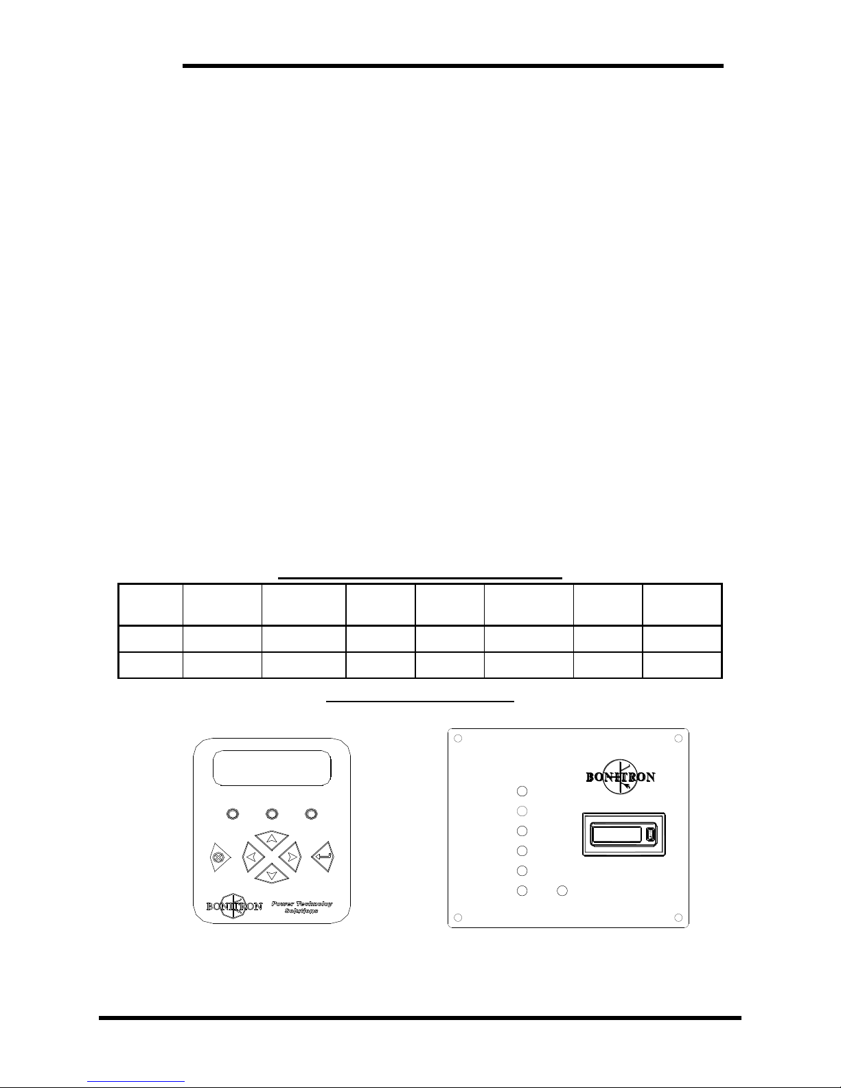
Table 4-5: Display Panel Configurations
DISPLAY
MODEL
LOCAL
INDICATORS
VOLTMETER
AMMETER
TOTAL
COUNTER
RESETTABLE
COUNTER
ACTIVITY
LOGGING
LOCAL TEST
INITIATION
DD5
✓ ✓ ✓ ✓ ✓ ✓ ✓
DP10 ✓ ✓
✓
Figure 4-5: Display Panels
DD5
DP10
ACTIVE
ACTIVE CYCLES
VOLTAGE
TEMP
FAULT
OVER
SYSTEM
TEST
COMPLETE
PRECHARGE
RIDETHRU
RIDETHRU
READY
POWER
Page 31
User’s Manual
31
4.4.8.1. DD5 DIGITAL DISPLAY
The KIT 3660DD5 digital display has many features and control modes
that can be used to monitor, test and log information about the M3460
and its activity.
Below are basic operation instructions. Please refer to the KIT 3660DD5
manual for detailed instructions and configuration information.
The KIT 3660DD5 power supply should not be connected to earth
ground.
The digital display can also be used to monitor charging and storage
modules for Ride-Thru systems.
DIGITAL DISPLAY INPUTS
There are two remote inputs to control the activity of the M3460, Enable
and Test. They allow remote initiation of these inputs, but the digital
display system allows the M3460 to be tested locally.
DIGITAL DISPLAY OUTPUTS
There are two outputs that can be configured for various indications on
the digital display.
DEFAULT OPERATION
When the M3460 is ordered with the KIT 3660DD5 digital display, the
factory settings are for Automatic Control mode.
The M3460R will be disabled locally under the following conditions:
• Overtemperature
• Runtime Exceeded
The M3460B will be disabled locally under the following conditions:
• Input Undervoltage
• Overtemperature
• Runtime Exceeded
The default operation allows for the most complete protection for the
M3460 but these can be reconfigured if required.
CAUTION!
DISABLING THESE FAULTS CAN DAMAGE THE M3460 BY FORCING
IT TO OPERATE OUTSIDE OF DESIGN PARAMETERS!
4.4.8.2. DP10 ANALOG DISPLAY
The DP10 has LED indicators for the following status outputs:
• Power
• Precharge Complete
• Ride-Thru Ready
• Ride-Thru Active
• Voltage Fault
• Overtemperature
In addition, there is a total cycle counter that can be reset. It indicates the
number of times the M3460 has been active since the last reset. This
number will increase when there is a power quality event, or when the
system is tested.
There is also a local test button that can be used to initiate a system test.
Page 32
M3460
32
4.5. DC BUS THRESHOLD VOLTAGE SETTING
The DC bus threshold voltage is the voltage at which the M3460 maintains the DC bus
during a power quality event. Whenever the output DC bus voltage drops below the
DC bus threshold voltage setting, the M3460 becomes active to regulate the DC bus
to the setpoint voltage.
The DC bus threshold voltage is important to the installation in that if it is set too low,
the attached drive may trip on an undervoltage fault. If it is set too high, then minor
power disturbances, such as line notching or high harmonics that would not normally
cause the drive to have problems may cause the M3460 to become active when there
is no need. If this is a constant or frequent occurrence, the M3460 may overheat and
not be available in the event of an actual sag or outage.
The M3460 DC bus threshold voltage setting is determined by the drive installation.
Consult the manufacturers' specifications on the attached drive, and make sure that
the DC bus threshold voltage is above this value. For instance, many 460-480VAC
input drives have an undervoltage trip point of 400VDC. This may allow the drive to
keep operating, but the DC bus voltage may not be enough to allow the drive to operate
at full power. Therefore, it's useful to set the DC bus threshold voltage setting above
this value.
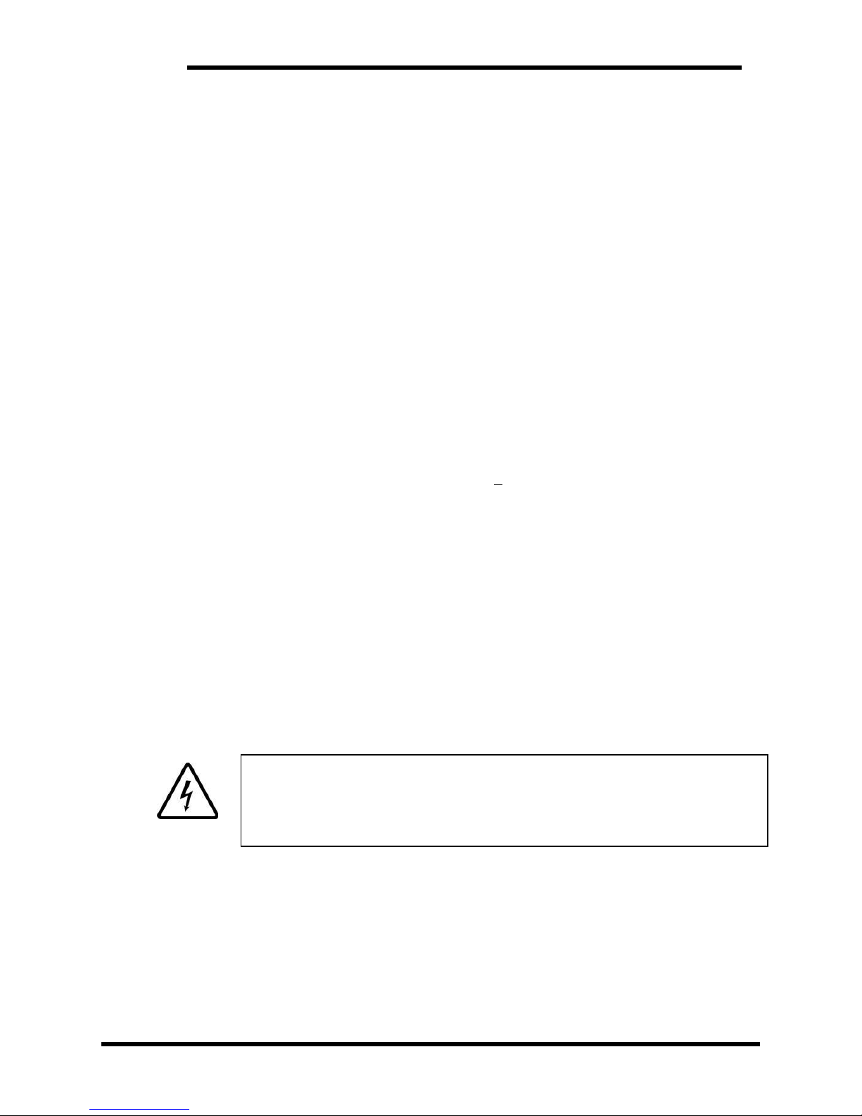
Generally, the DC bus threshold voltage should be set at 10% below the nominal DC
bus level. Use the following formula to calculate this value:
An actual on-site check may be performed to determine the loaded DC bus level as
well as the amount of ripple present on the DC bus.
If you find that your incoming AC power is susceptible to long term sags or conditions
below 10%, the M3460 may become active when not needed. In this case, the DC bus
threshold voltage setting should be lowered to allow the M3460 to only be active during
a true power quality event. The M3460 should not become active during normal
operation.
The DC bus threshold voltage is factory preset on all M3460 modules according to
Table 6-2 of this manual. However, field adjustment of this setting may be required to
achieve the optimum setpoint level for any given system. There are two ways to
determine the DC bus threshold voltage described below. Be sure to read through both
methods completely before attempting any adjustment of the DC bus threshold voltage
setting.
DANGER!
• HI GH V OL T AG ES W I TH R E SP EC T T O CHA SS IS AR E P RE SE N T!
• NE VE R US E A N UN I NS U LA TE D T OO L OF AN Y KI ND!
• F AILURE TO HEED THESE WARNINGS MAY RESULT
IN SERIOUS INJURY OR DEATH!
4.5.1. DETERMINING THE DC BUS THRESHOLD VOLTAGE SETTING
DIRECTLY (M3460R MODELS)
Checking the DC bus threshold voltage setting directly requires the AC power
to be removed from the M3460R. If the M3460R DC bus is not connected to
the output of the drive, this can be done without powering down the drive.
Otherwise, the drive must have the AC power removed from it as well. It may
be difficult to get an accurate reading using a digital voltmeter due to the time
Page 33

User’s Manual
33
it takes to calculate and average the reading. Use an analog meter if possible.
1. Monitor the output DC bus of the M3460R, or the input DC bus to the
drive, if connected.
2. Remove input voltage supply from system.
3. As the DC bus voltage drops to the DC bus threshold voltage setting,
the M3460R will become active and maintain the DC bus voltage at the
threshold voltage setpoint for approximately 1 second while the
M3460R input filter capacitor discharges. The DC bus will then continue
to drop.
4. Read the DC bus voltage as it is being maintained. This is the DC bus
threshold voltage setting.
4.5.2. DETERMINING THE DC BUS THRESHOLD VOLTAGE SETTING
DIRECTLY (M3460B MODELS)
Checking the DC bus threshold voltage setting directly requires disconnecting
the M3460B DC bus from the drive DC bus while the battery bank supplies
power to the M3460B.
1. Monitor the output DC bus of the M3460B.
2. Disconnect the M3460B DC bus from the drive DC bus.
3. The M3460B should now be active and the voltage at the M3460B
output DC bus is the threshold setting.
4.5.3. DETERMINING THE DC BUS THRESHOLD VOLTAGE SETTING
USING THE TEST MODE
The DC bus threshold voltage setting may be checked with the drive connected
using the test input to put the M3460 in Test mode. This raises the DC bus
voltage approximately 50-100V above the actual DC bus threshold voltage
setting, and is a fair indication of how the system is set. This has the advantage
of not having to remove the AC power, and can actually be done while the
system is loaded.
Please note:
• If heavily loaded, the M3460 may run in current limit and the DC bus voltage
may not rise as much as if it were unloaded.
• If the DC bus threshold voltage is set too high, the DC bus test voltage may
be limited by the overvoltage setting of the M3460, thus providing an
inaccurate result.
The M3460 may shutdown from the timeout feature, depending on the load.
1. Monitor the output DC bus of the M3460, or the input DC bus to the
drive, if connected.
2. Enable the Test input, or initiate a test with the display.
3. Monitor the DC bus voltage while the M3460 is in Test mode. This is
the DC bus test voltage setting.
The DC bus test voltage setting is approximately 50-100V higher than the DC
bus threshold voltage setting.
For example, for an M3460 with an input voltage of 460VAC, the DC bus
threshold voltage setting is preset to be 585VDC and the DC bus test voltage
setting is preset for an increase of 100VDC. Initiating the test described above
would cause the DC bus voltage to rise to 685VDC (585VDC + 100VDC).
Subtracting the DC bus test voltage (100VDC) from this reading shows that the
Page 34

M3460
34
actual DC bus threshold voltage setting is 585VDC.
4.5.4. ADJUSTING THE DC BUS THRESHOLD VOLTAGE SETTING
Adjustment of R7 on the 3460C1 control board (see Figure 4-2) is used to
adjust the DC bus threshold voltage setting. Adjusting the pot in a clockwise
direction will raise the setting. Alternately, a counter-clockwise adjustment of
the pot will lower the setting.
After making the adjustments, repeat the test to verify the new setpoint. Fine
tune the adjustment and retest as necessary.
4.6. INPUT UNDERVOLTAGE (IUV) LEVEL ADJUSTMENT
This output indicates that the input voltage to the M3460 has dropped below a preset
threshold. This is generally used when a storage device must be protected from over
discharge. The default level for this output is dependent on the nominal system
voltage, and is listed in Table 6-3 and Table 6-4.
Adjustment of pot R31 on the 3460M6 interface board (see Figure 4-1) is used to set
the input undervoltage level. Adjusting the pot in a clockwise direction will raise the
setpoint level and a counter-clockwise adjustment of the pot will lower the setpoint
level.
4.7. OUTPUT UNDERVOLTAGE LEVEL ADJUSTMENT
This output indicates that the output voltage to the Drive DC Bus has dropped below
a preset threshold. This generally means the M3460 is not maintaining the DC Bus
and an Undervoltage fault is possible on the attached Drive. The default level for this
output is approximately 35V below the threshold level.
Adjustment of pot R3 on the 3460D5 board or pot R30 on 3460D6 board is used to set
the "Low DC Bus" voltage level. Adjusting the pot in a clockwise direction will raise the
setpoint level and a counter-clockwise adjustment of the pot will lower the setpoint
level (see Figure 4-3, 4-4).
Page 35

User’s Manual
35
5. START-UP, MAINTENANCE AND TROUBLESHOOTING
5.1. M3460R START-UP / FIELD TEST PROCEDURE
1. Ensure the M3460R has been properly installed and is disabled.
2. Ensure the M3460R DC bus is disconnected from the drive DC bus.
3. Ensure the drive is operating properly with the M3460R disconnected.
4. Apply power to the input of the M3460R and observe the following
conditions:
• DC bus voltage should rise
• +15V light on 3460C1 board should be ON
• -15V light on 3460C1 board should be ON
• Precharge Complete light on 3460C1 board should be OFF
• Ride-Thru Ready light on 3460C1 board should be OFF
• Ride-Thru Active light on 3460C1 board should be OFF
• Blown Fuse light on 3460C1 board should be OFF
• Test light on 3460C1 board should be OFF
• No Fault light on 3460M6 board should be OFF
• Bus OK light on 3460D5 / 3460D6 board should be ON
• All status outputs are in the expected state. If there are faults on the system,
check the configuration of the status output jumpers.
5. Enable the M3460R with either the enable input or the digital display.
• Ride-Thru Ready and Precharge Complete lights on 3460C1 board should
turn ON
• No Fault light on 3460M6 board should turn ON
6. Initiate the test mode with the Test input or display panel.
• The DC bus should rise for as long as the test is performed. A timeout may
occur, depending on the state of J1 and J4 on the 3460C1 board and the
load on the M3460R.
7. Turn off the power to the M3460R and watch the DC bus voltage fall.
• The Ride-Thru Active light should turn ON when the M3460R starts to
operate.
• The DC bus will hold at the DC bus threshold voltage setting momentarily
while the filter capacitors drain.
8. With the M3460R and drive power off, connect the DC bus of the M3460R
to the DC bus of the drive.
9. Turn on power to the drive and ensure it is working properly without any
fault, the drive must be ON before applying power to the Ride-Thru.
apply power to M3460R and ensure proper function without any faults.
10. Monitor the DC bus voltage and current with the display or with separate
meters. Also, monitor the AC input current to the attached drive.
11. Load the drive as much as practical and put the M3460R into Test mode
by activating the Test input or using the display panel.
• DC bus voltage should rise to the test boost level.
• Motor should not lose speed or torque.
• DC bus current should flow from M3460R to drive.
• Drive input current should decrease.
The M3460R and drive system should now be ready to be put into service.
Page 36

M3460
36
CAUTION!
• IF THE M3460R IS ACTIVE FOR LONGER THAN THE TIMEOUT SETTING, IT WILL
SHUT DOWN SWITCHING AND THE DC BUS WILL DROP TO THE NORMAL LEVEL.
• IF THE OUTPUT DC BUS DROPS BELOW 70% THE M3460R WILL HAVE TO GO
THROUGH PRE-CHARGE AGAIN.
5.2. M3460B START-UP / FIELD TEST PROCEDURE
1. Ensure the M3460B has been properly installed and is disabled.
2. Ensure the M3460B DC bus is disconnected from the drive DC bus.
3. Ensure the drive is operating properly with the M3460B disconnected.
4. Apply battery bank power to the input of the M3460B and observe the following
conditions:
DC bus voltage should rise to approximately the battery bank voltage
+15V light on 3460C1 board should be ON
-15V light on 3460C1 board should be ON
Precharge Complete light on 3460C1 board should be OFF
Ride-Thru Ready light on 3460C1 board should be OFF
Ride-Thru Active light on 3460C1 board should be OFF
Blown Fuse light on 3460C1 board should be OFF
Test light on 3460C1 board should be OFF
No Fault light on 3460M6 board should be OFF
Bus OK light on 3460D5 /3460D6 board should be OFF
All status outputs are in the expected state. If there are faults on the system,
check the configuration of the status output jumpers.
5. Enable the M3460B with either the enable input or the digital display.
• Ride-Thru Ready and Precharge Complete lights on 3460C1 board should
turn ON
• No Fault light on 3460M6 board should turn ON
• Bus OK light on 3460D5 /3460D6 board should turn ON
• Ride-Thru Active light should turn ON and M3460B should start to operate
• The DC bus will hold at the DC bus threshold voltage setting
6. Initiate the test mode with the Test input or display panel.
The DC bus should rise for as long as the test is performed. A timeout may
occur, depending on the state of J1 and J4 on the 3460C1 board and the
load on the M3460B.
7. Turn off the battery bank power to the M3460B and connect the DC bus of the
M3460B to the DC bus of the drive.
8. Turn on the AC power to the drive, then battery bank power to the M3460B
the drive must be ON before applying power to the Ride-Thru.
9. Monitor the DC bus voltage and current with the display or with separate
meters. Also, monitor the AC input current to the attached drive.
10. Load the drive as much as practical and put the M3460B into Test mode by
activating the Test input or using the display panel.
DC bus voltage should rise to the test boost level.
Motor should not lose speed or torque.
DC bus current should flow from M3460B to drive.
Drive input current should decrease.
The M3460B and drive system should now be ready to be put into service.
Page 37
User’s Manual
37
CAUTION!
• IF THE M3460B IS ACTIVE FOR LONGER THAN THE TIMEOUT SETTING, IT WILL SHUT
DOWN SWITCHING AND THE DC BUS WILL DROP TO THE NORMAL LEVEL.
• IF THE OUTPUT DC BUS DROPS BELOW 70% THE M3460B WILL HAVE TO GO
THROUGH PRE-CHARGE AGAIN.
5.3. MAINTENANCE ITEMS
The M3460 is designed to require very little maintenance. Bonitron recommends a
yearly test of the system in order to ensure the system is functioning properly. If the
system is equipped with displays, then the cycle counters should indicate the number
of events since the last reset. If there are more than 10 events per month, the DC bus
threshold voltage setting should be checked and/or adjusted.
5.3.1. CAPACITOR REPLACEMENT RECOMMENDATIONS
The M3460 uses high quality aluminum electrolytic capacitors and is designed
for long life without maintenance. While a typical inverter may require capacitor
replacement after a certain time due to the heavy ripple currents, the M3460
typically is in a standby mode waiting for a power disturbance, and by design
has 50% more capacitance than needed.
The capacitors are rated for 11 years MTBF if ambient temp is 50°C, capacitors
are held at 100% rated voltage, and caps run full ripple current at 1% duty.
With typical operating conditions of 35°C, caps running at 75% rated voltage,
and a duty cycle of one event per month, Bonitron recommends the capacitors
be checked or replaced every 20 years.
The recommended test is to measure the voltage across each series set of
capacitors. Any voltage difference greater than 15% between each set of
series caps would indicate a change in value in one cap and would constitute
a more detailed out of circuit capacitance check. (A difference of 5% is allowed
at time of production.)
Testing the capacitors in the unit requires trained personnel, and should only
be attempted observing appropriate safety and arc-flash precautions when
working on live high voltage equipment.
DANGER!
• HIGH VOLTAGES ARE PRESENT!
• NEVER ATTEMPT TO OPERATE THIS PRODUCT WITH THE ENCLOSURE COVER
REMOVED!
• NEVER ATTEMPT TO SERVICE THIS PRODUCT WITHOUT FIRST DISCONNECTING
POWER TO AND FROM THE UNIT.
• ALWAYS ALLOW ADEQUATE TIME FOR RESIDUAL VOLTAGES TO DRAIN BEFORE
OPENING THE ENCLOSURE.
• FAILURE TO HEED THESE WARNINGS MAY RESULT IN SERIOUS
INJURY OR DEATH!
Page 38

M3460
38
5.3.2. CAPACITOR TESTING PROCEDURE
1. Open the panel door to expose the capacitor bank.
1. Measure voltage across each cap and make note for future reference.
2. Any voltage difference more than 15% indicates a substantial change in
capacitance.
Example: DC bus = 540V, each series cap = 270V
15% of 270 = 40.5V
cap 1 = 290V
cap 2 = 250V
Turn off power, discharge the capacitor bank voltage and replace both
capacitors if the difference is more than 15%.
5.3.3. CLEANING
It may be necessary to clean off dust, debris, or chemical build-up on high
voltage bus bars or other exposed components. If cleaning is needed:
• Remove power and allow all voltages to drain.
• Check for residual voltages with meter.
• Clean affected areas with rag, brush or denatured alcohol, depending on
the type of contamination.
• Once area is clean and dry, reapply power.
5.3.4. FANS
Bonitron estimates fan life to be longer than 20 years in a properly adjusted
M3460B in a clean cool environment, 4 years under constant running
conditions with high ambient temperatures.
5.3.5. HEATSINKS
Dirt can build up on heatsink surfaces degrading its ability to dissipate heat.
The heatsinks should be checked for large amounts of deposits and cleaned
as needed. The maintenance interval depends upon the amount of activity and
the environment inside the cabinet.
Checking the heatsink should be included when checking for fan operation.
Page 39

User’s Manual
39
5.4. TROUBLESHOOTING
Below are suggestions on how to check some common issues.
If you continue to have problems after going over this list, please contact Bonitron.
Table 5-1: Troubleshooting Guide
SYMPTOM
ACTION
No lights are ON
▪ Check incoming power.
Ride-Thru will not
become active
▪ Check Enable Input. See Section 4.4.1.1
▪ Check input and output fuses.
Test Mode Does Not
Raise Output Voltage
▪ Check Enable Input. See Section 4.4.1.1
▪ Check Test Input. See Section 4.4.1.2
▪ Check input and output fuses.
▪ Check threshold voltage setting. See Section 4.5.4.
Stays in Test Mode
▪ Check Test Input. See Section 4.4.1.2
Ride-Thru Ready light is
OFF or Ride-Thru Ready
output is open
▪ Check Enable Input. See Section 4.4.1.1
▪ Check IGBT fuses.
▪ Check 3460M6 jumpers. See Table 4-2
Precharge Complete
light is OFF or
Precharge Complete
output is open
▪ Check Enable Input. See Section 4.4.1.2
▪ Check 3460M6 jumpers. See Table 4-2
▪ Check Drive Bus voltage level.
Voltage Fault output is
open
▪ Check input fuses (for M3460R models)
▪ Check Drive Bus level and see Section 4.7 (for M3460B models)
▪ Check jumpers on 3460M6 board. See Table 4-2
Overtemperature output
is open
▪ Check jumpers on 3460M6 board. See Table 4-2
▪ Check threshold voltage setting. See Section 0
General Fault output is
open
▪ Check Ride-Thru Ready output
▪ Check Voltage Fault output
▪ Check Overtemperature output
▪ Check jumpers on 3460M6 board. See Table 4-2
Ride-Thru Active output
is closed when Ride-
Thru is not active
▪ Check Drive Bus voltage.
▪ Check threshold voltage setting. See Section 4.5.4
▪ Check jumpers on 3460M6 board. See Table 4-2
Page 40
M3460
40
SYMPTOM
ACTION
Ride-Thru Active output
does not close or
Attached Drive Trips
during power quality
events
▪ Check Enable Input. See Sec. 4.4.1.1
▪ Check Ride-Thru Ready output.
▪ Check Precharge Complete output.
▪ Check IGBT fuses.
▪ Verify Ride-Thru is connected to the attached drive.
▪ Initiate Test Mode to ensure Ride-Thru is operating properly.
Input Undervoltage
output is open
▪ Check the DC input voltage. See Section 4.6
▪ Check jumpers on the 3460M6 board. See Table 4-2
Blown Fuse light is ON
▪ Check IGBT fuses.
DD5 display shows AC
voltages 2x greater than
what is correct or DC
voltages and DC
currents are zero
▪ Check the polarity of the 15V wires going to the current sensors. See
KIT 3660DD5 manual, Table 3-1 and Section 4.5.1.6.
CAUTION!
REPAIRS OR MODIFICATIONS TO THIS EQUIPMENT ARE TO BE PERFORMED
BY BONITRON APPROVED PERSONNEL ONLY. ANY REPAIR OR MODIFICATION
TO THIS EQUIPMENT BY PERSONNEL NOT APPROVED BY BONITRON WILL
VOID ANY WARRANTY REMAINING.
5.5. TECHNICAL HELP – BEFORE YOU CALL
If possible, please have the following information when calling for technical help:
• Exact model number of affected units
• Serial number of unit
• Name and model number of attached drives
• Name of original equipment supplier
• Brief description of the application
• The AC line to line voltage on all 3 phases
• The DC bus voltage
• KVA rating of power source
• Source configuration Wye/Delta and grounding
This information will help us support you much more quickly. Please contact us at
(615) 244-2825 or through www.bonitron.com
Page 41
User’s Manual
41
6. ENGINEERING DATA
6.1. RATINGS
Table 6-1: M3460 kW Ratings
DC BUS
CURRENT
(AMPS)
230VAC
SYSTEM
VOLTAGE
380-415VAC
SYSTEM
VOLTAGE
460VAC
SYSTEM
VOLTAGE
575VAC
SYSTEM
VOLTAGE
85 A
25 kW
43 kW
50 kW
60 kW
127 A
38 kW
65 kW
75 kW
90kW
170 A
50 kW
87 kW
100 kW
125 kW
255 A
75 kW
130 kW
150 kW
185 kW
340 A
100 kW
175 kW
200 kW
245 kW
425 A
125 kW
215 kW
250 kW
305 kW
425A only available with M3460R models
M3460B 15-minute kW rating is half that listed in Table 6-1
Table 6-2: Factory Setpoints for DC Bus Threshold and Test Boost Voltages
SYSTEM VOLTAGE
DC BUS THRESHOLD
TEST BOOST
230 VAC
285 VDC
+50 VDC
380 – 415 VAC
485 VDC
+100 VDC
460 VAC
585 VDC
+100 VDC
575 VAC
720 VDC
+120 VDC
Table 6-3: M3460R Minimum Input Voltages
SYSTEM
VOLTAGE
MINIMUM AC
INPUT VOLTAGE
MINIMUM DC INPUT
VOLTAGE (IUV LEVEL)
MINIMUM DC INPUT
REQUIRED FOR
PRECHARGE
COMPLETE (PCC)
230 VAC
115 VAC
160 VDC
270 VDC
380 – 415 VAC
190 VAC
265 VDC
445-487 VDC
460 VAC
230 VAC
320 VDC
540 VDC
575 VAC
287 VAC
400 VDC
675 VDC
Minimum AC input power required after PCC for full power operation with energy storage.
Minimum DC input required after PCC for full power operation with energy storage.
Table 6-4: M3460B Battery Bank Typical Values
SYSTEM
VOLTAGE
MINIMUM
BATTERY VOLTAGE
(IUV LEVEL)
NOMINAL
BATTERY
VOLTAGE
FULL /
FLOAT
BATTERY
VOLTAGE
EQUALIZE
BATTERY
VOLTAGE
230 VAC
200 VDC
240 VDC
270 VDC
277 VDC
380 – 415 VAC
340 VDC
408 VDC
459 VDC
470 VDC
460 VAC
400 VDC
480 VDC
540 VDC
554 VDC
575 VAC
500 VDC
600 VDC
675 VDC
692 VDC
Page 42
M3460
42
Table 6-5: M3460R Model Specifications for 230 – 480 VAC Systems
DC BUS
CURRENT
BACKPLATE
SIZE
CIRCUIT
CONFIGURATION
RECOMMENDED
FUSE RATING
SCCR
RATINGS
DRIVE BUS
AC LINE
85 A
R10
2-stage
80 A, 700 V
125 A, 600 V
10 kA
127 A
R10
2-stage
125 A, 700 V
200 A, 600 V
170 A
R9
4-stage
175 A, 700 V
250 A, 600 V
255 A
R11
4-stage
250 A, 700 V
400 A, 600 V
340 A
R11
4-stage
350 A, 700 V
500 A, 600 V
18 kA
425 A
R11
4-stage
400 A, 700 V
600 A, 600 V
The input power source must be capable of handling a 2-second current surge at twice the nominal rating
for the M3460R. Maximum duty cycle is 1% at full rated load.
Fuses recommended for use with the M3460R are Gould-Shawmut A70QS series, Buss FWP series, or
equivalent semiconductor fuses. These are required for UL 508C compliance.
Suitable for use on a circuit capable of delivering not more than 10,000 RMS symmetrical amperes, 700
volts maximum when protected by recommended fuses.
Suitable for use on a circuit capable of delivering not more than 18,000 RMS symmetrical amperes, 700
volts maximum when protected by recommended fuses.
Table 6-6: M3460B Model Specifications for 230 – 480 VAC Systems
DC BUS
CURRENT
BACKPLATE
SIZE
CIRCUIT
CONFIGURATION
RECOMMENDED
FUSE RATING
SCCR
RATINGS
DRIVE BUS
STORAGE BUS
85 A
R10
1-stage
80 A, 700 V
125 A, 700 V
10 kA
127 A
R9
2-stage
125 A, 700 V
175 A, 700 V
170 A
R9
2-stage
175 A, 700 V
250 A, 700 V
255 A
R2
4-stage
250 A, 700 V
350 A, 700 V
340 A
R2
4-stage
350 A, 700 V
500 A, 700 V
18 kA
The input power source must be capable of handling 1.5 times the nominal current rating for the M3460B.
Maximum duty cycle is 1% at full rated load.
Fuses recommended for use with the M3460B are Gould-Shawmut A70QS series, Buss FWP series, or
equivalent semiconductor fuses. These are required for UL 508C compliance.
Suitable for use on a circuit capable of delivering not more than 10,000 RMS symmetrical amperes, 540
volts maximum when protected by recommended fuses.
Suitable for use on a circuit capable of delivering not more than 18,000 RMS symmetrical amperes, 540
volts maximum when protected by recommended fuses.
Page 43
User’s Manual
43
Table 6-7: M3460R Model Specifications for 575 - 600 VAC Systems
DC BUS
CURRENT
BACKPLATE
SIZE
CIRCUIT
CONFIGURATION
RECOMMENDED
FUSE RATING
SCCR
RATINGS
DRIVE BUS
AC LINE
85 A
R10
2-stage
80 A, 1000 V
125 A, 600 V
10 kA
127 A
R10
2-stage
125 A, 1000 V
200 A, 600 V
170 A
R9
4-stage
175 A, 1000 V
250 A, 600 V
255 A
R11
4-stage
250 A, 1000 V
400 A, 600 V
340 A
R11
4-stage
350 A, 1000 V
500 A, 600 V
18 kA
425 A
R11
4-stage
400 A, 1000 V
600 A, 600 V
The input power source must be capable of handling a 2-second current surge at twice the nominal rating
for the M3460R. Maximum duty cycle is 1% at full rated load.
Fuses recommended for use with the M3460R are Gould-Shawmut A70QS series, Buss FWP series, or
equivalent semiconductor fuses.
Suitable for use on a circuit capable of delivering not more than 10,000 RMS symmetrical amperes, 1000
volts maximum when protected by recommended fuses.
Suitable for use on a circuit capable of delivering not more than 18,000 RMS symmetrical amperes, 1000
volts maximum when protected by recommended fuses.
Table 6-8: M3460B Model Specifications for 575 - 600 VAC Systems
DC BUS
CURRENT
BACKPLATE
SIZE
CIRCUIT
CONFIGURATION
RECOMMENDED
FUSE RATING
SCCR
RATINGS
DRIVE BUS
STORAGE
BUS
85 A
R10
1-stage
80 A, 1000 V
125 A, 700 V
10 kA
127 A
R9
2-stage
125 A, 1000 V
175 A, 700 V
170 A
R9
2-stage
175 A, 1000 V
250 A, 700 V
255 A
R2
4-stage
250 A, 1000 V
350 A, 700 V
340 A
R2
4-stage
350 A, 1000 V
500 A, 700 V
18 kA
The input power source must be capable of handling 1.5 times the nominal current rating for the M3460B.
Maximum duty cycle is 1% at full rated load.
Fuses recommended for use with the M3460B are Gould-Shawmut A70QS series, Buss FWP series, or
equivalent semiconductor fuses.
Suitable for use on a circuit capable of delivering not more than 10,000 RMS symmetrical amperes, 1000
volts maximum when protected by recommended fuses.
Suitable for use on a circuit capable of delivering not more than 18,000 RMS symmetrical amperes, 1000
volts maximum when protected by recommended fuses.
6.2. EFFICIENCY / POWER CONSUMPTION
All M3460 modules are 93% efficient or better at full load. Power consumption in
standby mode is less than 200W.
Page 44

M3460
44
6.3. CERTIFICATIONS
6.3.1. UNDERWRITERS LABORATORIES LISTING
Standard M3460 models with L, E, and H voltage ratings are UL listed under
file E204386.
6.3.2. CE CONFORMITY
Compliance with the Low Voltage Directive and Electromagnetic Compatibility
Directive has been demonstrated using harmonized European Norm (EN)
standards published in the Official Journal of the European Communities.
Bonitron M3460 ride-thru voltage regulators that are L, E, and H voltage class
comply with the EN standards listed below when installed according to this
manual.
CE Declarations of Conformity are available online at www.bonitron.com.
LOW VOLTAGE DIRECTIVE (2006/95/EC)
• EN 61010-1:2001 2
nd
Edition - Electrical Equipment for Measurement
Control and Laboratory Use; Part 1: General Requirements.
EMC DIRECTIVE (2004/108/EC)
• EN 61000-4-2, 1995 Edition, Electromagnetic Compatibility – Part 4: testing
and measurement techniques - Section 2: Electrostatic discharge immunity
test.
• EN 61000-4-3, 2002 Edition, Electromagnetic Compatibility - Part 4:
Testing and measurement techniques - Section 3: Radiated, radiofrequency, electromagnetic field immunity test.
• EN 61000-4-4, 2004 Edition, Electromagnetic Compatibility - Part 4:
Testing and measurement techniques - Section 4: Electrical fast
transient/burst immunity test.
• EN 61000-4-5, 1995 Edition, Electromagnetic Compatibility - Part 4:
Testing and measurement techniques - Section 5: Surge immunity test.
• EN 61000-4-11, 2004 Edition, Electromagnetic Compatibility - Part 4:
Testing and measurement techniques - Section 11: Voltage dips and
interruptions immunity test.
6.3.3. THIRD PARTY CERTIFICATIONS
Tested by EPRI to exceed Semi-F47 specs.
6.4. BRANCH CIRCUIT PROTECTION AND WIRE SIZING
The following information is supplied for assistance in selecting the appropriate field
wiring sizes and power source fuse ratings for the M3460:
• Wire size must be coordinated with circuit protection devices and IR drop of wire.
It is NOT necessary to size wire for continuous duty. Maximum allowed duty cycle
for the M3460 is 1%.
• For branch circuit protection, steady state Class J time delay or equivalent fusing
should be used to support the requirement for 2-second 2x surge capability for
M3460R models or 4-minute 1.5x current capability for M3460B models. The
recommended minimum current rating for the power source fusing is listed in
Tables 6-9 & 6-10, based on the DC bus current rating of the M3460.
• The field wiring sizes listed in Tables 6-9 & 6-10 ensure a 10V drop for wire
lengths of 100 feet and are compatible with the recommended steady state circuit
Page 45
User’s Manual
45
branch protection fusing listed. The wire gauge selected for field wiring to the
M3460 should be equal to or greater than that listed in Tables 6-9 & 6-10.
• Use copper wiring rated 75°C or equivalent for field wiring terminals.
• These devices do not provide motor overload protection.
Table 6-9: M3460R Input Power Wiring Sizes and Fusing
M3460R
DC BUS CURRENT
RATING
MINIMUM CIRCUIT BRANCH
PROTECTION FUSING
(CLASS J TIME DELAY)
RECOMMENDED
FIELD WIRING
SIZES
85 Amps
70 Amps
4 AWG
127 Amps
100 Amps
2 AWG
170 Amps
125 Amps
1/0 AWG
255 Amps
175 Amps
2/0 AWG
340 Amps
225 Amps
3/0 AWG
425 Amps
225 Amps
4/0 AWG
Table 6-10: M3460B Input Power Wiring Sizes and Fusing
M3460B
DC BUS CURRENT
RATING
MINIMUM CIRCUIT BRANCH
PROTECTION FUSING
(CLASS J TIME DELAY)
RECOMMENDED
FIELD WIRING
SIZES
85 Amps
70 Amps
2 AWG
127 Amps
100 Amps
1/0 AWG
170 Amps
125 Amps
2/0 AWG
255 Amps
175 Amps
3/0 AWG
340 Amps
225 Amps
4/0 AWG
Page 46
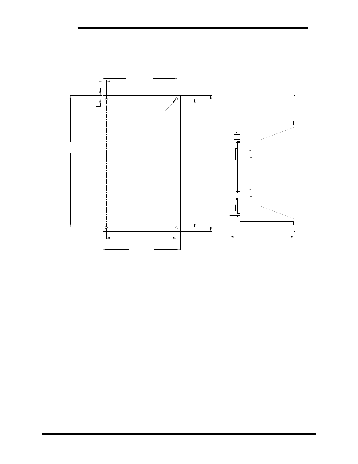
M3460
46
6.5. DIMENSIONS AND MECHANICAL DRAWINGS
Figure 6-1: M3460-R10 Chassis Dimensional Outline
13.45IN
[341.6MM]
MOUNTING FOOTPRINT
27.25IN
[692.2MM]
0.75IN
[19.0MM]
Ø0.50IN
[Ø12.7MM]
15.25IN
[387.4MM]
0.75IN
[19.0MM]
26.50IN
[673.1MM]
28.00IN
[711.2MM]
14.50IN
[368.3MM]
16.00IN
[406.4MM]
Page 47
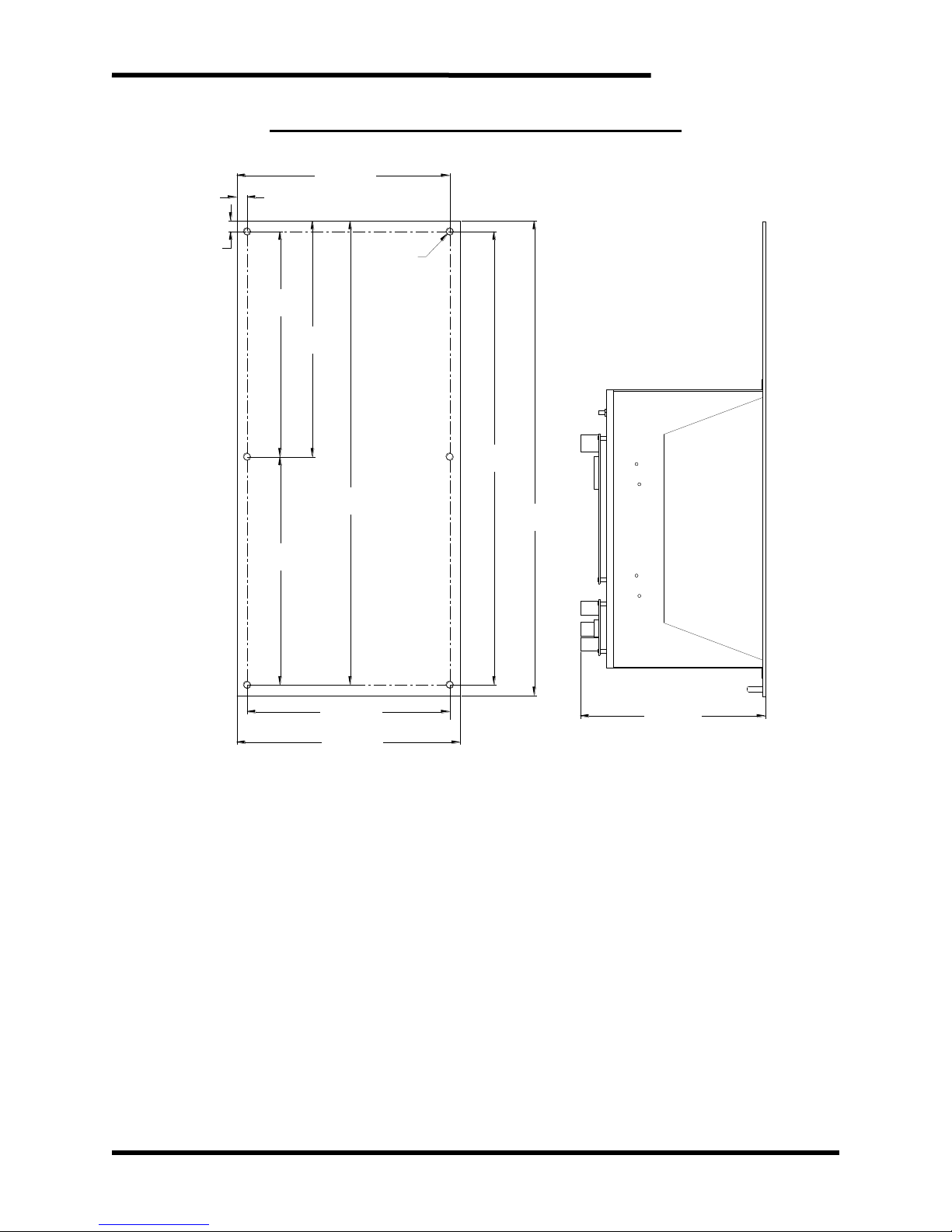
User’s Manual
47
Figure 6-2: M3460-R9 Chassis Dimensional Outline
13.25IN
[336.5MM]
16.15IN
[410.2MM]
Ø0.50IN
[Ø12.7MM]
MOUNTING FOOTPRINT
33.25IN
[844.6MM]
15.25IN
[387.4MM]
0.75IN
[19.0MM]
0.75IN
[19.0MM]
34.00IN
[863.6MM]
32.50IN
[825.5MM]
14.50IN
[368.3MM]
16.00IN
[406.4MM]
16.35IN
[415.3MM]
16.90IN
[429.3MM]
Page 48
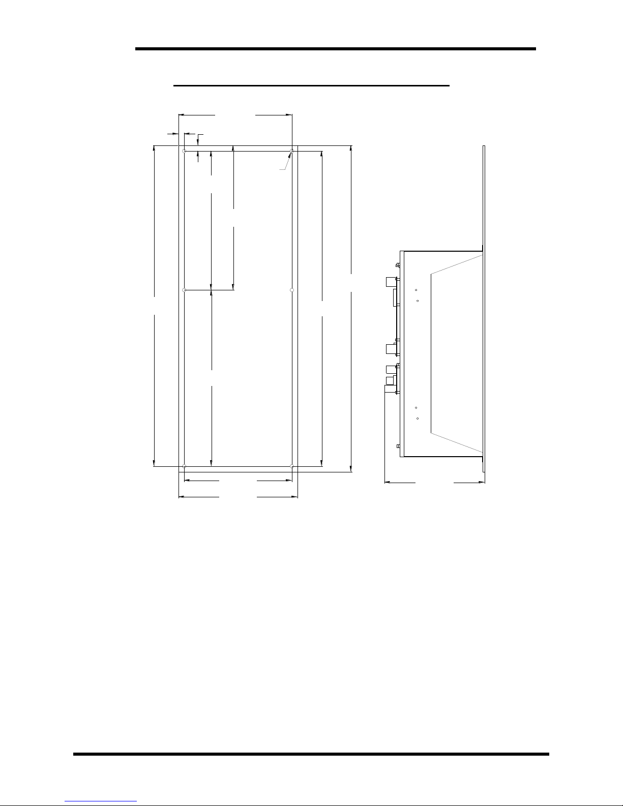
M3460
48
Figure 6-3: M3460-R11 Chassis Dimensional Outline
13.50IN
[342.9MM]
MOUNTING FOOTPRINT
19.50IN
[495.3MM]
43.25IN
[1098.6MM]
15.25IN
[387.4MM]
0.75IN
[19.0MM]
18.75IN
[476.2MM]
0.75IN
[19.0MM]
42.50IN
[1079.5MM]
44.00IN
[1117.6MM]
14.50IN
[368.3MM]
16.00IN
[406.4MM]
Ø0.50IN
[Ø12.7MM]
23.75IN
[603.2MM]
Page 49
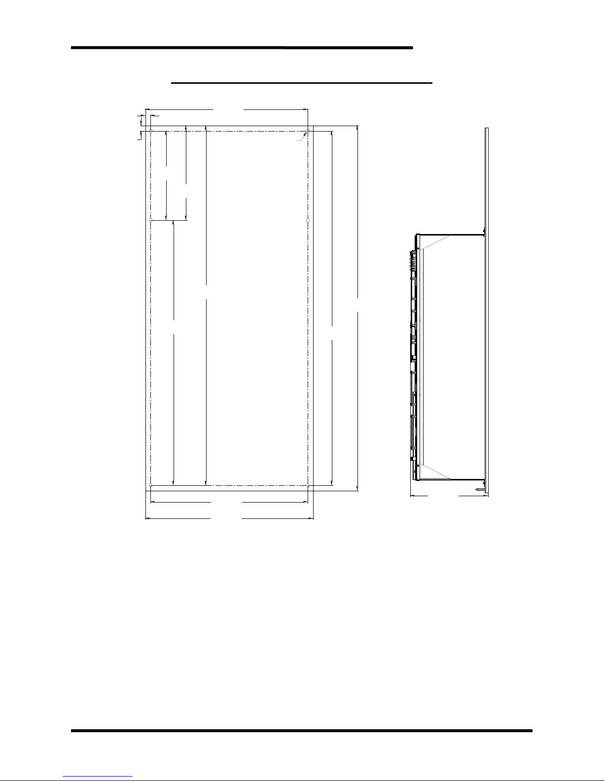
User’s Manual
49
Figure 6-4: M3460-R2 Chassis Dimensional Outline
0.75IN
[19.0MM]
0.75IN
[19.0MM]
12.75IN
[323.8MM]
13.50IN
[342.9MM]
51.25IN
[1301.8MM]
Ø0.50IN
[Ø12.7MM]
50.50IN
[1282.7MM]
52.00IN
[1320.8MM]
22.50IN
[571.5MM]
24.00IN
[609.6MM]
11.14IN
[283.0MM]
MOUNTING FOOTPRINT
37.75IN
[958.9MM]
23.25IN
[590.6MM]
Page 50
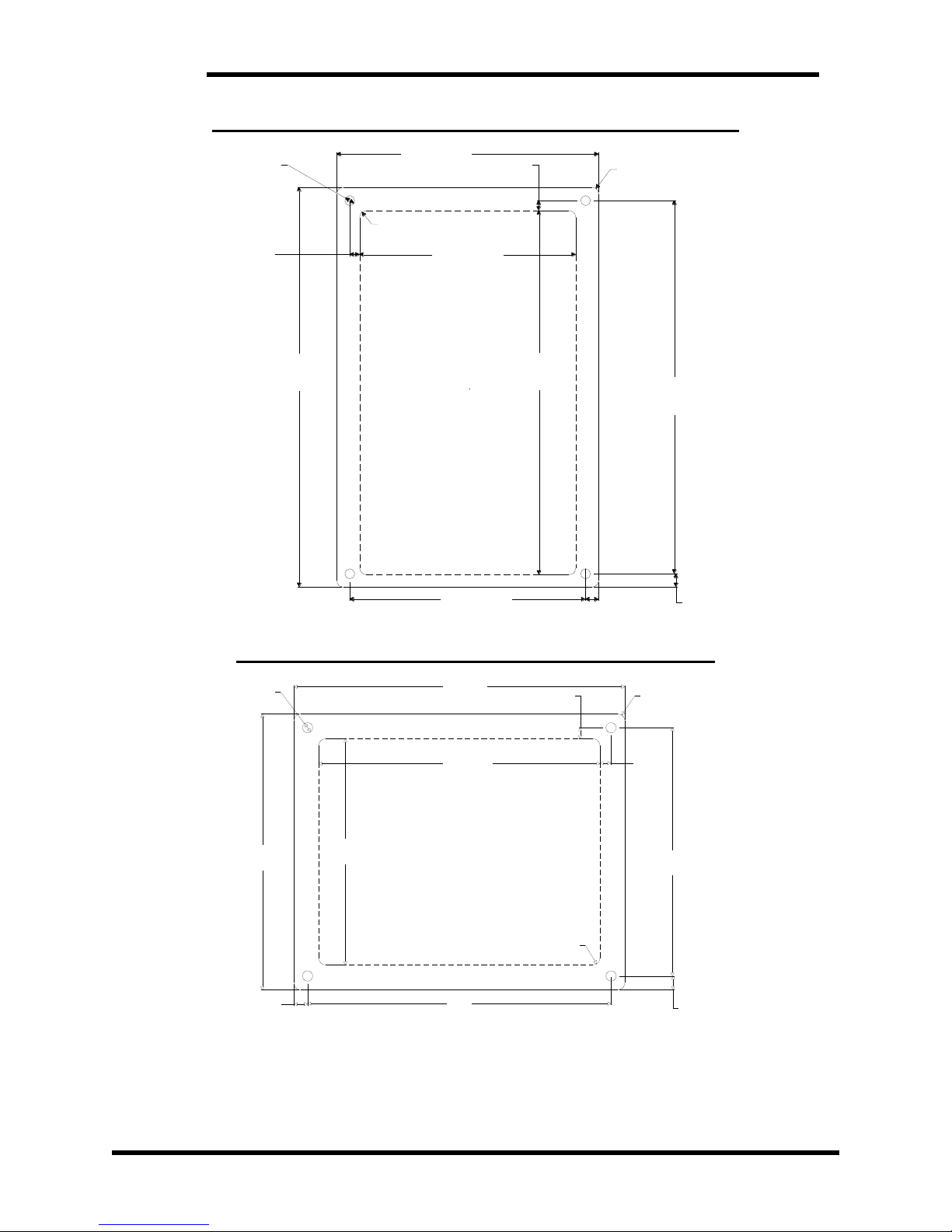
M3460
50
Figure 6-5: DD5 Digital Display Cutout and Mounting Dimensions
5.00
127.0 mm
7.50
190.5 mm
6.83
173.5 mm
4.13
104.8 mm
7.00
177.8 mm
.19
4.8 mm
4.50
114.3 mm
.25
6.4 mm
.25
6.4 mm
R.13
R3.2 mm
R.13
R3.2 mm
n.19
n4.8 mm
.19
4.8 mm
CUTOUT
Figure 6-6: DP10 Display Cutout and Mounting Dimensions
6.00
152.4mm
5.00
127mm
4.10
22.14mm
5.10
129.54mm
4x R.125
3.18mm
4x R.125
3.18mm
5.50
.25
6.35mm
4.50
114.3mm
.25
6.35mm
4x Ø.188
4.78mm
.20
5.08MM
.20
5.08MM
CUTOUT
Page 51
User’s Manual
51
7. APPENDICES
7.1. M3460 INSTALLATION CONSIDERATIONS
There are several things to take in to account when backing up a drive system. The
M3460 is designed to back up the power section of an AC drive, and does so within
the DC link of the drive.
DANGER!
MAKE SURE THE M3460R AND DRIVE HAVE THE SAME AC FEED, AS THE
M3460R WILL CONTINUE TO SUPPLY THE DRIVE WITH POWER IF BOTH SYSTEMS
ARE NOT TURNED OFF AT THE SAME TIME. LETHAL VOLTAGES EXIST IN THE
M3460R.
DANGER!
FOR SYSTEMS THAT HAVE BACKUP STORAGE SYSTEMS, SUCH AS CAPACITORS
OR BATTERIES, THE M3460 WILL CONTINUE TO SUPPLY POWER EVEN THOUGH
THE AC LINE IS DISCONNECTED! TAKE SPECIAL PRECAUTIONS WITH THESE
SYSTEMS TO ENSURE THAT THE POWER CAN BE REMOVED FROM THE SYSTEM
AND LETHAL VOLTAGES DRAINED OR DISCONNECTED FOR SERVICE!
1. The M3460 must have a DC bus connection directly to the DC bus filter
capacitors within the drives. Connections cannot be made through the braking
terminals or with precharge resistors or DC link chokes between the output of
the M3460 and the DC bus capacitors in the drive. Consult the manufacturers'
documentation or contact Bonitron for further assistance.
2. The drive system may depend on other parts of a larger control system that
requires backup to allow the drive to keep operating, like sensors or external
commands from PLC or relay logic. These systems will need to be backed up
separately with AC UPS systems or logic power backup systems like 24VDC
buffers.
3. Most drives have control and cooling power supplies that are connected to the
DC bus of the drive. These will be backed up by the M3460. Some larger frame
AC drives require consistent AC power to keep operating as they have fans
that get power directly from the AC line. In this case, there may be special
requirements to keep the drive operating.
4. Any AC line outage sensing must be disabled in the drive to keep the drive
from automatically shutting down on a phase loss.
5. Any kinetic buffering option needs to be disabled in the drive. This can cause
interference with the operation of the M3460.
6. If there is ground fault sensing within the drive, this may need to be disabled,
as uneven currents can flow through the AC drive's input bridge causing a trip.
7.2. SPECIFYING AN ULTRACAPACITOR STORAGE BANK FOR FULL OUTAGE
PROTECTION WITH M3460R MODELS
Bonitron M3460R models can have energy storage devices added to cover complete
outages. This involves adding a capacitor bank with an appropriate charging and
discharging system. Bonitron can source complete capacitor cabinets or individual
capacitors. This section gives some instruction for sizing and specifying these storage
devices.
The process described below is a good way to estimate the capacitor bank required.
Since the discharge characteristic of a capacitor bank with a constant power load is a
nonlinear differential equation, optimizing the capacitor bank selection is an iterative
Page 52

M3460
52
process. A general estimate of needs must be used to build a capacitor bank and then
the actual values must be cross checked to make sure they are suitable.
There are several steps in the process. The capacitor bank will be comprised of
capacitors connected in series for voltage support, with one or more strings in parallel
to support the energy requirements.
However, an additional power supply, the ASM 3460PS is required when the total
voltage across the ultracapacitor bank is lower than the Precharge Complete Voltage
(PCC). See Table 6-3 for the minimum PCC voltage required to bring the Ride-Thru
into operation.
Since the extraction losses due to the electrostatic resistance () of the capacitor
can be significant, they must be taken into account. If the losses get too high,
parallel capacitor strings can be used to reduce the current in each series string.
The steps to specify the string will include:
1. Determine the energy required for the outage.
2. Determine the minimum voltage acceptable for full power backup.
3. Determine the maximum current required to support the load at minimum
voltage.
4. Specify the capacitor to be evaluated.
5. Estimate the losses for each capacitor.
6. Determine the minimum number of capacitors per series string required for the
minimum voltage.
7. Add capacitors in series for outage energy.
8. Determine if parallel strings are required to provide outage energy.
These are the definitions of the variables we will use in the following equations:
- Capacitance at end of life
- Total capacitance of the entire cap bank
- Total equivalent ESR for the entire cap bank
- Internal resistance at end of life
- Peak current into the M3460R during the discharge cycle
- Total energy in charged capacitor bank prior to discharge
- Total losses during discharge
- Energy required to hold up the system during the outage
- Number of capacitors in each series string
- System power in kilowatts
- Time outage in seconds
- Charge voltage at beginning of discharge
- The capacitor string voltage at the end of the discharge
- Maximum charge voltage for the capacitor
- Lowest voltage the capacitor bank can reach
- Terminal voltage of an individual capacitor during discharge
Page 53

User’s Manual
53
7.2.1. ENERGY REQUIRED FOR OUTAGE
The total energy required for the event must be calculated first.
Using the following equation, the total number of joules required for the outage
can be calculated:
We will use a specification of 100 hp. for a 2 second outage for this example.
For instance, a 100 hp drive outage for 2 seconds would be
The total number of joules required is:
7.2.2. MINIMUM CAPACITOR BANK VOLTAGE
There is a minimum voltage level that must be maintained at the end of the
discharge during backup. An M3460R has, for a 460VAC nominal system, a
minimum input voltage of 320VDC. Therefore, the final discharge voltage of
the capacitor bank (
) should be 320 VDC.
These data are available in the specifications for the specific M3460R by
nominal system voltage.
7.2.3. PEAK CURRENT
The peak current from the capacitor bank will occur at the minimum voltage.
This can be estimated from the equation
For our example,
7.2.4. CAPACITOR SPECIFICATIONS
At this point, a specific capacitor's characteristics can be used. It is best to use
the values that are listed at end of life for the capacitor to make sure that the
storage system is sized for the eventual degradation of performance over time.
The critical points to use are
= Internal resistance at end of life, typically 150-200% of the initial
value.
= Capacitance at end of life
= Maximum charge voltage for the capacitor. (A general rule is to use
95% of the value listed on the datasheet for a reasonable margin)
For our example, we will use the following values:
Page 54

M3460
54
= .01Ω
= 132F
= 46V
7.2.5. MINIMUM SERIES STRING
From
, we can calculate the minimum series string of capacitors that
will be required by the voltage rating. Below this voltage, there is an amount of
stored energy that cannot be used, and will remain in the capacitor bank. Since
there can be significant terminal voltage drop at the end of the discharge cycle
due to , it is best to use the terminal voltage of the capacitors (
for
this calculation.
For our example, the minimum number of caps in a series string would be:
7.2.6. AVAILABLE JOULES
At this point, the available maximum joules for the string can be calculated.
The capacitor voltage at the end of the discharge
will be given by:
The total capacitance of the series string is given by:
Now, the total energy that can be delivered to the load is given by:
The equivalent of the string is given by
Page 55

User’s Manual
55
The total extraction losses of the string is given by
Now the total required energy can be compared.
This combination of capacitors will be adequate for our example application.
If the application required more energy, then capacitors can be added in series,
and the calculations redone as in 7.3.1. If the charge voltage exceeds the
maximum input voltage for the M3460R, then the minimum series string
combination should be used in parallel and the process repeated.
7.3. STEERING DIODE SHARING WITH A BONITRON M3460 RIDE-THRU
Diode sharing is used to decrease the cost of implementing M3460 modules to existing
drive systems that are not common bussed. The use of diodes will prevent drive
busses from “back feeding” each other, by allowing energy to pass one way only. This
can be useful to keep the bridge from one drive feeding other drives and becoming
overloaded during normal operations.
For Ride-Thru applications, the energy is allowed to pass from the M3460 to the drives,
but is blocked from the drives to the M3460. Figure 7-1 is a block diagram of a diode
sharing example.
Below are some basic guidelines for using diodes in this manner for M3460
applications.
1. In general, it’s best to use drives from a common manufacturer and series of
drives. Questions about the suitability of combining drives can be answered by
the drive manufactures.
2. Drives must be on same AC feed and grounding. There must be no isolation
transformers between the drives or M3460 modules. Different feeds may have
different potentials and may cause circulating currents or ground faults.
3. If line chokes or harmonic filters are used, all the drives should be connected to
the output of a single choke or filter. Individual input harmonic filters or line
chokes can cause unequal potentials with respect to earth.
4. The M3460 connection should be downstream of any input line filter. Input line
filters cause lower DC bus levels. If a M3460 is placed upstream, the Ride-Thru
DC bus can be higher than the drive bus, and current can flow through the M3460
during normal operation. This can cause constant activity and overheating. It
may be necessary to lower the threshold for these applications.
Page 56
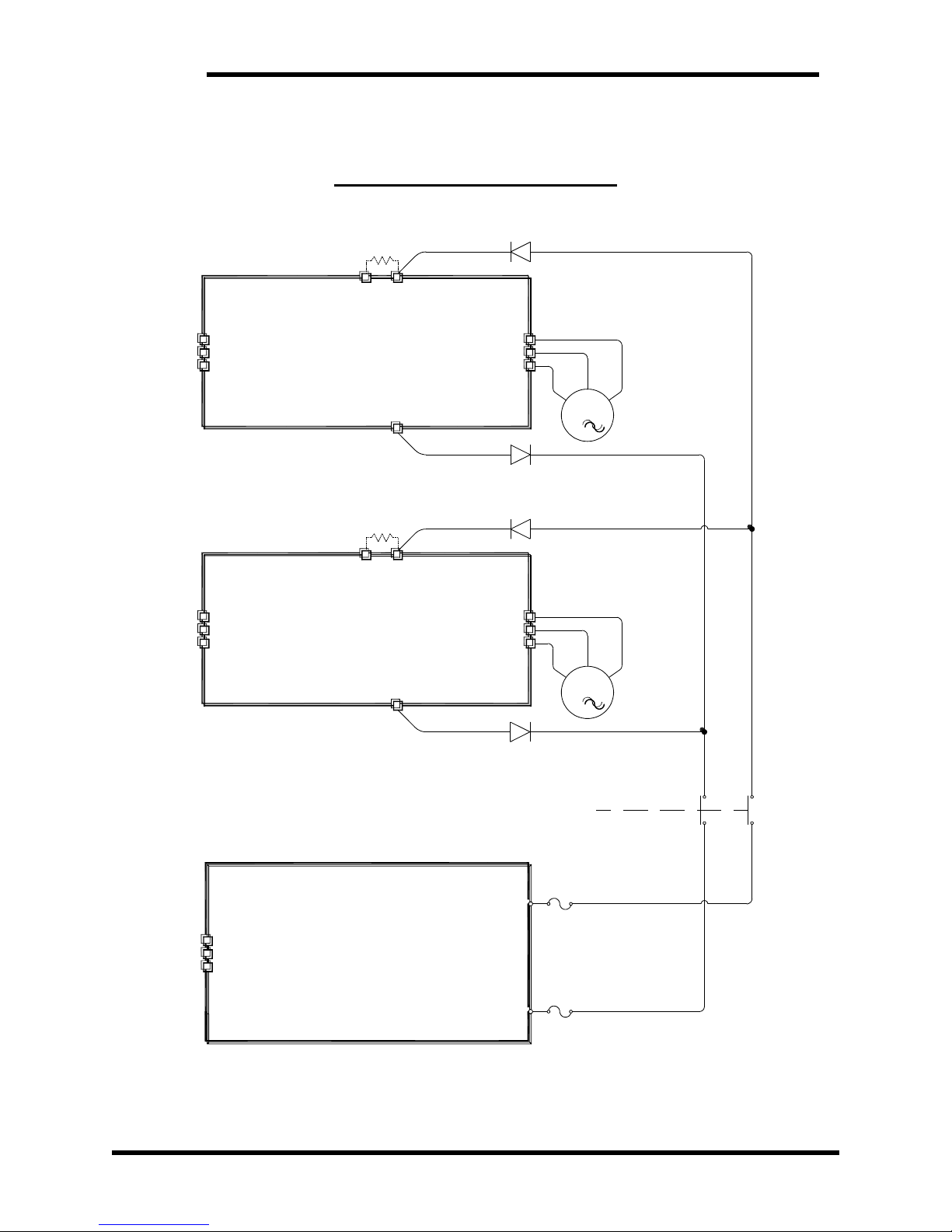
M3460
56
5. Ground Fault sensing should be done upstream at common point of line
connection.
Figure 7-1: Diode Sharing Example
VFD
BRAKING
RESISTOR
DISCONNECT
DC BUS
MODEL M3460/M3534
+
-
DC
OUTPUT
M
3
VFD
BRAKING
RESISTOR
M
3
Page 57
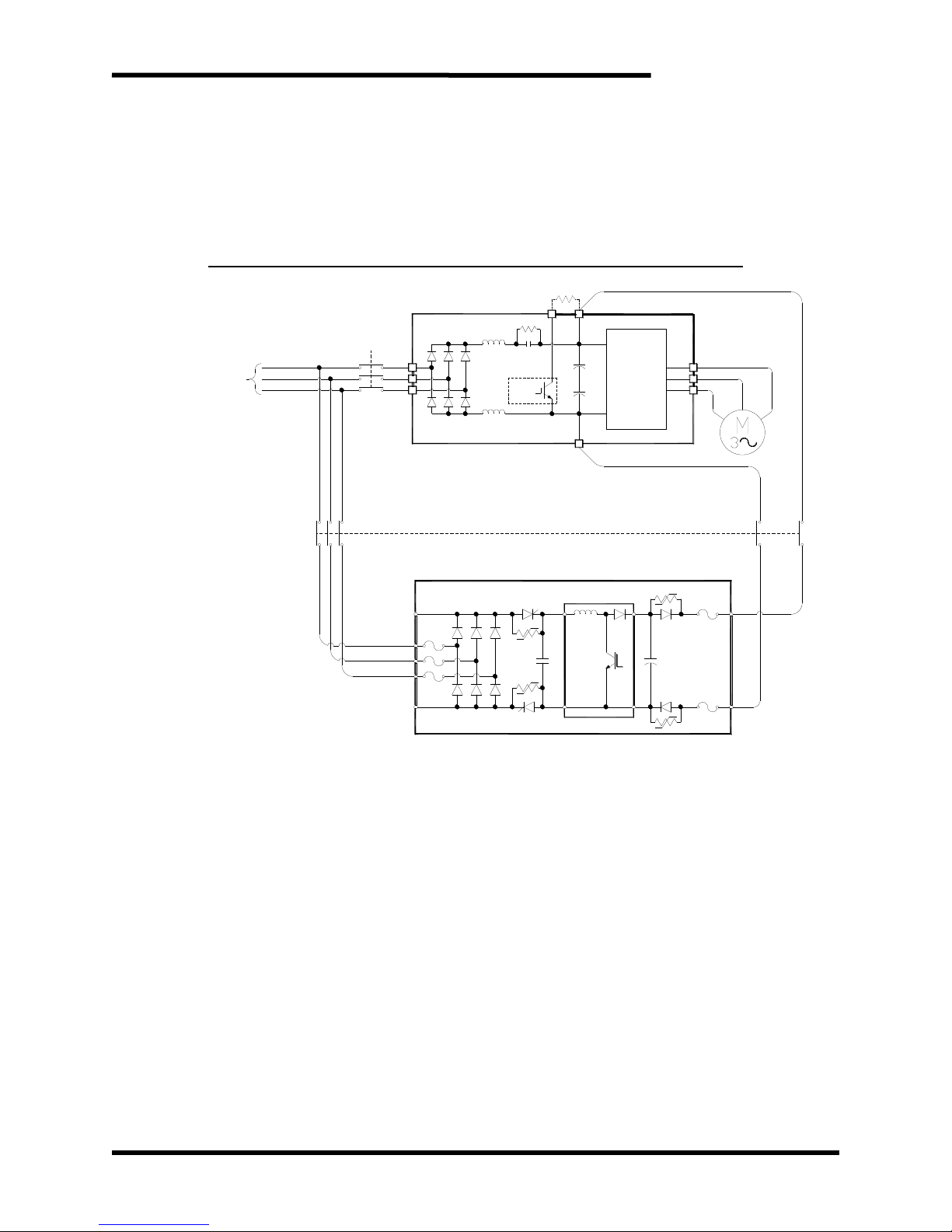
User’s Manual
57
7.4. SAG ONLY INSTALLATIONS & CIRCULATING CURRENTS
The topology of the M3460R voltage boost module incorporates a six diode full wave
three phase rectifier bridge. When the M3460R is connected to the DC bus of the
variable frequency drive, the input rectifier bridge of the variable frequency drive is in
parallel with the M3460R input rectifier bridge. There are two diodes in parallel from
the DC bus to the AC line for each connection.
Figure 7-2: M3460R Typical Configuration without Energy Storage
CHOPPER
BRAKING
INTERNAL
VFD
INVERTER
BRAKING
RESISTOR
DISCONNECT
DRIVE
DISCONNECT
RIDE-THRU
M3460R
CHOPPER
+
-
+
-
DRIVE
BUS
STORAGE BUS
STORAGE BUS
AC
FEED
Page 58
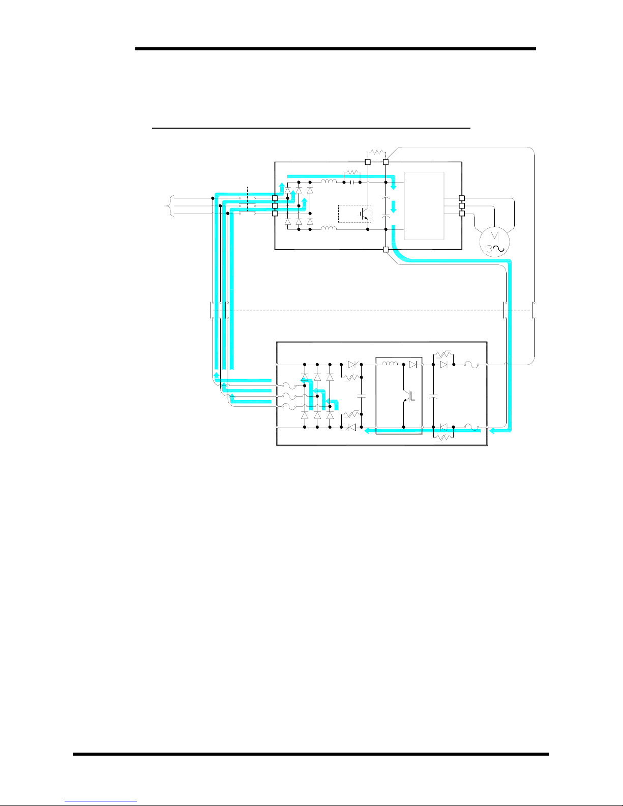
M3460
58
The current will follow the path with the least resistance, this can cause “circulation
currents”, or currents that may enter the DC bus of the M3460R through one bridge
and return to the AC source through the other bridge.
Figure 7-3: M3460R Typical Configuration with Current Flow
CHOPPER
BRAKING
INTERNAL
VFD
INVERTER
BRAKING
RESISTOR
DISCONNECT
DRIVE
DISCONNECT
RIDE-THRU
M3460R
CHOPPER
+
-
+
-
DRIVE
BUS
STORAGE BUS
STORAGE BUS
AC
FEED
Page 59
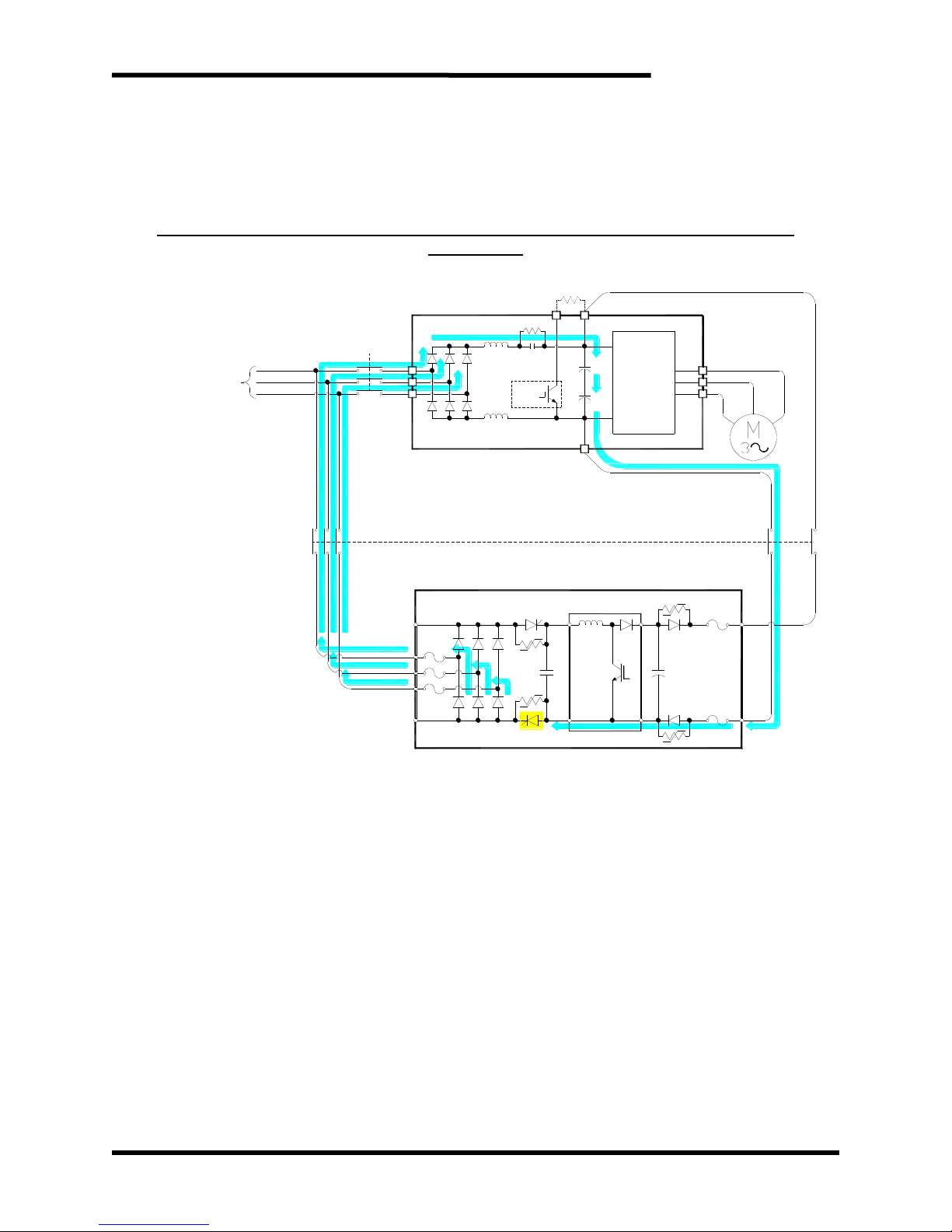
User’s Manual
59
If the circulation current shown above in Figure 7-2 is established and remains during
standby operation, the highlighted SCR/Thyristor in Figure 7-3 can remain on and
overheat due to the continuous current flow.
If the circulating current situation is not corrected the SCR may be permanently
damaged and fail.
Figure 7-3: M3460R Typical Configuration with Current Flow with affected SCR
Highlighted
CHOPPER
BRAKING
INTERNAL
VFD
INVERTER
BRAKING
RESISTOR
DISCONNECT
DRIVE
DISCONNECT
RIDE-THRU
M3460R
CHOPPER
+
-
+
-
DRIVE
BUS
STORAGE BUS
STORAGE BUS
AC
FEED
In order to prevent this situation, extra impedance should be added to the negative
connection of the ride-thru to the drive. This prevents the circulation current from being
sustained after a sag event.
The M3460RD is not required in all installations, however determining the requirement
is difficult due to the variables involved with the physical installation. Using the
M3460RD does not reduce the Ride-Thru capacity for the system, and is
recommended for all installations.
Please note that this situation can only occur when there is an AC connection to the
input bridge of the M3460R unit. If the installation contains energy storage, such as
capacitors, the two input bridges are galvanically isolated from each other by the
isolation transformer of the charging system. In this case, the M3460RD is not
required. See Figure 7-4 for an example of a galvanically isolated system.
Page 60
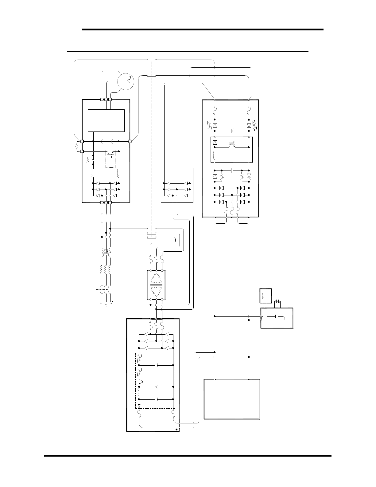
M3460
60
Figure 7-4: M3460R Typical Configuration with Ultracapacitor Storage Bank
KIT 3628T
DISCHARGER
M3628R
CHOPPER
BRAKING
INTERNAL
VFD
INVERTER
BRAKING
RESISTOR
DISCONNECT
DRIVE
FEED
AC
CHOKES
LINE
GROUND
FAULT
SENSING
M3528AC CHARGER
ULTRA CAP
ENERGY STORAGE
BANK
DISCONNECT
RIDE-THRU
M3460R
CHOPPER
+
-
+
-
+
-
DRIVE
RIDE-THRU
DISCONNECT
AUX. CONTACT
BUS
STORAGE BUS
STORAGE BUS
M
3
ISOLATION TRANSFORMER
FROM THE SAME FEED TRANSFORMER.
CONNECTED DOWNSTREAM.
2. IF LINE CHOKES ARE USED, RIDE-THRU MUST BE
1. INVERTER AND RIDE-THRU SHOULD BE POWERED
~NOTES~
+
-
L1
L2
ASM 3460PS
IS LOWER THAN PCC VOLTAGE.
3. ASM 3460 PS WILL BE USED IF THE INPUT DC LEVEL
*OPTIONAL: SEE SECTION 7.2
Page 61

User’s Manual
61
NOTES
Page 62

M3460
62
Page 63

Page 64

D_M3460 _CMAN_vall_01a 02/20/2018
521 Fairground Court ● Nashville, TN 37211 ● USA
 Loading...