

BOE HV550WU2-200 Specification
TITLE:
PROPRIETARY NOTE
THIS SPECIFICATION IS THE PROPERTY OF BOE DT AND SHALL NOT BE
REPRODUCED OR COPIED WITHOUT THE WRITTEN PERMISSION OF BOE DT
AND MUST BE RETURNED TO BOE DT UPON ITS REQUEST
HV550WU2-200 Product Specification
SPEC. NUMBER
S865-8A058
B2010-8002-O (1/3)
BEIJING BOE DISPLAY TECHNOLOGY
PRODUCT GROUP
TFT LCD
REV.
O
ISSUE DATE
2013.06.17
PAGE
of 25
1
A4(210 X 297)
A4(210 X 297)
PRODUCT GROUP
REVISION HISTORY
REV ISSUE DATE
TFT LCD
O 2013.06.17
REV. ECN NO. DESCRIPTION OF CHANGES DATE PREPARED
O - Initial Release 2013.06.17 LI XIANG
SPEC. NUMBER
S865-8A058
B2010-8002-O (2/3)
SPEC. TITLE
HV550WU2-200 Product Specification
PAGE
of 25
2
A4(210 X 297)
PRODUCT GROUP
3.1 TFT LCD Modul
g
REV ISSUE DATE
TFT LCD
O 2013.06.17
Contents
No ITEM Page
REVISIONS HISTORY 2
CONTENTS
1 GENERAL DESCRIPTION
1.1 Introduction
1.2 Features
1.3 Applications
1.4 General Specification
2 ABSOLUTE MAXIMUM RATINGS 6
3 ELECTRICAL SPECIFICATIONS 7
e
4 INTERFACE CONNECTION 8
3
4
4.1 Module Input Signal & Power
4.2 LVDS Interface
5 SIGNAL TIMING SPECIFICATIONS
5.1 Timing Parameters
5.2 Signal Timing Waveform
5.3 Input Signals, Basic Display Colors & Cray Scale Of Colors
5.4 Power Sequence
6 OPTICAL SPECIFICATIONS 15
7 MECHANICAL CHARACTERISTICS 18
8 RELIABLITY 29
9 PRODUCT SERIAL NUMBER 20
10 PACKING INFORMATION 21
11 HANDING & CAUTIONS 23
12 APPENDIX
11
24
SPEC. NUMBER
S865-8A058
B2010-8002-O (3/3)
SPEC. TITLE
HV550WU2-200 Product Specification
PAGE
of 25
3
A4(210 X 297)
PRODUCT GROUP
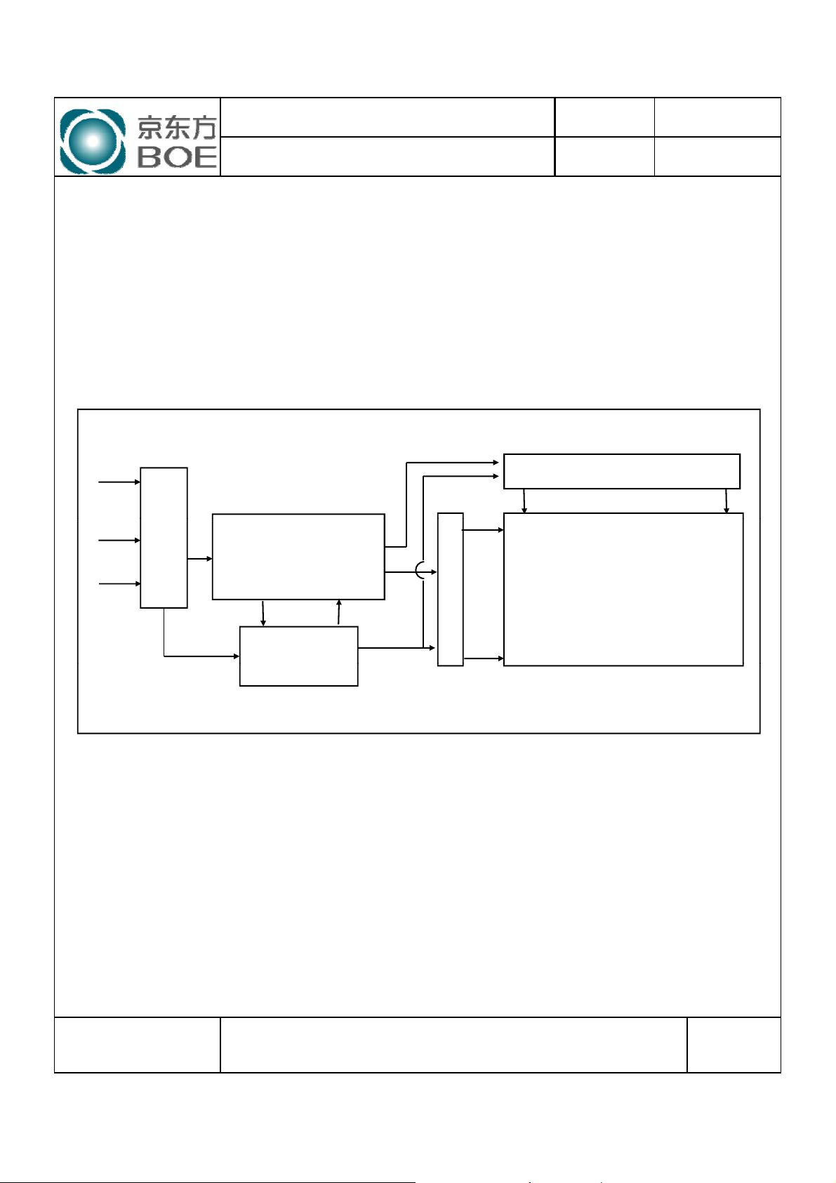
G1
Block
z
LVDS interf
ith 2 pixel / clock
ADS
REV ISSUE DATE
TFT LCD
O 2013.06.17
1.0 GENERAL DESCRIPTION
1.1 Introduction
HV550WU2-200 is a color active matrix TFT LCD open cell using amorphous silicon TFT's
(Thin Film Transistors) as an active switching devices. This open cell has a 54.6inch
diagonally measured active area with WUXGA resolutions (1920 horizontal by 1080
vertical pixel array). Each pixel is divided into RED, GREEN, BLUE dots which are
arranged in vertical stripe and this open cell can display 16.7M colors. The TFT-LCD panel
used for this open cell is adapted for a low reflection and higher color type.
RGB(Mini-LVDS)
VDD
+12.0V
LVDS
2Ports
LVDS_SEL
# 7
CN1
(51pin)
S1 S1920
Gate Driver Circuit
Timing Controller
[LVDS Rx & Mini-LVDS
Tx integrated]
Source Driver Circuit
TFT - LCD Panel
(1920 × RGB × 1080 pixels)
Power Circuit
G1080
1.2 Features
ace w
z High-speed response
z Low color shift image quality
z 8-bit color depth, display 16.7M colors
z High luminance and contrast ratio, low reflection and wide viewing angle
z DE (Data Enable) only mode
z
z RoHS compliant
SPEC. NUMBER
technology is applied for high display quality
SPEC. TITLE
S865-8A058
HV550WU2-200 Product Specification
PAGE
of 25
4
B2010-8002-O (3/3)
A4(210 X 297)
PRODUCT GROUP
Display colors
16.7M(8bits
true)
colors
REV ISSUE DATE
TFT LCD
1.3 Application
z Home Alone Multimedia TFT-LCD TV
z Display Terminals for Control System
z Full High Definition TV(FHD TV)
z AV application Products
1.4 General Specification
< Table 1. General Specifications >
Parameter Specification Unit Remark
Active area
1209.6(H) × 680.4(V)
O 2013.06.17
mm Array
Number of pixels
Pixel pitch
Pixel arrangement Pixels RGB Vertical stripe Array
Display mode Transmission mode, Normally Black
Open Cell
Transmittance
Power Consumption 9.0W(typ.)
Surface Treatment Haze 1%, 2H, Anti-glare treatment (Front
1920(H) ×1080(V)
630(H) ×630(V) ㎛
-
6.7 (typ.) %
Polarizer)
pixels
Array
At center
point with
BOE BLU
Watt
SPEC. NUMBER
S865-8A058
B2010-8002-O (3/3)
SPEC. TITLE
HV550WU2-200 Product Specification
PAGE
of 25
5
A4(210 X 297)
PRODUCT GROUP
Parameter
Symbol
Min
Max
Unit
Remark
O
Wet bulb temperature should be 39
℃
max. and no condensation of water
Wet Bulb
R
REV ISSUE DATE
TFT LCD
O 2013.06.17
2.0 ABSOLUTE MAXIMUM RA TINGS
The followings are maximum values which, if exceed, may cause faulty operation or
damage to the unit. The operational and non-operational maximum voltage and current
values are listed in Table 2.
< Table 2. LCD Open Cell Electrical Specifications >
.
.
Power Supply Voltage VDD VSS-0.3 13.5 V
T
Operating Temperature
T
Storage Temperature T
perating Ambient
Humidity
Hop 10 80 %RH
OP
SUR
ST
0+50
0+60
-20 +60
℃
℃
℃
[VSS=GND=0V]
Ta = 25 ℃
Note 1
Storage Humidity Hst 10 80 %RH
Note 1 : Temperature and relative humidity range are shown in the figure below.
Temperature [C]
10
0
10 20 30 40 50 60 70 800-20
Dry Bulb Temperature [
20
30
40
°C]
50
80%
60
60%
H]
40%
Humidity [(%)
10%
.
Storage
Operation
SPEC. NUMBER
S865-8A058
B2010-8002-O (3/3)
SPEC. TITLE
HV550WU2-200 Product Specification
PAGE
of 25
6
A4(210 X 297)
PRODUCT GROUP
LVDS
VIL0-
0.6
V
REV ISSUE DATE
TFT LCD
O 2013.06.17
3.0 ELECTRICAL SPECIFICATIONS
3.1 TFT LCD Open Cell
< Table 3. LCD Open Cell Electrical Specifications >
Values
Parameter Symbol
Min Typ Max
Power Supply Input Voltage VDD 10.8 12 13.2 Vdc
Power Supply Ripple Voltage VRP 300 mV
Power Supply Current IDD 700 mA
Power Consumption PDD 9.0 Watt
Rush current IRUSH 4 A Note 2
Differential Input High
VLVTH +100 +300 mV
Threshold Voltage
Interface
Differential Input Low
Threshold Voltage
VLVTL -300 -100 mV
[Ta =25±2 ℃]
Unit Remark
Note 1
Common Input Voltage VLVC 1.0 1.2 1.4 V
Input High Threshold
VIH 2.7 - 3.3 V
CMOS
Interface
Voltage
Input Low Threshold
Voltage
Note 1 : The supply voltage is measured and specified at the interface connector of LCM.
The current draw and power consumption specified is for VDD=12.0V,
Frame rate f
Test Pattern of power supply current
a) Typ : Color Test (L0/L255) b) Max : Vertical Subline (L0/L255)
Note 2 : The duration of rush current is about 2ms and rising time of Power Input is 1ms(min)
=60Hz and Clock frequency = 75.4MHz.
V
SPEC. NUMBER
S865-8A058
B2010-8002-O (3/3)
SPEC. TITLE
HV550WU2-200 Product Specification
PAGE
of 25
7
A4(210 X 297)
PRODUCT GROUP
3
SCL
I2C Clock
28
CH2[0]
Second pixel negative LVDS
3
CH1[0]
38
CH2[3]
13
CH1[0]
diff
0
38
CH2[3]
18
GND
43
NC
p
p
REV ISSUE DATE
TFT LCD
O 2013.06.17
4.0 INTERF ACE CONNECTION
4.1 Open Cell Input Signal & Power
- Connector : FW05010-51(Manufactured by FOOSUNG) or Equivalent.
< Table 5. Open Cell Input Connector Pin Configuration >
Pin No
1 NC No Connection 26 2D/3D 2D/3D Signal Select
2SDA I
4 WP nWR(PGAMA data write protect) 29 CH2[0]+
5 NC 30 CH2[1]- “
6 NC 31 CH2[1]+ “
7 SELLVDS
8 NC 33 CH2[2]+ “
9NC 34GND
10 NC 35 CH2CLK- First pixel negative LVDS clock
11 GND 36 CH2CLK+ First pixel positive LVDS clock
12 CH1[0]-
1
14 CH1[1]- “ 39 CH2[3]+ “
15 CH1[1]+ “ 40 CH2[4]-/NC
16 CH1[2]- “ 41 CH2[4]+/NC
17 CH1[2]+ “ 42 NC
Symbol Description
2
C Data 27 L/R Left Right Eye Frame Sync.
High or Openh: NS
Low: JEIDA
First pixel negative LVDS
differential data input. Pair0
+
First pixel positive LVDS
erential data input. Pair
Pin No
32 CH2[2]- “
37 GND
Symbol Description
-
-“
differential data input. Pair0
Second pixel positive LVDS
differential data input. Pair0
Second pixel negative LVDS
differential data input. Pair0
Second pixel positive LVDS
differential data input. Pair0
19 CH1CLK- First pixel negative LVDS clock 44 GND Ground
20 CH1CLK+ First pixel positive LVDS clock 45 GND “
21 GND 46 GND “
22 CH1[3]- 47 NC “
23 CH1[3]+ 48 VCC Input Voltage
24 CH1[4]-/NC
25 CH1[4]+/NC
SPEC. NUMBER
S865-8A058
B2010-8002-O (3/3)
First pixel negative LVDS
differential data in
First pixel positive LVDS
differential data input. Pair0
ut. Pair0
49 VCC “
50 VCC “
51 VCC “
SPEC. TITLE
HV550WU2-200 Product Specification
PAGE
of 25
8
A4(210 X 297)
 Loading...