

BOE HV320WXC-211 Specification
Global LCD Panel Exchange Center
THIS SPECIFICATION IS THE PROPERTY OF BOE DT AND SHALL NOT BE
REPRODUCED OR COPIED WITHOUT THE WRITTEN PERMISSION OF BOE DT AND
MUST BE RETURNED TO BOE DT UPON ITS REQUEST
TITLE :
www.panelook.com
PROPRIETARY NOTE
HV320WXC-211
Product Specification
Rev. 0
SPEC. NUMBER
S8-64-8A-011
One step solution for LCD / PDP / OLED panel application: Datasheet, inventory and accessory!
PRODUCT GROUP
TFT-LCD
REV.
0
ISSUE DATE
2012.03.29
PAGE
OF 26
X
A4(210 X 297)
www.panelook.com
Global LCD Panel Exchange Center
www.panelook.com
PRODUCT GROUP
TFT- LCD PRODUCT
REV
0 2012.03.29
ISSUE DATE
REVISION HISTORY
REV. ECN NO. DESCRIPTION OF CHANGES DATE PREPARED
0 Initial Release 2012.03.29 Zhang HL
SPEC. NUMBER
z_T][T_hTWXX
One step solution for LCD / PDP / OLED panel application: Datasheet, inventory and accessory!
SPEC. TITLE
HV320WXC-211 Product Specification Rev.0
PAGE
OF 26
2
A4(210 X 297)
www.panelook.com
Global LCD Panel Exchange Center
www.panelook.com
PRODUCT GROUP
TFT- LCD PRODUCT
REV
0
ISSUE DATE
Contents
No ITEM Page
REVISIONS HISTORY 2
CONTENTS
1 GENERAL DESCRIPTION
1.1 Introduction
1.2 Features
1.3 Applications
1.4 General Specification
2 ABSOLUTE MAXIMUM RATINGS 6
2012.03.29
3
4
3 ELECTRICAL SPECIFICATIONS 7
3.1 TFT LCD Module
4 INTERFACE CONNECTION 8
4.1 Module Input Signal & Power
4.2 LVDS Interface
4.3 LED Light Bar input Power
5 SIGNAL TIMING SPECIFICATIONS
5.1 Timing Parameters
5.2 Signal Timing Waveform
5.3 Input Signals, Basic Display Colors & Cray Scale Of Colors
5.4 Power Sequence
6 OPTICAL SPECIFICATIONS 15
7 MECHANICAL CHARACTERISTICS 17
8RELIABLITY
11
18
9 PRODUCT SERIAL NUMBER 19
10 PACKING INFORMATION
11 HANDING & CAUTIONS 21
12 APPENDIX
SPEC. NUMBER
S8-64-8A-011
One step solution for LCD / PDP / OLED panel application: Datasheet, inventory and accessory!
SPEC. TITLE
HV320WXC-211 Product Specification Rev.0
20
22
PAGE
3
OF 26
A4(210 X 297)
www.panelook.com
Global LCD Panel Exchange Center
www.panelook.com
PRODUCT GROUP
TFT- LCD PRODUCT
REV
0
ISSUE DATE
2012.03.29
1.0 GENERAL DESCRIPTION
1.1 Introduction
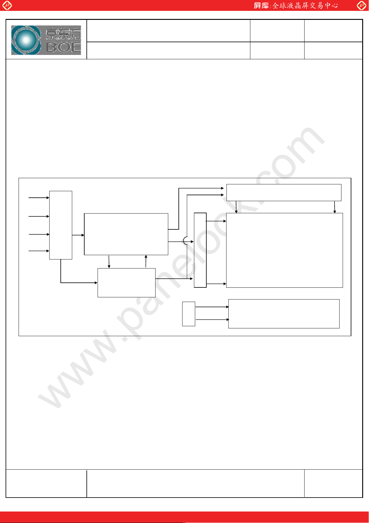
HV320WXC-211 is a color active matrix TFT LCD module using amorphous silicon TFT's
(Thin Film Transistors) as an active switching devices. This module has a 31.51 inch diagonally
measured active area with WXGA resolutions (1366 horizontal by 768 vertical pixel array).
Each pixel is divided into RED, GREEN, BLUE dots which are arranged in vertical stripe and
this module can display 16.7M colors. The TFT-LCD panel used for this module is adapted for a
low reflection and higher color type.
RGB(Mini-LVDS)
VDD
+12.0V
LVDS
5pairs
LVDS_SEL
# 9
BIST_
# 27
CN1
(30pin)
Timing Controller
[LVDS Rx & Mini-LVDS
Tx integrated]
Gate Driver Circuit
S1 S1366
G1
Source Driver Circuit
TFT - LCD Panel
(1366 Ý RGB Ý 768 pixels)
Power Circuit
Block
CN
1.2 Features
z LVDS interface with 1 pixel / clock
z High-speed response
z Low color shift image quality
z 8-bit color depth, display 16.7M colors
z High luminance, low reflection and wide viewing angle
z DE (Data Enable) only mode
z iFFS technology is applied for high display quality
G768
Back light Assembly
z RoHS compliant
SPEC. NUMBER
S8-64-8A-011
One step solution for LCD / PDP / OLED panel application: Datasheet, inventory and accessory!
SPEC. TITLE
HV320WXC-211 Product Specification Rev.0
PAGE
4
OF 26
A4(210 X 297)
www.panelook.com
Global LCD Panel Exchange Center
www.panelook.com
PRODUCT GROUP
TFT- LCD PRODUCT
1.3 Application
z Home Alone Multimedia TFT-LCD TV
z Display Terminals for Control System
z High Definition TV(HD TV)
z AV application Products
1.4 General Specification
< Table 1. General Specifications >
REV
0
ISSUE DATE
2012.03.29
Parameter Specification Unit Remarks
Active area 697.685(H) Ý 392.256(V) mm
Number of pixels 1366(H) ശ768(V) pixels
Pixel pitch 170.25(H) ശRGBശ510.75(V)
Pixel arrangement Pixels RGB Vertical stripe
Display colors 16.7M(8bits-true) colors
Display mode Transmission mode, Normally Black
Outline Dimension 727.4(H) Ý 429(V) Ý 9.9(Body) typ. mm
Weight 5.2kg(max) gram
Power Consumption
Surface Treatment Haze 10%, 3H, Semi-glare treatment (Front
Total=35.2.0Watt (Typ.)
(Logic=4.0W, BL=31.2W )
Polarizer)
ໃ
Watt
SPEC. NUMBER
S8-64-8A-011
One step solution for LCD / PDP / OLED panel application: Datasheet, inventory and accessory!
SPEC. TITLE
HV320WXC-211 Product Specification Rev.0
PAGE
5
OF 26
A4(210 X 297)
www.panelook.com
Global LCD Panel Exchange Center
www.panelook.com
PRODUCT GROUP
TFT- LCD PRODUCT
REV
0
2.0 ABSOLUTE MAXIMUM RATINGS
The followings are maximum values which, if exceed, may cause faulty operation or
damage to the unit. The operational and non-operational maximum voltage and current
values are listed in Table 2.
< Table 2. LCD Module Electrical Specifications >
Parameter Symbol Min. Max. Unit Remarks
Power Supply
Voltage
Operating Temperature
LCD Module VDD VSS-0.3 13.2 V
T
OP
0+50
ଇ
ISSUE DATE
2012.03.29
[VSS=GND=0V]
Ta = 25 ଇ
T
Storage Temperature T
SUR
ST
0+70
-20 +60
ଇ
ଇ
Operating Ambient Humidity Hop 10 80 %RH
Storage Humidity Hst 10 80 %RH
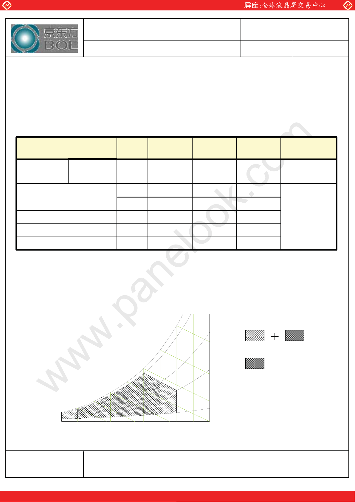
Note 1 : Temperature and relative humidity range are shown in the figure below.
Wet bulb temperature should be 39 ఁ max. and no condensation of water.
ړڋڀ
ڑڋ
ڑڋڀ
ڲۀۏٻڝېۇڽ
گۀۈۋۀۍڼۏېۍۀٻڶڞڸ
ڎڋ
ڍڋ
ڌڋ
ڋ
ڐڋ
ڏڋ
ڏڋڀ
ڣېۈۄڿۄۏ۔ٻڶڃڀڄڭڣڸ
ڌڋڀ
Note 1
ڮۏۊۍڼۂۀ
ڪۋۀۍڼۏۄۊۉ
ڌڋ ڍڋ ڎڋ ڏڋ ڐڋ ڑڋ ڒڋ ړڋڋڈڍڋ
ڟۍ۔ٻڝېۇڽٻگۀۈۋۀۍڼۏېۍۀٻڶ
SPEC. NUMBER
S8-64-8A-011
One step solution for LCD / PDP / OLED panel application: Datasheet, inventory and accessory!
SPEC. TITLE
HV320WXC-211 Product Specification Rev.0
¶Cڸ
PAGE
6
OF 26
A4(210 X 297)
www.panelook.com
Global LCD Panel Exchange Center
www.panelook.com
PRODUCT GROUP
TFT- LCD PRODUCT
REV
0
3.0 ELECTRICAL SPECIFICATIONS
3.1 TFT LCD Module
< Table 3. LCD Module Electrical Specifications >
Values
Parameter Symbol
Min Typ Max
Power Supply Input Voltage VDD 10.8 12 13.2 Vdc
Power Supply Ripple Voltage VRP 300 mV
Power Supply Current IDD -
Power Consumption PDD
333 592
4.0 7.1
ISSUE DATE
2012.03.29
[Ta =25ധ2 ଇ]
Unit Notes
mA
1
Watt
Rush current IRUSH - - 3.0 A 2
Differential Input High
VLVTH +100 +300 mV
Threshold Voltage
LVDS
Interface
Differential Input Low
VLVTL -300 -100 mV
Threshold Voltage
Common Input Voltage VLVC 1.0 1.2 1.4 V
Input High Threshold
VIH 2.7 - 3.3 V
CMOS
Interface
Voltage
Input Low Threshold
VIL 0 - 0.6 V
Voltage
Notes : 1. The supply voltage is measured and specified at the interface connector of LCM.
The current draw and power consumption specified is for VDD=12.0V, Frame rate f
Clock frequency = 75.4MHz. Test Pattern of power supply current
a) Typ : Mosaic 8 x 6 Pattern(L0/L255) b) Max : Skip 1H2V Sub Dot Pattern(L0/L255)
=60Hz and
V
2. The duration of rush current is about 2ms and rising time of Power Input is 1ms(min)
SPEC. NUMBER
S8-64-8A-011
One step solution for LCD / PDP / OLED panel application: Datasheet, inventory and accessory!
SPEC. TITLE
HV320WXC-211 Product Specification Rev.0
PAGE
7
OF 26
A4(210 X 297)
www.panelook.com
Global LCD Panel Exchange Center
www.panelook.com
PRODUCT GROUP
TFT- LCD PRODUCT
REV
0
ISSUE DATE
4.0 INTERFACE CONNECTION
4.1 Module Input Signal & Power
- Connector : IS100-L30B-C23(Manufactured by UJU) or Equivalent.
< Table 5. LCM Module Input Connector Pin Configuration >
Pin No Symbol Description Pin No Symbol Description
1 VDD Power Supply +12.0V 16 RX1+ LVDS Receiver Signal(+)
2 VDD Power Supply +12.0V 17 GND Ground
3 VDD Power Supply +12.0V 18 RX2- LVDS Receiver Signal(-)
4 VDD Power Supply +12.0V 19 RX2+ LVDS Receiver Signal(+)
5 GND Ground 20 GND Ground
6 GND Ground 21 RCLK- LVDS Receiver Clock Signal(-)
7 GND Ground 22 RCLK+ LVDS Receiver Clock Signal(+)
8 GND Ground 23 GND Ground
9 LVDS_SEL ‘L’=JEIDA , ‘H’or NC= VESA 24 RX3- LVDS Receiver Signal(-)
10 NC No Connection 25 RX3+ LVDS Receiver Signal(+)
11 GND Ground 26 GND Ground
12 RX0- LVDS Receiver Signal(-) 27 BIST
13 RX0+ LVDS Receiver Signal(+) 28 NC No Connection
14 GND Ground 29 NC No Connection
15 RX1- LVDS Receiver Signal(-) 30 GND Ground
‘L’ or NC=Free run mode ,
‘H’= BIST mode
2012.03.29
Notes : 1. NC(Not Connected) : This pins are only used for BOE internal operations.
2. Input Level of LVDS signal is based on the IEA 664 Standard.
3. LVDS_SEL : This pin is used for selecting LVDS signal data format.
If this Pin : High (3.3V) or Open (NC) Æ Normal NS LVDS format
Otherwise : Low (GND) Æ JEIDA LVDS format
4. BIST : This pin is used for selecting display pattern mode when input DE or input CLOCK quits toggling.
If this Pin : Low (GND) or Open (NC) Æ Free run mode(Black Pattern)
Otherwise : High( 3.3V) Æ BIST mode(BIST Pattern)
Sequence : On = VDD ᆚLVDS Option , BIST Option ᆚInterface signal
Off = Interface signal ᆚ LVDS Option , BIST Option ᆚ VDD
Rear view of LCM
1
IS100-L30B-C23 (UJU)
SPEC. NUMBER
S8-64-8A-011
30
SPEC. TITLE
HV320WXC-211 Product Specification Rev.0
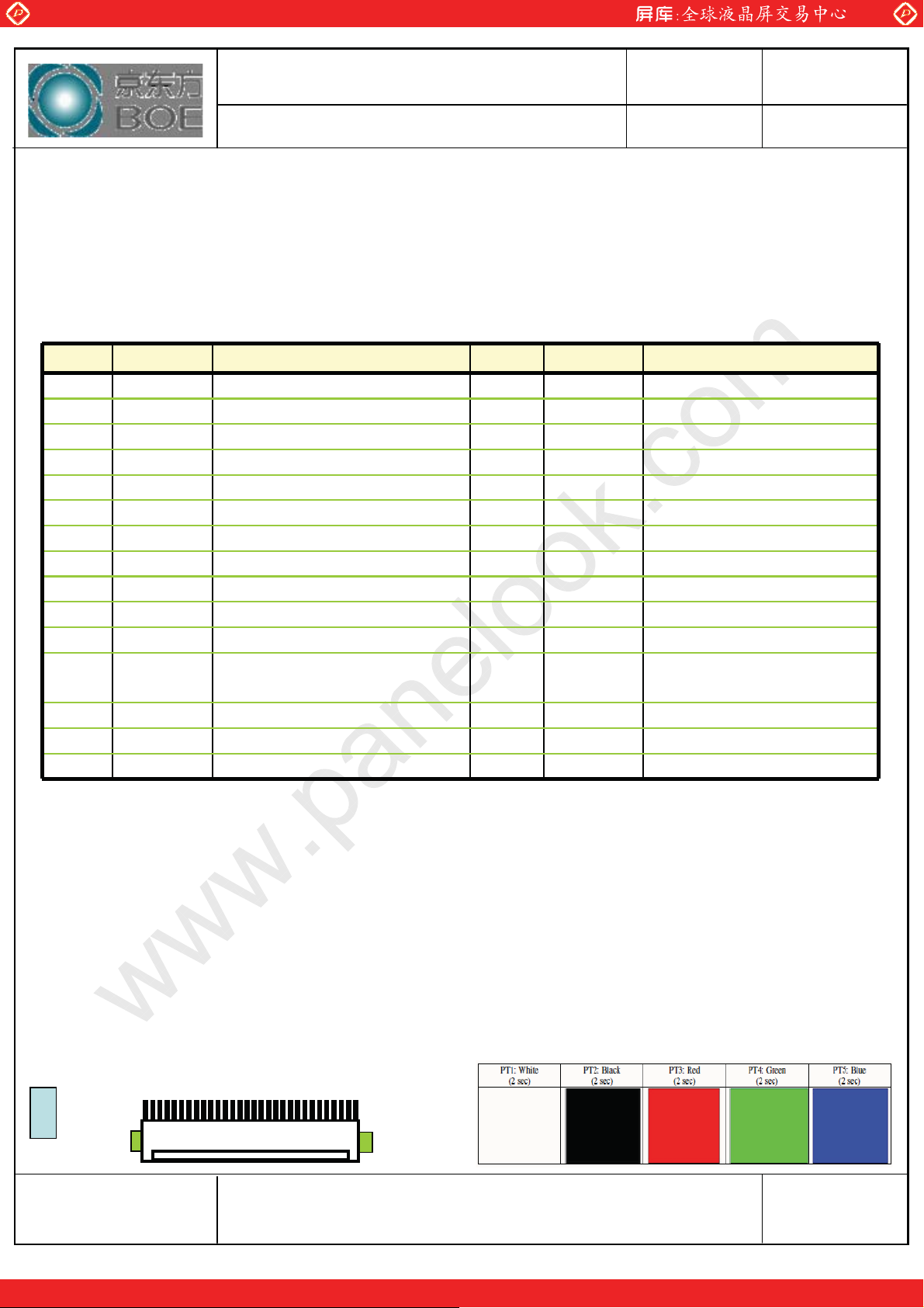
BIST Pattern
PAGE
8
OF 26
A4(210 X 297)
One step solution for LCD / PDP / OLED panel application: Datasheet, inventory and accessory!
www.panelook.com
 Loading...