

Page 1

TITLE:
PROPRIETARY NOTE
THIS SPECIFICATION IS THE PROPERTY OF BOE DT AND SHALL NOT BE
REPRODUCED OR COPIED WITHOUT THE WRITTEN PERMISSION OF BOE DT
AND MUST BE RETURNED TO BOE DT UPON ITS REQUEST
HV320WX2-506 Product Specification
BEIJING BOE DISPLAY TECHNOLOGY
SPEC. NUMBER
/S8-65-8A-073/P0
Bxxxx-xxxx-x(1/3)
PRODUCT GROUP
TFT LCD
REV.
P0
ISSUE DATE
2013.08.05
PAGE
of 24
1
A4(210 X 297)
A4(210 X 297)
Page 2
PRODUCT GROUP
REV ISSUE DATE
TFT LCD
P0 2013.08.05
REVISION HISTORY
REV. ECN NO. DESCRIPTION OF CHANGES DATE PREPARED
P0 - Initial Release 2013.08.05 Cuixiaopeng
SPEC. NUMBER
/S8-65-8A-073/P0
Bxxxx-xxxx-x(2/3)
SPEC. TITLE
HV320WX2-506 Product Specification
PAGE
of 24
2
A4(210 X 297)
Page 3
PRODUCT GROUP
REV ISSUE DATE
TFT LCD
P0 2013.08.05
Contents
No ITEM Page
REVISIONS HISTORY 2
CONTENTS
1 GENERAL DESCRIPTION
1.1 Introduction
1.2 Features
1.3 Applications
1.4 General Specification
2 ABSOLUTE MAXIMUM RATINGS 6
3 ELECTRICAL SPECIFICATIONS 7
3.1 TFT LCD Open Cell
4 INTERFACE CONNECTION 8
3
4
4.1 Open Cell Input Signal & Power
5 SIGNAL TIMING SPECIFICATIONS
5.1 Timing Parameters(DE Only Model)
5.2 Signal Timing Waveform
5.3 Power Sequence
6 OPTICAL SPECIFICATIONS 14
7 MECHANICAL CHARACTERISTICS 16
8 RELIABILITY TEST CONDITION 17
9 PRODUCT SERIAL NUMBER 18
10 PACKING INFORMATION
11 HANDING & CAUTIONS 21
12 APPENDIX
10
19
22
SPEC. NUMBER
/S8-65-8A-073/P0
Bxxxx-xxxxx-x (3/3)
SPEC. TITLE
HV320WX2-506 Product Specification
PAGE
of 24
3
A4(210 X 297)
Page 4
PRODUCT GROUP
REV ISSUE DATE
TFT LCD
P0 2013.08.05
1.0 GENERAL DESCRIPTION
1.1 Introduction
HV320WX2-506 is a color active matrix TFT LCD open cell using amorphous silicon TFT's
(Thin Film Transistors) as an active switching devices. This open cell has a 31.51 inch
diagonally measured active area with WXGA resolutions (1366 horizontal by 768 vertical
pixel array). Each pixel is divided into RED, GREEN, BLUE dots which are arranged in
vertical stripe and this open cell can display 16.7M colors. The TFT-LCD panel used for
this open cell is adapted for a low reflection and higher color type.
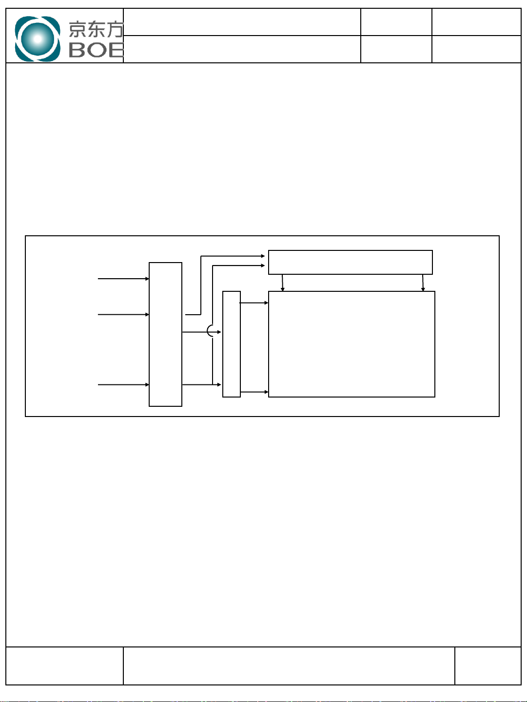
RGB(Mini-LVDS)
Source Driver Circuit
VDD
+12.0V
Mini-LVDS
Gate Driver Circuit
CN1
S1 S1366
G1
TFT - LCD Panel
(1366 × RGB × 768 pixels)
Power Supply
(60pin)
G768
1.2 Features
High-speed response
Low color shift image quality
8-bit color depth, display 16.7M colors
High luminance and contrast ratio, low reflection and wide viewing angle
AFFS technology is applied for high display quality
RoHS compliant
SPEC. NUMBER
/S8-65-8A-073/P0
Bxxxx-xxxxx-x (3/3)
SPEC. TITLE
HV320WX2-506 Product Specification
PAGE
of 24
4
A4(210 X 297)
Page 5
PRODUCT GROUP
REV ISSUE DATE
TFT LCD
P0 2013.08.05
1.3 Application
Home Alone Multimedia TFT-LCD TV
Display Terminals for Control System
High Definition TV(HD TV)
AV application Products
1.4 General Specification
< Table 1. General Specifications >
Parameter Specification Unit Remark
Glass thickness 0.5 mm 0.5t Glass
Active area
Number of pixels
Pixel pitch
Pixel arrangement Pixels RGB Vertical stripe
Display colors 16.7M(8bits-true) colors
Display mode Transmission mode, Normally Black
Open Cell
Transmittance
Weight 895 (typ.) gram
Surface Treatment
697.685(H) × 392.256(V)
1366(H) × 768(V)
170.25(H) × RGB× 510.75(V) ㎛
6.5 (typ.) %
Haze 10%, 3H, Semi-glare or Anti-
glare treatment (Front Polarizer)
Clear (Bottom Polarizer)
mm
pixels
At center point
with BOE BLU
SPEC. NUMBER
/S8-65-8A-073/P0
Bxxxx-xxxxx-x (3/3)
SPEC. TITLE
HV320WX2-506 Product Specification
PAGE
of 24
5
A4(210 X 297)
Page 6
PRODUCT GROUP
REV ISSUE DATE
TFT LCD
P0 2013.08.05
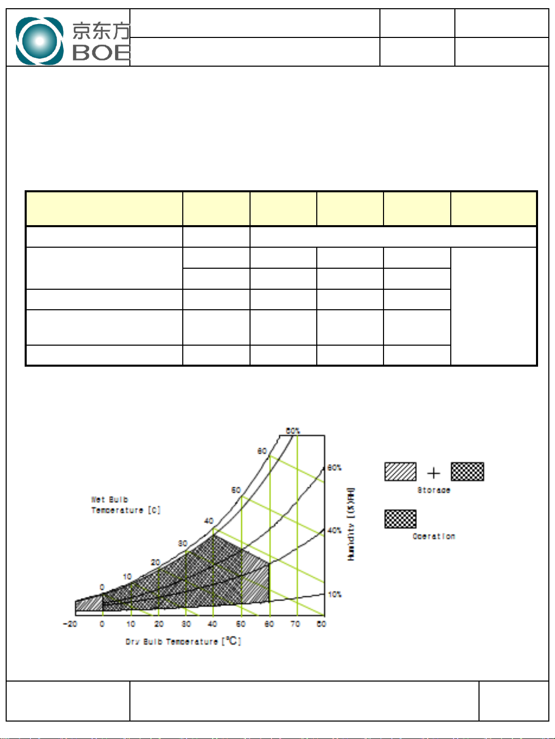
2.0 ABSOLUTE MAXIMUM RATINGS
The followings are maximum values which, if exceed, may cause faulty operation or
damage to the unit. The operational and non-operational maximum voltage and current
values are listed in Table 2.
< Table 2. Open Cell Electrical Specifications >
Parameter Symbol Min. Max. Unit Remark
Power Supply Voltage VDD To reference 3.0 ELECTRICAL SPECIFICATIONS
T
Operating Temperature
T
Storage Temperature T
Operating Ambient
Humidity
Hop 10 80 %RH
OP
SUR
ST
0 +50
0 +60
-20 +60
℃
℃
℃
[VSS=GND=0V]
Note 1
Storage Humidity Hst 10 80 %RH
Note 1 : Temperature and relative humidity range are shown in the figure below.
Wet bulb temperature should be 39 ℃ max. and no condensation of water.
SPEC. NUMBER
/S8-65-8A-073/P0
Bxxxx-xxxxx-x (3/3)
SPEC. TITLE
HV320WX2-506 Product Specification
PAGE
of 24
6
A4(210 X 297)
Page 7
PRODUCT GROUP
REV ISSUE DATE
TFT LCD
3.0 ELECTRICAL SPECIFICATIONS
3.1 TFT LCD Open Cell
< Table 3. Open Cell Electrical Specifications >
Characteristics Symbol Min Typ Max Unit
DC Supply Voltage
DC Supply Voltage
DC Supply Voltage
DC Supply Voltage
DC Supply Voltage
DC Supply Voltage
DC Supply Voltage
Von(与行频相同)
OE2
VDDD
Voff
Von
VREF 15.7 16 16.3
VCOM
VMID
AVDD
P0 2013.08.05
[Ta =25± 2 ℃]
3.0 3.3 3.6 V
-8.5 -8 -7.5 V
24 V
V
7.2 7.5 7.8 V
7.7 7.9 8.1 V
16 16.3 16.6 V
26.1V
Characteristics Symbol Min Typ Max Unit
DC Supply Voltage
DC Supply Voltage
DC Supply Voltage
DC Supply Voltage
DC Supply Voltage
DC Supply Voltage
DC Supply Voltage
Note: Vcom short-circuit current 400mA
Max Noise
Characteristics Symbol Max Unit
DC Supply Voltage
DC Supply Voltage
DC Supply Voltage
DC Supply Voltage
DC Supply Voltage
DC Supply Voltage
DC Supply Voltage
DVDD
Voff
Von
VREF
VCOM
VMID
AVDD
DVDD
Voff
Von
VREF
VCOM
VMID
AVDD
17.3V
50 100 mA
10 100 mA
20 100 mA
30 100 μA
50 200 mA
50 100 mA
250 350 mA
10 mV
25 mV
100 mV
30 mV
10 mV
100 mV
30 mV
SPEC. NUMBER
/S8-65-8A-073/P0
Bxxxx-xxxxx-x (3/3)
SPEC. TITLE
HV320WX2-506 Product Specification
PAGE
of 24
7
A4(210 X 297)
Page 8
PRODUCT GROUP
NO.
BOE PINMAP
Description
1
CPV
Gate driver clock input
2
NC
NC
3
STV
Gate driver vertical start pulse
4
OE1
Gate driver output enable signal
5
XAO
When XAO_L/R goes low, all outputs are fixed to VGG。
XAO_L/R signal has priority over OE_L/R
6
NC
NC
7
GND
GND
8,9
DVDD
Power supply for digital circuit.
10
GND
GND
11
VOFF
Negative power supply for gate
12
GND
GND
13,14
VON
Positive power supply for gate
15
GREF
Power supply for GAMMA reference
16,17
VCOM
common electrode for LCD
18
NC
NC
19
TP
Source driver latch signal
20
POL
Source driver polarity inversion signal
21
PAIRMODE
Selects mini-LVDS input mode: H:6-Pair Mode. (default) L:3-Pair Mode.
22
VMID
Power supply for analog circuit VMID=1/2AVDD
23
VMID
Power supply for analog circuit VMID=1/2AVDD
24~26
AVDD
Power supply for analog circuit
27
GND
GND
28~41
NC
NC
42
GND
GND
43
GND
GND
44
mLV5N
Differential inputs (mini-LVDS) for 8-bit RGB data and control signal
45
mLV5P
Differential inputs (mini-LVDS) for 8-bit RGB data and control signal
46
mLV4N
Differential inputs (mini-LVDS) for 8-bit RGB data and control signal
47
mLV4P
Differential inputs (mini-LVDS) for 8-bit RGB data and control signal
48
mLV3N
Differential inputs (mini-LVDS) for 8-bit RGB data and control signal
49
mLV3P
Differential inputs (mini-LVDS) for 8-bit RGB data and control signal
50
GND
GND
51
mLVCLKN
Differential inputs (mini-LVDS) for 8-bit RGB data and control signal
52
mLVCLKP
Differential inputs (mini-LVDS) for 8-bit RGB data and control signal
53
GND
GND
54
mLV2N
Differential inputs (mini-LVDS) for 8-bit RGB data and control signal
55
mLV2P
Differential inputs (mini-LVDS) for 8-bit RGB data and control signal
56
mLV1N
Differential inputs (mini-LVDS) for 8-bit RGB data and control signal
57
mLV1P
Differential inputs (mini-LVDS) for 8-bit RGB data and control signal
58
mLV0N
Differential inputs (mini-LVDS) for 8-bit RGB data and control signal
59
mLV0P
Differential inputs (mini-LVDS) for 8-bit RGB data and control signal
60
GND
GND
REV ISSUE DATE
TFT LCD
4.0 INTERFACE CONNECTION
4.1 Open Cell Input Signal & Power
4.1.1 Connector
P0 2013.08.05
SPEC. NUMBER
/S8-65-8A-073/P0
Bxxxx-xxxxx-x (3/3)
SPEC. TITLE
HV320WX2-506 Product Specification
PAGE
of 24
8
A4(210 X 297)
Page 9

PRODUCT GROUP
REV ISSUE DATE
TFT LCD
P0 2013.08.05
SPEC. NUMBER
/S8-65-8A-073/P0
Bxxxx-xxxxx-x (3/3)
SPEC. TITLE
HV320WX2-506 Product Specification
PAGE
of 24
9
A4(210 X 297)
Page 10

PRODUCT GROUP
REV ISSUE DATE
TFT LCD
5.0 SIGNAL TIMING SPECIFICATION
5.1 Timing Parameters (DE only mode)
< Table 7. Timing Table >
ITEM Symbol Min Typ Max Unit Note
Period t
CLK
Frequency - 56 75.4 85.0 MHz
Period t
Hsync
Frequency f
Period t
Vsync
Frequency f
CLK
HP
H
VP
V
P0 2013.08.05
11.8 13.3 17.9 ns
1450 1560 2000 t
CLK
39.4 48.4 55 KHz
778 806 1200 t
HP
47 60 65 Hz
Horizontal
Valid t
HV
- 1366 - t
CLK
Active
Display Term
Vertical Active
Display Term
Notes: This product is DE only mode. The input of Hsync & Vsync signal does not have an effect on normal
operation.
Total t
Valid t
Total t
HP
VV
VP
1450 1560 2000 t
- 768 - t
778 806 1200 t
CLK
HP
HP
SPEC. NUMBER
/S8-65-8A-073/P0
Bxxxx-xxxxx-x (3/3)
SPEC. TITLE
HV320WX2-506 Product Specification
PAGE
of 24
10
A4(210 X 297)
Page 11

PRODUCT GROUP
REV ISSUE DATE
5.2 Signal Timing Waveform
TFT LCD
P0 2013.08.05
SPEC. NUMBER
/S8-65-8A-073/P0
Bxxxx-xxxxx-x (3/3)
SPEC. TITLE
HV320WX2-506 Product Specification
PAGE
of 24
11
A4(210 X 297)
Page 12

PRODUCT GROUP
REV ISSUE DATE
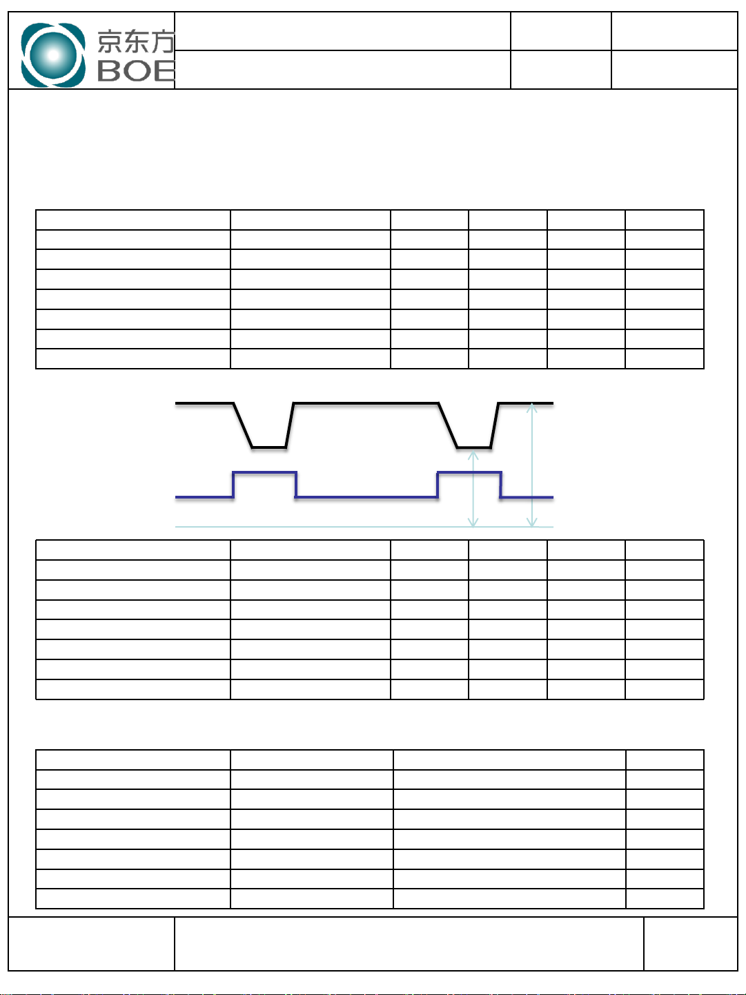
5.3 Power Sequence
POWER ON
XAO
DVDD
AVDD
10%
T1
90%
T2
TFT LCD
Power sequence
P0 2013.08.05
10%
T9
20%
GREF
VMID
VOFF
VON
VCOM
DATA
T3
T4
T5
T6
T7
T8
SPEC. NUMBER
/S8-65-8A-073/P0
Bxxxx-xxxxx-x (3/3)
SPEC. TITLE
HV320WX2-506 Product Specification
PAGE
of 24
12
A4(210 X 297)
Page 13

PRODUCT GROUP
T
Min
Type
Max
Unit
Note
T1
0
10
ms
T2
0
ms
T3
0
ms
AVDD must be higher than VMID and
GREF all the time
T4
0
ms
AVDD must be higher than VMID and
GREF all the time
T5
0
ms
T6
0
ms
T7
0
ms
T8
0
ms
T9
0
ms
REV ISSUE DATE
TFT LCD
P0 2013.08.05
SPEC. NUMBER
/S8-65-8A-073/P0
Bxxxx-xxxxx-x (3/3)
SPEC. TITLE
HV320WX2-506 Product Specification
PAGE
of 24
13
A4(210 X 297)
Page 14

PRODUCT GROUP
REV ISSUE DATE
TFT LCD
P0 2013.08.05
6.0 OPTICAL SPECIFICATIONS
The test of optical specifications shall be measured in a dark room (ambient luminance1 lux
and temperature=252℃) with the equipment of Luminance meter system (Goniometer
system and PR730) and test unit shall be located at an approximate distance 50cm from the
LCD surface at a viewing angle of θ and Φ equal to 0. We refer to θ
o’clock direction (the “right”), θ
) as the 9 o’clock direction (“left”) and θ
(= θ12) as the 12 o’clock direction (“upward”), θ
Ø=90
(= θ6 ) as the 6 o’clock direction (“bottom”). While
Ø=270
scanning θ and/or Ø, the center of the measuring spot on the Display surface shall stay
fixed. The measurement shall be executed after 30 minutes warm-up period. VDD shall be
12.0V +/-10% at 25C. Optimum viewing angle direction is 6 ’clock.
< Table 10. Optical Table >
[VDD = 12.0V, Frame rate = 60Hz, Ta =25± 2 ℃]
Parameter Symbol Condition Min Typ Max Unit Remark
Viewing
Horizontal
Angle
Vertical
Contrast ratio CR
Θ
Θ
Θ
Θ
12
3
9
6
CR > 10
900:1 1200:1 - Note 2
89 Deg.
89 Deg.
89 Deg.
89 Deg.
Ø=0
(=θ
3
) as the 3
Ø=180
Note 1
(= θ
9
White
W
W
Red
Reproduction
of color
R
G
Green
G
Blue
Response Time G to G T
R
B
B
x
y
x
y
x
y
Θ = 0
(Center)
Normal
Viewing
TYP.
- 0.03
Angle
x
y
g
With BOE
Module
- 8 10 ms Note 4
0.280
0.290
-
-
-
-
-
-
TYP.
+ 0.03
Gamma Scale 2.0 2.2 2.4
Luminance of Black Y
b
- - 0.5 cd/m
Cell Transmittance 6.5 % Note 5
SPEC. NUMBER
/S8-65-8A-073/P0
SPEC. TITLE
HV320WX2-506 Product Specification
2
Note 3
Note 6
PAGE
of 24
14
Bxxxx-xxxxx-x (3/3)
A4(210 X 297)
Page 15

PRODUCT GROUP
REV ISSUE DATE
TFT LCD
P0 2013.08.05
Note :
1. Viewing angle is the angle at which the contrast ratio is greater than 10. The viewing are
determined for the horizontal or 3, 9 o’clock direction and the vertical or 6, 12 o’clock
direction with respect to the optical axis which is normal to the LCD surface.
2. Contrast measurements shall be made at viewing angle of = 0 and at the center of the LCD
surface. Luminance shall be measured with all pixels in the view field set first to white, then
to the dark (black) state. (See Figure 1 shown in Appendix) Luminance Contrast Ratio (CR)
is defined mathematically.
CR =
3. The color chromaticity coordinates specified in Table 9.shall be calculated from the spectral
data measured with all pixels first in red, green, blue and white. Measurements shall be
made at the center of the panel.
4. Response time Tg is the average time required for display transition by switching the input
signal as below table and is based on Frame rate fV =60Hz to optimize.
Each time in below table is defined as Figure 2and shall be measured by switching the input
signal for “any level of gray(bright)”and “any level of gray(dark)”.
Luminance when displaying a white raster
Luminance when displaying a black raster
5. Definition of Transmittance (T%) :
Module is with white(L255) signal input
Transmittance =
6. There will be less than 3 times of black luminance difference between center and each 4
corners. The position of 4 corners are described in Appendix Figure.4
SPEC. NUMBER
/S8-65-8A-073/P0
Bxxxx-xxxxx-x (3/3)
Luminance of LCD Module
Luminance of BLU
SPEC. TITLE
HV320WX2-506 Product Specification
× 100 %
PAGE
of 24
15
A4(210 X 297)
Page 16

PRODUCT GROUP
REV ISSUE DATE
TFT LCD
P0 2013.08.05
7.0 MECHANICAL CHARACTERISTICS
7.1 Dimensional Requirements
Figure 3 (located in Appendix) shows mechanical outlines for the model HV320WX2-261.
Other parameters are shown in Table 10.
< Table 11. Dimensional Parameters >
Parameter Specification Unit
Glass thickness 0.5 mm
Active area
Pixel pitch
Number of pixels
Weight 895 (typ.) gram
1366(H) × 768(V) (1 pixel = R + G + B dots)
697.685 (H) × 392.256(V)
0.51(H) × 0.51(V)
mm
mm
pixels
7.2 Semi-Glare and Polarizer Hardness
The surface of the LCD has an semi-glare coating to minimize reflection and a coating to
reduce scratching.
SPEC. NUMBER
/S8-65-8A-073/P0
SPEC. TITLE
HV320WX2-506 Product Specification
PAGE
16
of 24
Bxxxx-xxxxx-x (3/3)
A4(210 X 297)
Page 17

PRODUCT GROUP
REV ISSUE DATE
8.0 Reliability Test Condition
< Table 12. Reliability Test Condition >
Item Test Condition
High Temperature Storage Test
Low Temperature Storage Test
High Temperature & High Humidity
Operation Test
TFT LCD
Ta = 60 ℃, 240 hrs
Ta = -20 ℃, 240 hrs
Ta = 50 ℃, 80%RH, 240hrs
P0 2013.08.05
High Temperature Operation Test
Low Temperature Operation Test
Ta = 50 ℃, 240hrs
Ta = 0 ℃, 240hrs
SPEC. NUMBER
/S8-65-8A-073/P0
Bxxxx-xxxxx-x (3/3)
SPEC. TITLE
HV320WX2-506 Product Specification
PAGE
of 24
17
A4(210 X 297)
Page 18

PRODUCT GROUP
REV ISSUE DATE
TFT LCD
9.0 PRODUCT SERIAL NUMBER
HV320WX2-506
P0 2013.08.05
1 2 3 4 5 6 7
X X X X X X X X X X X X X X X X X
1. Control Number
2. Rank / Grade
3. Line Classification
4. Year (2011 : 11, 2012 : 12, …)
SPEC. NUMBER
/S8-65-8A-073/P0
SPEC. TITLE
HV320WX2-506 Product Specification
5. Month (1,2,3, … , 9, X, Y, Z)
6. Internal Use
7. Serial Number
PAGE
18
of 24
Bxxxx-xxxxx-x (3/3)
A4(210 X 297)
Page 19

PRODUCT GROUP
REV ISSUE DATE
TFT LCD
P0 2013.08.05
10.0 PACKING INFORMATION
BOE provides the standard shipping container for customers, unless customer specifies
their packing information. The standard packing method and Barcode information are
shown in below. The packing material ESD Spec is shown in Appendix Figure 7.
10.1 Packing Order
Dense box
up down
240pcs Open Cell / Pallet
15pcs Open Cell / Dense box
SPEC. NUMBER
/S8-65-8A-073/P0
Bxxxx-xxxxx-x (3/3)
SPEC. TITLE
HV320WX2-506 Product Specification
PAGE
of 24
19
A4(210 X 297)
Page 20

PRODUCT GROUP
REV ISSUE DATE
TFT LCD
10.2 Packing Note
Box Dimension : 880mmL× 605mmW× 140mmH
Package Quantity in one Box : 15pcs
10.3 Box Label
Label Size : 110 mm (L) 55 mm (W)
Contents
Model : HV320WX2-506
Q`ty : 15 Open Cell in one box.
Serial No. : Box Serial No. See next page for detail description.
Date : Packing Date
FG Code : FG Code of Product
P0 2013.08.05
00 0 00 0 0 000000
Type Grade Year Month ITEM-CODE Serial_no
SPEC. NUMBER
/S8-65-8A-073/P0
HV320WX2-506
0000000000000
XXXX
SPEC. TITLE
HV320WX2-506 Product Specification
15
201X.X.XX
Internal CODE
RoHS Mark
PAGE
20
of 24
Bxxxx-xxxxx-x (3/3)
A4(210 X 297)
Page 21

PRODUCT GROUP
REV ISSUE DATE
TFT LCD
P0 2013.08.05
11.0 HANDLING & CAUTIONS
CAUTIONS
(1) Cautions when taking out the Panel
Pick the pouch only, when taking out panel from a shipping package.
(2) Cautions for handling the panel
As the electrostatic discharges may break the LCD Panel, handle the LCD panel with
care. Peel a protection sheet off from the LCD panel surface as slowly as possible.
As the LCD panel and back -light element are made from fragile glass material, impulse
and pressure to the LCD panel should be avoided.
As the surface of the polarizer is very soft and easily scratched, use a soft dry cloth
without chemicals for cleaning.
Do not pull the interface connector in or out while the LCD panel is operating.
Put the panel display side down on a flat horizontal plane.
Handle connectors and cables with care.
(3) Cautions for the operation
When the panel is operating, do not lose CLK, ENAB signals. If any one of these
signals Is lost, the LCD panel would be damaged.
Obey the supply voltage sequence. If wrong sequence is applied, the panel would be
damaged.
(4) Cautions for the atmosphere
Dew drop atmosphere should be avoided.
Do not store and/or operate the LCD panel in a high temperature and/or humidity
atmosphere. Storage in an electro-conductive polymer packing pouch and under
relatively low temperature atmosphere is recommended.
(5) Cautions for the panel characteristics
Do not apply fixed pattern data signal to the LCD panel at product aging.
Applying fixed pattern for a long time may cause image sticking.
(6) Other cautions
Do not disassemble and/or re-assemble LCD panel.
Do not re-adjust variable resistor or switch etc.
When returning the panel for repair or etc., Please pack the panel not to be broken. We
recommend to use the original shipping packages.
SPEC. NUMBER
/S8-65-8A-073/P0
Bxxxx-xxxxx-x (3/3)
SPEC. TITLE
HV320WX2-506 Product Specification
PAGE
of 24
21
A4(210 X 297)
Page 22

PRODUCT GROUP
(L = 5 0c m )
REV ISSUE DATE
12.0 APPENDIX
TFT LCD
< Figure 1. Measurement Set Up >
P0 2013.08.05
PR730
< Figure 2. Response Time Testing >
SPEC. NUMBER
/S8-65-8A-073/P0
Bxxxx-xxxxx-x (3/3)
SPEC. TITLE
HV320WX2-506 Product Specification
PAGE
of 24
22
A4(210 X 297)
Page 23

PRODUCT GROUP
REV ISSUE DATE
1/10V
TFT LCD
< Figure 4. Optical Measurement Locations >
1/10H 1/2H 9/10H
P0 2013.08.05
1/2V
9/10V
Test points
Active Area: 697.7 × 392.3mm
SPEC. NUMBER
/S8-65-8A-073/P0
Bxxxx-xxxxx-x (3/3)
SPEC. TITLE
HV320WX2-506 Product Specification
PAGE
of 24
23
A4(210 X 297)
Page 24

PRODUCT GROUP
避让区域
避让区域
REV ISSUE DATE
TFT LCD
P0 2013.08.05
< Figure 3. Open Cell Outline Dimensions (Front View) >
SPEC. NUMBER
/S8-65-8A-073/P0
Bxxxx-xxxxx-x (3/3)
SPEC. TITLE
HV320WX2-506 Product Specification
PAGE
of 24
24
A4(210 X 297)
 Loading...