

Page 1
www.armdesigner.com
Idea6410
Single Board Computer
Hardware Reference Guide
IDEA6410 Hardware Reference Guide
1
Page 2

www.armdesigner.com
IDEA6410 Hardware Reference Guide
2
1. Introduction
1.1. About this Manual
This manual is intended to provide the user with an overview of the board and benefits,
complete features specifications, and set up procedures. It contains important safety
information as well.
1.2. Feedback and Update to this Manual
To help our customers make the most of our products, we are continually making
additional and updated resources available on the Boardcon website
(
www.armdesigner.com).
These include manuals, application notes, programming examples, and updated software
and hardware. Check in periodically to see what’s new!
When we are prioritizing work on these updated resources, feedback from customers is
the number one influence, If you have questions, comments, or concerns about your
product or project, please no hesitate to contact us at
1.3. Limited Warranty
Boardcon warrants this product to be free of defects in material and workmanship for a
period of one year from date of buy. During this warranty period Boardcon will repair or
replace the defective unit in accordance with the following process:
A copy of the original invoice must be included when returning the defective unit to
Boardcon. This limited warranty does not cover damages resulting from lighting or other
power surges, misuse, abuse, abnormal conditions of operation, or attempts to alter or
modify the function of the product.
This warranty is limited to the repair or replacement of the defective unit .In no event shall
Boardcon be liable or responsible for any loss or damages, including but not limited to any
lost profits, incidental or consequential damages, loss of business, or anticipatory profits
arising from the use or inability to use this products.
Repairs make after the expiration of the warranty period are subject to a repair charge and
the cost of return shipping. Please contact Boardcon to arrange for any repair service and
to obtain repair charge information.
Page 3

www.armdesigner.com
IDEA6410 Hardware Reference Guide
3
1. OVERVIEW........................................................................................................................................4
1.1. HIGHLIGHTS ...................................................................................................................................4
1.2. IDEA6410 BLOCK DIAGRAM.........................................................................................................6
2. IDEA6410 POWER DESIGN...........................................................................................................7
2.1. POWER SUPPLY FOR IDEA6410......................................................................................................7
2.1.1. Power Supply ways............................................................................................................7
2.1.2 The Schematic drawing of power input............................................................................7
2.1.3. Voltage value on circuit dot...............................................................................................8
2.2. POWER ELECTRICAL CHARACTERISTICS AND POWER TIME SEQUENCE OF S3C6410........................9
2.3. IDEA6410 POWER SUPPLY BLOCK DIAGRAM...............................................................................11
2.4. BOOTLOADER STARTUP CONFIGURATION MODE............................................................................12
3. IDEA6410 HARDWARE DESIGN AND INTERFACES DESCRIPTION................................14
3.1. NAND FLASH................................................................................................................................14
3.2. DDR RAM...................................................................................................................................15
3.3. NOR FLASH ..................................................................................................................................15
3.4. SERIAL INTERFACE .......................................................................................................................16
4. INTERFACE.....................................................................................................................................19
4.1. USB HOST....................................................................................................................................19
4.2. USB OTG....................................................................................................................................20
4.3. JTAG............................................................................................................................................20
4.4. SD CARD......................................................................................................................................22
4.5. CAMERA INTERFACES ...................................................................................................................22
4.6. TFT LCD AND TOUCH SCREEN INTERFACE..................................................................................24
4.7. RESET KEY ...................................................................................................................................26
4.8. AUDIO INTERFACE ........................................................................................................................28
4.9. BUZZER........................................................................................................................................29
4.10. 100M ETHERNET INTERFACE......................................................................................................31
4.12. TVOUT INTERFACE....................................................................................................................33
4.11. HIGH SPEED SPI, MMC2 AND I2C INTERFACE ...........................................................................33
4.12. USER BUTTONS AND LEDS.........................................................................................................34
4.13. GPIO AND ADC.........................................................................................................................35
4.14. RTC ...........................................................................................................................................37
4.15. 8X8 MATRIX KEYBOARD ............................................................................................................38
5. OPTIONAL MODULES..................................................................................................................40
5.1. WIFI MODULE .............................................................................................................................40
5.2. GPS MODULE...............................................................................................................................40
5.3. CAMERA MODULE........................................................................................................................40
5.4. 7 INCH TFT LCD MODULE...........................................................................................................40
5.5. 4*4 MATRIX KEYBOARD AND USB_HUB MODULE.....................................................................41
Page 4

www.armdesigner.com
IDEA6410 Hardware Reference Guide
4
1. Overview
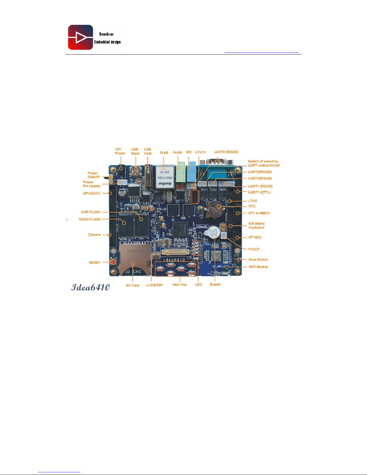
The Idea6410 is a compact full-featured Embedded Single Board Computer(SBC) based
upon Samsung ARM11 S3C6410, designed specifically for Mobile Internet Device ,
Notebook, handheld / 3G mobile implementations. Its functional contents are similar to the
latest generation of Pocket PC's and smartphones, This computer allows easy embedded
application development through PC-Compatible tools and methods, while ensuring
in-field reliability and ruggedness for end-user systems.Idea6410 run without fans or heat
sinks in the temperature range of -20° to +70°C. Other chip-level features include 4
UARTs, SPI, I2C, a real-time clock with a separate power domain, and NAND Flash and
DDR memory controllers. These features make the devices particularly suitable for
automotive and industrial control applications as well as medical systems. In addition to
Windows Embedded CE 6.0 and Linux2.6 support,ready-to-run Android and Ubuntu are
available from Boardcon.
1.1. Highlights
. Rugged Single Board Computer(120mmx58mm) achieved through modern SMD
technology
. Improved interference safety achieved through multi-layer PCB technology and
dedicated ground pins
. Controller signals and ports extend to connectors aligning two sides of the board
. Four Ready-to-Run software package: WinCE6.0, Linux2.6.24, Android and Ubuntu
. Working temperature: -20°C to 70°C
. Processor: Samsung S3C6410, ARM1176JZF-S, up to 667MHz.
. Power supply: +12V
. 128MB Mobile DDR SDRAM, 133MHz, 32bit, Samsung K4X51163PC
. 256MB NAND Flash, 8bit, Samsung K2F2G08
. 2M Bytes NOR Flash, AMD AM29LV160DB
. SDIO WIFI Module, supporting IEEE802.11b/g
. LCD/Touch Screen interface. Supporting 3.5 inch TFT LCD, 4.3 inch TFT LCD and 7
inch TFT LCD.
. Many modules are available for your choice- GPS, WIFI, Camera, USB HUB+4x4
Matrix Keyboard.
. 24 GPIO, ADC, SPI,IIC and MMC connectors
. One audio input interface (3.5mm audio jack)
. One 2-channel audio output interface (3.5mm audio jack)
. One 100M Ethernet interface (RJ45)
. One USB2.0 Device port (Mini USB type interface)
Page 5

www.armdesigner.com
IDEA6410 Hardware Reference Guide
5
. Four serial ports (Two are five-wire RS-232 DB9 interface, another two are three-wire
TTL serial port led out from a 20-pin expansion connector )
. SD/MMC interface (supports 3.3V and 1.8V logic voltage)
. Camera interface (10x2 pins header, supporting the mode of ITU-R 601/656 8bit)
. One 5x2 pins JTAG interface
. Seven buttons (Reset, Boot, User defined, On/Off)
. TVOUT
Page 6
www.armdesigner.com
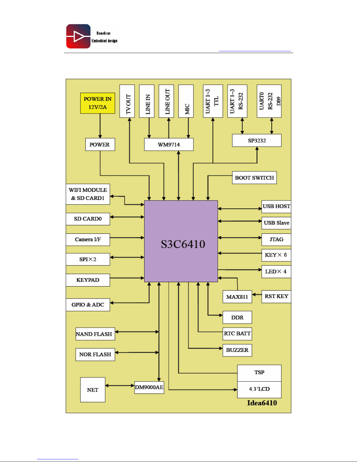
1.2. IDEA6410 Block Diagram
IDEA6410 Hardware Reference Guide
6
Page 7
www.armdesigner.com
2. IDEA6410 Power design
2.1. Power Supply for IDEA6410
2.1.1. Power Supply ways
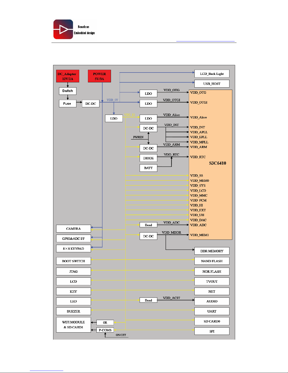
The IDEA6410 power design adopts distributed fabric, adopting absolute power chip to
power supply respective for S3C6410 and peripheral devices.
The main chip S3C6410 runs on frequency at 533MHz, the CPU board is supplying power
for CPU with 1.1V ARM Kernel power VDD_ARM, 1.3V PLL-VCC and startup power of the
chip internal logic power VDD_xPLL and VDD_INT ,1.2V startup power VDD_Alive, 1.8V
DDR memory VDD_MEM, 3.3V I/O and the other peripheral devices.
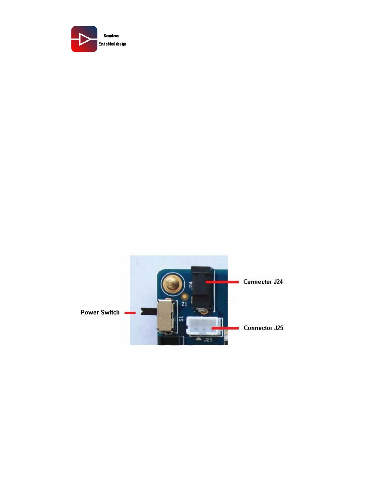
There are two ways for power supply for IDEA6410 Single Board Computer.
(1). Using Power Adapter through mini DC_IN connector J24 to send 12V/2A to the board
(2). Using Battery 5V/3A through connector J25 to power supply.
Below picture-2 shows the two connectors:
Picuture-2
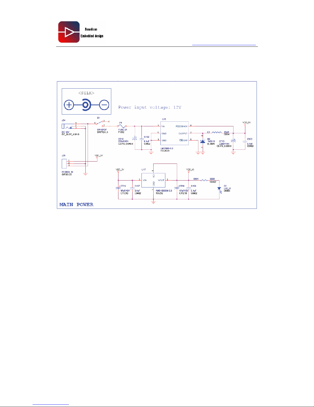
2.1.2 The Schematic drawing of power input
IDEA6410 Hardware Reference Guide
7
Page 8
www.armdesigner.com
Below picture-3 shows the schematic drawing.
Picture-3
2.1.3. Voltage value on circuit dot
. VDD_5V: 5V,
VDD_IO: 3.3V
VDD_OTG: 3.3V
VDD_OTGI: 1.2V
VDD_Alive: 1.2V
VDD_INT: 1.3V
VDD_ARM: 1.2V
VDD_RTC: 3V
VDD_ADC: 3.3V
VDD_MDDR: 1.8V
VDD_AC97:3.3V
VDD_WIFI: 3.3V
IDEA6410 Hardware Reference Guide
8
Page 9
www.armdesigner.com
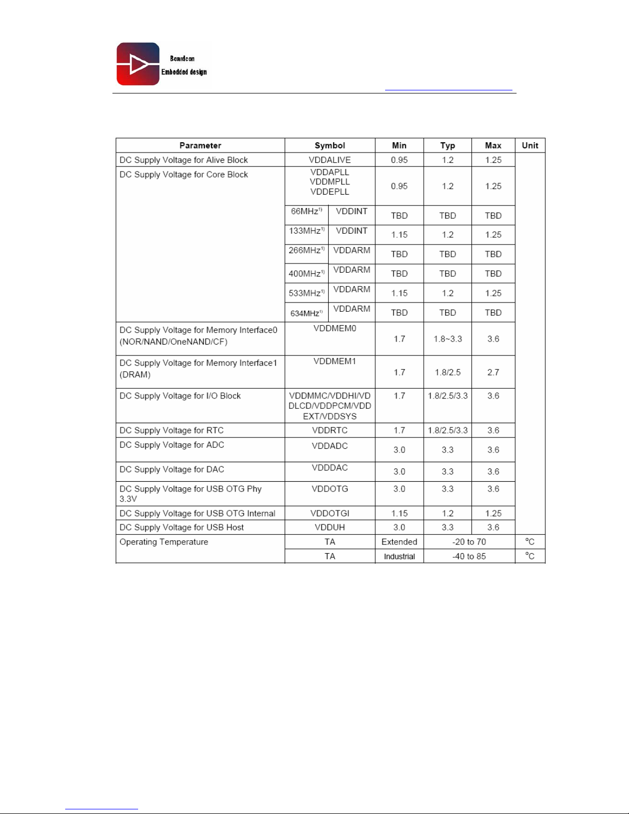
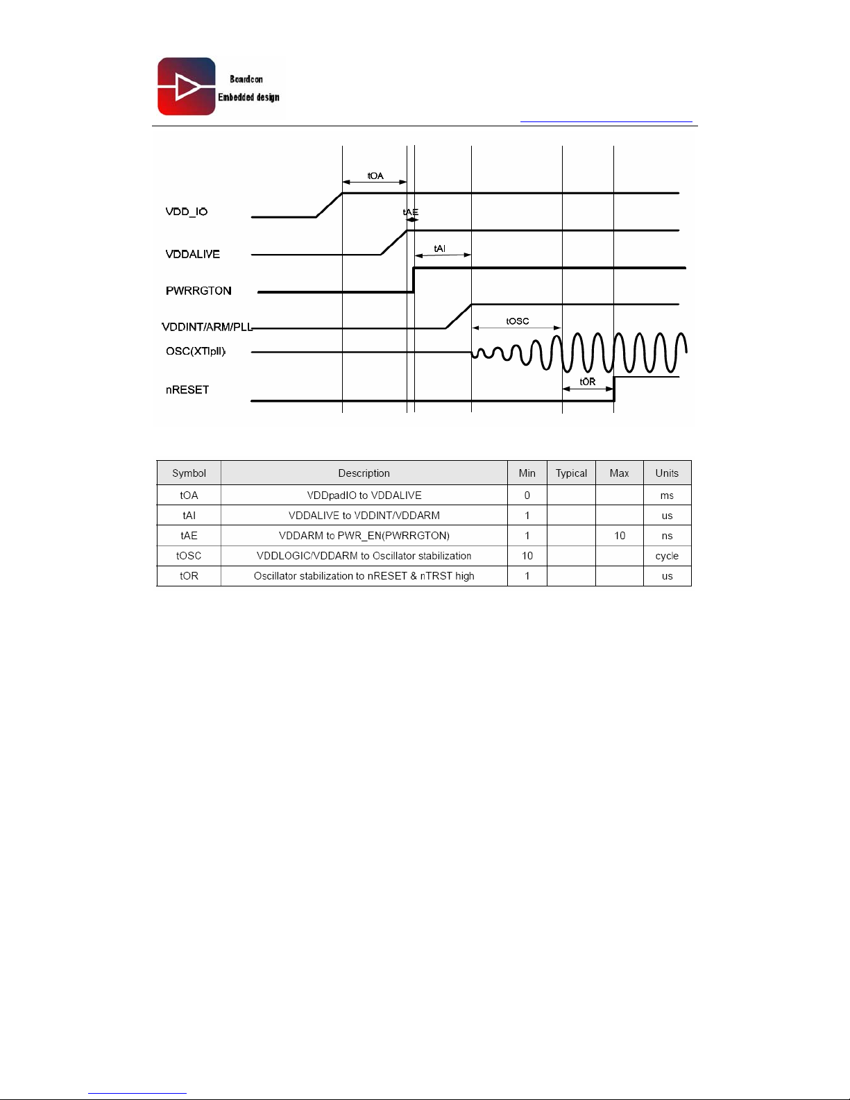
2.2. Power electrical characteristics and power time sequence of S3C6410
IDEA6410 Hardware Reference Guide
9
Page 10
www.armdesigner.com
IDEA6410 Hardware Reference Guide
10
Page 11
www.armdesigner.com
2.3. IDEA6410 Power Supply block diagram
IDEA6410 Hardware Reference Guide
11
Page 12
www.armdesigner.com
IDEA6410 Hardware Reference Guide
12
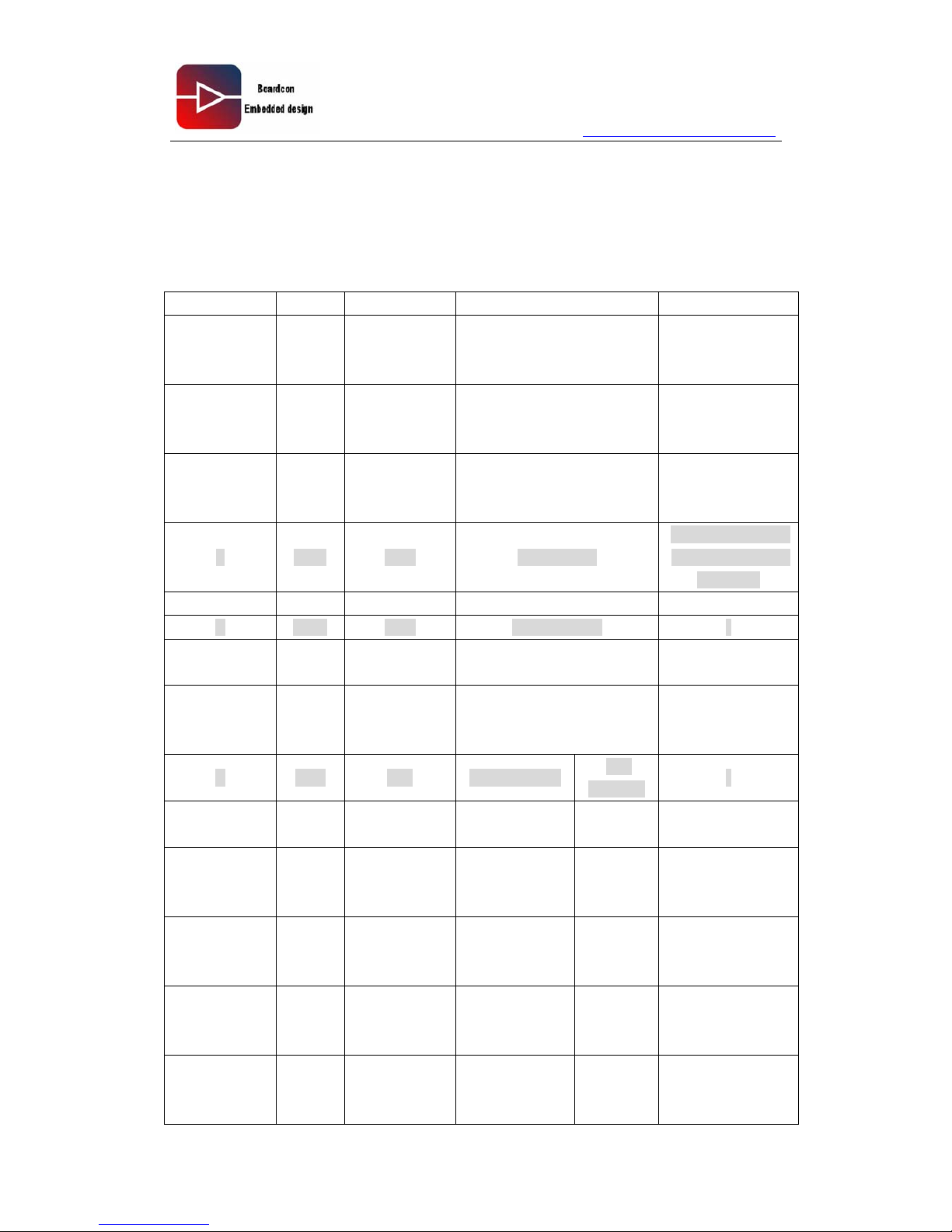
2.4.Bootloader startup configuration mode
The main chip S3C6410 supports many kinds of startup mode such as Nand Flash, Nor
Flash, OneNand and SD Card and so on. It selects startup device and mode through
configuring different pins' status when the system started. Below figure 2.5 shows the
startup mode of S3C6410.
XSELNAND ON[4:1] EINT[15:13] Boo-up Device Note
1 0000 XXX Nand Flash
512k page size,
addressing cycle
is 3 clock
1 0001 XXX Nand Flash
512k page size,
addressing cycle
is 4 clock
1 0010 XXX Nand Flash
2048k page size,
addressing cycle
is 4 clock
1 0011 XXX Nand Flash
2048k page size,
addressing cycle
is 5 clock
X 0100 XXX SROM(8bit) -
X 0101 XXX SROM(16bit) -
0 0110 XXX OneNand
Can not use Nand
Flash
X 0111 XXX Modem
SCn2 can not be
connected with
SROM
X 1111 000 Internal ROM
SD
access0
-
X 1111 001 Internal ROM OneNand -
1 1111 010 Internal ROM
Nand
Flash
512k page size,
addressing cycle
is 3 clock
1 1111 011 Internal ROM
Nand
Flash
512k page size,
addressing cycle
is 4 clock
1 1111 100 Internal ROM
Nand
Flash
2048k page size,
addressing cycle
is 4 clock
1 1111 101 Internal ROM
Nand
Flash
2048k page size,
addressing cycle
is 5 clock
Page 13
www.armdesigner.com
1 1111 110 Internal ROM
Nand
Flash
4096k page size,
addressing cycle
is 5 clock
X 1111 111 Internal ROM
SD
access1
-
Figure-2.5
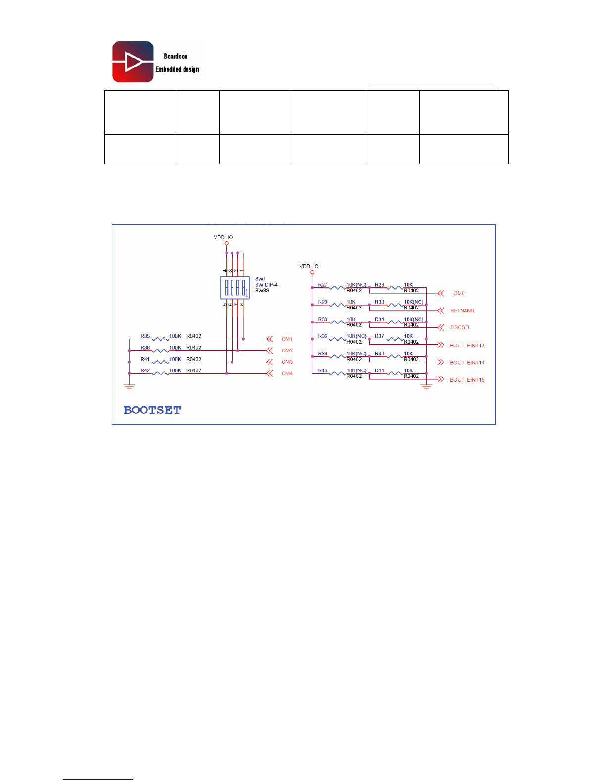
IDEA6410 Supports NOR Flash, Nand Flash, SD Card startup mode, please see the blue
part of above picture. Also the picture-2.6 is a part of IDEA6410 startup mode.
Picture-2.6
On above picture-2.6, “OM0” is chip S3C6410 clock source select signal. It selects
“XTIpll “ when “OM0” is “0”, it select “EXTCLK” when “OM0” is “1”. The IDEA6410 uses
“XTIpll”.
“SELNAND” is a signal of selecting memory type, it is high level when selects NAND Flash,
it is low level when selects ONENAND. IDEA6410 uses NAND Flash.
EINT13-EINT15 are device selected pins of IROM startup mode, when adopts IROM
startup mode, the main chip S3C6410 runs settled program in advance then reads
EINT15,EINT14,EINT13 three pins' status with different configuration to select startup
device, the detailed configuration please see figure-2.5.
It is IROM startup mode when user selected SD Card as startup device. At this mode,
EINT15, EINT14, EINT13 are low level. So the user will see on IDEA6410 ,there signals
EINT15,EINT14,EINT13 are directly connected ground.
DBGSEL is JTAG interface call select signal, about it detail, please see the chapter 4.3.
On IDEA6410 Single Board Computer, the three pins EINT13-15 had been set into low
level, please select startup mode by configuring OM1-OM4 and SELNAND, the switch
SW1 moves to subject place, please see below figure-2.5 of SW1 configuration.
IDEA6410 Hardware Reference Guide
13
Page 14
www.armdesigner.com
Ports OM1 OM2 OM3 OM4
SW1’s Position 1 2 3 4
Nor Flash boot-up 1 0 1 0
Nand Flash boot-up 1 1 0 0
SD boot-up 1 1 1 1
Figure-2.5
Note: a. “1” is SW1 ON, “0” is SW1 OFF, “X” is high level or low level.
b. The default startup mode of IDEA6410 is NAND Flash.
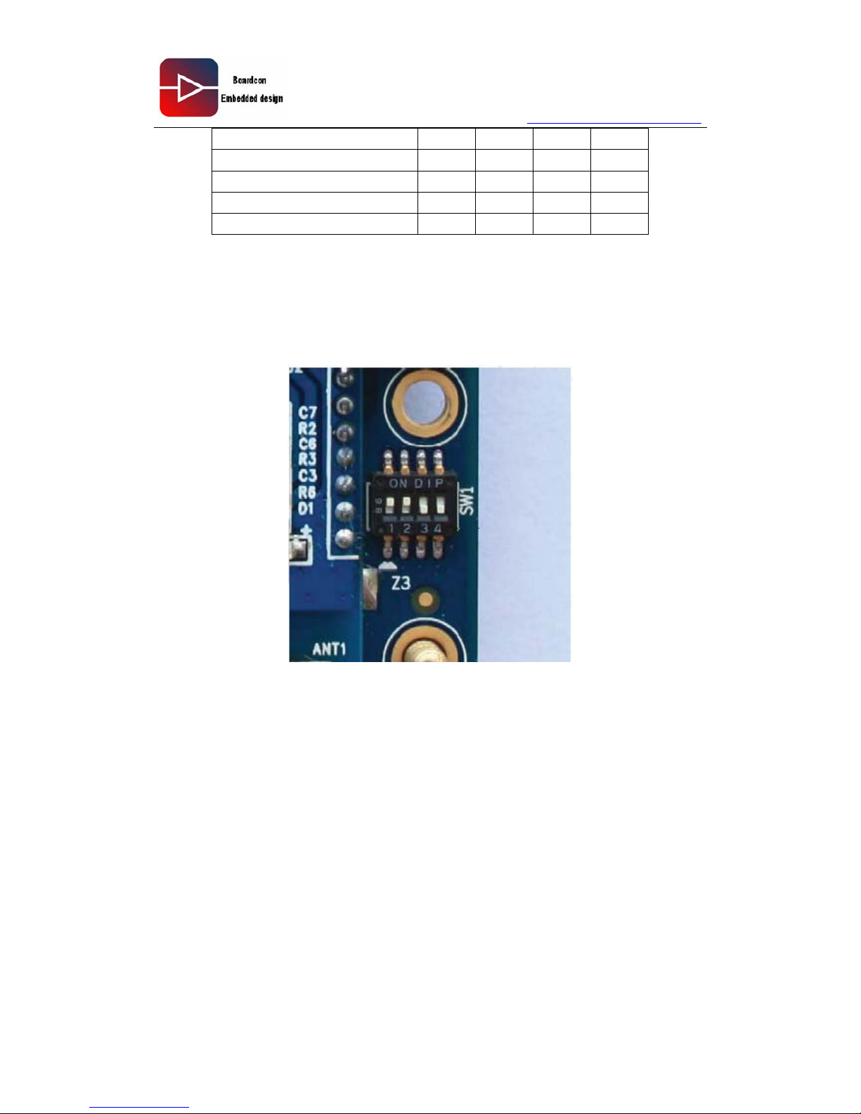
Below is a picture-2.7 about SW1.
Picture-2.7
OM0 is chip S3C6410 clock source select signal. It selects XTIpll when OM0 is “o”, it
select EXTCLK when OM0 is “1”. The IDEA6410 uses XTIpll.
3. IDEA6410 Hardware Design and interfaces description
3.1. Nand Flash
IDEA6410 Single Board Computer selected SLC Nand FLASH K9F2G08 from Samsung,
its size is 256M Bytes, mainly for storage Kernel, application, file system and user data.
Additionally, may parts that are footprint and functionally compatible with the Nand Flash
devices listed above may also be used with the IDEA6410.
As of the printing of this manual, these NAND Flash devices generally have a life
expectancy of at least 100,000 erase/program cycles and a data retention rate of 10
IDEA6410 Hardware Reference Guide
14
Page 15
www.armdesigner.com
years.
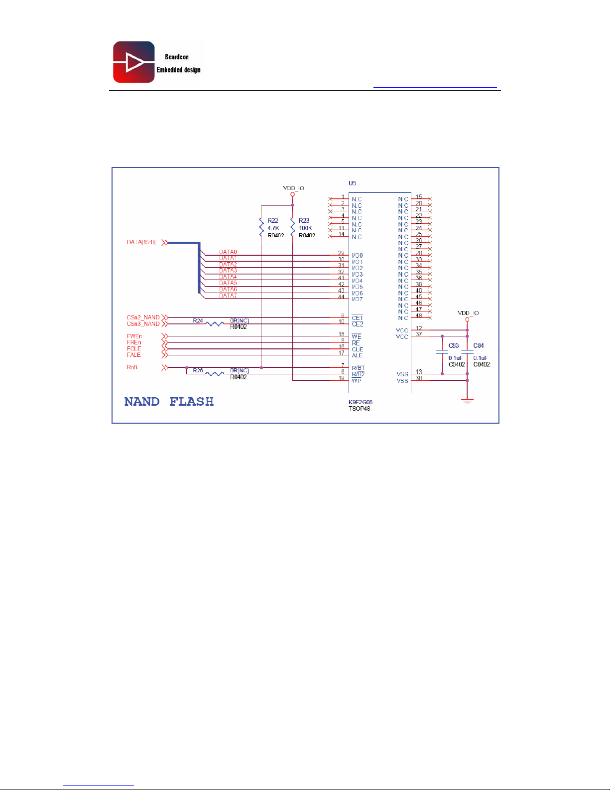
Nand FLASH is a startup device, when startup the main chip S3C6410 automatically copy
the former 8K bites code in Nand Flash to the chip’s internal Stepping Stone room for
running. After initialization configuration, the chip jumps to start address of Kernel to run
the OS. Below picture shows the schematic drawing of Nand Flash:
3.2. DDR RAM
The IDEA6410 adopts two Samsung K4X51163PC 64M Bytes Mobile DDR RAM with
266MHz. They are small BGA package in order to save the room of the board, also is to
use same length circuit line on the PCB for guaranteeing the board running with high
speed and stably.
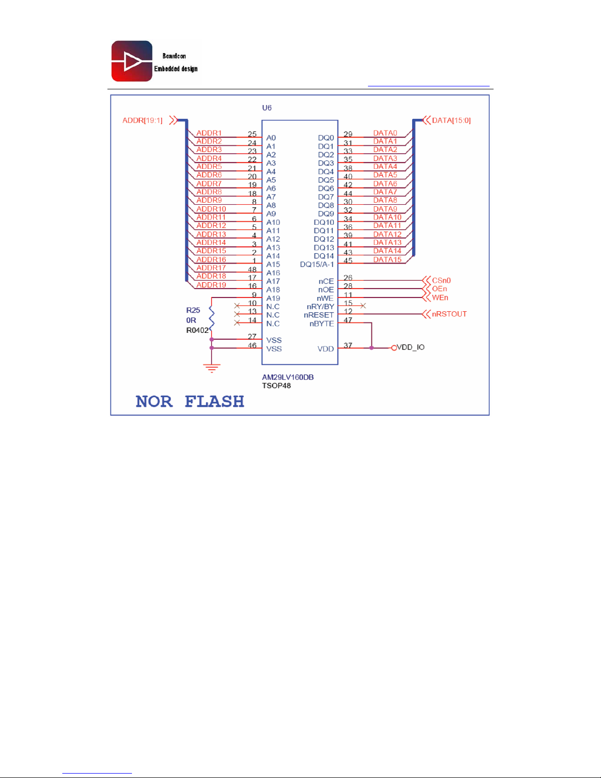
3.3. Nor Flash
IDEA6410 adopts ARM AM29LV160DB Nor Flash, the chip S3C6410 maximum supports
27 pieces address singals A0-A26, in which A20-A26 is reused with DDR data signals
D20-D26. As IDEA6410 adopted 32bit DDR RAM, there are only 19 pieces line A1-A19 for
NOR Flash use. Nor Flash addressing range is 1M Bytes.
Nor Flash can be configured as startup device, it adopts 16-bit SROM startup mode.
Below picture shows the schematic drawing of NOR Flash:
IDEA6410 Hardware Reference Guide
15
Page 16
www.armdesigner.com
IDEA6410 Hardware Reference Guide
16
3.4. Serial Interface
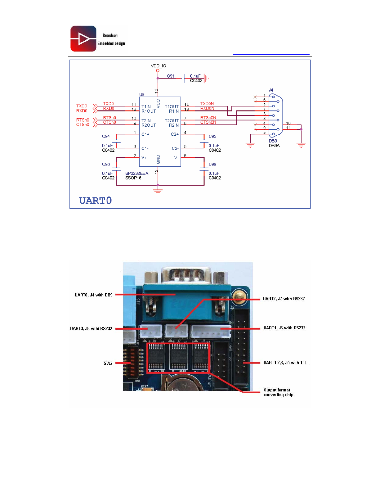
There are four Serial interfaces, UART0, UART1 is 5 lines, UART2, UART3 is 3 lines.
The board uses three pieces SP3232 serial interface chip to change the four serial
interfaces to RS232 level. The user can use switch SW2 to change the output of serial
interface into RS232 or TTL level. There is one piece of standard DB9 port at connector J4,
which is specially design for debugging and printing debugging message. Below picture
shows circuit of UART0
Page 17
www.armdesigner.com
IDEA6410 Hardware Reference Guide
17
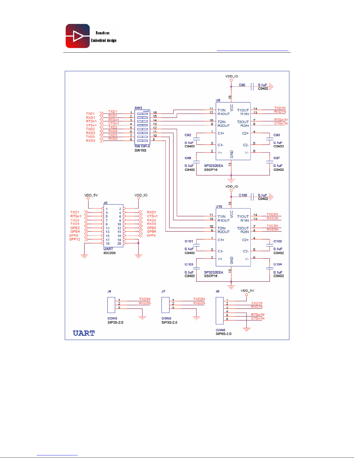
UART1, UART2 or UART3 can be set output into RS232 or TTL by adjusting switch SW2.
The pin header J6, J7, J8 is corresponding to UART1, UART2, UART3 for selecting
RS232 output, pin header J5 is TTL output for UART1, UART2, UART3. Below picture
shows those pin header connectors.
Page 18
www.armdesigner.com
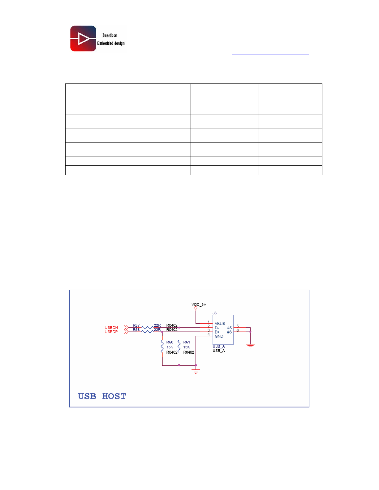
Below picture is circuit drawing of UART1,UAR2,UART3
IDEA6410 Hardware Reference Guide
18
Page 19
www.armdesigner.com
The states of Serial interface output controlled switch SW2, please see below figure
SW2’s corresponding
Place
1-4 bit 5-6 bit 7-8 bit
UART1 TTL output 0 x x
UART1 RS232 output 1 x x
UART2 TTL output x 0 x
UART2 RS232 output x 1 x
UART3 TTL output x x 0
UART3 RS232 output x x 1
Note: It is “1” when SW2 is put on “ON”, it is “0” when SW2 is put on “OFF” , “x” means
that the output can not be fixed.
4. Interface
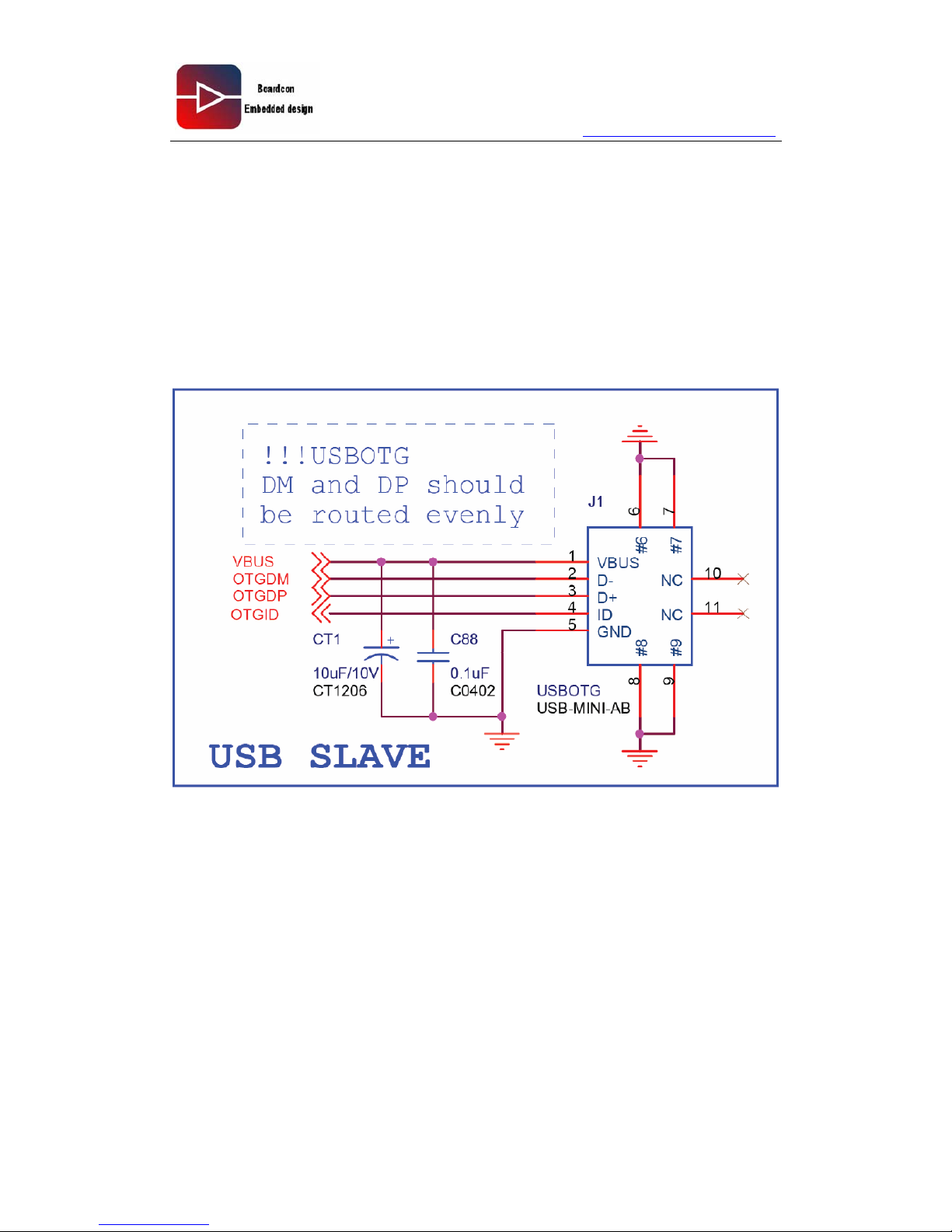
4.1. USB Host
USB Host interface supports USB2.0 Full speed and its port is A type/
The port supports U-Disk, USB Keyboard, USB Portal Disc, USB Mouse.
Below is its circuit drawing of USB Host.
IDEA6410 Hardware Reference Guide
19
Page 20
www.armdesigner.com
4.2. USB OTG
The controller supports the On-The-Go (OTG) feature. The Universal Serial Bus OTG is a
device capable to initiate the session, control the connection and exchange
Host/Peripheral roles between each other.
USB OTG supports USB 2.0 protocol, it supports High speed(480Mbps), Full
speed(12Mbps), low speed(1.5Mbps) data rates. The IDEA6410 default runs on high
speed and slave mode for conveniently connecting with PC. It can use USB OTG to
download program or application when the user in the development.
The USB OTG port type is Mini A/B, below picture is its circuit drawing.
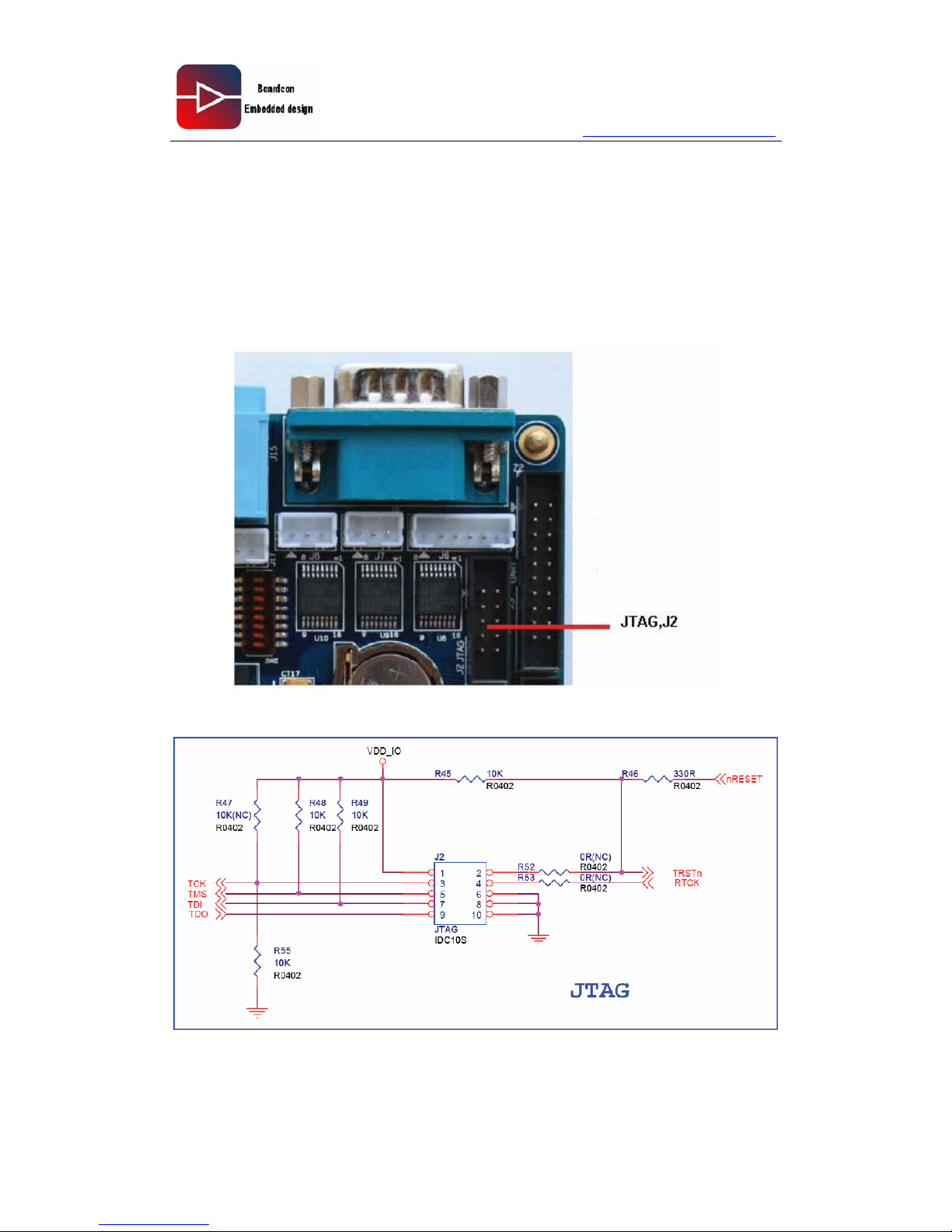
4.3. JTAG
The IDEA6410 is equipped with a JTAG interface for downloading program code into the
external flash, internal controller RAM or for debugging programs currently executing. The
JTAG interface extends out to a 5*2 2.0mm pitch pin header J2. Via configuring the signal
DBGSEL the user can select to operate external Flash or internal controller RAM, below is
the detail configuration of signal DBGSEL.
. When DBGSEL is set as high level, JTAG connects internal controller RAM and can
call on the address of internal controller SRAM.
. When DBGSEL is set as low level, JTAG connects external flash for debugging
programs.
IDEA6410 Hardware Reference Guide
20
Page 21
www.armdesigner.com
Below picture shows the circuit drawing of JTAG.
IDEA6410 Hardware Reference Guide
21
Page 22
www.armdesigner.com
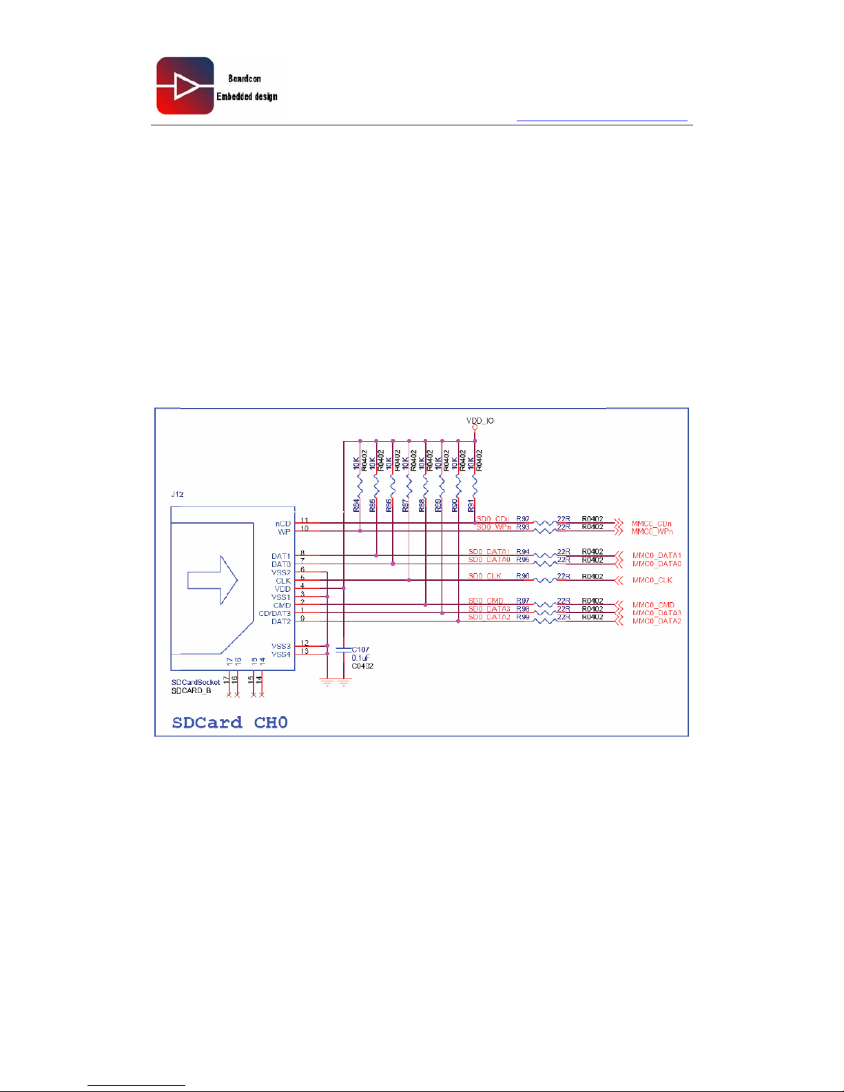
4.4. SD Card
SD Card port J12 supports SD Memory protocol 2.0 and SDIO protocol 1.0. As SD
Memory it can support up to 8G SD card, as SDIO it can support WIFI, GPS Module.
Also the SD Card can be taken as startup device for easily mass production and software
update. About detail configuration please see the chapter 3.5.
Below picture shows the circuit drawing of SD Card.
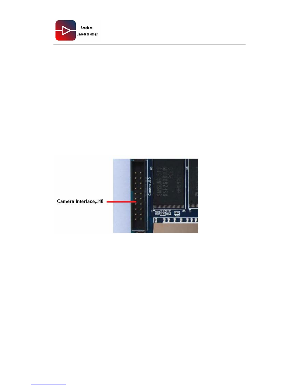
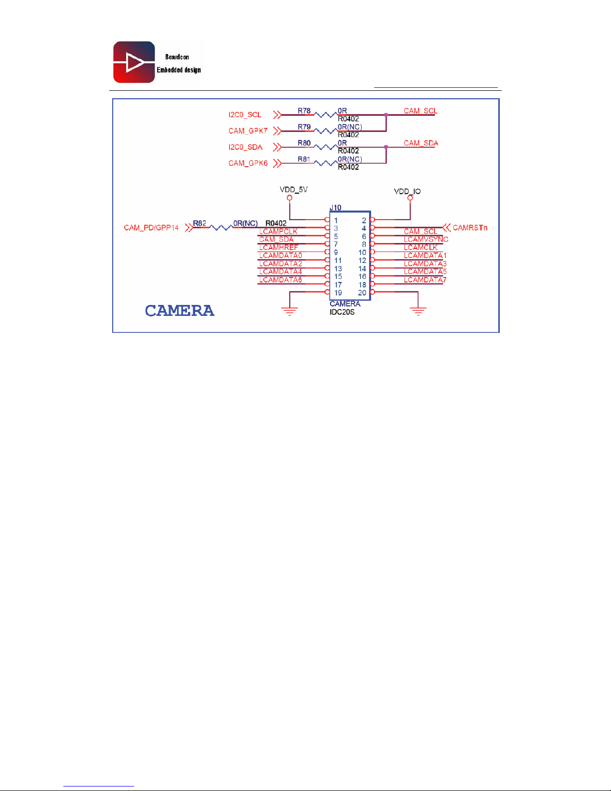
4.5. Camera interfaces
The camera interface supports 8bit ITU-R BT 601/656 mode and resolution up to
4096x4096 dots. The camera interface is a kind of 10*2 pin header connector at J10. The
interface not only has camera signal led out from CPU controlled but also has been added
signal IIC and CAM_PD/GPP14(GPIO). In normally the camera device is set by IIC, but
we added CAM_PD/GPP14 to protect IIC clashed with other external devices, once
happened this case, the CAM_PD/GPP14(GPIO) can replace IIC.
Also added CAM_PD/GPP14 for camera device power management like power off, power
save management and so on.
Boardcon developed a camera module which can directly connect with the board, and its
IDEA6410 Hardware Reference Guide
22
Page 23
www.armdesigner.com
resolution up to 1.3M pixels. More information about the Module, please refer to chapter
5.3.
Below pictures are about Camera interface:
IDEA6410 Hardware Reference Guide
23
Page 24
www.armdesigner.com
IDEA6410 Hardware Reference Guide
24
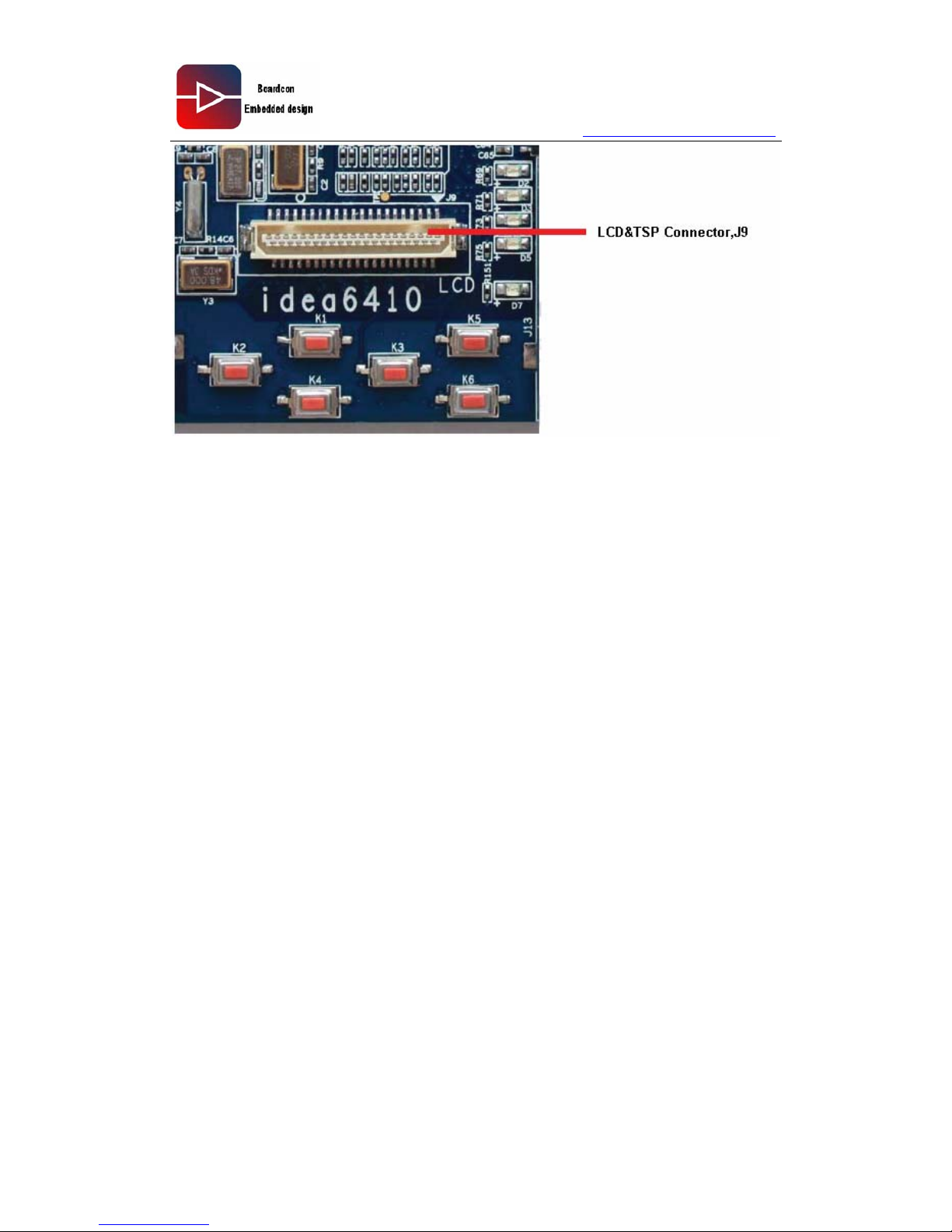
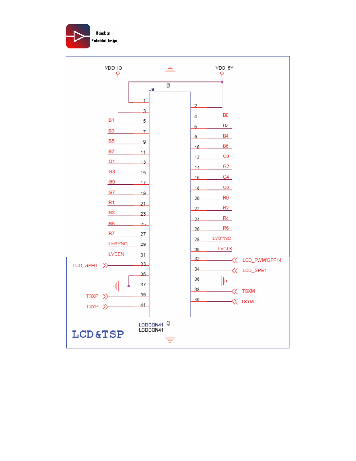
4.6. TFT LCD and Touch Screen interface
The default package for the IDEA6410 Single Board Computer contains a piece of LCD
Module, the Module is made from one piece of 4.3inch TFT LCD which spec is Innolux
AT043TN24, one piece of Touch Screen and one piece of converter board. The module is
connected with the board via a 41pin 0.5mm pitch FPC cable at connector J9. The
connector contains 2 GPIO and 1 PWM, IDEA6410 uses PWM to control Black-light, but
the 2 GPIO weren’t used, the user can use 2 GPIO to reset, power management and
many other functions.
Below pictures are about LCD and TC connector.
Page 25
www.armdesigner.com
IDEA6410 Hardware Reference Guide
25
Page 26
www.armdesigner.com
IDEA6410 Hardware Reference Guide
26
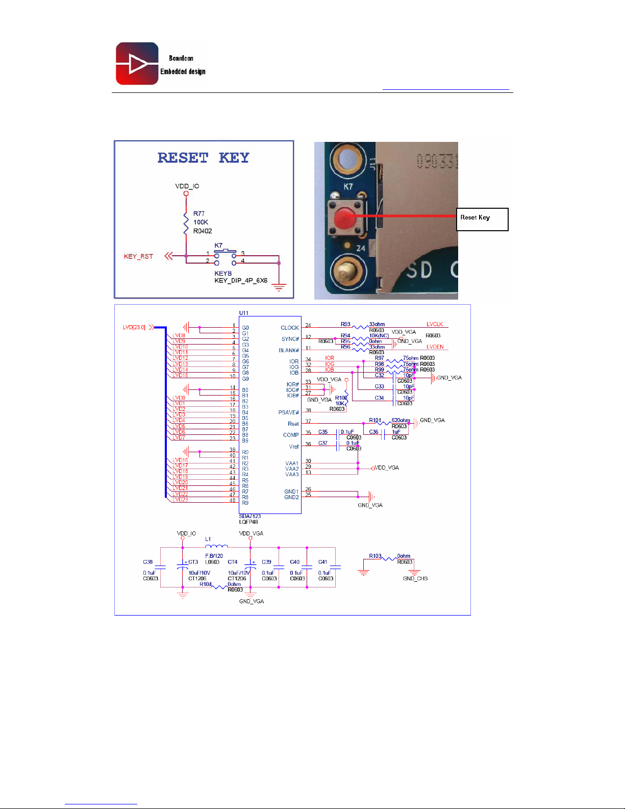
4.7. Reset key
IDEA6410 adopts reset chip MAX811T.
Page 27
www.armdesigner.com
Below pictures are circuit drawing of reset.
IDEA6410 Hardware Reference Guide
27
Page 28
www.armdesigner.com
IDEA6410 Hardware Reference Guide
28
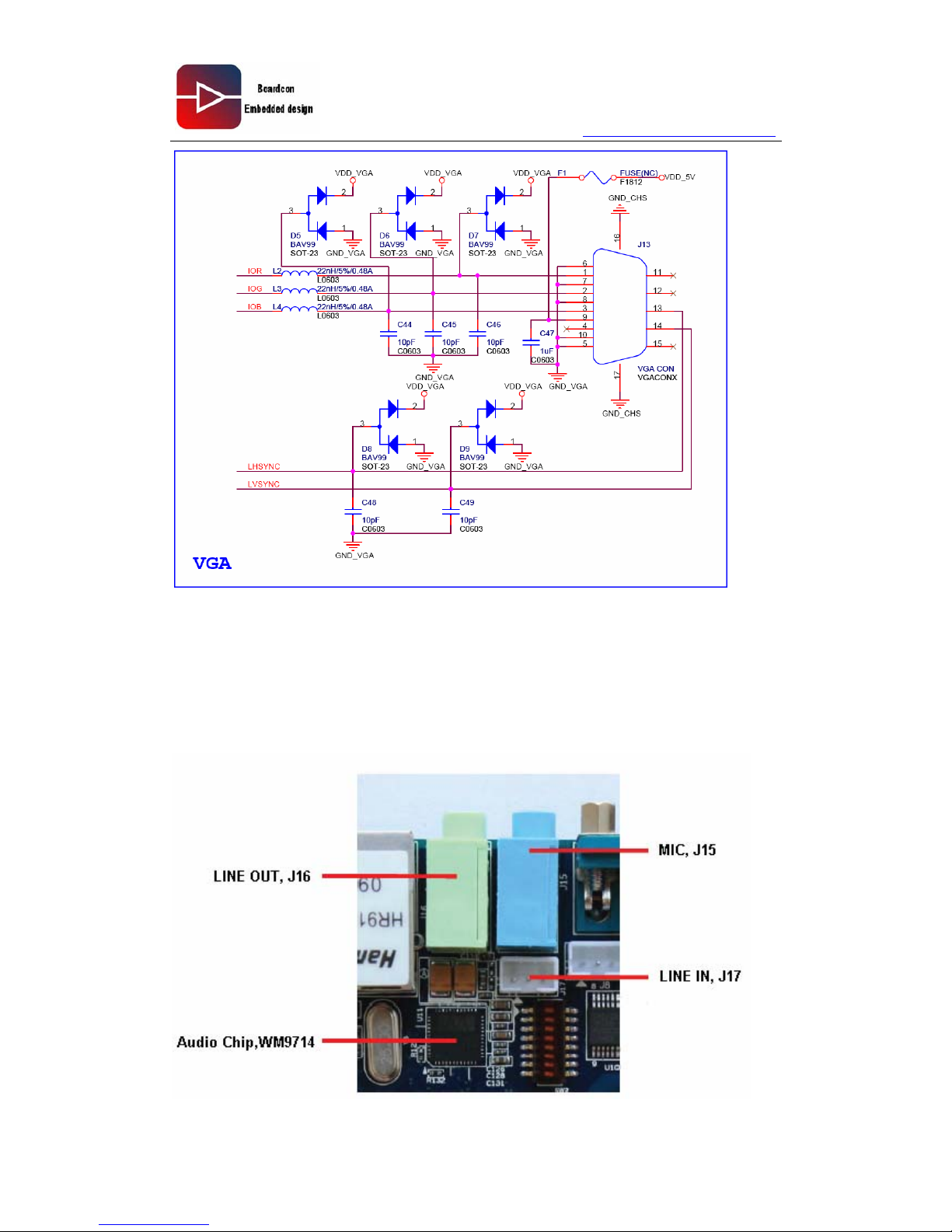
4.8. Audio interface
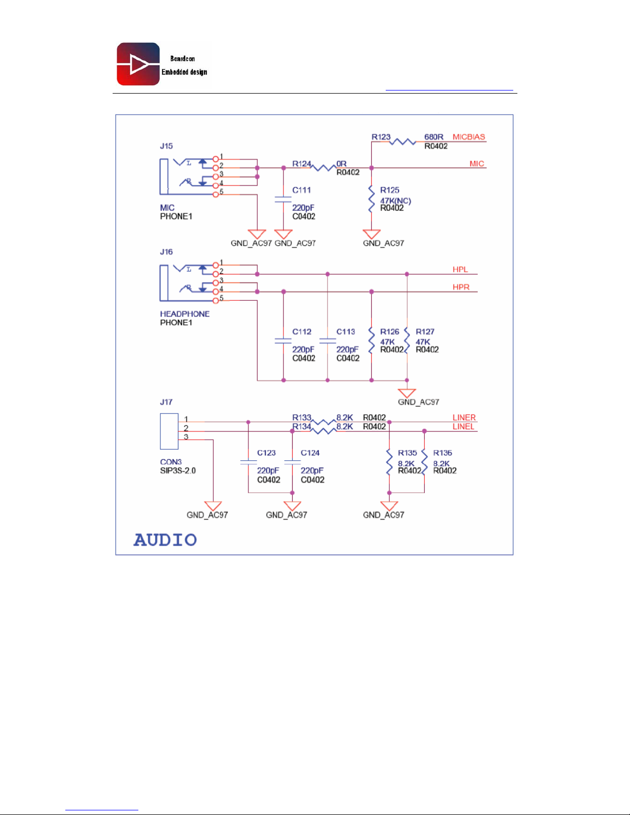
IDEA6410 adopts internal controller AC97 BUS to connect external audio chip WM9714.
The board has connectors Line out(J16), Line in(J17) and MIC in(J15).
Below pictures are about Audio interface.
Page 29
www.armdesigner.com
4.9. Buzzer
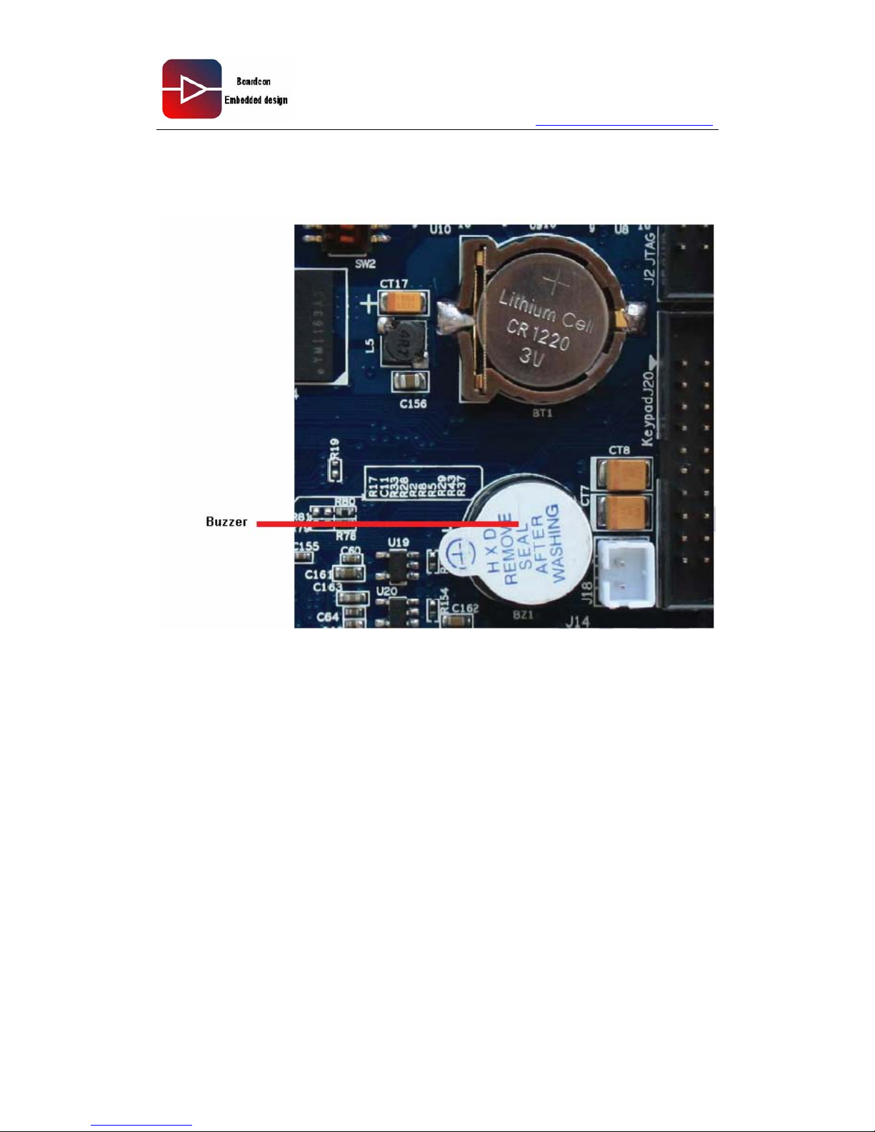
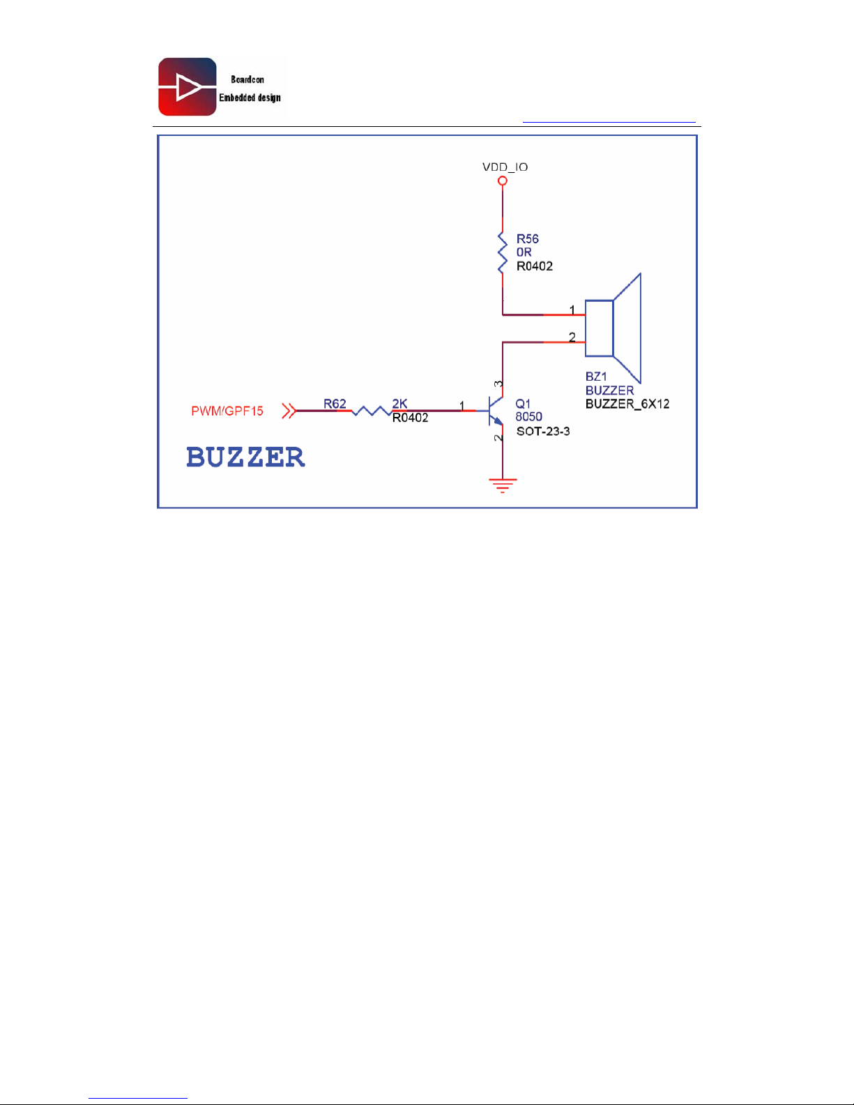
IDEA6410 has one piece of DC Buzzer. It adopts NPN dynatron SS8050 to amplify the
driver current for buzzer. The buzzer is controlled by signal PWM1_GDF15.
IDEA6410 Hardware Reference Guide
29
Page 30
www.armdesigner.com
Below is circuit drawing about Buzzer
.
IDEA6410 Hardware Reference Guide
30
Page 31
www.armdesigner.com
IDEA6410 Hardware Reference Guide
31
4.10. 100M Ethernet interface
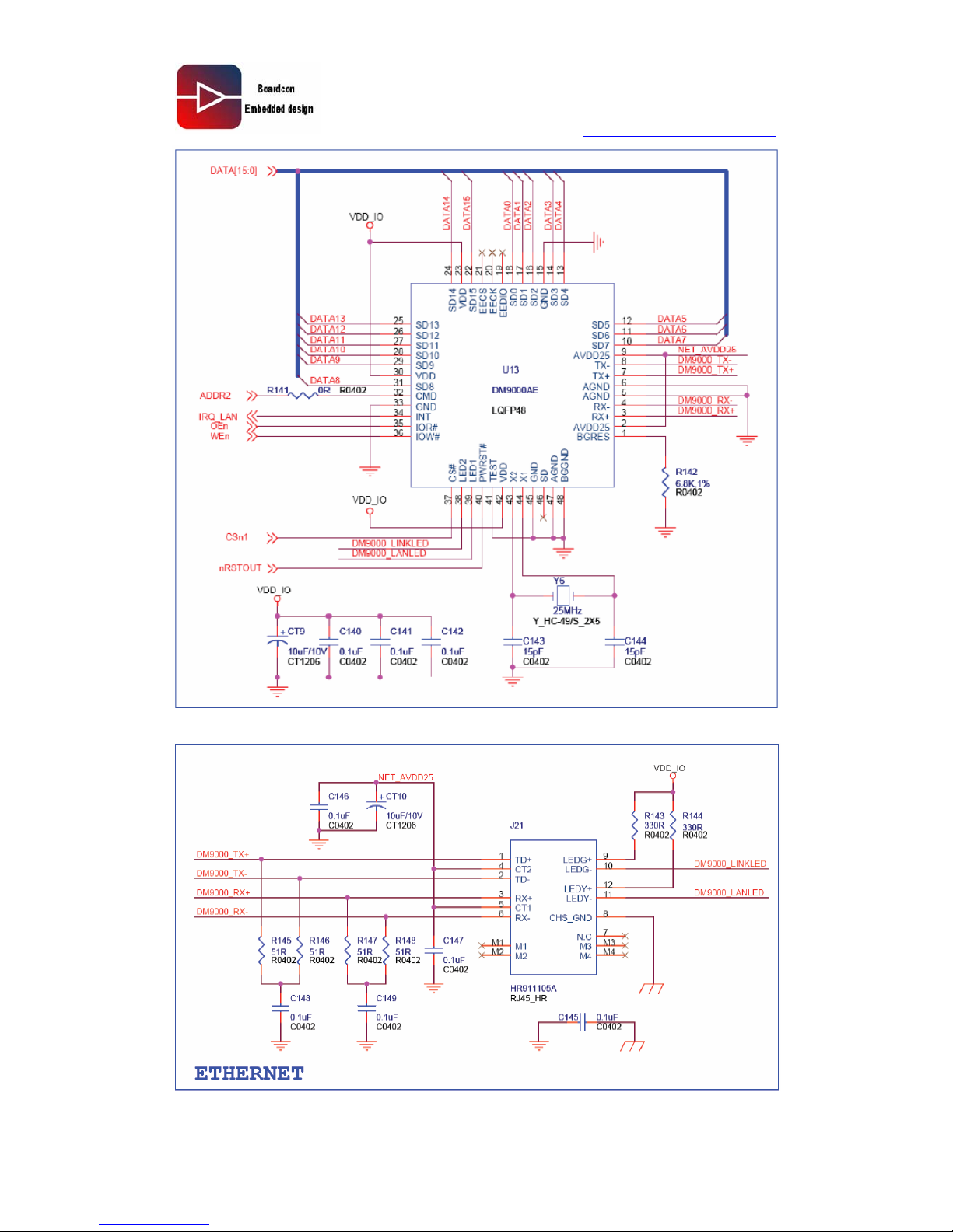
The Ethernet interface is supplemented on the board by the Ethernet Transformer and the
RJ45 connector. The Ethernet controller is external chip DM900AE, the chip call on the
external CPU interrupt signal EINT7
On the process of the development, the interface can connect with PC via cross Ethernet
line to download WinCE Image, Linux Kernel and File System. Below circuit drawing is
about Ethernet interface.
Page 32
www.armdesigner.com
IDEA6410 Hardware Reference Guide
32
Page 33
www.armdesigner.com
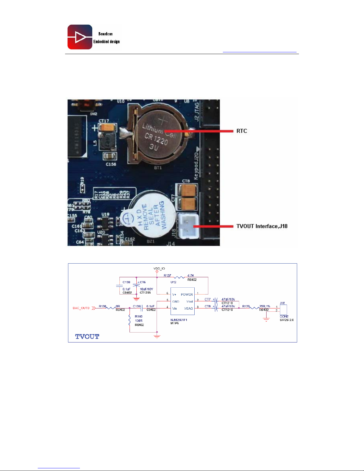
4.12. TVOUT interface
The IDEA6410 has a 2-pin 2.0 pitch TVOUT interface at connector J18. Below pictures
are about TVOUT interface.
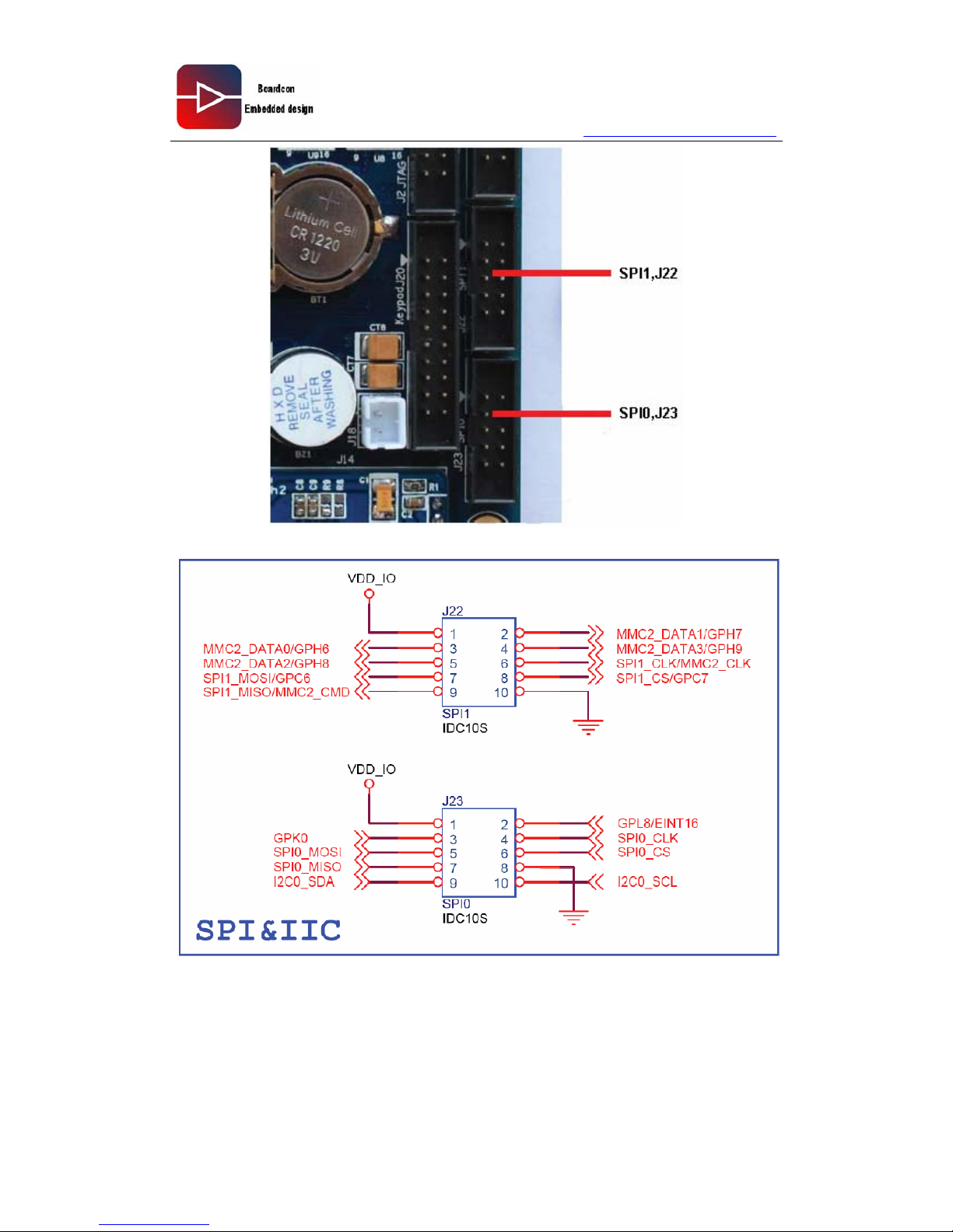
4.11. High Speed SPI, MMC2 and I2C interface
The IDEA6410 has two SPI interfaces and one I2C interface. They adopts 2.0mm pitch
space biserial dip connector J21 and J23, in which J22 contains SPI1 and MMC2, J23
contains SPI0,IIC and GPIO. The SPI1 is reused with MMC2 on the pin of the main chip,
the customer use SPI interface to conveniently debugging WIFI and Digital TV modules.
Below pictures are about SPI, MMC2 and I2C.
IDEA6410 Hardware Reference Guide
33
Page 34
www.armdesigner.com
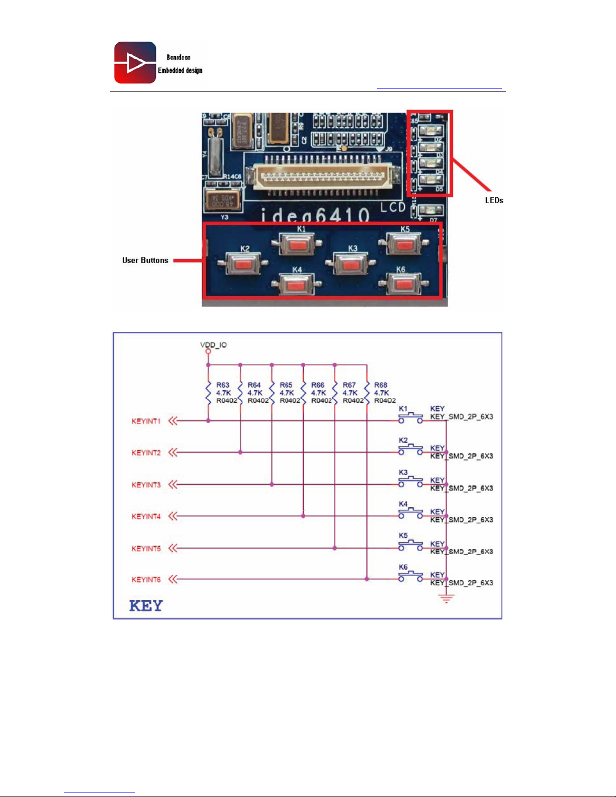
4.12. User Buttons and LEDs
There are 6 pieces of user button, and 4 pieces of LED. User buttons and LEDs are
controlled by GPIO, it accepts interrupt mode and query mode.The user can program
them according to requirement. LED on indicates high level, LED off indicates low level.
IDEA6410 Hardware Reference Guide
34
Page 35
www.armdesigner.com
Below circuit drawing is about them.
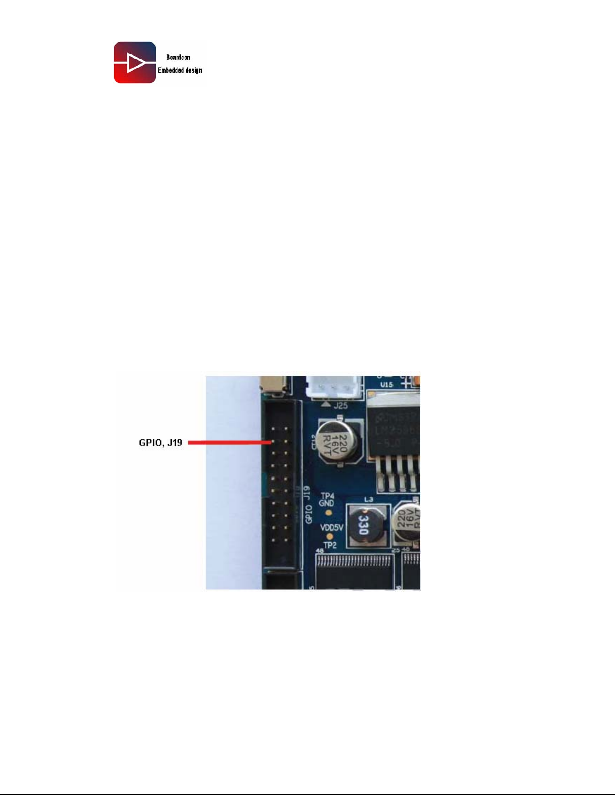
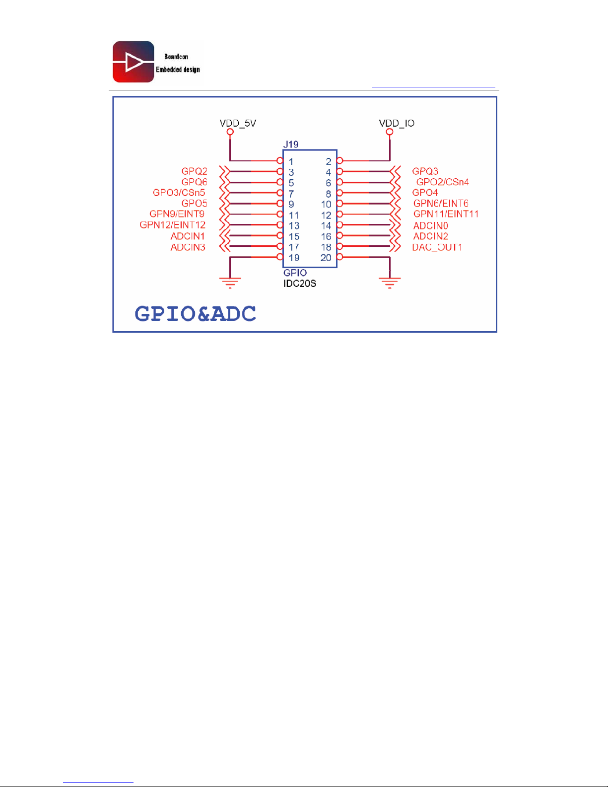
4.13. GPIO and ADC
S3C6410 has totally 186 GPIO. The GPIO can be set as multiplex use, output port , input
port , external interrupt and special function. But this group GPIO K, L, M, N can not be
controlled status under sleep mode, about detail please refer to the chapter GPIO in the
IDEA6410 Hardware Reference Guide
35
Page 36
www.armdesigner.com
data sheet of S3C6410.
The IDEA6410 provide 24 GPIO to the user, in which 11 GPIO are at biserial 10*2 pi n
header connector J25, which also contains 4 ADC and 1 DAC, the customer can use them
according to the requirement. The main chip S3C6410 totally has 8 ADC, in which 4 ADC
ADC4-ADC7 are used to control Touch Screen.
The last GPIO are used in below places:
. 7 GPIO is used at UART interface J2,
. 3 GPIO is used at LCD&TSP connector J9,
. 1 GPIO is used at CAMERA connector J10,
. 2 GPIO is use at SPIO connector J23
Above 18 GPIO is mainly used for LCD, SPI/I2C, BUS connectors, the user also can use
those GPIO for other uses.
Below pictures are about GPIO, ADC
IDEA6410 Hardware Reference Guide
36
Page 37
www.armdesigner.com
IDEA6410 Hardware Reference Guide
37
4.14. RTC
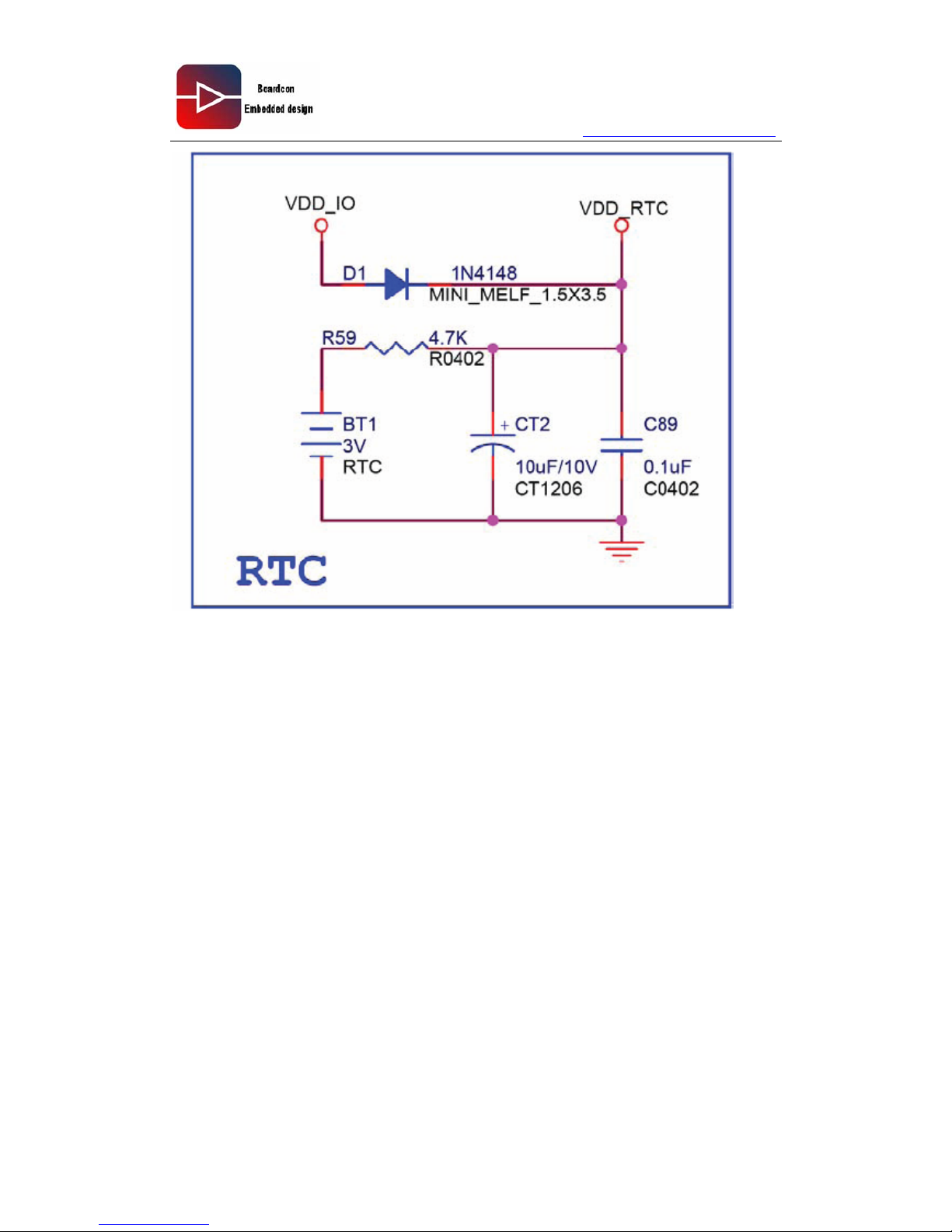
The board is equipped with a battery with type of 1220, when no power supply RTC
provides power VDD_RTC for S3C6410. Below circuit drawing is about RTC.
Page 38
www.armdesigner.com
IDEA6410 Hardware Reference Guide
38
4.15. 8x8 Matrix Keyboard
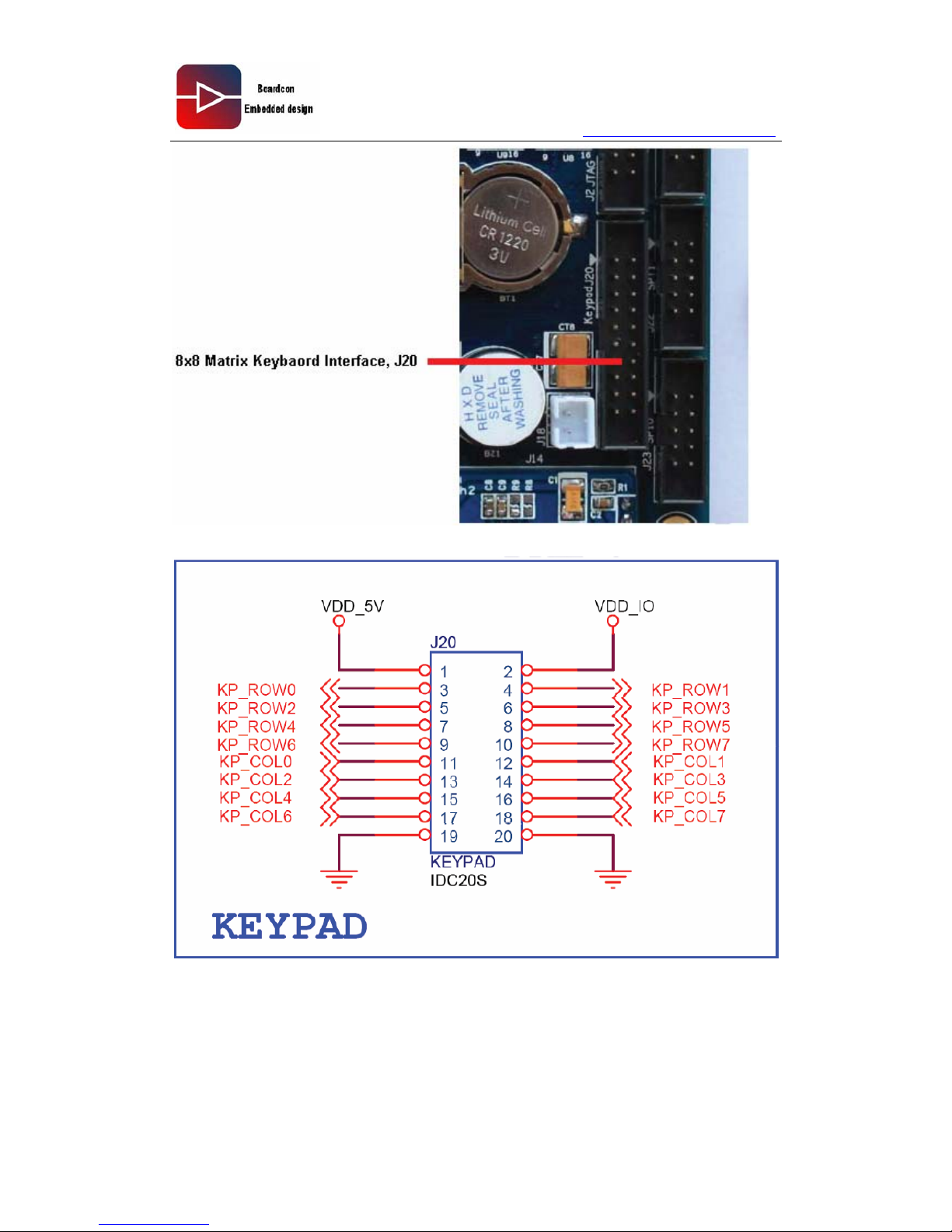
The CPU is built up support matrix keyboard, the maximal limited keys is 8x8. IDEA6410
adopts a biserial 10x2 2.0mm pitch pin header connector J20 for matrix keyboard.
Boardcon developed a 4x4 matrix keyboard which can directly connects with the
connector J20. The 4x4 matrix keyboard also is equipped with a USB_HUB interfaces so
that the user can use it to expand the USB HOST into 4 pieces.
Below pictures are about Matrix Keyboard:
Page 39
www.armdesigner.com
IDEA6410 Hardware Reference Guide
39
Page 40
www.armdesigner.com
5. Optional Modules
5.1. WIFI Module
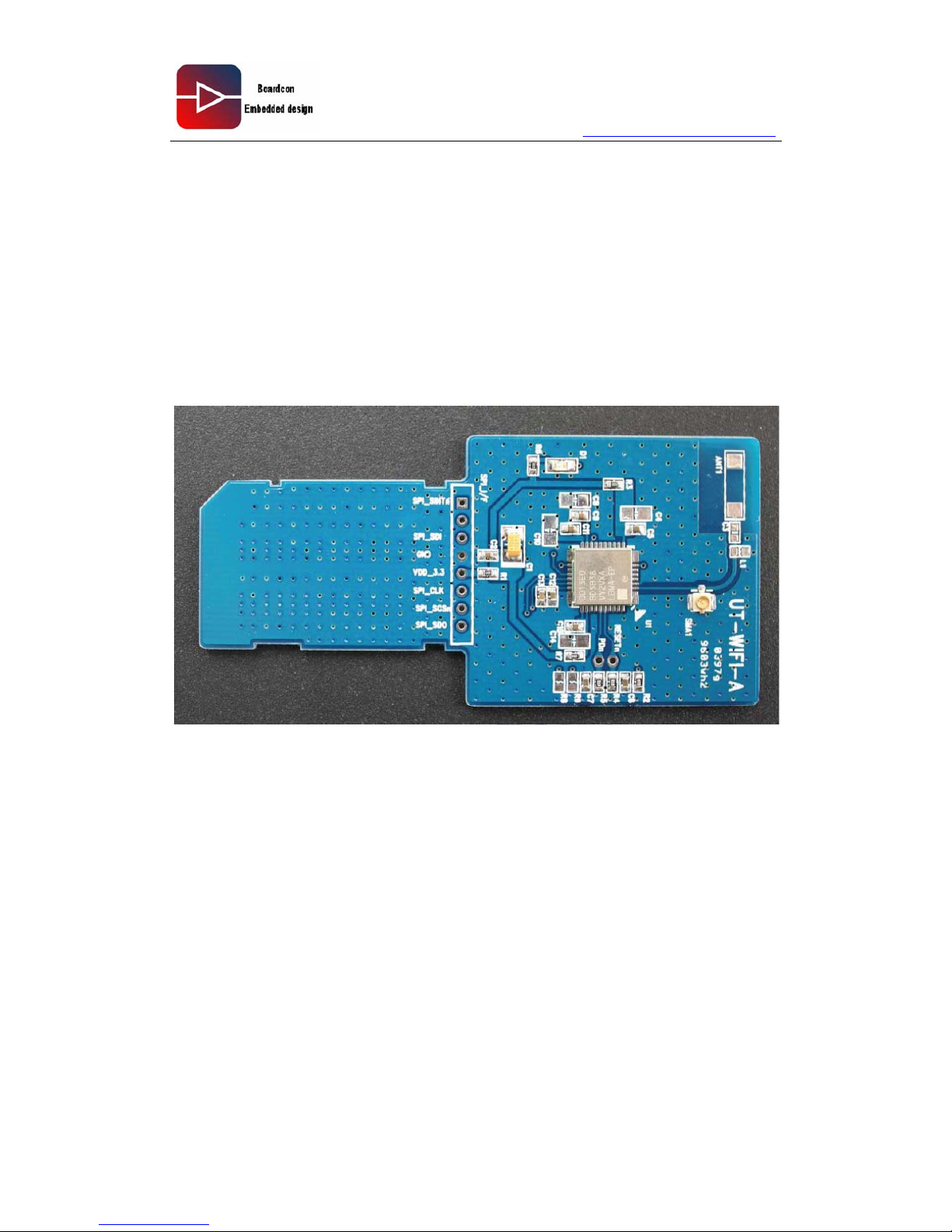
The WIFI Module is connected with the board via SDIO and supports 802.11 b/g protocol.
Now the board supports two kinds of WIFI Chip, one is LBWA18HEPZ-TEMP made from
MURATA , another one is USI-WM-G-MR-09 made from USI. The WinCE6.0 and Linux
2.6.24 driver for WIFI module are available now.
Below is the WIFI Module picture
5.2. GPS Module
The GPS module adopts the chip of SiRF III, its positioning accuracy resolution up to 10m.
5.3. Camera Module
The camera is OV9650 and its resolution up to 1.3M pixel. The module uses 8bit data
mode. The WinCE6.0 and Linux 2.6.24 driver, test program and application are available
now.
5.4. 7 inch TFT LCD Module
Boardcon provides one piece of 7 inch TFT LCD Module for customer choice convenient,
IDEA6410 Hardware Reference Guide
40
Page 41

www.armdesigner.com
IDEA6410 Hardware Reference Guide
41
the Module is made from one piece of 7 inch TFT LCD which spec is Innolux
AT070TN83V.1, one piece of Touch Screen and one piece of converter board. The
module is connected with the board via a 41pin 0.5mm pitch FPC cable at connector J9.
5.5. 4*4 Matrix Keyboard and USB_HUB Module
Boardcon developed 4*4 Matrix Keyboard and USB_HUB Module for the customer choice
and use conveniently. Both devices are connected with the board via a biserial 20-pin 2.0
pitch pace pin header connector.
 Loading...