

Page 1
www.armdesigner.com
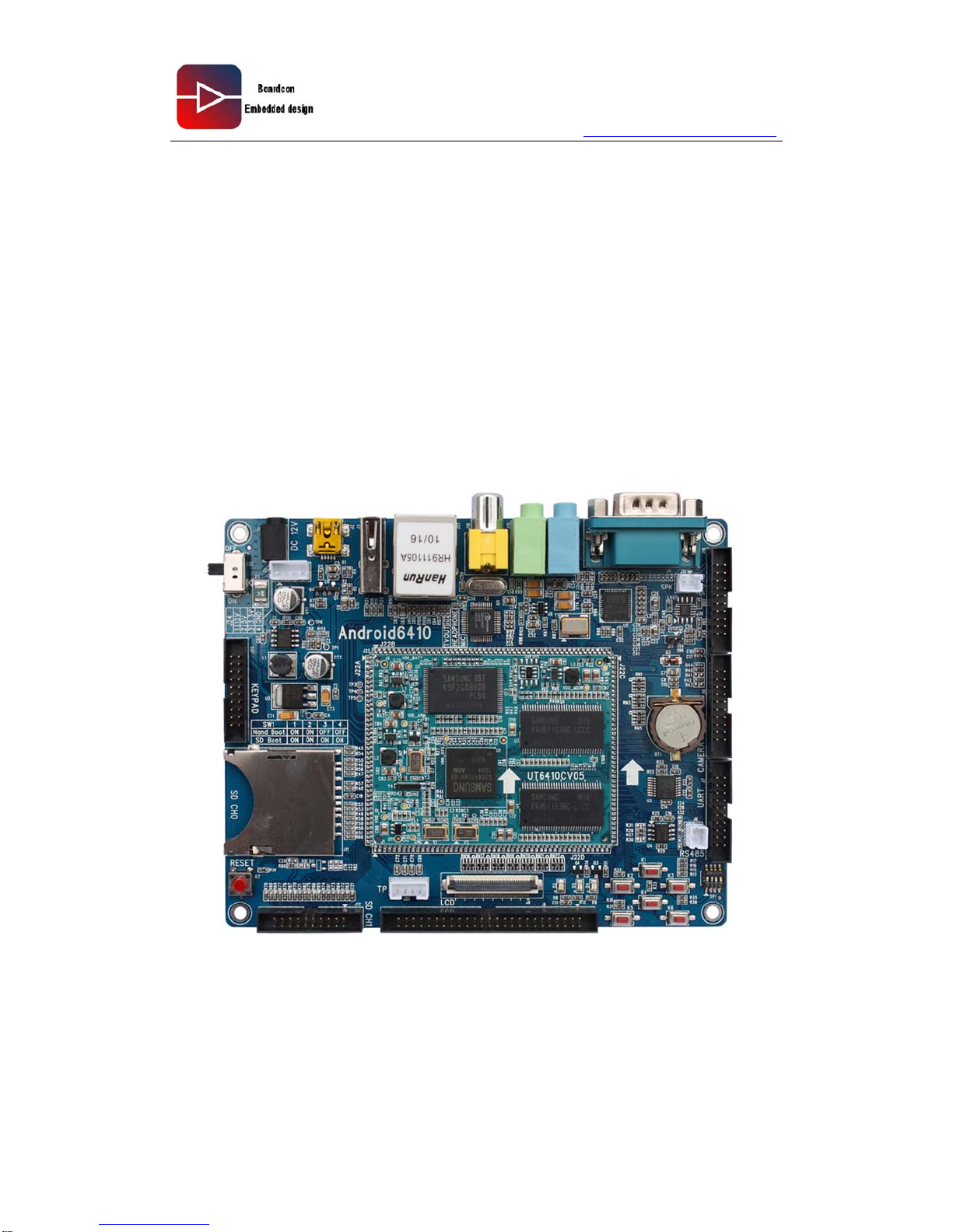
Android6410 Reference Guide
1
Android6410
Single Board Computer
Reference Guide
Page 2

www.armdesigner.com
Android6410 Reference Guide
2
1. Introduction
1.1. About this Manual
This manual is intended to provide the user with an overview of the board and benefits,
complete features specifications, and set up procedures. It contains important safety
information as well.
1.2. Feedback and Update to this Manual
To help our customers make the most of our products, we are continually making
additional and updated resources available on the Boardcon website
(www.armdesigner.com
).
These include manuals, application notes, programming examples, and updated software
and hardware. Check in periodically to see what’s new!
When we are prioritizing work on these updated resources, feedback from customers is
the number one influence, If you have questions, comments, or concerns about your
product or project, please no hesitate to contact us at [email protected]
.
1.3. Limited Warranty
Boardcon warrants this product to be free of defects in material and workmanship for a
period of one year from date of buy. During this warranty period Boardcon will repair or
replace the defective unit in accordance with the following process:
A copy of the original invoice must be included when returning the defective unit to
Boardcon. This limited warranty does not cover damages resulting from lighting or other
power surges, misuse, abuse, abnormal conditions of operation, or attempts to alter or
modify the function of the product.
This warranty is limited to the repair or replacement of the defective unit .In no event shall
Boardcon be liable or responsible for any loss or damages, including but not limited to any
lost profits, incidental or consequential damages, loss of business, or anticipatory profits
arising from the use or inability to use this products.
Repairs make after the expiration of the warranty period are subject to a repair charge and
the cost of return shipping. Please contact Boardcon to arrange for any repair service and
to obtain repair charge information.
Page 3

www.armdesigner.com
Android6410 Reference Guide
3
Catalogue
1. INTRODUCTION................................................................................................................... 2
1.1. ABOUT THIS MANUAL ..................................................................................................... 2
1.2. FEEDBACK AND UPDATE TO THIS MANUAL ............................................................... 2
1.3. LIMITED WARRANTY....................................................................................................... 2
1. ANDROID6410 INTRODUCTION ......................................................................................... 7
1.1. ANDROID6410 INTRODUCTION ........................................................................................... 7
1.2. PRODUCT FEATURES......................................................................................................... 8
2. HARDWARE SOURCES....................................................................................................... 9
2.1 MODULE BOARD INTRODUCTION ......................................................................................... 9
2.1.1 Module Board Parameter Configuration................................................................... 9
2.1.2 Picture of Module Board ......................................................................................... 10
2.1.3 Structure and Size of Module Board........................................................................11
2.1.4 Pin Sequence of Module Board...............................................................................11
2.2 DEFINITION OF MODULE BOARD PIN .................................................................................. 12
2.2.1 Definition of pin of J3 connector ............................................................................. 12
2.2.2 Definition of pin of J1 connector ............................................................................. 12
2.2.3 Definition of pin of J4 connector ............................................................................. 13
2.2.4 Definition of pin of J2 connector ............................................................................. 14
2.2.5 Pin Signal Careful Introduction............................................................................... 15
2.2.6 Core board input voltage / current shows............................................................... 31
2.3. IMAGE OF CARRIER BOARD .............................................................................................. 32
2.3.1 Carrier board structure and layout.......................................................................... 33
3. HARDWARE DESIGN DETAILS ........................................................................................ 33
3.1. POWER SECTION ............................................................................................................. 33
3.1.1. Power input interface............................................................................................. 33
3.1.2 Power switch........................................................................................................... 34
3.1.3 Power LED.............................................................................................................. 34
3.2 START SETTING ................................................................................................................ 34
3.3. DEVICE INTERFACE DESCRIPTION ..................................................................................... 35
3.3.1. MODULE BOARD INTERFACES ........................................................................................ 35
3.3.2 UART asynchronous serial port.............................................................................. 35
3.3.3 USB HOST interface............................................................................................... 36
3.3.4. USB OTG 2.0 Interface.......................................................................................... 37
3.3.5. 100M Ethernet Interface ........................................................................................ 37
3.3.6. SD card Interface................................................................................................... 38
3.3.7. Audio Interface....................................................................................................... 38
3.3.8. TV OUT Interface................................................................................................... 39
Page 4

www.armdesigner.com
Android6410 Reference Guide
4
3.3.9. LCD Interface......................................................................................................... 40
3.3.10. Four-wire resistive touch signal interface ............................................................40
3.3.1 1. CAMERA and IIC Interface.................................................................................. 40
3.3.12. Matrix keyboard interface..................................................................................... 41
3.3.13. High speed SPI and AD Interface........................................................................ 41
3.3.14. User button .......................................................................................................... 42
3.3.15 RTC....................................................................................................................... 43
3.3.16 LED User indicator................................................................................................ 43
3.3.17 Reset Button ......................................................................................................... 43
4. GPIO RESERVED............................................................................................................... 44
4.1. J7UART)..................................................................................................................... 44
4.2. J8(50PIN LCD) ......................................................................................................... 44
4.3. J9(40PIN FPC LCD) ................................................................................................. 45
4.4 J10.(CAMERA).......................................................................................................... 46
4.5 J12.(SDIO MODULE CH1) .......................................................................................... 46
4.6. J22(SPI/AD) ............................................................................................................. 47
4.7. J20(KEYPAD)........................................................................................................... 47
5. WINCE6.0 DRIVE AND INTERFACE TEST....................................................................... 48
5.1. LCD DISPLAY TEST ......................................................................................................... 48
4.3 INCH(480*272) ............................................................................................................. 49
5.2. TV OUT TEST................................................................................................................. 50
5.3. NETWORK PORT TEST...................................................................................................... 52
5.4. AUDIO TEST .................................................................................................................... 54
5.4.1. Audio Output Test...................................................................................................54
5.5. USB TEST ...................................................................................................................... 55
5.5.1. USB HOST Interface Test...................................................................................... 55
5.5.2. USB OTG Interface T est........................................................................................ 56
5.6. SD CARD TEST................................................................................................................ 59
5.7. BUTTON TEST.................................................................................................................. 59
6. WINCE6.0 MULTIMEDIA HARDWARE CODEC TEST...................................................... 60
6.1. TCPMP PLAYER TESTING (HARDWARE DECODING)............................................................ 60
7. TEST HARDWARE ACCELERATION: FILE -> BENCHMARK......................................... 64
6.2. MEDIA PLAYER TEST(DIRECTSHOW FILTERS)............................................................... 66
6.3. RMVB PLAYER TEST....................................................................................................... 68
6.4. FLASH PLAYER TEST ..................................................................................................... 70
6.5. MULTIMEDIA TEST........................................................................................................... 72
6.5.1. Play Movie ............................................................................................................. 74
6.5.2. Play JPEG.............................................................................................................. 75
6.5.3. Play Audio.............................................................................................................. 76
Page 5

www.armdesigner.com
Android6410 Reference Guide
5
6.5.4. T est DirectShow..................................................................................................... 76
6.5.5. T est Multi Decoding................................................................................................ 77
6.5.6. T est Al pha Blend.................................................................................................... 77
6.6. 3DGRAPHICS HARDWARE ACCELERATION TEST(OPENGLES1.1&2.0)........................ 79
6.6.1. OpenGles 1.1 Test................................................................................................. 79
6.6.2. OpenGles 2.0 Test................................................................................................. 81
6.7. JPEG HARDWARE DECODING TEST ................................................................................. 81
7. LINUX DEVICE DRIVER AND INTERFACE TESTING...................................................... 84
7.1. LCD TEST ...................................................................................................................... 84
7.2. TOUCH SCREEN TEST AND CALIBRATION .......................................................................... 85
7.3. SD CARD TEST................................................................................................................ 85
7.3.1. SD card Read Test................................................................................................. 86
7.3.2. SD card Write Test................................................................................................. 86
7.4. USB TEST ...................................................................................................................... 87
7.4.1. USB Mouse T est.................................................................................................... 87
7.4.2. USB Keyboard T est................................................................................................88
7.4.3. U Disk T est............................................................................................................. 88
7.5. NETWORK PORT TEST....................................................................................................... 90
7.6. SERIAL TEST................................................................................................................... 90
7.7. CAMERA TEST................................................................................................................. 92
7.8. AUDIO TEST .................................................................................................................... 92
7.9. VIDEO TEST .................................................................................................................... 93
7.10 IMAGE VIEW TEST....................................................................................................... 93
8. LINUX FUNCTIONAL F MULTIMEDIA HARDWARE CODING......................................... 94
8.1. RUN MULTIMEDIA HARDWARE CODEC TEST PROCEDURES................................................... 94
8.2. H264 VIDEO HARDWARE DECODING TEST........................................................................ 95
8.3. MPEG-4 VIDEO HARDWARE DECODING FUNCTION TEST .................................................. 96
8.4. H263 VIDEO HARDWARE DECODING FUNCTION TEST ....................................................... 97
8.5. VC-1 VIDEO HARDWARE DECODING FUNCTION TESTING................................................... 98
8.6. MULTI-CHANNEL VIDEO TEST HARDWARE DECODING AT THE SAME TIME............................. 100
8.7. JPEG IMAGE DECODING HARDWARE TEST..................................................................... 101
8.8. CAMERA PREVIEW AND H264 VIDEO HARDWARE ENCODING TEST................................... 102
8.9. CAMERA PREVIEW AND JPEG IMAGE HARDWARE ENCODING TEST.................................. 104
8.10. CAMERA PREVIEW AND MFC HARDWARE DECODING TEST............................................ 105
8.11. H264 HARDWARE DECODING AND TV OUT OUTPUT FUNCTION TEST ............................ 105
8.12. MFC HARDWARE DECODING AND CAMERA PREVIEW TV OUT OUTPUT FUNCTION TEST 106
9. LINUX WEB SERVICES TEST...................................................................................................107
9.2. PING COMMAND TEST ................................................................................................... 108
9.3. TELNET FUNCTION TEST................................................................................................ 109
9.3.1. Development telnet Linux Host....................................................................................109
Page 6

www.armdesigner.com
Android6410 Reference Guide
6
9.3.2. T elnet Single Board Computer from Linux Host.........................................................110
Page 7
www.armdesigner.com
Android6410 Reference Guide
7
1. Android6410 Introduction
1.1. Android6410 Introduction
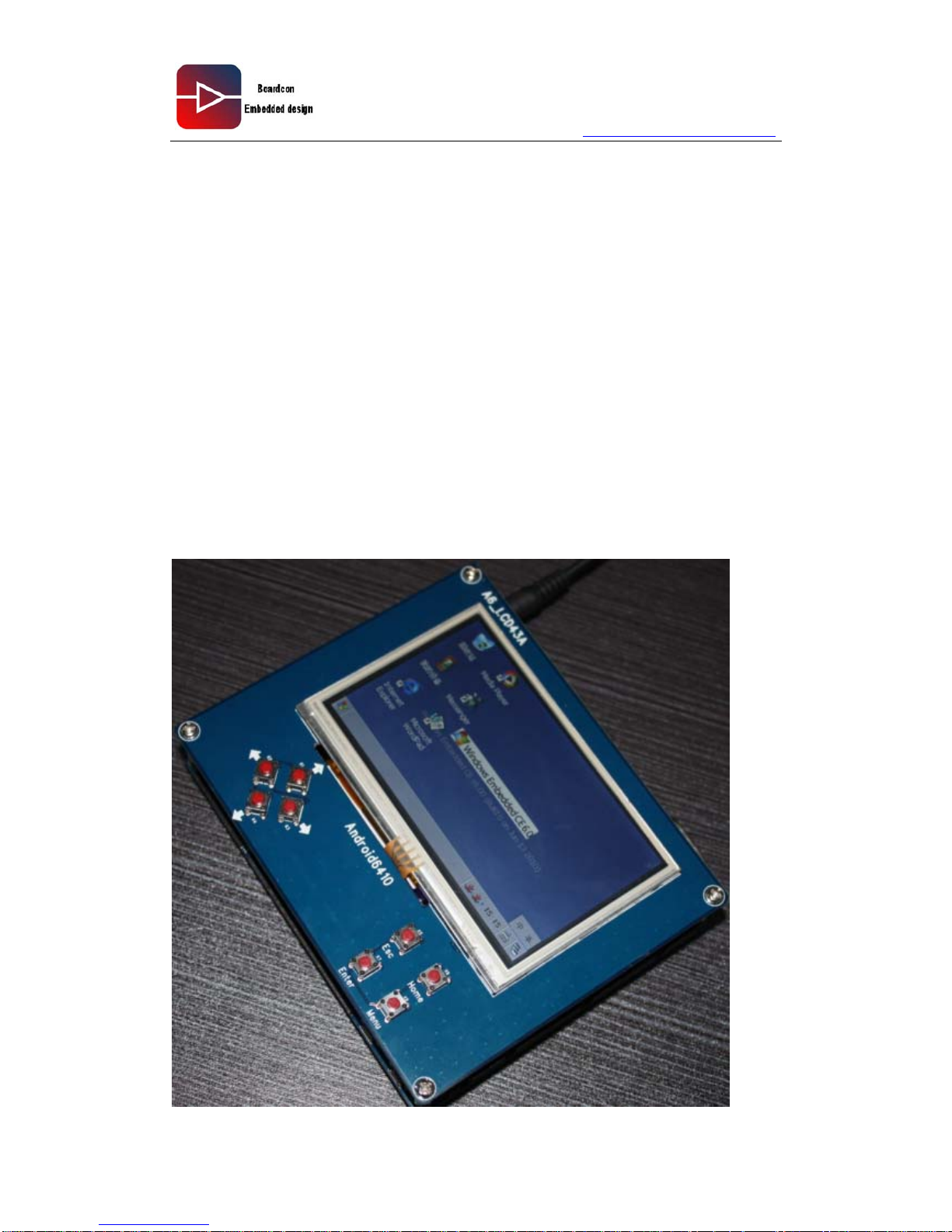
The Android6410 Single Board Computer is developed based on Samsung ARM11, which
is designed to provide cost-effective, low-power capabilities, high performance Application
Processor solution for consumer electronics, industrial control, GPS, industry pda etc...
Mainly for large enterprise users to test, validate, and consult the performance of software
and hardware. Its small, fast, humanized appearance design is a best study tool for high
school, training institutions, the embedded space enthusiasts. Android6410 perfectly
realized the performance of Samsung S3C6410 in video media decoding, 2d the 3d
graphics, display and then put etc... It provides LCD interface, TV Out interface, camera
input port, 4 Serial ports, SD Card interface, SPI, 100m network Ethernet rj45 interface,
USB2. 0 - OTG interface, USB host interface, audio input and output interfaces, i2c
interface etc. it contains a higher CPU Frequency and richer peripheral, and can apply to
the embedded situation which needs higher performance and processing capacity.
Page 8
www.armdesigner.com
Android6410 Reference Guide
8
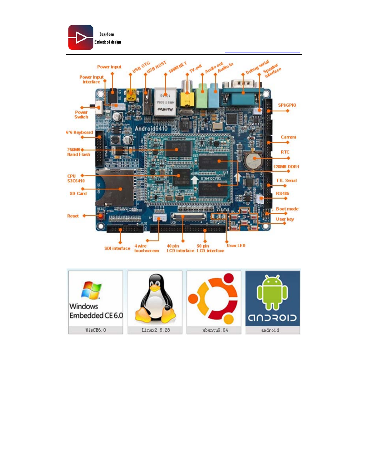
Support the four operating system: WINCE6.0、LINUX、ANDROID、UBUNTU
1.2. Product Features
● Support 667MHz CPU frequency steady operation
● Support WinCE6.0 R2/R3, Linux2.6.28, android2.1 and ubuntu9.04 operating system
● Support 128M/256M DDR1 RAM
● Support MPEG-4/H.264/H263/VC-1 video coding
● Support 2D/3D hardware graphics, TV output
● Support SD/MMC/SDIO smart media card
Page 9
www.armdesigner.com
Android6410 Reference Guide
9
● Support USB2.0 OTG interface download, fast upgrades system
● Support NandFlash, SD card start
● Support 4 road hige speed
serial ports
● Support 4.3inch, 7inch, 10.2inch, 10.4inch or TTL/LVDS etc.
● Support Hive registry preservation
● Support SD card perfect auto upgrade system
● Support TCPMP mplayer perfect hardware decoding, support audio and vedio decoding
under resolution D1
● Support Camera echo, H264/MPEG-4 Video efficiency code
● Support MediaPlayer Video hardware decoding
● Support JPEG images hardware compiling decoding
2. Hardware Sources
2.1 Module Board Introduction
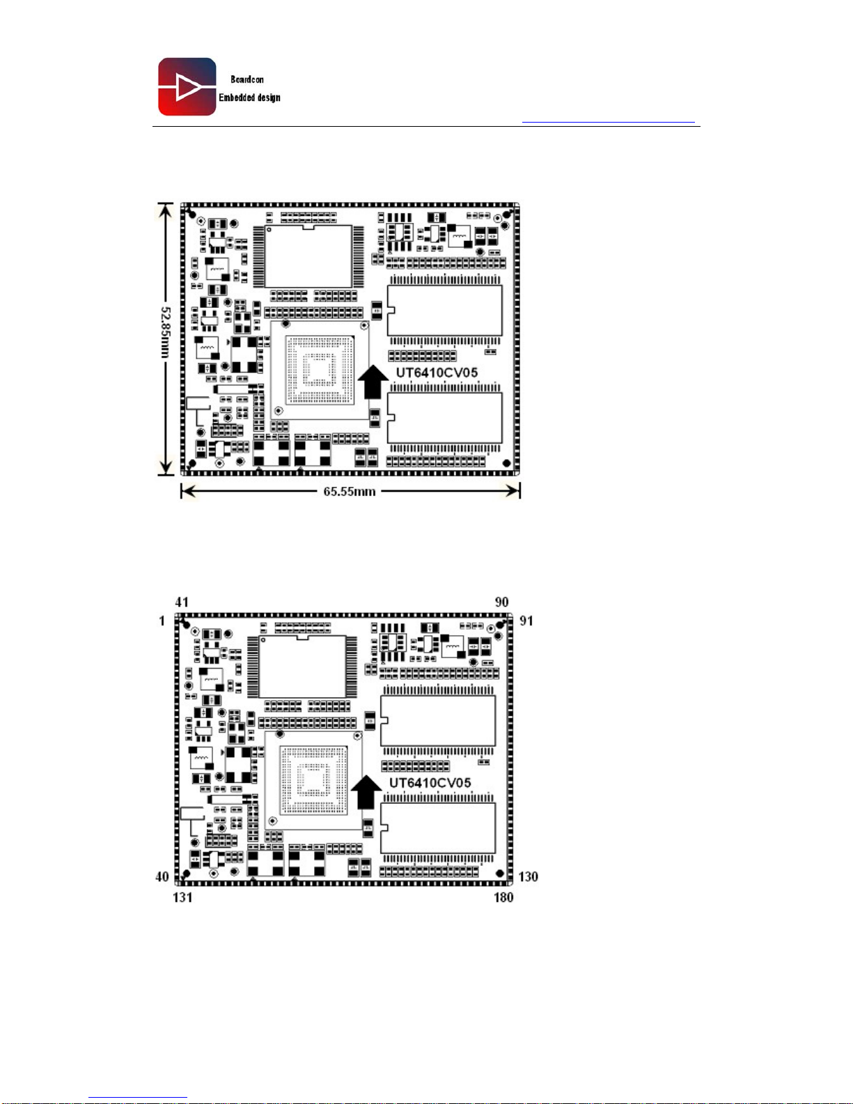
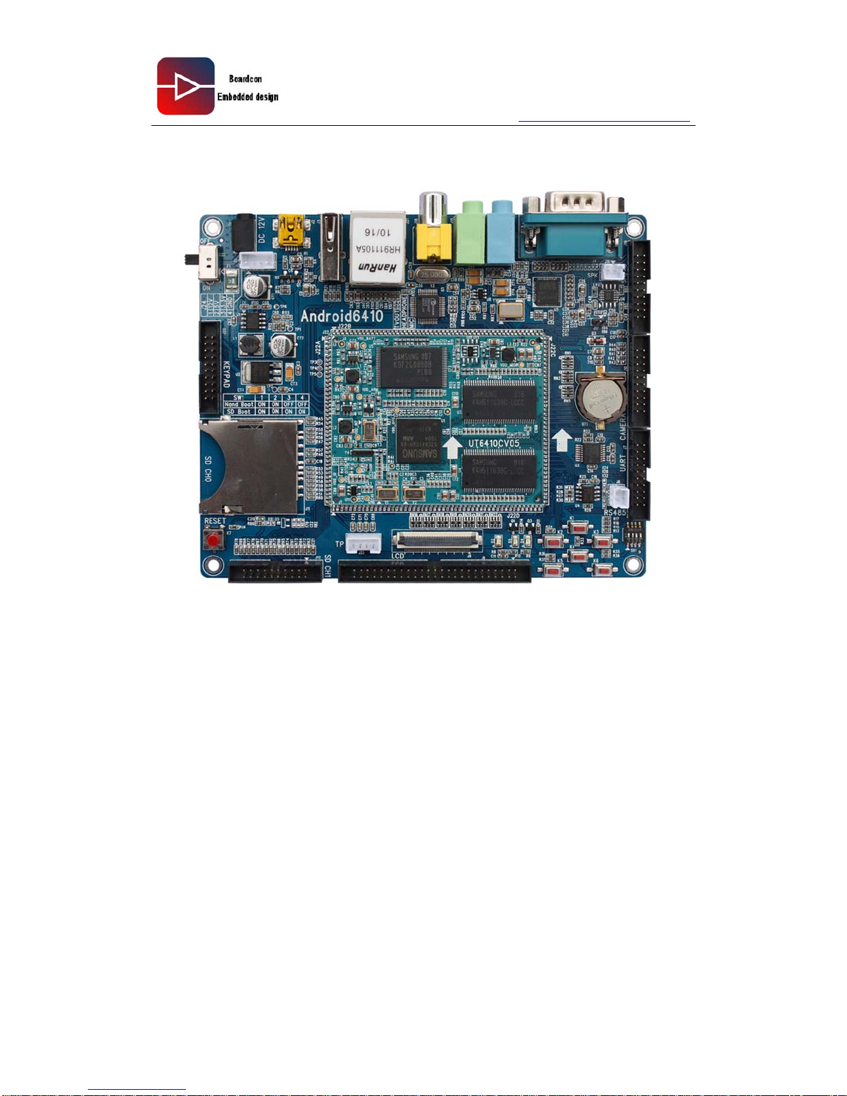
6410CV05 Module Board is a kind of high level of integration, small size, strong scalability,
low TD, high performance module board based on ARM11. Its streamlining appearance,
powerful functions, and peripheral interface make it become a best choice of vehicle
system, intelligence home, industry PDA, industrial digital control, consumer electronics, a
multimedia terminal etc.
This module board use stamp hole interface, which make its welding more fastness and
stability. The DDR1 memory which encapsulated by TSOP is more of the cost and
performance advantage,hardware support upgrade to 256M Bytes DDR1。
Development kit size: 135mm×110mm
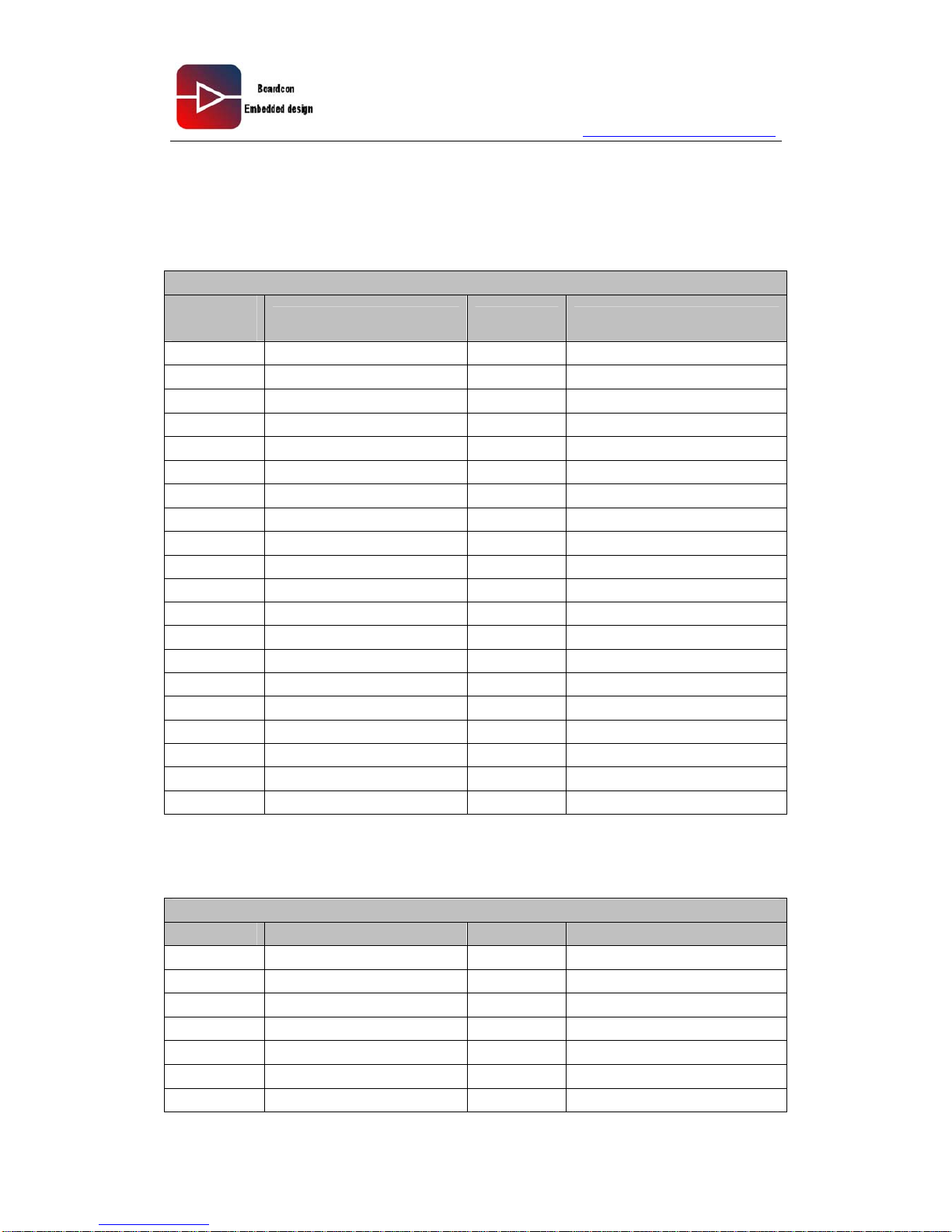
Module board size: 52.85mm×65.55mm
2.1.1 Module Board Parameter Configuration
System configuration
CPU FREQUENCY 667MHz
DDR 128M/256M Bytes DDR1
Nand Flash 256M Bytes
Structure configuration
Appearance
stamp hole character,welding fastness
Size 65.55mm×52.85mm×3mm
Pin spacing 1.27 mm
Page 10
www.armdesigner.com
Android6410 Reference Guide
10
Pin pad size 1.5 mm×0.8 mm
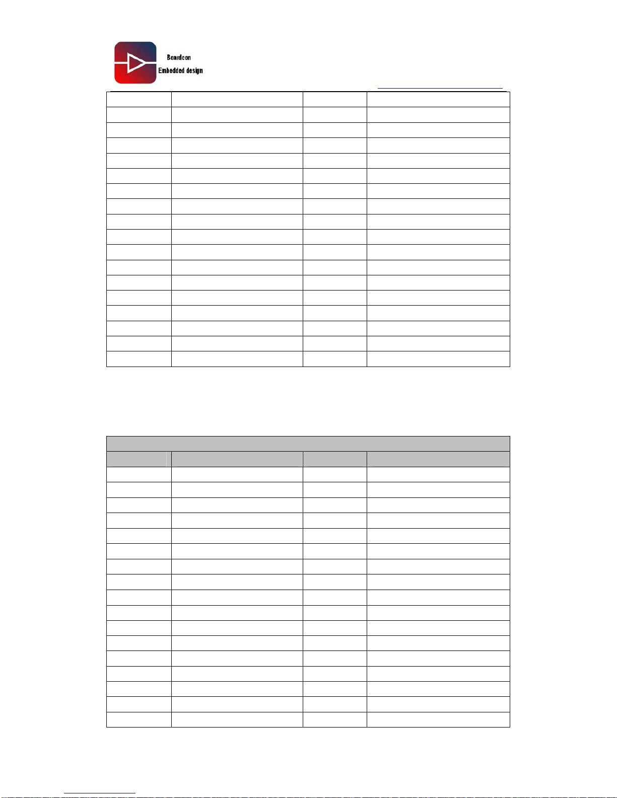
Pin quantity 180
test point The test point is in it
Electric features
Input voltage
3.3V~5V、3V
Working temperature
-10~70℃
Storage temperature
-20~80℃
2.1.2 Picture of Module Board
Page 11
www.armdesigner.com
Android6410 Reference Guide
11
2.1.3 Structure and Size of Module Board
2.1.4 Pin Sequence of Module Board
Page 12
www.armdesigner.com
Android6410 Reference Guide
12
2.2 Definition of Module Board Pin
2.2.1 Definition of pin of J3 connector
Definition of pin of J3 connector
Pin
number
signal Pin number signal
1
VDD_5V
21
SPICS1
2
VDD_5V
22
SD0_DATA0
3
VDD_5V
23
SD0_DATA1
4
VDD_IO
24
SD0_DATA2
5
VDD_IO
25
SD0_DATA3
6
VDD_ARM(NC)
26
SD0_CLK
7
VDD_INT(NC)
27
SD0_CMD
8
VDD_MDDR(NC)
28
SD0_CDn
9
VDD_RTC
29
SD0_WPn
10
GND
30
SD1_DATA0
11
PWRRGTON(NC)
31
SD1_DATA1
12
GPQ0
32
SD1_DATA2
13
OTGID
33
SD1_DATA3
14
OTGDP
34
SD1_CLK
15
OTGDM
35
SD1_CMD
16
VBUS
36
SD1_CDn
17
OTGDRV_VBUS
37
SD1_WPn
18
USBDP
38
GPE0
19
USBDN
39
GPE1
20
SPIMOSI1
40
GPE2
2.2.2 Definition of pin of J1 connector
Definition of pin of J1 connector
Pin number signal Pin number signal
41
GND
66
CSn1
42
GND
67
WEn
43
GND
68
OEn
44
GND
69
DATA0
45
GND
70
DATA1
46
GND
71
DATA2
47
GND
72
DATA3
Page 13
www.armdesigner.com
Android6410 Reference Guide
13
48
GND
73
DATA4
49
GND
74
DATA5
50
GND
75
DATA6
51
ADCIN0
76
DATA7
52
ADCIN1
77
DATA8
53
nBATF(NC)
78
DATA9
54
KEY_RST
79
DATA10
55
GPH9
80
DATA11
56
EINT0
81
DATA12
57
EINT2
82
DATA13
58
OM1
83
DATA14
59
OM2
84
DATA15
60
OM3
85
I2CSCL0
61
OM4
86
I2CSDA0
62
GPH6
87
CAMRSTn
63
nRESET
88
CAMHREF
64
ADDR2
89
CAMVSYNC
65
IRQ_LAN
90
CAMCLK
2.2.3 Definition of pin of J4 connector
Definition of pin of J4 connector
Pin number signal Pin number signal
91
CAMPCLK
111
TXD0
92
CAMYDATA0
112
CTSn0
93
CAMYDATA1
113
RTSn0
94
CAMYDATA2
114
RXD1
95
CAMYDATA3
115
TXD1
96
CAMYDATA4
116
CTSn1
97
CAMYDATA5
117
RTSn1
98
CAMYDATA6
118
RXD2
99
CAMYDATA7
119
TXD2
100
EINT4
120
RXD3
101
EINT9
121
TXD3
102
EINT12
122
GPH7
103
EINT1
123
GPH8
104
EINT3
124
AC97_RSTn
105
EINT5
125
AC97_SDO
106
SPICS0
126
AC97_SDI
107
SPICLK0
127
AC97_BITCLK
Page 14
www.armdesigner.com
Android6410 Reference Guide
14
108
SPIMISO0
128
AC97_SYNC
109
SPIMOSI0
129
GPO2
110
RXD0
130
GPO3
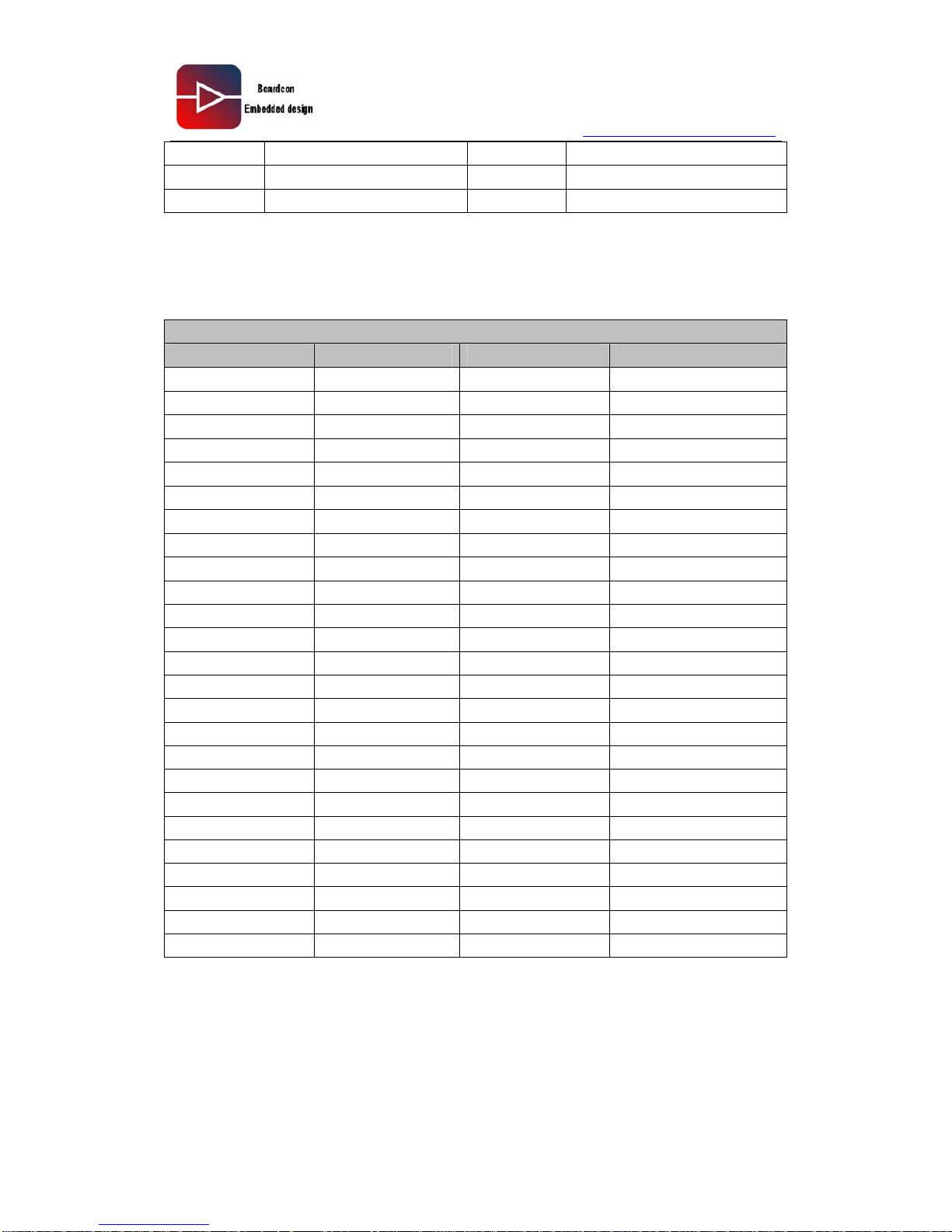
2.2.4 Definition of pin of J2 connector
Definition of pin of J2 connector
Pin number signal Pin number signal
131
TSXM
156
VD7
132
TSXP
157
VD8
133
TSYM
158
VD9
134
TSYP
159
VD10
135
SPIMISO1
160
VD11
136
SPICLK1
161
VD12
137
KP_COL0
162
VD13
138
KP_COL1
163
VD14
139
KP_COL2
164
VD15
140
KP_COL3
165
VD16
141
KP_COL4
166
VD17
142
KP_COL5
167
VD18
143
KP_ROW0
166
VD19
144
KP_ROW1
167
VD20
145
KP_ROW2
170
VD21
146
KP_ROW3
171
VD22
147
KP_ROW4
172
VD23
148
KP_ROW5
173
VSYNC
149
VD0
174
HSYNC
150
VD1
175
VCLK
151
VD2
176
VDEN
152
VD3
177
PWM_TOUT1
153
VD4
178
GPE3
154
VD5
179
GPE4
155
VD6
180
DAC_OUT0
Page 15
www.armdesigner.com
Android6410 Reference Guide
15
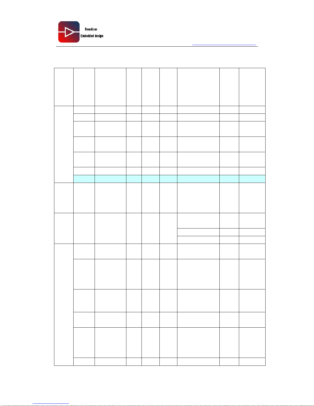
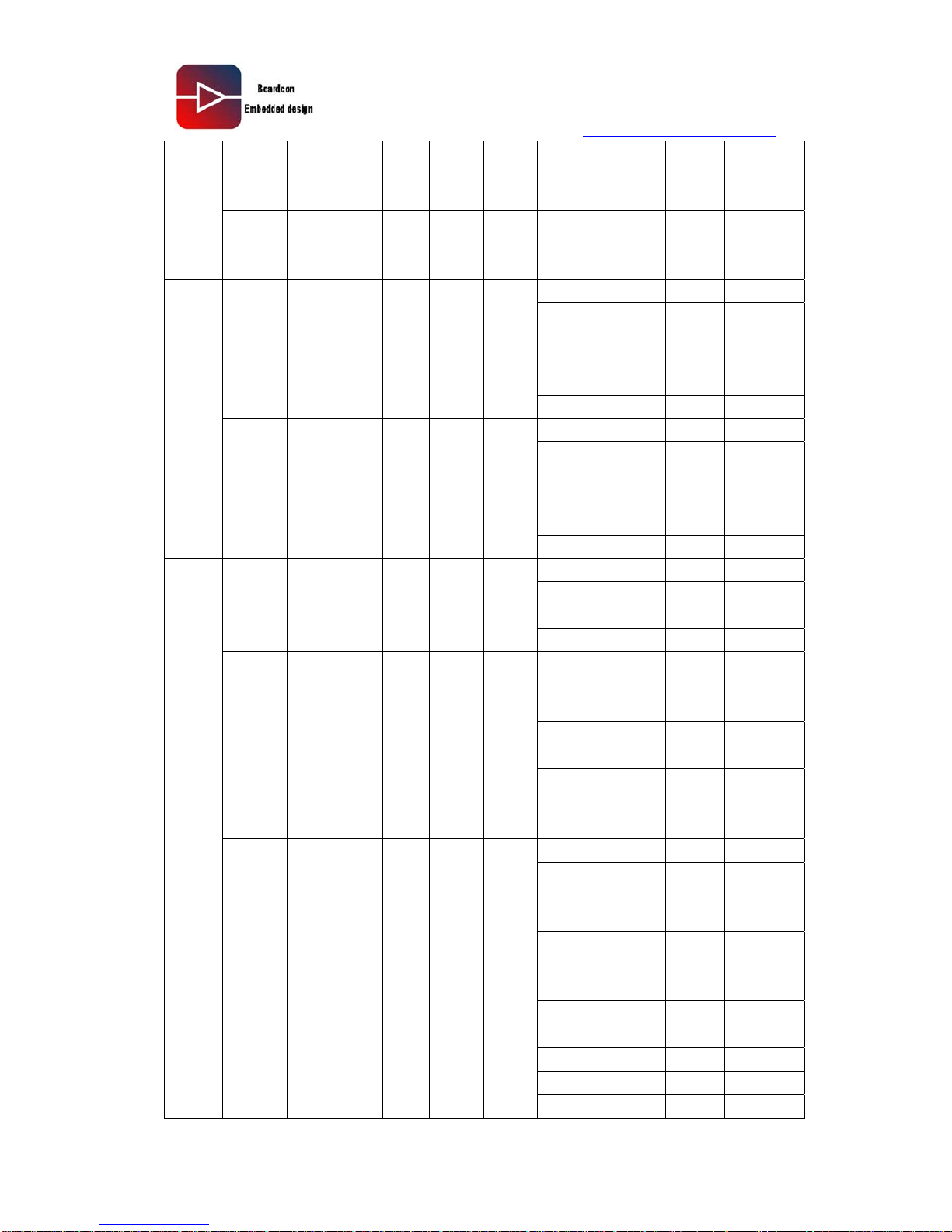
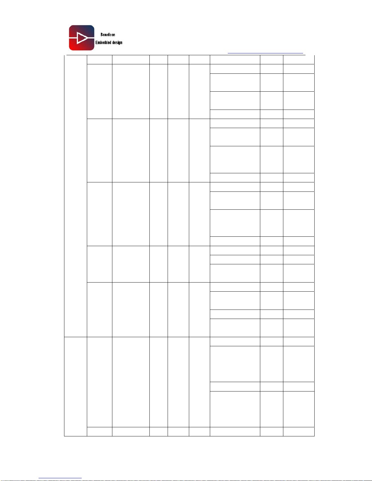
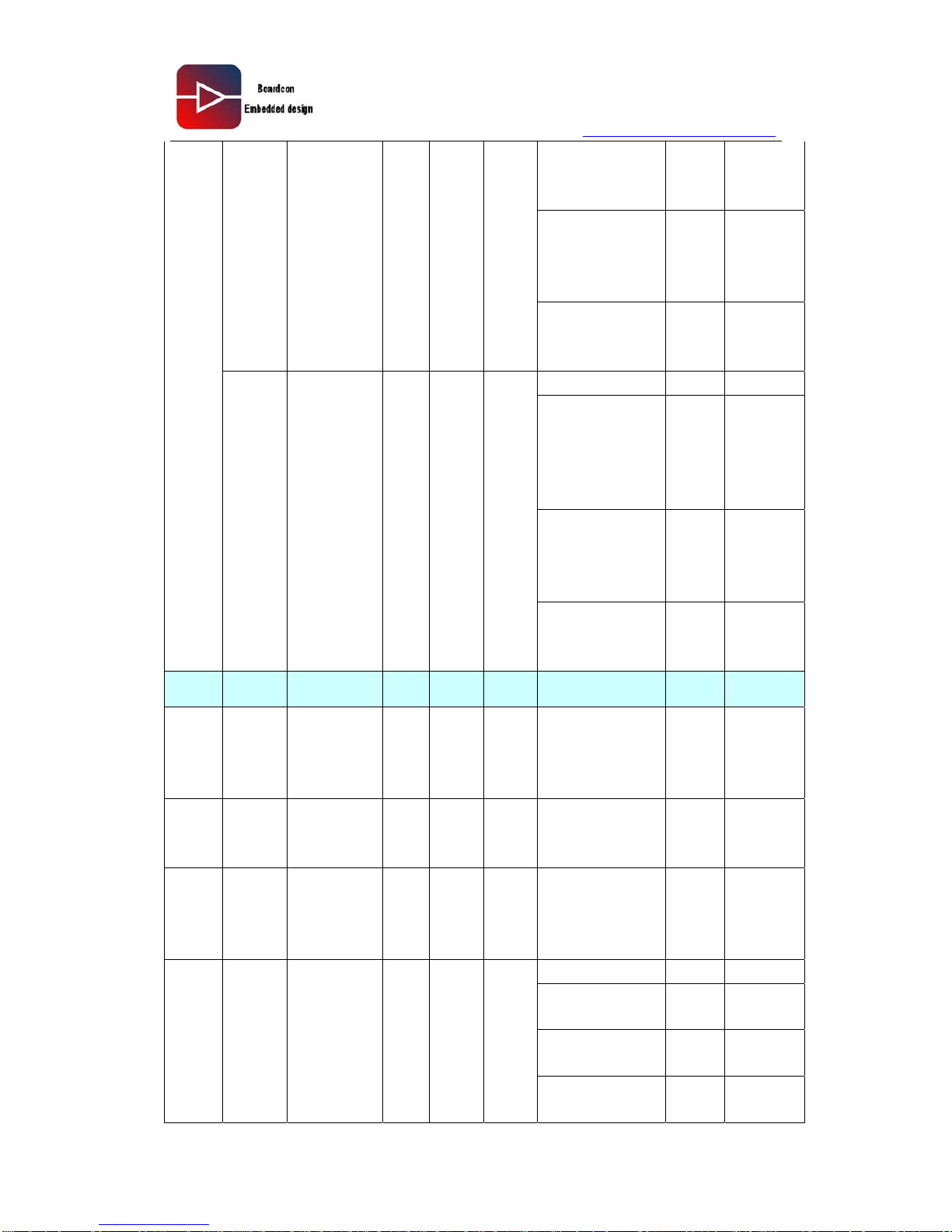
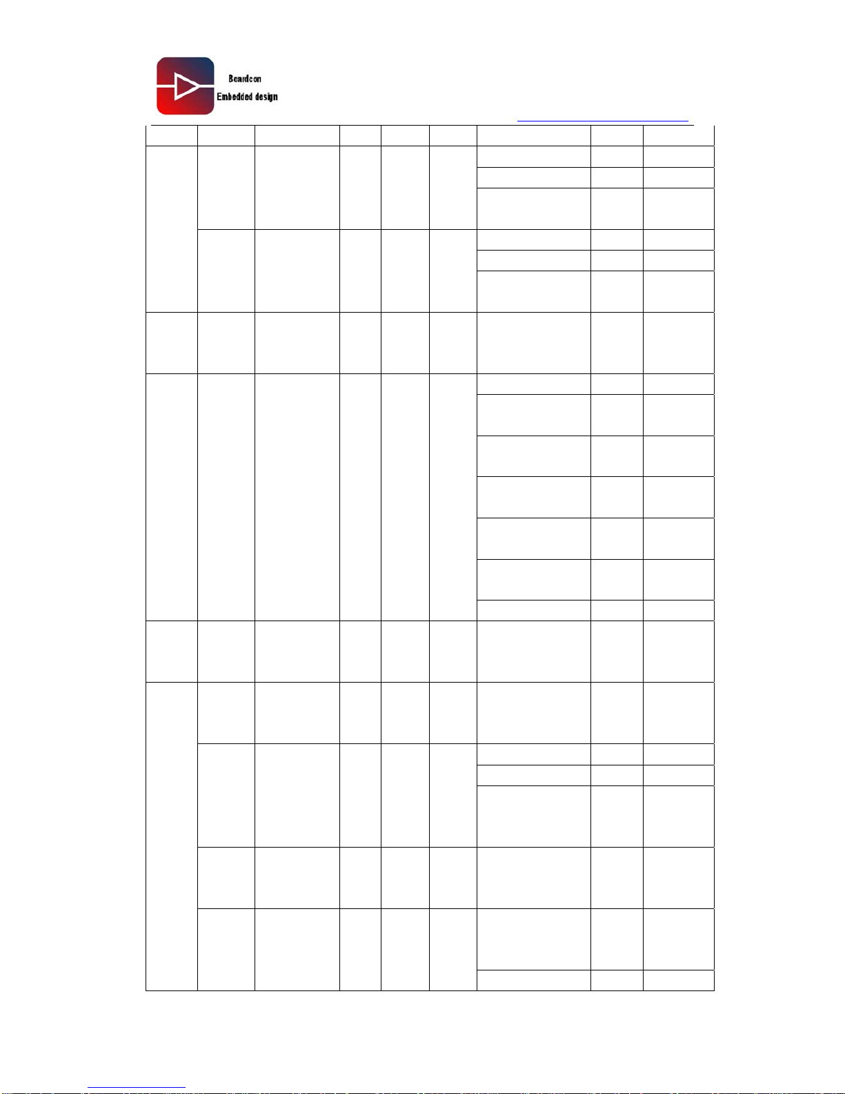
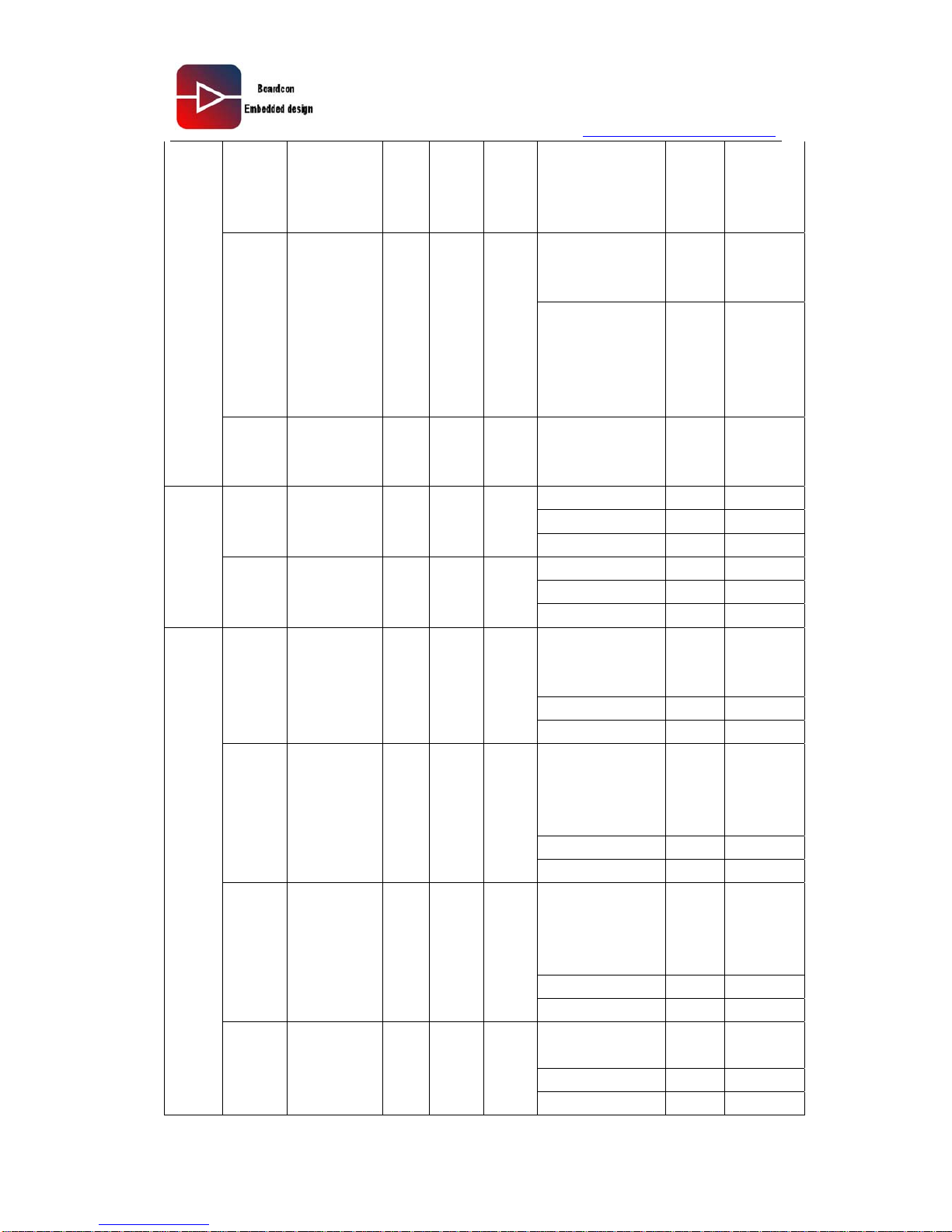
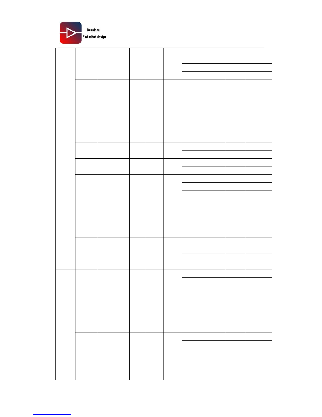
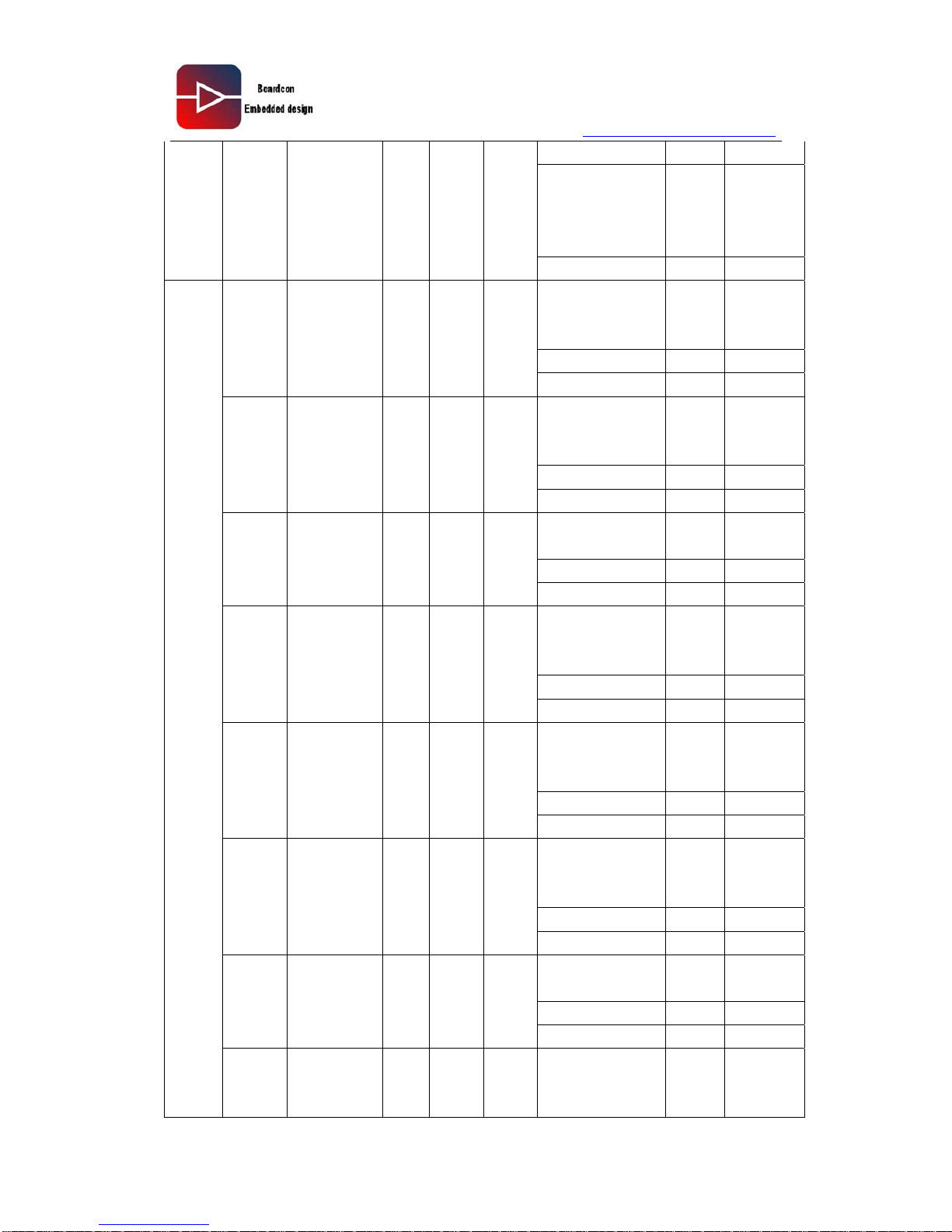
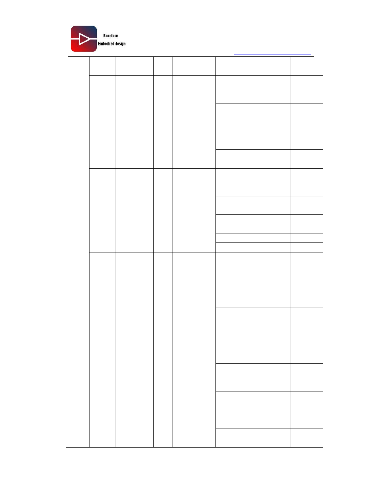
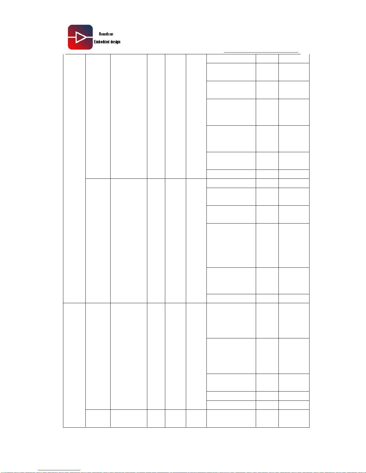
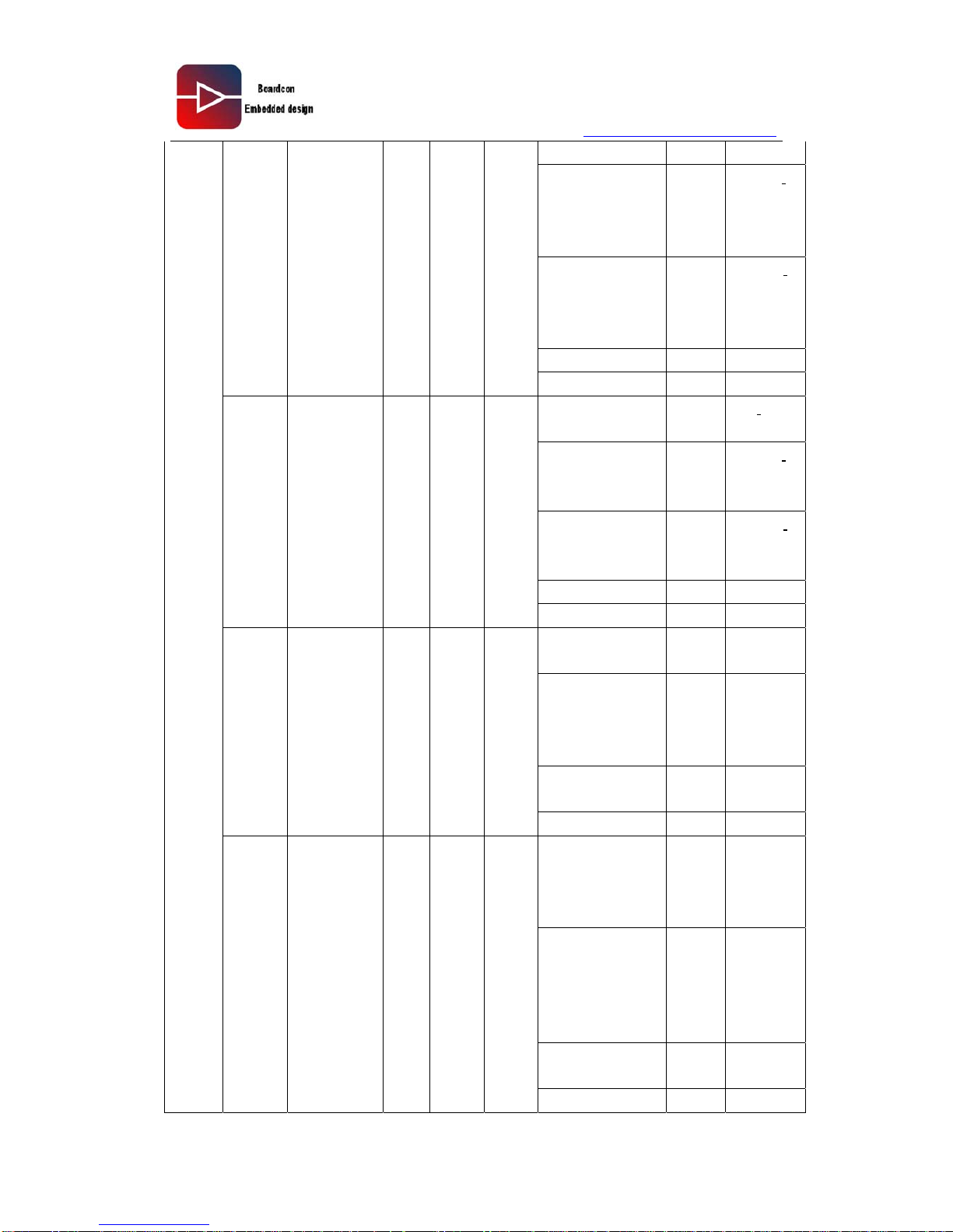
2.2.5 Pin Signal Careful Introduction
Function
Module
board
pins
Pin
description
IO
initial
state
IO
categ
ory
Worki
ng
voltag
e
Pins remultiplexing
function
Input
and
output
Function
description
1—3 VDD_5V I P 5 VDD_5V I 5V
4—5 VDD_IO I P 3.3 VDD_IO I IO
6 VDD_ARM O P
1.2/1.
3
VDD_ARM O ARM
7 VDD_INT O P
1.2/1.
3
VDD_INT O INT
8
VDD_MDD
R
O P 1.8 VDD_MDDR O Memory
9 VDD_RTC I P 3 VDD_RTC I RTC
power
10 GND \ P \ GND \
地
control 11
PWRRGTO
N
O(L) hag
1.8-3.
3
PWRRGTON O
Core
voltage
control
pin
ADDR18 O
Bus
address
GPQ0 IO GPIO
GPIO 12 GPQ0
O(H
)
hbg
1.8-3.
3
EINT9[0] I interrupt
13 OTGID AI hr
1.8-3.
3
OTGID I USB ID
14 OTGDP AI htr
1.8-3.
3
OTGDP IO
USB
Differenti
al data
(+)
15 OTGDM AI htr
1.8-3.
3
OTGDM IO
USB
Differenti
al data(-)
16 VBUS AI htr
1.8-3.
3
VBUS IO
USB BUS
power
17
OTGDRV_
VBUS
O(L) hag
1.8-3.
3
USBDRVVBUS O
OTGpow
er supply
control
pin
USB
18 USBDP AI usb1 \ uhDP IO USB
Page 16
www.armdesigner.com
Android6410 Reference Guide
16
HOST
DGPS
(+)
19 USBDN AI usb1 \ uhDN IO
USB
HOST
DGPS(-)
GPC[6] IO GPIO
spiMOSI[1] IO
SPI1 Out
from the
main
entry
20 SPIMOSI1 I hag
1.8-3.
3
EINT2[6] I interrupt
GPC[7] IO GPIO
spiCS[1] IO
SPI1
Chip
select
I2SMULTI_DO[2] O I2S SDO
SPI
21 SPICS1 I hag
1.8-3.
3
EINT2[7] I interrupt
GPG[2:5] IO GPIO
mmcDAT0[0:3] IO
MMC
data
22—25
SD0_DATA
[0:3]
I hag
1.8-3.
3
EINT5[2:5] I interrupt
GPG[0] IO GPIO
mmcCLK0 O
MMC
clock
26 SD0_CLK I hag
1.8-3.
3
EINT5[0] I interrupt
GPG[1] IO GPIO
mmcCMD0 IO
MMC
CMD
27 SD0_CMD I hag
1.8-3.
3
EINT5[1] I interrupt
GPG[6] IO GPIO
mmcCDN0 I
MMC
card
query
mmcCDN1 I
MMC
card
query
28 SD0_CDn I hag
1.8-3.
3
EINT5[6] I Interrupt
GPL[13] IO GPIO
hiDATA[16] IO HSI data
EINT[21] I Interrupt
SDIO
29 SD0_WPn I hag
1.8-3.
3
DATA_CF[8] IO CF card
Page 17
www.armdesigner.com
Android6410 Reference Guide
17
data
GPH[2:5] IO GPIO
mmcDAT1[0:3] IO
MMC
data
kpCOL[2:5] O
Column
code
30—33
SD1_DATA
[0:3]
I hag
1.8-3.
3
EINT6[2:5] I interrupt
GPH[0] IO GPIO
mmcCLK1 IO
MMC
clock
kpCOL[0] O
Keyboard
Column
code
34 SD1_CLK I hag
1.8-3.
3
EINT6[0] I Interrupt
GPH[1] IO GPIO
mmcCMD1 IO
MMC
CMD
kpCOL[1] O
Keyboard
Column
code
35 SD1_CMD I hag
1.8-3.
3
EINT6[1] I Interrupt
GPN[6] IO GPIO
EINT[6] I Interrupt
36 SD1_CDn I hag
1.8-3.
3
kpROW[6] I
Keyboard
line code
GPL[14] IO GPIO
hiDATA[17] IO
HSI
address
EINT[22] I interrupt
37 SD1_WPn I hag
1.8-3.
3
DATA_CF[9] IO
CF card
data
GPE[0] IO GPIO
pcmDCLK[1] O
PCM
Serial
conversio
n clock
i2sCLK[1] IO I2S clock
38 GPE0 I hag
1.8-3.
3
97BITCLK I
AC97-bit
data
transfer
clock
GPIO
39 GPE1 I hag 1.8-3. GPE[1] IO GPIO
Page 18
www.armdesigner.com
Android6410 Reference Guide
18
pcmEXTCLK[1] I
PCM
clock
selection
i2sCDCLK[1] O
I2S
CODEC
system
clock
3
97RESETn O
AC97
reset
signal
GPE[2] IO GPIO
pcmFSYNC[1] O
PCM
data
transfer
start flag
word
i2sLRCK[1] IO
I2S
channel
selection
clock
40 GPE2 I hag
1.8-3.
3
97SYNC O
AC97
field sync
signal
GND 41—50 GND \ P \ GND \ GND
ADC 51—52 ADCIN [0:1] AI hr
1.8-3.
3
ADC_AIN[0:1] AI
AD
conversio
n analog
input
Test 53 nBATF I hag
1.8-3.
3
nBATF I
Battery
fault
indication
Reset 54 KEY_RST I hag 3.3 KEY_RST I
Outside
reset
signal
input
GPH[9] IO GPIO
mmcDAT1[7] IO
MMC
data
mmcDAT2[3] IO
MMC
data
GPIO 55 GPH9 I hag 1.8-3.
3
I2SMULTI_DI I
I2S data
input
Page 19
www.armdesigner.com
Android6410 Reference Guide
19
EINT6[9] I Interrupt
GPN0 IO GPIO
EINT0 I Interrupt
56 EINT0 I
hag_a 1.8-3.
3
KPROW0 I
keyboard
line code
GPN2 IO GPIO
EINT2 I Interrupt
interrupt
57 EINT2 I
hag_a 1.8-3.
3
KPROW2 I
keyboard
line code
Start
set
58—61 OM[1:4] I hag
1.8-3.
3
OM[1:4] I
Operatio
n mode
selection
GPH[6] IO GPIO
mmcDAT1[4] IO
MMC
data
mmcDAT2[0] IO
MMC
data
kpCOL[6] O
keyboard
line code
I2SMULTI_SCLK IO
I2S bus
clock
ADDR_CF[0] O
CF card
address
GPIO 62 GPH6 I hag
1.8-3.
3
EINT6[6] I Interrupt
reset 63 NREST O hag
1.8-3.
3
NREST O
System
reset
output
64 ADDR2 O(L) hbg
1.8-3.
3
ADDR2 O
memory
0 address
bus
GPN[7] IO GPIO
EINT[7] I Interrupt
65 IRQ_LAN I
hag_a 1.8-3.
3
kpROW[7] I
Keyboard
scan
code
66 CSn1
O(H
)
hbg
1.8-3.
3
nCS O
Select
Memory
0
nWE O
Memory
Write
Enable 0
Bus
67 WEn
O(H
)
hbg
1.8-3.
3
nIOWR_CF O Memory
Page 20
www.armdesigner.com
Android6410 Reference Guide
20
0 write
enable
under IO
mode
nOE O
Memory
0 output
enable
68 OEn
O(H
)
hbg
1.8-3.
3
nIORD_CF O
Memory
0 read
enable
under IO
mode
69—84 DATA [0:15] I hbg
1.8-3.
3
DATA [0:15] O
Memory
0 data
bus
GPB[5] I GPIO
i2cSCL[0] IO I2C clock
85 I2CSCL0 I hag
1.8-3.
3
EINT1[13] I Interrupt
GPB[6] I GPIO
i2cSDA[0] IO I2C data
I2C
86 I2CSDA0 I hag
1.8-3.
3
EINT1[14] I Interrupt
CAMRSTn I
Cameras
soft clear
signal
GPF5 IO GPIO
87 CAMRSTn I hag
1.8-3.
3
EINT4[5] I Interrupt
CAMHREF I
Cameras
horizontal
synchroni
zation
GPF8 IO GPIO
88 CAMHREF I hag
1.8-3.
3
EINT4[8] I Interrupt
CAMVSYNC I
Camera
field
synchroni
zation
GPF7 IO GPIO
89
CAMVSYN
C
I hag
1.8-3.
3
EINT4[7] I Interrupt
CAMCLK I
Camera
mclk
GPF9 IO GPIO
Camera
90 CAMCLK I hag
1.8-3.
3
EINT4[9] I interrupt
Page 21
www.armdesigner.com
Android6410 Reference Guide
21
CAMPCLK I
Camera
PCLK
GPF6 IO GPIO
91 CAMPCLK I hag
1.8-3.
3
EINT4[6] I Interrupt
CAMDATA[0:7] I
Camera
data
GPF[5:12] IO GPIO
92—99
CAMYDAT
A [0:7]
I hag
1.8-3.
3
EINT4[5:12] I Interrupt
GPN4 IO GPIO
EINT4 I Interrupt
100 EINT4 I
hag_a 1.8-3.
3
KPROW4 I
Keyboard
line code
GPN9 IO GPIO
101 EINT9 I
hag_a 1.8-3.
3
EINT9 I Interrupt
GPN12 IO GPIO
102 EINT12 I
hag_a 1.8-3.
3
EINT12 I Interrupt
GPN1 IO GPIO
EINT1 I Interrupt
103 EINT1 I
hag_a 1.8-3.
3
KPROW1 I
Keyboard
line code
GPN3 IO GPIO
EINT4 I Interrupt
104 EINT3 I
hag_a 1.8-3.
3
KPROW3 I
Keyboard
line code
GPN5 IO GPIO
EINT5 I Interrupt
interrupt
105 EINT5 I
hag_a 1.8-3.
3
KPROW5 I
Keyboard
line code
GPC[3] IO GPIO
spiCS[0] IO
SPI0 chip
selection
106 SPICS0 I hag
1.8-3.
3
EINT2[3] I Interrupt
GPC[1] IO GPIO
spiCLK[0] IO
SPI0
clock
107 SPICLK0 I hag
1.8-3.
3
EINT2[1] I Interrupt
GPC[0] IO GPIO
spiMISO[0] IO
SPI0
must in
slave
output
SPI
108 SPIMISO0 I hag
1.8-3.
3
EINT2[0] I Interrupt
Page 22
www.armdesigner.com
Android6410 Reference Guide
22
GPC[2] IO GPIO
spiMOSI[0] IO
SPI0
must
output
slave in
109 SPIMOSI0 I hag
1.8-3.
3
EINT2[2] I Interrupt
RXD[0] I
UART 0
receive
data input
EINT1[0] I Interrupt
110 RXD0 I hag
1.8-3.
3
GPA[0] IO GPIO
TXD[0] O
UART 0
send data
input
EINT1[1] I interrupt
111 TXD0 I hag
1.8-3.
3
GPA[1] IO GPIO
CTSn[0] I
UART 0
CTSn
EINT1[2] I Interrupt
112 CTSN0 I hag
1.8-3.
3
GPA[2] IO GPIO
RTSn[0] O
UART 0
send data
inquiry
EINT1[3] I Interrupt
113 RTSN0 I hag
1.8-3.
3
GPA[3] IO GPIO
RXD[1] I
UART 1
receive
data input
EINT1[4] I Interrupt
114 RXD1 I hag
1.8-3.
3
GPA[4] IO GPIO
TXD[1] O
UART 1
send data
output
EINT1[5] I Interrupt
115 TXD1 I hag
1.8-3.
3
GPA[5] IO GPIO
CTSn[1] I
UART 1
CTSn
EINT1[6] I Interrupt
116 CTSN1 I hag
1.8-3.
3
GPA[6] IO GPIO
UART
117 RTSN1 I hag
1.8-3.
3
RTSn[1] O
UART 1
send data
inquiry
Page 23
www.armdesigner.com
Android6410 Reference Guide
23
EINT1[7] I Interrupt
GPA[7] IO GPIO
RXD[2] I
UART 2
receive
data input
irRXD I
Infrared
data
received
ADDR_CF[0] O
CF card
address
EINT1[8] I Interrupt
118 RXD2 I hag
1.8-3.
3
GPB[0] IO GPIO
TXD[2] O
UART 2
send data
output
irTXD O
Infrared
data send
ADDR_CF[1] O
CF card
address
EINT1[9] I Interrupt
119 TXD2 I hag
1.8-3.
3
GPB[1] IO GPIO
RXD[3] I
UART 3
data
received
irRXD I
Infrared
data
received
ADDR_CF[2] O
CF card
address
i2cSCL[1] IO
I2C clock
line
EINT1[10] I
interrupt
120 RXD3 I hag
1.8-3.
3
GPB[2] IO GPIO
TXD[3] O
UART 3
data send
irTXD O
Infrared
data send
i2cSDA[1] IO
I2C data
line
EINT1[11] I Interrupt
121 TXD3 I hag
1.8-3.
3
GPB[3] IO GPIO
Page 24
www.armdesigner.com
Android6410 Reference Guide
24
GPH[7] IO GPIO
mmcDAT1[5] IO
MMC
data
mmcDAT2[1] IO
MMC
data
kpCOL[7] O
Keyboard
column
codes
I2SMULTI_CDC
LK
IO
I2S
CODEC
clock
ADDR_CF[1] O
CF card
address
122 GPH7 I hag
1.8-3.
3
EINT6[7] I Interrupt
GPH[8] IO GPIO
mmcDAT1[6] IO
MMC
data
mmcDAT2[2] IO
MMC
data
I2SMULTI_LRCL
K
IO
I2S clock
switching
left and
right
channels
ADDR_CF[2] O
CF 卡
card
address
GPIO
123 GPH8 I hag
1.8-3.
3
EINT6[8] I Interrupt
I2SCDCLK[0] O
I2S
codec
system
clock
pcmEXTCLK[0] I
Optional
clock
input
PCM
AC97_RSTN O
AC97res
et signal
EINT3[1] I Interrupt
124
AC97_RST
N
I hag
1.8-3.
3
GPD[1] IO GPIO
Audio
125 AC97_SDO I hag
1.8-3.
3 I2SDO O I2S serial
data
Page 25
www.armdesigner.com
Android6410 Reference Guide
25
output
pcmSOUT[0] O
PCM
serial
data
output
AC97_SDO O
AC97
serial
data
output
EINT3[4] I Interrupt
GPD[4] IO GPIO
I2SDI[0] I
I2S
serial
data input
pcmSIN[0] I
PCM
serial
data input
AC97_SDI I
AC97
serial
data input
EINT3[3] I Interrupt
126 AC97_SDI I hag
1.8-3.
3
GPD[3] IO GPIO
I2SCLK[1] IO
I2S Serial
Clock
pcmDCLK[1] O
PCM
serial
conversio
n clock
AC97_BITCLK I
AC97 Bit
Clock
127
AC97_
BITCLK
I hag
1.8-3.
3
GPE[0] IO GPIO
I2SLRCK[0] IO
I2S left
channel
select
clock
pcmFSYNC[0] O
PCM
word
synchroni
zation
flag
AC97_SYNC O
AC97
sync
128
AC97_SYN
C
I hag
1.8-3.
3
EINT3[2] I interrupt
Page 26
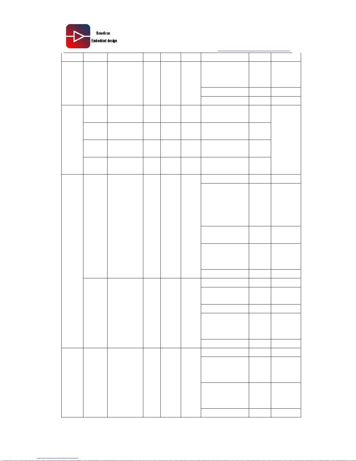
www.armdesigner.com
Android6410 Reference Guide
26
GPD[2] IO GPIO
Xm0CSn[4:5] O
Select
Memory
0
GPO[2:3] IO GPIO
GPIO
129-13
0
GPO[2:3]
O(H
)
hbg
1.8-3.
3
EINT7[2:3] I Interrupt
131 TSXM AI hr
1.8-3.
3
adc_AIN6 AI
132 TSXP AI hr
1.8-3.
3
adc_AIN7 AI
133 TSYM AI hr
1.8-3.
3
adc_AIN4 AI
touch
134 TSYP AI hr
1.8-3.
3
adc_AIN5 AI
ADC data
input
GPC[4] IO GPIO
spiMISO[1] IO
SPI1
must
input
slave
output
mmcCMD2 IO
MMC
order
I2SMULTI_DO[0] O
I2S serial
data
output
135 SPIMISO1 I hag
1.8-3.
3
EINT2[4] I Interrupt
GPC[5] IO GPIO
spiCLK[1] IO
SPI1
clock
mmcCLK2 O MMC clck
I2SMULTI_DO[1] O
I2S serial
data
output
SPI
136 SPICLK1 I hag
1.8-3.
3
EINT2[5] I interrupt
GPL[0:2] IO GPIO
hiADDR[0:2] I
HSI
address
line
kpCOL[0:2] O
Keyboard
column
codes
Matrix
Keyboar
d
137—1
39
KP_COL
[0:2]
I hag
1.8-3.
3
ADDR_CF[0:2] O CF
Page 27
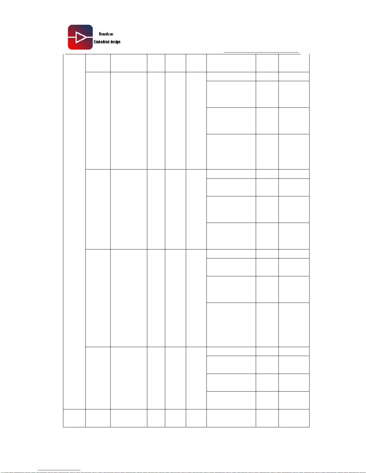
www.armdesigner.com
Android6410 Reference Guide
27
address
line
GPL[3] IO GPIO
hiADDR[3] I
HSI
address
line
kpCOL[3] O
Keyboard
column
codes
140 KP_COL3 I hag
1.8-3.
3
m0INTata I
Interrupt
request in
memory
0
GPL[4] IO GPIO
hiADDR[4] I
HIS
address
kpCOL[4] O
Keyboard
column
codes
141 KP_COL4 I
hag_a 1.8-3.
3
m0RESETata I
Memory
0 reset
signal
GPL[5] IO GPIO
hiADDR[5] I
HIS
address
kpCOL[5] O
Keyboard
column
codes
142 KP_COL5 I
hag_a 1.8-3.
3
m0INPACKata O
Memory
0 input
Configure
d as IO
mode
GPK[8:13] IO GPIO
hiDATA[8:13] IO
HIS Data
line
kpROW[0:5] I
Keyboard
row code
143—1
48
KP_ROW
[0:5]
I
hag_a 1.8-3.
3
DATA_CF[8:13] IO
CFcard
data line
LCD
149—1
56
VD[0:7] I
hag_a 1.8-3.
3 VD[7:0] O RGB
Interface
Page 28
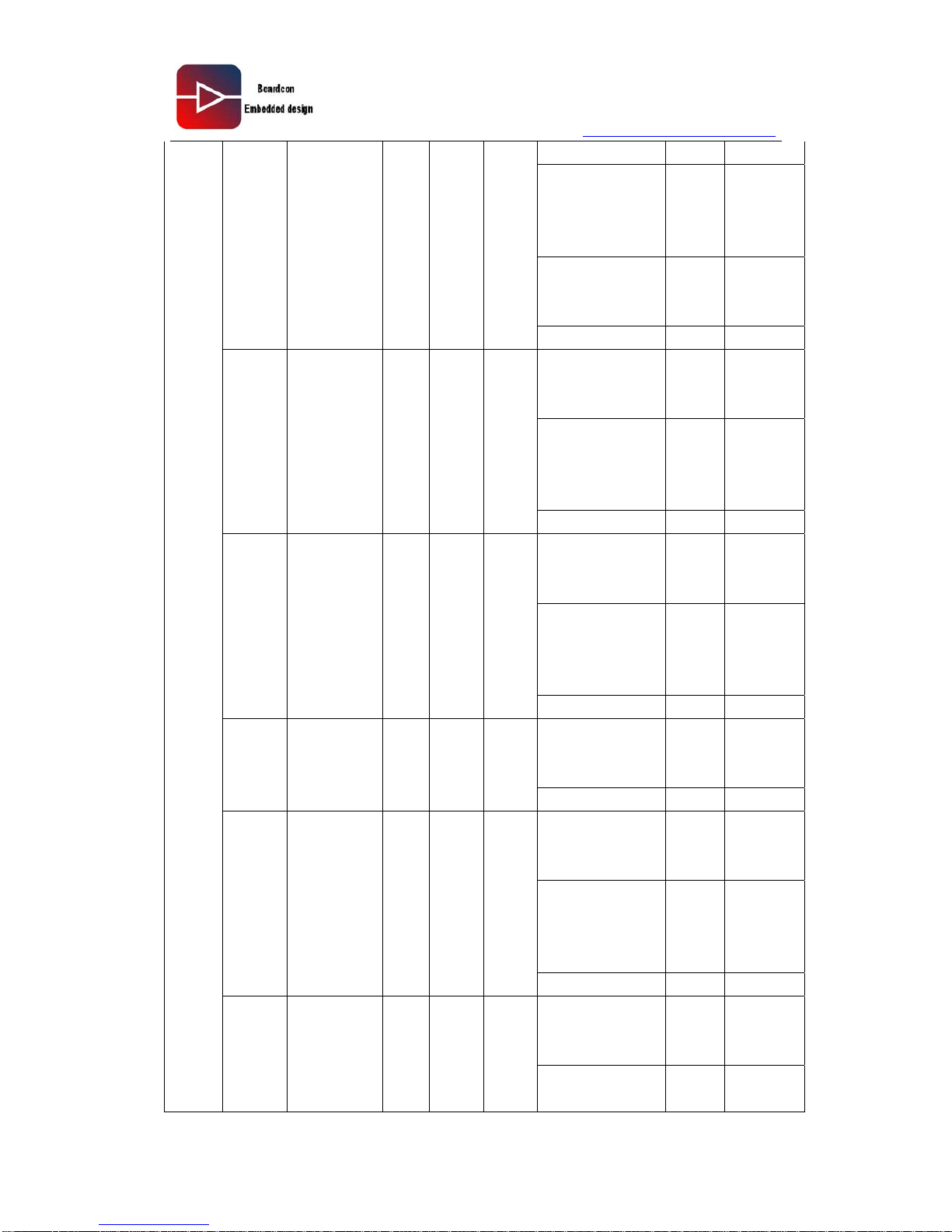
www.armdesigner.com
Android6410 Reference Guide
28
Data bit
SYS_VD[7:0] IO
i80
system
interface
data bits
VEN_DATA[7:0] O
601
Interface
Data bit
GPI[7:0] IO GPIO
VD[15:8] O
RGB
Interface
Data bit
SYS_VD[15:8] IO
i80
system
interface
data bits
157—1
64
VD[8:15] I
hag_a 1.8-3.
3
GPI[15:8] IO GPIO
VD[17:16] O
RGB
Interface
Data bit
SYS_VD[17:16] IO
i80
system
interface
data bits
165—1
66
VD[16:17] I
hag_a 1.8-3.
3
GPJ[1:0] IO GPIO
VD[21:18] O
RGB
Interface
Data bit
167—1
70
VD[18:21] I
hag_a 1.8-3.
3
GPJ[5:2] IO GPIO
VD[22] O
RGB
Interface
Data bit
SYS_VSYNC_L
DI
O
I80 field
synchron
ous
signal bit
171 VD[22] I
hag_a 1.8-3.
3
GPJ[6] IO GPIO
VD[23] O
RGB
Interface
Data bit
172 VD[23] I
hag_a 1.8-3.
3
SYS_OEn O I80
Output
Page 29
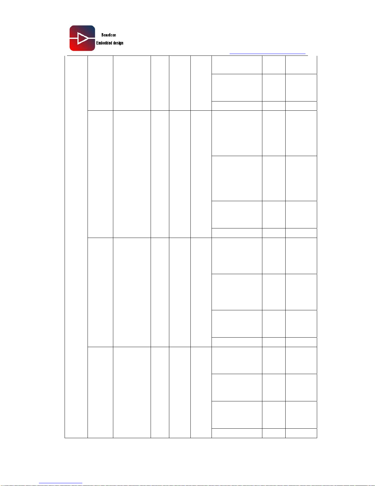
www.armdesigner.com
Android6410 Reference Guide
29
Enable
bit
VEN_FIELD O
Interface
601 bit
sync field
GPJ[7] IO GPIO
VSYNC O
RGB
vertical
synchroni
zation
signals
SYS_CSn_sub O
i80
second
chip
select
signal
VEN_VSYNC O
601 field
sync
signal
173 VSYNC I
hag_a 1.8-3.
3
GPJ[9] IO GPIO
HSYNC O
RGB
sync
signal
line
SYS_CSn_main O
i80 main
chip
select
signal
VEN_HSYNC O
601 line
sync
signal
174 HSYNC I
hag_a 1.8-3.
3
GPJ[8] IO GPIO
VCLK O
GGB dot
clock
signal
SYS_Wen O
i80 write
enable
signal
601_CLK O
601 data
transfer
clock
175 VCLK I
hag_a 1.8-3.
3
GPJ[11] IO GPIO
Page 30
www.armdesigner.com
Android6410 Reference Guide
30
VDEN O
RGB data
enable
signal
SYS_RS O
i80
register /
status
signal
control bit
VEN_HREF O
601 data
enable
signal
176 VDEN I
hag_a 1.8-3.
3
GPJ[10] IO GPIO
GPF[15] IO GPIO
PWM 177
PWM_TOU
T1
I hag
1.8-3.
3
pwmTOUT[1] O
PWM
output
GPE[3] IO GPIO
pcmSIN[1] I
PSM
serial
data input
i2sDI[1] I
I2S serial
data input
178 GPE3 I hag
1.8-3.
3
97SDI I
AC97
serial
data input
GPE[4] IO GPIO
pcmSOUT[1] O
PCM
serial
data
output
i2sDO[1] O
I2S serial
data
output
GPIO
179 GPE4 I hag
1.8-3.
3
97SDO O
AC97
serial
data
output
DAC 180 DAC_OUT0 AO hr
1.8-3.
3
dacOUT_0 AO
DAC
analog
output
IO Type Definition:
hag: Wide range of 1.8 ~ 3.3V bi-directional buffer with Schmitt trigger input
Page 31
www.armdesigner.com
Android6410 Reference Guide
31
resistance can be configured up / down and A-type output driver
hag_a: Wide range of 1.8 ~ 3.3V bi-directional buffer with Schmitt trigger input
active, resistance can be configured up / down and A-type output driver
hbg: Wide range of 1.8 ~ 3.3V bi-directional buffer with Schmitt trigger input
resistance can be configured up / down and B-type output driver
drtc: 1.8 ~ 3.0V power supply for the RTC section
dth: 1.8 ~ 3.3V for the external logic-level
hr: 1.8V ~ 3.3V wide range of analog two-way path
htr: 1.8V ~ 3.3V tolerant wide range of analog two-way path
usb1: USB 1.1 pin
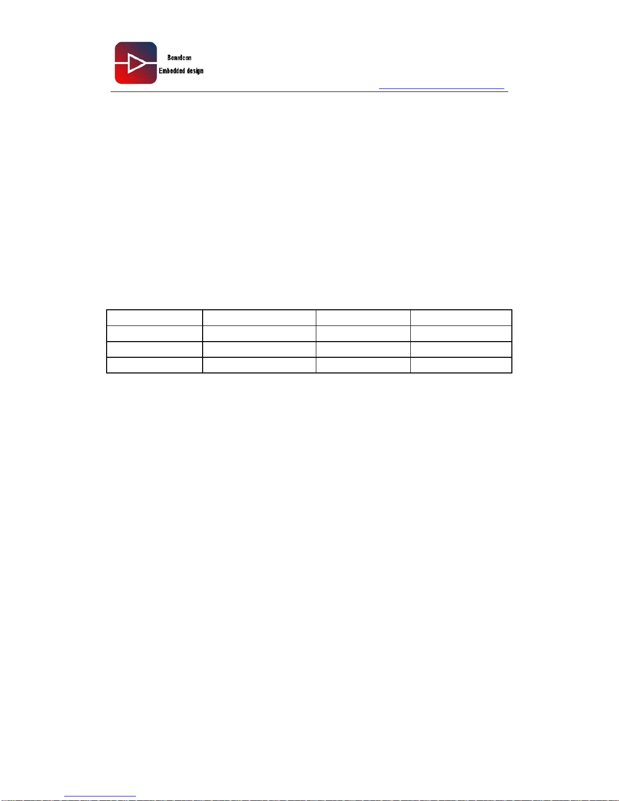
2.2.6 Core board input voltage / current shows
Number
Power Network
Voltage Electric current
1 VDD_5V 5V 100mA
2 VDD_IO 3.3V 60mA
3 VDD_RTC 3V 1mA
Page 32
www.armdesigner.com
Android6410 Reference Guide
32
2.3. Image of Carrier Board
Page 33
www.armdesigner.com
Android6410 Reference Guide
33
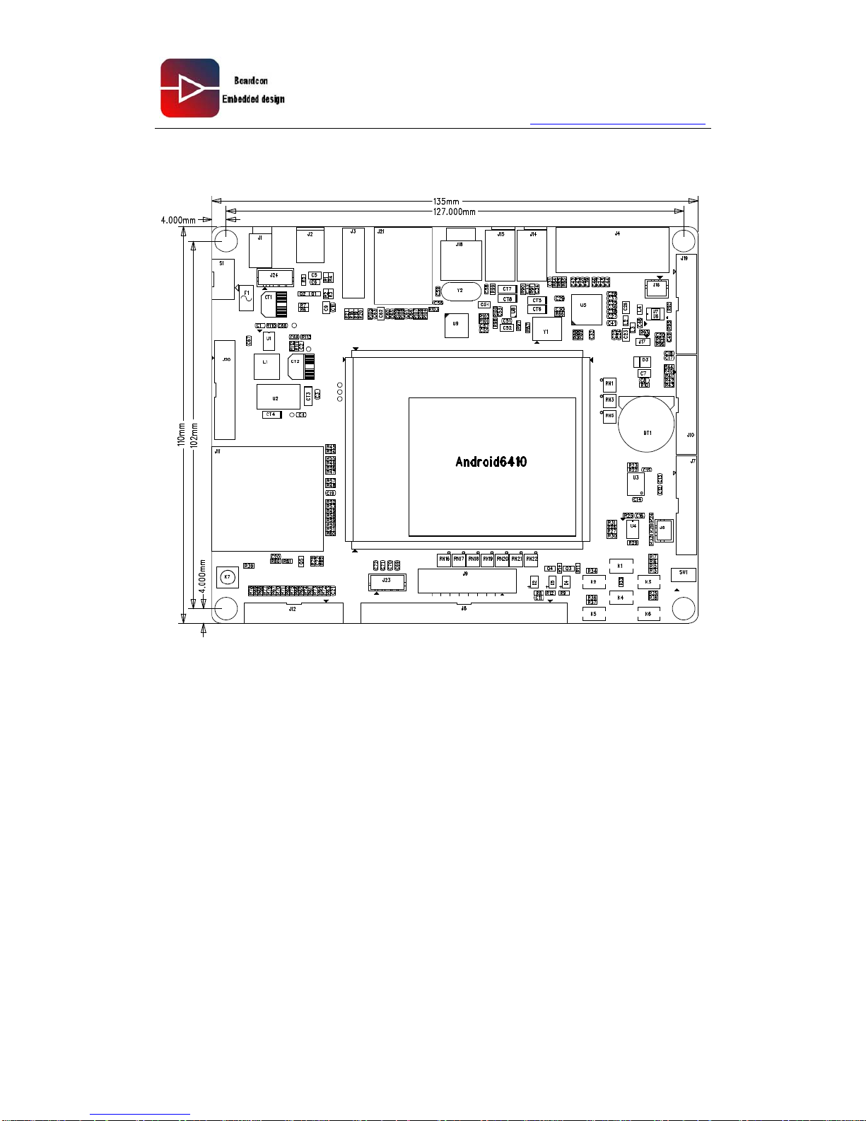
2.3.1 Carrier board structure and layout
3. Hardware design details
3.1. Power section
3.1.1. Power input interface
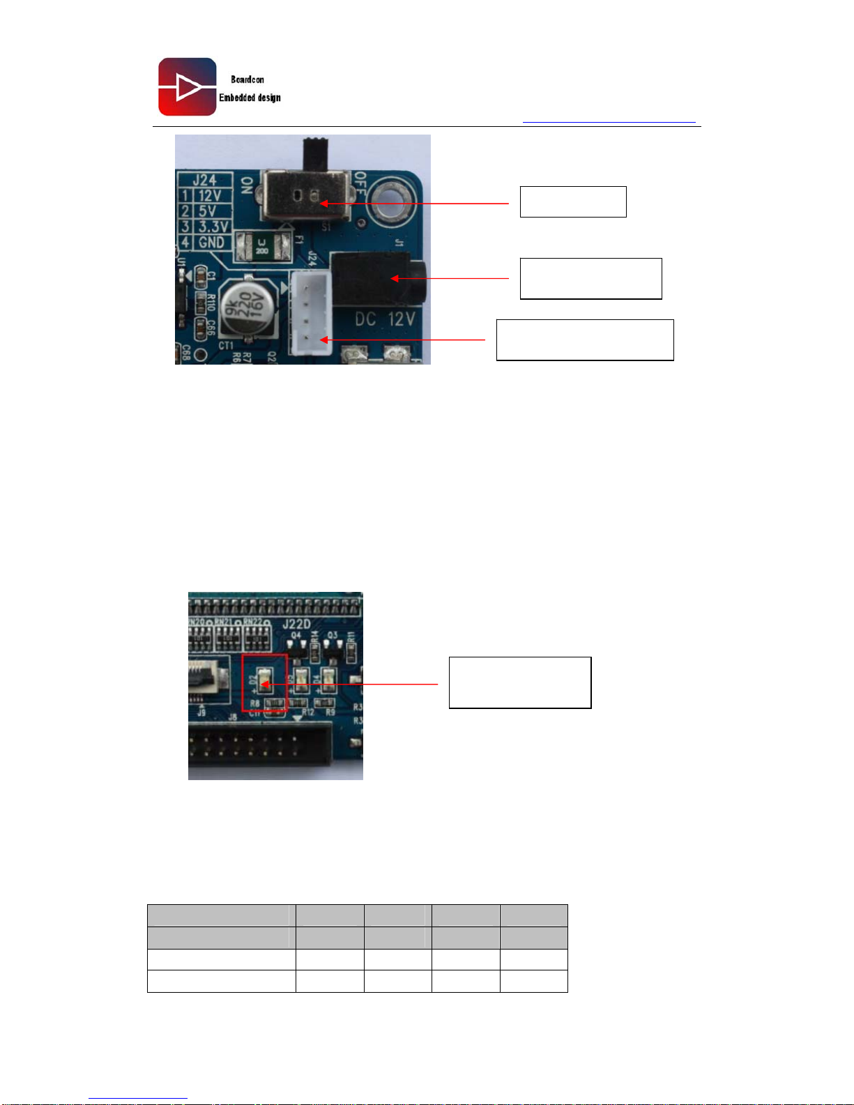
12V/2A power supply from the motherboard, use the power adapter to power outlet
through the mini DC_IN board power supply. We raises the power input interface to
facilitate users to connect an external DC power supply
Page 34
www.armdesigner.com
Android6410 Reference Guide
34
3.1.2 Power switch
Selected test-type power switch toggle switches for control of the board power supply ON
/ OFF.
3.1.3 Power LED
Red LED to indicate power status
3.2 Start setting
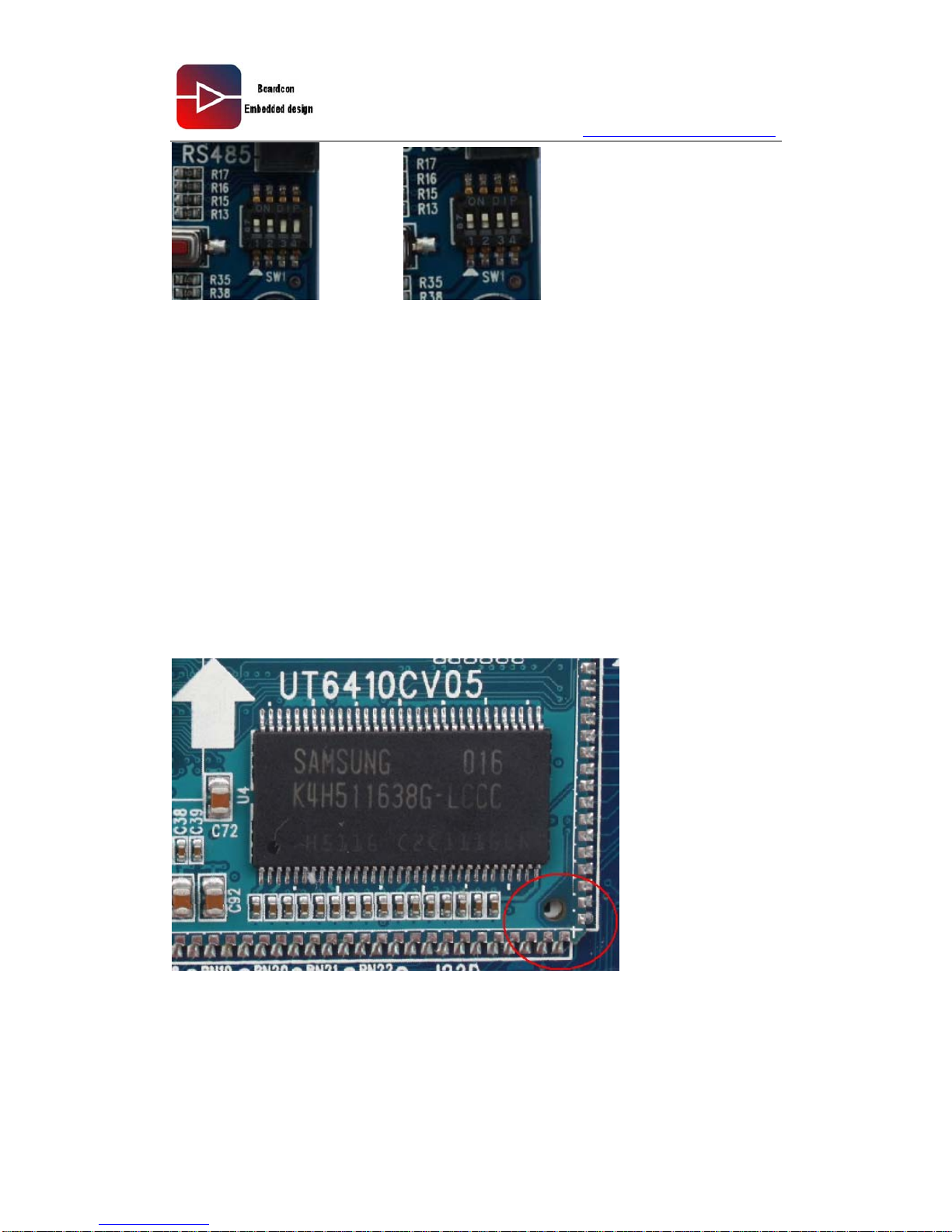
Android6410 supports two boot methods: SD card driver, Nand Flash start. By using four
DIP switch to set the OM signal to select the CPU boot mode.
Boot methods OM 1 OM2 OM3 OM4
SW1 DIP Switch Pin 1 2 3 4
SD card driver
1 1 1 1
Nand Flash start
1 1 0 0
Power switch
Power input interface
External DC power input
Power LED
Page 35
www.armdesigner.com
Android6410 Reference Guide
35
Nand Flash booting SD booting
Note:1. SW1 switch located in ON, it shows "1", located in OFF, it shows "0", "X" is high or
low
2. Android6410 Single board computer defaults setting for the NAND FLASH boot mode
3.3. Device Interface description
3.3.1. Module board interfaces
Android6410 is the stamp-hole interface, welding fixed, 184 pins. Stamp hole interface,
welding is more stable, more solid.
3.3.2 UART asynchronous serial port
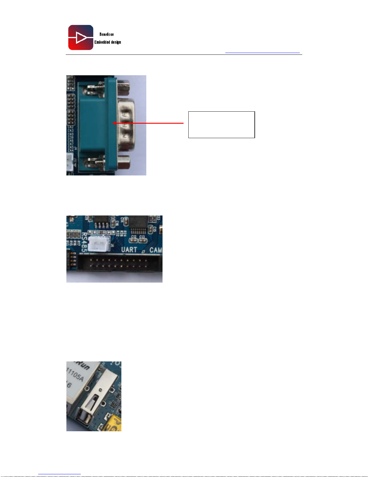
Android6410 Single Board Computer designed a total of 4-way serial port, serial port
supports RS232 and RS485.COM0 default setting for debugging serial port, via the serial
Page 36
www.armdesigner.com
Android6410 Reference Guide
36
cable is connected directly to PC, view the system debugging information.
COM1-COM3 serial port designed for applications which can be converted to RS485
serial port COM3 and used as it.
3.3.3 USB HOST interface
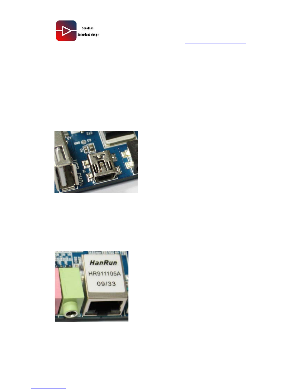
A USB HOST interface is compatible with OHCI Rev1.0, USB Rev1.1 agreement, with the
side plug type A USB Interface. Interface can connect U disc, USB mobile hard disk,
mouse, keyboard, 3G Modem, WIFI, Bluetooth and other USB devices.
COM0,debug
Page 37
www.armdesigner.com
Android6410 Reference Guide
37
3.3.4. USB OTG 2.0 Interface
OTG interface support USB2.0agreement, you can run at low speed (1.5Mbps, HOST
only), full speed (12Mbps, Device Only) and high-speed (480Mbps) mode. OTG interface,
when used as a USB Device, can be used to download programs, and computer sync to
transfer files, debug application procedures. Android6410 is on the use of Mini-A / B USB
socket, the default working in Device mode.
3.3.5. 100M Ethernet Interface
Android6410 Single Board Computer equips on-board 10/100M adaptive Ethernet port,
LAN chip DM9000 chip. Interfaces using a Link / Active LED and isolation transformer
RJ45 socket. Can be software set to automatically obtain IP via DHCP or static set IP.
Page 38
www.armdesigner.com
Android6410 Reference Guide
38
3.3.6. SD card Interface
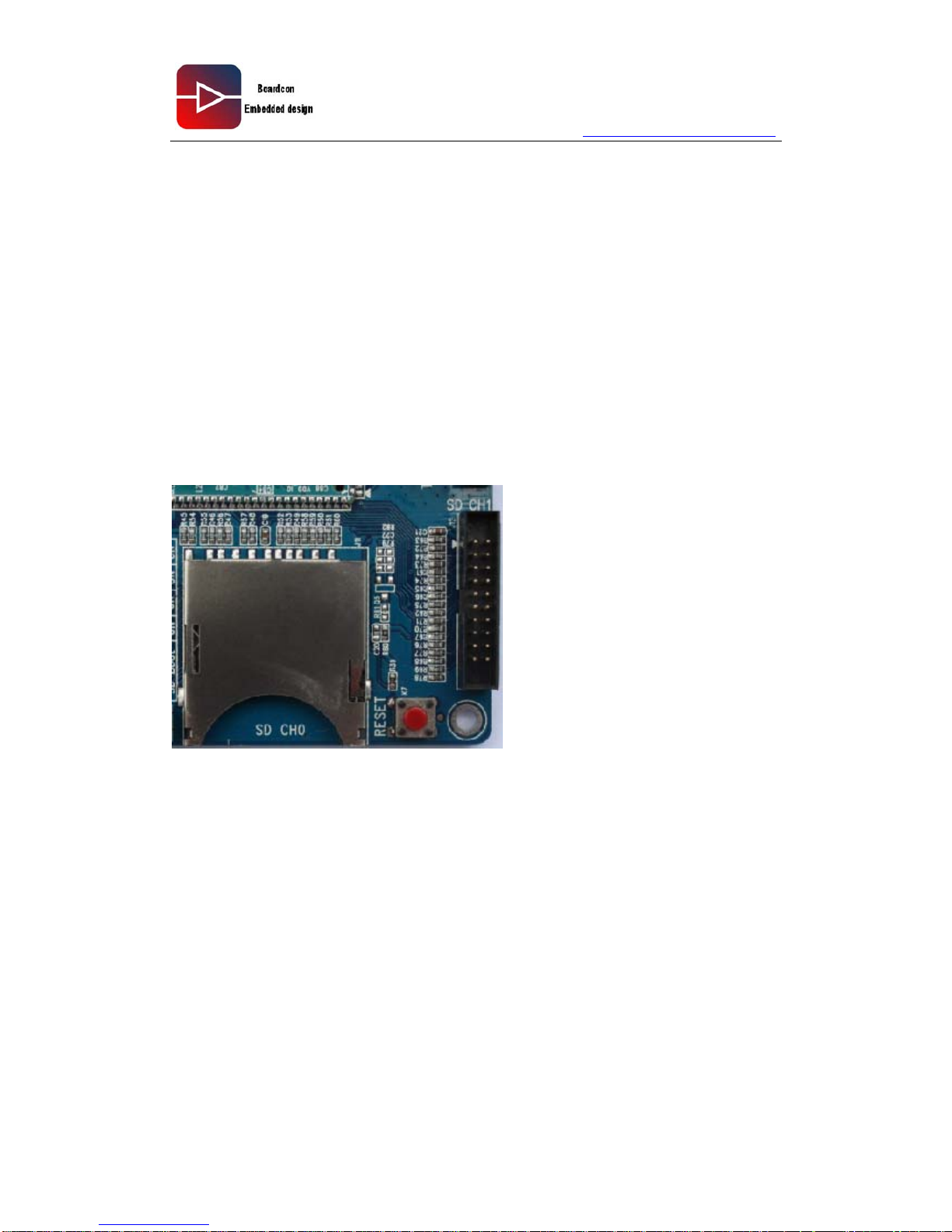
Android6410 Single Board Comptuer supports two channels of SD interfaces. One as a
standard SD slot, maximum support high-capacity SD card 32G Bytes. Compatible with
SD Host 2.0, SD Memory Card 2.0, SDIO Card 1.0 and High-Speed MMC 4.0, can be
used to access SD memory card, SDIO card and high-speed MMC card.
Another channel to 20pin pin leads SDIO, SDIO interfaces to facilitate users to connect
other devices, such as SDIO WIFI, DTV, etc..
Android6410 Single Board Computer support SD cards start, this feature can be achieved
with the fast USB OTG 2.0 firmware and system software upgrade. Completely replace
the traditional way JTAG programmer firmware, change means quick and easy. Suitable
for mass production
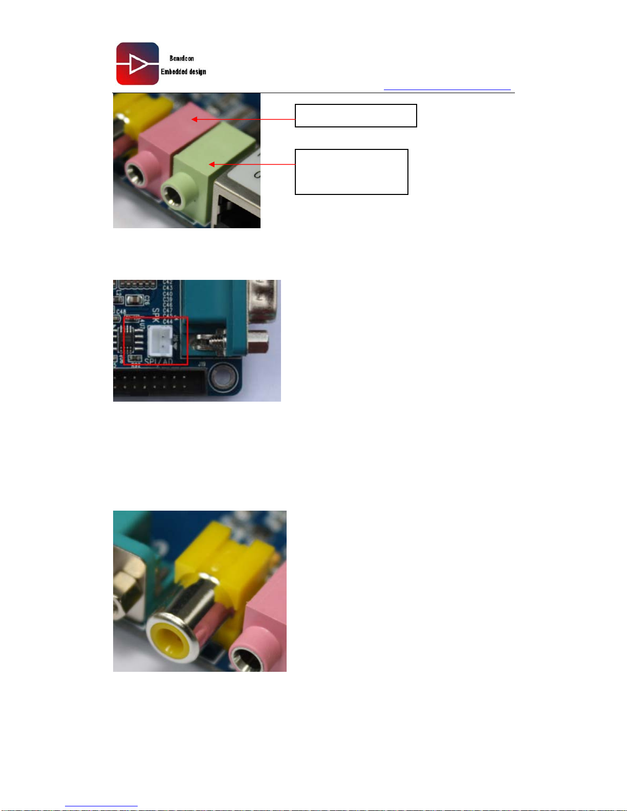
3.3.7. Audio Interface
Audio feature of Android6410 Single Board Computer 7 uses S3C6410 CPU and AC97
bus. Add WM9714 audio chip, to achieve integrated audio output and MIC input recording
function.
Audio input and output interfaces use 3.5 "audio jack
Page 39
www.armdesigner.com
Android6410 Reference Guide
39
Android6410 built-in amplifier, can be directly external speakers.
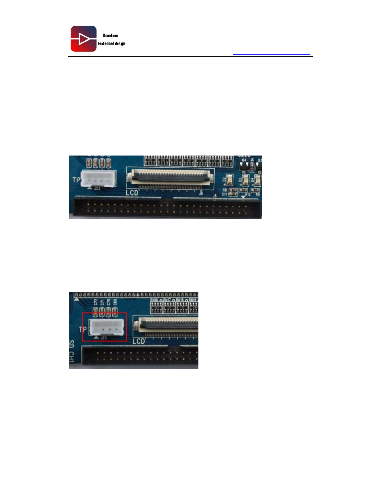
3.3.8. TV OUT Interface
Standard composite video signal output, can be directly connected to all kinds of video
playback equipment
MIC output interface
HEADPHONE output
interface
Page 40
www.armdesigner.com
Android6410 Reference Guide
40
3.3.9. LCD Interface
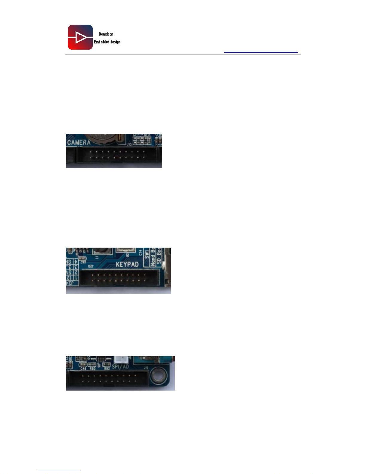
Android6410 Single Board Computer designed two LCD interfaces: one is 40pin FPC
interface, the other is double pin 2.0mm pitch 50pin interface, these interfaces are
included touch signal.
One FPC software interface is available through cable directly to the screen button on the
motherboard, and 50pin interface LCD module through the cable connection is also
convenient for users to debug their own flying line of LCD modules.
LCD interface signals to support 24BIT LCD, PWM backlight control, external interrupt
control
3.3.10. Four-wire resistive touch signal interface
To facilitate the user to debug the touch signal, touch signals alone leads to the 4pin
socket
3.3.11. CAMERA and IIC Interface
S3C6410 processor, camera support ITU-R BT 601/656 8-bit mode, the maximum you
can achieve 4096 × 4096 pixels.
Android6410 Single Board Computer to design a camera interface, using 10 × 2 pin
Page 41
www.armdesigner.com
Android6410 Reference Guide
41
Interface (J10). CAMERA interface in addition to the signal, but also increased the IIC
signal and a GPIO signal (CAM_PD/GPP14) most of the IIC Camera equipment needed
to configure the IIC so increasing the signal to facilitate the customers to connect the
camera directly to the use of equipment to prevent IIC CAMERA bus address conflicts
with other peripherals, Single Board Computer designed to replace the processor GPIO
IIC bus, on the CAMERA configuration.
UT_CAMERA_B, you can connect directly with Android6410 Single Board Computer use,
to achieve 1.3 million pixel camera features. Users may need to be matching
3.3.12. Matrix keyboard interface
Android6410 Single Board Computer raises of 6 * 6 matrix keyboard interface, enables
key functions of 36 independent and multi-function key combinations.
3.3.13. High speed SPI and AD Interface
Two high-speed SPI interface and the AD Interface
Page 42
www.armdesigner.com
Android6410 Reference Guide
42
3.3.14. User button
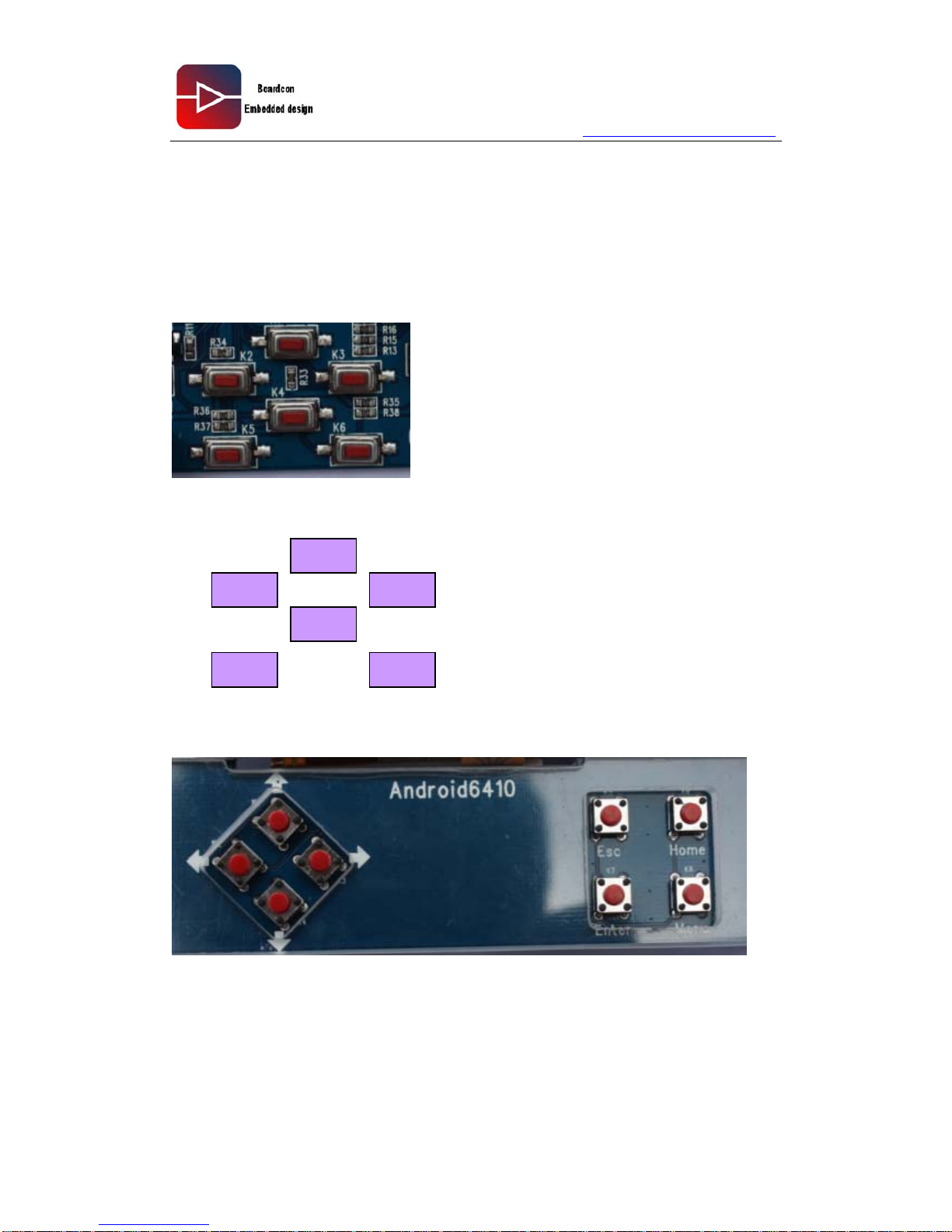
Android6410 Single Board Computer designs 6 key, key functions through GPIO interface.
Key support interrupt mode and query mode, function realization, down, left, right, OK, to
return. Users can control their own programming needs.
User button interface picture
The default function key definitions:
In addition to the keys on the floor, the Single Board Computer also adopted key matrix
keyboard interface module extended to LCD board, so that more user-friendly operations.
Implementation of functions: up, down, left, right, ESC, Home, Enter, menu, the main
function of these keys is the key function of the system with the android.
Left Right
UP
Down
Back Enter
Page 43
www.armdesigner.com
Android6410 Reference Guide
43
3.3.15 RTC
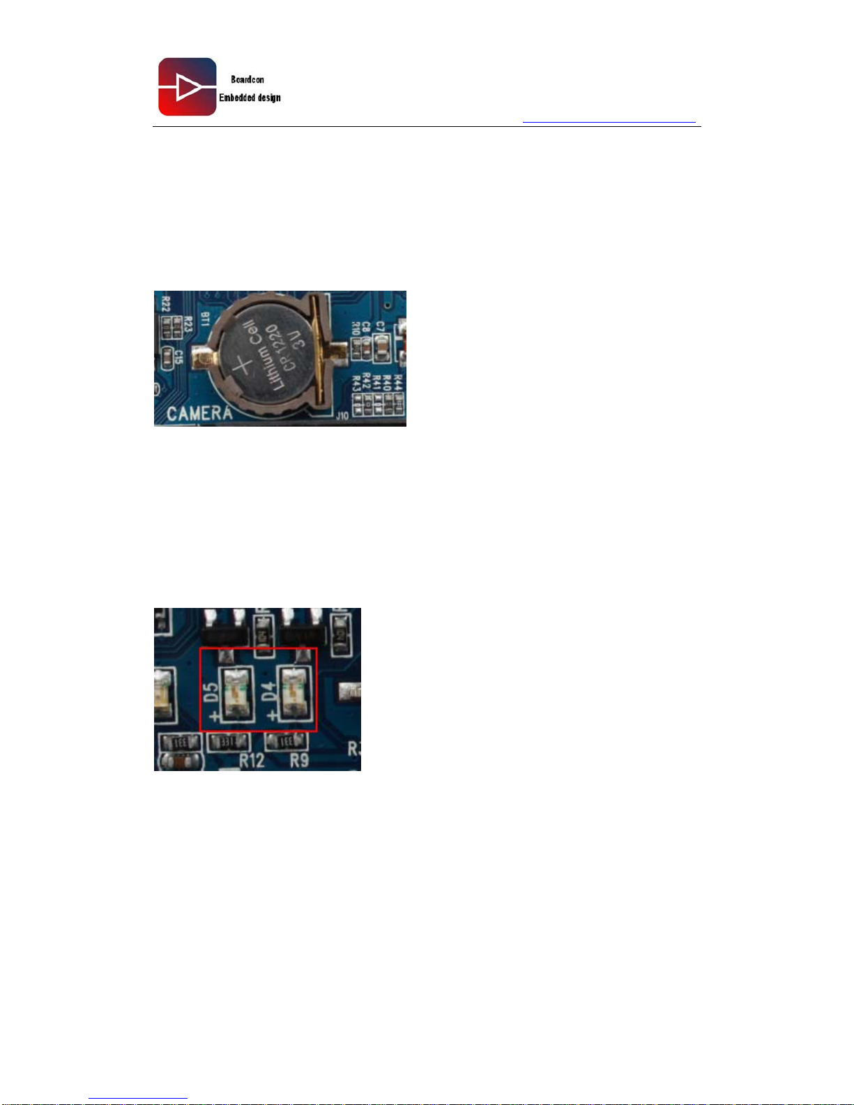
S3C6410 CPU is built-in RTC clock controller, without external RTC clock control chip.
Android6410 equipped with a CR1220 button battery models BT1, when the board
power-down, BT1 battery provide voltage, so that the RTC in CPU will continue to work;
when the board is in power, VDD3_IO will supply the RTC power.
3.3.16 LED User indicator
Android6410 configured two LED lights to indicate system operation, LED working status
of each LED connected via GPIO port to control.
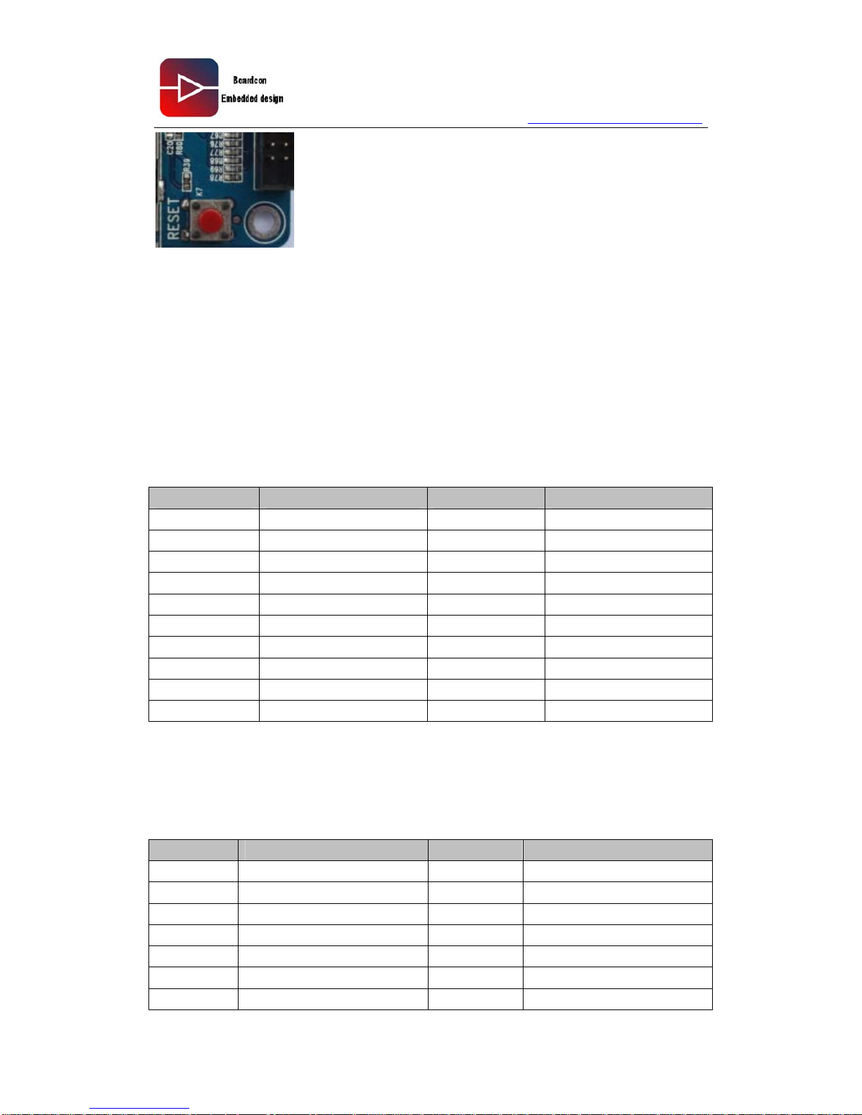
3.3.17 Reset Button
Android6410 system reset button using the 6 × 6 mm Tact switch, reset chip use
MAX811T. Reset chip to ensure system security, stability, state of the work.
Page 44
www.armdesigner.com
Android6410 Reference Guide
44
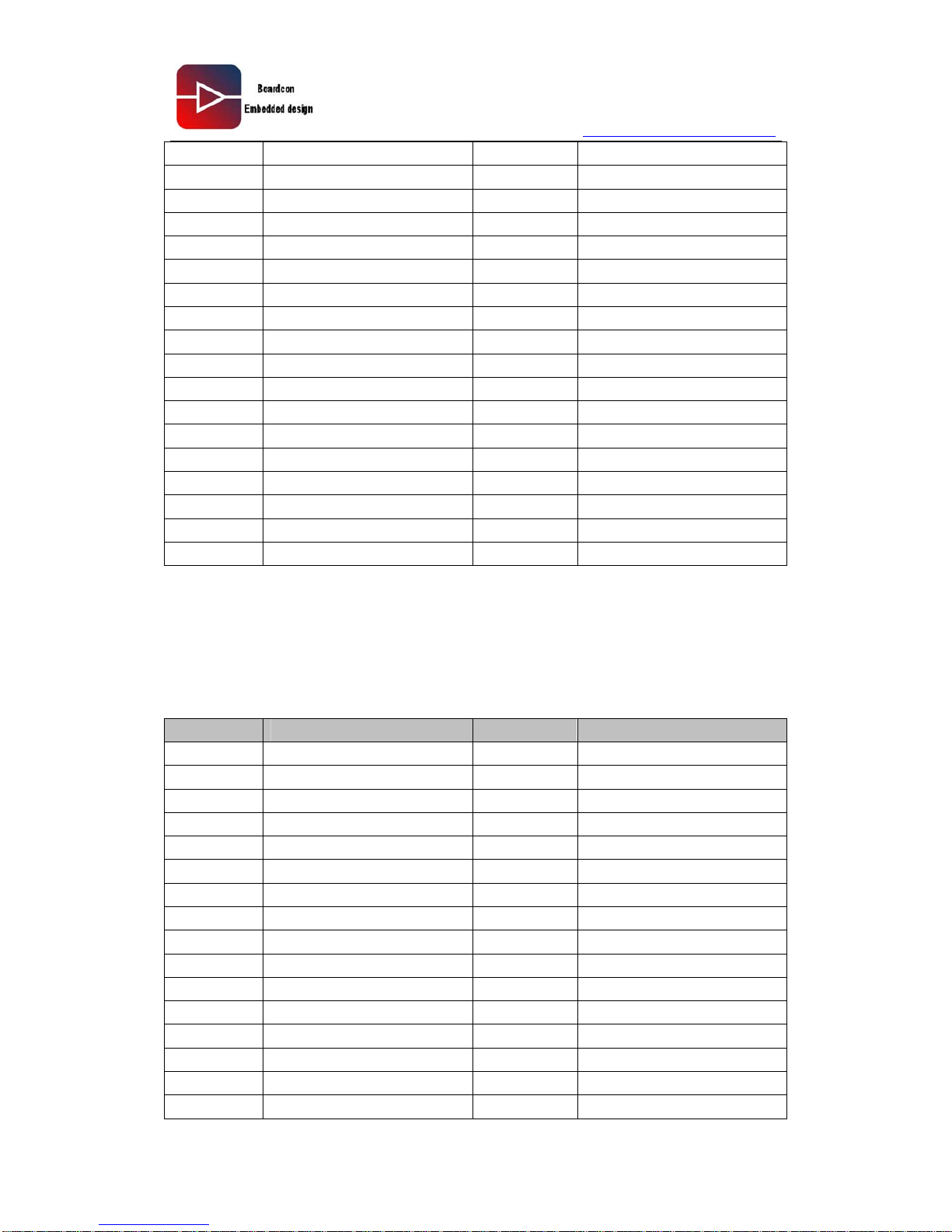
4. GPIO reserved
4.1. J7UART)
J7(UART)pin definition
Pin number Pin signal Pin number Pin signal
1
VDD_5V
11
TXD2
2
VDD_IO
12
RXD2
3
GPH8
13
TXD3
4
GPH9
14
RXD3
5
RTSn0
15
GPE0
6
CTSn0
16
GPE4
7
TXD1
17
GPQ0
8
RXD1
18
TXD1N
9
RTSn1
19
GND
10
CTSn1
20
RXD1N
4.2. J8(50PIN LCD)
J8(50PIN LCD)pin definition
Pin number Pin signal Pin number Pin signal
1
VDD_5V
26
LVD19
2
VDD_5V
27
LVD20
3
VDD_IO
28
LVD21
4
GND
29
LVD22
5
NC
30
LVD23
6
LVD0
31
GND
7
LVD1
32
EINT11
Page 45
www.armdesigner.com
Android6410 Reference Guide
45
8
LVD2
33
PWM_TOUT1
9
LVD3
34
NC
10
LVD4
35
NC
11
LVD5
36
LVDEN
12
LVD6
37
LVSYNC
13
LVD7
38
LHSYNC
14
LVD8
39
LVCLK
15
LVD9
40
NC
16
LVD10
41
EINT12
17
LVD11
42
GND
18
GND
43
TSXM
19
LVD12
44
TSXP
20
LVD13
45
NC
21
LVD14
46
GND
22
LVD15
47
TSYM
23
LVD16
48
TSYP
24
LVD17
49
NC
25
LVD18
50
GND
4.3. J9(40PIN FPC LCD)
J9(40PIN FPC LCD)pin definition
Pin number Pin signal Pin number Pin signal
1
VDD_5V
21
LVD17
2
VDD_5V
22
LVD18
3
VDD_IO
23
LVD19
4
LVD0
24
LVD20
5
LVD1
25
LVD21
6
LVD2
26
LVD22
7
LVD3
27
LVD23
8
LVD4
28
EINT11
9
LVD5
29
PWM_TOUT1
10
LVD6
30
LVDEN
11
LVD7
31
LVSYNC
12
LVD8
32
LHSYNC
13
LVD9
33
LVCLK
14
LVD10
34
EINT12
15
LVD11
35
TSXM
16
LVD12
36
TSXP
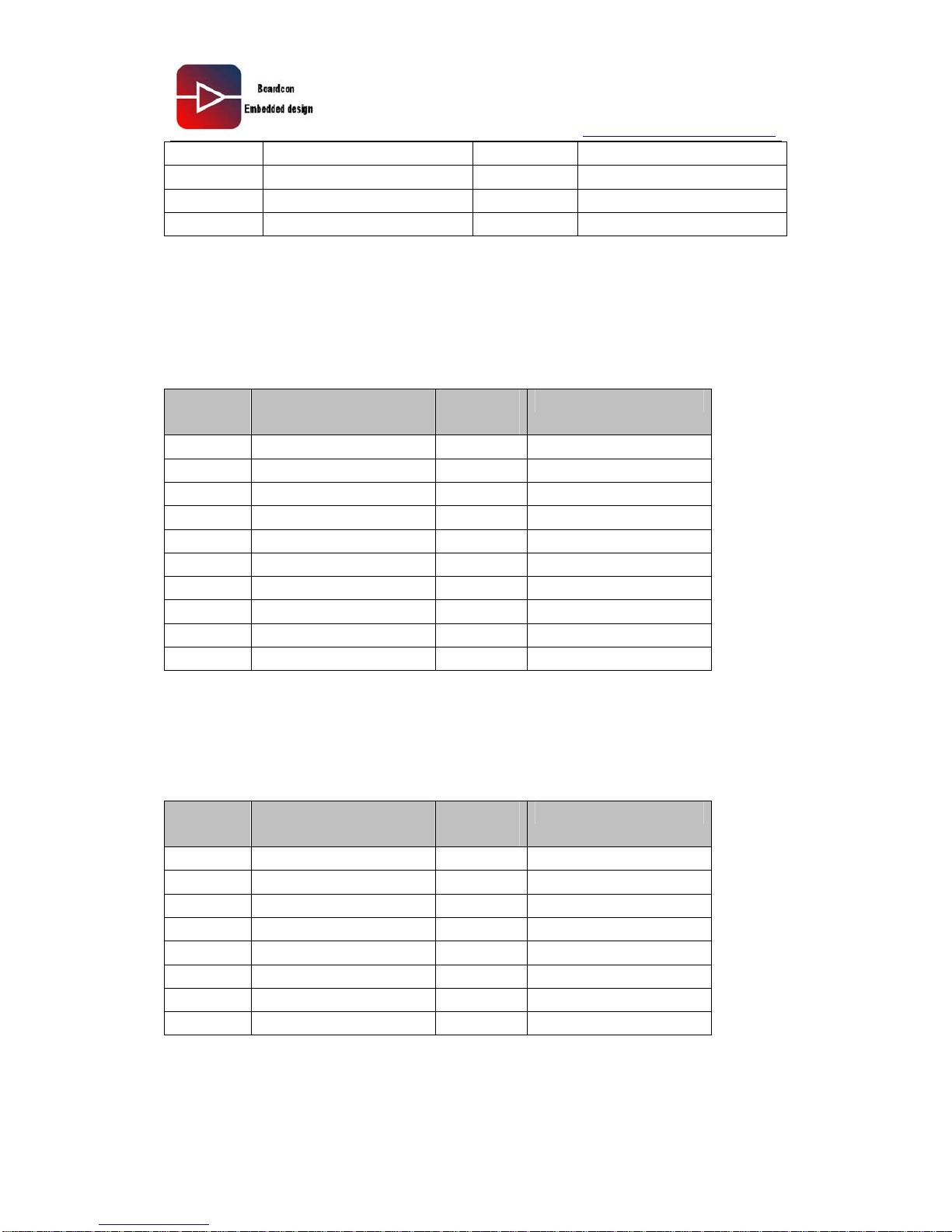
Page 46
www.armdesigner.com
Android6410 Reference Guide
46
17
LVD13
37
TSYM
18
LVD14
38
TSYP
19
LVD15
39
GND
20
LVD16
40
GND
4.4 J10.(CAMERA)
J10(CAMERA)pin definition:
Pin
number
Pin signal Pin
number
Pin signal
1
VDD_5V
11
LCAMDATA0
2
VDD_IO
12
LCAMDATA1
3
GND(R44)
13
LCAMDATA2
4
CAMRSTn
14
LCAMDATA3
5
LCAMPCLK
15
LCAMDATA4
6
CAM_SCL
16
LCAMDATA5
7
CAM_SDA
17
LCAMDATA6
8
LCAMVSYNC
18
LCAMDATA7
9
LCAMHREF
19
GND
10
LCAMCLK
20
GND
4.5 J12.(SDIO Module CH1)
J12(SDIO Module CH1)pin definition:
Pin nmber Pin signal Pin
number
Pin signal
1
SDCH1_WPn
9
SDCH1_CDn
2
SD1_VDD
10
GND
3
SDCH1_DATA1
11
SDCH1_CMD
4
SD1_VDD
12
GND
5
SDCH1_DATA0
13
SDCH1_DATA3
6
SD1_WIFI_RSTn
14
GND
7
SDCH1_CLK
15
SDCH1_DATA2
8
SD1_WIFI_PDn
16
GND
Page 47
www.armdesigner.com
Android6410 Reference Guide
47
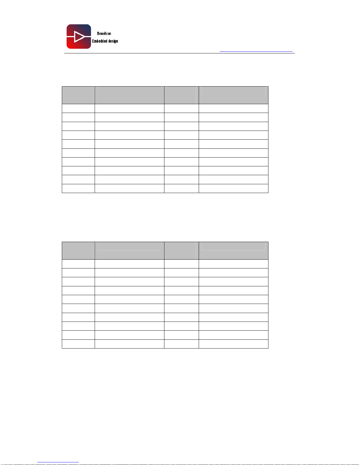
4.6. J22(SPI/AD)
J22(SPI/AD)pin definition:
Pin
nimber
Pin signal Pin
number
Pin signal
1
VDD_5V
11
EINT6
2
VDD_IO
12
EINT9
3
SPICS0
13
CLKOUT
4
SPIMISO0
14
NC
5
SPICLK0
15
ADCIN0
6
SPIMOSI0
16
ADCIN1
7
SPICS1
17
GND
8
SPIMISO1
18
GND
9
SPICLK1
19
GND
10
SPIMOSI1
20
GND
4.7. J20(KEYPAD)
J20(KEYPAD)pin definition:
Pin
nimber
Pin signal Pin
number
Pin signal
1
VDD_5V
11
KP_COL0
2
VDD_IO
12
KP_COL1
3
KP_ROW0
13
KP_COL2
4
KP_ROW1
14
KP_COL3
5
KP_ROW2
15
KP_COL4
6
KP_ROW3
16
KP_COL5
7
KP_ROW4
17
NC
8
KP_ROW5
18
NC
9
NC
19
GND
10
NC
20
GND
Page 48
www.armdesigner.com
Android6410 Reference Guide
48
5. WINCE6.0 Drive and Interface test
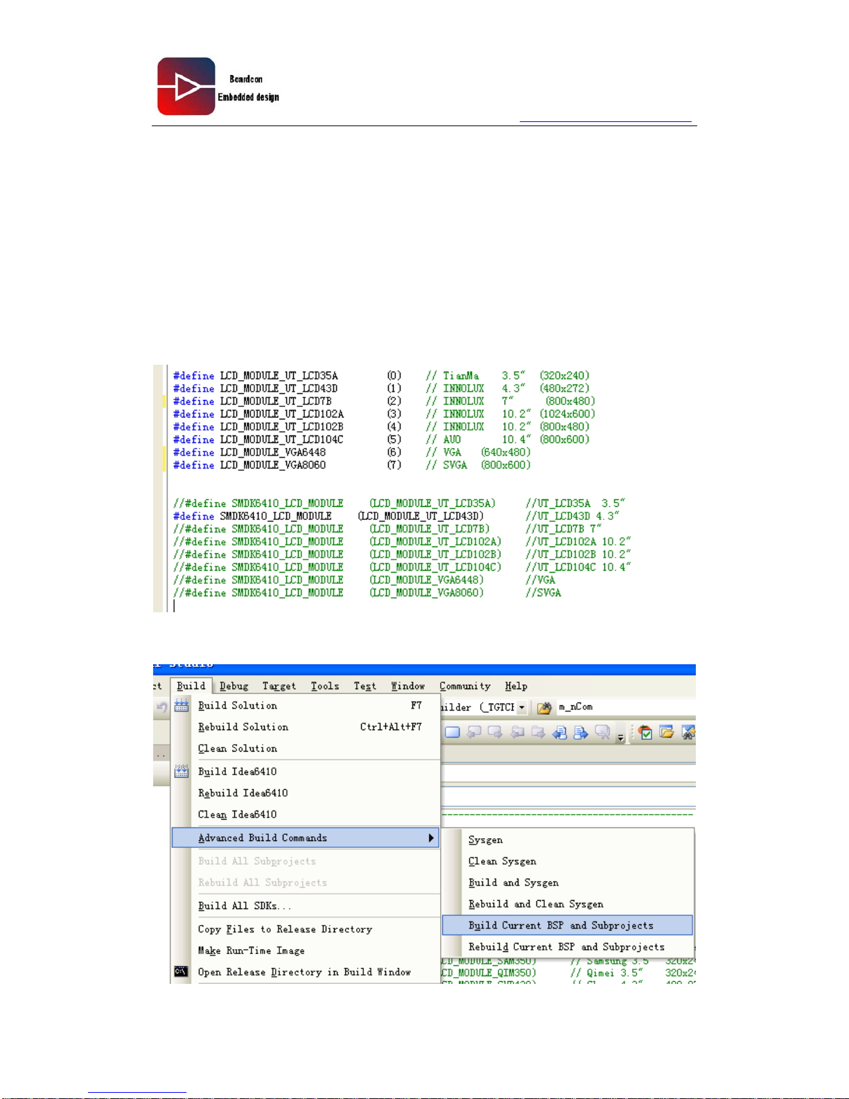
5.1. LCD Display Test
Android6410 BSP supports a variety of different types, different display resolution LCD
display in the factory, has been based on user selection (standard 4.3-inch) LCD screen is
the programming of the corresponding NK, we provide a simple drive changes in methods,
users can compile their own needs the corresponding NK.
Modify ◆ bsp_cfg.h in WINCE600\PLATFORM\SMDK6410\SRC\INC\。
◆ After changes, save the file, compile the BSP
Page 49

www.armdesigner.com
Android6410 Reference Guide
49
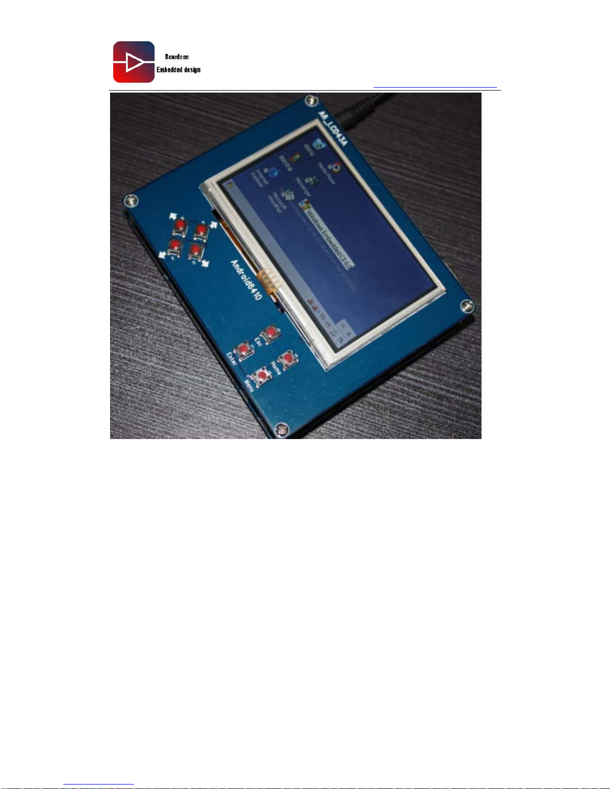
Take NK.bin boot into the board, connected to the corresponding liquid crystal screen, and
boot the system.
4.3 inch(480*272)
Page 50
www.armdesigner.com
Android6410 Reference Guide
50
5.2. TV OUT Test
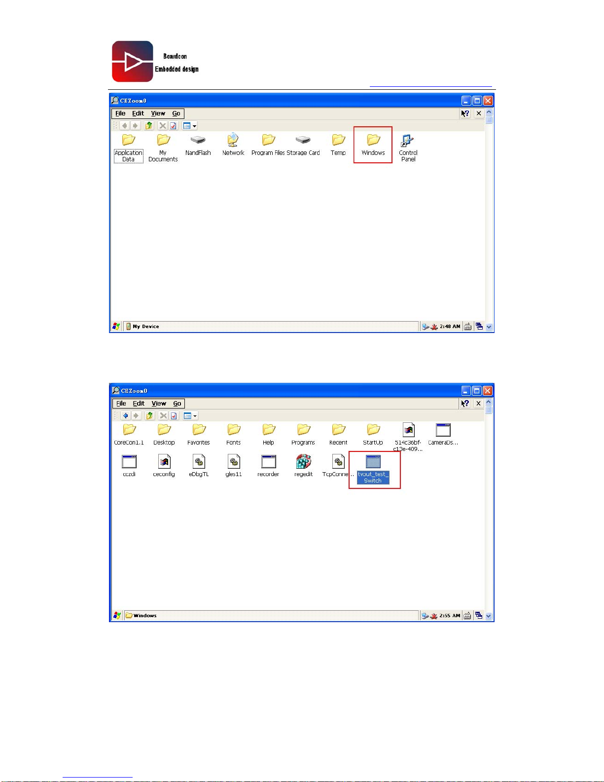
1.Take the television video signal line interface access to Single Board Computer Tv out
2. power on ,enter WinCE6.0,open “Mydevice”->“windows”
Page 51
www.armdesigner.com
Android6410 Reference Guide
51
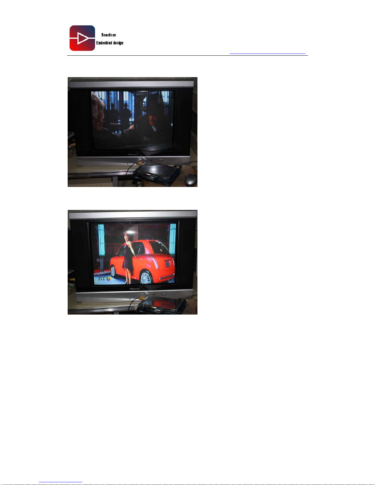
3、there is a tvout_test_Switch.exe under window, click it twiceand change output into
TV display.
Page 52
www.armdesigner.com
Android6410 Reference Guide
52
Play Video
5.3. Network port test
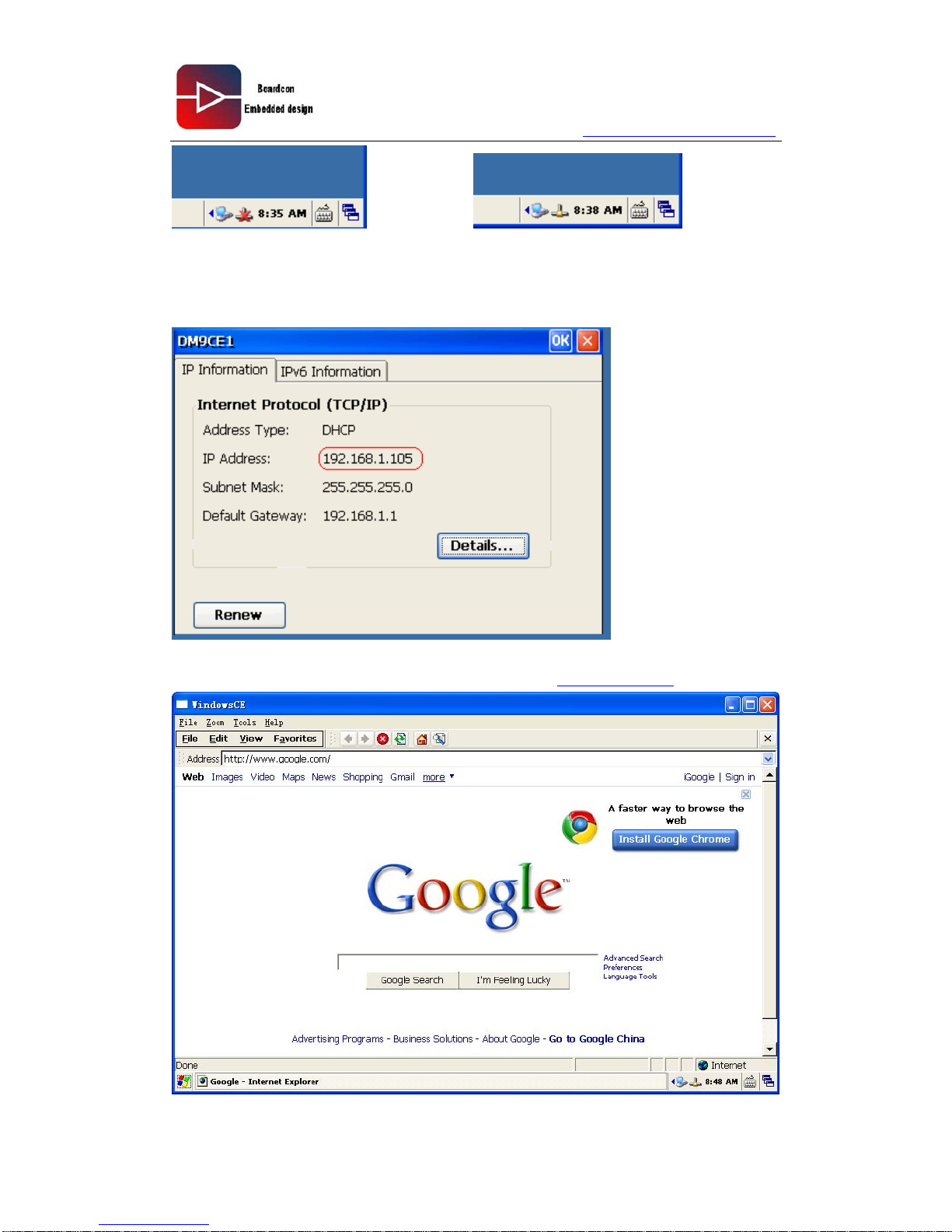
After boo◆ ting system, access Network Cable (one side of network line access to routing,
the other side access to RJ45 interface of Single Board Computer)
Cable access a few seconds, the net◆ work icon in the lower right foot into a connected
state from the disconnected
Page 53
www.armdesigner.com
Android6410 Reference Guide
53
Disconnected connected
Double◆ -click the network diagrams, and you can find that it is automatically assigned IP:
192.168.1.105
◆ double click the IE browser, login default home page www.google.com
Page 54
www.armdesigner.com
Android6410 Reference Guide
54
5.4. Audio Test
5.4.1. Audio Output Test
1. Take the headphones or speakers access to HEADPHONE Interface
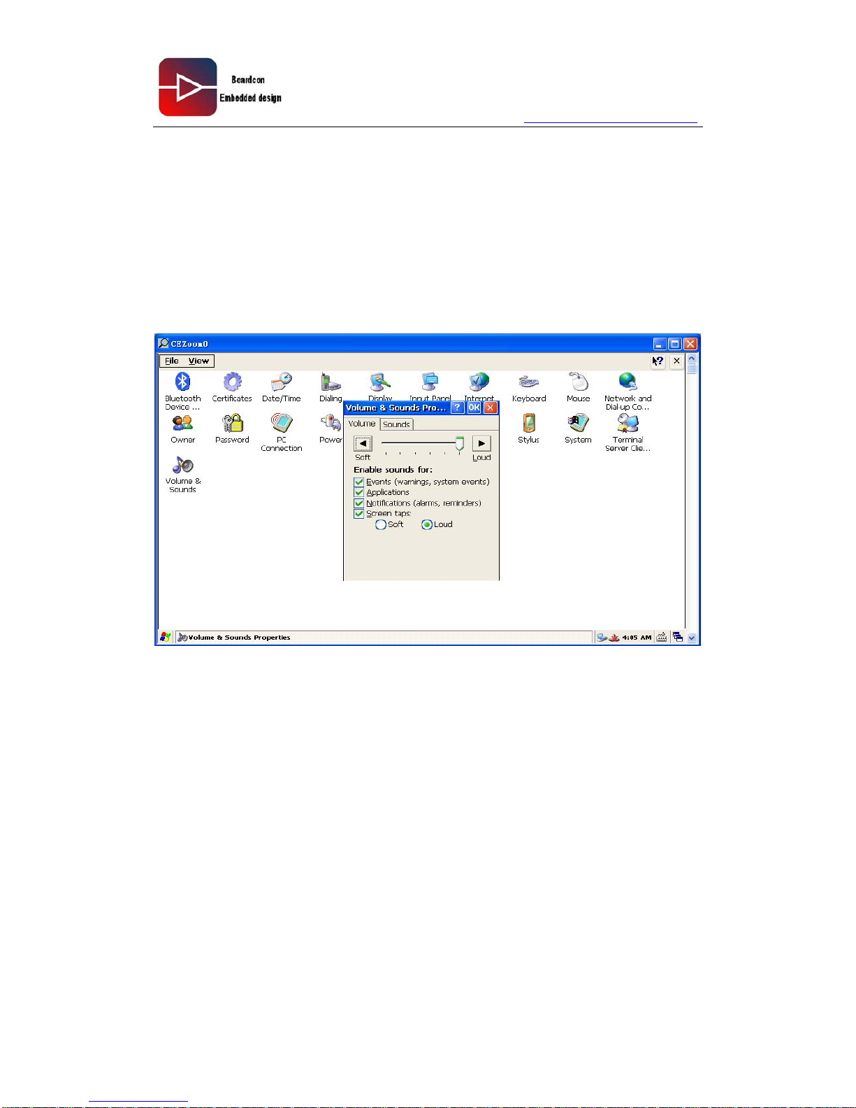
2. Open WinCE6.0 desktop "My Device" -> "Control Panel" -> "Volume & Sounds", by
change the test procedure to test sound setting
5.4.2. Audio input (recording) test
1. Inset the Mac to MIC interface
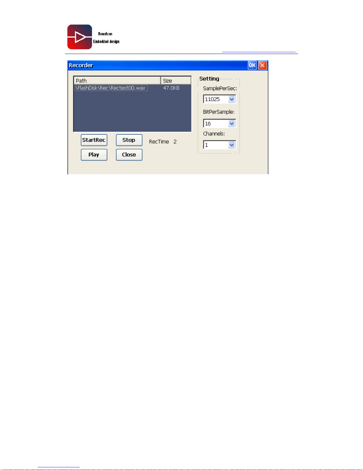
2. Plate: Test program \ wince test program \ Recorder copy the entire folder to wince
under the nandflash, double-click to open Recorder1.exe recording and playback test
3. Click the button to start recording StartRec
Page 55
www.armdesigner.com
Android6410 Reference Guide
55
4. Click the Stop button to stop recording, and click the "Play" to playback
5. Recording the audio files and save in the FlashDisk \ Rec \ under
5.5. USB Test
5.5.1. USB HOST Interface Test
5.5.1.1. USB Mouse Test
Insert the USB mouse to USB HOST interface, users are free to operate through the USB
mouse and test
5.5.1.2. USB Keyboard Test
Insert the USB keyboard to USB HOST interface, users can open WordPad to test
desktop keyboard all key functions.
5.5.1.3. U disk test
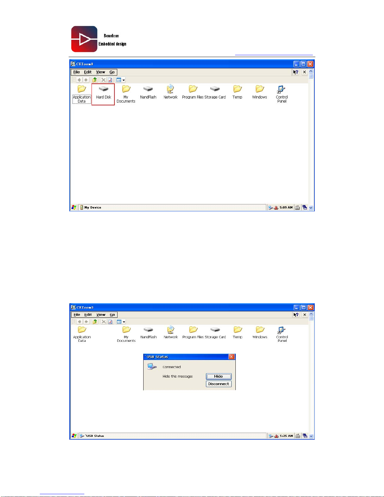
Inset U disk to the USB HOST interface, open the Desktop "My Device", you will see the
path the letter U disk
Page 56
www.armdesigner.com
Android6410 Reference Guide
56
5.5.2. USB OTG Interface Test
5.5.2.1. USB Device Synchronization Test
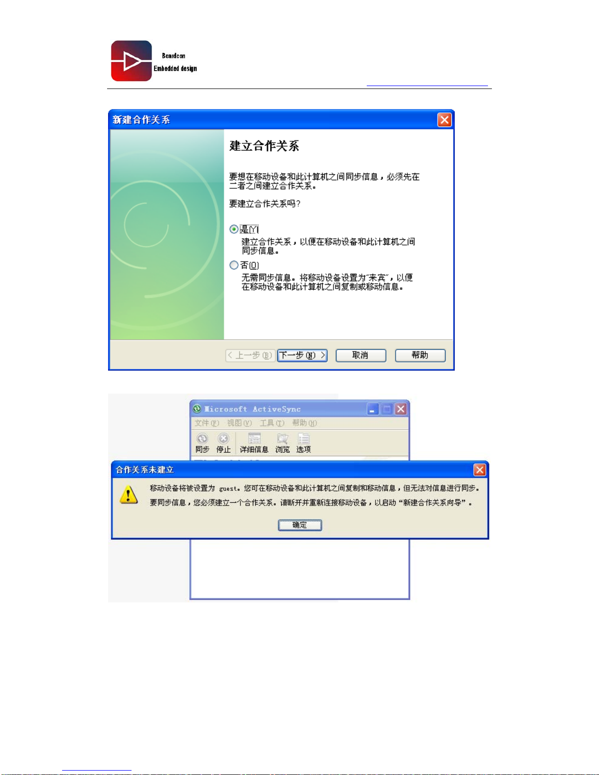
1. Inset the USB data cable to Single Board Computer and the PC, after booting into the
system, WinCE Sync will automatically link
Page 57
www.armdesigner.com
Android6410 Reference Guide
57
2, Click "Cancel"
3. Click "OK"
Page 58
www.armdesigner.com
Android6410 Reference Guide
58
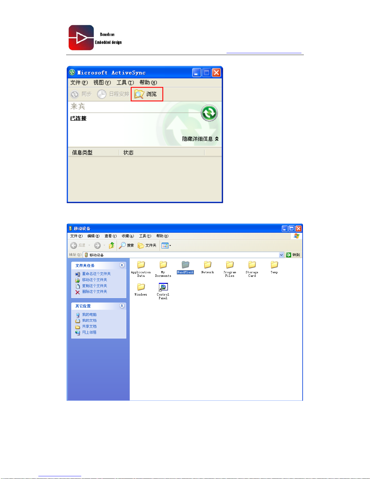
4. Click "Browse"
Synchronization has been established, can operate on PC Single Board Computer
interact with the data
Page 59
www.armdesigner.com
Android6410 Reference Guide
59
5.6. SD card Test
Android6410 Single Board Computer equipped with a high-speed SD card interface,
supports SD / MMC / SDHC / SDIO. Driver supports SD BUS2, theoretically maximum
support 32G.
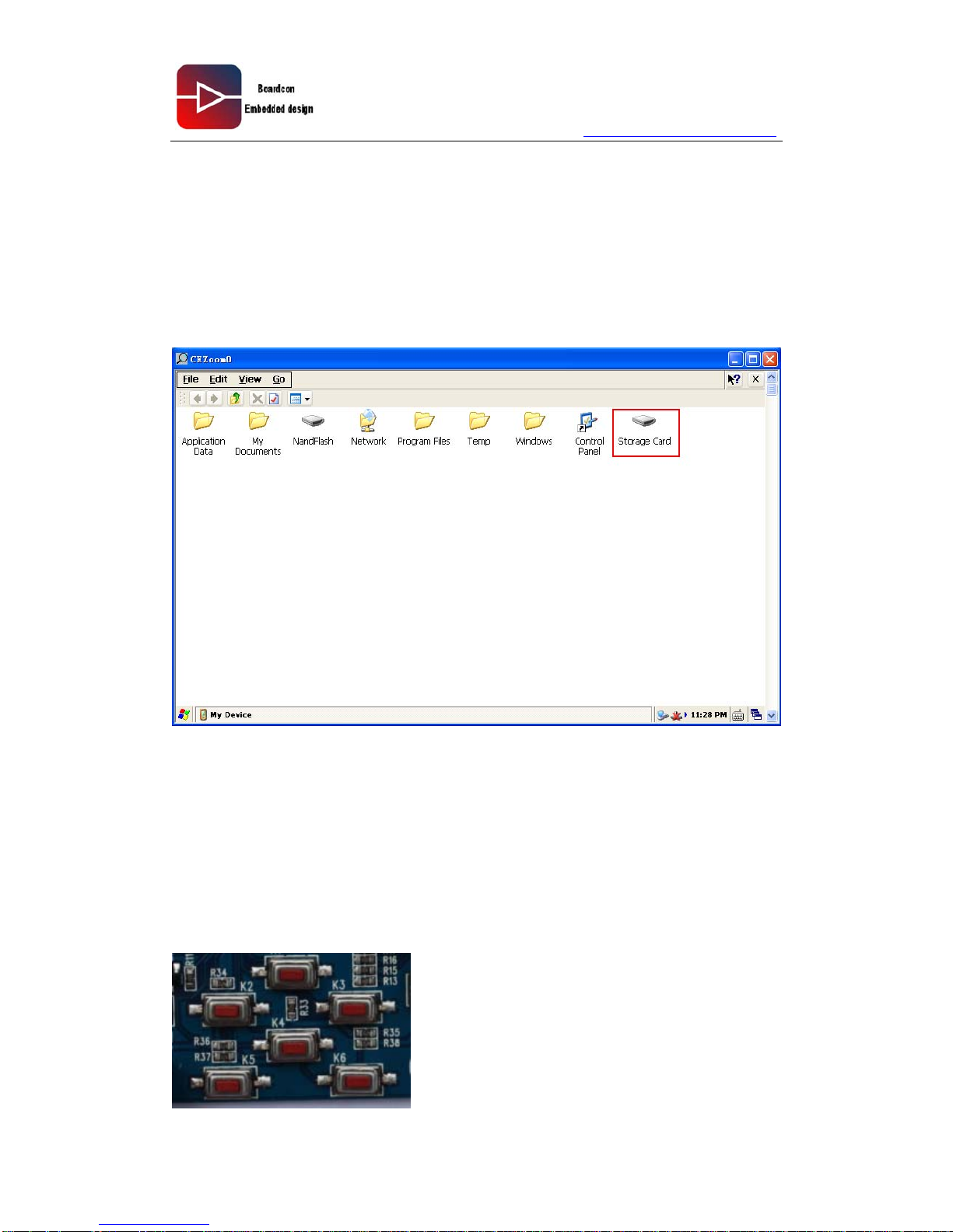
after the system starts, insert the SD card, under WinCE interface, you can see the SD
card drive letter: Storage Card
5.7. Button test
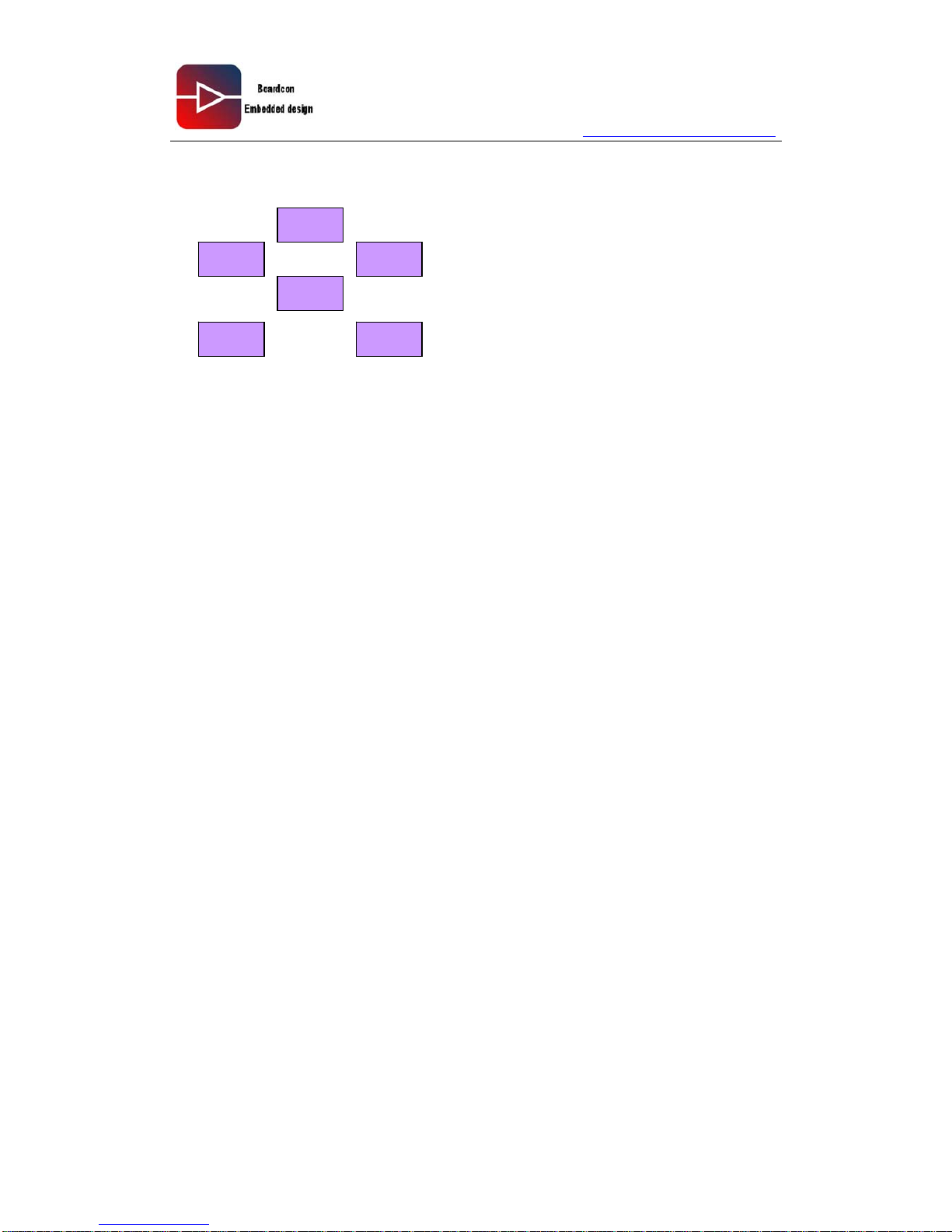
Android6410 designed 6 keys for users, key functions through GPIO interface to realize.
Key support interrupt mode and query mode, function realization, down, left, right, OK, to
return. Users can control and program it based on their own needs. User button interface
to physical Map:
Page 60
www.armdesigner.com
Android6410 Reference Guide
60
The default function key definitions
6. WINCE6.0 Multimedia Hardware
Codec Test
6.1. TCPMP player testing (hardware decoding)
TCPMP player is open source player, users can download the source code version from
network to migrate, Android6410 provides a TCPMP_Debug CD player, Shenzhen youjian
Hangtian science and technology research and development of products on their own, the
player built-in a hardware decoder based on S3C6410 to support
H264/MPEG-4/H263/VC-1 video formats D1 (720 * 576) resolution, a perfect audio and
video decoding, decoding rate in more than 30fps.
character
1、MPEG-4 simple profile
2、H.264/AVC baseline
3、H.263 P3
4、VC-1(WMV9) main profile
6、Support the extension, including avi, mp4, m4v, mov, 3gp, flv, mpg video files and
other common
7. Support DIVX、XVID
8、Video decoding at 30 frames / sec or above
9、Video playback smooth, clear
10. support audio decoding MP1、MP2、MP3、AC3、AAC etc.
Here on the Android6410 through TCPMP player Single Board Computer to test the
performance of multimedia decoding
Left Right
Up
Down
Back Enter
Page 61
www.armdesigner.com
Android6410 Reference Guide
61
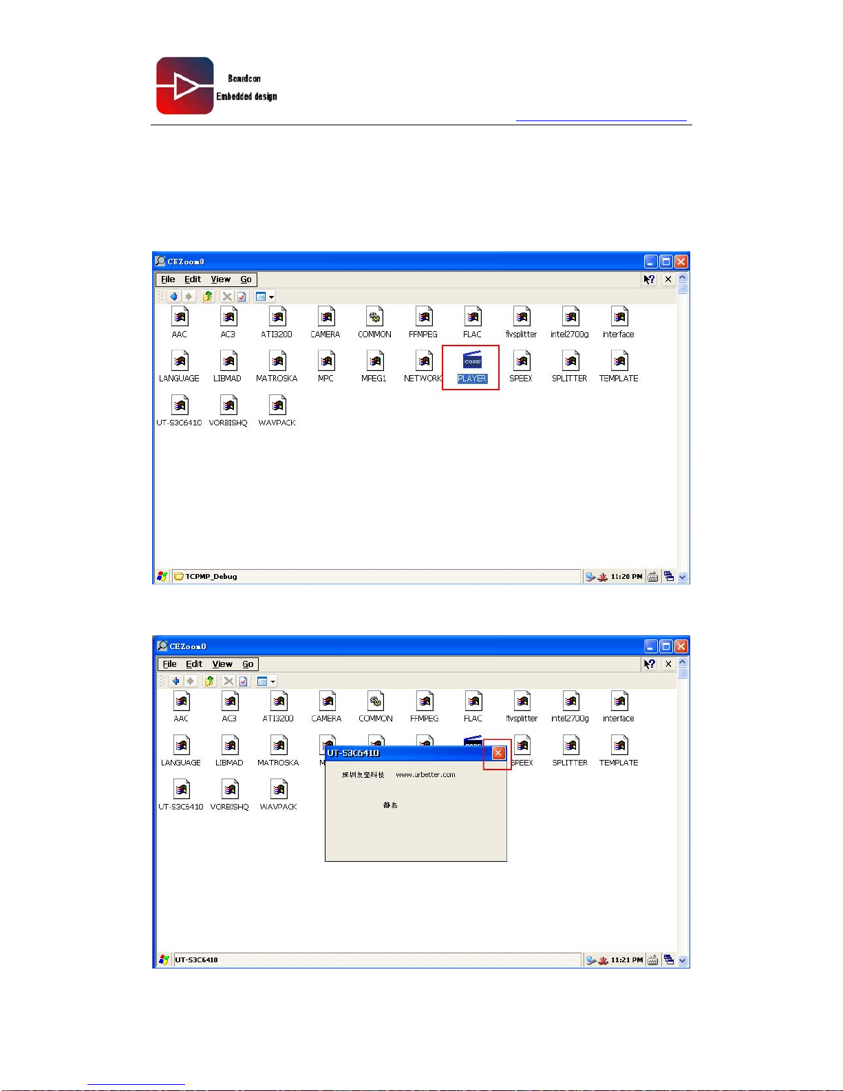
1, The CD-ROM: \ test program \ wince test program \ TCPMP_Debug and copied to the
SD card Video Demo
2, Start the Single Board Computer -> enter WinCE6.0 System -> insert the SD card ->
direct double-click to open
Storage Card\TCPMP_Debug\PLAYER.exe
3. Directly turn off the prompt box
Page 62
www.armdesigner.com
Android6410 Reference Guide
62
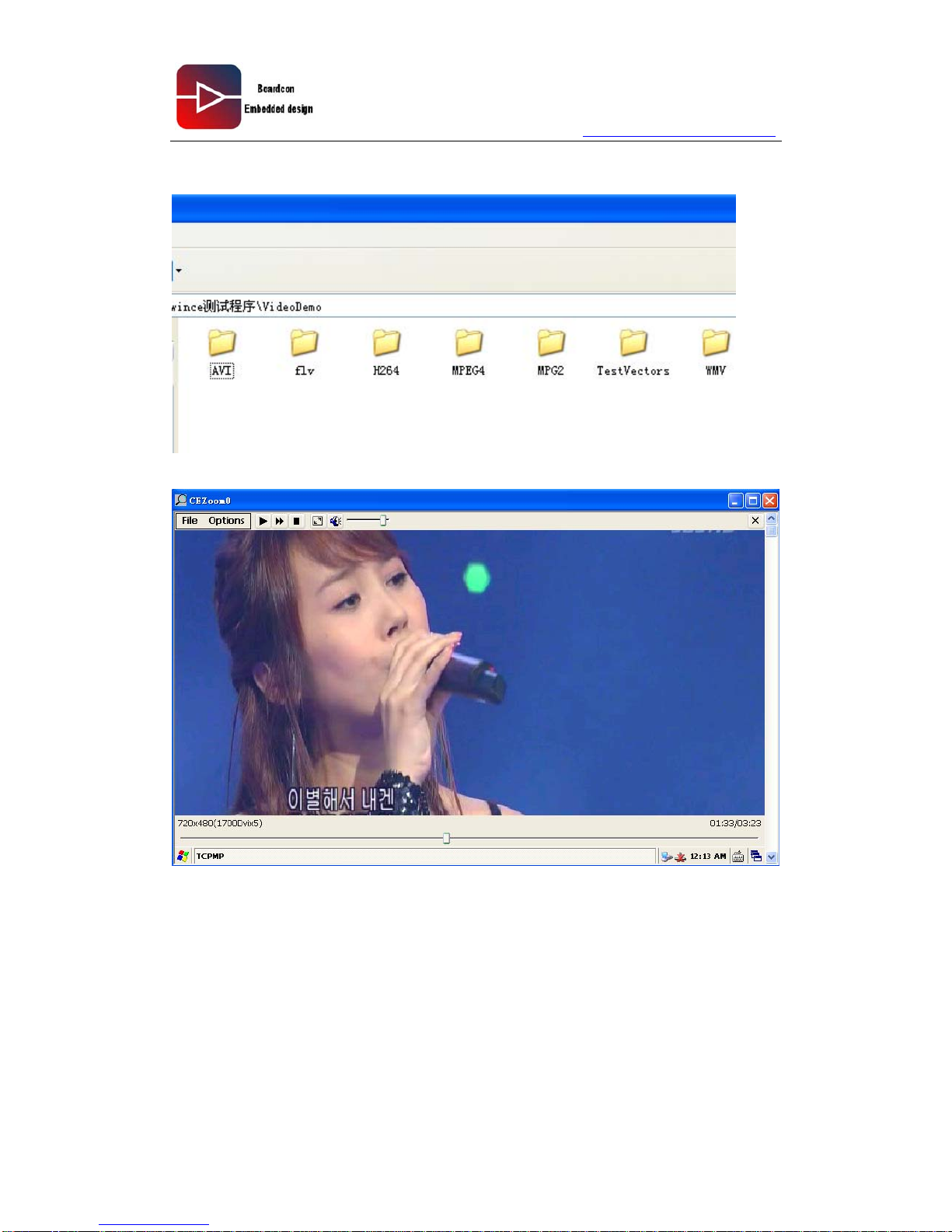
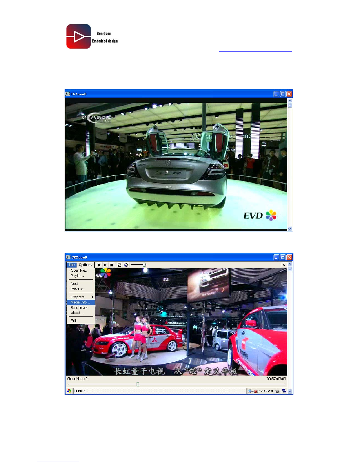
4. Video Demo provides multiple video test file, the user can test the performance
Page 63
www.armdesigner.com
Android6410 Reference Guide
63
5, Where we choose a H264 video, resolution 720 * 480, to test it under the Single Board
Computer 7-inch screen (resolution 800 * 480) .Open VideoDemo \ H264 \
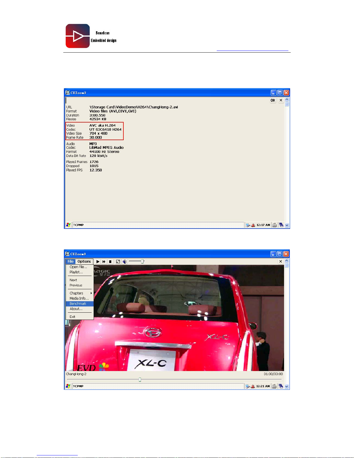
ChangHong-2.avi
6. View the video film source information: File-> Media Info .....
Page 64
www.armdesigner.com
Android6410 Reference Guide
64
Codec: UT-S3C6410 H264 shows that use H264 hardware decoder made by
youjian technology to hardware solute
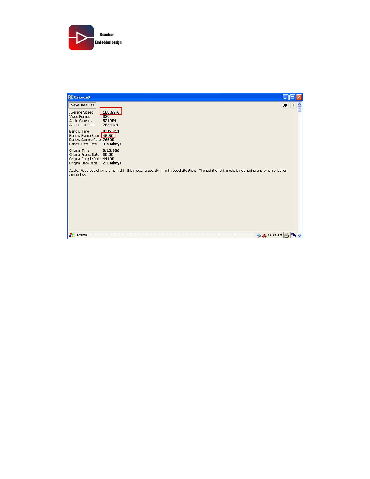
7. Test hardware acceleration: File -> Benchmark
Page 65
www.armdesigner.com
Android6410 Reference Guide
65
Test results:
Full screen D1 resolution H264 video file 160% efficiency, decoding speed of 48.3 / s
Page 66
www.armdesigner.com
Android6410 Reference Guide
66
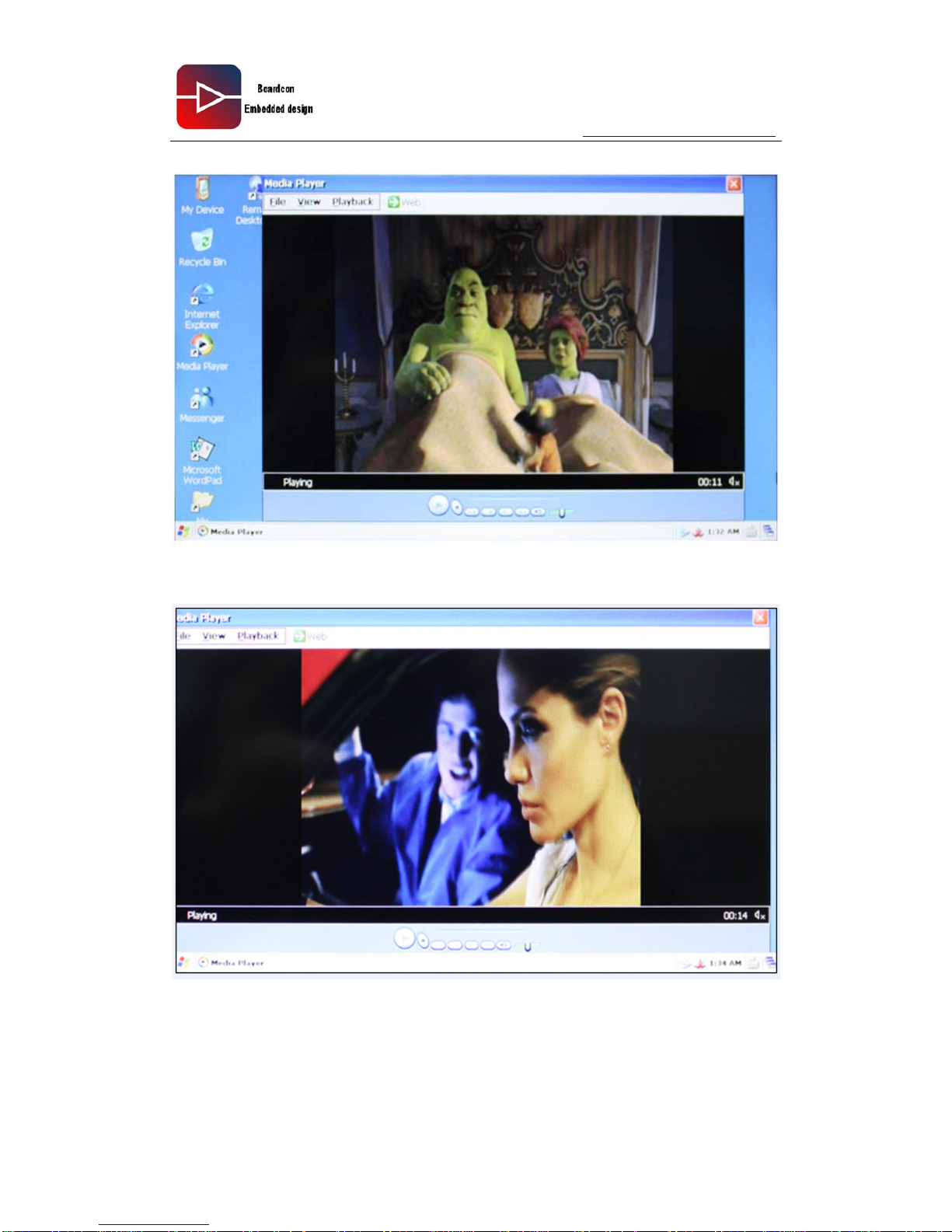
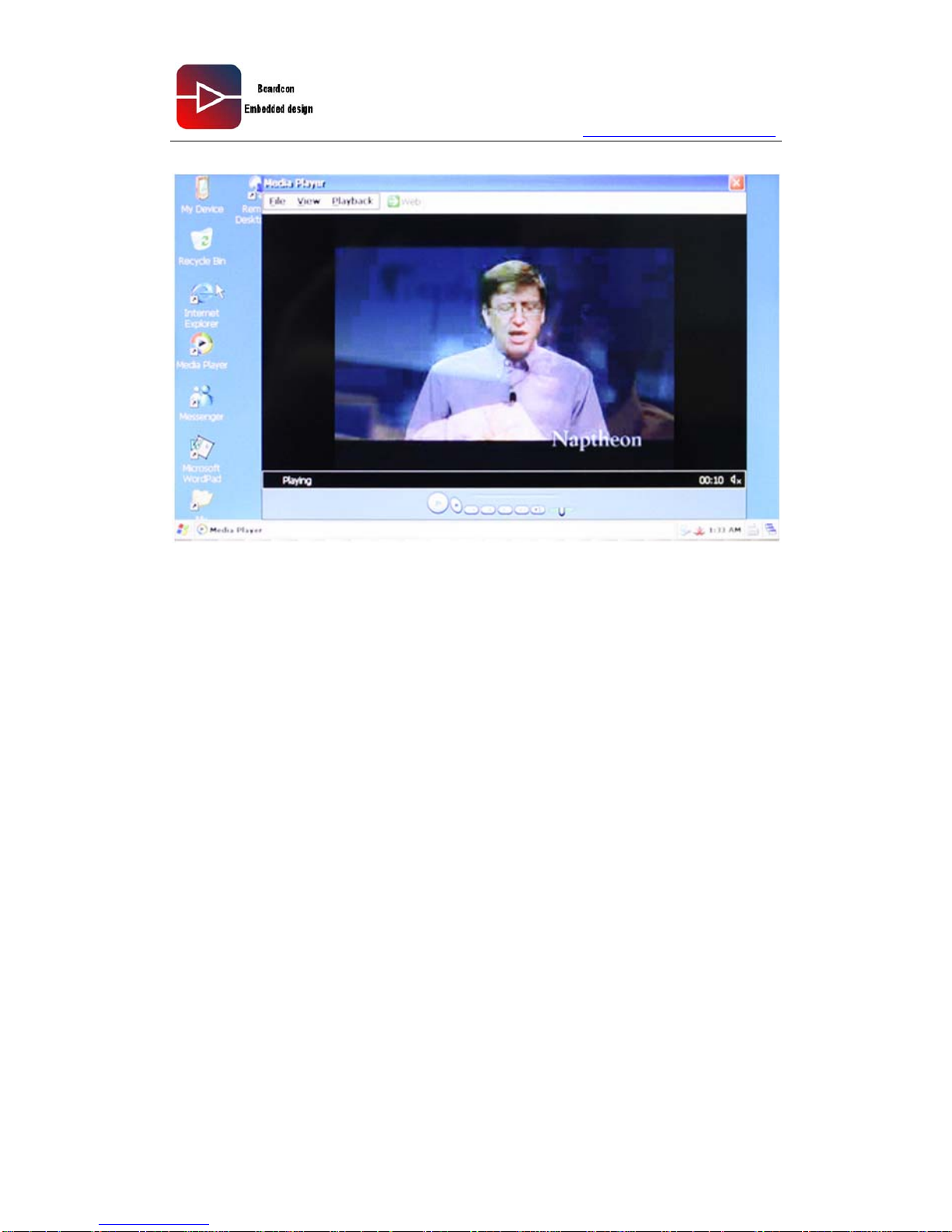
6.2. Media Player Test(DirectShow Filters)
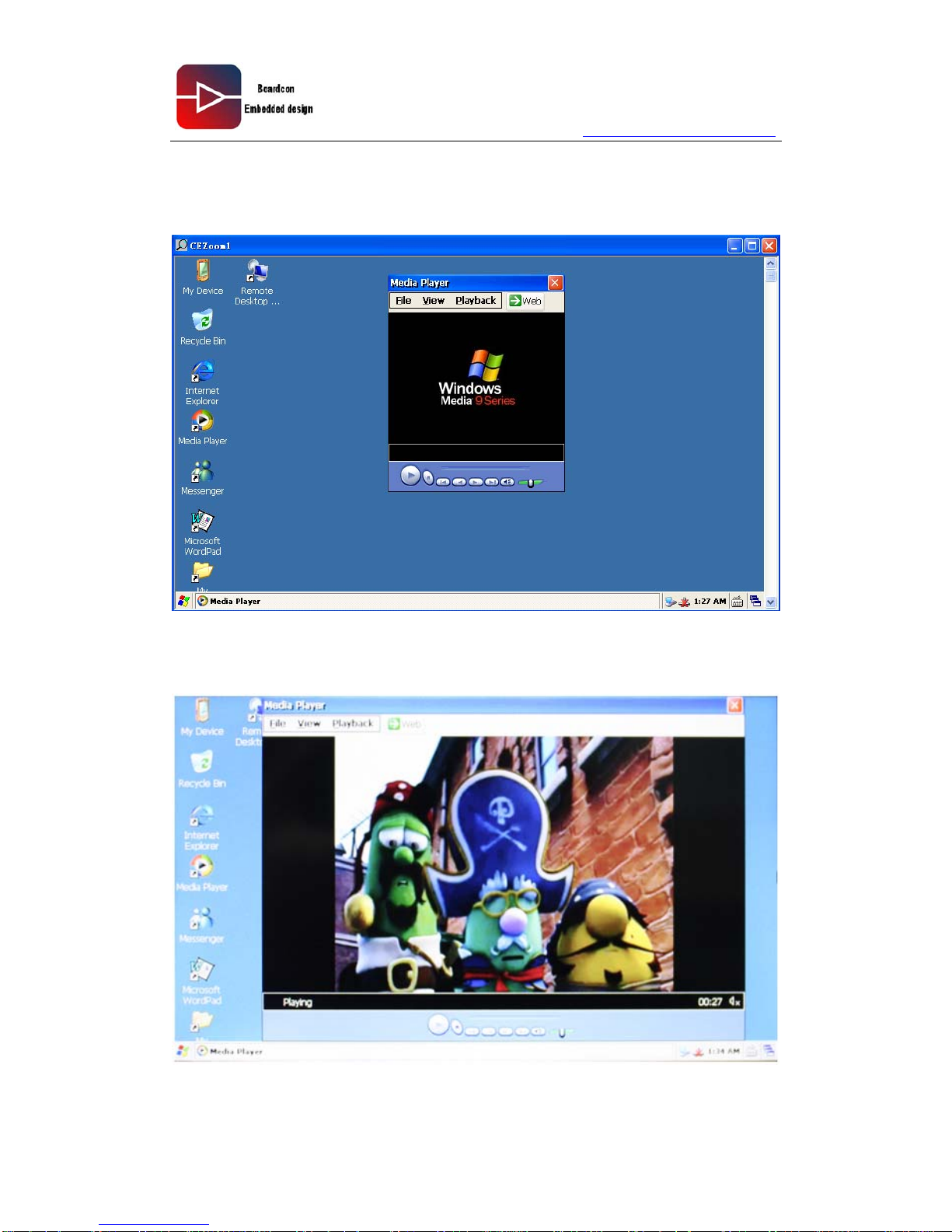
1. Open the Desktop Media Player
2. "File-> Open" to open \ VideoDemo \ TestVectorsem \ next to test the video file
Play H264
Page 67
www.armdesigner.com
Android6410 Reference Guide
67
Play MP4
Play H263
Page 68
www.armdesigner.com
Android6410 Reference Guide
68
Play VC-1
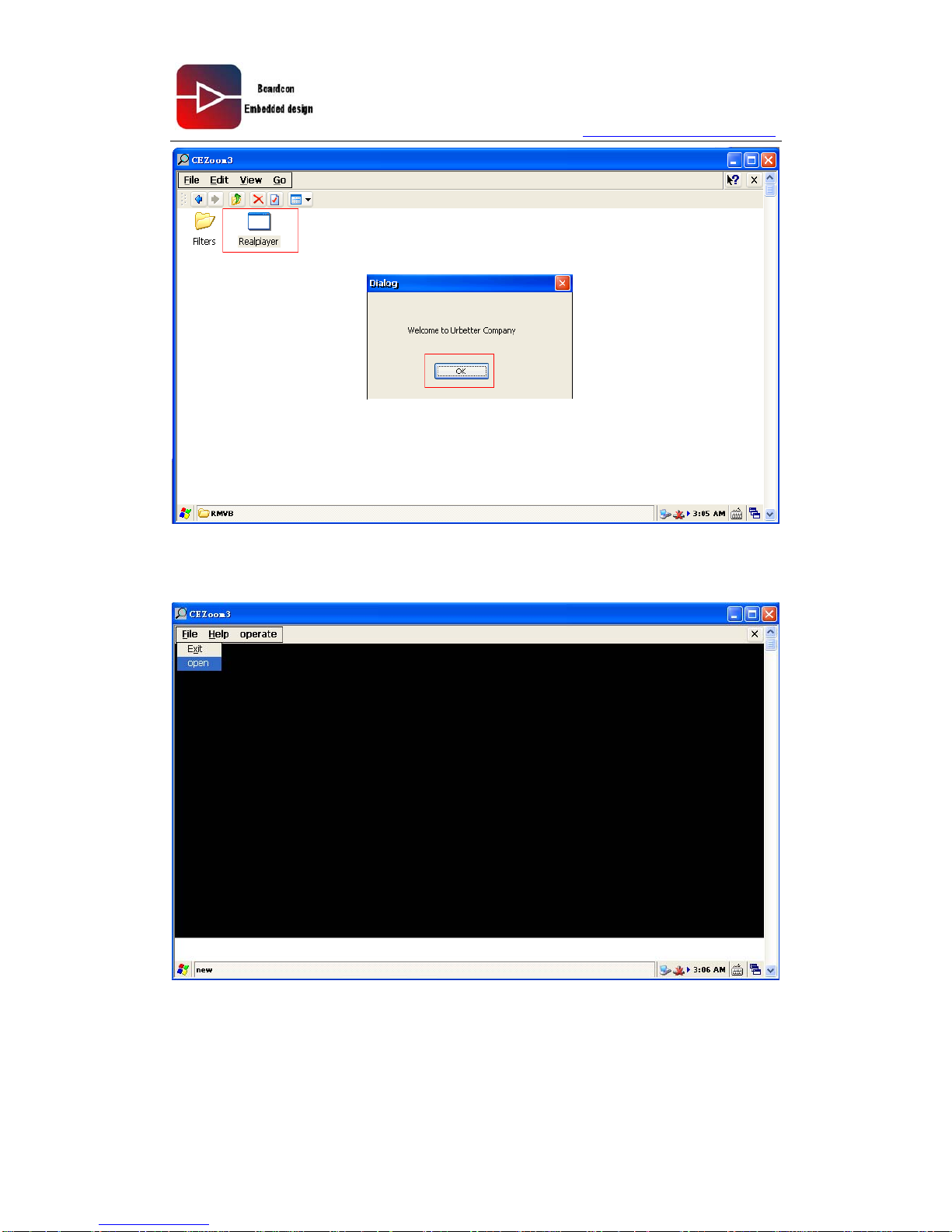
6.3. RMVB Player Test
RMVB player is another a multimedia player of Youjian hentian technology company, this
player can decode rm, rmvb video well,
1. Copy the entire folder in \ test program \ wince test program \ RMVB to wince
2, Double-click to open RMVB \ Realplayer.exe, pop-up dialog box, click "OK"
Page 69
www.armdesigner.com
Android6410 Reference Guide
69
3, Click on File-> open, open VideoDemo \ RMVB \ test files to test
Play "Prison Break" download from the website
Page 70

www.armdesigner.com
Android6410 Reference Guide
70
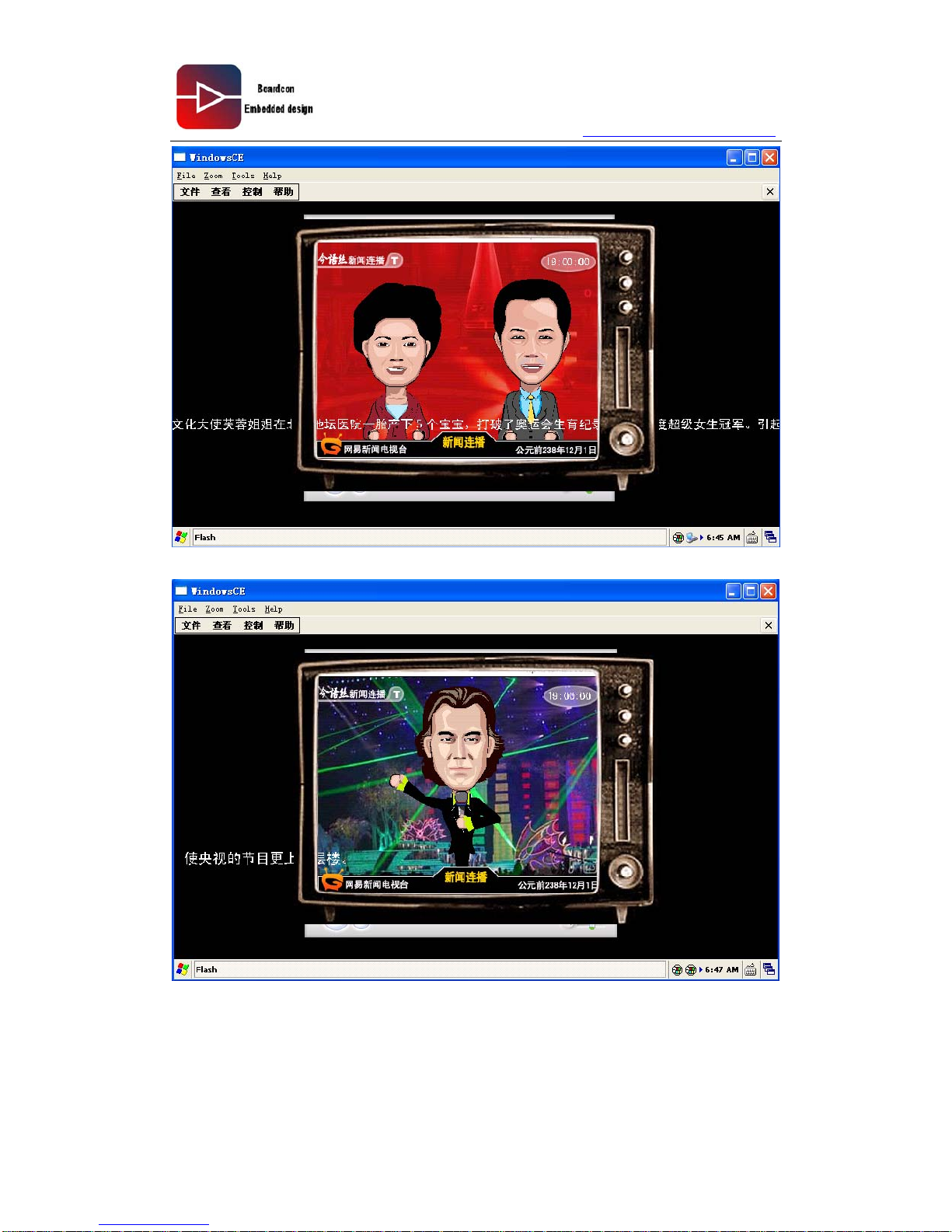
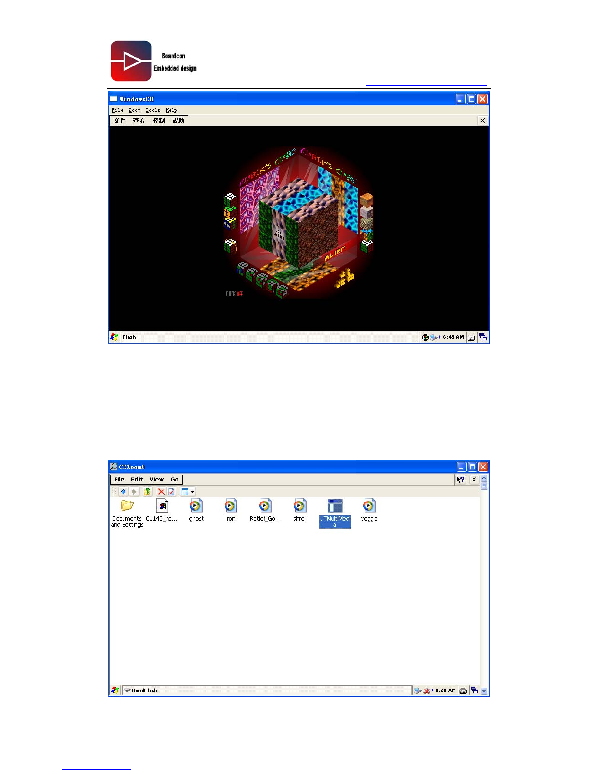
6.4. FLASH Player Test
1, The CD-ROM path:copy the entire folder in \ test program \ wince test program \ Flash
to wince, directly open the directory Flash.exe
2, Through the "File" -> "Open", find the Flash test file folder, and open
Page 71
www.armdesigner.com
Android6410 Reference Guide
71
Page 72
www.armdesigner.com
Android6410 Reference Guide
72
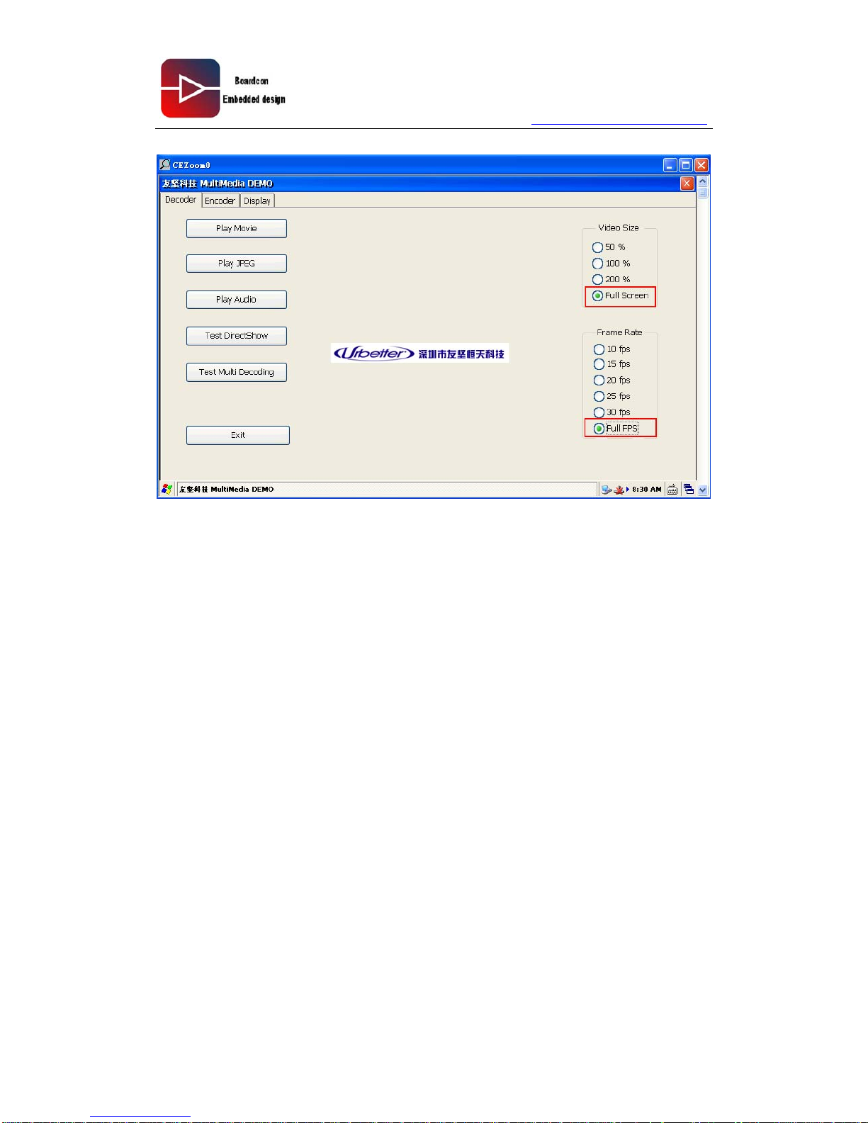
6.5. MultiMedia Test
1. The CD-ROM path: copy all files in \ test program \ wince test program \
MultiMediaDemo \to NandFlash in WINCE6.0
Page 73
www.armdesigner.com
Android6410 Reference Guide
73
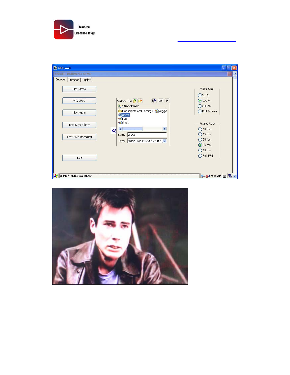
2、Double click and open UTMultiMedia.exe
Page 74
www.armdesigner.com
Android6410 Reference Guide
74
6.5.1. Play Movie
Page 75
www.armdesigner.com
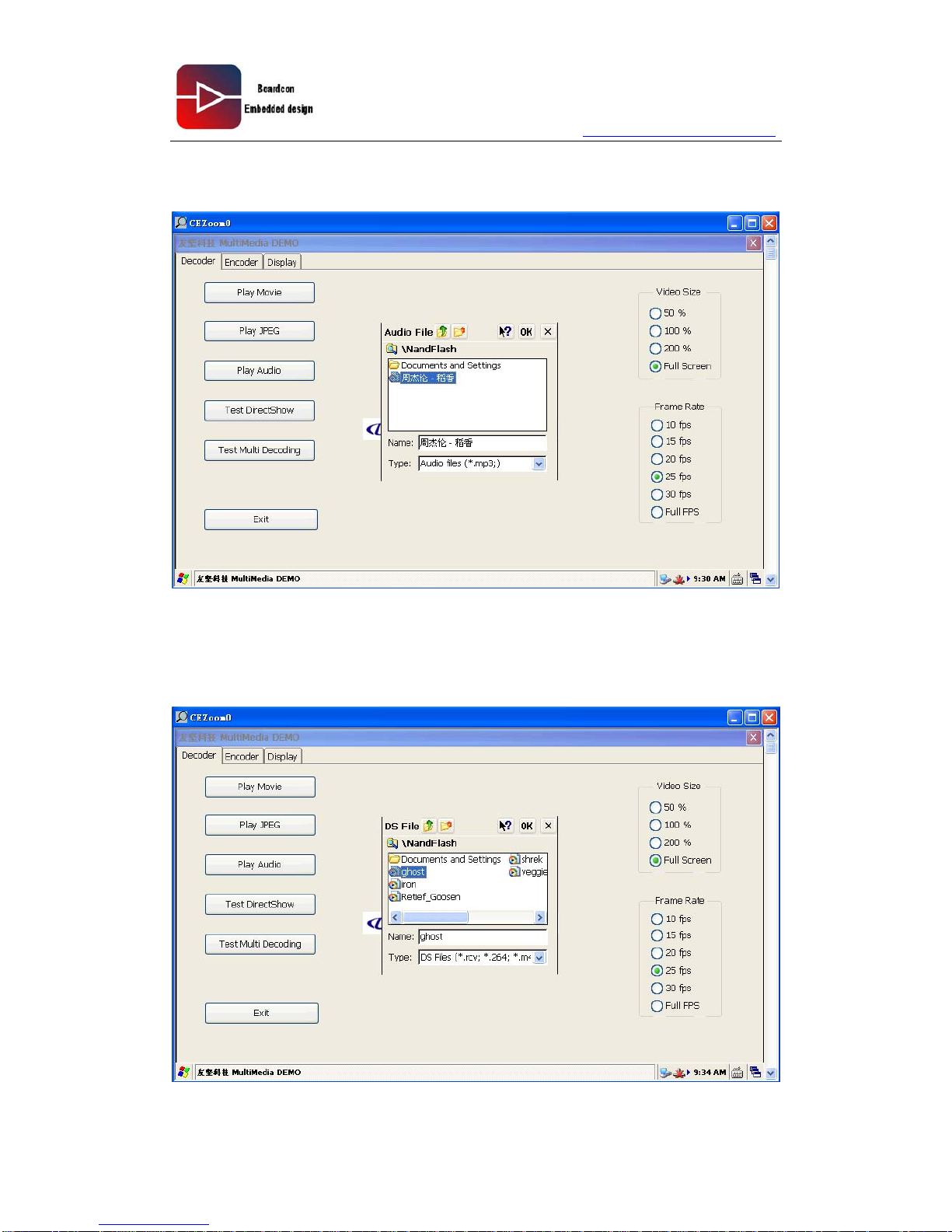
Android6410 Reference Guide
75
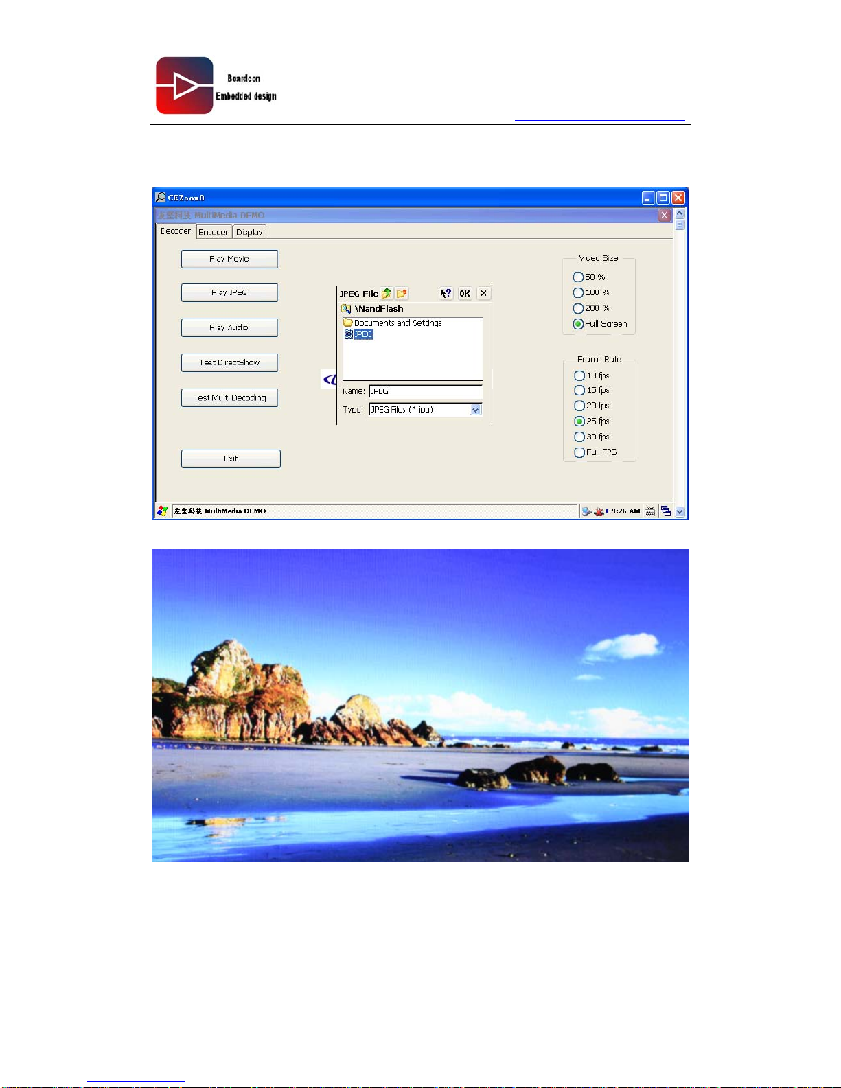
6.5.2. Play JPEG
Page 76
www.armdesigner.com
Android6410 Reference Guide
76
6.5.3. Play Audio
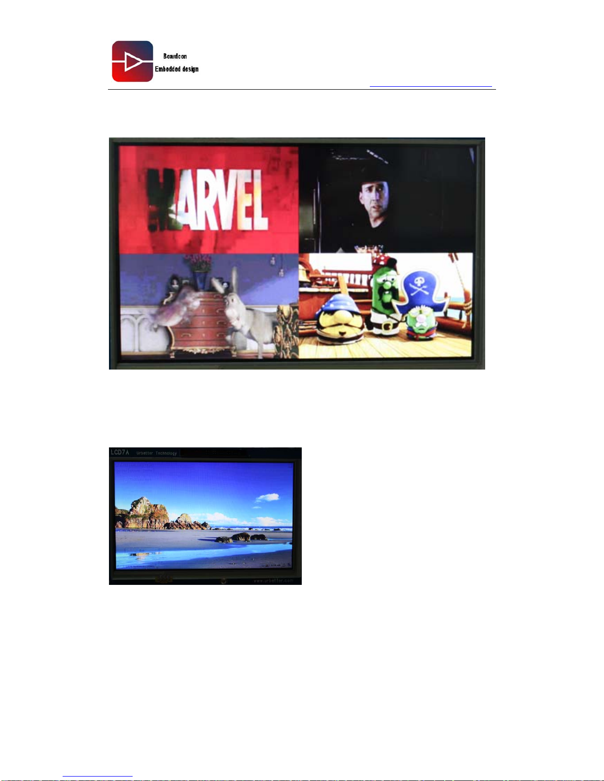
6.5.4. Test DirectShow
Page 77
www.armdesigner.com
Android6410 Reference Guide
77
6.5.5. Test Multi Decoding
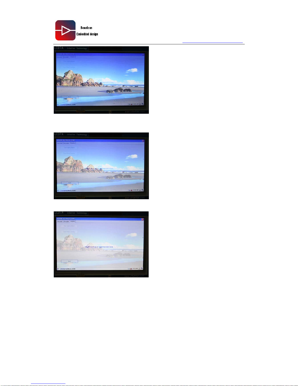
6.5.6. Test Alpha Blend
Page 78
www.armdesigner.com
Android6410 Reference Guide
78
Page 79
www.armdesigner.com
Android6410 Reference Guide
79
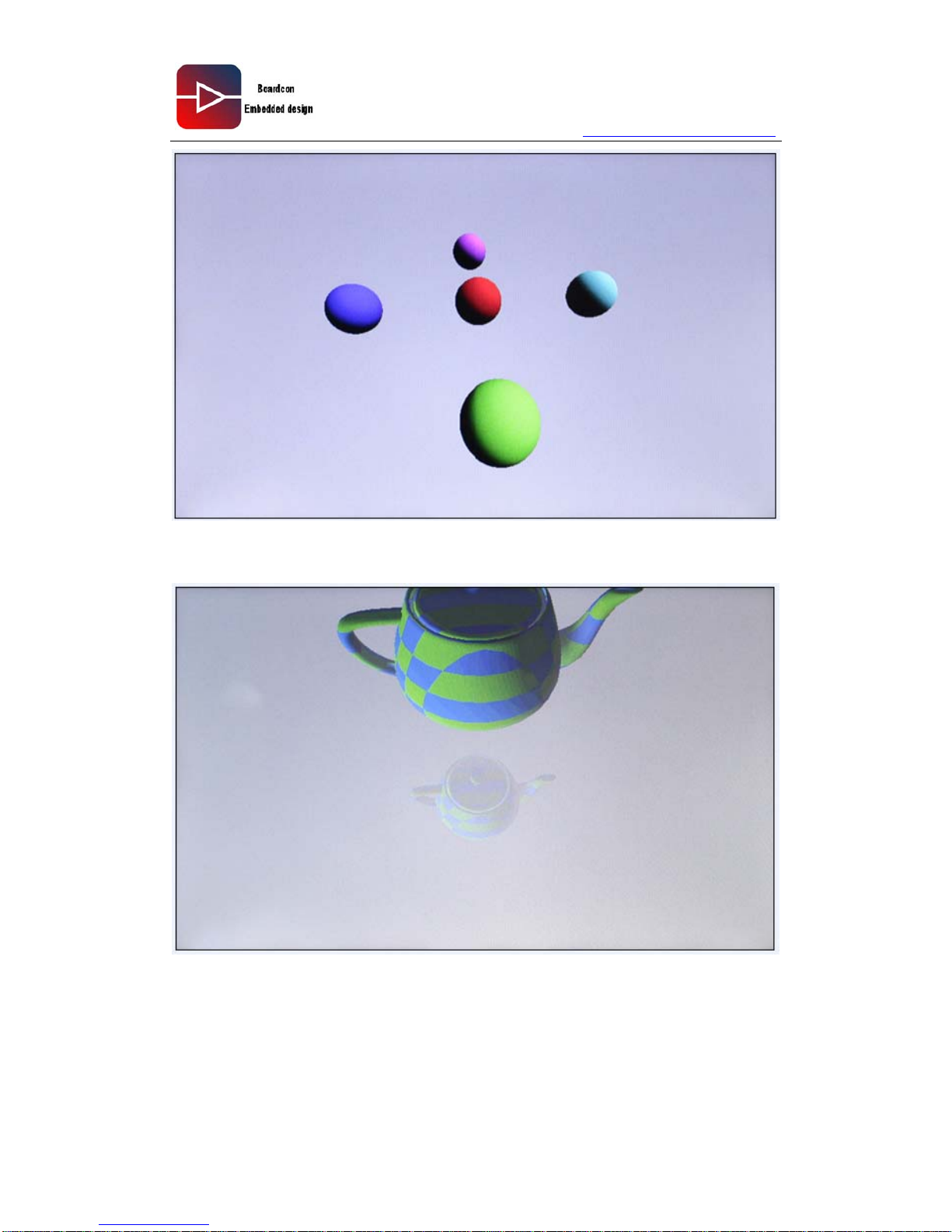
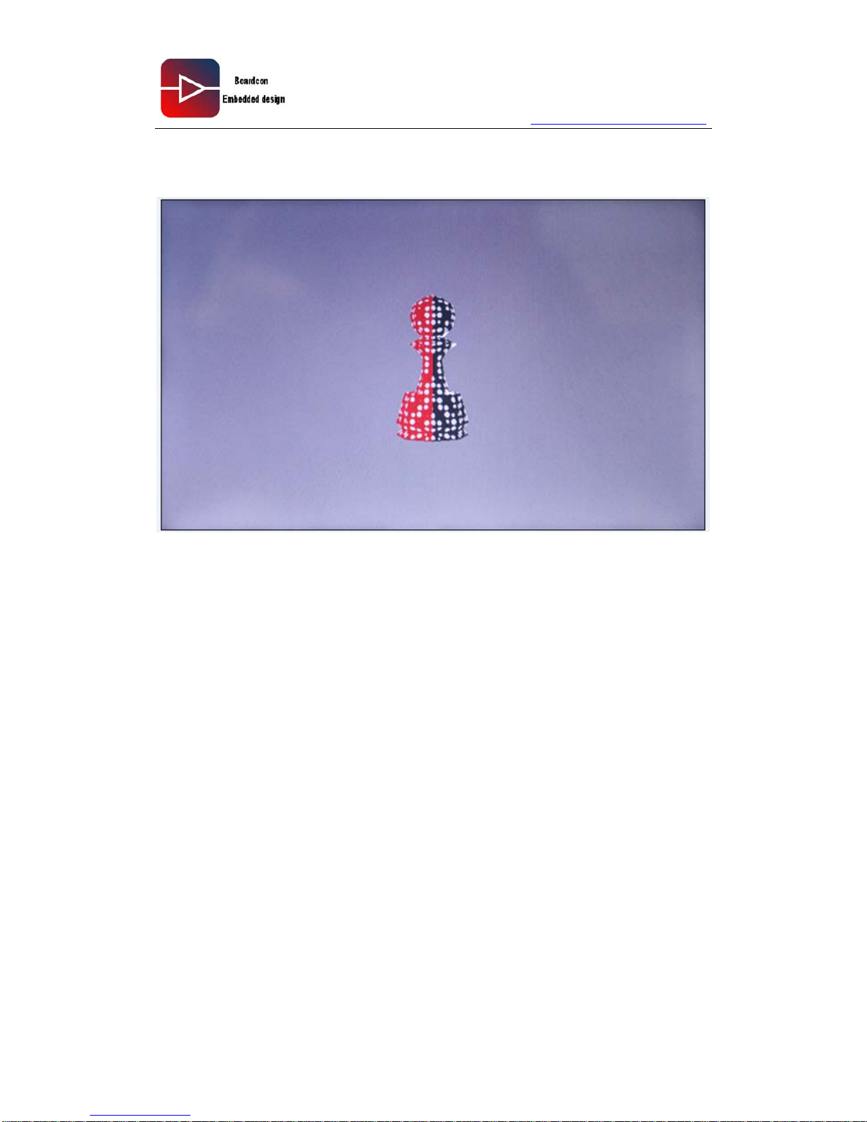
6.6. 3DGraphics Hardware Acceleration Test
(OPENGLES1.1&2.0)
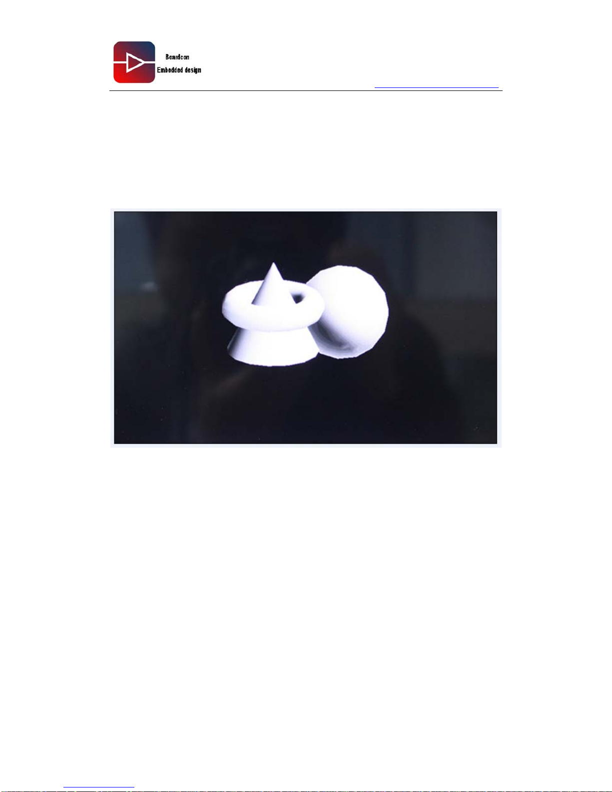
6.6.1. OpenGles 1.1 Test
Page 80
www.armdesigner.com
Android6410 Reference Guide
80
Page 81
www.armdesigner.com
Android6410 Reference Guide
81
6.6.2. OpenGles 2.0 Test
6.7. JPEG Hardware Decoding Test
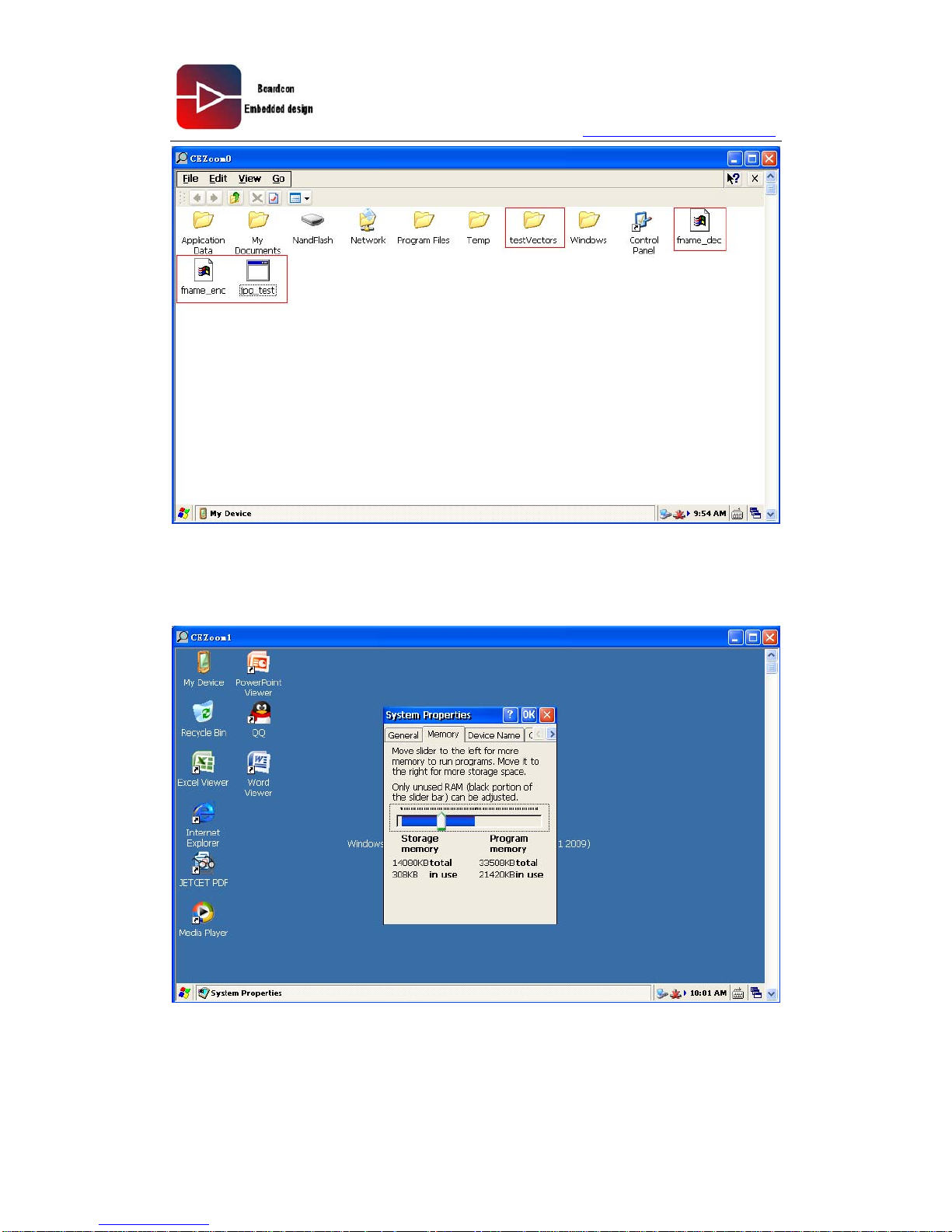
1. The CD-ROM path: copy all files in \ test program \ wince test program \ JPEG_test \
to WINCE6.0 root catalog
Page 82
www.armdesigner.com
Android6410 Reference Guide
82
Note: If you are prompted to copy the process memory space, you can right click on the
desktop "My Device" to set the storage space, because we only copy the file in. 14M, all
just need to set the storage space can be larger than 14M
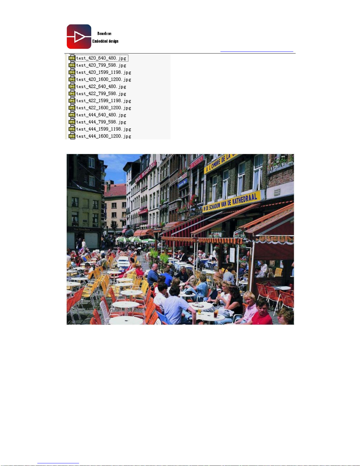
2、Double click jpg_test.exe to do JPEG hardware decoding test
The procedures will do hardware decoding to the following respective rates of JPEG
pictures
Page 83
www.armdesigner.com
Android6410 Reference Guide
83
Page 84
www.armdesigner.com
Android6410 Reference Guide
84
7. LINUX device driver and interface
testing
7.1. LCD Test
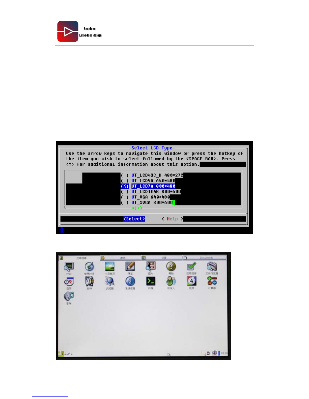
When Users are configuring the kernel: making menuconfig, they can choose LCD type
according to their choice of LCD module, compile the final programmed zImage to Single
Board Computer, the system starts to the download LCD driver at system startup is the
type of the corresponding LCD.
The following is UT_LCD7A display module:
Page 85
www.armdesigner.com
Android6410 Reference Guide
85
7.2. Touch Screen Test and Calibration
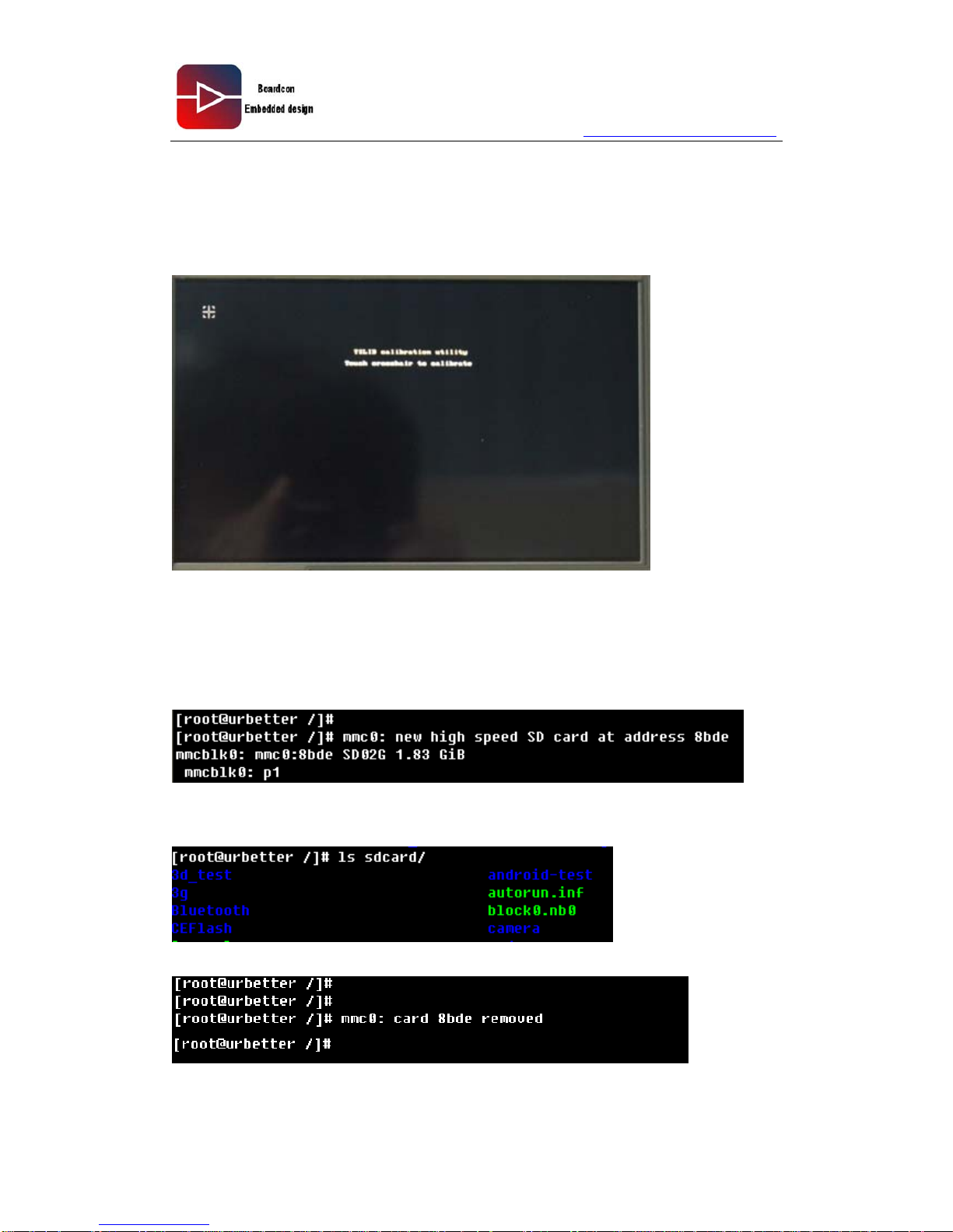
After the system starting, under the QT interface of "Setting" column, there is a
"re-calibration", open the re-calibration procedures to correct
7.3. SD card Test
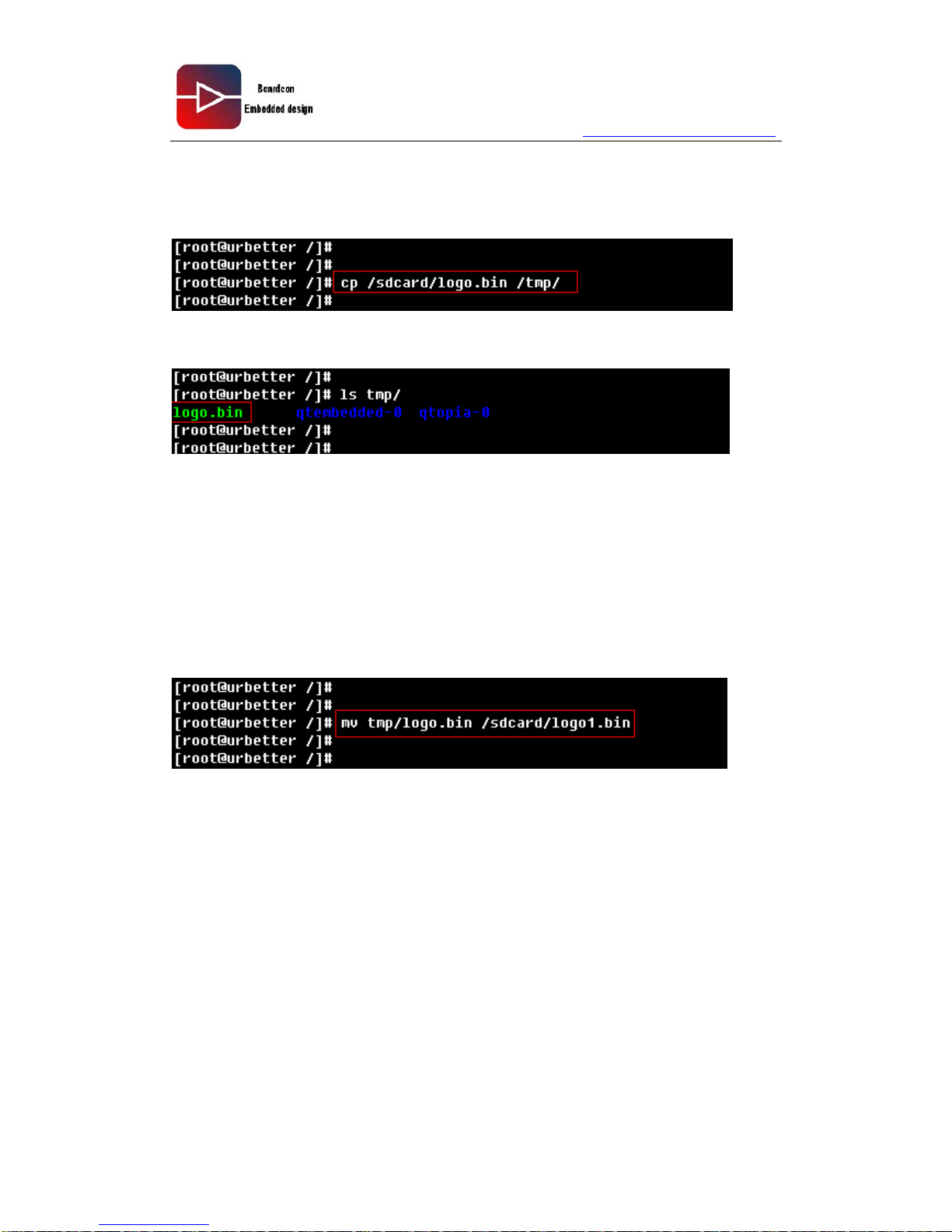
Inset the SD card into the SD card slot, here we inset a 2G Kingston card.
SD card will automatically mount to the sdcard directory which located in the root directory,
through the ls command, you can see the SD card has been successfully mounted
Unplug the SD card
Page 86
www.armdesigner.com
Android6410 Reference Guide
86
7.3.1. SD card Read Test
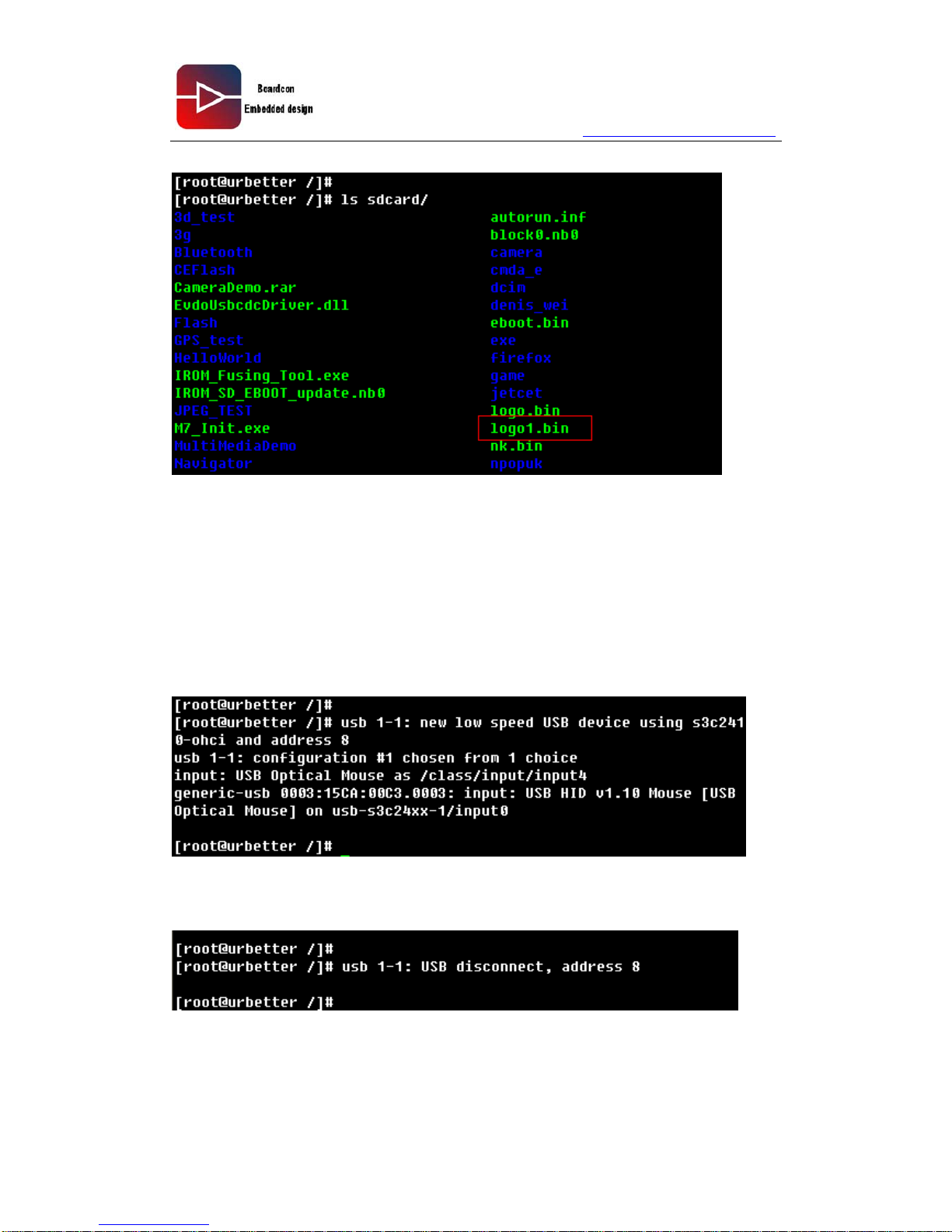
Download logo.bin which located in SD card to /tmp/
Use ls command to see the results
SD card read test is OK
7.3.2. SD card Write Test
Compile the tmp / logo.bin back to SD card, rename logo1.bin
Use mv command
Page 87
www.armdesigner.com
Android6410 Reference Guide
87
Use Is command to see the result
7.4. USB Test
The current version, support USB host functionality, USB OTG is not yet supported
7.4.1. USB Mouse Test
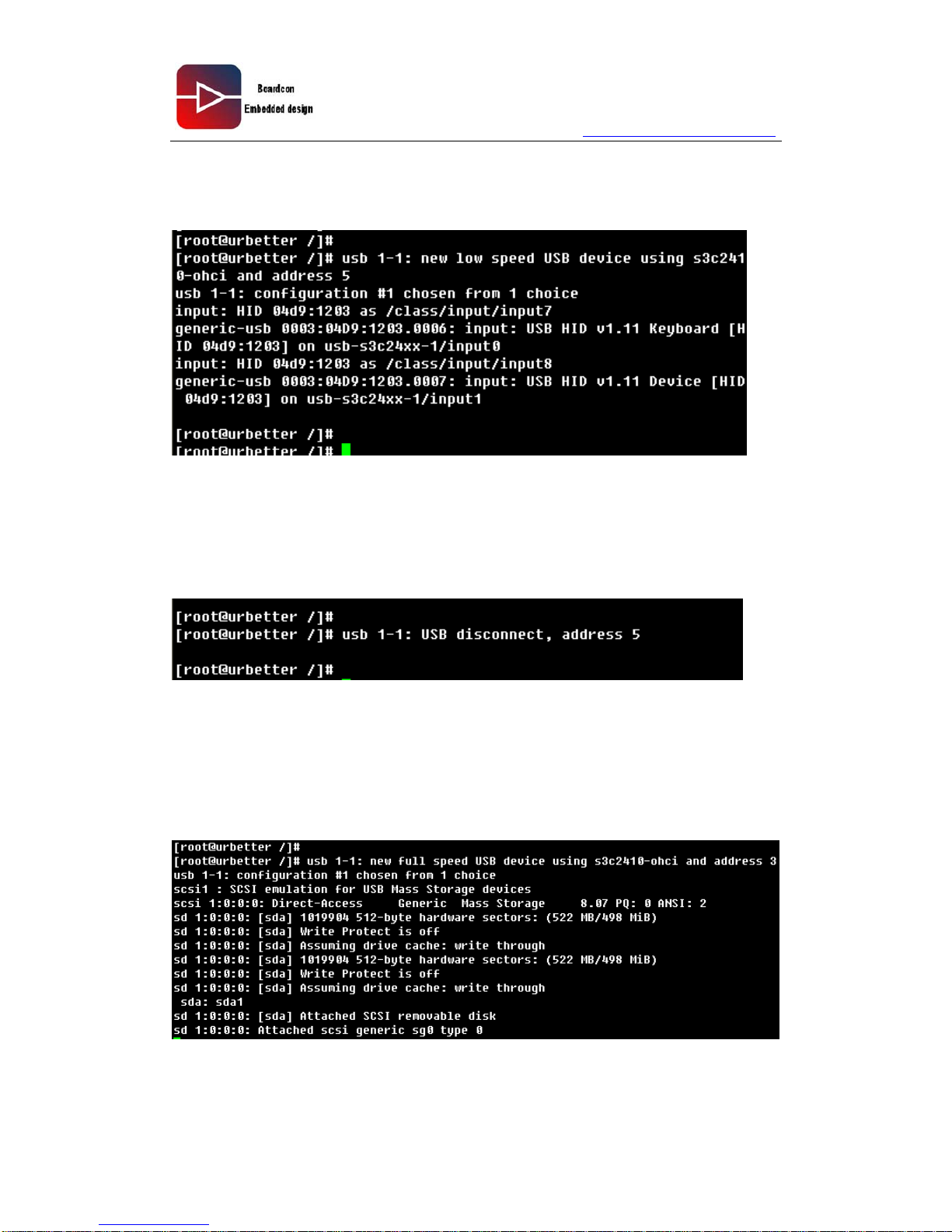
Inset USB mouse into the USB Host interface, the terminal will output information
Unplug the USB mouse
Page 88
www.armdesigner.com
Android6410 Reference Guide
88
7.4.2. USB Keyboard Test
Inset USB keyboard into the USB Host interface, the terminal will output information
Users can operate the keyboard function keys to test the keyboard, such as TAB key,
other users can open the QT on the terminal "Terminal", through the terminal to test the
reality of the functions of the keyboard.
Unplug the USB keyboard
7.4.3. U Disk Test
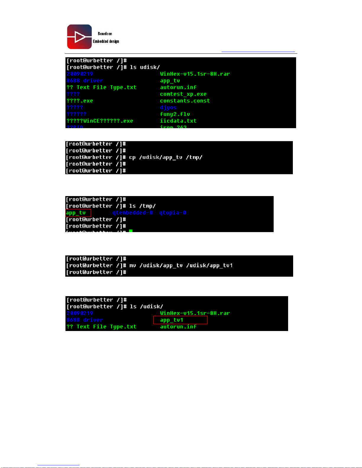
Inset U disk into the USB Host interface, the terminal will output information
U disk will automatically mount to / udisk, through the ls command to see udisk
Page 89
www.armdesigner.com
Android6410 Reference Guide
89
U disk read test: copy app_tv in U disk to / tmp
See the results through Is command
U disk write test: copy the / tmp / app_tv to U disk, named app_tv1
See the results through Is command
Page 90
www.armdesigner.com
Android6410 Reference Guide
90
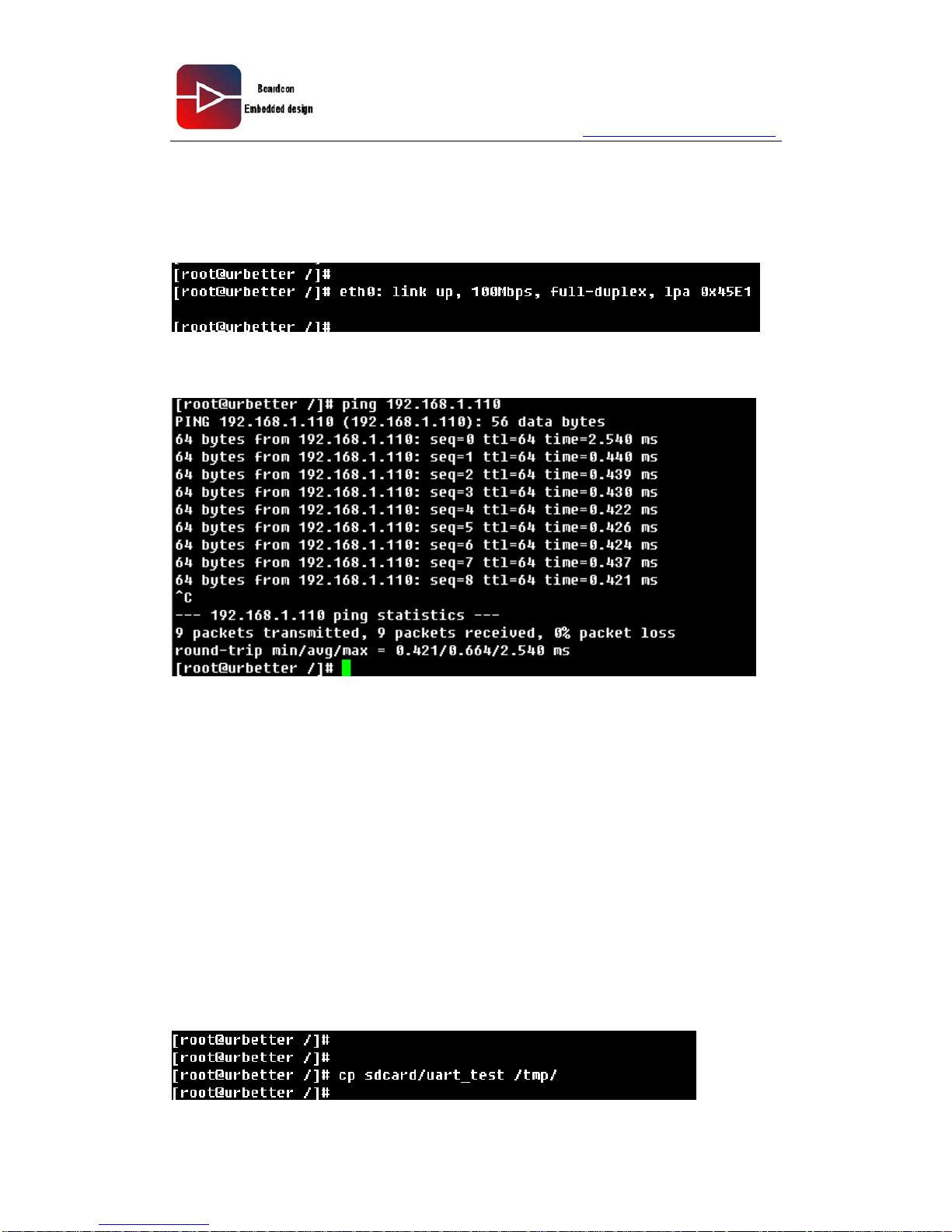
7.5. network port test
System is turned on, plug network cable
Single Board Computer ping host: ping 192.168.1.110
7.6. Serial Test
Following is the detailed steps to test the UART1, UART2, UART3 has the same testing
process
1. set SW2, let UART1 output from COM1
all the swi t c h e s of S W2 c o m e t o N O, t h at i s s e t ti ng S W 1 -8 t o 11111111
2. find another serial cable (cross, with the same serial line debugging), connected to
the Single Board Computer's COM1 through another one PC (a temporary name for
the test PC, windows xp system) COM port
3. copy \Test\linux test\UT_UART_test\ uart_test to SD card
4. inset SD card to Single Board Computer
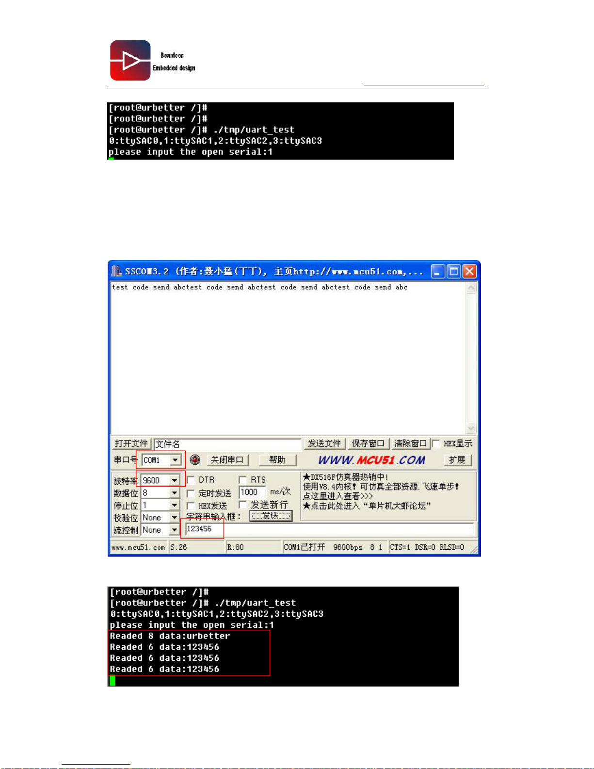
5. copy Serial port test program uart_test to /tmp from SD card
Page 91
www.armdesigner.com
Android6410 Reference Guide
91
6. Run directly tmp / uart_test, select the serial port test, where here option 1, Enter
7. copy test tool \Test\linux test\UT_UART_test\SSCOM32.EXE to test PC,run,here we
send the following things to Single Board Computer from test PC
Urbetter
123456
123456
123456
Single Board Computer terminal displays the received character
Page 92
www.armdesigner.com
Android6410 Reference Guide
92
After Single Board Computer receive character, sent "test code send abc" to the test
PC.From the above chart, we can see the test PC's serial debug terminal has received the
character Single Board Computer sent me.
7.7. Camera Test
Camera interface testing, please read Chapter VI 6.7,6.8,6.9 section.
7.8. Audio Test
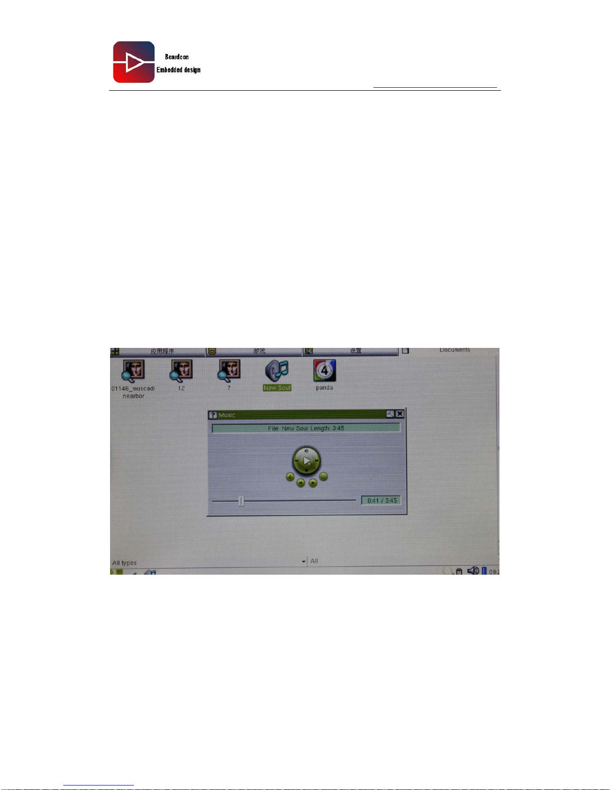
After system startup, plugged headphones or speakers into HEADPHONE interface, open
the QT interface of the "Documents" section
Double-click the interface directly to the MP3 test file: New Soul, the system will
automatically call the QT own audio player to play MP3.
Page 93
www.armdesigner.com
Android6410 Reference Guide
93
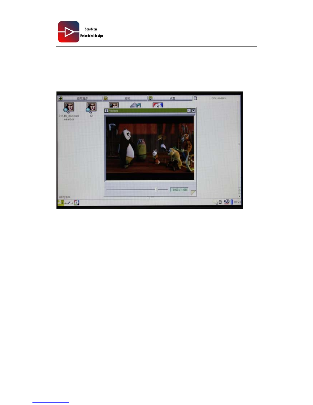
7.9. Video Test
Open the QT interface of the "Documents" section, double-click the video test file under
the interface panda, the system will automatically call the QT's own video player to play to
change the video.
7.10 Image View Test
Open the "Documents" section which is under QT interface , in the interface, we put three
JPEG images, double click the image, the system will automatically call the image viewer
to display images.
Page 94
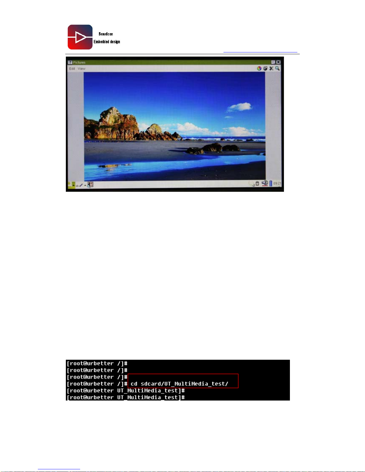
www.armdesigner.com
Android6410 Reference Guide
94
8. LINUX functional f multimedia
hardware coding
8.1. Run multimedia hardware codec test procedures
Before testing multimedia hardware codec, you should run the test program first, then test
the program by selecting the test items in test procedure
1、copy the whole \Test\linux test\UT_MultiMedia_test file to SDcard, UT_MultiMedia_test
file include test procedure UT_MultiMedia_test and video procedure(under TestVectors
file)
2. Inset the SD to the Single Board Computer,enter the UT_MultiMedia_test directory
through the terminal
Page 95
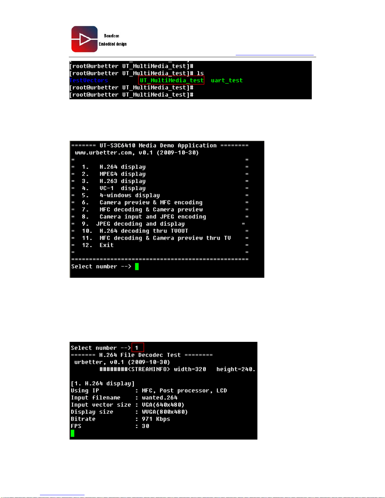
www.armdesigner.com
Android6410 Reference Guide
95
3、drive UT_MultiMedia_test test proccedure
# ./ UT_MultiMedia_test
8.2. H264 Video Hardware Decoding Test
Input 1,enter,start to test H264 hardware decoding test
Page 96
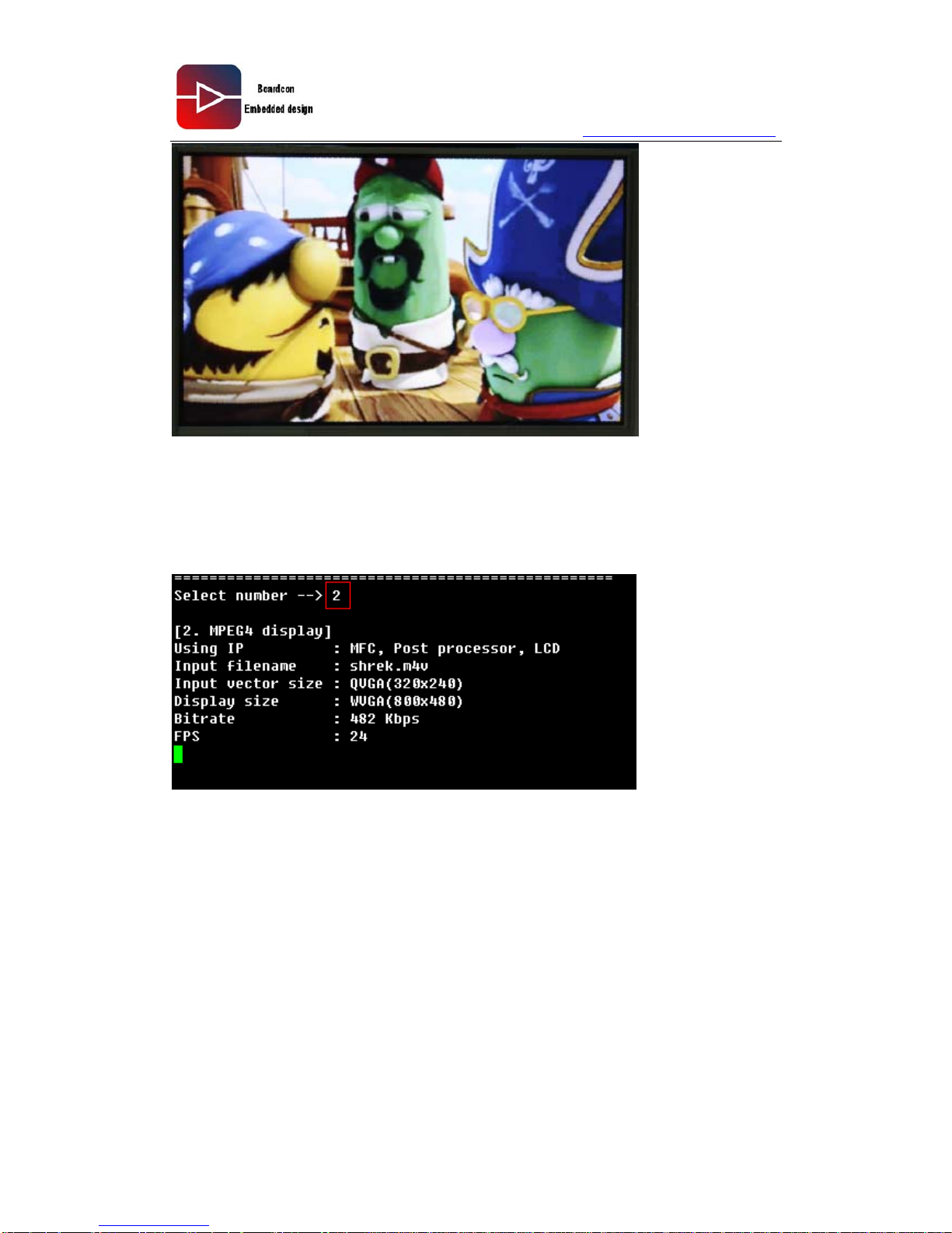
www.armdesigner.com
Android6410 Reference Guide
96
8.3. MPEG-4 Video Hardware Decoding Function Test
Input 2,enter start testing MPEG-4 hardware decoding function testing
Page 97
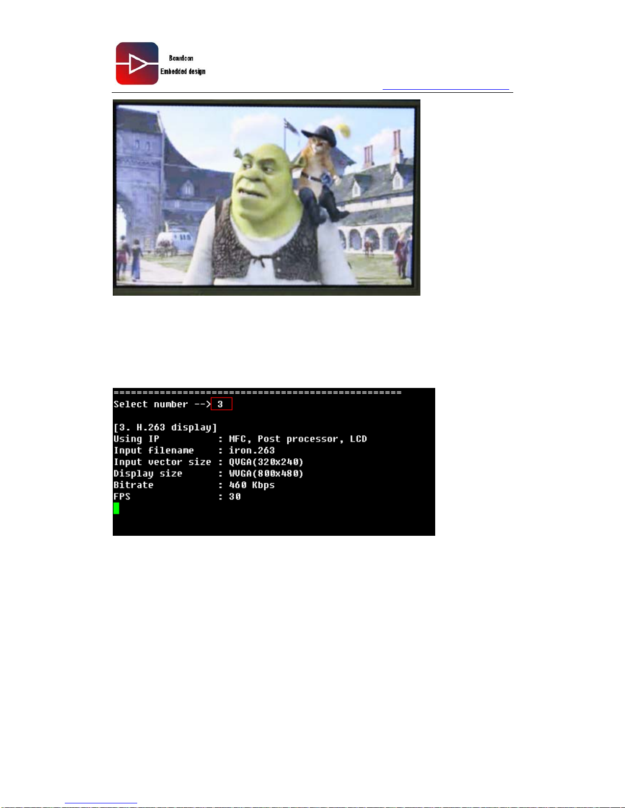
www.armdesigner.com
Android6410 Reference Guide
97
8.4. H263 Video Hardware Decoding Function Test
Input 3,enter,start testing H263 hardware decoding function testing
Page 98
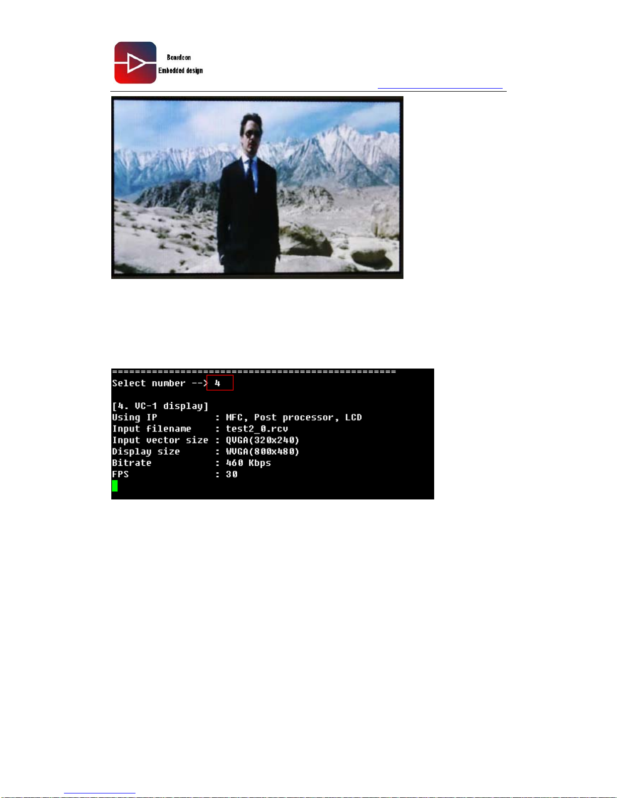
www.armdesigner.com
Android6410 Reference Guide
98
8.5. VC-1 Video Hardware Decoding Function Testing
Input 4,enter,start testing VC-1 hardware decoding function testing
Page 99

www.armdesigner.com
Android6410 Reference Guide
99
Page 100
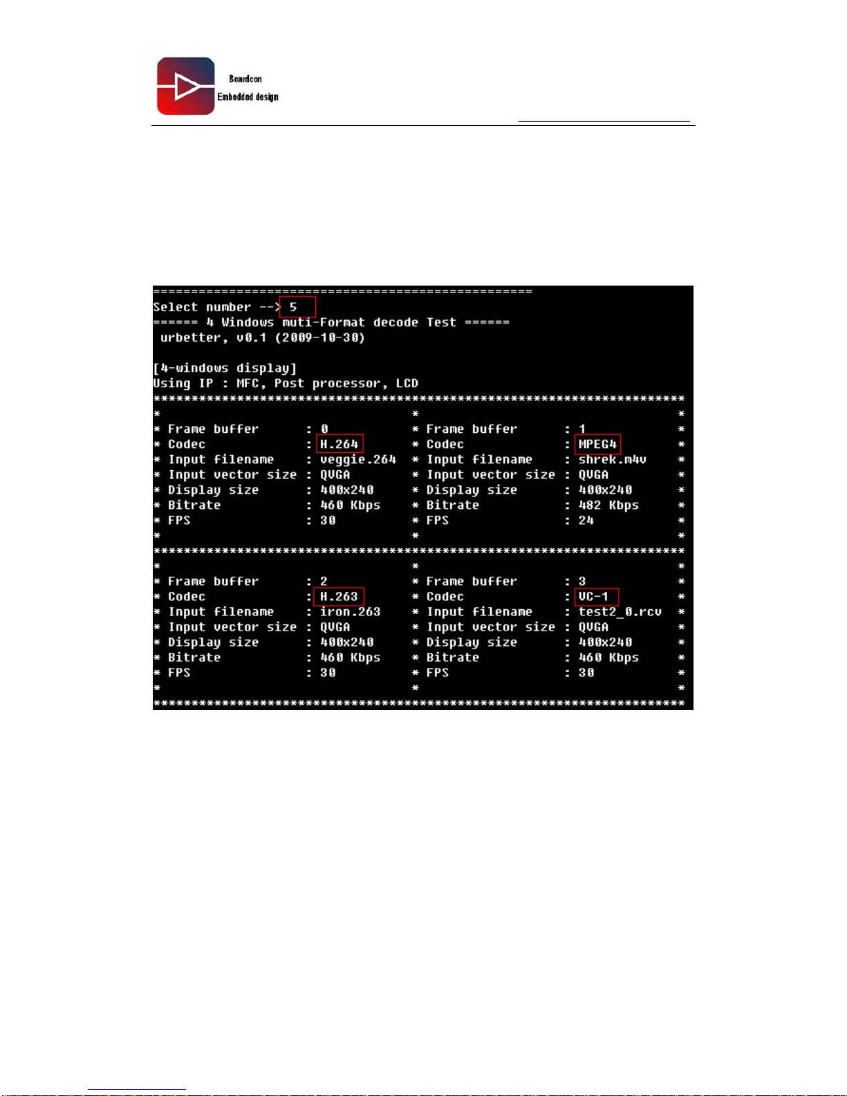
www.armdesigner.com
Android6410 Reference Guide
100
8.6. Multi-channel video test hardware decoding at the
same time
Input 5,enter
decoding hardware H264、MPEG4、H263、VC-1 at the same time in test4 window
 Loading...