


Android210 Hardware Manual
Boardcon Technology Limited
www.boardcon.com

www. boardcon.com
1
1. Introduction
1.1. About this Manual
This manual is intended to provide the user with an overview of the board and benefits, complete features
specifications, and set up procedures. It contains important safety information as well.
1.2. Feedback and Update to this Manual
To help our customers make the most of our products, we are continually making additional and updated
resources available on the Boardcon website (www.boardcon.com , www.armdesigner.com).
These include manuals, application notes, programming examples, and updated software and hardware.
Check in periodically to see what’s new!
When we are prioritizing work on these updated resources, feedback from customers is the number one
influence, if you have questions, comments, or concerns about your product or project, please no
hesitate to contact us at support@armdesigner.com.
1.3. Limited Warranty
Boardcon warrants this product to be free of defects in material and workmanship for a period of one year
from date of buy. During this warranty period Boardcon will repair or replace the defective unit in
accordance with the following process:
A copy of the original invoice must be included when returning the defective unit to Boardcon. This limited
warranty does not cover damages resulting from lighting or other power surges, misuse, abuse,
abnormal conditions of operation, or attempts to alter or modify the function of the product.
This warranty is limited to the repair or replacement of the defective unit .In no event shall Boardcon be
liable or responsible for any loss or damages, including but not limited to any lost profits, incidental or
consequential damages, loss of business, or anticipatory profits arising from the use or inability to use
this products.
Repairs make after the expiration of the warranty period are subject to a repair charge and the cost of
return shipping. Please contact Boardcon to arrange for any repair service and to obtain repair charge
information.

www. boardcon.com
2
Content
1 Android210 Introduction........................................................................................................................................ 3
1.1 Summary...................................................................................................................................................... 3
1.2 S5PV210AH Features................................................................................................................................ 3
1.3 Android210 Specifications......................................................................................................................... 4
1.4 PCB Dimension........................................................................................................................................... 5
1.5 Block Diagram............................................................................................................................................. 6
1.6 Motherboard Power meter.........................................................................................................................6
1.7 CPU Introduction.........................................................................................................................................7
2 Peripherals Introduction...................................................................................................................................... 10
2.1 Power (J1&J6)........................................................................................................................................... 10
2.2 Power switch (S1)..................................................................................................................................... 11
2.3 USB OTG (J2)........................................................................................................................................... 11
2.4 USB Host & USB HUB_SEL (J3, J41)...................................................................................................12
2.5 Ethernet (J35)............................................................................................................................................13
2.6 TVOUT (J28)............................................................................................................................................. 14
2.7 Audio I/O (J23, J24, J25, J26)................................................................................................................ 14
2.8 Serial ports (J9, J11, J14, J15)............................................................................................................... 15
2.9 SPI/AD (J29)..............................................................................................................................................17
2.10 Camera (J17, J21).................................................................................................................................. 18
2.11 GPIO/Keypad (J30, J31)........................................................................................................................20
2.12 GPIO/I2C (J5)..........................................................................................................................................21
2.13 Buttons (K1, K2, K3, RST).................................................................................................................... 21
2.14 Boot select (SW1)...................................................................................................................................22
2.15 LCD (J16, J18)........................................................................................................................................ 23
2.16 HDMI (J40).............................................................................................................................................. 24
2.17 WiFi (J19).................................................................................................................................................25
2.18 SD Card (J20)......................................................................................................................................... 25
2.19 RTC (BT1)................................................................................................................................................ 26
3 Product Configurations........................................................................................................................................27
3.1 Standard Contents....................................................................................................................................27
3.2 Optional Parts............................................................................................................................................27

www. boardcon.com
3
1 Android210 Introduction
1.1 Summary
Boardcon Android210 is an embedded computer based on a Samsung S5PV210AH-A0 at 1GHz ARM
Cortex-A8 CPU. An internal 64-bit bus provides a standard set of high-end on-board peripherals. The
Android210 features 512MB DDR2 and 512MB high-speed NAND flash. It is an ideal solution for
applications requiring cost-effective, low power and high performance.
To reduce total system cost and enhance overall functionality, Android210 allows development of
multi-function embedded applications through its multiple peripheral interfaces, which include 10/100
Ethernet port, USB HOST2.0, USB OTG2.0, serial ports, SD card socket, general I/O lines, RTC, audio
codec and speaker, touchscreen, and TFT 24-bit true color LCD interface.
Android210 runs Android 4.0 which uses an improved Linux 3.0 kernel (currently 3.0.8 version) that
allows bootup from NAND flash and provides driver support for all on-board hardware in a short time.
Equipped with the high-end processor, rich peripheral interface and open-source code, Android210 is
ideal for embedded applications such as arm pc, MID, Netbook, Learning machine, AD player, IPC, PDA,
GPS, Vehicle equipment, NVisual telephone, MMT, HMI, Monitoring equipment, and Teaching laboratory
equipment.
1.2 S5PV210AH Features
• ARM CortexTM-A8 based CPU Subsystem with NEON
− 32/ 32 KB I/D Cache, 512 KB L2 Cache
− Operating frequency up to 800 MHz or 1 GHz
• 64-bit Multi-layer bus architecture
− MSYS domain for ARM CortexTM-A8, 3D engine, Multi Format Codec and Interrupt Controller
• Operating frequency up to 200 MHz
− DSYS domain mainly for Display IPs (such as LCD controller, Camera interface, and TVout), and
MDMA
• Operating frequency up to 166 MHz
− PSYS domain mainly for other system component such as system peripherals, external memory
interface,
peri DMAs, connectivity IPs, and Audio interfaces.
• Operating frequency up to 133 MHz
− Audio domain for low power audio play
• Advanced power management for mobile applications
• 64 KB ROM for secure booting and 96 KB RAM for security function
• 8-bit ITU 601/656 Camera Interface supports horizontal size up to 4224 pixels for scaled and 8192
pixels for un-scaled resolution

www. boardcon.com
4
• Multi Format Codec provides encoding and decoding of MPEG-4/H.263/H.264 up to 1080p@30fps and
decoding of MPEG-2/VC1 video up to 1080p@30 fps
• 3D Graphics Acceleration with Programmable Shader up to 20M triangles/s and 1000 Mpixels/s
• 2D Graphics Acceleration up to 160Mpixels/s
• 1/ 2/ 4/ 8 bpp Palletized or 8/ 16/ 24 bpp Non-Palletized Color TFT recommend up to XGA resolution
• TV-out and HDMI interface support for NTSC and PAL mode with image enhancer
• MIPI-DSI and MIPI-CSI interface support
• One AC-97 audio codec interface and 3-channel PCM serial audio interface
• Three 24-bit I2S interface support
• One TX only S/PDIF interface support for digital audio
• Three I2C interface support
• Two SPI support
• Four UART supports three Mbps ports for Bluetooth 2.0
• On-chip USB 2.0 OTG supports high-speed (480 Mbps, on-chip transceiver)
• On-chip USB 2.0 Host support
• Asynchronous Modem Interface support
• Four SD/ SDIO/ HS-MMC interface support
• ATA/ ATAPI-6 standard interface support
1-3
S5PV210_UM 1 OVERVIEW OF S5PV210
• 24-channel DMA controller (8 channels for Memory-to-memory DMA, 16 channels for Peripheral DMA)
• Supports 14x8 key matrix
• 10-channel 12-bit multiplexed ADC
•Configurable GPIOs
• Real time clock, PLL, timer with PWM and watch dog timer
• System timer support for accurate tick time in power down mode (except sleep mode)
•Memory Subsystem
− Asynchronous SRAM/ ROM/ NOR Interface with x8 or x16 data bus
− NAND Interface with x8 data bus
− Muxed/ Demuxed OneNAND Interface with x16 data bus
− LPDDR1 Interface with x16 or x32 data bus (up to 400 Mbps/ pin DDR)
− DDR2 interface with x16 or x32 data bus (up to 400 Mbps/ pin DDR)
− LPDDR2 interface (up to 400 Mbps/ pin DDR)
1.3 Android210 Specifications
Feature
Specifications
CPU
Samsung S5PV210AH-A0, ARM Cortex-A8, up to 1GHz
Memory
512MB DDR2
NAND Flash
256MB/512MB/1GB optional
CPU Dimension
65.5mm x 52.8mm
Power Input
Two types of power supply: DC 12V@2A , Lithium cell

www. boardcon.com
5
USB
USB OTG 2.0, USB Host 2.0
Ethernet
10/100M Ethernet interface, DM9000
TVOUT
RCA, standard composite video signal output
COM
COM1, DB9 RS232 serial port;
COM1 ~ COM4 led out from a 20-pin expansion connector;
COM5 ~ COM6, RS485 serial port
SPI/AD
1-channel SPI interface, 2-channel ADC
Camera(optional)
2 Camera interfaces
GPIO/Keypad
GPIO / 8*8 matrix Keypad
Keys
1 Reset Key, 3 User Keys
LCD
4.3", 7" TTL/LVDS LCD
HDMI
HDMI v1.3, 1080p@30fps
WIFI(optional)
Two types of WIFI Module (SDIO interface and USB interface)
RTC Battery
External lithium battery
SD Card
Standard SD card interface
Carrier board Dimension
145mm x 115mm
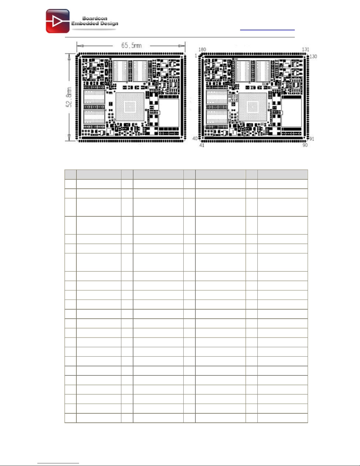
1.4 PCB Dimension

www. boardcon.com
6
1.5 Block Diagram
1.6 Motherboard Power meter
Support
voltage
12v/2A
System
Connected devices
Electric
current(A)
System
Connected devices
Electric
current(A)
Android
4.0
12v power
0.19
Android
4.0
Power, 7 inch
resistive screen
(TN92)
0.4
Android
4.0
Power, sd card, play video, U
disk, debug serial, Ethernet,
7inch LCD(TN92),
headphone, 2XSPEAKER
0.53
Android
4.0
SLEEP+7inch
LCD(TN92)
0.3
Linux
12v power
0.19
Linux
Power, 7 inch
Resistive
screen(TN92)
0.36
Linux
Power , SD card, play video,
U disk, debug serial,
Ethernet, 7inch LCD(TN92),
headphone,2XSPEAKER
0.45

www. boardcon.com
7
1.7 CPU Introduction
CM210-II is an embedded system on module used to design PDA with a Custom base board,
preinstalled Android4.0 OS. The module is designed to provide a cost-effective, low-power, high
performance Application Processor solution for MID, smartphone and so on.
Board Dimension
* Board size: 65.5mm x 52.8 mm x 3 mm
* Pin to Pin space: 1.27mm
* Stamp Hole: 1.5mm x 0.8mm
* Pin number: (J1A+J1C) x 40 + (J1B+J1D) x 50, total 180 pins
* Layer: 8 Layers, complying with EMS/EMI
Feature
* Power supply: 3.3V~ 5V
* The modular is led out most signals of S5PV210, such as 10/100 Ethernet port, USB HOST, USB OTG,
UART, GPIO, RTC, EXTINT, audio codec and speaker, HDMI and so on.
* Application: MID, smartphone, PDA, PND, automotive systems, data terminals, etc.
PCB Dimension
www. boardcon.com
8
Pin Definition
Pin
Signal
Pin
Signal
Pin
Signal
Pin
Signal
1
DC_IN
46
EINT17
91
EINT24
136
I2C_SCL1
2
DC_IN
47
EINT18
92
EINT25
137
DATA15
3
DC_IN
48
EINT19
93
AC97_SYNC/
i2sLRCK1
138
DATA14
4
VDD_IO
49
EINT20
94
AC97_BITCLK/
i2sSCLK1
139
DATA13
5
VDD_IO
50
EINT21
95
AC97_SDI/i2sSDI1
140
DATA12
6
VDD_ARM
51
HDMI_TX2N
96
AC97_SDO/i2sSDO1
141
DATA11
7
VDD_INT
52
HDMI_TX2P
97
AC97_RSTn/
i2sCDCLK1
142
DATA10
8
VDD_DDR2
53
HDMI_TX1N
98
EINT26
144
DATA9
9
VDD_RTC
54
HDMI_TX1P
99
EINT27
144
DATA8
10
GND55HDMI_TX0N
100
TXD3
145
DATA7
11
PWRRGTON
56
HDMI_TX0P
101
RXD3
146
DATA6
12
EINT9
57
HDMI_TXCN
102
TXD2
147
DATA5
13
OTG_ID
58
HDMI_TXCP
103
RXD2
148
DATA4
14
OTG_DP
59
VD0
104
RTSn1
149
DATA3
15
OTG_DM
60
VD1
105
CTSn1
150
DATA2
16
VBUS
61
VD2
106
TXD1
151
DATA1
17
OTG_DRVVBUS
62
VD3
107
RXD1
152
DATA0
18
HOST_DP
63
VD4
108
RTSn0
153
OEn
19
HOST_DN
64
VD5
109
CTSn0
154
Wen
20
EINT11
65
VD6
110
TXD0
155
CSn1
21
EINT12
66
VD7
111
RXD0
156
EINT10
22
MMC0_D0
67
VD8
112
SPI0_MOSI
157
ADDR2
23
MMC0_D1
68
VD9
113
SPI0_MISO
158
nRESET

www. boardcon.com
9
24
MMC0_D2
69
VD10
114
SPI0_CLK
159
EINT2
25
MMC0_D3
70
VD11
115
SPI0_CSn
160
OM5
26
MMC0_CLK
71
VD12
116
EINT28
161
OM3
27
MMC0_CMD
72
VD13
117
EINT29
162
OM2
28
MMC0_CDn
73
VD14
118
EINT30
163
OM1
29
EINT7
74
VD15
119
EINT31
164
EINT3
30
MMC1_D0
75
VD16
120
EINT0
165
EINT4
31
MMC1_D1
76
VD17
121
EINT1
166
EINT5
32
MMC1_D2
77
VD18
122
CAM_D7
167
KEY_RST
33
MMC1_D3
78
VD19
123
CAM_D6
168
EINT6
34
MMC1_CLK
79
VD20
124
CAM_D5
169
ADCIN1
35
MMC1_CMD
80
VD21
125
CAM_D4
170
ADCIN0
36
MMC1_CDn
81
VD22
126
CAM_D3
171
GND
37
EINT8
82
VD23
127
CAM_D2
172
GND
38
EINT13
83
VSYNC
128
CAM_D1
173
GND
39
EINT14
84
HSYNC
129
CAM_D0
174
GND
40
EINT15
85
VCLK
130
CAM_PCLK
175
GND
41
TSXM1
86
VDEN
131
CAM_CLKOUT
176
GND
42
TSXP1
87
PWMTOUT0
132
CAM_VSYNC
177
GND
43
TSYM1
88
EINT22
133
CAM_HREF
178
GND
44
TSYP1
89
EINT23
134
CAM_FIELD
179
GND
45
EINT16
90
DAC_OUT0
135
I2C_SDA1
180
GND

www. boardcon.com
10
2 Peripherals Introduction
2.1 Power (J1&J6)
Android210 supports two types of power input.
1. Power supply: DC 12V/2A
J1
Pin
Signal
Description
Pin
Signal
Description
1
12V_IN
DC12V. Power in
2
GND
Ground

www. boardcon.com
11
3
GND
Ground
2. Lithium-ion polymer battery 7.4V (Default not solder)
J6
Pin
Signal
Description
Pin
Signal
Description
1
VBAT
Connect to EUP8057
2
GND
Ground
2.2 Power switch (S1)
The power switch is a toggle switch, controlling the evaluation board power ON/OFF.
Pin
Signal
Description
Pin
Signal
Description
1
VDD_IN
DC12V. Power in
2
VDD_IN
DC12V. Connect to FUSE
3NCNot connect
4NCNot connect
5NCNot connect
6NCNot connect
7NCNot connect
8NCNot connect
2.3 USB OTG (J2)
HS OTG can be configured as a Host-only or Device-only controller. Default is Device-only controller. It is
used to download image.
Features:
• Supports USB 2.0 High Speed (480Mbps), Full Speed (12Mbps) and Low Speed (1.5Mbps) operation
in host mode
• Supports USB 2.0 High Speed (480 Mbps) and Full Speed (12 Mbps) operation in device mode.
• Hardware support: OTG signaling, session request protocol, and host negotiation protocol

www. boardcon.com
12
Pin
Signal
Description
Pin
Signal
Description
1
VBUS
USB OTG
mini-Receptacle Vbus
2
OTG_DM
USB OTG negative
data
3
OTG_DP
USB OTG positive
data
4
OTG_ID
USB OTG ID signal
5
GND
Ground
6
GND
Ground
7
GND
Ground
8
GND
Ground
9
GND
Ground
2.4 USB Host & USB HUB_SEL (J3, J41)
The Android 210 only supports a A –type USB host 2.0 at High Speed (480Mbps), Full Speed (12Mbps)
and Low Speed (1.5Mbps) modes. It is used to connect USB mouse, U disk and other USB devices.
Hot-plug is supported.
USB Host (J3)
Pin
Signal
Description
Pin
Signal
Description
1
VDD_5V
5V voltage
2
USBDNA
USB host port A negative data
3
USBDPA
USB host port A positive data
4
GND
Ground
5
GND
Ground
6
GND
Ground
7
GND
Ground
8
GND
Ground

www. boardcon.com
13
J41 is used to select USB HUB (effect on Host). Connect Pin3&5, Pin4&6 with Jumper is select USB
HUB, USB host is available; and connect Pin1&3, Pin2&4 is not.
USB HUB Select (J41)
Pin
Signal
Description
Pin
Signal
Description
1
USBDPA
USB host positive data A
2
USBDNA
USB host negative data A
3
HOST_DP
USB host positive data
4
HOST_DN
USB host negative data
5
USBDPU
USB host positive data use
6
USBDNU
USB host negative data use
2.5 Ethernet (J35)
Android 210 incorporates a full-featured 10/100M Ethernet interface. The platform adopts DM9000AEP
as the Ethernet chip.
Features:
• 10/100 BASE-T IEEE 802.3 compliant
• IEEE 802.3u compliant Auto-Negotiation
• Integrated IEEE 1588 time stamping module (inside the MAC).
• Automatic channel swap (ACS)
• Full- and Half-duplex
• Automatic MDI/MDIX crossover
• Automatic polarity correction
• Activity and speed indicator LED controls
• You can set a fixed IP or automatically obtain IP
Pin
Signal
Description
Pin
Signal
Description
1
DM9000_TX+
Net data send +
2
DM9000_TX-
Net data send -
3
DM9000_RX+
Net data receive +
4
NET_AVDD25
Connect to
DM9000AEP
5
NET_AVDD25
Connect to
DM9000AEP
6
DM9000_RX-
Net data receive 7NCNot connect
8
GND
Ground
9
VDD_IO
IO Supply Voltage
(3.3V Power in )
10
DM9000_LINKLED
Detect link

www. boardcon.com
14
11
DM9000_LANLE
D
LANLED detect speed
12
VDD_IO
IO Supply Voltage
(3.3V Power in )
2.6 TVOUT (J28)
S5PV210 MCU comes with 1 TVOUT, standard composite video signal, can be connected to all kinds of
video device directly.
Note: The TVOUT driver is unavailable.
Pin
Signal
Description
Pin
Signal
Description
1
DAC_OUT0
Analog output of Video DAC
2
GND
Ground
2.7 Audio I/O (J23, J24, J25, J26)
The development board adopts IIS chip WM8976G, supports stereo audio output (Green, 3.5mm audio
jack) and MIC recording (Pink 33.5mm audio jack).
Features:
Low power
Integrated ADC and DAC
IIS transfer audio data
Stereo output, support recording
Note: The recording driver is unavailable.
MIC
Pin
Signal
Description
Pin
Signal
Description
1
MICIN
MIC input
2
MICIN
MIC input
3
MICIN
MIC input
4
MICIN
MIC input
5
GND
Ground
www. boardcon.com
15
PHONE
Pin
Signal
Description
Pin
Signal
Description
1
HPL
Left Channel Headphone Output
2
HPL
Left Channel Headphone Output
3
HPR
Right Channel Headphone
Output
4
HPR
Right Channel Headphone Output
5
GND
Ground
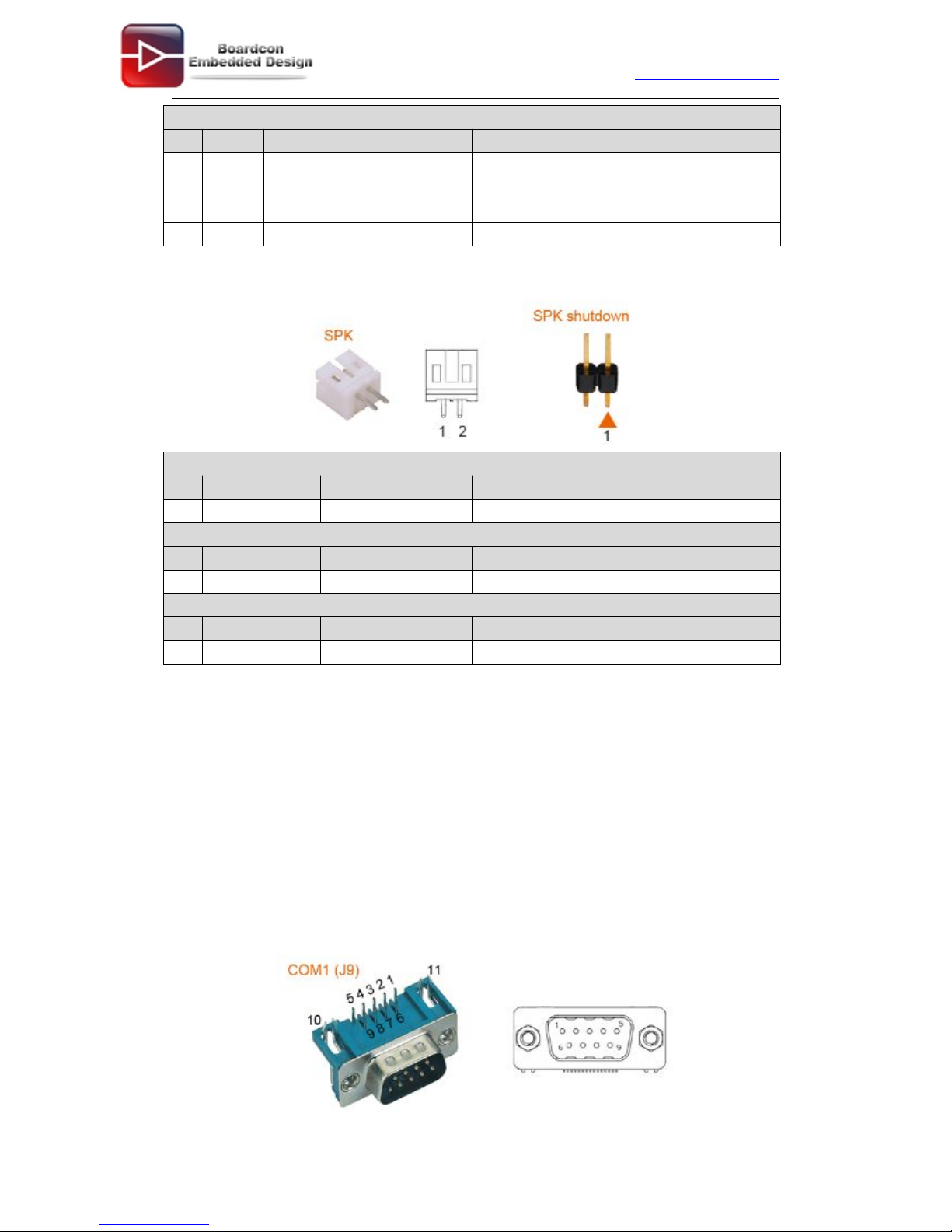
Android 210 supports 2-chanel SPEAKER that led out from 2x 2-pin 2.0mm connectors. The SPK on/off
is controlled by a 2-pin 2.0mm connector (J27). Connect J27 with jumper is shutdown the SPKs.
SPKL (J25)
Pin
Signal
Description
Pin
Signal
Description
1
VOUT1L
Output 1 left channel
2
VOUT2L
Output 2 left channel
SPKR(J26)
Pin
Signal
Description
Pin
Signal
Description
1
VOUT1R
Output 1 right channel
2
VOUT2R
Output 2 right channel
SPK Shutdown(J27)
Pin
Signal
Description
Pin
Signal
Description
1
SHUTDOWN
SHUTDOWN speaker
2
GND
Ground
2.8 Serial ports (J9, J11, J14, J15)
Android 210 supports 1x RS232 (DB9), 4x TTL (or 2x TTL and 2x RS485).
Features:
• 32-entry FIFO for receiver and 32-entry FIFO for transmitter
• Programmable baud rate of up to 250K bit/s
• The serial port operates at RS232 voltage levels.
The COM1 is debug serial port. It is used to input and display interactive command, view system boot
information and transfer files between the platform and PC.

www. boardcon.com
16
COM1 (J9)
Pin
Signal
Description
Pin
Signal
Description
1NCNot connect
2
RXD0N
Uart 0 receives data input
3
TXD0N
Uart 0 transmits data output
4NCNot connect
5
GND
Ground
6NCNot connect
7
CTSn0N
Uart 0 clean to send input
signal
8
RTSn0N
Uart 0 request to send output
signal
9NCNot connect
10
GND
Ground
11
GND
Ground
The UART (J11) is a 20-pin connector and can be extended to 4x serial ports (TTL). The serial signals
are led out directly from CPU.
The signal TXD0/RXD0 shared with COM1 (DB9). If it is used as debug, TXD0/RXD0 in UART is disabled.
The UART is use to connect serial device.
The signals TXD2/RXD2 and TXD3/RXD3 shared with COM5 and COM6.
COM1/2/3/4 (J11)
Pin
Signal
Description
Pin
Signal
Description
1
VDD_5V
5V voltage
2
VDD_IO
IO Supply Voltage
3
TXD0
Uart 0 transmits data output
4
RXD0
Uart 0 receives data input
5
RTSn0
Uart 0 request to send output
signal
6
CTSn0
Uart 0 clean to send input
signal
7
TXD1
Uart 1 transmits data output
8
RXD1
Uart 1 receives data input
9
RTSn1
Uart 1 request to send output
signal
10
CTSn1
Uart 1 clean to send input
signal
11
TXD2
Uart 2 transmits data output
12
RXD2
Uart 2 receives data input
13
TXD3
Uart 3 transmits data output
14
RXD3
Uart 3 receives data input
15NCNot connect
16NCNot connect
17NCNot connect
18NCNot connect
19
GND
Ground
20
GND
Ground
RS485 uses differential mode to transmit signals, without checking the signal just check potential
difference to send / receiver data.
COM5 and COM6 are converted by COM3 (TXD2/RXD2) and COM4 (TXD3/RXD3).

www. boardcon.com
17
Features:
• 9-bit or Multidrop mode (RS-485) support (automatic slave address detection);
• RXD input and TXD output can be inverted respectively in RS-485 mode;
• RS-485 driver direction control via CTS signal.
COM5 (J14)
Pin
Signal
Description
Pin
Signal
Description
1BConnect to MAX3430(inverting
terminal)
2AConnect to
MAX3430(non-inverting terminal)
COM6 (J15)
Pin
Signal
Description
Pin
Signal
Description
1BConnect to MAX3430(inverting
terminal)
2AConnect to
MAX3430(non-inverting terminal)
2.9 SPI/AD (J29)
Android210 reserves 1- channel high-speed SPI and 2- channel ADC interface.
SPI features:
• Full duplex
• 8/16/32-bit shift register for TX/RX
• 8-bit Prescaler logic
• 2 clock sources: PCLK and SPI_EXT_CLK from SYSCON
• Supports 8-bit/16-bit/32-bit bus interface
• Supports the Motorola SPI protocol and National Semiconductor Microwire
• Two independent 32-bits wide transmit and receive FIFOs: depth 64 in port 0 and depth 16 in port 1
• Master-mode and Slave-mode
• Receive-without-transmit operation
• Tx/Rx maximum frequency at up to 50MHz
www. boardcon.com
18
Pin
Signal
Description
Pin
Signal
Description
1
VDD_5V
5V Voltage
2
VDD_IO
IO Supply Voltage
3
SPI0_CSn
SPI CH0 chip select
4
SPI0_MISO
SPI CH0 master input
/ slave output
5
SPI0_CLK
SPI CH0 clock
6
SPI0_MOSI
SPI CH0 master
output / slave input
7NCNot connect
8NCNot connect
9NCNot connect
10NCNot connect
11NCNot connect
12NCNot connect
13NCNot connect
14NCNot connect
15NCNot connect
16NCNot connect
17
ADC_IN0
12bit ADC CH0 input
18
ADC_IN1
12bit ADC CH1 input
19
GND
Ground
20
GND
Ground
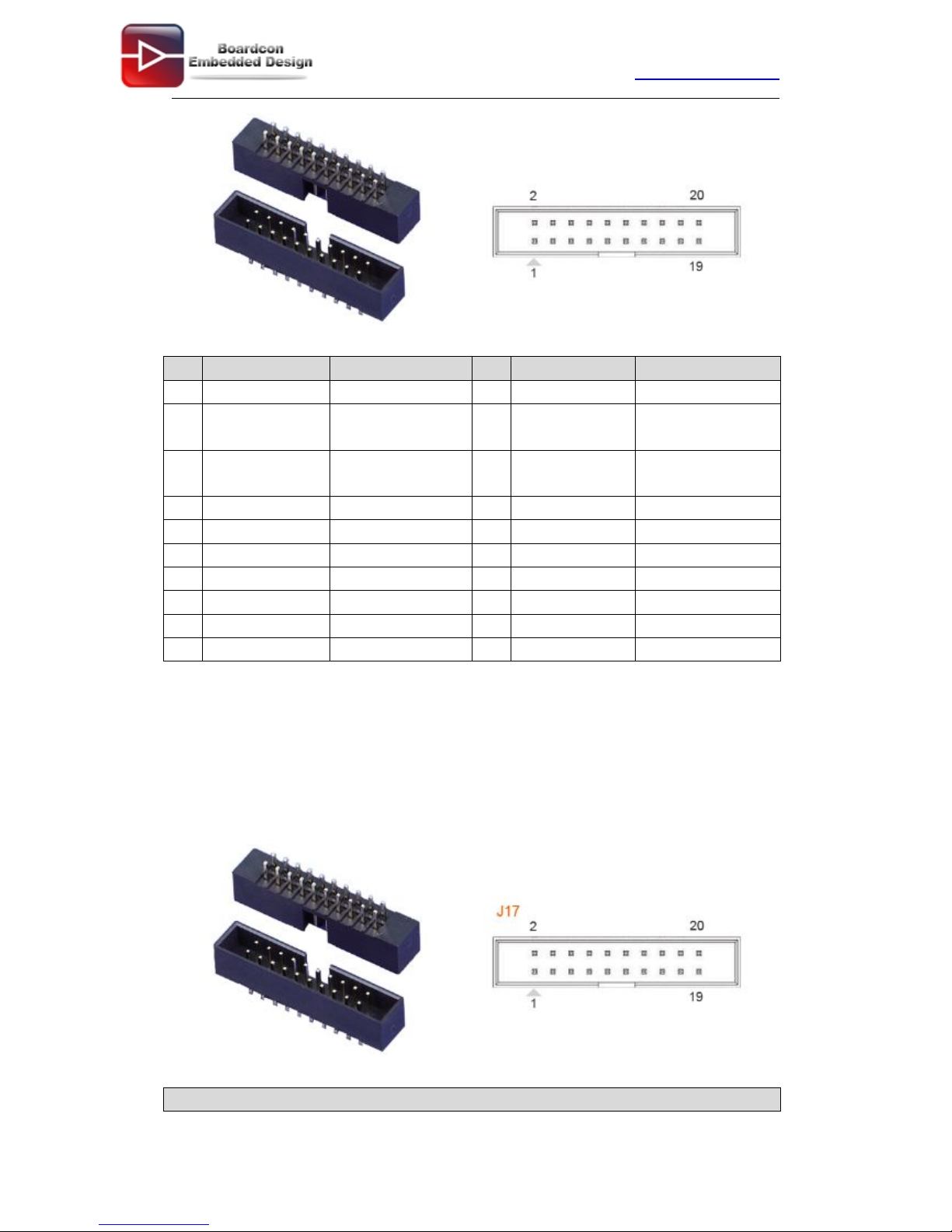
2.10 Camera (J17, J21)
Android210 provides 2 types of camera interfaces: header and FPC connector.
J17 is a 2mm pitch 20-pin header connector. It can be connected to the 1.3M pixels OV9650 module
combined with an adapter plate.
J17

www. boardcon.com
19
Pin
Signal
Description
Pin
Signal
Description
1
VDD_5V
5V Voltage
2
VDD_IO
IO Supply Voltage
3
GND
Ground
4
CAMFIELD
Reset or Power down
Camera
5
LCAMPCLK
Camera clock in
6
CAM_SCL
Camera IIC-bus CH
clock
7
CAM_SDA
Camera IIC-bus CH data
8
LCAMVSY NC
Camera VSYNC in
9
LCAMHREF
Camera HSYNC in
10
LCAMCLK
Master clock
11
LCAMDATA0
Camera data 0 in
12
LCAMDATA1
Camera data 1 in
13
LCAMDATA2
Camera data 2 in
14
LCAMDATA3
Camera data 3 in
15
LCAMDATA4
Camera data 4 in
16
LCAMDATA5
Camera data 5 in
17
LCAMDATA6
Camera data 6 in
18
LCAMDATA7
Camera data 7 in
19
GND
Ground
20
GND
Ground
J21 is a 24pin FPC connector. It can be connected directly to camera module without any adapter plate.
J21
Pin
Signal
Description
Pin
Signal
Description
1
EINT22
Interrupt port 22
2
GND
Ground
3
CAM_SDA
Camera IIC-bus CH
data
4
CAM_2.8V
2.8V Voltage for
camera
5
CAM_SCL
Camera IIC-bus CH
clock
6
CAMFIELD
Reset or Power down
Camera
7
LCAMVSY NC
Camera VSYNC in
8
EINT21
Interrupt port 21
9
LCAMHREF
Camera HSYNC in
10
CAM_1.8V
1.8V Voltage for
camera
11
CAM_2.8V
2.8V Voltage for
camera
12
LCAMDATA7
Camera data 7 in
13
LCAMCLK
Master clock
14
LCAMDATA6
Camera data 6 in
15
GND
Ground
16
LCAMDATA5
Camera data 5 in
17
LCAMPCLK
Camera clock in
18
LCAMDATA4
Camera data 4 in
19
LCAMDATA0
Camera data 0 in
20
LCAMDATA3
Camera data 3 in
21
LCAMDATA1
Camera data 1 in
22
LCAMDATA2
Camera data 2 in
23NCNot connect
24NCNot connect

www. boardcon.com
20
2.11 GPIO/Keypad (J30, J31)
J30 is a 20-Pin 2.0 connector multiplexed GPIO and Keypad.
Keypad Features:
• Open drain design
• Glitch suppression circuit design
• Multiple-key detection
• Long key-press detection
• Support 2-point and 3-point contact key matrix
J31 is GPIO interface that can connect a variety of external devices. The pins can be defined as:
• Data input / output.
• Interrupt generation.
GPIO/8*8 Keypad (J30)
Pin
Signal
Description
Pin
Signal
Description
1
VDD_5V
5V Voltage
2
VDD_IO
IO Supply Voltage
3
EINT24
Interrupt 24 (OR KP_ROW0 )
4
EINT25
Interrupt 25(OR KP_ROW1)
5
EINT26
Interrupt 26(OR KP_ROW2 )
6
EINT27
Interrupt 27(OR KP_ROW3 )
7
EINT28
Interrupt 28(OR KP_ROW4)
8
EINT29
Interrupt 29(OR KP_ROW5)
9
EINT30
Interrupt 30(OR KP_ROW6)
10
EINT31
Interrupt 31(OR KP_ROW7)
11
EINT16
Interrupt 16(OR KP_COL0 )
12
EINT17
Interrupt 17(OR KP_COL1)
13
EINT18
Interrupt 18(OR KP_COL2)
14
EINT19
Interrupt 19(OR KP_COL3)
15
EINT20
Interrupt 20(OR KP_COL4 )
16
EINT21
Interrupt 21(OR KP_COL5)
17
EINT22
Interrupt 22(OR KP_COL6)
18
EINT23
Interrupt 23(OR KP_COL7 )
19
GND
Ground
20
GND
Ground
GPIO (J31)
Pin
Signal
Description
Pin
Signal
Description
1
VDD_5V
5V Voltage
2
VDD_IO
IO Supply Voltage
3
EINT0
Interrupt 0
4
EINT1
Interrupt 1
5
EINT2
Interrupt 2
6
EINT3
Interrupt 3
7
EINT4
Interrupt 4
8
EINT5
Interrupt 5
9
EINT6
Interrupt 6
10
MMC0_WP/
MMC0 WP/Interrupt 7
www. boardcon.com
21
EINT7
11
EINT8
Interrupt 8
12
EINT9
Interrupt 9
13
EINT10
Interrupt 10
14
EINT11
Interrupt 11
15
EINT12
Interrupt 12
16
HDMI_INT/
EINT13
Defined for HDMI HPD
signal /Interrupt 13
17
EINT14
Interrupt 14
18
EINT15
Interrupt 15
19
GND
Ground
20
GND
Ground
2.12 GPIO/I2C (J5)
The J5 connector is used to connect the capacitive touchscreen.
Pin
Signal
Description
Pin
Signal
Description
1
VDD_IO
IO Supply Voltage
2
EINT5
Interrupt 5
3
EINT15
Interrupt 15
4
I2C_SCL1
I2C clock signal
5
I2C_SDA1
I2C data signal
6
GND
Ground
7
KP_COL0
Keypad col0
8
KP_COL1
Keypad col1
9
KP_COL2
Keypad col2
10
EINT24
Interrupt 24
11
EINT25
Interrupt 25
12
EINT26
Interrupt 26
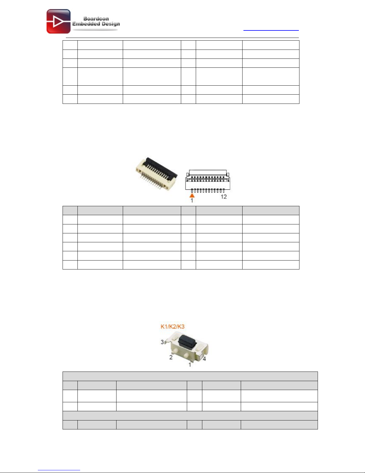
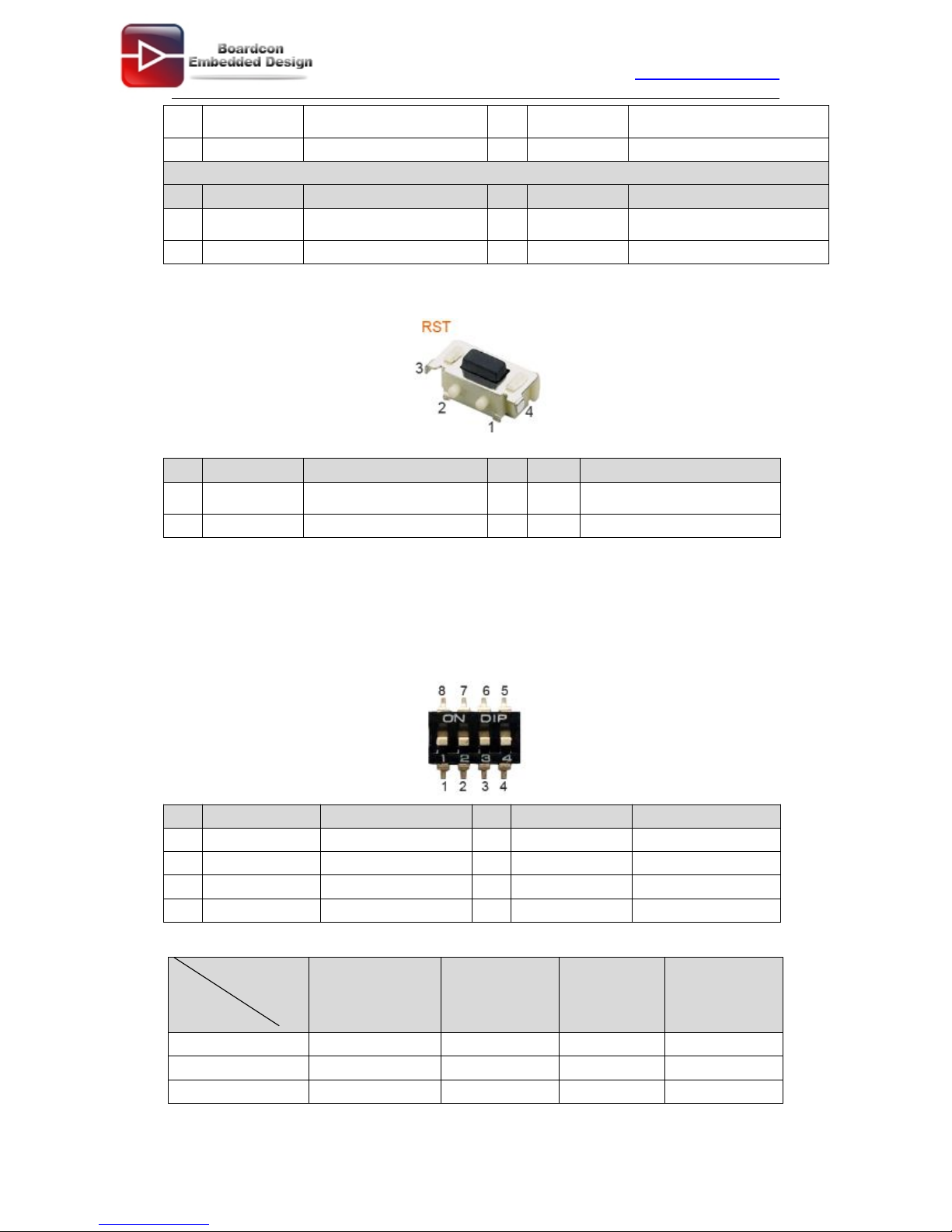
2.13 Buttons (K1, K2, K3, RST)
On-board 3x user buttons (User-Defined) and 1 reset button.
K1
Pin
Signal
Description
Pin
Signal
Description
1
VDD_IO
IO Supply Voltage
2
EINT24
Interrupt 24
3
GND
Ground
4
GND
Ground
K2
Pin
Signal
Description
Pin
Signal
Description
www. boardcon.com
22
1
VDD_IO
IO Supply Voltage
2
EINT25
Interrupt 25
3
GND
Ground
4
GND
Ground
K3
Pin
Signal
Description
Pin
Signal
Description
1
VDD_IO
IO Supply Voltage
2
EINT26
Interrupt 26
3
GND
Ground
4
GND
Ground
The RST button is a Side Tact Switch. The board adopts MAX811 as the Reset chip.
Pin
Signal
Description
Pin
Signal
Description
1
KEY_RST
Connect to pin3 of MAX811
2
GND
Ground
3
GND
Ground
4
GND
Ground
2.14 Boot select (SW1)
Android210 supports booting from SD Card, USB and NAND Flash. The CPU will boot in
corresponding way automatically after getting the OM signal set by DIP switch SW1.
Pin
Signal
Description
Pin
Signal
Description
1
VDD_IO
IO Supply Voltage
2
VDD_IO
IO Supply Voltage
3
VDD_IO
IO Supply Voltage
4
VDD_IO
IO Supply Voltage
5
OM5
Mode selection 5
6
OM3
Mode selection 3
7
OM2
Mode selection 2
8
OM1
Mode selection 1
Boot mode
Boot mode
J1J2J3
J4
NAND FLASH
100
0
USB1001
SD card0110
Pin

www. boardcon.com
23
NOTE: 1. Android210 is set to boot from NAND Flash by default.
2. For SW1 switch, “1”= ON, “0” = OFF.
2.15 LCD (J16, J18)
Android210 supports two types of LCD interfaces, one is 40P FPC and the other is 50P header.
The board comes with driver for 4.3-inch resistive, 7-inch resistive/capacitive LCD. User also can choose
other size of LCD&touchscreen. Android210 supports 24bit LCD, PWM backlight and external interrupt
control.
J16 (50P)
Pin
Signal
Pin
Signal
Pin
Signal
Pin
Signal
1
VDD_5V
2
VDD_5V
3
VDD_IO
4
GND
5NC6
VD07VD18VD2
9
VD310VD411VD512VD6
13
VD714VD815VD916VD10
17
VD11
18
GND19VD12
20
VD13
21
VD14
22
VD15
23
VD16
24
VD17
25
VD18
26
VD19
27
VD20
28
VD21
29
VD22
30
VD23
31
GND32NC
33
PWMTOUT0
34NC35NC36
DE
37
VSY NC
38
HSY NC
39
VCLK
40
NC
41NC42
GND43XM44XP
45NC46
GND47YM48YP
49NC50
GND
J18 (40P)
Pin
Signal
Pin
Signal
Pin
Signal
Pin
Signal
www. boardcon.com
24
1
VDD_5V
2
VDD_5V
3
VDD_IO
4
VD0
5
VD16VD27VD38VD4
9
VD510VD611VD712VD8
13
VD914VD10
15
VD11
16
VD12
17
VD13
18
VD14
19
VD15
20
VD16
21
VD17
22
VD18
23
VD19
24
VD20
25
VD21
26
VD22
27
VD23
28
NC
29
PWMTOUT0
30DE31
VSY NC
32
HSY NC
33
VCLK
34NC35XM36
XP
37YM38YP39
GND40GND
2.16 HDMI (J40)
Android210 supports HDMI v1.3,1080p@30fps at 60Hz high-definition digital output, and it also enables
HDMI/LCD audio and video synchronization output. The HDMI interface is the regular 19pins HDMI type
A, with width 13.9mm and thickness 4.45mm.
Pin
Signal
Description
Pin
Signal
Description
1
HDMI_TX2P
HDMI phy transmits data
output 2 P
2
GND
Ground
3
HDMI_TX2N
HDMI phy transmits data
output 2 N
4
HDMI_TX1P
HDMI phy transmits
data output 1 P
5
GND
Ground
6
HDMI_TX1N
HDMI phy transmits
data output 1 N
7
HDMI_TX0P
HDMI phy transmits data
output 0 P
8
GND
Ground
9
HDMI_TX0N
HDMI phy transmits data
output 0 N
10
HDMI_TXCP
HDMI phy TX clock P
11
GND
Ground
12
HDMI_TXCN
HDMI phy TX clock N
13
GND
Ground
14NCNot connect
15
HDMI_SCL1
HDMI clock signal 1
16
HDMI_SDA1
HDMI data signal 1
17
GND
Ground
18
VDD_5V
5V Voltage
19
HDMI_INT/
EINT13
HDMI interrupt /interrupt 13
20
GND
Ground
21
GND
Ground
22
GND
Ground

www. boardcon.com
25
23
GND
Ground
2.17 WiFi (J19)
J19 is SDIO WIFI wireless network interface (MMC CH1).
Note: The signals USB DNB / USB DPB are reserved for USB WIFI module.
Features:
WLAN Standards: IEEE 802 Part 11b/g (802.11b/g)
Coexistence: Hardware signaling
Frequency Band: 2.400 ~ 2.484 GHz
Pin
Signal
Description
Pin
Signal
Description
1NCNot connect
2
SD1_VDD
SD1 Voltage
3
SDCH1_DATA1/
MMC1_D1
SDCH1 interface
DATA1/MMC1 DATA1
4
SD1_VDD
SD1 Voltage
5
SDCH1_DATA0/
MMC1_D0
SDCH1 interface
DATA0/MMC1 DATA0
6
USB DNB
USB host port B
negative data
7
SDCH1_CLK/
MMC1_CLK
SDCH1 interface Clock
/MMC1 clock
8
USB DPB
USB host port B
positive data
9
SDCH1_CDn/
CDn
SDCH1 Card Detect/Card
Detect
10
GND
Ground
11
SDCH1_CMD/
CMD
SDCH1
Command/Response
12
GND
Ground
13
SDCH1_DATA3/
MMC1_D3
SDCH1 interface
DATA3/MMC1 DATA3
14
GND
Ground
15
SDCH1_DATA2/
MMC1_D2
SDCH1 interface
DATA2/MMC1 DATA2
16
GND
Ground
2.18 SD Card (J20)
The SD card is used as an external storage device. It also can be used as bootable card and download
image. The MMC controller interface supports up to 4-bit transfer modes. MMC is always accessible

www. boardcon.com
26
through the carrier board interface.
Features
• Low voltage consumption.
• Support hot-plug.
• Support SD mode and SPI mode.
Pin
Signal
Description
Pin
Signal
Description
1
SD0_D3
SD0 interface DATA3
2
SD0_CMD
SD0
Command/Response
3
GND
Ground
4
VDD_IO
IO Supply Voltage
5
SD0_CLK
SD0 clock
6
GND
Ground
7
SD0__D0
SD0 interface DATA0
8
SD0_D1
SD0 DATA1
9
SD0_D2
SD0 interface DATA2
10
SD0_WP
SD Write Protect
11
SD0_CD
SD0 Card Detect
12
GND
Ground
13
GND
Ground
2.19 RTC (BT1)
The backup battery (3V) is used to ensure the RTC (frequency 32.768KHz) is still able to work after
power off. Lithium cell model: CR1220.

www. boardcon.com
27
3 Product Configurations
3.1 Standard Contents
• Android 210 Single board computer x1
• CD-ROM (Linux BSP, Android BSP, Documents, tools, Schematic Drawing, datasheets) x1
• Ethernet cable x1
• Serial Cable x1
• USB Cable x1
• 12V/2A DC power adaptor x1
3.2 Optional Parts
• WiFi Module
• Camera Module
• LCD Module
 Loading...