

Page 1

PX1
Single Board PC
User Manual
Page 2

Page 3

PX1
User Manual
Document Part N° 0127-1019
Document Reference PX1\..\01271019.doc
Document Issue Level 1.3
Manual covers PCBs with the following Issue N° 1.x (x is any digit)
All rights reserved. No part of this publication may be reproduced, stored in any retrieval system, or
transmitted, in any form or by any means, electronic, mechanical, photocopied, recorded or otherwise,
without the prior permission, in writing, from the publisher. For permission in the UK contact Blue Chip
Technology.
Information offered in this manual is believed to be correct at the time of printing. Blue Chip
Technology accepts no responsibility for any inaccuracies. The information contained herein is subject
to change without notice. There are no express or implied licences granted herein to any intellectual
property rights of Blue Chip Technology Ltd.
All trademarks and registered names acknowledged.
Blue Chip Technology Ltd.,
Chowley Oak, Tattenhall,
Chester, Cheshire,
CH3 9EX
Telephone : 01829 772000 Facsimile : 01829 772001
Page 4

Amendment History
Issue
Level
0.1 17/04/96 BH First Draft Issue
0.2 06/06/96 EGW Revised & formatted
1.0 02/10/96 EGW First Approved Issue
1.1 20/03/97 EGW Updated for Issue 1.0 PCB (previously Rev C & C.1)
1.2
1.3 20/10/97 SEJ Additions to manual see ECN 97/100
Issue
Date
Author Amendment Details
Page 5

CONTENTS
INTRODUCTION ..........................................................................................1
MANUAL OBJECTIVES.................................................................................1
LIMITATIONS OF LIABILITY .......................................................................1
PRECAUTIONS...............................................................................................2
ELECTRO-STATIC DISCHARGES...............................................................2
ON-BOARD BATTERY.................................................................................2
RELATED PUBLICATIONS ...........................................................................3
TRADEMARKS...............................................................................................3
USER GUIDE.................................................................................................5
OVERVIEW.....................................................................................................5
BOARD LEVEL FEATURES .........................................................................6
CPU .............................................................................................................6
PROCESSOR UPGRADE .............................................................................7
SECOND LEVEL CACHE ............................................................................7
SYSTEM MEMORY.......................................................................................7
BUS EXPANSION SLOTS.............................................................................8
ELECTROMAGNETIC COMPATIBILITY.....................................................8
SPECIFICATION...........................................................................................10
HARDWARE DESCRIPTION ....................................................................10
PERIPHERAL COMPONENT INTERCONNECT (PCI) PCISET..................11
82437FX TRITON SYSTEM CONTROLLER (TSC) .....................................12
82438FX TRITON DATA PATH (TDP) .......................................................12
82371FB PCI ISA/IDE ACCELERATOR (PIIX)..........................................12
IDE SUPPORT ...........................................................................................12
SMC 37C932 SUPER I/O CONTROLLER.....................................................14
FLOPPY CONTROLLER ............................................................................14
KEYBOARD INTERFACE ..........................................................................14
REAL TIME CLOCK, CMOS RAM AND BATTERY .................................... 15
S3 GRAPHICS SUBSYSTEM........................................................................15
RESOLUTIONS SUPPORTED .................................................................... 16
BIOS.............................................................................................................. 16
SETUP UTILITY.........................................................................................17
PCI SUPPORT............................................................................................17
ISA PLUG AND PLAY................................................................................ 17
AUTO-CONFIGURATION CAPABILITIES ................................................17
ADVANCED POWER MANAGEMENT.......................................................18
SLEEP MODE SUPPORT...........................................................................18
Blue Chip Technology Ltd. 01271019.doc
Page 6

CONTENTS
SECURITY FEATURES ..............................................................................19
CONNECTORS..............................................................................................19
BACK PANEL CONNECTORS ...................................................................19
ON-BOARD CONNECTORS .......................................................................20
BUS CONNECTORS...................................................................................22
JUMPERS....................................................................................................... 22
CPU FREQUENCY SELECTION J1 & J11 .................................................22
ON-BOARD VIDEO J6...............................................................................24
CMOS BATTERY SOURCE (CLEAR CMOS) J13........................................ 24
ISA BUS CLOCK J12..................................................................................24
MMX SETTINGS J10..................................................................................24
TABLE OF JUMPERS ................................................................................25
STATUS LEDS............................................................................................26
USER-INSTALLABLE UPGRADES ..............................................................27
SYSTEM MEMORY .....................................................................................27
REAL TIME CLOCK BATTERY REPLACEMENT ......................................28
CPU UPGRADE.........................................................................................28
GRAPHICS MEMORY UPGRADE..............................................................28
SOFTWARE DESCRIPTION...................................................................... 28
BIOS SETUP..................................................................................................29
OVERVIEW OF THE SETUP MENU SCREENS .......................................... 29
MAIN SCREEN ...........................................................................................29
OVERVIEW OF THE SETUP KEYS............................................................32
STANDARD SETUP ....................................................................................32
ADVANCED CMOS SETUP........................................................................34
ADVANCED CHIPSET SETUP ...................................................................38
POWER MANAGEMENT SETUP ............................................................... 39
PCI / PNP SETUP.......................................................................................42
PERIPHERAL SETUP ................................................................................45
DISKONCHIP 2000 SUPPORT...................................................................49
1. PREFACE ..................................................................................................49
2. OPERATING THE DISKONCHIP .............................................................50
2.1 INSTALLING THE DISKONCHIP 2000................................................50
2.2 CONFIGURING THE DISKONCHIP 2000 AS THE BOOT DEVICE ....50
2.3 CONFIGURING THE DISKONCHIP 2000 AS THE FIRST DRIVE....... 51
BIOS EXTENSIONS SOFTWARE INTERFACE...........................................52
ENABLING BIOS EXTENSIONS.................................................................52
ACCESSING INT 50H FUNCTIONS........................................................... 52
INT 50H FUNCTION DEFINITIONS..........................................................53
01271019.doc Blue Chip Technology Ltd.
Page 7

CONTENTS
APPENDICES...............................................................................................55
ADDRESS MAPS ..........................................................................................56
MEMORY MAP ..........................................................................................56
I/O MAP.....................................................................................................56
PCI CONFIGURATION SPACE MAP ........................................................58
INTERRUPTS & DMA CHANNELS ............................................................ 59
CONNECTORS .............................................................................................60
BACK PANEL CONNECTORS................................................................... 60
INTERNAL I/O HEADERS .........................................................................61
FLOPPY DISK DRIVE CONNECTOR P2 (34 WAY HEADER)....................62
POWER CONNECTOR P5 (4 WAY 5¼" DISK DRIVE CONNECTOR) .......63
ECP/EPP PARALLEL PORT P6 (26 WAY HEADER)..................................64
BATTERY CONNECTOR P17 (4 WAY HEADER).......................................67
BUS CONNECTORS...................................................................................67
ERROR MESSAGES .....................................................................................72
AMIBIOS ERROR BEEP CODES...............................................................73
AMIBIOS ERROR CODES ON THE POST DISPLAY .................................74
AMIBIOS ERROR MESSAGES...................................................................79
ISA NMI MESSAGES.................................................................................. 81
PCI CONFIGURATION ERROR MESSAGES ............................................. 81
BOARD LAYOUT......................................................................................... 83
Blue Chip Technology Ltd. 01271019.doc
Page 8

COMPANY PROFILE
COMPANY PROFILE
Blue Chip Technology is the leading specialist PC product manufacturer in
UK/Europe.
Blue Chip Technology provides innovation with quality design and
manufacturing from a single source.
Based in the North West, our purpose built complex contains one of the most
advanced research and development facility, engineering workshop and
production lines.
Specialising in the provision of industrial computing and electronic solutions
for a wide range of UK and European organisations, Blue Chip Technology
has one of the UK's largest portfolios of industrial PCs, peripherals and data
acquisition cards. This extensive range of products, coupled with our
experience and expertise, enables Blue Chip Technology to offer an industrial
processing solution for any application. The PX1 Single Board PC is the
latest addition to our portfolio, providing a cost effective product development
and volume production tool for OEMs.
A unique customisation and specialised system integration service is also
available, delivering innovative solutions to customers problems. The
company's success and reputation in this area has led to a number of large
design and manufacturing projects for companies such as BNFL, Aston
Martin, JaguarSport and British Gas.
British Standards Institute approval (BS EN 9001) means that all of Blue
Chip Technology's design and manufacturing procedures are strictly
controlled, ensuring the highest levels of quality, reliability and performance.
Blue Chip Technology are also committed to the single European market and
continue to invest in the latest technology and skills to provide high
performance computer and electronic solutions for a world-wide customer
base.
01271019.doc Blue Chip Technology Ltd.
Page 9

PX1 USER MANUAL INTRODUCTION PAGE 1
INTRODUCTION
MANUAL OBJECTIVES
This manual describes in detail the Blue Chip Technology PX1 Single Board
processor card.
We have tried to include as much information as possible but we have not
duplicated information that is provided in the standard IBM Technical
References, unless it proved to be necessary to aid in the understanding of the
PX1 Single Board PC.
The manual is sectioned into logical parts and includes a User Guide which
will help the non technical get the unit up and running. A Troubleshooting
Guide is also included to help when things go wrong.
We strongly recommend that you study this manual carefully before
attempting to interface with PX1 or change the standard configurations.
Whilst all the necessary information is available in this manual we would
recommend that unless you are confident, you contact your supplier for
guidance.
Please be aware that it is possible to create configurations within the CMOS
RAM that make booting impossible. If this should happen, clear the CMOS
settings, (see the description of the Jumper Settings for details).
If you have any suggestions or find any errors concerning this manual and
want to inform us of these, please contact our Customer Support department
with the relevant details.
LIMITATIONS OF LIABILITY
In no event shall Blue Chip Technology be held liable for any loss, expenses
or damages of any kind whatsoever, whether direct, indirect, incidental or
consequential, arising from the design or use of this product or the support
materials supplied with this product. If this product proves to be defective,
Blue Chip Technology is only obliged to replace or refund the purchase price
at Blue Chip Technology's discretion according to their Terms and
Conditions of Sale.
Blue Chip Technology Ltd. 01271019.doc
Page 10

PAGE 2 INTRODUCTION PX1 USER MANUAL
PRECAUTIONS
It is imperative that precautions are taken to avoid electro-static discharges,
or any maltreatment of the on-board battery.
ELECTRO-STATIC DISCHARGES
The devices on this card can be totally destroyed by static electricity.
Ensure that you take necessary static precautions, ideally wear an approved
wrist strap or touch a suitable ground to discharge any static build up. This
should be repeated if the handling is for any length of time.
When carrying the board around, please place it into the non-conductive
bag in which it came. This will prevent any static electricity build up.
ON-BOARD BATTERY
This board is fitted with a Lithium battery. Great care should be taken with
this type of battery. Under NO circumstances should :
• the outputs be shorted
• be exposed to temperatures in excess of 100°C
• be burnt
• be immersed in water
• be unsoldered
• be recharged
• be disassembled
If the battery is mistreated in any way there is a very real possibility of fire,
explosion, and harm.
01271019.doc Blue Chip Technology Ltd.
Page 11

PX1 USER MANUAL INTRODUCTION PAGE 3
RELATED PUBLICATIONS
The following publications will provide useful information related to the
Standard Personal Computer and can be used in conjunction with this
manual.
• IBM Personal Computer AT Technical Reference, 1502494, IBM, 1984.
• IBM Personal System/2 and Personal Computer BIOS Interface Technical
Reference, 15F0306, IBM, 1987.
• The Programmers PC Sourcebook, Microsoft
• The Winn L. Rosch Hardware Bible, Brady
• PC104 Consortium Technical Specification
TRADEMARKS
IBM, PC, AT and PS/2 are trademarks of International Business Machines
Corporation (IBM).
AMI Hi-Flex BIOS is a trademark of American Megatrends Inc.
Intel is a registered trademark of the Intel Corporation.
All 80x86 and Pentium processors are registered trademarks of Intel
Corporation.
MSDOS and WINDOWS are registered trademarks of the Microsoft
Corporation.
PC/104 is a registered trademark of the PC/104 Consortium.
Blue Chip Technology Ltd. 01271019.doc
Page 12

PAGE 4 INTRODUCTION PX1 USER MANUAL
01271019.doc Blue Chip Technology Ltd.
Page 13

PX1 USER MANUAL USER GUIDE PAGE 5
USER GUIDE
OVERVIEW
The Blue Chip Technology PX1 single board PC sets new standards for
integration of the latest advances in processor, memory, and I/O technologies.
The PX1 complies with the new PICMG form factor providing ISA, PCI and
PC/104 bus interfaces on a single PC/AT plug-in card. The PICMG single
board PC is an ideal platform for the increasing requirements of today's and
tomorrow's embedded applications.
The flexible PICMG design will accept Pentium processors operating at 75,
90, 100, 120, 133, 150, 166 and 200 MHz. The user may install 256 KB of
asynchronous Cache, or 256 KB or 512 KB of Pipeline Burst Cache RAM in
the form of a COAST (Cache On A STick) Module. The memory sub-system
is designed to support up to 128 MB of EDO DRAM (for improved
performance) or standard Fast Page DRAM in standard 72-pin SIMM
sockets. A Type 7 Pentium OverDrive socket provides upgrades for future
OverDrive processors.
The PX1 single board PC utilises Intel’s Triton 82430 PCIset to provide
increased integration and performance over other single board PC designs.
The Triton PCIset contains an integrated PCI Bus Mastering IDE controller
with two high performance IDE interfaces allowing up to four IDE devices
(such as hard drives, CD-ROM readers, etc.). The SMC 37C932 Super I/O
controller integrates the standard PC I/O functions: floppy interface, two
FIFO serial ports, one EPP/ECP capable parallel port, a Real Time Clock,
keyboard and mouse (PS/2) controller.
The PX1 also provides for driving up to three external PCI local bus slots.
These provide a high bandwidth data path for data-movement intensive
functions such as video or networking. Up to fourteen ISA slots may be
driven to complete the I/O capability.
In addition to superior hardware capabilities, a full set of software drivers and
utilities are available to allow advanced operating systems such as
Windows™ 95 to take full advantage of the hardware capabilities. Features
such as bus mastering IDE, Windows™ 95-ready Plug and Play, Advanced
Power Management (APM) are available for the PX1.
Blue Chip Technology Ltd. 01271019.doc
Page 14

PAGE 6 USER GUIDE PX1 USER MANUAL
BOARD LEVEL FEATURES
• Socket-7 Pentium™ Processor socket supporting 75 - 166 MHz
operation
• On-board 3.3 V CPU voltage regulator
• Intel Triton 82430 PCISet chipset:
82437FX System Controller (TSC)
82438FX Data Path (TDP)
82371FB PCI ISA/IDE Accelerator (PIIX)
• 256KB or 512 KB PipeLine Burst Level 2 cache or 256 KB
Asynchronous Level 2 cache using plug-in COAST connector
• Four SIMM sockets providing up to 128 MByte of EDO or FPM
DRAM
• S3 Trio PCI graphics controller with:
1 MByte standard video memory
Plug-in option for 2MByte
Video feature connector
• PICMG compliant PCI, ISA & PC/104 expansion busses
• SMC 37C932 I/O controller providing:
Dual PCI IDE interfaces
Dual floppy interface
Dual 16C550 RS-232/422/485 serial interfaces
EPP/ECP bi-directional parallel interface
• Real-time clock with on-board battery
• PS/2 mouse and keyboard connectors
• On-board Solid State Disk - Flash and SRAM
• Security microcontroller providing power monitoring and reset
control
• On-board status LEDs
• Drive for up to 14 ISA, 3 PCI expansion slots and 3 PC/104 cards
CPU
The PX1 single board PC is designed to operate with Pentium Processors
running at 3.3, 3.45 or 3.6 Volts. An on-board voltage regulator circuit
provides the required voltage for the processor from the 5 volt output of a
standard PC power supply. On-board jumpers enable the use of VRT
specified processors. Pentium processors which run internally at 75, 90,
100, 120, 133, 150, 166, 180 and 200 MHz are supported.
01271019.doc Blue Chip Technology Ltd.
Page 15

PX1 USER MANUAL USER GUIDE PAGE 7
The Pentium processor maintains full backward compatibility with the
8086, 80286, i386 and Intel486 processors. It supports both read and
write burst mode bus cycles, and includes separate 8 KB on-chip code and
8 KB data caches which employ a write-back policy. Also integrated into
the Pentium processor is an advanced numeric co-processor which
significantly increases the speed of floating point operations, whilst
maintaining backward compatibility with i486DX math co-processor and
complying to ANSI/IEEE standard 754-1985.
PROCESSOR UPGRADE
The PX1 single board PC has a 321-pin Zero Insertion Force (ZIF)
processor socket (socket 7) that provides users with an OverDrive processor
upgrade path. OverDrive processors being developed for use with socket 7
will provide performance beyond that delivered by the originally installed
Pentium Processor.
SECOND LEVEL CACHE
The Pentium processor's internal cache can be complemented by a second
level cache using the COAST connector. Pipeline Burst SRAM provides
performance similar to expensive Synchronous Burst SRAMs for only a
slight cost premium over the slower performing Asynchronous SRAMs.
With the Triton chipset, the performance level of Pipeline Burst and
Synchronous SRAMs is identical.
SYSTEM MEMORY
The PX1 single board PC provides four 72-pin SIMM sites for memory
expansion. The sockets support 1M x 32 (4 MB), 2M x 32 (8 MB), 4M x 32
(16 MB), and 8M x 32 (32 MB) single-sided or double-sided SIMM
modules. Minimum memory size is 8 MB and maximum memory size,
using four 8M x 32 SIMM modules, is 128 MB. Memory timing requires
70 ns fast page devices or, for optimum performance, 60nS EDO DRAM. If
the memory bus speed is 60 MHz or slower (75MHz, 90MHz, 120MHz,
150MHz or 180MHz Pentium Processor speed), 70ns EDO DRAM may be
used. If the memory bus speed is 66 MHz, 60 ns DRAM should be used.
Additionally, 36-bit SIMM modules may be used, but parity generation and
checking are not supported. EDO DRAM is designed to improve DRAM
read performance.
The four sockets, identified as SIMM-1, -2, -3 & -4 on the PCB layout
diagram at the end of the manual, are arranged as Bank A and Bank B.
Blue Chip Technology Ltd. 01271019.doc
Page 16

PAGE 8 USER GUIDE PX1 USER MANUAL
Each bank consists of two sockets, providing a 64-bit wide data path. Both
SIMMs in a bank must be of the same memory size and type, although the
memory type and size may be different between Banks A and B. It is even
possible to have 70 ns Fast Page DRAM in one bank and 60 ns EDO
DRAM in the other, in which case each bank is independently optimised
for maximum performance. At least one Bank must be populated. Bank A
only, Bank B only, or both banks may be populated. There are no jumper
settings required for the memory size or type, which is automatically
detected by the system BIOS.
BUS EXPANSION SLOTS
The PX1 is designed for use in a passive backplane providing expansion
slots for add-in cards. There may be up to 14 ISA bus expansion connectors
and three PCI expansion connectors. One slot is shared by both types of
connector - this is reserved for the PX1 processor card. All PCI expansion
slots accept PCI bus master cards, and fully support the PCI specification
version 2.0.
In addition, the board incorporates a set of PC/104 connectors to allow up
to three PC/104 expansion units to be fitted on board without occupying a
bus slot in the backplane.
PCI 3.3 VOLT CAPABILITIES
Support for 3.3 Volts to the PCI connectors requires a power supply with
a 3.3V DC output. The PICMG power connector definition has 3 pins
reserved for 3.3V. The PX1 on-board voltage regulator only provides
3.3V (or 3.45, or 3.6V) to the CPU, Triton chipset, and cache. No other
on-board resources require 3.3V.
ELECTROMAGNETIC COMPATIBILITY
This product meets the requirements of the European EMC Directive
(89/336/EEC) and is eligible to bear the CE mark.
It has been assessed operating in a Blue Chip Technology ICON industrial
PC. However, because the board can be installed in a variety of computers,
certain conditions have to be applied to ensure that the compatibility is
maintained. Subject to those conditions, it meets the requirements for an
industrial environment (Class A product).
01271019.doc Blue Chip Technology Ltd.
Page 17

PX1 USER MANUAL USER GUIDE PAGE 9
• The board must be installed in a computer system chassis which
provides screening suitable for the industrial environment.
• Any recommendations made by the computer system
manufacturer/supplier must be complied with regarding earthing and
the installation of boards.
• The board must be installed with the backplate securely screwed to the
chassis of the computer to ensure good metal-to-metal (i.e. earth)
contact.
• Most EMC problems are caused by the external cabling to boards. It is
imperative that any external cabling to the board is totally screened, and
that the screen of the cable connects to the metal end bracket of the
board and hence to earth. It is recommended that round screened cables
with a braided wire screen are used in preference to those with a foil
screen and drain wire. Use metal connector shells which connect
around the full circumference of the screen: they are far superior to
those which earth the screen by a simple “pig-tail”.
• The keyboard will play an important part in the compatibility of the
processor card since it is a port into the board. Similarly, it will affect
the compatibility of the complete system. A fully compatible keyboard
must be used otherwise the complete system could be degraded. The
keyboard itself may radiate or behave as if keys are pressed when subject
to interference. Under these circumstances it may be beneficial to add a
ferrite clamp on the keyboard lead as close as possible to the connector.
A suitable type is the Chomerics type H8FE-1004-AS.
• Ensure that the screens of any external cables are bonded to a good RF
earth at the remote end of the cable.
Failure to observe these recommendations may invalidate the EMC
compliance.
Warning
This is a Class A product. In a domestic environment this
product may cause radio interference in which case the user
may be required to take adequate measures.
Blue Chip Technology Ltd. 01271019.doc
Page 18

PAGE 10 USER GUIDE PX1 USER MANUAL
SPECIFICATION
PX1 Power +5 V ± 5% Required for processor operation.
Requirement +12 V ± 5% Only required with security / monitor
micro-controller option.
+3.3 V ± 5% Not required for board operation.
-5 V ± 5% The ISA, PC104 & PCI voltage
-12 V ± 5% rails are linked, on board.
Typical System
Consumption 35 Watts Pentium 100, 16 MB RAM, 256 KB
L2 cache, 3½" FDD, 540 MB HDD
Temperature Non-Operating -40°C to +70°C
Operating +0°C to +55°C
(min. airflow of 200 lpm)
Shock Non-Operating Half sine, 2ms, 1 m drop
Vibration Non-Operating 5 Hz - 500 Hz, 3.1 g RMS random
Operating 10 Hz - 500 Hz, 1.0 g RMS random
EMC Emissions EN55022 (A)
Immunity EN50082-2 in a Blue Chip ICON
Industrial PC Chassis
MTBF Calculated 72,000 Hrs
Dimensions Board only 338 x 122 mm
Power Consumption figures given are for a typical configuration.
This information is preliminary and is provided only as a guide to
calculating approximate total system power usage when additional
resources are added.
01271019.doc Blue Chip Technology Ltd.
Page 19

PX1 USER MANUAL HARDWARE DESCRIPTION PAGE 11
HARDWARE DESCRIPTION
PERIPHERAL COMPONENT INTERCONNECT (PCI) PCISET
The Intel Triton 82430FX PCIset consists of the 82437FX Triton System
Controller (TSC), two 82438FX Triton Data Path (TDP) devices, and one
82371FB PCI ISA/IDE Accelerator (PIIX) bridge chip. The Triton PCIset
provides the following functions:
• CPU interface control
• Integrated L2 write-back cache controller
– Pipelined Burst SRAM
– 256KB or 512KB Direct Mapped
• Integrated DRAM controller
– 64-bit path to Memory
– Support for EDO and Fast Page DRAM
– 8 MB to 128 MB main memory
• Fully synchronous PCI bus interface
– 25/30/33 MHz
– PCI to DRAM > 100 MBytes/sec
– PCI to DRAM posting of 12 Dwords
– 5 Dword buffers for CPU to PCI write posting
– 4 Dword buffers for PCI to Memory bus master cycles
– Support for up to 5 PCI masters
• Interface between the PCI bus and ISA bus
• Integrated fast IDE interface
– Support for up to 4 devices
– PIO Mode 4 transfers up to 16MB/sec
– Integrated 8 x 32-bit buffer for PCI IDE burst transfers
• Enhanced Fast DMA controller
• Interrupt controller and steering
• Counters/Timers
• SMI interrupt logic and timer with Fast On/Off mode
Note: Not all chipset functions are utilised in the design of the PX1, in
particular only three off board PCI expansion slots are available.
Blue Chip Technology Ltd. 01271019.doc
Page 20

PAGE 12 HARDWARE DESCRIPTION PX1 USER MANUAL
82437FX TRITON SYSTEM CONTROLLER (TSC)
The 82437FX provides all control signals necessary to drive a second level
cache and the DRAM array, including multiplexed address signals. It also
controls system access to memory and generates snoop controls to maintain
cache coherency.
82438FX TRITON DATA PATH (TDP)
There are two 82438FX components which provide data bus buffering and
dual port buffering to the memory array. Controlled by the 82437FX, the
82438FX devices add one load each to the PCI bus and perform all the
necessary byte and word swapping required. Memory and I/O-write buffers
are included in these devices.
82371FB PCI ISA/IDE ACCELERATOR (PIIX)
The 82371FB provides the interface between the PCI and ISA buses and
integrates a dual channel fast IDE interface capable of supporting up to 4
devices. The 82371FB integrates seven 32-bit DMA channels, five 16-bit
timer/counters, two 8-channel interrupt controllers, PCI-to-AT interrupt
mapping circuitry, NMI logic, ISA refresh address generation, and PCI/ISA
bus arbitration circuitry together all on one device.
IDE SUPPORT
The PX1 single board PC provides two independent high performance busmastering PCI IDE interfaces capable of supporting PIO Mode 3 and Mode
4 devices. The system BIOS supports Logical Block Addressing (LBA) and
Extended Cylinder Head Sector (ECHS) translation modes as well as
AT API (e.g. CD-ROM) devices on both IDE interfaces. Detection of IDE
device transfer rate and translation mode capability is automatically
determined by the system BIOS.
In the Windows™ 95 environment, a driver can allow the IDE interface to
operate as a PCI bus master capable of supporting PIO Mode 4 devices with
transfer rates up to 16MB/sec while minimising the system demands upon
the processor. Normally, programmed I/O operations require a substantial
amount of CPU bandwidth. In true multi-tasking operating systems like
Windows™ 95, the CPU bandwidth freed up by using bus mastering IDE
can be used to complete other tasks while disk transfers are occurring.
01271019.doc Blue Chip Technology Ltd.
Page 21

PX1 USER MANUAL HARDWARE DESCRIPTION PAGE 13
Microsoft will provide this driver for Windows™ 95, other software
vendors may make drivers available for other operating systems.
Detailed information on the PCIset is available in the Intel 82430 PCISet
data sheet.
Blue Chip Technology Ltd. 01271019.doc
Page 22

PAGE 14 HARDWARE DESCRIPTION PX1 USER MANUAL
SMC 37C932 SUPER I/O CONTROLLER
Control for the integrated serial ports, parallel port, floppy drive, RTC and
keyboard controller is incorporated into a single component, the SMC
37C932. This component provides:
• Two NS16C550-compatible UARTs with send/receive 16 byte FIFO
• Multi-mode bi-directional parallel port
- Standard mode; IBM and Centronics compatible
- Enhanced Parallel Port (EPP) with BIOS/Driver support
- High Speed mode; Extended Capabilities Port (ECP) compatible
• Industry standard floppy controller with 16 byte data FIFO (2.88 MB
floppy support)
• Integrated Real Time Clock
• Integrated 8042 compatible keyboard controller
The 37C932 is normally configured by the BIOS automatically, however
configuration of these interfaces is possible via the CMOS Setup program that
can be invoked during boot-up. The serial ports can be enabled as COM1,
COM2, or disabled. The parallel port can be configured as normal, extended,
EPP/ECP, or disabled. The floppy interface is configurable.
Header connectors located near the top of the board allow cabling to use these
interfaces.
FLOPPY CONTROLLER
The 37C932 is software compatible with the DP8473 and 82077 floppy disk
controllers.
The floppy interface can be configured for 360 KB or 1.2 MB 5¼" media or
for 720 KB, 1.44 MB, or 2.88 MB 3½" media in the BIOS setup. By
default, the Floppy A interface is configured for 1.44 MB and Floppy B is
disabled.
KEYBOARD INTERFACE
PS/2 keyboard/mouse connectors are located on the back panel side of the
single board PC. The 5V lines to these connectors are protected by a fuse.
Care must be taken to turn off the system power before installing or
removing a keyboard or mouse, otherwise the fuse may rupture, and result
in a return-to-base repair.
01271019.doc Blue Chip Technology Ltd.
Page 23

PX1 USER MANUAL HARDWARE DESCRIPTION PAGE 15
The integrated 8042 microcontroller contains the AMI Megakey
keyboard/mouse controller code which, besides providing traditional
keyboard and mouse control functions, supports Power-On/Reset (POR)
password protection. The POR password can be defined by the user in the
Setup program. The keyboard controller also provides the facility for a
<CTRL><ALT><DEL> "hot key" sequence to perform a system software
reset. It performs this by jumping to the beginning of the BIOS code and
running the POST operation.
REAL TIME CLOCK, CMOS RAM AND BATTERY
The integrated Real Time Clock (RTC) is DS1287 and MC146818
compatible and provides a time of day clock, 100-year calendar with alarm
features. The RTC can be set via the BIOS SETUP program. The RTC also
supports 242 bytes of battery-backed CMOS RAM in two banks which is
reserved for BIOS use. The CMOS RAM can be set to specific values or
cleared to the system default values using the BIOS SETUP program. Also,
the CMOS RAM values can be cleared to the system defaults by using a
configuration jumper on the single board PC. The appendix lists the jumper
configurations.
An on-board Lithium battery provides power to the RTC and CMOS
memory. The battery has an estimated lifetime of three years if the board
remains unpowered. When the system is powered up, power is drawn from
the PICMG supply to extend the life of the battery.
S3 GRAPHICS SUBSYSTEM
The PX1 single board PC is provided with an S3 Trio64V SVGA graphics
controller with 1 MB of graphics memory upgradeable to 2 MB. The graphics
DRAM can be upgraded to 2 MB by installing two 256kB x 16, SOJ memory
devices in the provided sockets. The Trio64V has a 64-bit graphics engine
that provides acceleration for scaling the video display without compromising
picture quality or frame rate. The on-chip RAMDAC/clock synthesiser is
capable of output pixel data rates of 135 MHz providing non-interlaced screen
resolutions of up to 1280 x 1024 x 256 colours at 75 Hz with 2MB of DRAM.
Blue Chip Technology Ltd. 01271019.doc
Page 24

PAGE 16 HARDWARE DESCRIPTION PX1 USER MANUAL
Hardware acceleration for graphics functions such as BitBLTs with ROPs,
2-point line draws, trapezoidal and polygon fills, clipping and cursor support
provide high performance operation under Windows™ and other GUI
environments. In addition, a fast linear addressing scheme reduces the
software overhead by mapping the display memory into the CPU’s upper
memory address space and allowing direct CPU access to the display memory.
The PX1 single board PC supports the 26-pin VESA feature connector for
synchronising graphics output with an external NTSC or PAL signal and a
shared frame buffer interface to maximise multi-media performance. PX1
also supports other VESA standards such as the VESA DPMS protocol to put
a DPMS compliant monitor into power saving modes and the VESA Display
Data Channel (DDC2B) which permits transfer of monitor identification and
resolution support data for ease of use.
RESOLUTIONS SUPPORTED
RESOLUTION 1 MB
DRAM
640 x 48 0x 4 X X
640 x 480 x 8 X X 60, 72, 75, 85
640 x 480 x 16 X X 60, 72, 75
640 x 480 x 24 X 60, 72, 75
800 x 600 x 8 X X 56, 60, 72, 75, 85
800 x 600 x 16 X X 60, 72, 75
800 x 600 x 24 X 60, 72, 75
1024 x 768 x 8 X X 43(Interlaced), 60, 70, 75, 85
1024 x 768 x 16 X 43(Interlaced), 60, 70, 75
1280 x 1024 x 4 X X 45(Interlaced), 60, 72, 75
1280 x 1024 x 8 X 45(Interlaced), 60, 72, 75
2 MB
DRAM
REFRESH RATE (HZ)
BIOS
The PX1 single board PC uses an AMI System BIOS and an S3 Video BIOS
both of which are stored in EPROM. In addition to the System and Video
BIOSes, the EPROM also contains the Setup utility, Power-On Self Tests
(POST), and the PCI auto-configuration utility. This single board PC supports
system BIOS shadowing, allowing the BIOS to execute from 64-bit on-board
write-protected DRAM.
01271019.doc Blue Chip Technology Ltd.
Page 25

PX1 USER MANUAL HARDWARE DESCRIPTION PAGE 17
The BIOS displays a sign-on message during POST identifying the type of
BIOS and a revision code.
SETUP UTILITY
The ROM-based Setup utility allows the configuration to be modified
without opening the system for most basic changes. The Setup utility is
accessible only during the Power-On Self Test (POST) by pressing the
<DEL> key after the POST memory test has started and before boot begins.
A prompt may be enabled that informs users to press the <DEL> key to
access Setup.
PCI SUPPORT
The AMI BIOS supports Version 2.0 of the PCI BIOS specification.
Support is also provided for Version 1.0 of the PCI bridge specification.
PCI-to-PCMCIA bridging can also be supported using third party
expansion cards.
ISA PLUG AND PLAY
The AMI BIOS incorporates ISA Plug and Play capabilities as defined by
the Plug and Play Release 1.0A specification (Plug and Play BIOS
Version 1.0A, ESCD Version 1.02). This allows auto-configuration of Plug
and Play ISA cards, and resource management for non-Plug and Play (or
legacy) ISA cards, when used in conjunction with Plug and Play aware
operating systems (such as Windows™ 95).
AUTO-CONFIGURATION CAPABILITIES
The auto-configuration utility operates in conjunction with the system
Setup utility to allow the insertion and removal of PCI and ISA Plug and
Play cards to the system without user intervention (Plug & Play). When the
system is turned on after adding a PCI or ISA Plug and Play card, the BIOS
automatically configures interrupts, DMA channels, I/O space, and memory
space. The user does not have to configure jumpers or worry about
potential resource conflicts. Because PCI and ISA Plug and Play cards use
the same interrupt resources as ISA cards, the user can specify the
interrupts used by ISA add-in cards in the Setup utility.
Blue Chip Technology Ltd. 01271019.doc
Page 26

PAGE 18 HARDWARE DESCRIPTION PX1 USER MANUAL
If using Windows™ 95, the auto-configuration utility only initialises the
devices required to boot up, Windows™ 95 initialises all the other devices
since it is a Plug and Play aware operating system.
ADVANCED POWER MANAGEMENT
The PX1 AMI BIOS supports power management through System
Management Mode (SMM) interrupts to the CPU and Advanced Power
Management (APM Version 1.1). In general, power management
capabilities will allow the system to be put into a power managed, Stand-by
mode either by entering a user configurable hot-key sequence on the
keyboard, or by the expiration of a hardware timer which detects system
inactivity for a user-configurable time. When in the Stand-by mode, the
PX1 single board PC reduces power consumption by using the power
saving capabilities of the Pentium processor and also running down hard
drives and turning off DPMS compliant monitors. Add-in cards supplied
with APM-aware drivers can also be put into a power managed state for
further energy savings. The ability to respond to external interrupts is fully
maintained while in Stand-by mode, allowing the system to service requests
(such as in-coming Fax’s or network messages) while unattended, albeit
slowly until the system wakes up.
SLEEP MODE SUPPORT
When Advanced Power Management (APM) is activated in the System
BIOS and the Operating System’s APM driver is loaded, Sleep mode
(Stand-By) can be entered in one of three ways.
Sleep/Resume may be activated by using either a momentary-action sleep
switch in the UTILS header, a keyboard hot-key sequence, or by a time-out
of the system inactivity timer. Both the keyboard hot-key and the inactivity
timer are programmable in the BIOS setup (timer is set to 10 minutes by
default). To re-activate the system, or “Resume”, the user simply uses the
keyboard or mouse, or presses the sleep switch. Note that mouse activity
will only “wake up” the system if a mouse driver is loaded. While the
system is in Stand-By or “Sleep” mode it is fully capable of responding to,
and servicing external interrupts, even though the monitor will only turn on
if a user interrupt occurs as mentioned above.
01271019.doc Blue Chip Technology Ltd.
Page 27

PX1 USER MANUAL HARDWARE DESCRIPTION PAGE 19
SECURITY FEATURES
SUPERVISOR PASSWORD
If enabled, the supervisor password protects all sensitive Setup options
from being changed by a user unless the password is entered (see
appendix).
If the password is forgotten, it may be cleared by turning off the system
and clearing the CMOS RAM.
USER PASSWORD
The User Password feature provides access to all setup options that do not
require the supervisor password. The User Password feature also
provides security during the boot process. The User Password can be
enabled using the Setup utility. (At boot-up, the system will complete the
operating system boot up process, but keyboard and mouse operation will
be locked until the User Password is entered. See the Security Menu
section of the appendix for more details.)
If the password is forgotten, it can be cleared by turning off the system
and clearing the CMOS RAM..
CONNECTORS
Three sets of connectors are incorporated on the PX1 PC board. These
provide connectivity to standard external peripherals (monitor, keyboard,
etc.), in-chassis peripherals (disk drives, etc.), and bus devices. A complete
table of the available connectors and their pin-outs is given in the appendices.
The PC board layout at the end of the manual shows their positions.
BACK PANEL CONNECTORS
The back panel provides external access to the VGA, PS/2 mouse, keyboard
and the first serial communications port interfaces. All the connectors
follow the industry standard. The diagram shows the general location of
the connectors.
Blue Chip Technology Ltd. 01271019.doc
Page 28
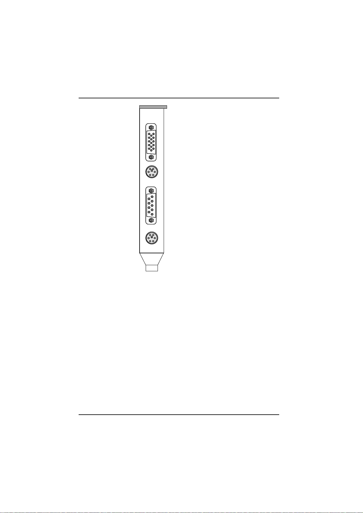
PAGE 20 HARDWARE DESCRIPTION PX1 USER MANUAL
VGA (P12)
PS/2 Mouse (P13)
RS232 Serial 1 (P15)
PS/2 Keyboard (P18)
ON-BOARD CONNECTORS
There are connectors on-board for Floppy Disk Drive, IDE, and VESA
feature connector. There are also sockets for graphics memory upgrade (if
graphics is present), SIMMs, and external battery.
Connectors are provided for the following peripheral functions:
• Second serial comms port RS232 and RS485;
• Parallel port;
• Floppy disk drives;
• Primary and secondary IDE devices.
01271019.doc Blue Chip Technology Ltd.
Page 29

PX1 USER MANUAL HARDWARE DESCRIPTION PAGE 21
In addition, connectors provide for:
• An external battery, for battery-backed SRAM installations;
• Power supply connection, for stand-alone no backplane applications ;
• Front panel components (switches, LED, speaker, etc.). This utility
connector is described in more detail below;
• On-board programming of the EPLD. This is for manufacture only,
and is not a user connection.
UTILITY CONNECTOR
The PX1 PC board provides connectors to support functions which would
normally be located within the enclosure, and also duplicate connections
for some of the external interfaces (System Speaker, System Reset
Switch, , Keyboard, Power LED Hard Drive Activity LED, an External
Battery and a Sleep/Resume switch).
SPEAKER
An on-board Piezo speaker is included. It may be disabled by removing a
link on jumper, J3. An off-board speaker may be connected to the header
(P9 pins 1 & 2) and driven independently of the on-board buzzer. The
speaker provides error beep code information during the Power-On Self
Test if the system cannot use the video interface.
RESET
Two pins of header P9 (pins 3 & 4) may be connected to a momentary
normally open SPST switch. When the switch is closed, the system will
perform a hard reset and run the POST.
IDE LED
Two pins of header P9 (pins 13 & 14) may be connected to an LED to
provide a light when an IDE hard drive connected to the on-board IDE
controller is active.
SLEEP/RESUME SWITCH
Two pins of header P9 (pins 11 & 12) may be connected to a momentaryaction, normally-open SPST switch. The switch may be used to toggle
the PC in and out of SMM modes (i.e. Sleep / Resume).
Blue Chip Technology Ltd. 01271019.doc
Page 30

PAGE 22 HARDWARE DESCRIPTION PX1 USER MANUAL
BUS CONNECTORS
The board incorporates the standard PC/AT 16-bit ISA bus, and PCI bus
connectors to passive backplanes. Additionally, the board has one set of
PC104/AT sockets for on-board expansion. See the appendices for the pinout details. Note that the PCI connector details the signals at the PX1
processor connector. These are different for each PCI slot on a backplane.
JUMPERS
Jumpers are used on the board to select various options. Some of the jumpers
are factory set to suit particular semiconductor options. These must not be
disturbed, or damage to the board may ensue. Refer to the board layout
drawing at the end of the manual for the positions of the various jumpers.
CPU FREQUENCY SELECTION J1 & J11
The external CPU bus operates at frequencies of 50, 60 and 66 MHz but is
scaled up internally giving a range of CPU frequencies of 75 to 166 MHz.
There are four links ( in two locations) involved in CPU frequency
selection: J1 and J11. Link J11 selects the host CPU operating frequency of
50, 60 and 66 MHz. Link J1 selects the clock scaling (multiplying) factor.
Link J1 is latched by the CPU on reset and used to configure the CPU phase
locked loop oscillator. This allows higher speed processors to be clocked
down (e.g. running a P133 as a P100), but over clocking processors is not
recommended as it will degrade the reliability of the device over time. Note
also that there are internal differences between each of the CPU types, i.e.
there are register differences between a P100 and a P133, it is not simply
silicon grading as was the case for 486 type CPUs.
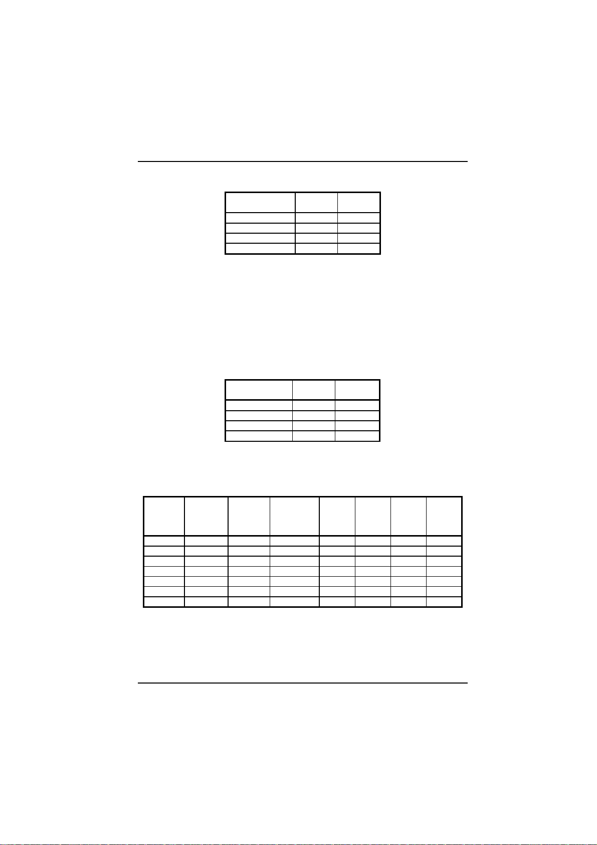
INTERNAL CPU CLOCK SPEED J1
These jumpers sets the internal CPU clock speed to either 1½, 2, 2½ or
3 times that of the external CPU clock speed. These jumpers should be
configured depending on the speed of the processor.
01271019.doc Blue Chip Technology Ltd.
Page 31
PX1 USER MANUAL HARDWARE DESCRIPTION PAGE 23
CPU CLOCK
MULTIPLIER
1.5 x Open Open
2 x Open Link
2.5 x Link Link
3 x Link Open
PAIR
A
PAIR
B
EXTERNAL CPU CLOCK SPEED J11
This jumper block sets the CPU's external operating frequency to memory
at 50, 60, or 66 MHz. The default setting depends on the specific memory
and type of Pentium processor installed. It is used in conjunction with
J1.
EXTERNAL
BUS FREQ.
50 MHz Link Link
60 MHz Link Open
66 MHz Open Link
Reserved Open Open
PAIR
A
PAIR
B
SUMMARY OF LINK SETTINGS
CPU
CORE
SPEED
(MHZ)
75 50 25 1.5 Open Open Link Link
90 60 30 1.5 Open Open Link Open
100 66 33 1.5 Open Open Open Link
120 60 30 2 Open Link Link Open
133 66 33 2 Open Link Open Link
150 60 30 2.5 Link Link Link Open
166 66 33 2.5 Link Link Open Link
Blue Chip Technology Ltd. 01271019.doc
HOST
BUS
SPEED
(MHZ)
PCI
BUS
SPEED
(MHZ)
HOST
CLK
SCALING
FACTOR
J1
A
J1
B
J11
A
J11
B
Page 32

PAGE 24 HARDWARE DESCRIPTION PX1 USER MANUAL
ON-BOARD VIDEO J6
The PX1 is equipped with a link (J6) to allow the user to disable the onboard video when external video adapters are being used. If a PCI video
adapter is fitted into a system, the on-board video will be automatically
disabled without having to fit a jumper on J6.
J6 must be fitted when using ISA based VGA adapter boards in a PX1
based system.
CMOS BATTERY SOURCE (CLEAR CMOS) J13
This jumper is used to clear the CMOS RAM in the event that the contents
become corrupt. It selects the source of backup power to the CMOS RAM,
and also allows the CMOS to be cleared down to the default settings.
Fitting the link to the “CLR” position with the power off, allows on-board
capacitors to discharge and will reset the CMOS memory. The jumper
should then be returned to the “NORM” position to restore normal
operation.
ISA BUS CLOCK J12
This jumper changes the clock frequency of the ISA bus. The effect of this
jumper on the ISA clock depends upon the setting of the CPU clock speed
jumpers. With the jumper linked, the clock frequency is divided by 8. With
the jumper open, the clock frequency is divided by 6, resulting in a higher
ISA bus frequency. The default setting for this jumper is “Linked”. In
general, this jumper should only be removed if higher ISA performance is
required, and the ISA expansion cards can handle the faster bus clock. (A
clock frequency of greater than 8.33 MHz violates the ISA specification,
although many ISA cards are designed to support higher clock frequencies.)
BUS FREQUENCY JUMPER LINKED
50 MHz 6.25 MHz 8.33 MHz
60 MHz 7.5 MHz 10 MHz
66 MHz 8.33 MHz 11 MHz
ISA BUS SPEED
( ÷ 8 )
JUMPER OPEN
( ÷ 6 )
MMX SETTINGS J10
If an MMX CPU is used the links J10 x 3 must be set to VRT. Classic
pentiums must use the standard setting.
01271019.doc Blue Chip Technology Ltd.
Page 33

PX1 USER MANUAL HARDWARE DESCRIPTION PAGE 25
TABLE OF JUMPERS
JUMPER AREA OF INFLUENCE LINK ACTION
J1 Selects the internal CPU clock
speed.
Use in conjunction with J11
J2 COM-2 RS485 Termination None
J3 On-board Speaker None
J4 Video Memory Type. FPM
J5 DRAM and Cache Voltage Select 3V
J6 On-board video select None
J7 Selects BIOS ROM Type None
J8 BIOS Memory Type
J9 CPU Core Voltage Select None
J10 CPU I/O Voltage Select
(3 links)
J11 Select External Bus Frequency.
Use in conjunction with J1
J12 Selects ISA Bus Speed.
Bus speed depends on Bus
Frequency.
J13 CMOS Battery Support None
A B
O O
O L
L L
L O
Link
Link
EDO
5V
Link
Link
None
1 - 2
2 - 3
2.9
3.3
3.45
3.6
VRT
STD
A B
L L
L O
O L
O O
None
Link
CLR
NORM
(External CPU speed)
x 1.5
x 2
x 2.5
x 3
Unterminated
Terminated by 100R + µ1
Disabled
Enabled
Fast Page Memory
Extended Data Out Memory
3 Volt
5 Volt (Default)
Enabled
Disabled
EPROM (Default)
Flash PROM
Factory setting only.
5 V Flash or EPROM (Default)
12 V Flash
Reserved
Not Allowed
2V9 CPU core
3V3 CPU core
3V45 CPU core
3V6 CPU core
VRT CPU (J10)
Standard CPU
External Bus Frequency
50 MHz
60 MHz
66 MHz
Reserved
(Bus speed) / 6
(Bus speed) / 8
Not Allowed
Clear CMOS RAM
Use on-board battery
In the table “L” indicates the presence of a link, “O” the absence.
Blue Chip Technology Ltd. 01271019.doc
Page 34

PAGE 26 HARDWARE DESCRIPTION PX1 USER MANUAL
STATUS LEDS
Along the top edge of the PCB on the reverse side is a row of LEDs. These
are arranged in groups to indicate the status of various board functions:
P.O.S.T. DISPLAY
Red LEDs D10 to D17 inclusive display the Power On Self Test (POST)
data byte. Diode D17 represent the LSB and D10 the MSB. The LED is
illuminated when the POST data bit is 1. See the Appendix for details of
the error codes.
POWER SUPPLY INDICATORS
Green LEDs D5-D9 inclusive show the presence of the power supplies.
Each LED is illuminated when the appropriate voltage is present.
D9 Host CPU IO and chipset supply (3.3 Volts)
D8 + 5 Volt (Vcc) supply
D7 + 12 Volt supply
D6 - 12 Volt supply
D5 - 5 Volt supply
IDE ACTIVITY DISPLAY
Yellow LED D4 indicates primary and secondary IDE activity (Hard disk
or CD-ROM) and is illuminated when active.
SYSTEM RESET STATUS
Red LED D3 indicates the system reset status. The LED is illuminated
when in held in reset.
MONITOR MICROCONTROLLER STATUS
Yellow LED D2 indicates the status of the monitor microcontroller (if
fitted). The LED is illuminated when a fault condition has occurred.
WATCHDOG TIMER STATUS
Yellow LED D1 indicates the watchdog time out status. The LED is
illuminated when a timeout has occurred.
01271019.doc Blue Chip Technology Ltd.
Page 35

PX1 USER MANUAL HARDWARE DESCRIPTION PAGE 27
USER-INSTALLABLE UPGRADES
SYSTEM MEMORY
The table shows the possible memory combinations. The PX1 will support
both Fast Page DRAM or EDO DRAM SIMMs, but they cannot be mixed
within the same memory bank. If Fast Page DRAM and EDO DRAM
SIMMs are installed in separate banks, each bank will be optimised for
maximum performance. Parity generation and detection are NOT
supported, but parity SIMMs (x36) may be used.
SIMM requirements are 70ns Fast Page Mode or 60nS EDO DRAM (70 ns
EDO may be used with a 60 MHz or slower external CPU clock) with tinlead connectors.
SIMM 1,2 (BANK A)
SIMM TYPE (AMOUNT)
1M X 32 (4 MB) Empty 8 MB
1M X 32 (4 MB) 1M X 32 (4 MB) 16 MB
1M X 32 (4 MB) 2M X 32 (8 MB) 24 MB
1M X 32 (4 MB) 4M X 32 (16 MB) 40 MB
1M X 32 (4 MB) 8M X 32 (32 MB) 72 MB
2M X 32 (8 MB) Empty 16 MB
2M X 32 (8 MB) 1M X 32 (4 MB) 24 MB
2M X 32 (8 MB) 2M X 32 (8 MB) 32 MB
2M X 32 (8 MB) 4M X 32 (16 MB) 48 MB
2M X 32 (8 MB) 8M X 32 (32 MB) 80 MB
4M X 32 (16 MB) Empty 32 MB
4M X 32 (16 MB) 1M X 32 (4 MB) 40 MB
4M X 32 (16 MB) 2M X 32 (8 MB) 48 MB
4M X 32 (16 MB) 4M X 32 (16 MB) 64 MB
4M X 32 (16 MB) 8M X 32 (32 MB) 96 MB
8M X 32 (32 MB) Empty 64 MB
8M X 32 (32 MB) 1M X 32 (4 MB) 72 MB
8M X 32 (32 MB) 2M X 32 (8 MB) 80 MB
8M X 32 (32 MB) 4M X 32 (16 MB) 96 MB
8M X 32 (32 MB) 8M X 32 (32 MB) 128 MB
SIMM 3,4 (BANK B)
SIMM TYPE (AMOUNT)
TOTAL SYSTEM
Note: SIMMs may be parity (x 36) or non-parity (x 32)
MEMORY
Blue Chip Technology Ltd. 01271019.doc
Page 36

PAGE 28 HARDWARE DESCRIPTION PX1 USER MANUAL
EDO DRAM
Extended Data Out (or Hyper Page) DRAM is designed to improve the
DRAM read performance. EDO DRAM holds the memory data valid
until the next CAS# falling edge, unlike standard fast page mode DRAM
which tri-states the memory data when CAS# negates to precharge for
the next cycle. With EDO, the CAS# precharge overlaps the data valid
time, allowing CAS# to negate earlier while still satisfying the memory
data valid window time.
REAL TIME CLOCK BATTERY REPLACEMENT
The on-board battery may be replaced using a Crompton Eternacell type
T048AA9 lithium battery, or equivalent. This battery has a 1000 mAh
rating.
CPU UPGRADE
A Type 7 Zero Insertion Force (ZIF) socket provides users with a
performance upgrade path to the Pentium Overdrive Processors.
GRAPHICS MEMORY UPGRADE
The PX1 single board PC has 1 MB of Fast Page DRAM installed for
graphics. Two SOJ type sockets (IC4 & IC5 on the underside of the board)
provide for upgrade of the graphics DRAM. Two 256K x 16, 60 ns DRAMs
may be installed to provide a total of 2 MB of graphics DRAM. Note these
must be installed in pairs.
The DRAM must be of the “Dual CAS” type and not the “Dual Write” type.
Suitable types are:
Toshiba: TC514260BJ-60
NEC: µPD424260LE-60
Hitachi: HM514260CJ-6
01271019.doc Blue Chip Technology Ltd.
Page 37

PX1 USER MANUAL SOFTWARE DESCRIPTION PAGE 29
SOFTWARE DESCRIPTION
BIOS SETUP
This section details the BIOS CMOS Setup Utility. The parameters described
below are based on BIOS version 1.10; other BIOS versions may differ from
the description below as new features are added.
OVERVIEW OF THE SETUP MENU SCREENS
The Setup program initially displays the Main menu screen. In each screen
there are options for modifying the system configuration. Select a sub-menu
screen by pressing the up <↑> or down <↓> arrow keys, followed by <Enter>.
Within the menu use the up <↑> or down <↓> keys to select an item, then use
<PgUp> or <PgDn> to modify it. For certain items, pressing <Enter> will
bring up a subscreen. After you have selected an item, use the <PgUp> or
<PgDn> keys to modify the setting.
MAIN SCREEN
Shows the following menu:
Standard Setup
Advanced CMOS Setup
Advanced Chipset Setup
Power Management Setup
PCI / PnP Setup
Peripheral Setup
Auto Detect Hard Disk
Change User Password
Change Supervisor Password
Auto Configuration with Optimal Settings
Auto Configuration with Fail Safe Settings
Save Settings and Exit
Exit without Saving
Blue Chip Technology Ltd. 01271019.doc
Page 38

PAGE 30 SOFTWARE DESCRIPTION PX1 USER MANUAL
Their operation is as follows:
STANDARD SETUP
For setting up and modifying basic items such as floppy disk drives, hard
drives, and system time & date.
ADVANCED CMOS SETUP
For modifying the more advanced features of the PC (e.g. system bootup
options).
ADVANCED CHIPSET SETUP
For modifying hardware level options.
POWER MANAGEMENT SETUP
For specifying the “Green PC” features such as IDE and VGA timeouts.
PCI / PNP SETUP
For specifying Plug and Play options (e.g. IRQ assignments).
PERIPHERAL SETUP
For specifying the system peripheral options such as serial and parallel
port modes.
AUTO DETECT HARD DISK
Automatically determines the parameters of any IDE devices connected,
and sets up the parameters for “USER DEFINED” drives.
CHANGE USER PASSWORD
Allows the password for the user level options to be set or changed. This
option cannot be changed unless a supervisor password has been set.
CHANGE SUPERVISOR PASSWORD
Allows the password for the supervisor level options to be changed.
01271019.doc Blue Chip Technology Ltd.
Page 39

PX1 USER MANUAL SOFTWARE DESCRIPTION PAGE 31
AUTO CONFIGURATION WITH OPTIMAL SETTINGS
Resets the CMOS setup options to a high performance configuration. The
optimal default settings are best case values and should optimise the
system performance. If CMOS RAM is corrupted, the optimal settings
are loaded automatically.
AUTO CONFIGURATION WITH FAIL SAFE SETTINGS
Resets the CMOS setup options to a lower performance but guaranteed
working configuration. The fail safe settings provide far from optimal
system performance, but are the most stable settings. Use these settings
as an diagnostics aid if the system is performing erratically.
SAVE SETTINGS AND EXIT
When selected, this allows you to save the change to CMOS and exit the
Setup program. You can also press the <F10> key anywhere in the Setup
program to do this.
EXIT WITHOUT SAVING
When selected, this allows you to exit the Setup program without saving
any changes. This means that any changes made while in the Setup
program will be discarded and NOT SAVED. Pressing the <Esc> key in
any of the four main screens will do this.
Blue Chip Technology Ltd. 01271019.doc
Page 40

PAGE 32 SOFTWARE DESCRIPTION PX1 USER MANUAL
OVERVIEW OF THE SETUP KEYS
SETUP KEY DESCRIPTION
<F1> Pressing the <F1> key brings up a help screen for the currently
<Esc> Pressing the <Esc> key takes you back to the previous screen.
<PgUp>
<PgDn>
<↑> Pressing the up <↑> key changes the selection to the previous item or
<↓> Pressing the down <↓> key changes the selection the to the next item
<←> <→> Pressing the left <←> or right <→> keys in the Main, Advanced,
<F5> Pressing the <F5> key allows you to Load Setup Defaults (see later in
<F6> Pressing the <F6> key allows you to Discard Changes (see later in this
<F10> Pressing the <F10> key allows you to Exit Saving Changes (see later
selected item.
Pressing it in the Main, Advanced, Security, or Exit screen allows you
to Exit Discarding Changes (see later in this chapter).
Pressing either key moves the selection of the current item up or down
the available options.
option.
or option.
Security, or Exit menu screens changes the menu screen. Pressing
either key in a subscreen does nothing.
this chapter).
chapter).
in this chapter).
STANDARD SETUP
This section describes the Setup options found on the standard setup screen.
SYSTEM DATE
When selected, this allows you to set the current date by specifying a
date, month and year.
SYSTEM TIME
When selected, this allows you to set the current time by entering values
for hours, minutes and seconds..
FLOPPY A: TYPE
When selected, this allows you to cycle through the available options to
specify the physical size and capacity of the diskette drive. The options
are Disabled; 360 KB, 5.25-inch; 1.2 MB, 5.25-inch; 720 KB, 3.5-inch;
1.44/1.25 MB, 3.5-inch; 2.88 MB, 3.5-inch. The default is 1.44 MB, 3.5inch.
01271019.doc Blue Chip Technology Ltd.
Page 41

PX1 USER MANUAL SOFTWARE DESCRIPTION PAGE 33
FLOPPY B: TYPE
When selected, this allows you to cycle through the available options to
specify the physical size and capacity of the diskette drive. The options
are Disabled, 360 KB, 5.25-inch; 1.2 MB, 5.25-inch; 720 KB, 3.5-inch;
1.44/1.25 MB, 3.5-inch; 2.88 MB, 3.5-inch. The default is Disabled.
PRIMARY IDE MASTER
This reports if a primary master IDE hard disk is connected to the system
and allows for the configuration of drive parameters.
When selected, this allows the manual configuration of the hard drive or
have the system auto configure it. The options are Auto Configured, User
Definable and Disabled. There are also options for IDE CD-ROM and
46 predefined hard drive types. If you select User Definable then the
Number of Cylinders, Number of Heads, and Number of Sectors can each
be modified. The default for this is “Auto”.
PRIMARY IDE SLAVE
This reports if a primary slave IDE hard disk is connected to the system.
It is configured exactly as described under Primary IDE Master above.
The default is “Not Installed”.
SECONDARY IDE MASTER
This reports if a secondary master IDE hard disk is connected to the
system. It is configured exactly as described under Primary IDE Master
above. The default is “Not Installed”.
SECONDARY IDE SLAVE
This reports if a secondary slave IDE hard disk is connected to the
system. It is configured exactly as described under Primary IDE Master
above. The default is “Not Installed”.
NUMBER OF CYLINDERS
If Hard Disk Type is set to User Definable, you must type the correct
number of cylinders for your hard disk. If Hard Disk Type is set to Auto
Configured, this reports the number of cylinders for your hard disk and
cannot be modified.
Blue Chip Technology Ltd. 01271019.doc
Page 42

PAGE 34 SOFTWARE DESCRIPTION PX1 USER MANUAL
NUMBER OF HEADS
If Hard Disk Type is set to User Definable, you must type the correct
number of heads for your hard disk. If Hard Disk Type is set to Auto
Configured, this reports the number of heads for your hard disk and
cannot be modified.
NUMBER OF SECTORS
If Hard Disk Type is set to User Definable, you must type the correct
number of sectors for your hard disk. If Hard Disk Type is set to Auto
Configured, this reports the number of sectors for your hard disk and
cannot be modified.
BOOT SECTOR VIRUS DETECTION
If set to “Enabled” this will flag a warning when the boot sector of a hard
disk drive is changed. The options are “Enabled” and “Disabled”. The
default is “Disabled”.
ADVANCED CMOS SETUP
QUICK BOOT
Set this option to “Enabled “ to instruct the BIOS to boot quickly.
If set to “Enabled” the BIOS does not test memory above 1 MB and the
BIOS does not wait up to 40 seconds for a READY signal from the hard
drive. If the READY signal is not received immediately from the IDE
drive, it is not configured (as if it was absent). The default is “Disabled”.
BOOTUP SEQUENCE
This option specifies the sequence of the boot drives (floppy drive A:,
hard drive C:, or a CD-ROM drive). The settings are:
C: A: CD-ROM
A: C: CD-ROM
CD-ROM C: A:
The default is A: C: CD-ROM.
01271019.doc Blue Chip Technology Ltd.
Page 43

PX1 USER MANUAL SOFTWARE DESCRIPTION PAGE 35
BOOT CPU SPEED
Allows the system’s boot speed to be set. The options are “Low” and
“High”. The optimal setting is “High”, the fail-safe is “Low”. If High is
selected, boot-up occurs at full speed. If Low is selected, the board
operates at a slower speed (approximately equivalent to 25 MHz PC-AT).
Default is low.
BOOT UP NUM LOCK
Allows you to set the start up state of “Num Lock” on your keyboard. The
options are “On” and “Off”. The default is On.
FLOPPY DRIVE SEEK
Set this option to specify floppy drive A: will perform a seek operation on
system boot. are “Enabled” and “Disabled”. The default setting is
enabled.
MOUSE SUPPORT
When this option is enabled the BIOS will support a PS/2 style mouse.
The options are “Enabled” and “Disabled”. The default setting is
enabled.
SYSTEM KEYBOARD
This option specifies that a keyboard is attached to the computer. The
settings are Present or Absent. The Optimal and Fail-Safe default
settings are Present.
PRIMARY DISPLAY
This option specifies the type of display monitor and adapter in the
computer. The settings are Mono, CGA40, CGA80, EGA/VGA, or
Absent. The Optimal and Fail-Safe default settings are VGA/EGA.
PASSWORD CHECK
This option enables password checking every time the computer is
powered on or every time Setup is executed. If Always is chosen, a user
password prompt appears every time the computer is turned on. If Setup
is chosen, the password prompt appears if Setup is executed.
Blue Chip Technology Ltd. 01271019.doc
Page 44

PAGE 36 SOFTWARE DESCRIPTION PX1 USER MANUAL
OS/2 COMPATIBLE MODE
Set this option to Enabled to permit AMIBIOS to run with IBM OS/2.
The settings are Enabled or Disabled. The default settings are Disabled.
WAIT FOR F1 IF ERROR
AMIBIOS POST error messages are followed by:
Press <F1> to continue
If this option is set to Disabled, AMIBIOS does not wait for you to press
the <F1> key after an error message. The settings are Disabled or
Enabled. The Optimal and Fail-Safe default settings are Enabled.
HIT DEL MESSAGE DISPLAY
Set this option to Disabled to prevent
Hit <DEL> if you want to run Setup
from appearing on the first AMIBIOS screen when the computer boots.
The settings are Disabled or Enabled. The Optimal and Fail-Safe default
settings are Enabled.
INTERNAL CACHE
This option specifies the caching algorithm used for L1 internal cache
memory. The settings are :
SETTING DESCRIPTION
Disabled Neither L1 internal cache memory on the CPU or L2 secondary
WriteBack
(default)
WriteThru Use the write through caching algorithm
01271019.doc Blue Chip Technology Ltd.
cache memory is disabled
Use the write-back caching algorithm
Page 45

PX1 USER MANUAL SOFTWARE DESCRIPTION PAGE 37
EXTERNAL CACHE
This option specifies the caching algorithm used for L2 secondary
(external) cache memory. The settings are :
SETTING DESCRIPTION
Disabled L2 cache is disabled
WriteBack L2 cache is write back. (Deafult)
WriteThru L2 cache is write through
SYSTEM BIOS SHADOW CACHEABLE
When this option is set to Enabled, the contents of the F0000h system
memory segment can be read from or written to L2 secondary cache
memory. The contents of the F0000h memory segment are always copied
from the BIOS ROM to system RAM for faster execution.
The settings are Enabled or Disabled. The Optimal default setting is
Enabled. The Fail-Safe default is Disabled. Default is Enabled.
C000, 16K Shadow
C400, 16K Shadow
C800, 16K Shadow
CC00, 16K Shadow
D000, 16K Shadow
D400, 16K Shadow
D800, 16K Shadow
DC00, 16K Shadow
These options control the location of the contents of the 16KB blocks of
ROM beginning at the specified memory location. If no adapter ROM is
using the named ROM area, this area is made available to the local bus.
Blue Chip Technology Ltd. 01271019.doc
Page 46

PAGE 38 SOFTWARE DESCRIPTION PX1 USER MANUAL
The settings are :
SETTING DESCRIPTION
Enabled The contents of C0000h - C3FFFh are written to the same
Cache The contents of the named ROM area are written to the same
Disabled The video ROM is not copied to RAM. The contents of the video
address in system memory (RAM) for faster execution.
address in system memory (RAM) for faster execution, if an
adapter ROM will be using the named ROM area. Also, the
contents of the RAM area can be read from and written to cache
memory.
ROM cannot be read from or written to cache memory.
The default setting is Cache for C000 and C400; disabled for the
remainder.
In the AMIBIOS for the Intel Triton chipset, the E000h page is used as
ROM during POST, but shadowing is disabled and the ROM CS# signal
is disabled to make the E000h page available on the local bus.
ADVANCED CHIPSET SETUP
MEMORY HOLE
Use this option to specify an area in memory that cannot be addressed on
the ISA bus. The settings are Disabled, 512-640K or 15-16MB. The
default setting is Disabled.
INSTALLED MEMORY
Use this option to specify the total amount of memory installed in the
system when using the memory hole. This option should ONLY be used
with OS/2. The options are Disabled, 32MB, and 64MB. The optimal
and fail safe defaults are Disabled.
DRAM SPEED
Specify the RAS access speed of the SIMMs installed in the motherboard
as system memory. The settings are 60nS or 70nS. The default is 70nS.
01271019.doc Blue Chip Technology Ltd.
Page 47

PX1 USER MANUAL SOFTWARE DESCRIPTION PAGE 39
Caution
If you have installed SIMMs with different speeds in the motherboard,
select the speed of the slowest SIMM. You must always use SIMMs
that have the same speed within each memory bank.
IRQ12/M MOUSE FUNCTION
Set this option to Enabled to specify that IRQ12 will be used for the
mouse. The settings are Disabled or Enabled. The Optimal and FailSafe default settings are Enabled.
8-BIT I/O RECOVERY TIME (SYSCLK)
This option specifies the length of the delay (in units of SYSCLKs)
inserted between consecutive 8-bit I/O operations. The settings are
1,2,3,4,5,6,7, or 8. the Optimal and Fail-Safe default settings are 8.
16-BIT I/O RECOVERY TIME (SYSCLK)
This option specifies the length of the delay (in SYSCLKs) inserted
between consecutive 16-bit I/O operations. The settings are 1,2,3,4,5,6,7
or 8. The Optimal and Fail-Safe default settings are 4.
POWER MANAGEMENT SETUP
POWER MANAGEMENT / APM
Set this option to Enabled to enable the power management and APM
(advanced Power Management) features.
The settings are Enabled, Disabled or Inst-On. The default settings are
Disabled.
INSTANT ON SUPPORT
If this option is set in Power Management / APM it allows the computer
to go to full power on mode when leaving a power-conserving state.
AMIBIOS uses the RTC Alarm function to wake the computer at a prespecified time. The settings are 1 to 14 minutes, or Disabled. The
default settings are Disabled.
Blue Chip Technology Ltd. 01271019.doc
Page 48

PAGE 40 SOFTWARE DESCRIPTION PX1 USER MANUAL
GREEN PC MONITOR POWER STATE
This option specifies the power management state that the Green PCcompliant video monitor enters after the specified period of display
inactivity has expired. The settings are, Off, Standby, or Suspend. The
default settings are Standby.
VIDEO POWER DOWN MODE
This option specifies the power management state that the video
subsystem enters after the specified period of display inactivity has
expired. The settings are Disabled, Standby or Suspend. The default
settings are Disabled.
HARD DISK POWER DOWN MODE
This option specifies the power management state that the hard disk
drive enters after the specified period of display inactivity has expired.
The settings are Disabled, Standby, or Suspend. The default settings are
Disabled.
HARD DISK TIMEOUT (MIN)
This option specifies the length of a period of hard disk inactivity. When
this period expires, the hard disk drive enters the power-conserving mode
specified in the Hard Disk Power Down Mode option described above.
The settings are Disabled, 1 Min (minutes), and all one minute intervals
up to and including 15 Min. The default settings are Disabled.
STANDBY TIMEOUT
This option specifies the length of the period of system inactivity when
the computer is in Full-On mode before the computer is placed in
Standby mode. In Standby mode, some power use is curtailed. The
settings are Disabled, 1 Min, 2 Min and all one minute intervals up to
and including 15 Min. The default settings are Disabled.
SUSPEND TIMEOUT
This option specifies the length of the period of system inactivity when
the computer is already in Standby mode before the computer is placed in
Suspend mode. In Suspend mode, nearly all power use is curtailed. The
settings are Disabled, 1 Min, 2 Min, and all one minute intervals up to
and including 15 Min. The default settings are Disabled.
01271019.doc Blue Chip Technology Ltd.
Page 49

PX1 USER MANUAL SOFTWARE DESCRIPTION PAGE 41
SLOW CLOCK RATIO
This option specifies the speed at which the system clock runs in power
saving modes. The settings are expressed as a ratio between the normal
clock speed and the power down clock speed. The settings are 1:1, 1:2
(half as fast as normal), 1:4 ((the normal clock speed), 1:8, 1:16, 1:32,
1:64, or 1:128. The default setting is 1:8.
DISPLAY ACTIVITY
This option specifies if AMIBIOS is to monitor activity on the display
monitor for power conservation purposes. When this option is set to
Monitor and there is no display activity for the length of time specified in
the value in the Full-On to Standby Timeout (Min) option, the computer
enters a power saving state. The settings are Monitor or Ignore. The
default settings are Ignore.
IRQ 3, 4, 5, 7, 9, 10, 11, 12, 13, 14, 15
These options enable event monitoring. When the computer is in a
power saving mode, activity on the named interrupt request line is
monitored by AMIBIOS. When any activity occurs, the computer enters
Full On mode.
Each of these options can be set to Monitor or Ignore. The settings are:
OPTIMAL FAIL-SAFE
IRQ 3 Monitor Ignore
IRQ 4 Monitor Ignore
IRQ 5 Ignore Ignore
IRQ 7 Monitor Ignore
IRQ 9 Ignore Ignore
IRQ 10 Ignore Ignore
IRQ 11 Ignore Ignore
IRQ 12 Monitor Ignore
IRQ 13 Ignore Ignore
IRQ 14 Monitor Ignore
IRQ 15 Monitor Ignore
Blue Chip Technology Ltd. 01271019.doc
Page 50

PAGE 42 SOFTWARE DESCRIPTION PX1 USER MANUAL
PCI / PNP SETUP
PLUG AND PLAY AWARE OS
Set this option to Yes if the operating system installed in the computer is
Plug and Play-aware. AMIBIOS only detects and enables PnP ISA
adapter cards that are required for system boot. The Windows 95
operating system detects and enables all other PnP-aware adapter cards.
Windows 95 is PnP-aware. Set this option to No if the operating system
(such as DOS, OS/2, Windows 3.x) does not use PnP. You must set this
option correctly or PnP-aware adapter cards installed in your computer
will not be configured properly. The settings are No or Yes. The
Optimal and Fail-Safe default settings are No.
PCI BURST MODE
Set this option to Enabled to enable PCI burst mode. The settings are
Disabled or Enabled. The Optimal default setting is Enabled. The FailSafe default setting is Disabled.
PCI CONCURRENCY
Set this option to “Enable” to allow PCI peer to peer cache concurrency.
Options are Enabled or Disabled. The default is Enabled.
PCI LATENCY TIMER (IN PCI CLOCKS)
This option sets latency of all PCI devices on the PCI bus. The settings
are in units equal to PCI clocks. The settings are 32, 64, 96, 128, 160,
192, 224, or 248. The Optimal and Fail-Safe default settings are 64.
ALLOCATE IRQ TO PCI VGA
Use this option to specify whether the PCI device initialisation code
within the BIOS should allocate an IRQ to the PCI VGA controller.
Setting this option to YES reduces the available IRQ lines to the rest of
the system by 1. The options are Yes or No. The optimal and fail safe
defaults are No.
01271019.doc Blue Chip Technology Ltd.
Page 51

PX1 USER MANUAL SOFTWARE DESCRIPTION PAGE 43
PCI VGA PALETTE SNOOP
This option must be set to Enabled if any ISA adapter card installed in
the computer requires VGA palette snooping. The settings are Disabled
or Enabled. The Optimal and Fail-Safe default settings are Disabled.
PCI IDE BUS/MASTER
Set this option to Enabled to specify that the IDE controller on the PCI
local bus has bus mastering capability. The settings are Disabled or
Enabled. The Optimal and Fail-Safe default settings are Disabled.
OFFBOARD PCI IDE CARD
This option specifies if an offboard PCI IDE controller adapter card is
used in the computer. You must also specify the PCI expansion slot on
the motherboard where the offboard PCI IDE controller card is installed.
If an offboard PCI IDE controller is used, the on-board IDE controller on
the motherboard is automatically disabled. The settings are Disabled,
Auto, Slot1, Slot2, Slot3, or Slot 4.
If Auto is selected, AMIBIOS automatically determines the correct
setting for this option. The Optimal and Fail-Safe default settings are
Auto.
In the AMIBIOS for the Intel Triton chipset, this option forces IRQ 14
and 15 to a PCI slot on the PCI local bus. This is necessary to support
non-compliant PCI IDE adapter cards.
OFFBOARD PCI IDE PRIMARY IRQ
This option specifies the PCI interrupt used by the primary IDE channel
on the offboard PCI IDE controller. The settings are Disabled, INTA,
INTB, INTC, INTD or Hardwired. The Optimal and Fail-Safe default
settings are Disabled.
OFFBOARD PCI IDE SECONDARY IRQ
This option specifies the PCI interrupt used by the secondary IDE
channel on the offboard PCI IDE controller. The settings are Disabled,
INTA, INTB, INTC, INTD or Hardwired. The Optimal and Fail-Safe
default settings are Disabled.
Blue Chip Technology Ltd. 01271019.doc
Page 52

PAGE 44 SOFTWARE DESCRIPTION PX1 USER MANUAL
DMA CHANNELS 0, 1, 3, 5, 6, 7
These options specify the bus to which the DMA channel is allocated.
These options determine if AMIBIOS should remove a DMA channel
from the available pool passed to BIOS configurable devices. The
available pool is determined by reading the ESCD NVRAM. If more
DMA channels must be removed from the pool, the end user can use
these PCI/PnP Setup options to remove the channel by assigning the
option to the ISA/EISA setting. Onboard I/O is configurable by
AMIBIOS. The DMA channels used by onboard I/O are configured as
PCI/PnP.
The default settings are:
OPTIMAL FAILSAFE
Channel 0 PnP PnP
Channel 1 PnP PnP
Channel 3 ISA/EISA ISA/EISA
Channel 5 PnP PnP
Channel 6 PnP PnP
Channel 7 PnP PnP
IRQ 3, 4, 5, 7, 9, 10, 11, 14, 15
These options specify the bus that the named interrupt request lines
(IRQs) are used on. These options allow you to specify IRQs for use by
legacy ISA adapter cards.
These options determine if AMIBIOS should remove an IRQ from the
pool of available IRQs passed to BIOS configurable devices. The
available IRQ pool is determined by reading the ESCD NVRAM. If
more IRQs must be removed from the pool, the end user can use these
PCI/PnP Setup options to remove the IRQ by assigning the option to the
ISA/EISA setting. Onboard I/O is configurable by AMIBIOS. The IRQs
used by onboard I/O are configured as PCI/PnP.
01271019.doc Blue Chip Technology Ltd.
Page 53

PX1 USER MANUAL SOFTWARE DESCRIPTION PAGE 45
The optimal and fail-safe settings are:
OPTIMAL FAILSAFE
IRQ 3 ISA/EISA ISA/EISA
IRQ 4 ISA/EISA ISA/EISA
IRQ 5 PnP PnP
IRQ 7 ISA/EISA ISA/EISA
IRQ 9 PnP PnP
IRQ 10 PnP PnP
IRQ 11 PnP PnP
IRQ 14 PnP PnP
IRQ 15 PnP PnP
RESERVED MEMORY SIZE
This option specifies the size of the memory area reserved for legacy ISA
adapter cards.
The settings are Disabled, 16K, 32K, or 64K. The Optimal and Fail-Safe
default settings are Disabled.
RESERVED MEMORY ADDRESS
This option specifies the beginning address (in hex) of the reserved
memory area. The specified ROM memory area is reserved for use by
legacy ISA adapter cards.
The settings are C0000, C4000, C8000, CC000, D0000, D4000, D8000,
DC000. The Optimal and Fail-Safe default settings are C8000.
PERIPHERAL SETUP
Peripheral Setup options are displayed by choosing the Peripheral Setup
icon from the WINBIOS Setup main menu. All Peripheral Setup options
are described in this section.
ONBOARD PCI IDE
This option specifies the onboard IDE controller channels that will be
used. The settings are Primary, Secondary, Both or Disabled. The
Optimal and Fail-Safe default settings are Both.
Blue Chip Technology Ltd. 01271019.doc
Page 54

PAGE 46 SOFTWARE DESCRIPTION PX1 USER MANUAL
ONBOARD FDC
This option enables the floppy drive controller on the PC board. The
settings are Auto, Enabled or Disabled. The default setting is Auto.
ONBOARD SERIAL PORT1
This option enables serial port 1 on the board and specifies the based I/O
port address for serial port 1.
The settings are Auto, 3F8h, 3E8h, 2F8h, 2E8h, or Disabled. The
default setting is Auto.
ONBOARD SERIAL PORT2
This option enables serial port 2 on the board and specifies the base I/O
port address for serial port 2.
The settings are Auto, 3F8h, 3E8h, 2F8h, 2E8h, or Disabled. The
default setting is Auto.
ONBOARD PARALLEL PORT
This option enables the parallel port on the board and specifies the
parallel port based I/O port address. The settings are Auto, 378h, 278h,
3BCh, or Disabled. The default setting is Auto.
PARALLEL PORT MODE
This option specifies the parallel port mode. ECP and EPP are both bidirectional data transfer schemes that adhere to the IEEE P1284
specifications. The settings are :
SETTING DESCRIPTION
Normal The normal parallel port mode is used. This is the default
Bi-Dir Use this setting to support bi-directional transfers on the parallel
EPP The parallel port can be used with devices that adhere to the
ECP The parallel port can be used with devices that adhere to the
01271019.doc Blue Chip Technology Ltd.
setting.
port.
Enhanced Parallel Port (EPP) specification. EPP uses the
existing parallel port signals to provide asymmetric bi-directional
data transfer driven by the host device.
Extended Capabilities Port (ECP) specification. ECP uses the
DMA protocol to achieve transfer rates of approximately 2.5Mbs.
ECP provides symmetric bi-directional communications.
Page 55

PX1 USER MANUAL SOFTWARE DESCRIPTION PAGE 47
PARALLEL PORT IRQ
Selects which IRQ is assigned to the parallel port. Available options are
Auto, 5, or 7. The default is Auto.
PARALLEL PORT DMA
This option is only available if the setting for the Parallel Port Mode
option is ECP.
The settings are Auto, None, DMA CH 0, DMA CH 1, DMA CH 2, or
DMA CH 3. (CH = channel). The default setting is Disabled.
HARDWARE IO PORT BASE ADDRESS
This specifies the base address of the PX1 configuration and control
registers. The permissible options are:
100 hex, 300 hex, 400 hex, 500 hex, 600 hex, 700 hex, 800 hex, 900 hex,
A00 hex, B00 hex, C00 hex, D00 hex, E00 hex, and F00 hex. Note the
absence of 200 hex in the list. The default is 100 hex.
SERIAL PORT 2 MODE
Specifies whether the second serial port will be used as RS232 or RS485.
Options are RS232 and RS485. The optimal and fail safe defaults are
RS232.
RS485 DUPLEX MODE
Specifies whether the second serial port will be used as full or half duplex
when running in RS485 mode. This option is only available when the
options ‘Serial Port 2 Mode’ is set to RS485. The options are FULL or
HALF. The Optimal and Fail Safe defaults are FULL.
FEATURE CONNECTOR
Specifies whether the S3 feature connector is enabled or disabled. The
options are Enabled and Disabled. The Optimal and Fail Safe defaults
are Disabled.
If set to enabled and a device is not connected to the feature connector the
display will blank when the feature connector is initialised.
When the feature connector is enabled the S3 VGA Controller will only
use 1MB of video memory limiting the resolutions available.
Blue Chip Technology Ltd. 01271019.doc
Page 56

PAGE 48 SOFTWARE DESCRIPTION PX1 USER MANUAL
BIOS EXTENSIONS
Specifies whether the PX1 BIOS extensions are available. See the
section “BIOS Extensions Software Interface” for details of the functions
available. The options are Enabled and Disabled. The optimal and fail
safe defaults are Disabled.
01271019.doc Blue Chip Technology Ltd.
Page 57

PX1 USER MANUAL SOFTWARE DESCRIPTION PAGE 49
DISKONCHIP 2000 SUPPORT
The PX-1 supports the use of M-Systems DiskOnChip 2000 Flash Module,
the notes below detail the use of the device, please consult the user manual
if any more detail is required.
1. PREFACE
This note describes how to integrate the DiskOnChip 2000 with PC
compatible systems. The DiskOnChip 2000 is a single chip FlashDisk
designed to plug into a standard 32-pin EEPROM socket. The DiskOnChip
2000 should be mapped into an 8KByte window in the BIOS expansion
address space of the PC, which is usually located between address 0C0000H
to 0EFFFFH.
The DiskOnChip 2000 contains a built-in copy of the M-Systems industrystandard TrueFFS software, which makes the DiskOnChip operate as a
standard disk drive. The DiskOnChip 2000 can contain the operating
system in it to allow systems to boot without a hard disk. The DiskOnChip
2000 can also be configured as the boot device in systems with a hard disk
(see below “Configuring the DiskOnChip 2000 as the first drive”).
The DiskOnChip is a self-contained device. The installation of the
DiskOnChip does not require any software installation. The design of the
DiskOnChip allows for full upward and downward compatibility. While
available today in capacities of 2 to 72MBytes, future DiskOnChip devices
with higher densities, will be fully compatible with standard DiskOnChip
sockets. The basic design of the DiskOnChip actually supports an unlimited
capacity.
Blue Chip Technology Ltd. 01271019.doc
Page 58

PAGE 50 SOFTWARE DESCRIPTION PX1 USER MANUAL
2. OPERATING THE DISKONCHIP
2.1 INSTALLING THE DISKONCHIP 2000
When installing or removing the DiskOnChip, be sure to first touch a
grounded surface to discharge any static electricity from your body. Use the
following procedure to install the DiskOnChip:
Align pin 1 on the DiskOnChip with pin 1 of Flash socket.
Push the DiskOnChip into the socket carefully until it is fully seated.
Check to make sure the DiskOnChip is installed securely, and there are no
bent pins.
Caution: The DiskOnChip may be permanently damaged if installed
incorrectly!
To install the DiskOnChip as drive C on a system without a hard disk, set
the CMOS setup of drive C to “not installed” (indicating that no physical
magnetic disk is installed), and reboot the computer. The DiskOnChip 2000
will install as drive C. The DiskOnChip needs to be formatted with the
System files in order for it to be a bootable drive. See “Configuring the
DiskOnChip as the BOOT device” below.
To install the DiskOnChip as drive D on a system with a hard disk, just
reboot the system, and the DiskOnChip will install as drive D.
To install the DiskOnChip as Drive C on a system with a hard disk, see
below “Configuring the DiskOnChip as the first drive”.
2.2 CONFIGURING THE DISKONCHIP 2000 AS THE BOOT
DEVICE
In order to configure the DiskOnChip as the boot device, the operating
system files need to be copied into it. Copying the operating system files
into DiskOnChip Should be done like in any other hard disk. The following
is an example of a typical initialization process:
Set the DiskOnChip as a regular drive in your system (not a boot drive).
Install a bootable floppy diskette in drive A and boot the system.
01271019.doc Blue Chip Technology Ltd.
Page 59

PX1 USER MANUAL SOFTWARE DESCRIPTION PAGE 51
At the DOS prompt, type SYS C: to transfer the DOS system files to the
DiskOnChip (assuming the DiskOnChip is installed as drive C).
Copy any files needed into the DiskOnChip.
Remove the floppy diskette and reboot the system. The system will boot
from the DiskOnChip, and will allow you to run and access any files that
have been copied into the DiskOnChip.
2.3 CONFIGURING THE DISKONCHIP 2000 AS THE FIRST DRIVE
The DiskOnChip can be configured to be installed as the last drive
(default), or as the first drive in the system. When configured as the last
drive, the DiskOnChip is installed as disk D if there is another hard drive
installed, and as drive C if no other hard disk is installed. When configured
as the first drive, the DiskOnChip is always installed as drive C. The
DiskOnChip is shipped from the factory, configured to install as the last
drive. To configure the DiskOnChip to be installed as the first drive,
proceed as follows:
Boot the system and make sure the DiskOnChip is installed correctly as
drive D
At the DOS prompt type: DUPDATE D: /FIRST /S:DOC2000.EXB
After re-booting the system, the DiskOnChip will appear as drive C:
Blue Chip Technology Ltd. 01271019.doc
Page 60

PAGE 52 SOFTWARE DESCRIPTION PX1 USER MANUAL
BIOS EXTENSIONS SOFTWARE INTERFACE
The BIOS extensions provide the programmer with access to some of the
additional functionality provided through the hardware on the PX-1 board.
This is achieved through the use of a software interrupt (int 50h) and a
description of the functions available is described below.
ENABLING BIOS EXTENSIONS
Boot the PX-1 card and enter the BIOS set-up by pressing the DEL key.
Select ‘Peripheral Set-up’
Set the ‘BIOS Extensions’ to enabled.
Save the settings and exit set-up to let the system reboot.
ACCESSING INT 50H FUNCTIONS
Most high level languages allow access to software interrupts through a
particular function call. The user loads a particular function code into the
AH register followed by a specific set of parameters in the other registers
before executing the interrupt.
For example, in Quick Basic
' Read E2 Data via interrupt 50 call
$include:'QB.BI'
DIM INARY%(7),OUTARY%(7)
CONST AX=0,BX=1,CX=2,DX=3,BP=4,SI=5,DI=6,FL=7
INARY%(AX) = &H0400 ' Read e2 data
INARY%(BX) = &H31 ' address &H31
CALL INT86OLD(&H50,INARY%(),OUTARY%())' Call the APEX
PRINT "E2 ADDRESS &H31 CONTAINS: ";OUTARY%(DX)
01271019.doc Blue Chip Technology Ltd.
' service
Page 61

PX1 USER MANUAL SOFTWARE DESCRIPTION PAGE 53
and similarly in C :-
#include <stdio.h>
#include <dos.h>
#define APEX 0x50
void main(void)
{
union REGS regs;
regs.x.ax = 0x0400; /* read e2 */
regs.x.bx = 0x31; /* address 0x31 */
int86(APEX, ®s, ®s);
printf("e2 Address 0x31 contains %x\n",regs.x.dx);
}
INT 50H FUNCTION DEFINITIONS
This covers version 1.3 of the BIOS extensions. Other versions may have
additional functions available.
AH = 00H EXTENDED WATCHDOG ENABLE
The SMC932 Ultra IO controller provided a programmable watchdog
that can be used to monitor the system health and reset the system should
the application stop working and not refresh the watchdog.
Input parameters:
AH = 00h
DL = Watchdog period
00h = disabled,
01h = 1min,
FFh = 255mins
DH = Extended functions
Bit 0 route time out to reset, Set to 1 the system will
reset when the watchdog times out. Set to 0 the
watchdog will need to be polled to detect a timeout.
Return values:
Returns with the carry flag clear.
AH = 01H EXTENDED WATCHDOG RESET
Blue Chip Technology Ltd. 01271019.doc
Page 62

PAGE 54 SOFTWARE DESCRIPTION PX1 USER MANUAL
Issuing this command will reset the watchdog within the SMC932 Ultra
IO controller to start timing down again.
Input Parameters:
AH = 01h
Return values:
None
AH = 02H EXTENDED WATCHDOG STATUS
This will return the status of the SMC932 Ultra IO watchdog for systems
that are polling the status.
Input parameters:
AH = 02h
Return values:
AL = Watchdog status
00h = Watchdog OK
FFh = Watchdog time out
Carry flag mirrors the status of the SMC932 time out bit
AH = 03H RESERVED
This function is reserved for future use.
AH = 04H RESERVED
This function is reserved for future use.
AH = 05H WATCHDOG ENABLE
This function enables the simple 500ms watchdog.
Input parameters:
AH = 05h
Return values:
Returns with the carry flag clear.
AH = 06H WATCHDOG TICK
01271019.doc Blue Chip Technology Ltd.
Page 63

PX1 USER MANUAL SOFTWARE DESCRIPTION PAGE 55
This function resets the count on the 500ms watchdog.
Input parameters:
AH =06h
Return values:
Returns with the carry flag clear
AH = 07H GET HARDWARE IO BASE ADDRESS
This function returns the value of the locatable hardware IO base address.
Input parameters:
AH = 07h
Return values:
AX = Hardware IO Base address.
AH = 08H GET BIOS EXTENSION VERSION
This function returns the BIOS extension version number.
Input parameters:
AH = 08h
Return values:
AH = Major version number
AL = Minor revision number
Blue Chip Technology Ltd. 01271019.doc
Page 64

PAGE 56 APPENDICES PX1 USER MANUAL
APPENDICES
ADDRESS MAPS
MEMORY MAP
ADDRESS
RANGE
(DECIMAL)
1024K - 131072K 100000 - 8000000 127M Extended Memory
896K - 1023K E0000 - FFFFF 128K AMI System BIOS
880K - 895K DC000 - DFFFF 16K Solid State Disk Pages
848K - 879K D4000 - DBFFF 32K BIOS Extensions
800K - 847K C8000 - D3FFF 48K Available HI DOS memory
640K - 799K A0000 - C7FFF 160K On-board video memory and
639K 9FC00 - 9FFFF 1K Extended BIOS Data
512K - 638K 80000 - 9FBFF 127K Extended conventional
0K - 511K 00000 - 7FFFF 512K Conventional
ADDRESS
RANGE
(HEX)
SIZE DESCRIPTION
(not available for UMB)
(open to ISA and PCI bus)
BIOS
(moveable by QEMM, 386MAX)
I/O MAP
The following table lists the I/O addresses used by single board PC devices.
Some of these devices (e.g. graphics) may not be present in all
configurations. Some devices (serial ports, parallel ports etc.) may be
configured for various addresses or disabled. These I/O locations are listed
in the Variable Resources column.
01271019.doc Blue Chip Technology Ltd.
Page 65

PX1 USER MANUAL APPENDICES PAGE 57
ADDRESS
(HEX)
0000 - 000F 16 PIIX - DMA 1
0020 - 0021 2 PIIX - Interrupt Controller 1
002E - 002F 2 Ultra I/O configuration registers
0040 - 0043 4 PIIX - Timer 1
0060 1 Keyboard Controller Data Byte
0061 1 PIIX - NMI, speaker control
0064 1 Kbd Controller, CMD/STAT Byte
0070, bit 7 1 bit PIIX - Enable NMI
0070, bits 6:0 7 bits 87C307PIIX RTC, Address
0071 1 87C307PIIX RTC, Data
0080 - 008F 16 PIIX - DMA Page Register
00A0 - 00A1 2 PIIX - Interrupt Controller 2
00B2 - 00B3 2 PIIX - APM Control / Status
00C0 - 00DE 31 PIIX - DMA 2
00F0 1 Reset Numeric Error
0100 - 0107 8 Reserved for Board Confign.
0170 - 0177 8 Secondary IDE Channel
01F0 - 01F7 8 Primary IDE Channel
0200 - 0207 8 Gameport Joystick
0278 - 027B 4 Parallel Port 2
02E8 - 02EF 8 Serial Port 4
02F8 - 02FF 8 Serial Port 2
0376 1 Sec IDE Chan Cmd Port
0377 1 Sec IDE Chan Stat Port
0378 - 037F 8 Parallel Port 1
03B0 - 03BB 4 S3 Trio64V
03BC - 03BF 4 Parallel Port 3
03C0 - 03DF 16 S3 Trio64V
03E8 - 03EF 8 Serial Port 3
03F0 - 03F5 6 Floppy Channel 1
03F6 1 Pri IDE Chan Cmnd Port
03F7 (Write) 1 Floppy Chan 1 Cmd
03F7, bit 7 1 bit Floppy Disk Chg Chan 1
03F7, bits 6:0 7 bits Pri IDE Chan Status Port
03F8 - 03FF 8 Serial Port 1
LPT + 400h 3 ECP regs, LPT base +
04D0 - 04D1 2 Edge/Level INTR Control Reg.
0CF8 - 0CFC* 4 PCI Config Address Reg.
0CF9 1 Turbo & Reset control Reg.
0CFC - 0CFF 4 PCI Config Data Reg
FFA0 - FFA7 8 1ary Bus MasterIDE regs
FFA8 - FFAF 8 2ary Bus Master IDE regs
FF00-FF07 8 IDE Bus Master Reg.
SIZE
Bytes
FIXED RESOURCES VARIABLE
RESOURCES
Interrupt Controller 2
400h
*only accessible by DWORD accesses.
Blue Chip Technology Ltd. 01271019.doc
Page 66

PAGE 58 APPENDICES PX1 USER MANUAL
PCI CONFIGURATION SPACE MAP
The Triton chipset uses Configuration Mechanism 1 to access the PCI
configuration space. The PCI Configuration Address register is a 32-bit I/O
register located at 0CF8h, the PCI Configuration Data register is a 32-bit
I/O register located at 0CFCh. The PCI Configuration Address register is
only accessible by a DWORD access, the PCI Configuration Data register is
accessible by DWORD, WORD or BYTE accesses.
ACCESS TO I/O CONFIGURATION SPACE USING
MECHANISM #1
1. Using a DWORD write command, output the required I/O
configuration address to I/O port CF8H
2. Using a DWORD read or write command, read or write data from the
I/O port CFCH
NOTE: Any address output to CF8H is always on a 4 byte (DWORD)
boundary. You can read or write any BYTE, WORD or DWORD in the
four byte range by using the correct offset as follows:
DWORD @ CFCh
WORD @ CFCh or CFEh
BYTE @ CFCh, CFDh, CFEh or CFFh
CONFIGURATION ADDRESS REGISTER BIT DEFINITION
BIT FUNCTION / SETTING
31 1
30 - 24 RESERVED
23 -16 BUS NUMBER
15 - 11 DEVICE NUMBER
10 - 8 FUNCTION NUMBER
7 - 2 REGISTER NUMBER
1 0
0 0
CONFIG SPACE ENABLE FLAG (Bit 31): Always 1 to indicate I/O
access is to configuration space.
RESERVED (Bits 30-24): Always 00h
01271019.doc Blue Chip Technology Ltd.
Page 67

PX1 USER MANUAL APPENDICES PAGE 59
BUS NUMBER (Bits 23-16): Always 00h unless a bridge card is installed
in a PCI slot
DEVICE NUMBER (Bits 15-11): Used to indicate a specific PCI device.
The Triton TSC has a predefined device number of 00000h. The PIIX
and four PCI slots also have specific device numbers, that device number
is determined by which PCI Address/Data line is connected to the
device’s ID SEL pin. Table E-1 details the specific mapping information.
FUNCTION NUMBER (Bits 10-8): Used to indicate a specific function
in multifunction PCI devices. The PIIX is the only multi-function device
on PX1 located on the single board PC. Use 00h for the basic PIIX device
and 01h for the PCI IDE BUS MASTER FUNCTION. For a multifunction PCI add-in card, refer to the card’s documentation to determine
the allowable function numbers.
REGISTER NUMBER (Bits 7-2): Defines one of 64 DWORD locations
for a specific PCI device.
Note that Bits 1 and 0 must always be 0h for DWORD access.
The table below lists the PCI bus and device numbers used by the single
board PC. It also lists the data range that must be written to the I/O
Configuration Address register to access the device.
DEVICE BUS/DEVICE
/ FUNCTIONIDSEL
TSC 00 / 00 / 0 N/A 8000 0000 - 8000 00FC
PIIX 00 / 07 / 0 AD18 8000 3800 - 8000 38FC
PIIX-IDE BUS MASTER 00 / 07 / 1 AD18 8000 3900 - 8000 39FC
S3 Trio 64V+ 00 / 08 / 0 AD19 8000 4000 - 8000 40FC
PCI SLOT 1 00 / 14 / 0 AD31 8000 8800 - 8000 88FC
PCI SLOT 2 00 / 13 / 0 AD30 8000 8600 - 8000 86FC
PCI SLOT 3 00 / 12 / 0 AD29 8000 8400 - 8000 84FC
I/O CONFIG ADDRESS
REGISTER
INTERRUPTS & DMA CHANNELS
The following tables list the Interrupt and DMA Channel configuration
options for on-board devices. The serial ports, parallel ports, and IDE
controller can be configured using SETUP, or any other Plug and Play
resource manager (such as the Windows™ 95 Device Manager). The
Graphics interrupt is assigned by the auto-configure utility during boot up.
Blue Chip Technology Ltd. 01271019.doc
Page 68

PAGE 60 APPENDICES PX1 USER MANUAL
IRQ RESERVED
NMI I/O Channel Check
10 Monitor Micro
11
12 PS/2 Mouse
13 Math co-processor
14 Primary E-IDE
15 Secondary E-IDE
DMA RESERVED
INTERRUPTS
0 Interval Timer
1 Keyboard buffer full
2 Cascade interrupt
from slave PIC
3 Serial 2 (COM2)
4 Serial 1 (COM1)
5 Parallel 2 (LPT2)
6 Floppy Controller
7 Parallel (LPT1)
8 Real time clock
9
(if present)
(if present)
0
1
2 Floppy
3
4 Cascade channel
5
6
7
CONNECTORS
BACK PANEL CONNECTORS
The back panel houses four connectors for the video, RS232
communications port, PS/2 mouse and PS/2 keyboard.
01271019.doc Blue Chip Technology Ltd.
Page 69

PX1 USER MANUAL APPENDICES PAGE 61
VIDEO CONNECTOR P12 (15 WAY CONDENSED D-TYPE)
PIN NO. SIGNAL PIN NO. SIGNAL
1 Analogue RED 2 Analogue GREEN
3 Analogue BLUE 4 Not Used
5 0 Volts (Ground) 6 0 Volts (Ground)
7 0 Volts (Ground) 8 0 Volts (Ground)
9 Not Used 10 0 Volts (Ground)
11 Not Used 12 Not Used
13 Horizontal Sync 14 Vertical Sync
15 Not Used
PS/2 MOUSE PORT P13 (6 WAY MINI-DIN)
PIN NO. SIGNAL PIN NO. SIGNAL
1 Mouse Data 2 Not Used
3 Ground 4 +5 Volts (fused)
5 Mouse Clock 6 Not Used
RS232 SERIAL PORT 1 P15 (9 WAY D-TYPE)
PIN NO. SIGNAL PIN NO. SIGNAL
1 Data Carrier Detect 2 -Receive Data
3 -Transmit Data 4 -Data Terminal Ready
5 Ground 6 -Data Set Ready
7 -Ready To Send 8 -Clear To Send
9 Ringing Indicator
PS/2 KEYBOARD PORT P18 (6 WAY MINI-DIN)
PIN NO. SIGNAL PIN NO. SIGNAL
1 Keyboard Data 2 Not Used
3 Ground 4 +5 Volts (fused)
5 Keyboard Clock 6 Not Used
INTERNAL I/O HEADERS
The board has a number of internal peripheral connectors:
Blue Chip Technology Ltd. 01271019.doc
Page 70

PAGE 62 APPENDICES PX1 USER MANUAL
PRIMARY IDE CONNECTOR P1 (40 WAY HEADER)
PIN NO. SIGNAL PIN NO. SIGNAL
1 -Reset 2 Ground
3 Data bit 7 (HD) 4 Data bit 8 (HD)
5 Data bit 6 (HD) 6 Data bit 9 (HD)
7 Data bit 5 (HD) 8 Data bit 10 (HD)
9 Data bit 4 (HD) 10 Data bit 11 (HD)
11 Data bit 3 (HD) 12 Data bit 12 (HD)
13 Data bit 2 (HD) 14 Data bit 13 (HD)
15 Data bit 1 (HD) 16 Data bit 14 (HD)
17 Data bit 0 (HD) 18 Data bit 15 (HD)
19 Ground 20 Not used
21 Drive Request 22 Ground
23 -IO Write (HD) 24 Ground
25 -IO Read (HD) 26 Ground
27 Drive Ready 28 Not Used
29 Drive Acknowledge 30 Ground
31 IRQ14 32 Not Used
33 Address 1 (HD) 34 1 Kohm to Ground
35 Address 0 (HD) 36 Address 2 (HD)
37 -Chip Select 0 (HD) 38 -Chip Select 1 (HD)
39 IDE LED Drive 40 Ground
FLOPPY DISK DRIVE CONNECTOR P2 (34 WAY HEADER)
PIN N°° SIGNAL PIN N°° SIGNAL
1 Ground 2 +RPM/Low Current
3 Ground 4 Not used
5 Ground 6 Not used
7 Ground 8 -Index
9 Ground 10 -Motor 0
11 Ground 12 -Drive select 1
13 Ground 14 -Drive select 0
15 Ground 16 -Motor 1
17 Ground 18 +Direction
19 Ground 20 -Step
21 Ground 22 -Write Data
23 Ground 24 -Write Gate
25 Ground 26 -Track 0
27 Ground 28 -Write Protect
29 Ground 30 -Read Data
31 Ground 32 +Head Select
33 Ground 34 +Disk Change
01271019.doc Blue Chip Technology Ltd.
Page 71

PX1 USER MANUAL APPENDICES PAGE 63
RS485 SERIAL PORT 2 P3 (10 WAY HEADER)
PIN NO. SIGNAL PIN NO. SIGNAL
1 +Rx FDX 2 +Term. 10 K to +5V
3 -Rx FDX 4 No Connect
5 +Tx FDX,
+Rx/+Tx HDX
7 -Tx FDX,
-RX/-Tx HDX
9 -Term. 10 K to Gnd 10 No Connect
6 No Connect
8 No Connect
RS232 SERIAL PORT 2 P4 (10 WAY HEADER)
Pin N°°
1 -Data Carrier Detect 2 -Data Set Ready
3 -Receive Data 4 -Ready To Send
5 -Transmit Data 6 -Clear To Send
7 -Data Term Ready 8 -Ringing Indicator
9 Ground 10 Not used
Signal
Pin N°°
Signal
POWER CONNECTOR P5 (4 WAY 5¼" DISK DRIVE CONNECTOR)
PIN N°°
1 +12 Volts DC (Not required for PX1 operation.
Only required for PC/104 cards that need +12V).
2 Ground
3 Ground
4 +5 Volts DC (Pin 4 is at top left corner of board)
SIGNAL
Blue Chip Technology Ltd. 01271019.doc
Page 72

PAGE 64 APPENDICES PX1 USER MANUAL
ECP/EPP PARALLEL PORT P6 (26 WAY HEADER)
PIN N°°
1 -Strobe 2 -Auto Feed XT
3 Data bit 0 4 -Error
5 Data bit 1 6 -Initialise
7 Data bit 2 8 -Select (input)
9 Data bit 3 10 Ground
11 Data bit 4 12 Ground
13 Data bit 5 14 Ground
15 Data bit 6 16 Ground
17 Data bit 7 18 Ground
19 -Acknowledge 20 Ground
21 Busy 22 Ground
23 Paper Empty 24 Ground
25 Select (Output) 26 Not Used
SIGNAL
PIN N°°
SIGNAL
IN SYSTEM EPLD PROGRAM P7 (6 WAY HEADER)
(Reserved for manufacturing use only. No user connection)
PIN NO. SIGNAL PIN NO. SIGNAL
1 JTAG Test Clock 2 JTAG Test Data Out
3 JTAG Test Mode Select 4 +5 Volt
5 JTAG Test Data In 6 Ground
01271019.doc Blue Chip Technology Ltd.
Page 73

PX1 USER MANUAL APPENDICES PAGE 65
SECONDARY IDE CONNECTOR P8 (40 WAY HEADER)
PIN NO. SIGNAL PIN NO. SIGNAL
1 -Reset 2 Ground
3 Data bit 7 (HD) 4 Data bit 8 (HD)
5 Data bit 6 (HD) 6 Data bit 9 (HD)
7 Data bit 5 (HD) 8 Data bit 10 (HD)
9 Data bit 4 (HD) 10 Data bit 11 (HD)
11 Data bit 3 (HD) 12 Data bit 12 (HD)
13 Data bit 2 (HD) 14 Data bit 13 (HD)
15 Data bit 1 (HD) 16 Data bit 14 (HD)
17 Data bit 0 (HD) 18 Data bit 15 (HD)
19 Ground 20 Not used
21 Drive Request 22 Ground
23 -IO Write (HD) 24 Ground
25 -IO Read (HD) 26 Ground
27 Drive Ready 28 Not Used
29 Drive Acknowledge 30 Ground
31 IRQ15 32 Not Used
33 Address 1 (HD) 34 1 Kohm to Ground
35 Address 0 (HD) 36 Address 2 (HD)
37 -Chip Select 0 (HD) 38 -Chip Select 1 (HD)
39 IDE LED Drive 40 Ground
UTILITY CONNECTOR P9 (20 WAY HEADER)
PIN N°°
1 Audio +ve 2 Audio -ve
3 Reset +ve 4 Reset -ve (Ground)
5 High Speed LED +ve 6 High Speed LED -ve
7 Keylock +ve 8 Keylock -ve (Ground)
9 Power LED +ve 10 Power LED -ve (Ground)
11 Turbo Switch +ve 12 Turbo Switch -ve (Ground)
13 IDE LED +ve 14 IDE LED -ve
15 +5V (fused) 16 0 Volts (Ground)
17 +3.6 Volt Battery 18 0 Volts Battery (Ground)
19 Keyboard Data 20 Keyboard Clock
Blue Chip Technology Ltd. 01271019.doc
SIGNAL
PIN N°°
SIGNAL
Page 74

PAGE 66 APPENDICES PX1 USER MANUAL
SECURITY/MONITOR MICROCONTROLLER P10 (10 WAY
HEADER)
(Reserved for future use)
PIN NO. SIGNAL PIN
NO.
1 Ext Temp Sensor Signal 2 Ext Temp Sensor Ground
3 Fault LED 4 Ext Temp Sensor +5 V
5 Serial Security Key I/p 6 Ground
7 No Connect 8 Ground
9 No Connect 10 Ground
SIGNAL
VESA VIDEO FEATURE CONNECTOR P11 (26 PIN HEADER)
PIN NO. SIGNAL PIN NO. SIGNAL
1 Ground 2 Data P0
3 Ground 4 Data P1
5 Ground 6 Data P2
7 Enable Video 8 Data P3
9 Enable Sync 10 Data P4
11 Pixel Clock Enable 12 Data P5
13 Red 14 Data P6
15 Ground 16 Data P7
17 Ground 18 Pixel Clock
19 Ground 20 Blank
21 Ground 22 Horizontal Sync
23 Green 24 Vertical Sync
25 Blue 26 Ground
COAST CACHE CONNECTOR P16
This is an industry-standard connector for Cache On A Stick. The
COAST connector is a 160-pin socket which is designed to prevent
reversed fitting of the cache module.
Please note that each cache module is designed specifically for each
chipset i.e. there are cache modules specific to the 430FX Triton chipset.
The available options for the PX1 cache are 256kbyte asynchronous, 256
or 512KByte of synchronous Pipeline burst, or none.
01271019.doc Blue Chip Technology Ltd.
Page 75

PX1 USER MANUAL APPENDICES PAGE 67
BATTERY CONNECTOR P17 (4 WAY HEADER)
Pin N°°
1 +3.6 Volts DC
2 Not used (key)
3 Ground
4 Ground
Signal
BUS CONNECTORS
ISA BUS XT CONNECTIONS
A= Large gold fingers on main component side
B= Large gold fingers on reverse side
PIN NO. SIGNAL PIN NO. SIGNAL
A1 -IOCHCK B1 Ground
A2 SD7 B2 Resetdrv
A3 SD6 B3 +5 Volts
A4 SD5 B4 IRQ9
A5 SD4 B5 -5 Volts
A6 SD3 B6 DREQ2
A7 SD2 B7 -12 Volts
A8 SD1 B8 -0WS
A9 SD0 B9 +12 Volts
A10 IOCHRDY B10 Ground
A11 AEN B11 -SMEMW
A12 SA19 B12 -SMEMR
A13 SA18 B13 -IOW
A14 SA17 B14 -IOR
A15 SA16 B15 -DACK3
A16 SA15 B16 DREQ3
A17 SA14 B17 -DACK1
A18 SA13 B18 DREQ1
A19 SA12 B19 -REF
A20 SA11 B20 CLK
A21 SA10 B21 IRQ7
A22 SA9 B22 IRQ6
A23 SA8 B23 IRQ5
A24 SA7 B24 IRQ4
A25 SA6 B25 IRQ3
A26 SA5 B26 -DACK2
A27 SA4 B27 T/C
A28 SA3 B28 BALE
A29 SA2 B29 +5 Volts
A30 SA1 B30 OSC
A31 SA0 B31 Ground
Blue Chip Technology Ltd. 01271019.doc
Page 76

PAGE 68 APPENDICES PX1 USER MANUAL
ISA BUS AT CONNECTIONS
C= Large gold fingers on main component side
D= Large gold fingers on reverse side
PIN NO. SIGNAL PIN NO. SIGNAL
C1 -SBHE D1 -MEMCS16
C2 LA23 D2 -IOCS16
C3 LA22 D3 IRQ10
C4 LA21 D4 IRQ11
C5 LA20 D5 IRQ12
C6 LA19 D6 IRQ15
C7 LA18 D7 IRQ14
C8 LA17 D8 -DACK0
C9 -MEMR D9 DREQ0
C10 -MEMW D10 -DACK5
C11 SD8 D11 DREQ5
C12 SD9 D12 -DACK6
C13 SD10 D13 DREQ6
C14 SD11 D14 -DACK7
C15 SD12 D15 DREQ7
C16 SD13 D16 +5 Volts
C17 SD14 D17 -Master
C18 SD15 D18 Ground
01271019.doc Blue Chip Technology Ltd.
Page 77

PX1 USER MANUAL APPENDICES PAGE 69
PC104 PC/XT CONNECTOR P20 (64 WAY SOCKET)
SIDE A SIGNAL SIDE B SIGNAL
1 -IOCHCK 1 Ground
2 SD7 2 Resetdrv
3 SD6 3 +5 Volts
4 SD5 4 IRQ9
5 SD4 5 -5 Volts
6 SD3 6 DREQ2
7 SD2 7 -12 Volts
8 SD1 8 -0WS
9 SD0 9 +12 Volts
10 IOCHRDY 10 Ground
11 AEN 11 -SMEMW
12 SA19 12 -SMEMR
13 SA18 13 -IOW
14 SA17 14 -IOR
15 SA16 15 -DACK3
16 SA15 16 DREQ3
17 SA14 17 -DACK1
18 SA13 18 DREQ1
19 SA12 19 -REF
20 SA11 20 CLK
21 SA10 21 IRQ7
22 SA9 22 IRQ6
23 SA8 23 IRQ5
24 SA7 24 IRQ4
25 SA6 25 IRQ3
26 SA5 26 -DACK2
27 SA4 27 T/C
28 SA3 28 BALE
29 SA2 29 +5 Volts
30 SA1 30 OSC
31 SA0 31 Ground
32 Ground 32 Ground
Blue Chip Technology Ltd. 01271019.doc
Page 78

PAGE 70 APPENDICES PX1 USER MANUAL
PC104 PC/AT CONNECTOR P19 (40 WAY SOCKET)
SIDE C SIGNAL SIDE D SIGNAL
1 Ground 1 Ground
2 -SBHE 2 -MEMCS16
3 LA23 3 -IOCS16
4 LA22 4 IRQ10
5 LA21 5 IRQ11
6 LA20 6 IRQ12
7 LA19 7 IRQ15
8 LA18 8 IRQ14
9 LA17 9 -DACK0
10 -MEMR 10 DREQ0
11 -MEMW 11 -DACK5
12 SD8 12 DREQ5
13 SD9 13 -DACK6
14 SD10 14 DREQ6
15 SD11 15 -DACK7
16 SD12 16 DREQ7
17 SD13 17 +5 Volts
18 SD14 18 -Master
19 SD15 19 Ground
20 No Connection 20 Ground
01271019.doc Blue Chip Technology Ltd.
Page 79

PX1 USER MANUAL APPENDICES PAGE 71
PCI CONNECTORS
PIN SIGNAL NAME PIN SIGNAL NAME
A1 GND B1 -12V
A2 +12V B2 No Connect
A3 No Connect B3 GND
A4 No Connect B4 No Connect
A5 Vcc B5 Vcc
A6 PCIINT3- B6 Vcc
A7 PCIINT1- B7 PCIINT2A8 Vcc B8 PCIINT4-
A9 CLK3 B9 REQ4#
A10 Vcc B10 REQ2#
A11 CLK4 B11 GNT4#
A12 GND B12 GND
A13 GND B13 GND
A14 GNT2# B14 CLK1
A15 SPCIRST- B15 GND
A16 Vcc B16 CLK2
A17 GNT1# B17 GND
A18 GND B18 REQ1#
A19 REQ3# B19 Vcc
A20 AD30 B20 AD31
A21 3.3V B21 AD29
A22 AD28 B22 GND
A23 AD26 B23 AD27
A24 GND B24 AD25
A25 AD24 B25 3.3V
A26 GNT3# B26 CBE3A27 3.3V B27 AD23
A28 AD22 B28 GND
A29 AD20 B29 AD21
A30 GND B30 AD19
A31 AD18 B31 3.3V
A32 AD16 B32 AD17
A33 3.3V B33 CBE2A34 FRAME- B34 GND
A35 GND B35 IRDYA32 TRDY- B32 3.3V
A37 GND B37 DEVSELA38 STOP- B38 GND
A39 3.3V B39 PLOCKA40 SDONE B40 PERRA41 SBO- B41 3.3V
A42 GND B42 SERRA43 PAR B43 3.3V
A44 AD15 B44 CBE1A45 3.3V B45 AD14
A46 AD13 B46 GND
A47 AD11 B47 AD12
A48 GND B48 AD10
A49 AD9 B49 GND
KEY
Blue Chip Technology Ltd. 01271019.doc
Page 80

PAGE 72 APPENDICES PX1 USER MANUAL
A50 CBEO- B50 AD8
A51 3.3V B51 AD7
A52 AD6 B52 3.3V
A53 AD4 B53 AD5
A54 GND B54 AD3
A55 AD2 B55 GND
A56 AD0 B56 AD1
A57 Vcc B57 Vcc
A58 SREQ64- B58 SACK64A59 Vcc B59 Vcc
A60 Vcc B60 Vcc
KEY
NOTE: The PCI connector details shown here are for the PX1 processor card.
The PCI connectors of a backplane differ slightly, some pins having a position
dependent signal.
01271019.doc Blue Chip Technology Ltd.
Page 81

PX1 USER MANUAL ERROR MESSAGES PAGE 73
ERROR MESSAGES
AMIBIOS ERROR BEEP CODES
The BIOS performs a Power On Self Test (POST) after a reset or reboot. If
errors occur during the POST, the microprocessor indicates the status of the
test by writing codes to the I/O port at address 80 Hex. If the BIOS cannot
find and configure the display controller then the errors are communicated
through a series of audible beeps (by the speaker drive circuit). Fatal
errors, which prevent the system from continuing the boot process, will
produce beep codes.
Other errors are displayed textually. For these see AMIBIOS Error
Messages, in the following subsection.
BEEPS ERROR MESSAGE DESCRIPTION
1long, 3
short
10 CMOS Shutdown
11 Cache Error /
Video failure A connection to a monitor was not detected.
1 Refresh Failure The memory refresh circuitry on the single board PC
2 Parity Error Parity is not supported on this product, will not occur.
3 Base 64 KB Memory
Failure
4 Timer Not
Operational
5 Processor Error The CPU on the single board PC generated an error.
6 8042 - Gate A20
Failure
7 Processor Exception
Interrupt Error
8 Display Memory
Read/Write Error
9 ROM Checksum
Error
Register Rd/Wrt
Error
External Cache Bad
is faulty.
Memory failure in the first 64 KB.
Memory failure in the first 64 KB of memory, or
Timer 1 on the single board PC is not functioning.
The keyboard controller (8042) may be bad. The
BIOS cannot switch to protected mode.
The CPU generated an exception interrupt.
System video adapter is either missing or its memory
is faulty. This is not a fatal error.
ROM checksum value does not match the value
encoded in BIOS.
The shutdown register for CMOS RAM failed.
The external cache is faulty.
Blue Chip Technology Ltd. 01271019.doc
Page 82

PAGE 74 ERROR MESSAGES PX1 USER MANUAL
AMIBIOS ERROR CODES ON THE POST DISPLAY
As the BIOS performs the POST after a reset or reboot, the microprocessor
indicates the status of the test by writing codes to the I/O port at address
80 Hex. The PX1 unit provides an on-board decode of this information
displaying the code on on-board LEDs. It can also drive an optional POST
display without modification. The following codes indicate the progress of
the microprocessor during the power on test.
UNCOMPRESSED INIT CODE CHECKPOINTS
CODE
(HEX)
D0 NMI is Disabled. CPU ID saved. Init code Checksum verification
starting.
D1 To do DMA init, Keyboard controller BAT test, start memory refresh and
going to 4GB flat mode.
D3 To start Memory sizing.
D4 To come back to real mode. Execute OEM patch. Set stack.
D5 E000 ROM enabled. Init code is copied to segment 0 and control to be
transfered to segment 0.
D6 Control is in segment 0. To check <CTRL><HOME> key and verify
main BIOS checksum. If either <CTRL><HOME> is pressed or main
BIOS checksum is bad, go to check point E0 else goto check point D7.
D7 Main BIOS runtime code is to be decompressed and control to be
passed to main BIOS in shadow RAM.
DESCRIPTION
01271019.doc Blue Chip Technology Ltd.
Page 83

PX1 USER MANUAL ERROR MESSAGES PAGE 75
BOOT BLOCK RECOVERY CODE CHECKPOINTS
CODE
(HEX)
E0 On-Board Floppy Controller (if any) is initialised. To start base 512K
memory test.
E1 To initialise interrupt vector table.
E2 To initialise DMA and interrupt controllers.
E6 To enable floppy and timer IRQ, enable internal cache.
ED Initialize floppy drive.
EE Start looking for a diskette in drive A: and read 1st sector of the
diskette.
EF Floppy read error.
F0 Start searching ‘AMIBOOT.ROM’ file in root directory.
F1 ‘AMIBOOT.ROM’ file not present in root directory.
F2 Start reading FAT table and analyze FAT to find the clusters occupied
by ‘AMIBOOT.ROM’ file..
F3 Start reading ‘AMIBOOT.ROM’ file cluster by cluster.
F4 ‘AMIBOOT.ROM’ file not of proper size.
F5 Disable internal cache.
FB Detect Flash type present.
FC Erase Flash.
FD Program Flash.
FF Flash program successful. BIOS is going to restart.
DESCRIPTION
RUNTIME CODE IS UNCOMPRESSED IN F000 SHADOW RAM
CODE
(HEX)
03 NMI is Disabled. To check soft reset/power-on.
05 BIOS stack set. Going to disable Cache if any.
06 POST code to be uncompressed.
07 CPU init and CPU data area init to be done.
08 CMOS checksum calculation to be done next.
0B Any initialisation before keyboard BAT to be done next.
0C KB controller I/B free. To issue the BAT command to keyboard controller.
0E Any initialisation after KB controller BAT to be done next.
0F Keyboard command byte to be written.
10 Going to issue Pin-23,24 blocking/unblocking command.
11 Going to check pressing of <INS> , <END> key during power-on.
12 To init CMOS if “Init CMOS in every boot” is set or <END> key is pressed.
Going to disable DMA and Interrupt controllers.
13 Video display is disabled and port-B is initialised. Chipset init about to
begin.
14 8254 timer test about to start.
19 About to start memory refresh test.
DESCRIPTION
Blue Chip Technology Ltd. 01271019.doc
Page 84

PAGE 76 ERROR MESSAGES PX1 USER MANUAL
CODE
DESCRIPTION
(HEX)
1A Memory Refresh line is toggling. Going to check 15us ON/OFF time.
23 To read 8042 input port and disable Megakey GreenPC feature. Make
BIOS code segment writeable.
24 To do any setup before Int vector init.
25 Interrupt vector initialisation about to begin. To clear password if necessary.
27 Any initialisation before setting video mode to be done.
28 Going for monochrome mode and colour mode setting.
2A Different BUSes init (system, static, output devices) to start if present.
2B To give control for any setup required before optional video ROM check.
2C To look for optional video ROM and give control.
2D To give control to do any processing after video ROM returns control.
2E If EGA/VGA not found then do display memory R/W test.
2F EGA/VGA not found. Display memory R/W test about to begin.
30 Display memory R/W test passed. About to look for the retrace checking.
31 Display memory R/W test or retrace checking failed. To do alternate Display
memory R/W test.
32 Alternate Display memory R/W test passed. To look for the alternate display
retrace checking.
34 Video display checking over. Display mode to be set next.
37 Display mode set. Going to display the power on message.
38 Different BUSes init (input, IPL, general devices) to start if present.
39 Display different BUSes initialisation error messages.
3A New cursor position read and saved. To display the Hit <DEL> message.
40 To prepare the descriptor tables.
42 To enter in virtual mode for memory test.
43 To enable interrupts for diagnostics mode.
44 To Initialize data to check memory wrap around at 0:0.
45 Data initialised. Going to check for memory wrap around at 0:0 and finding
the total system memory size.
46 Memory wrap around test done. Memory size calculation over. About to go
for writing patterns to test memory.
47 Pattern to be tested written in extended memory. Going to write patterns in
base 640k memory.
48 Patterns written in base memory. Going to find out amount of memory
below 1M memory.
49 Amount of memory below 1M found and verified. Going to find out amount
of memory above 1M memory.
4B Amount of memory above 1M found and verified. Check for soft reset and
going to clear memory below 1M for soft reset. (If power on, go to check
point# 4Eh).
4C Memory below 1M cleared. (SOFT RESET) Going to clear memory above
1M.
4D Memory above 1M cleared. (SOFT RESET) Going to save the memory size.
(Goto check point# 52h).
4E Memory test started. (NOT SOFT RESET) About to display the first 64k
memory size.
4F Memory size display started. This will be updated during memory test.
Going for sequential and random memory test.
01271019.doc Blue Chip Technology Ltd.
Page 85

PX1 USER MANUAL ERROR MESSAGES PAGE 77
CODE
DESCRIPTION
(HEX)
50 Memory testing/initialisation below 1M complete. Going to adjust displayed
memory size for relocation/ shadow.
51 Memory size display adjusted due to relocation/ shadow. Memory test above
1M to follow.
52 Memory testing/initialisation above 1M complete. Going to save memory size
information.
53 Memory size information is saved. CPU registers are saved. Going to enter
in real mode.
54 Shutdown successful, CPU in real mode. Going to disable gate A20 line
and disable parity/NMI.
57 A20 address line, parity/NMI disable successful. Going to adjust memory
size depending on relocation/shadow.
58 Memory size adjusted for relocation/shadow. Going to clear Hit <DEL>
message.
59 Hit <DEL> message cleared. <WAIT...> message displayed. About to start
DMA and interrupt controller test.
60 DMA page register test passed. To do DMA#1 base register test.
62 DMA#1 base register test passed. To do DMA#2 base register test.
65 DMA#2 base register test passed. To program DMA unit 1 and 2.
66 DMA unit 1 and 2 programming over. To Initialize 8259 interrupt controller.
7F Extended NMI sources enabling is in progress.
80 Keyboard test started. clearing output buffer, checking for stuck key, to
issue keyboard reset command.
81 Keyboard reset error/stuck key found. To issue keyboard controller interface
test command.
82 Keyboard controller interface test over. To write command byte and init
circular buffer.
83 Command byte written, Global data init done. To check for lock-key.
84 Lock-key checking over. To check for memory size mismatch with CMOS.
85 Memory size check done. To display soft error and check for password or
bypass setup.
86 Password checked. About to do programming before setup.
87 Programming before setup complete. To uncompress SETUP code and
execute CMOS setup.
88 Returned from CMOS setup program and screen is cleared. About to do
programming after setup.
89 Programming after setup complete. Going to display power on screen
message.
8B First screen message displayed. <WAIT...> message displayed. PS/2
Mouse check and extended BIOS data area allocation to be done.
8C Setup options programming after CMOS setup about to start.
8D Going for hard disk controller reset.
8F Hard disk controller reset done. Floppy setup to be done next.
91 Floppy setup complete. Hard disk setup to be done next.
95 Init of different BUSes optional ROMs from C800 to start.
96 Going to do any init before C800 optional ROM control.
97 Any init before C800 optional ROM control is over. Optional ROM check and
control will be done next.
Blue Chip Technology Ltd. 01271019.doc
Page 86

PAGE 78 ERROR MESSAGES PX1 USER MANUAL
CODE
DESCRIPTION
(HEX)
98 Optional ROM control is done. About to give control to do any required
processing after optional ROM returns control and enable external cache.
99 Any initialisation required after optional ROM test over. Going to setup timer
data area and printer base address.
9A Return after setting timer and printer base address. Going to set the RS-232
base address.
9B Returned after RS-232 base address. Going to do any initialisation before
Coprocessor test
9C Required initialisation before Coprocessor is over. Going to Initialize the
Coprocessor next.
9D Coprocessor initialised. Going to do any initialisation after Coprocessor test.
9E Initialisation after Coprocessor test is complete. Going to check extd
keyboard, keyboard ID and num-lock. Keyboard ID command to be
A2 Going to display any soft errors.
A3 Soft error display complete. Going to set keyboard typematic rate.
A4 Keyboard typematic rate set. To program memory wait states.
A5 Going to enable parity/NMI.
A7 NMI and parity enabled. Going to do any initialisation required before giving
control to optional ROM at E000.
A8 Initialisation before E000 ROM control over. E000 ROM to get control next.
A9 Returned from E000 ROM control. Going to do any initialisation required
after E000 optional ROM control.
AA Initialisation after E000 optional ROM control is over. Going to display the
system configuration.
AB To uncompress DMI data and execute DMI POST init.
B0 System configuration is displayed.
B1 Going to copy any code to specific area.
00 Copying of code to specific area done. Going to give control to INT-19 boot
loader.
01271019.doc Blue Chip Technology Ltd.
Page 87

PX1 USER MANUAL ERROR MESSAGES PAGE 79
AMIBIOS ERROR MESSAGES
Textual error messages are displayed in the following format:
ERROR Message Line 1
ERROR Message Line 2
For most displayed error messages, there is only one message. If a second
message appears, it is "RUN SETUP". If this message occurs, press <F1> to
run Setup Utility. The table of messages is shown on the next page.
Blue Chip Technology Ltd. 01271019.doc
Page 88

PAGE 80 ERROR MESSAGES PX1 USER MANUAL
ERROR
EXPLANATION
MESSAGE
8042 Gate - A20
Error
Address Line Short! Error in the address decoding circuitry on the single board PC.
Cache Memory
Bad, Do Not Enable
Cache!
CH-2 Timer Error Most AT systems include two timers. There is an error in timer 2.
CMOS Battery State
Low
CMOS Checksum
Failure
CMOS System
Options Not Set
CMOS Display
Type Mismatch
CMOS Memory
Size Mismatch
CMOS Time and
Date Not Set
Diskette Boot
Failure
Display Switch Not
Proper
DMA Error Error in the DMA controller.
DMA #1 Error Error in the first DMA channel.
DMA #2 Error Error in the second DMA channel.
FDD Controller
Failure
HDD Controller
Failure
INTR #1 Error Interrupt channel 1 failed POST.
INTR #2 Error Interrupt channel 2 failed POST.
Invalid Boot
Diskette
Keyboard Is
Locked...Unlock It
Keyboard Error There is a timing problem with the keyboard. Set the Keyboard option in
KB/Interface Error There is an error in the keyboard connector.
Off Board Parity
Error
On Board Parity
Error
Parity Error ???? Parity error in system memory at an unknown address.
Gate A20 on the keyboard controller (8042) is not working. Replace the 8042.
Cache memory is defective. Replace it.
CMOS RAM is powered by a battery. The battery power is low. Replace the
battery.
After CMOS RAM values are saved, a checksum value is generated for error
checking. The previous value is different from the current value. Run AMIBIOS
Setup.
The values stored in CMOS RAM are either corrupt or non-existent. Run
Setup.
The video type in CMOS RAM does not match the type detected by the BIOS.
Run AMIBIOS Setup.
The amount of memory on the single board PC is different than the amount in
CMOS RAM. Run AMIBIOS Setup.
Run Standard CMOS Setup to set the date and time in CMOS RAM.
The boot disk in floppy drive A: is corrupt. It cannot be used to boot the
system. Use another boot disk and follow the screen instructions.
The display jumper is not implemented on this product, this error will not
occur.
The BIOS cannot communicate with the floppy disk drive controller. Check all
appropriate connections after the system is powered down.
The BIOS cannot communicate with the hard disk drive controller. Check all
appropriate connections after the system is powered down.
The BIOS can read the disk in floppy drive A:, but cannot boot the system. Use
another boot disk.
The keyboard lock on the system is engaged. The system must be unlocked to
continue.
Standard CMOS Setup to Not Installed to skip the keyboard POST routines.
Parity error in memory installed in an expansion slot. The format is:
OFF BOARD PARITY ERROR ADDR (HEX) = (XXXX)
Where “XXXX” is the hex address where the error occurred.
Parity is not supported on this product, this error will not occur.
01271019.doc Blue Chip Technology Ltd.
Page 89

PX1 USER MANUAL ERROR MESSAGES PAGE 81
ISA NMI MESSAGES
ISA NMI MESSAGE EXPLANATION
Memory Parity Error at
XXXXX
I/O Card Parity Error at
XXXXX
DMA Bus Time-out A device has driven the bus signal for more than
Memory failed.
If the memory location can be determined, it is displayed as
XXXXX. If not, the message is Memory Parity Error ????.
An expansion card failed.
If the address can be determined, it is displayed as XXXXX.
If not, the message is I/O Card Parity Error ????.
7.8 microseconds.
PCI CONFIGURATION ERROR MESSAGES
The following PCI messages are displayed as a group with bus, device and
function information.
<'NVRAM Checksum Error, NVRAM Cleared'>, \ ; String
<'System Board Device Resource Conflict'>, \ ; String
<'Primary Output Device Not Found'>, \ ; String
<'Primary Input Device Not Found'>, \ ; String
<'Primary Boot Device Not Found'>, \ ; String
<'NVRAM Cleared By Jumper'>, \ ; String
<'NVRAM Data Invalid, NVRAM Cleared'>, \ ; String
<'Static Device Resource Conflict'>, \ ; String
The following messages chain together to give a message such as:
"PCI I/O Port Conflict: Bus: 00, Device 0D, Function: 01".
If and when more than 15 PCI conflict errors are detected, the log full
message is displayed.
<'PCI I/O Port Conflict:'>, \ ; String
<'PCI Memory Conflict: '>, \ ; String
<'PCI IRQ Conflict: '>, \ ; String
<' Bus '>, \ ; String
<', Device '>, \ ; String
<', Function '>, \ ; String
<'PCI Error Log is Full.'>, \ ; String
<'Floppy Disk Controller Resource Conflict '>, \ ; Text
Blue Chip Technology Ltd. 01271019.doc
Page 90

PAGE 82 ERROR MESSAGES PX1 USER MANUAL
<'Primary IDE Controller Resource Conflict '>, \ ; Text
<'Secondary IDE Controller Resource Conflict '>, \ ; Text
<'Parallel Port Resource Conflict '>, \ ; Text
<'Serial Port 1 Resource Conflict '>, \ ; Text
<'Serial Port 2 Resource Conflict '>, \ ; Text
01271019.doc Blue Chip Technology Ltd.
Page 91
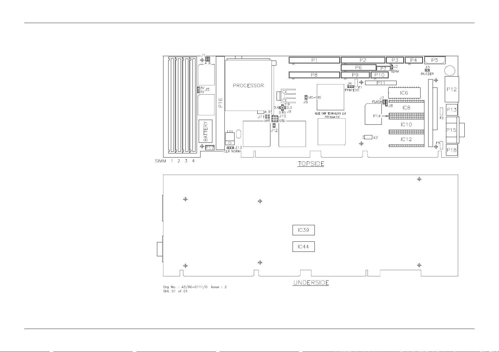
PX1 USER MANUAL PAGE 83
BOARD LAYOUT
Blue Chip Technology Ltd. 127-172
 Loading...