

Page 1

DX1
Single Board Computer
User Manual
Page 2

Page 3

DX1
User Manual
Document Part N° 0127-0173
Document Reference DX\..\0127-0173.doc
Document Issue Level 2.0
Manual covers PCBs identified Issue 2.x & 3.x (x is any digit)
All rights reserved. No part of this publication may be reproduced, stored in any retrieval system, or
transmitted, in any form or by any means, electronic, mechanical, photocopied, recorded or
otherwise, without the prior permission, in writing, from the publisher. For permission in the UK
contact Blue Chip Technology.
Information offered in this manual is correct at the time of printing. Blue Chip Technology accepts
no responsibility for any inaccuracies. This information is subject to change without notice.
All trademarks and registered names acknowledged.
Blue Chip Technology Ltd.
Chowley Oak, Tattenhall
Chester, Cheshire
CH3 9EX
Telephone : 01829 772000 Facsimile : 01829-772001
Page 4

Amendment History
Issue
Level
1.7
1.8 06/06/95 MM
1.9 04/06/96 EGW Added EMC information to Technical
2.0 11/04/96 EGW Minor corrections. New frequency
Issue
Date
11/05/95
Author Amendment Details
PMD Corrections to Version 1.6
Video Driver Information added
(ECN95/079)
Section (ECN96/060). Update to J13 link
selection for 9054 & 9154 frequency
synthesisers (ECN 96/107). External
battery voltage modified (was 3.6 V). New
front sheet. Previous filename was
DXMAN1_9.doc
synthesiser jumper settings (J13) for Iss 3
PCBs. Solid State Disk section updated.
ECN97/011 refers.
Page 5

Contents
INTRODUCTION...............................................................................................1
SPECIFICATION............................................................................................... 3
ON-BOARD FEATURES............................................................................................ 3
MEMORY OPTIONS.................................................................................................5
POWER REQUIREMENT........................................................................................... 6
ELECTROMAGNETIC COMPATIBILITY......................................................................6
ENVIRONMENT.......................................................................................................8
EMC SPECIFICATION ............................................................................................. 8
PHYSICAL............................................................................................................... 8
BIOS..................................................................................................................... 9
System BIOS......................................................................................................9
Video BIOS......................................................................................................10
Keyboard BIOS ............................................................................................... 10
Expansion ROMs.............................................................................................10
AMI HI-FLEX SYSTEM BIOS...............................................................................11
Features .......................................................................................................... 11
Hot Keys..........................................................................................................11
AMIBIOS Power-on Self Test..........................................................................12
POST Error Messages and Beep Codes.......................................................... 12
AMIBIOS SET-UP ............................................................................................... 13
Standard CMOS Set-up ...................................................................................13
Advanced CMOS Set-up.................................................................................. 13
Advanced Chipset Set-up.................................................................................13
Dx-1 Extended Set-up......................................................................................13
Utilities............................................................................................................13
Running the AMIBIOS Set-up .........................................................................14
Accessing Set-up.............................................................................................. 14
Set-up Key Use................................................................................................15
Using the CMOS Set-up Program...................................................................17
Date.................................................................................................................19
Time................................................................................................................. 19
Floppy Disk Configuration.............................................................................. 19
Hard Disk Configuration ................................................................................19
Display ............................................................................................................19
Keyboard.........................................................................................................19
Using the Advanced CMOS Set-up..................................................................20
Help Screens....................................................................................................21
Typematic Rate Programming, Typematic Rate Delay and Typematic Rate ..21
Above 1MB Memory Test ................................................................................21
Blue Chip Technology Ltd 01270173.doc
Page 6

Contents
Memory Test Tick Sound .................................................................................21
Memory Parity Error Check............................................................................21
Hit <DEL> Message Display..........................................................................21
Hard Disk Type 47 RAM Area.........................................................................22
Wait for <F1> If any Error.............................................................................22
System Boot Up Num Lock ..............................................................................22
Numeric Processor Test...................................................................................22
Floppy Drive Seek at Boot...............................................................................22
System Boot Up Sequence................................................................................23
External Cache Memory..................................................................................23
Internal Cache Memory...................................................................................23
Turbo Switch Function ....................................................................................23
Fast Gate A20 Option......................................................................................23
Password Checking Option .............................................................................24
ROM Shadow...................................................................................................24
Boot Sector Virus Protection...........................................................................24
Using the Advanced Chipset............................................................................25
Using the DX-1 Extended Set-up .....................................................................34
Programming Option.......................................................................................34
On-Board Floppy Drive...................................................................................35
On-Board IDE Drive .......................................................................................35
First Serial Port Address.................................................................................35
Second Serial Port Address .............................................................................35
Parallel Port Address ......................................................................................35
Parallel Port Mode..........................................................................................36
IRQ Active State ..............................................................................................36
First Serial Port Mode.....................................................................................36
First Serial Port 485 Mode..............................................................................36
Second Serial Port Mode.................................................................................36
Second Serial Port 485 Mode..........................................................................36
Quick Disk Boot Rom ......................................................................................36
SSD Boot Rom .................................................................................................36
CardTrick Boot Rom........................................................................................37
BIOS Extensions ..............................................................................................37
Auto Configuration with Defaults....................................................................37
Change Passwords ..........................................................................................37
Bypassing Password Support ..........................................................................37
Enabling Password Support ............................................................................37
If a Password is Used ......................................................................................37
Password Storage............................................................................................38
Password Options Control Prompt..................................................................38
Using a Password............................................................................................38
01270173.doc Blue Chip Technology Ltd
Page 7

Contents
Auto Detect Hard Disk....................................................................................38
Write to CMOS and Exit.................................................................................. 39
Do Not Write to CMOS and Exit .....................................................................39
DX1 PERIPHERAL COMPONENTS ............................................................ 40
VIDEO .................................................................................................................. 40
IBM Standard Video Modes ............................................................................41
Cirrus Logic Extended Video Modes...............................................................41
VIDEO DRIVERS ...................................................................................................42
VIDEO DRIVER INSTALLATION INSTRUCTIONS....................................................... 42
WATCHDOG TIMER .............................................................................................. 43
E²PROM..............................................................................................................43
SERIAL PORTS ......................................................................................................44
BYTE WIDE SSD USER SOCKETS.........................................................................45
BATTERY ............................................................................................................. 46
MEMORY MAP .....................................................................................................47
Typical Memory Map for a 1MByte DX1 ........................................................47
DISK DRIVES........................................................................................................48
Floppy Drives..................................................................................................48
Hard Drives (IDE) ......................................................................................... 49
HARD DISK TYPES ............................................................................................... 49
ISA BUS & VESA LOCAL BUS DETAILS ...................................................51
ISA BUS SIGNAL DESCRIPTIONS ..........................................................................51
VESA LOCAL BUS............................................................................................... 56
Description......................................................................................................56
VL-Bus Signal Definitions............................................................................... 56
BCT DX1 SBC I/O ADDRESS MAP.....................................................................61
INTERRUPT ASSIGNMENTS ................................................................................... 62
DMA ASSIGNMENTS............................................................................................ 62
APPENDIX A....................................................................................................63
POST ERROR CODES...........................................................................................63
APPENDIX B ....................................................................................................67
CONFIGURATION JUMPERS ................................................................................... 67
APPENDIX C....................................................................................................69
CONNECTOR DETAILS .......................................................................................... 69
P1: FLOPPY (34 WAY HEADER) ............................................................................ 69
P2: HARD DRIVE (40 WAY HEADER)....................................................................70
P3: COM 2 (10 WAY HEADER)..............................................................................70
Blue Chip Technology Ltd 01270173.doc
Page 8

Contents
P4: RS422/485 SERIAL (10 WAY HEADER)...........................................................71
P5: PARALLEL (26 WAY HEADER).........................................................................71
P6: FEATURE (26 WAY HEADER) ..........................................................................72
P7: VIDEO (15 WAY CONDENSED D TYPE)............................................................72
P8: POST (12 WAY HEADER).................................................................................72
P9: MOUSE (6 PIN MINI DIN)................................................................................73
P10: SSD CONNECTOR (8 WAY HEADER).............................................................73
P11: COM 1 (9 WAY D) ........................................................................................73
P12: PERIPHERAL (20 WAY HEADER)...................................................................73
P13: KEYBOARD (6 PIN MINI DIN) .......................................................................74
P14: BATTERY (4 WAY HEADER)..........................................................................74
P15: BACKPLANE UTILITY CONNECTOR (10 WAY HEADER) .................................74
P16: AT EXPANSION CONNECTOR .......................................................................75
P17: PC/XT EXPANSION CONNECTOR .................................................................76
ISA BUS XT CONNECTIONS.................................................................................77
ISA BUS AT CONNECTIONS.................................................................................78
VESA LOCAL BUS CONNECTOR ..........................................................................79
(MCA STYLE GOLD EDGE CONNECTOR)................................................................79
APPENDIX D.....................................................................................................81
CMOS RAM MAP ...............................................................................................81
APPENDIX E.....................................................................................................89
CHIPSET REGISTERS..............................................................................................89
APPENDIX F.....................................................................................................93
SOLID STATE DISK OPERATION (SSD)..................................................................93
Quick Disk SSD ...............................................................................................93
Programming the Flash...................................................................................93
Programming the SRAM..................................................................................94
DAUGHTER BOARD SSD.......................................................................................95
APPENDIX G ....................................................................................................96
CONNECTOR AND JUMPER LINK PCB POSITIONS..................................................96
01270173.doc Blue Chip Technology Ltd
Page 9

Introduction Page 1
INTRODUCTION
This manual describes the Blue Chip Technology (BCT) DX1 processor card.
There are several versions of the card; these will be identified where appropriate.
We strongly recommend that you study this manual carefully before attempting to
change the configuration. Whilst all necessary information is available in this
manual we would recommend that, unless you are confident, you contact your
supplier to effect any changes. This card uses the UMC 82C491 & 82C493 VLSI
devices, they provide a complete AT compatible environment with VESA
VL-Bus ä compatible local bus support.
WARNING
The devices on this card can be fatally damaged by static electricity. Ensure that
you touch a suitable ground to discharge any static build up before touching the
card. This should be repeated if the handling is for any length of time.
Information offered in this manual is correct at the time of printing. Blue Chip
Technology accept no responsibility for any inaccuracies. This information is
subject to change without notice.
If this product proves to be defective, Blue Chip Technology is only obliged to
replace or refund the purchase price at Blue Chip Technology's discretion.
Please contact our Customer Support Department for assistance.
Blue Chip Technology Ltd 01270173.doc
Page 10

Page 2 Introduction
Limitations of Liability
In no event shall Blue Chip Technology be held liable for any loss, expenses or
damages of any kind whatsoever, whether direct, indirect, incidental or
consequential, arising from the design or use of this product or the support
materials supplied with this product.
Trademarks
IBM, PC, AT and PS/2 are trademarks of International Business Machines
Corporation.
AMI Hi-Flex BIOS is a trademark of American Megatrends Inc.
Intel is a registered trademark of Intel Corporation
80486SX, 80486DX are registered trademarks of the Intel Corporation
VESA VL-Bus is a registered trademark of the Video Electronics Standards
Association.
01270173.doc Blue Chip Technology Ltd
Page 11

Specification Page 3
SPECIFICATION
The BCT DX1 CPUs are single slot high performance computers that provide
100% IBM PC/AT compatibility. They offer the very highest level of integration
currently available on an AT plug-in card.
In addition they support on board VL-Bus SVGA controller and will support up
to two additional VL-Bus expansion slot.
On-board Features
· Choice of 25MHz 80486SX, 33MHz 80486DX, 66MHz 80486DX2,
80486DX4/100 or P24T microprocessor
· Optional 256K Direct mapped (one way set associative) write back cache
memory with software control via set-up menu
· Up to 64MB of DRAM memory, supports 1MB x 36, 4MB x 36, 8MB x 36
and 16MB x 36 SIMM modules
· High performance memory Page Interleave access
· AMI BIOS with built in set-up program
· Hardware EMS support (LIM 3.2 & 4.0 compatible)
· Selectable Shadow RAM for system & video BIOS
· Selectable Bus speed
· Automatic or Manual Peripheral Configuration
· Local bus SVGA controller with GUI accelerator and up to 2MB of video
memory & VESA VL-bus connector
· On board optional solid state disk up to 2 MBytes of flash and 512K bytes of
battery backed SRAM
· I.D.E. controller (2 drives)
· Floppy controller (Intel 8272 compatible) supporting 360KB, 720KB,
1.2MB, 1.44MB & 2.88MB drives
· 2 asynchronous serial ports (16C550 compatible) software selectable as
RS232C or RS485 (selectable as either full or half duplex)
· Bi-directional parallel port
· AT compatible keyboard port
· PS/2 Mouse port (check configuration)
· Customer "sign-on" information held in EEPROM
· POST header
· Software selectable Watchdog timer
· On-board "Power Good" generation
· On-board speaker with additional external drive circuitry
Blue Chip Technology Ltd 01270173.doc
Page 12

Page 4 Specification
· On-board Lithium battery
· Multi layer PCB using Surface Mount Technology (SMT)
The DX1 can support memory configurations from 1MB up to 64MB. This is
achieved by offering 4, 72 pin SIMM carriers that can take modules in size from
256K x 36 bits data and (32, 4 parity bits) to 16MB x 36 bits.
The DX board can also accommodate SIMM units without parity. However
please ensure that the BIOS is set correctly for this condition.
The following table shows the memory configurations supported by the DX1.
Always ensure that you observe full static precautions before attempting to
handle the DX1 and memory modules.
01270173.doc Blue Chip Technology Ltd
Page 13

Specification Page 5
Memory Options
Option Bank 0 Bank 1 Bank 2 Bank 3 Total DRAM
1 256K - - - 1MB
2 256K 256K - - 2MB
3 256K 256K 256K - 3MB
4 256K 256K 256K 256K 4MB
5 1M - - - 4MB
6 1M 256K - - 5MB
7 1M 256K 256K - 6MB
8 1M 256K 256K 256K 7MB
9 1M 1M - - 8MB
10 1M 1M 256K - 9MB
11 1M 1M 256K 256K 10MB
12 1M 1M 1M - 12MB
13 1M 1M 1M 256K 13MB
14 1M 1M 1M 1M 16MB
15 4M - - - 16MB
16 4M 256K - - 17MB
17 4M 256K 256K - 18MB
18 4M 256K 256K 256K 19MB
19 4M 1M - - 20MB
20 4M 1M 256K - 21MB
21 4M 1M 256K 256K 22MB
22 4M 1M 1M - 24MB
23 4M 1M 1M 256K 25MB
24 4M 1M 1M 1M 28MB
25 4M 4M - - 32MB
26 4M 4M 256K - 33MB
27 4M 4M 256K 256K 34MB
28 4M 4M 1M - 36MB
29 4M 4M 1M 256K 37MB
30 4M 4M 1M 1M 40MB
31 4M 4M 4M - 48MB
32 4M 4M 4M 256K 49MB
33 4M 4M 4M 1M 52MB
34 4M 4M 4M 4M 64MB
35 16M - - - 64MB
Note:
· The four banks are made up of four 72 pin SIMM carriers
· All SIMMs must have an access time of 70ns or faster
(e.g. 60ns)
· All SIMMs modules quoted above are 32 bits wide (4 bytes)
· SIMMs modules without parity can be used with the BIOS set accordingly
Blue Chip Technology Ltd 01270173.doc
Page 14

Page 6 Specification
Power Requirement
The DX1 requires +5Vdc only. The actual current consumption varies with
configuration. The following table should be used as a guideline to the total
power requirement.
CPU Option Speed Typical Current
486SX 25 MHz 2.8A
486DX 33 MHz 3.0A
486DX2 66 MHz 3.7A
486DX4 100 MHz Contact BCT
All the above requirements are for DX1 configurations fitted with 4MB of
DRAM.
Electromagnetic Compatibility
This product meets the requirements of the European EMC Directive
(89/336/EEC) and is eligible to bear the CE mark.
It has been assessed operating in a Blue Chip Technology Icon industrial PC.
However, because the board can be installed in a variety of computers, certain
conditions have to be applied to ensure that the compatibility is maintained. It
meets the requirements for an industrial environment (Class A product) subject to
those conditions.
· The board must be installed in a computer system which provides screening
suitable for the industrial environment.
· Any recommendations made by the computer system manufacturer/supplier
must be complied with regarding earthing and the installation of boards.
· The board must be installed with the backplate securely screwed to the
chassis of the computer to ensure good metal-to-metal (i.e. earth) contact.
· Most EMC problems are caused by the external cabling to boards. It is
imperative that any external cabling to the board is totally screened, and that
the screen of the cable connects to the metal end bracket of the board and
hence to earth. It is recommended that round screened cables with a braided
wire screen are used in preference to those with a foil screen and drain wire.
Use metal connector shells which connect around the full circumference of
01270173.doc Blue Chip Technology Ltd
Page 15

Specification Page 7
the screen; they are far superior to those which earth the screen by a simple
“pig-tail”.
· The keyboard will play an important part in the compatibility of the processor
card since it is a port into the board. A fully compatible keyboard must be
used otherwise the keyboard itself may radiate or behave as if keys are
pressed when subject to interference. Under these circumstances it may be
beneficial to add a ferrite clamp on the keyboard lead as close as possible to
the connector. A suitable type is the Chomerics type H8FE-1004-AS.
· Ensure that the screens of any external cables are bonded to a good RF earth
at the remote end of the cable.
Failure to observe these recommendations may invalidate the EMC compliance.
Warning
This is a Class A product. In a domestic environment this product
may cause radio interference in which case the user may be
required to take adequate measures.
Blue Chip Technology Ltd 01270173.doc
Page 16

Page 8 Specification
Environment
Operating Temperature 0°C to 60°C.
Storage Temperature -20°C to 70°C.
Relative Humidity 90% non-condensing.
EMC Specification
A Blue Chip Technology Icon industrial PC fitted with this card meets the
following specification:
Emissions EN 55022:1995
Radiated Class A
Conducted Class A & B
Immunity EN 50082-2:1995 incorporating:
Electrostatic Discharge IEC 801-2:1991
Performance Criteria A
Radio Frequency Susceptibility ENV 50140:1993
Performance Criteria A
Fast Burst Transients IEC 801-4:1988
Performance Criteria A
Physical
Size 339 x 122mm
Occupies one AT/VESA slot
01270173.doc Blue Chip Technology Ltd
Page 17

BIOS Page 9
BIOS
Overview
There are several types of Basic Input Output Systems (BIOS) in a PC system.
System BIOS
This controls the local electronics. It also provides the interface to the hardware
for the operating system.
Video BIOS
This controls the interface between the video hardware and the computer.
Keyboard BIOS
This controls the keyboard matrix operation, interacts with switches, LEDs, etc.
and communicates with the PC.
Each of these BIOS's will now be described :
System BIOS
The primary function of the System BIOS is to provide a series of software
interrupts, functions and sub functions that perform specific system tasks; such as
writing or reading to and from disks and video screens.
The operating system uses the System BIOS as the route to communicate and
control the microprocessor and its immediate peripherals. This exchange of data
occurs via a strict protocol .
The secondary function of the System BIOS is the series of tests and
initialisations that occur after power-on. The results of these operations are
written to the POST display (if fitted) as they are completed, thereby indicating
its progress.
Blue Chip Technology Ltd 01270173.doc
Page 18

Page 10 BIOS
The System BIOS on the DX1 is contained in a 128KB EPROM; of this space
the System BIOS occupies 64KB. The EPROM is located at address F0000 hex
and continues to FFFFF hex. The supplier of the BIOS is AMI, currently the
leading supplier of PC BIOS's in the world. BCT have selected this supplier
because of their experience, support and commitment to future developments in
this critical area of a PC/AT design.
Video BIOS
The Video BIOS acts as an interface between the System BIOS and the video
hardware. It is critical that this interface is compatible, fast and reliable. The
Video BIOS provides a relatively high level of access to the hardware. The onboard video hardware on the DX1 is based on the Cirrus Logic
GD5424/26/28/29. This device offers proven VGA compatibility as well as
providing enhanced GUI acceleration in a single device. It is supported by up to
2MB of video memory. The Video BIOS co-exists in the System BIOS EPROM
but locates in the address range C0000 to C7FFF hex.
Keyboard BIOS
The Keyboard BIOS is contained in the 8042 (or 8742) keyboard controller. This
device provides a parallel interface to the microprocessor bus allowing a bidirectional streams of data to be passed between the PC and the keyboard. The
BIOS is programmed into the 8042. It occupies none of the memory map.
Expansion ROMs
Most PCs allow add-on cards to be inserted into the backplane. If software is
required to control the electronics on the card the supplier may choose to provide
this software in the form of an expansion ROM or adapter ROM. On power-on
the PC, once initialised, checks for the presence of ROMs within the memory
space of C8000 to DFFFF hex. If present the code within the ROM is run and the
specific hardware on the card controlled accordingly. In addition this software
can then be used as the interface to the electronics by the operating system;
thereby acting as an extension to the System BIOS for the new electronics.
01270173.doc Blue Chip Technology Ltd
Page 19

BIOS Page 11
AMI Hi-Flex System BIOS
Features
· Keyboard Speed Switching
· Enable Cache Memory
· Memory Detection
· Password Support
· Auto detection of IDE Hard Drive Parameters
· Auto detection of Processor Type and Speed
· Auto detection of Memory Size and Type
· Customisation of the System
· User definable Hard Disk Types
· PS/2 Mouse Support
· Boot Sector Virus Support
· Local Peripheral Support
· Shadow RAM Support
· Keyboard Typematic Rate and Delay
· Num Lock Power-on Status
· Fast Gate A20 Support
Hot Keys
The Hi-Flex AMIBIOS provides hot keys to switch speed and cache operation.
These key operations are:
<Ctrl>,<Alt> and <+> Selects High Speed
<Ctrl>,<Alt> and <-> Selects Low Speed
<Ctrl>,<Alt>,<Shift> and <+> Enables External Cache
<Ctrl>,<Alt>,<Shift> and <-> Disables External Cache
<Ctrl>,<Alt> and <DEL> Causes a Soft Reset
All keys should be pressed together.
Blue Chip Technology Ltd 01270173.doc
Page 20

Page 12 BIOS
AMIBIOS Power-on Self Test
The Hi-Flex AMIBIOS provides all IBM standard POST routines as well as
enhanced AMIBIOS routines. All POST checkpoint codes are written to the
POST display at I/O location 80 hex (if fitted). See the POST error codes
Appendix A.
POST Error Messages and Beep Codes
If the BIOS cannot configure the display controller it will communicate the
identification of fatal errors (except error code 8) via a series of beeps. These
errors will only occur during power-on tests. The beep codes are as follows:
Beeps Error Messages Description
1 Refresh Failure Memory Refresh circuitry faulty.
2 Parity Error Parity error in the first 64KB of memory.
3 Base 64KB Memory Failure. Memory failure in the first 64KB.
4 Timer not Operational. Timer 1 is not functioning. Alternatively,
5 Processor error. CPU error.
6 8042 - Gate A20 Failure. BIOS cannot switch to protected mode.
7 Processor Exception Interrupt
Error.
8 Display Memory Read/Write
Error.
9 ROM Checksum Error. ROM checksum embedded in the ROM
10 CMOS Shutdown Register
Read/Write Error.
11 Cache Memory Bad - Do Not
Enable Cache
memory in the first 64KB faulty.
CPU generated an exception interrupt
error.
Video adapter is not responding or its
memory is faulty.
does not match the calculated value.
The shutdown register in the CMOS
RAM failed. Check access to CMOS.
The cache memory test failed. Cache
memory is disabled. Do not press
<CTRL> <ALT> <SHIFT> <+> to enable
cache memory.
What to do if the DX1 Beeps
If the system beeps...... then....
1,2 or 3 times Re-seat the SIMMs. If the DX1 still
beeps, replace the SIMMs checking the
access time.
6 times Check the keyboard connections. If the
beeps persist change the keyboard.
4,5,7,8,9,10 or 11 Contact Blue Chip Technology
01270173.doc Blue Chip Technology Ltd
Page 21

BIOS Page 13
AMIBIOS Set-up
The Hi-Flex AMIBIOS Set-up utility is divided into five parts:
Standard CMOS Set-up
The Hi-Flex AMIBIOS Standard CMOS Set-up permits the user to configure and
set system components such as floppy drives, hard disk drives, time and date,
monitor type and keyboard. These options are discussed on page 17.
Advanced CMOS Set-up
The Advanced CMOS Set-up allows the user to configure more advanced parts
of memory operation and peripheral support. These options are discussed on
page 20.
Advanced Chipset Set-up
The Advanced Chipset configures the UMC 82C491 specific features and is
discussed further on page 25.
Dx-1 Extended Set-up
The DX-1 Extended Set-up configures the on-board floppy, IDE, serials and
parallel devices. These are all controlled by the SMC 37C663 device. In addition
it provides configuration of the Quick Disk SSD and Daughter Board SSD
facilities. These options are discussed further on page 34.
Utilities
The AMIBIOS provides support for Password security access. This will be
discussed further on page 37.
Blue Chip Technology Ltd 01270173.doc
Page 22

Page 14 BIOS
Running the AMIBIOS Set-up
The system parameters (such as amount of memory, disk drives, video displays
and numeric co-processors) are stored in CMOS RAM. When the DX1 is turned
off, a back-up battery on-board the DX1 provides power to the CMOS RAM,
thereby retaining the system parameters.
Each time the DX1 is powered-on, it is configured with these values, unless the
CMOS RAM has been corrupted. The AMIBIOS Set-up resides in the ROM
BIOS and is available each time the DX1 is switched on.
If, for some reason, the CMOS RAM becomes corrupted, the system is re
configured with the default values stored in the System BIOS. There are two sets
of BIOS values stored in the BIOS: the BIOS default values and the Power-On
default values.
The Power-on default settings consist of the safest set of parameters. These
settings should be used if the system is behaving erratically. They should work in
the majority of cases but do not provide optional system performance
characteristics.
Accessing Set-up
Set-up is accessed by pressing the 'DEL' key on the keyboard when the screen
displays the message:
Hit <DEL> if you want to run Set-up
If you press 'DEL' too late, reset the DX1 and try again.
01270173.doc Blue Chip Technology Ltd
Page 23

BIOS Page 15
Set-up Key Use
Keystroke Action
Esc Returns to the previous screen.
®,¬,% and ¯
<PgUp> and
<PgDn>,
<Ctrl><PgUp>,
<Ctrl><PgDn>
<F1> Displays help.
<F2> Changes background colours.
<F3> Changes foreground colours.
<F5> Restores the values resident when the current Set-up session began.
<F6> Loads all features in the Advanced CMOS Set-up/Advanced Chipset
<F7> Loads all features in the Advanced CMOS Set-up/Advanced Chipset
<F10> Saves all the changes made to Set-up and continues the boot process.
Move the cursor from one option to the next.
Modify the default value of the options for the highlighted parameter.
If there are fewer than 10 options, <Ctrl><PgUp> and <Ctrl><PgDn>
operate like <PgUp> and <PgDn>.
<Ctrl> can also be used to increment a setting.
These values are taken from the CMOS RAM if it was uncorrupted at
the start of the session. Otherwise, the AMIBIOS Set-up default values
are used.
Set-up with the AMIBIOS Set-up defaults.
with the Power-On defaults.
The DX1 AMIBIOS Set-up main Menu is shown below. The options are selected
by using the % and ¯ keys and then pressing <Enter> .
AMIBIOS SET-UP PROGRAM - BIOS SET-UP UTILITIES
Copyright 1993 (c) American Megatrends, Inc. All Rights Reserved
STANDARD CMOS SET-UP
ADVANCED CMOS SET-UP
ADVANCED CHIP SET SET-UP
AUTO CONFIGURATION WITH BIOS DEFAULTS
AUTO CONFIGURATION WITH POWER ON DEFAULTS
Standard CMOS Set-up for changing Time, Date, Hard Disk Type, etc.
Blue Chip Technology Ltd 01270173.doc
DX-1 EXTENDED SET-UP
PERIPHERAL SET-UP
CHANGE PASSWORD
AUTO DETECT HARD DISK
HARD DISK UTILITY
WRITE TO CMOS AND EXIT
DO NOT WRITE TO CMOS AND EXIT
Page 24

Page 16 BIOS
Each option is described in detail on the pages identified as follows:
Main Menu Option Described on Page
STANDARD CMOS SET-UP
ADVANCED CMOS SET-UP
ADVANCED CHIP SET SET-UP
DX-1 EXTENDED SET-UP
AUTO CONFIGURATION WITH BIOS DEFAULTS
AUTO CONFIGURATION WITH POWER ON DEFAULTS
CHANGE PASSWORD
AUTO DETECT HARD DISK
HARD DISK UTILITY
WRITE TO CMOS AND EXIT
DO NOT WRITE TO CMOS AND EXIT
17
20
25
34
37
37
37
38
39
39
01270173.doc Blue Chip Technology Ltd
Page 25

BIOS Page 17
Using the CMOS Set-up Program
The default condition for the CMOS Set-up Menu is as shown below. This menu
sets the basic system parameters, such as date, time, floppy disk and hard disk
types. By using the ¬%¯® keys you can select the parameter to be changed.
Once positioned on the parameter to be modified the <PgUp> and <PgDn> keys
rotate the available options. The value selected when the menu is exited is the
one that will be written to CMOS, should you decide to commit your changes to
CMOS.
ЙННННННННННННННННННННННННННННННННННННННННННННН
º AMIBIOS SETUP PROGRAM - STANDARD CMOS SETUP º
º (C)1993 American Megatrends Inc., All Rights Reserved º
МННННННННННННННННННННННННННННННННННННННННННННН
º º
º Date (mn/date/year): Tue, Jan 01 1980 Base Memory : 640KB º
º Time (hour/min/sec): 00 : 00 : 00 Ext. Memory : 4096 KB º
º Cyln Head WPcom LZone Sect Size º
º Hard Disk C: Type : Not Installed º
º Hard Disk D: Type : Not Installed º
º Keyboard : Installed º 30³ 31³ 1³ 2³ 3³ 4³
º º 6³ 7³ 8³ 9³ 10³ 11³
ЙННННННННННННННННННННННННННННННННННННННННННННН
º º Date : 01, 02, 03,...31 º º 20³ 21³ 22³ 23³ 24³ 25³
ИННННННННННННННННННННННННННННННННННННННННННННН
º º 3³ 4³ 5³ 6³ 7³ 8³
ННННННННННННННННННННННННННННННННН»
ННННННННННННННННННННННННННННННННН¹
º Floppy Drive A: : 1.44 MB, 3 «"
ЙНННСНННСНННСНННСНННСНННСННН¹
º Floppy Drive B: : Not Installed
ºSun³Mon³Tue³Wed³Thu³Fri³Satº
º Primary Display : VGA/PGA/EGA
МНННШНННШНННШНННШНННШНННШННН¹
5º
º
ЗДДДЕДДДЕДДДЕДДДЕДДДЕДДДЕДДД
12º
º
ЗДДДЕДДДЕДДДЕДДДЕДДДЕДДДЕДДД
º
Í» º 13³ 14³ 15³ 16³ 17³ 18³ 19º
º º Month : Jan, Feb,.....Dec º
ЗДДДЕДДДЕДДДЕДДДЕДДДЕДДДЕДДД
26º
º º Year : 1901, 1902,...2099 º
ЗДДДЕДДДЕДДДЕДДДЕДДДЕДДДЕДДД
º
ͼ º 27³ 28³ 29³ 30³ 31³ 1³ 2º
º
ЗДДДЕДДДЕДДДЕДДДЕДДДЕДДДЕДДД
9º
Blue Chip Technology Ltd 01270173.doc
Page 26

Page 18 BIOS
ȵ ESC:Exit ¯®%¬:Select F2/F3:Color PU/PD:Modify
ЖКНННПНННПНННПНННПНННПНННПННН¼
01270173.doc Blue Chip Technology Ltd
Page 27

BIOS Page 19
Date
This entry allows you to set the Date, Month and Year. Ranges for each value
are shown in the lower left corner of the CMOS Set-up Screen.
Time
This entry allows you to set the Hours, Minutes and Seconds. The clock operates
in 24 hour mode; that means that for a PM time add 12 to the hour
e.g. enter 6:35 PM as 18:35:00.
Floppy Disk Configuration
The DX1 supports None, 360KB, 720KB, 1.2MB, 1.44MB & 2.88MB drives.
The BIOS supports two drives A: and B:
Hard Disk Configuration
Two hard disk drives are supported directly by the BIOS, C: and D:. Each drive
can select drive types from 1 to 46. In addition type 47 is user definable allowing
customised parameters for the drive to be entered. Both drives can be set to a
different type 47 if required. To set the values for type 47 use the ¬,%,¯ and ®
keys to select the appropriate field and then type in as required. A complete list
of the 46 hard disk type is contained in the Technical Reference section of this
manual on page 49.
Display
This entry allows the user to select MDAä (monochrome), CGAä or
EGA/PGA/VGA display controllers.
If your system is to operate without a display then select Disabled. Failure to do
this will result in an error being generated during the power-on diagnostics check.
Keyboard
The DX1 keyboard interface can be connected to either AT or PS/2 keyboards.
The default setting is Enabled. If your system is to operate without a keyboard
then select Disabled. Failure to do this will result in an error being generate
during the power-on diagnostics check.
Blue Chip Technology Ltd 01270173.doc
Page 28

Page 20 BIOS
Using the Advanced CMOS Set-up
The default condition for the Advanced CMOS Set-up Menu is as shown below.
By using the ¬%¯® keys you can select the parameter to be changed. Once
positioned on the parameter to be modified the <PgUp> and <PgDn> keys rotate
the available options. The value selected when the menu is exited is the one that
will be written to CMOS, should you decide to commit your changes to CMOS.
ЙННННННННННННННННННННННННННННННННННННННННННННН
º AMIBIOS SETUP PROGRAM - ADVANCED CMOS SETUP º
º (C)1993 American Megatrends Inc., All Rights Reserved º
МННННННННННННННННННННННННННННННННННННННЛНННННН
º Typematic Rate Programming : Enabled º BootSector Virus Protection: Disabled º
º Typematic Rate Delay (msec): 500 º CPU Internal Clock Mode : 1X º
º Typematic Rate (Chars/Sec) : 30 º IDE Block Mode Transfer : Disabled º
º Above 1 MB Memory Test : Disabled º IDE Standby mode : Disabled º
º Memory Test Tick Sound : Enabled º Auto Key-Lock Timeout : Disabled º
º Memory Parity Error Check : Enabled º º
º Hit <DEL> Message Display : Enabled º º
º Hard Disk Type 47 RAM Area : 0:300 º º
º Wait For <F1> If Any Error : Enabled º º
º System Boot Up Num Lock : On º º
º Numeric Processor Test : Enabled º º
º Weitek Processor : Absent º º
º Floppy Drive Seek At Boot : Enabled º º
º System Boot Up Sequence : A:, C: º º
º System Boot Up CPU Speed : High º º
º External Cache Memory : Enabled º º
º Internal Cache Memory : Enabled º º
º Password Checking Option : Setup º º
МННННННННННННННННННННННННННННННННННННННКНННННН
ННННННННННННННННННННННННННННННННН»
ННННННННННННННННННННННННННННННННН¹
ННННННННННННННННННННННННННННННННН¹
МННННННµ ESC:Exit ¬%®¯:Sel (Ctrl)Pu/Pd:Modify F1:Help F2/F3:Color
ЖННННННН¹
ИНННННННµ F5:Old Values F6:BIOS Setup Defaults F7:Power-On Defaults
ЖННННННН¼
01270173.doc Blue Chip Technology Ltd
Page 29

BIOS Page 21
Help Screens
Help can be invoked at any time by pressing <F1>.
Typematic Rate Programming, Typematic Rate Delay and Typematic Rate
The control of Typematic Rate Programming allows the auto repeat and delay
before repeat to be selected. The defaults are as shown above. The Typematic
Rate Delay describes the delay before auto repeat starts. The Typematic Rate is
the frequency of the key generation once in auto repeat.
Above 1MB Memory Test
By enabling this test any RAM above 1MB will be exercised by the POST
diagnostics thereby taking longer to boot. If your DX1 is not fitted with more
than 1MB of RAM or you wish to shorten the boot time set this option to
disabled. If you wish to ensure maximum DRAM integrity then set this option to
Enabled.
Memory Test Tick Sound
This option selects whether an audible indication of the presence of memory
during the POST is generated or not. Once either <ESC> or <DEL> is depressed
the audio is disabled
Memory Parity Error Check
This option selects whether the parity circuit is active on the system RAM. We
strongly recommend that this is set to enabled at all times thereby providing
communication of any RAM corruption. If this option is not required select
disabled. This option must be set if you are using SIMM units without parity bits
i.e. 32 bits wide.
Hit <DEL> Message Display
Disabling this option removes this message prompt from appearing during
power-up. This may be required when you do not wish to draw attention to
existence of the Setup Menus within the BIOS. The default is enabled.
Blue Chip Technology Ltd 01270173.doc
Page 30

Page 22 BIOS
Hard Disk Type 47 RAM Area
As described in the Set-up details previously the AMIBIOS supports type 47 user
definable input. This data is stored at either:
0:300h in lower system RAM
or
The top 1KB of applications memory
If the latter is selected the information will be stored in shadow RAM if
shadowing is enabled.
Wait for <F1> If any Error
If any of the tests run during the POST cause an error then this message will be
displayed. If this message is enabled then after displaying it the DX1 will halt
waiting for <F1> to be pressed. If you expect errors during the POST or do not
wish the boot to be halted if any error occurs then disable this option.
System Boot Up Num Lock
If you wish the numeric keypad to be active after a boot then select ON. If,
however, you wish the ¬,%,¯ and ® keys to be available after power-up then
set this option to OFF.
Numeric Processor Test
This option enables or disables the AMIBIOS test for a maths co-processor. The
settings are Enabled or Disabled.
Floppy Drive Seek at Boot
If enabled, a seek is performed on floppy drive A: at system boot time. The
options are Enabled or Disabled. By disabling this option the boot time can be
reduced. If very old 360KB drives are used it may be necessary to enable this
option to ensure that the heads are recalibrated before any data is accessed.
01270173.doc Blue Chip Technology Ltd
Page 31

BIOS Page 23
System Boot Up Sequence
The default boot sequence is drive A: and then C:. This would mean that if drive
A: is not ready then the boot occurs from C:. The alternative is to boot from drive
C: and if C: is not ready then drive A. Hence the settings are either:
A:, C: or C:, A:.
External Cache Memory
The default is Enabled. If your DX1 is configured with external cache (256KB)
then this will then be used. The option is to Disable the cache.
Internal Cache Memory
This option enables the CPU internal cache memory. The settings are Enabled or
Disabled. The BIOS Set-up default is Enabled.
Turbo Switch Function
This option enables the externally mounted hardware Turbo switch. the settings
are Enabled or Disabled. The default is Enabled. Always ensure that a switch is
connected when the setting is Enabled so that noise does not cause false selection
of speed states.
Fast Gate A20 Option
Gate A20 controls the method of accessing memory addresses above 1 MB by
enabling or disabling access to the processor line A20. To provide XT
compatibility address line A20 must always be low and therefore the option
should be Disabled. However, some applications both enter protected mode and
shut down through the BIOS. For this software, Gate A20 must be constantly
enabled and disabled via the keyboard controller (8042), which slows down the
processing.
Fast Gate A20 is another method for handling Gate A20 using the UMC491
internal circuitry. It speeds programs that constantly change from addressing
conventional memory to addressing memory addresses above 1MB (from real
mode to protected mode and back). Network operating systems in particular
benefit from this enhanced circuitry.
Blue Chip Technology Ltd 01270173.doc
Page 32

Page 24 BIOS
Password Checking Option
This option enables a password check every time the systems boots or Set-up is
executed. The settings are Always or Set-up. If Always is selected the user
password prompt appears every time the system is turned on. If Set-up is chosen,
the password prompt appears if Set-up is executed.
ROM Shadow
ROM shadow is a technique in which the BIOS code is copied from slower ROM
to faster RAM. The BIOS is then executed from the RAM.
For each of the areas of memory identified in the Set-up table the option is there
to Enable or Disable shadowing for that particular area. The default is that both
the Video and System areas are shadowed. Care must be taken where expansion
cards are occupying an area that is set for shadowing. If the expansion card has
its own internal RAM located at the address that is shadowed then its operation
will be corrupted (examples are network cards). For such cards the setting should
be Disabled.
Boot Sector Virus Protection
When enabled, the BIOS issues a warning when any program or Virus issues a
Disk Format command or attempts to write to the boot sector of the hard disk.
The settings are Enabled or Disabled.
01270173.doc Blue Chip Technology Ltd
Page 33

BIOS Page 25
Using the Advanced Chipset
The default condition for the Advanced Chipset Set-up Menu is as shown below.
By using the ¬%¯® keys you can select the parameter to be changed. Once
positioned on the parameter to be modified the <PgUp> and <PgDn> keys rotate
the available options. The value selected when the menu is exited is the one that
will be written to CMOS, should you decide to commit your changes to CMOS.
ЙННННННННННННННННННННННННННННННННННННННННННННН
º AMIBIOS SETUP PROGRAM - ADVANCED CHIPSET SETUP º
º (C)1993 American Megatrends Inc., All Rights Reserved º
МННННННННННННННННННННННННННННННННННННННЛНННННН
º AUTO Config Function : Enabled º Memory Remapping : Enabled º
º Cache Read Option : 3-1-1-1 º F Segment Shadow RAM : Into-486 º
º Cache Write Option : 1 W.S. º E Segment Shadow RAM : Disabled º
º DRAM Type : FastPage º C000-C3FF Shadow RAM : Into-486 º
º DRAM Wait State(s) : 1 W.S. º C400-C7FF Shadow RAM : Into-486 º
º Keyboard Clock Select: CPUCLK/4 º C800-CBFF Shadow RAM : Disabled º
º AT Clock Select : CPUCLK/4 º CC00-CFFF Shadow RAM : Disabled º
º IO Recovery Time : 5/3 BCLK º D000-D3FF Shadow RAM : Disabled º
º Hold PD Bus : 1~2 T º D400-D7FF Shadow RAM : Disabled º
º Refresh Cycle : Slow º D800-DBFF Shadow RAM : Disabled º
º CoProcessor Ready : Delay 1T º DC00-DFFF Shadow RAM : Disabled º
º Check ELBA# Signal : in T2 º Refresh Divider : 1 º
º Non-Cacheable Block1 Enable: Disabled º Data Location of Local Bus : PD Bus º
º Non-Cacheable Block-1 Size : 4MB º LOWA20#,RC Emulation : Both º
º Non-Cacheable Block-1 Base : 0KB º Stretch 0WS# Signal Option : Do Not º
º Non-Cacheable Block2 Enable: Disabled º Hardware Parity Check : Enabled º
º Non-Cacheable Block-2 Size : 16MB º º
º Non-Cacheable Block-2 Base : 0KB º º
МННННННННННННННННННННННННННННННННННННННКНННННН
ННННННННННННННННННННННННННННННННН»
ННННННННННННННННННННННННННННННННН¹
ННННННННННННННННННННННННННННННННН¹
МНННННННµ ESC:Exit ¯®%¬:Sel (Ctrl)Pu/Pd:Modify F1:Help F2/F3:Color
ЖННННННН¹
ИНННННННµ F5:Old Values F6:BIOS Setup Defaults F7:Power-On Defaults
ЖННННННН¼
Blue Chip Technology Ltd 01270173.doc
Page 34

Page 26 BIOS
Auto Config Function
The settings are Auto or Manual. If this option is set to Enabled, the following
ADVANCED CHIPSET SET-UP options are automatically configured to
optimal settings by AMIBIOS based on the DX1 and CPU frequency:
Cache Read Option,
Cache Write Option,
DRAM Type,
DRAM Wait State(s),
Keyboard Clock Select,
AT Clock Select, and
IO Recovery Time of ISA/PCB.
Hold PD Bus,
Cache Read Option
The settings are 3-2-2-2, 3-1-1-1, or 2-1-1-1.
Cache Write Option
This option sets the number of wait states inserted before all write operations to
secondary cache memory. The settings are 0 W/S, 1 W/S, or 2 W/S. The BIOS
Set-up default is 1 W/S. The Power-On default is 2 W.S.
DRAM Type
This option specifies the type of DRAM used for system memory. The settings
are Page Mode or Fast Page.
DRAM Wait State(s)
This option sets the number of wait states inserted before all DRAM system
memory operations. The settings are 0 W.S., 1 W.S., or 2 W.S.
Keyboard Clock Select
This option sets the source of the keyboard clock. The settings are CPUCLK/6,
CPUCLK/5, CPUCLK/4, CPUCLK/3, CPUCLK/2, 9.5 MHz, or 7.2 MHz.
01270173.doc Blue Chip Technology Ltd
Page 35

BIOS Page 27
AT Clock Select
This option sets the source of the AT Clock (ATCLK). The settings are
CPUCLK/6, CPUCLK/5, CPUCLK/4, CPUCLK/3, CPUCLK/2, CPUCLK/8, or
7.2 MHz.
IO Recovery Time
The settings are 0/0 BCLK, 1/1 BCLK, 2/2 BCLK, 3/3 BCLK, 5/2 BCLK, 7/3
BCLK, 9/3 BCLK, 12/3 BCLK, 5/5 BCLK, 7/7 BCLK, 9/9 BCLK, or
12/12BCLK.
Hold PD Bus
The settings are 1~2 T or 2~3 T.
Refresh Cycle
The settings are Slow or Fast.
Coprocessor READY
This option sets the length of the delay of the coprocessor READY# signal. The
settings are Delay 1T or No Delay.
Check ELBA# Signal
This option sets the length of the delay before the ELBA# signal is checked. The
settings are in T1 or in T2.
Non-cacheable Block1 Enable
Non-cacheable Block2 Enable
If disabled, the contents of the specified block of system memory cannot be
written to or read from cache memory. These options permit the user to specify
an area of memory (Block-1 or Block-2) that cannot be cached. The settings are
Enabled or Disabled.
Blue Chip Technology Ltd 01270173.doc
Page 36

Page 28 BIOS
Non-cacheable Block-1 Base
Non-cacheable Block-2 Base
These options set the base address (or beginning) of areas of memory whose
contents cannot be written to or read from cache memory. The base address must
begin on a boundary equal to the Non-cacheable Block Size setting. The settings
are 0 KB through 16384 KB.
Memory Remapping
If this option is enabled, the contents of system memory between A0000h and
FFFFFh that have not been shadowed to RAM from ROM are moved to the top
of system memory. The settings are Enabled or Disabled.
E Segment Shadow RAM
This option specifies if the contents of the ROM memory segment from E0000 EFFFFh are shadowed to RAM and if these contents can be stored in cache
memory.
Setting Description
Into-486 The contents of E0000h - EFFFFFh are shadowed from ROM to
Cached The contents of E0000h - EFFFFFh are shadowed from ROM to
Disabled The contents of E0000h - EFFFFFh cannot be shadowed from
Enabled The contents of E0000h - EFFFFFh are shadowed from ROM to
RAM and can be written to or read from the internal cache
memory on the 486, but not to external (secondary) cache
memory.
RAM and can be written to or read from cache memory.
ROM to RAM and cannot be written to or read from cache
memory.
RAM but cannot be written to or read from cache memory.
01270173.doc Blue Chip Technology Ltd
Page 37

BIOS Page 29
F Segment Shadow RAM
This option specifies if the contents of the ROM memory segment from F0000 FFFFFh are shadowed to RAM and if these contents can be stored in cache
memory.
Setting Description
Into-486 The contents of F0000h - FFFFFFh are shadowed from ROM to RAM
Cached The contents of F0000h - FFFFFFh are shadowed from ROM to RAM
Disabled The contents of F0000h - FFFFFFh cannot be shadowed from ROM to
Enabled The contents of F0000h - FFFFFFh are shadowed from ROM to RAM
and can be written to or read from the internal cache memory on the
486, but not to external (secondary) cache memory.
and can be written to or read from cache memory.
RAM and cannot be written to or read from cache memory.
but cannot be written to or read from cache memory.
C000-C3FF Shadow RAM
This option specifies if the contents of the ROM memory area from C0000 C3FFFh are shadowed to RAM and if these contents can be stored in cache
memory.
Setting Description
Into-486 The contents of C0000h - C3FFFFh are shadowed from ROM to RAM
Cached The contents of C0000h - C3FFFFh are shadowed from ROM to RAM
Disabled The contents of C0000h - C3FFFFh cannot be shadowed from ROM to
Enabled The contents of C0000h - C3FFFFh are shadowed from ROM to RAM
Blue Chip Technology Ltd 01270173.doc
and can be written to or read from the internal cache memory on the
486, but not to external (secondary) cache memory.
and can be written to or read from cache memory.
RAM and cannot be written to or read from cache memory.
but cannot be written to or read from cache memory.
Page 38

Page 30 BIOS
C400-C7FF Shadow RAM
This option specifies if the contents of the ROM memory area from C4000 C7FFFh are shadowed to RAM and if these contents can be stored in cache
memory.
Setting Description
Into-486 The contents of C4000h - C7FFFFh are shadowed from ROM to RAM
Cached The contents of C4000h - C7FFFFh are shadowed from ROM to RAM
Disabled The contents of C400h - C7FFFh cannot be shadowed from ROM to
Enabled The contents of C400h - C7FFFh are shadowed from ROM to RAM
and can be written to or read from the internal cache memory on the
486, but not to external (secondary) cache memory.
and can be written to or read from cache memory.
RAM and cannot be written to or read from cache memory.
but cannot be written to or read from cache memory.
C800-CBFF Shadow RAM
This option specifies if the contents of the ROM memory area from C8000 CBFFFh are shadowed to RAM and if these contents can be stored in cache
memory.
Setting Description
Into-486 The contents of C8000h - CBFFFFh are shadowed from ROM to RAM
Cached The contents of C8000h - CBFFFFh are shadowed from ROM to RAM
Disabled The contents of C8000h - CBFFFFh cannot be shadowed from ROM
Enabled The contents of C8000h - CBFFFFh are shadowed from ROM to RAM
01270173.doc Blue Chip Technology Ltd
and can be written to or read from the internal cache memory on the
486, but not to external (secondary) cache memory.
and can be written to or read from cache memory.
to RAM and cannot be written to or read from cache memory.
but cannot be written to or read from cache memory.
Page 39

BIOS Page 31
CC00-CFFF Shadow RAM
This option specifies if the contents of the ROM memory area from CC000 CFFFFh are shadowed to RAM and if these contents can be stored in cache
memory.
Setting Description
Into-486 The contents of CC000h - CFFFFFh are shadowed from ROM to
Cached The contents of CC000h - CFFFFFh are shadowed from ROM to
Disabled The contents of CC000h - CFFFFFh cannot be shadowed from ROM
Enabled The contents of CC000h - CFFFFFh are shadowed from ROM to
RAM and can be written to or read from the internal cache memory on
the 486, but not to external (secondary) cache memory.
RAM and can be written to or read from cache memory.
to RAM and cannot be written to or read from cache memory.
RAM but cannot be written to or read from cache memory.
D000-D3FF Shadow RAM
This option specifies if the contents of the ROM memory area from D0000 D3FFFh are shadowed to RAM and if these contents can be stored in cache
memory.
Setting Description
Into-486 The contents of D0000h -D3FFFFh are shadowed from ROM to RAM
Cached The contents of D0000h - D3FFFFh are shadowed from ROM to RAM
Disabled The contents of D0000h - D3FFFFh cannot be shadowed from ROM
Enabled The contents of D0000h - D3FFFFh are shadowed from ROM to RAM
Blue Chip Technology Ltd 01270173.doc
and can be written to or read from the internal cache memory on the
486, but not to external (secondary) cache memory.
and can be written to or read from cache memory.
to RAM and cannot be written to or read from cache memory.
but cannot be written to or read from cache memory.
Page 40

Page 32 BIOS
D400-D7FF Shadow RAM
This option specifies if the contents of the ROM memory area from D4000 D7FFFh are shadowed to RAM and if these contents can be stored in cache
memory.
Setting Description
Into-486 The contents of D4000h -D7FFFFh are shadowed from ROM to RAM
Cached The contents of D4000h - D7FFFFh are shadowed from ROM to RAM
Disabled The contents of D4000h - D7FFFFh cannot be shadowed from ROM
Enabled The contents of D4000h - D7FFFFh are shadowed from ROM to RAM
and can be written to or read from the internal cache memory on the
486, but not to external (secondary) cache memory.
and can be written to or read from cache memory.
to RAM and cannot be written to or read from cache memory.
but cannot be written to or read from cache memory.
D800-DBFF Shadow RAM
This option specifies if the contents of the ROM memory area from D8000 DBFFFh are shadowed to RAM and if these contents can be stored in cache
memory.
Setting Description
Into-486 The contents of D8000h -DBFFFFh are shadowed from ROM to RAM
Cached The contents of D8000h - DBFFFFh are shadowed from ROM to
Disabled The contents of D8000h - DBFFFFh cannot be shadowed from ROM
Enabled The contents of D8000h - DBFFFFh are shadowed from ROM to
01270173.doc Blue Chip Technology Ltd
and can be written to or read from the internal cache memory on the
486, but not to external (secondary) cache memory.
RAM and can be written to or read from cache memory.
to RAM and cannot be written to or read from cache memory.
RAM but cannot be written to or read from cache memory.
Page 41

BIOS Page 33
DC00-DFFF Shadow RAM
This option specifies if the contents of the ROM memory area from DC000 DFFFFh are shadowed to RAM and if these contents can be stored in cache
memory.
Setting Description
Into-486 The contents of DC000h -DFFFFFh are shadowed from ROM to RAM
Cached The contents of DC000h - DFFFFFh are shadowed from ROM to
Disabled The contents of DC000h - DFFFFFh cannot be shadowed from ROM
Enabled The contents of DC000h - DFFFFFh are shadowed from ROM to
and can be written to or read from the internal cache memory on the
486, but not to external (secondary) cache memory.
RAM and can be written to or read from cache memory.
to RAM and cannot be written to or read from cache memory.
RAM but cannot be written to or read from cache memory.
Refresh Divider
The settings are 1, 2, 4, 8, 16, 32, or 64.
Data Location of Local Bus
The settings are ISA Bus or PD Bus.
LOWA20#, RC Emulation
The settings are None, GA20, or Both.
Stretch 0WS# Signal Option
The settings are Do Not or ½ ATCLK.
Hardware Parity Check
When this option is set to Enabled, the AMIBIOS enables the hardware parity
check. The settings are Enabled or Disabled.
Blue Chip Technology strongly advise that this is enabled to improve data
integrity at all times when using SIMM units with parity bits i.e. 36 bits.
Blue Chip Technology Ltd 01270173.doc
Page 42

Page 34 BIOS
Using the DX-1 Extended Set-up
The default condition for the DX-1 Extended Set-up Menu is as shown below. By
using the ¬%¯® keys you can select the parameter to be changed. Once
positioned on the parameter to be modified the <PgUp> and <PgDn> keys rotate
the available options. The value selected when the menu is exited is the one that
will be written to CMOS, should you decide to commit your changes to CMOS.
ЙННННННННННННННННННННННННННННННННННННННННННННН
º AMIBIOS SETUP PROGRAM - DX1 SETUP º
º (C)1993 American Megatrends Inc., All Rights Reserved º
МННННННННННННННННННННННННННННННННННННННЛНННННН
º Programming Option : Auto º º
º On-Board Floppy Drive : Enabled º º
º On-Board IDE Drive : Enabled º º
º First Serial Port Address : 3F8H º º
º Second Serial Port Address : 2F8H º º
º Parallel Port Address : 378H º º
º IRQ Active State : High º º
º Parallel Port Mode : Normal º º
º First Serial Port Mode : RS232 º º
º First Serial Port 485 Mode : FULL º º
º Second Serial Port Mode : RS232 º º
º Second Serial Port 485 Mode: FULL º º
º Quik Disk Boot ROM : Disabled º º
º SSD Boot ROM : Disabled º º
º CardTrick Boot ROM : Disabled º º
º BIOS Extensions : Disabled º º
º º º
º º º
МННННННННННННННННННННННННННННННННННННННКНННННН
ННННННННННННННННННННННННННННННННН»
ННННННННННННННННННННННННННННННННН¹
ННННННННННННННННННННННННННННННННН¹
МНННННННµ ESC:Exit ¯®%¬:Sel (Ctrl)Pu/Pd:Modify F1:Help F2/F3:Color
ЖННННННН¹
ИНННННННµ F5:Old Values F6:BIOS Setup Defaults F7:Power-On Defaults
ЖННННННН¼
Programming Option
The options are Manual and Automatic. During the POST the BIOS identifies all
peripherals in the system. If automatic mode is selected then the items shown in
the previous screen plot will be mapped around those found by the POST. This
mode will override all the settings shown in the screen plot.
In manual mode you have control as to how the following functions are
configured.
01270173.doc Blue Chip Technology Ltd
Page 43

BIOS Page 35
On-Board Floppy Drive
This option enables the floppy controller on the DX1. This setting can either be
Enabled or Disabled.
On-Board IDE Drive
This option enables the IDE controller on the DX1. This setting can either be
Enabled or Disabled.
First Serial Port Address
This option allows the first serial port address to be configured as either:
03F8h (Com1), 03E8h (Com3), or Disabled
The interrupt selection will be made automatically to:
Com1 and 3 will be Interrupt 4
Disabled will remove the Interrupt connection.
Second Serial Port Address
This option allows the second serial port address to be configured as either:
02F8h (Com2), 02E8h (Com4) or Disabled
The interrupt selection will be made automatically to:
Com 2 and 4 will be Interrupt 3
Disabled will remove the Interrupt connection.
Parallel Port Address
This option allows the parallel port address to be configured as:
03BCh (LPT1), 0378h (LPT1), 0278h (LPT2) or Disabled
The interrupt selection is made using J11:
For LPT1 J11 should be set to across 1-2 (Interrupt 7)
For LPT2 J11 should be set to across 2-3 (Interrupt 5)
Blue Chip Technology Ltd 01270173.doc
Page 44

Page 36 BIOS
Parallel Port Mode
This option can be either Normal or Extended. Normal setting is for standard
printer operation. Extended setting provides bi-directional operation.
IRQ Active State
This option can be set as either High or Low.
First Serial Port Mode
The DX-1 provides software control of the serial port modes. The settings can be
RS232 or RS485(422). The power-up condition of both serial ports is controlled
by the BIOS Set-up. The default is RS232. Please note that RS485 connections
for both the serial ports are made through a special connector (P4).
First Serial Port 485 Mode
Once the serial mode is set to RS485 the port can be configured as either Half or
Full duplex. Half duplex is a 2 wire implementation whilst Full duplex is a 4 wire
system. The default is Full.
Second Serial Port Mode
The DX-1 provides software control of the serial port modes. The settings can be
RS232 or RS485(422). The power-up condition of both serial ports is controlled
by the BIOS Set-up. The default is RS232. Please note that RS485 connections
for both the serial ports are made through a special connector (P4).
Second Serial Port 485 Mode
Once the serial mode is set to RS485 the port can be configured as either Half or
Full duplex. Half duplex is a 2 wire implementation whilst Full duplex is a 4 wire
system.
Quick Disk Boot Rom
This option allows the selection of the On-board Flash & SRAM Solid State Disk
(SSD) located in two 32 pin bytewide sockets found below the EPROM device.
SSD Boot Rom
This option allows the selection of the optional Daughter Board Flash & SRAM
Solid State Disk (SSD) unit if fitted to connectors P17 (XT) & P10 (SSD).
Note: The Quick Disk Silicon Disk and the Daughter Board Silicon Disk
options should not be Enabled at the same time. This will cause an
error during power-up.
01270173.doc Blue Chip Technology Ltd
Page 45

BIOS Page 37
CardTrick Boot Rom
This option allows the selection of the Flash device to act as a bootable disk
drive. Please contact Blue Chip Technology for further information.
BIOS Extensions
The DX-1 provides Solid State Disk (SSD) BIOS support via an Expansion
ROM located at memory addresses C800:0 to CBFF:F (16KB). This BIOS
Expansion ROM must be enabled for either the On-board SSD or Daughter
Board SSD devices to operate. If you do not require SSD operation you should
Disabled this option, thereby releasing 16KB of higher memory.
Auto Configuration with Defaults
By selecting this option you automatically configure the system using the default
values. These values are worst case values for system performance, but are the
most stable values in the harsh conditions where we expect our products to be
used. If you experience any erratic problems with DX1 we strongly suggest that
you configure with default values and test the system again.
Change Passwords
The Hi-Flex AMIBIOS has an optional password feature. The system can be
configured so that you have to enter a password every time the system boots or
when the AMIBIOS Set-up is executed.
Bypassing Password Support
You can bypass the password support by pressing <Enter> when the password
prompt appears.
Enabling Password Support
The password check option is enabled in Advanced CMOS Set-up by choosing
either Always or Set-up. The password, which can up to 6 characters in length, is
stored in CMOS RAM.
If a Password is Used
You must type correctly the current password when
'enter CURRENT Password'
Blue Chip Technology Ltd 01270173.doc
Page 46

Page 38 BIOS
appears. After the current password has been correctly entered, the user is asked
to retype it.
If the password information is incorrect, an error message appears. If the new
password confirmation is entered without error, the end user presses <Esc> to
return to the Main Set-up Menu.
Password Storage
The password is stored in CMOS RAM after Set-up completes. The next time the
systems boots, you must enter the password if the password function is present
and has been enabled.
Password Options Control Prompt
Enter CURRENT Password
appears if the Password Option is enabled.
When and if the prompt appears is dependent upon the options chosen in the
Advanced CMOS Set-up. If Always was set the prompt appears every time the
system is powered on. If Set-up was set the prompt will not appear when the
system is powered on, but is displayed when Set-up is run.
Using a Password
You should keep a record of the new password when the password is changed. If
you forget the password and password protection is enabled; the only way to boot
the system will be to disable the CMOS RAM. This is achieved on the DX1 by
setting J15 across pins 2-3 (CLR) for approximately 2 minutes. Ensure that J15 is
reset across position 1-2 (NORM) before powering on the system.
Note: All CMOS RAM contents will be lost as a result of this action.
It is important that you keep a record of any changes you make to
any of the Set-up screens so that they will not be lost forever.
Auto Detect Hard Disk
This option detects the hard disk parameters for non-standard hard disk drives
ESDI or IDE interfaces. It displays the parameters that it detects and allow the
you to accept or reject the parameters. If accepted, these parameters are displayed
for the hard disk drive in Standard CMOS Set-up.
01270173.doc Blue Chip Technology Ltd
Page 47

BIOS Page 39
Note that when an Auto Detect is run on a drive which is not present (drive D: in
most systems) then there will be a delay before the test is completed. Pressing
the ESC key will override this delay.
Write to CMOS and Exit
The configuration settings in Standard Set-up, Advanced CMOS Set-up,
Advanced Chipset Set-up, Peripheral Set-up, Password and Auto Detect Hard
Disk are stored in the CMOS RAM when this option is selected. A CMOS RAM
checksum is calculated and written to CMOS RAM; control is then passed to the
BIOS. You are asked to confirm or deny the action by entering either <Y> or
<N>. Press <Y> and <Enter> to save the new system parameters and continue
the boot process. Press <N> and <Enter> to return to the Main Menu.
Do Not Write to CMOS and Exit
This option passes control to the ROM BIOS without writing any changes to the
CMOS RAM.
Press <Y> and <Enter> to continue the boot process without saving any system
parameters changed in Set-up. Press <N> and <Enter> to return to the Main
Menu.
Blue Chip Technology Ltd 01270173.doc
Page 48

Page 40 DX1 Peripheral Components
DX1 PERIPHERAL COMPONENTS
Video
The DX1 Single Board Computer has an on-board VESA Local Bus Super VGA
controller. This is achieved using one of the following Cirrus Logic video
controllers :CL-GD5424/26/28/29. The chip used will depend upon your order
specifications.
The Video Controllers provide the following features:
· 100% hardware and software compatibility with IBMÔ VGA display
standards.
· VESA Local Bus interface
· Hardware cursor up to 64 x 64 pixels
· Enhanced BLT Engine for GUI acceleration
· Resolutions up to 1280 x 1024 x 64K colours (2MB Video Memory
required)
· High performance Write Buffer architecture
· 1MByte Video Memory standard.
Order Time Option of 2MBytes of Video Memory avaiable.
· Feature connector support
· 32 bit Display memory interface
· 132 column Text mode support
· Extensive drivers are available for DOS, Windows 3.1 & OS/2.0
Should you require to disable the on-board video circuitry this can be
achieved by setting J12 to position 1-2 (DIS).
The analogue video output is presented on the condensed 15 way D-type
connector P7 located on the rear panel of the DX1. The feature connector, P6,
is a 26 way pin header located towards the top right corner of the DX1.
The following tables identify the video modes supported by the on-board video
controller and BIOS. As well as describing the resolutions and colours offered by
a mode it also presents the horizontal and vertical frequencies that will be
presented to the attached monitor in the selected mode. Please take great care to
ensure that the selected mode can be supported by your monitor, paying
particular attention to interlaced and non-interlaced modes.
01270173.doc Blue Chip Technology Ltd
Page 49

DX1 Peripheral Components Page 41
IBM Standard Video Modes
Mode
VESA
No.
No.
0,1 0,1 16/256K 40 x 25 9 x 16 360 x 400 Text 31.5 70
2,3 2,3 16/256K 80 x 25 9 x 16 720 x 400 Text 31.5 70
4,5 4,5 4/256K 40 x 25 8 x 8 320 x 200 Graphics 31.5 70
6 6 2/256K 80 x 25 8 x 8 640 x 200 Graphics 31.5 70
7 7 Mono 80 x 25 9 x 16 720 x 400 Text 31.5 70
D D 16/256K 40 x 25 8 x 8 320 x 200 Graphics 31.5 70
E E 16/256K 80 x 25 8 x 14 640 x 200 Graphics 31.5 70
F F Mono 80 x 25 8 x 14 640 x 350 Graphics 31.5 70
10 10 16/256K 80 x 25 8 x 14 640 x 350 Graphics 31.5 70
11 11 2/256K 80 x 30 8 x 16 640 x 480 Graphics 31.5 60
12 12 16/256K 30 x 30 8 x 16 640 x 480 Graphics 31.5 60
13 13 256/256K 40 x 25 8 x 8 320 x 200 Graphics 31.5 70
Colours Char v
Row
Char
Cell
Screen
Format
Display
Mode
Horiz
Freq
KHz
Cirrus Logic Extended Video Modes
14 - 16/256K 132 x 25 8 x 16 1056 x 400 Text 31.5 70
54 10A 16/256K 132 x 43 8 x 8 1056 x 350 Text 31.5 70
55 109 16/256K 132 x 25 8 x 14 1056 x 350 Text 31.5 70
58,6A 102 16/256K 100 x 37 8 x 16 800 x 600 Graphics 35.2 56
58,6A 102 16/256K 100 x37 8 x 16 800 x 600 Graphics 37.8 60
58,6A 102 16/256K 100 x 37 8 x 16 800 x 600 Graphics 48.1 72
5C 103 256/256K 100 x 37 8 x 16 800 x 600 Graphics 35.2 56
5C 103 256/256K 100 x 37 8 x 16 800 x 600 Graphics 37.9 60
5C 103 256/256K 100 x 37 8 x 16 800 x 600 Graphics 48.1 72
5D* 104 16/256K 128 x 48 8 x 16 1024 x 768 Graphics 35.5 87*
5D 104 16/256K 128 x 48 8 x 16 1024 x 768 Graphics 48.3 60
5D 104 16/256K 128 x 48 8 x 16 1024 x 768 Graphics 56 70
5D 104 16/256K 128 x 48 8 x 16 1024 x 768 Graphics 58 72
5F 101 256/256K 80 x 30 8 x 16 640 x 480 Graphics 31.5 60
5F 101 256/256K 80 x 30 8 x 16 640 x 480 Graphics 37.9 72
60* 105 256/256K 128 x 48 8 x 16 1024 x 768 Graphics 35.5 87*
60 105 256/256K 128 x 48 8 x 16 1024 x 768 Graphics 48.3 60
60 105 256/256K 128 x 48 8 x 16 1024 x 768 Graphics 56 70
60 105 256/256K 128 x 48 8 x 16 1024 x 768 Graphics 58 72
Vert
Freq
Hz
Blue Chip Technology Ltd 01270173.doc
Page 50
Page 42 DX1 Peripheral Components
64 111 64K - - 640 x 480 Graphics 31.5 60
64 111 64K - - 640 x 480 Graphics 37.9 72
65 114 64K - - 800 x 600 Graphics 35.2 56
65 114 64K - - 800 x 600 Graphics 37.8 60
66 110 32K # - - 640 x 480 Graphics 31.5 60
66 110 32K # - - 640 x 480 Graphics 37.9 72
67 113 32K # - - 800 x 600 Graphics 31.5 56
6C* 106 16/256K 160 x 64 8 x 16 1280 x 1024 Graphics 48 87*
6D* - 256/256K 160 x 48 8 x 16 1280 x 1024 Graphics 48 87*
71 112 16M 80 x 30 8 x 16 640 x 480 Graphics 31.5 60
74* - 64K - - 1024 x 768 Graphics 35.5 87*
* denotes INTERLACED modes
# denotes 32K Direct-Colour/256 colour Mixed Mode
Shaded modes required 2MBytes of video memory fitted.
Video Drivers
Blue Chip Technology provide drivers for a wide range of operating systems and
popular applications. Diskettes containing drivers required for DOS & Windows
are shipped with the DX board. For other operating systems please contact Blue
Chip Technology.
Video driver installation instructions
To identify the type of video adapter present on your BCT DX1 CPU card:
From the MS-DOS command line run IDCHIP.EXE from the ‘Display drivers
& utilities’ diskette to determine the video chipset in use.
Select either the 5424 or the 5428/9 ‘MS-Windows 3.1 Drivers’ diskette
depending upon the type of chipset detected (you will not require the
other ‘MS-Windows 3.1 Drivers’ diskette).
Proceed to install the application drivers, utilities and Windows drivers as
required from the two remaining diskettes - by running INSTALL.EXE
01270173.doc Blue Chip Technology Ltd
Page 51
DX1 Peripheral Components Page 43
Watchdog Timer
The DX1 is fitted with a simple hardware Watchdog function. It can be enabled
or disabled via software allowing the user to decide whether their application
requires protection against potential processor failure or not.
The Watchdog is controlled as follows:
I/O Hex Access Operator Action
0101 Write Only Bit 1 0 - Disable Watchdog operation
0101 Read Only Byte Read every 500mS to reset timer
1 - Enable Watchdog operation
If the Watchdog is enabled and I/O location 0101 hex is not read within 500ms
(500ms to 2s variation possible) the Watchdog will generate a Reset to both the
DX1 and the AT bus.
To ensure the Watchdog function is disabled on power-up/reset, a write to bit 1
of I/O location 0101H is required
MOV DX,0101
MOV A1, 02
OUT DX,AL
Once enabled I/O location 0101 HEX should be read at least every 500ms
(500ms to 2 s variation possible) If this location is not read action the time-out
period a Reset will be generated to both the DX1 and the AT backplane.
E²PROM
The E²PROM is accessed through a single register at port 100HEX
The E²PROM's individual control lines are arranged as follows:
Port 100 hex
7 6 5 4 3 2
Data In1Clock for serial data0Chip Select / Data Out
Blue Chip Technology includes drivers for this function on the diskettes supplied
with the DX if you wish to access this device.
Blue Chip Technology Ltd 01270173.doc
Page 52
Page 44 DX1 Peripheral Components
Serial Ports
The DX1 provides 2 serial ports. Both these ports offer 16C550 type controll
including 16 byte buffers for enhanced throughput. Both channels can be
configured as either RS232 or RS485 interfaces.
The two on board serial ports can be configured as RS232 or RS485 by writing
to I/O port 104 hex.
On power-up both the serial ports default as set in the DX-1 Extended SetUp screen in the BIOS.
Control Bit Control Bit
Area Of Influence
Selection
Bit 0 0 Full Duplex COM 1
Bit 0 1 Half Duplex COM 1 (485 mode)
Bit 1 0 Full Duplex COM 2
Bit 1 1 Half Duplex COM 2 (485 mode)
Bit 2 0 RS232 mode COM 1
Bit 2 1 RS485 mode COM 1
Bit 3 0 RS232 mode COM 2
Bit 3 1 RS485 mode COM 2
Port 104 hex
7 6 5 4 3
232/485
COM 2
2
232/485
COM 1
1
COM 2 F/H0COM1 F/H
01270173.doc Blue Chip Technology Ltd
Page 53

DX1 Peripheral Components Page 45
Byte Wide SSD User Sockets
The two 32 pin Bytewide user sockets can be used for SRAM or FLASH devices.
Each device is mapped into an 16K page in memory and a page register selects
which 16K page within the device is currently accessible.
Socket 1 is mapped to memory address E000:0000 (top socket)
Socket 2 is mapped to memory address E400:0000 (bottom socket)
The page control register is located at port 102Hex
Bits 0 - 4 of port 102 select one of 32 pages
Bit 5 of port 102 enables the VPP for FLASH devices when SET
There is also a device enable register at port 103Hex which will enable the
memory decode for the user sockets
Bit 0 - 0 = Enable socket 1 (E000 -> E3FF) ,
1 = disable socket 1
Bit 1 - 0 = Enable socket 2 (E400-> E7FF),
1 = disable socket 2
Bit 2 - 0 = Enable external SSD (E800->EBFF),
1 = disable external SSD
Blue Chip Technology Ltd 01270173.doc
Page 54

Page 46 DX1 Peripheral Components
Battery
The DX1 is fitted with an on-board Lithium battery (bottom left hand corner of
DX board). This battery provides power for the Real Time Clock, CMOS RAM
and any installed SRAM on the DX1 or its Daughter Board when there is no
power applied to the board. Under normal conditions the battery should last for
several years.
Great care should be taken with this battery; under NO circumstances should: -
· the outputs be shorted
· be exposed to temperatures in excess of 100°C
· be burned
· be immersed in water
· be unsoldered
· be recharged
· be disassembled
If the battery is mistreated in any way there will be a possibility of fire,
explosion. and harm.
The DX1 makes provision for an external battery to be fitted at connector P14.
This should have an output of 6 Volts, capacity of 1.8AH and be fitted with a
10K series resistor for safety.
Please see the Appendix covering the Configuration Jumpers for further details.
Backplane
The DX1 is capable of driving upto a 14 slot multilayer backplane with the
appropriate termination.
Backplanes are available with three possible types of termination:
None - Not recommended for backplanes with more than 2/3 slots
Resistive - Recommended for small backplanes (<12 slots)
RC - Preferred.
The actual values of termination depend upon the particular installation. Please
contact Blue Chip Technology for assistance.
01270173.doc Blue Chip Technology Ltd
Page 55

DX1 Peripheral Components Page 47
Memory Map
Typical Memory Map for a 1MByte DX1
1MB 100000
BIOS/Shadow BIOS
Available for Expansion adapters EC000
Optional SSD BIOS E8000
Byte Wide Socket 2 E4000
Byte Wide Socket 1 E0000
Available
For
Expansion
adapters
Optional SSD BIOS Extension C8000
Video BIOS/Shadow BIOS C0000
640KB
Video
Memory
Array
Base Memory
FFFFF
F0000
DFFFF
CBFFF
BFFFF
A0000
9FFFF
00000
Blue Chip Technology Ltd 01270173.doc
Page 56

Page 48 DX1 Peripheral Components
Disk Drives
Floppy Drives
The DX1 has built in support for two floppy disk drives. These drives can be any
permutation of the following:
Capacity Drive Size
360KB 5¼"
720KB 3½"
1.2MB 5¼"
1.44MB 3½"
2.88MB 3½"
The BIOS Set-up allows you to configure the drives for your installation.
A standard PC 34 way ribbon cable with twisted lines can be connected to two
drives both set as drive 1 (as opposed to 0). This is possible because the IBM
convention twists the drive select and motor control lines between the two drive
connections.
Remember that only one drive in the chain should be terminated. That should be
the drive furthest from the DX1. Without correct termination drive operation can
be unreliable. In high noise environments it may be necessary to use shielded
ribbon cable. Do not extend the cable length beyond 1 metre.
01270173.doc Blue Chip Technology Ltd
Page 57

DX1 Peripheral Components Page 49
Hard Drives (IDE)
The BCT DX1 SBC provides support for two IDE hard disk drives. The built in
BIOS support allows each drive to be selected from 46 different drive types.
In addition type 47 can be configured specifically to your requirements for each
of the two drives.
The built in Auto detection utility can be invaluable in providing an efficient
way of establishing the type of drive connected without requiring reference to
drive manuals.
Hard Disk Types
Hard disk drive types are identified by the following parameters:
Parameter Description
Type A designation for a hard disk drive with predefined parameters
Cylinders The number of cylinders in the disk drive.
Heads The number of heads.
Write
Precom-
pensation
Landing
Zone
Sectors The number of sectors per track. Hard drives that use MFM have 17
Capacity The formatted capacity of the drive based on the following formula:
The size of a sector gets progressively smaller as the track diameter
diminishes. Yet each sector must still hold 512 bytes. Write
precompensation circuitry difference in sector size by boosting the
write current for sectors on inner tracks. This parameter is the track
number where write precompensation begins.
The number is the cylinder location where the heads normally park
when the system is shut down.
sectors per track. RLL drives have 26 sectors per track. RLL and ESDI
drives have 34 sectors per track. SCSI and IDE drives may have even
more sectors per track.
(Number of heads) * (Number of cylinders) * (Number of sectors per
cylinder) * (512 bytes per sector)
A table of the 46 standard hard disk types is shown on the following page.
Blue Chip Technology Ltd 01270173.doc
Page 58

Page 50 DX1 Peripheral Components
Type No. of
Cylinders
1 306 4 128 305 17 10
2 615 4 300 615 17 20
3 615 6 300 615 17 31
4 940 8 512 940 17 62
5 940 6 512 940 17 47
6 615 4 65535 615 17 20
7 462 8 256 511 17 31
8 733 5 65535 733 17 30
9 900 15 65535 901 17 112
10 820 3 65535 820 17 20
11 855 5 65535 855 17 35
12 855 7 65535 855 17 50
13 306 8 128 319 17 20
14 733 7 65535 733 17 43
15 Not Available
16 612 4 0 663 17 20
17 977 5 300 977 17 41
18 977 7 65535 977 17 57
19 1024 7 512 1023 17 60
20 733 5 300 732 17 30
21 733 7 300 732 17 43
22 733 5 300 733 17 30
23 306 4 0 336 17 10
24 925 7 0 925 17 54
25 925 9 65535 925 17 69
26 754 7 754 754 17 44
27 754 11 65535 754 17 69
28 699 7 256 699 17 41
29 823 10 65535 823 17 68
30 918 7 918 918 17 53
31 1024 11 65535 1024 17 94
32 1024 15 65535 1024 17 128
33 1024 5 1024 1024 17 43
34 612 2 128 612 17 10
35 1024 9 65535 1024 17 77
36 1024 8 512 1024 17 68
37 615 8 128 615 17 41
38 987 3 987 987 17 25
39 987 7 987 987 17 57
40 820 6 820 820 17 41
41 977 5 977 977 17 41
42 981 5 981 981 17 41
43 830 7 512 830 17 48
44 830 10 65535 830 17 69
45 917 15 65535 918 17 114
46 1224 15 65535 1223 17 152
No. of
Heads
Write Pre-
compensation
Landing
Zone
No. of
Sectors
Size
MB
01270173.doc Blue Chip Technology Ltd
Page 59

ISA & VESA Bus Details Page 51
ISA BUS & VESA LOCAL BUS DETAILS
ISA Bus Signal Descriptions
The following is a description of the ISA Bus signals. All signal lines are TTL
compatible.
AEN (O)
'Address Enable' is used to degate the microprocessor and other devices from the
I/O channel to allow DMA transfers to take place. When this line is active, the
DMA controller has control of the address bus, the data-bus Read command lines
(memory and I/O), and the Write command lines (memory and I/O).
BALE (O) (Buffered)
'Address latch enable' is provided by the bus controller and is used on the system
board to latch valid addresses and memory decodes from the microprocessor. It
is available to the I/0 channel as an indicator of a valid microprocessor or DMA
address (when used with 'AEN'). Microprocessor addresses SA0 through SAl9
are latched with the falling edge of 'BALE.' 'BALE' is forced high during DMA
cycles.
CLK (O)
This is the system clock. The clock has a 50% duty cycle. This signal should only
be used for synchronisation. It is not intended for uses requiring a fixed
frequency.
-DACKO through -DACK3 and -DACKS through -DACK7 (O)
-DMA Acknowledge 0 through 3 and 5 through 1 are used to acknowledge DMA
requests (DRQ0 through DRQ7). They are active low.
-DRQ0 through DRQ3 and DRQ5 through DRQ7 (I)
DMA Requests 0 through 3 and 5 through 7 are asynchronous channel requests
used by peripheral devices and the I/O channel microprocessors to gain DMA
service (or control of the system). They are prioritised, with DRQ0 having the
highest priority and DRQ7 having the lowest. A request is generated by bringing
a DRQ line to an active level. A DRQ line must be held high until the
corresponding 'DMA Request Acknowledge'(DACK) line goes active. DRQ0
through DRQ3 will perform 8 -bit DMA transfers; ‘DRQ5' through DRQ7 will
perform l6 bit transfers.
Blue Chip Technology Ltd 01270173.doc
Page 60

Page 52 ISA & VESA Bus Details
-I/O CHCK (I)
'-I/O channel check' provides the system board with parity (error) information
about memory or devices on the I/O channel. When this signal is active, it
indicates an uncorrectable system error.
I/O CHRDY (I)
'I/O channel ready' is pulled low (not ready) by a memory or I/O device to
lengthen I/O or memory cycles. Any slow device using this line should drive it
low immediately upon detecting its valid address and a Read or Write command.
Machine cycles are extended by an integral number of clock cycles. This signal
should be held low for no more than 2.5 microseconds.
-I/O CS16 (I)
'-I/O 16 bit Chip Select' signals the system board that the present data transfer is a
16 bit, 1 wait state, I/O cycle. It is derived from an address decode. '- I/O CS 16'
is active low and should be driven with an open collector or tri-state driver
capable of sinking 20 mA.
-IOR (I/O)
‘-I/O Read' instructs an I/O device to drive its data onto the data bus. It may be
driven by the system microprocessor or DMA controller, or by a microprocessor
or DMA controller resident on the I/O channel. This signal is active low.
-IOW (I/O)
‘I/O Write' instructs an I/O device to read the data on the data bus. It may be
driven by any microprocessor or DMA controller in the system. This signal is
active low.
IRQ3 to IRQ7, IRQ9 to IRQ12 and IRQ14 to 15 (I)
Interrupt Requests 3 through 7, 9 through 12, and 14 through 15 are used to
signal the microprocessor that an I/0 device needs attention. The interrupt
requests are prioritised, with IRQ9 through IRQ12 and IRQ14 through IRQ15
having the highest priority (IRQ9 is the highest) and IRQ3 through IRQ7 having
the lowest priority (IRQ7 is the lowest). An interrupt request is generated when
an IRQ line is raised from low to high. The line must be held high until the
microprocessor acknowledges the interrupt request (Interrupt Service routine).
01270173.doc Blue Chip Technology Ltd
Page 61

ISA & VESA Bus Details Page 53
LA17 through LA23 (I/O)
These signals (unlatched) are used to address memory and I/O devices within the
system. They give the system up to 16MB of address ability. These signals are
valid when ‘BALE' is high. LA17 through LA23 are not latched during
microprocessor cycles and therefore do not stay valid for the whole cycle. Their
purpose is to generate memory decodes for 1 wait- state memory cycles. These
decodes should be latched by I/O adapters on the falling edge of ‘BALE. ' These
signals also may be driven by other microprocessors or DMA controllers that
reside on the I/O channel.
-Master (I)
This signal is used with a DRQ line to gain control of the system. A processor or
DMA controller on the I/O channel may issue a DRQ to a DMA channel in
cascade mode and receive a '- DACK'. Upon receiving the '- DACK', an I/O
microprocessor may pull '- Master' low, which will allow it to control the system
address, data, and control lines (a condition known as tri-state). After '- Master' is
low, the I/O microprocessor must wait one system clock period before driving the
address and data lines, and two clock periods before issuing a Read or Write
command. If this signal is held low for more than 15 microseconds, system
memory may be lost because of a lack of refresh.
-MEMCS16 (I)
'-MEM 16 Chip Select' signals the system board if the present data transfer is a 1
wait-state, 16 bit, memory cycle. It must be derived from the decode of LA17
through LA23. '-MEM CS 16' should be driven with an open collector or tri-state
driver capable of sinking 20 mA.
OSC (O)
‘Oscillator' (OSC) is a high speed clock with a 70 nanosecond period (14.31818
MHz). This signal is not synchronous with the system clock. It has a 50 % duty
cycle.
0WS (I)
The ‘Zero Wait State' (0WS) signal tells the microprocessor that it can complete
the present bus cycle without inserting any additional wait cycles. In order to run
a memory cycle to a 16 bit device without wait cycles, ‘0WS' is derived from an
address decode gated with a Read or Write command. In order to run a memory
cycle to an 8 bit device with a minimum of two wait states, ‘0WS' should be
driven active on system clock after the Read or Write command is active gated
with the address decode for the device. Memory Read and Write commands to a
8 bit device are active on the falling edge of the system clock. ‘0WS' is active
Blue Chip Technology Ltd 01270173.doc
Page 62

Page 54 ISA & VESA Bus Details
low and should be driven with an open collector or tri-state driver capable of
sinking 20 mA.
-Refresh (I/O)
This signal is used to indicate a refresh cycle and can be driven by a
microprocessor on the I/O channel.
Reset Drive (O)
‘Reset drive' is used to reset or initialise system logic at power up time or when
the power supply drops below its minimum level. This signal is active high.
SA0 through SAl9 (I/O)
Address bits 0 through 19 are used to address memory and I/O devices within the
system. These twenty address lines, in addition to LA17 through LA23, allow
access of up to 16MB of memory. SA0 through SAl9 are gated on the system bus
when ‘BALE' is high and are latched on the falling edge of ‘BALE. ' These
signals are generated by the microprocessor or DMA Controller. They also may
be driven by other microprocessors or DMA controllers that reside on the I/O
channel.
SBHE (I/O)
‘Bus High Enable' (system) indicates a transfer of data on the upper byte of the
data bus, SD8 through SD15. 16 bit devices use 'SBHE' to condition data bus
buffers tied to SD8 through SD15.
SD0 through SD15 (I/O)
These signals provide data bus bits 0 through 15 for the microprocessor,
memory, and I/O devices. D0 is the least significant bit and Dl5 is the most
significant bit. All 8 bit devices on the I/O channel should use D0 through D7 for
communications to the microprocessor. The l6 bit devices will use D0 through
D15. To support 8 bit devices, the data on D8 through D15 will be gated to D0
through D7 during 8 bit transfers to these devices. 16 bit microprocessor transfers
to 8 bit devices will be converted to two 8 bit transfers.
01270173.doc Blue Chip Technology Ltd
Page 63

ISA & VESA Bus Details Page 55
-SMEMR (O)- MEMR (I/O)
These signals instruct the memory devices to drive data onto the data bus. 'SMEMR' is active only when the memory decode is within the low lMB of
memory space. '- MEMR' is active on all memory read cycles. '- MEMR' may be
driven by any microprocessor or DMA controller in the system. '- SMEMR' is
derived from 'MEMR' and the decode of the low lMB of memory. When a
microprocessor on the I/O channel wishes to drive '- MEMR', it must have the
address lines valid on the bus for one system clock period before driving 'MEMR' active. Both signals are active low.
-SMEMW (O)- MEMW (I/O)
These signals instruct the memory devices to store the data present on the data
bus. '- SMEMW' is active only when the memory decode is within the low 1 MB
of the memory space. '- MEMW' is active on all memory write cycles. '- MEMW'
may be driven by any microprocessor or DMA controller in the system. 'SMEMW' is derived from '- MEMW' and the decode of the low lMB of memory.
When a microprocessor on the I/O channel wishes to drive '- MEMW', it must
have the address lines valid on the bus for one system clock period before driving
'- MEMW' active. Both signals are active low.
T/C (O)
‘Terminal Count' provides a pulse when the terminal count (end of) for any DMA
channel is reached.
Blue Chip Technology Ltd 01270173.doc
Page 64

Page 56 ISA & VESA Bus Details
VESA Local Bus
Description
With the ever increasing performance demands of complex software applications
the PCs 8MHz ISA bus can become a bottleneck. By connecting peripheral
devices onto the processors local bus this bottleneck can be freed, opening up the
bus to the full processor bandwidth. Typical peripheral devices which benefit
from local bus are video, disks and LAN network adapters.
The DX1 is designed to be VESA VL-Bus compatible providing on board local
bus SVGA with a GUI accelerator and a VL-Bus expansion slot.
The VL-Bus specification states that up to 3 VL-Bus devices can be supported.
As the DX board has on board VL Video control a further 2 VL-Bus devices can
be added to the VL expansion slot.
Connection to this expansion slot can be achieved using Blue Chip Technology
passive backplanes.
VL-Bus Signal Definitions
RESET# - System Reset
This low asserted signal is a master reset that is asserted after system
power up and prior to any valid CPU cycles. It is driven by the DX1
card to all bus masters and targets. There is no guaranteed relationship
between the rising or falling edges of RESET# and the phase of LCLK.
LCLK - Local CPU Clock
The LCLK VL-Bus clock signal is a 1X clock that follows the same
phase as the 486 CPU. LCLK is driven by the DX1 to all VL-Bus
masters and targets. The rising edge of the clock signifies the change of
CPU states.
RDYRTN# - Ready Return
RDYRTN# establishes a handshake so the VL-Bus target knows when
the cycle has ended. RDYRTN# is driven by the DX1 to all VL-Bus
masters and targets.
01270173.doc Blue Chip Technology Ltd
Page 65

ISA & VESA Bus Details Page 57
For DX1 cards with CPU speeds up to 33MHz, RDYRTN# is asserted
on the same LCLK as LRDY#. At CPU speeds greater than 33MHz,
RDYRTN# will trail LRDY# due to clock re synchronisation. During
DMA or system IO bus master cycles, the VL-Bus controller asserts
RDYRTN# for one LCLK cycle when the DMA or system IO bus
master command ends.
WBACK# - Write Back
WBACK# is currently reserved for future use on write back cache
systems.
This pin is tied high on the DX1 card.
ID[0..4] - Identifier pins
These pins allow the VL-Bus target to identify the type and speed of the
host CPU. The settings are static levels and for the DX1 processor are
set as follows:
ID0= 0 ID1=1 : 486 CPU.
ID2=1 : 0 wait state write.
ID3=1 : Fit link J16 for CPU speed > 33MHz.
ID4=0 : Reserved.
ADR[0..31] - Address Bus
The address bus furnishes the physical memory or IO port address to the
VLbus target. During VL-Bus master cycles the VLbus device acting as
bus master drives the addres bus If no VLbus target claims the transfer,
the VLbus controller drives the VLbus master address to the system.
DAT[0..31] - Data Bus
This is a bi-directional data path between VL-Bus devices and the CPU.
During read transfers the active VL-Bus target drives data onto the
DAT[0..31]. If the read is initiated from a system IO bus master or
DMA, the data is driven onto the system IO bus by the VL-Bus
controller. During write transfers the CPU, DMA slave, or bus master
drives data onto the data bus. BE[0..3] determine which byte lane(s) of
the data bus are valid.
Blue Chip Technology Ltd 01270173.doc
Page 66

Page 58 ISA & VESA Bus Details
BE[0..3]# - Byte Enables
The byte enables indicate which byte lanes of the 32 bit data bus are
involved with the current VL-Bus transfer. BE[0..3]# are driven by the
CPU for all CPU initiated transfers. During system IO bus master or
DMA cycles the VL-Bus controller drives BE[0..3]# according to the
values of address bits 0 ,1 and SBHE#. During VL-Bus master transfers
the active bus master device drives BE[0..3}].
M/IO# - Memory/ IO Status
This CPU output indicates the type of access currently executing. A
memory cycle is indicated by M/IO# driven high, a low indicates an IO
cycle. M/IO# is driven by the CPU for all CPU initiated cycles. During
system IO bus master or DMA cycles the VL-Bus controller drives
M/IO# according to the values of MEMR#, MEMW#, IOR# and IOW#.
During VL-Bus master transfers the active bus master device drives
M/IO#.
W/R# - Write or Read Status
This CPU output indicates the type of access currently executing. A
write cycle is indicated by W/R# driven high, a low indicates an read
cycle. W/R# is driven by the CPU for all CPU initiated cycles. During
system IO bus master or DMA cycles the VL-Bus controller drives
W/R# according to the values of MEMR#, MEMW#, IOR# and IOW#.
During VL-Bus master transfers the active bus master device drives
W/R#.
D/C# - Data or Code Status
The data/code status signal indicates whether the current cycle is
transferring data or code. During VL-Bus master transfers the VL-Bus
acting as bus master drives D/C#.
BLAST# - Burst Last
This signal indicates that the next time BRDY# is asserted the burst
cycle will complete. During VL-Bus master transfers the VL-Bus acting
as bus master drives BLAST#. A VL-Bus master that does not support
burst transfers must drive this signal low whenever it controls the VLBus.
01270173.doc Blue Chip Technology Ltd
Page 67

ISA & VESA Bus Details Page 59
ADS# - Address data Strobe
During ISA DMA or ISA bus master transfers the VL-Bus controller
acts as the active host on behalf of the ISA bus. ADS# is strobed by the
VL-Bus controller for one clock cycle after the address bus and status
lines are valid on the VL-Bus. During VL-Bus master transfers ADS# is
strobed by the active VL-Bus master for one clock cycle after the
address and status lines are valid.
LEADS# - Local External Address Data Strobe
The VL-Bus controller or active VL-Bus master asserts this signal
whenever an address is present on the VL-Bus that performs a CPU
cache invalidation cycle. A VL-Bus master must drive this signal while
it owns the bus.
LGNT# - Local Bus Grant
LGNT# is used in conjunction with LREQ# to establish a VL-Bus
arbitration protocol. When the VL-Bus device asserts LREQ#, the VLBus controller responds by asserting LGNT#. The active VL-Bus device
then has control of the bus and may own the bus until it no longer needs
the bus or the VL-Bus controller removes LGNT# to preempt the active
VL-Bus master.
LKEN# - Local Cache Enable
This signal is asserted if the current VL-Bus cycle is cacheable. It is
always driven by the cache controller. If LKEN# is asserted one clock
before LRDY# and held until RDYRTN# is asserted during the last read
in a cache line, the line is placed in the CPU cache.
LDEV# - Local Device
This VL-Bus target output signals the VL-Bus that the current cycle is a
VL-Bus cycle. The VL-Bus controller samples the LDEV# on the rising
edge of LCLK one cycle after ADS#. If the System bus controller
detects LDEV# asserted, the current does not start a system IO bus
cycle. For cache-hit and DRAM cycles, LDEV# is ignored.
Blue Chip Technology Ltd 01270173.doc
Page 68

Page 60 ISA & VESA Bus Details
LRDY# - Local Ready
LRDY# begins the handshake that terminates the current
active bus cycle. The active LBT drives this LRDY# only during the
time of the cycle that it has claimed as its own. While the VL-Bus is
inactive, LRDY# is pulled high by the DX1. Since the VL-Bus is
normally a not ready bus, the CPU must wait until LRDY# is asserted
low to terminate an active VL-Bus cycle.
LBS16# - Local Bus Size 16
LBS16# forces the CPU or VL-Bus master to run multiple 16 bit
transfers to a VL-Bus target that cannot accept 32 bit data transfers in a
single clock cycle. It is a shared signal driven only by the active VL-Bus
target. While the VL-Bus is inactive this signal is pulled high.
BRDY# - Burst Ready
BRDY# terminates the current active burst cycle. BRDY# is syncronised
to LCLK and is asserted low one LCLK period at the end of each burst
transfer. If LRDY# and BRDY# are asserted at the same time, BRDY#
is ignored and the current burst cycle returns to non-burst cycles. Tri
state control of BRDY# follows the same rules as LRDY#. While the
VL-Bus is inactive this signal is pulled high.
LREQ# - Local Request
LREQ#, used in conjunction with LGNT#, is used by a VL-Bus device
to gain control of the VL-Bus and become an active local bus master.
When the VL-Bus device asserts LREQ#, the VL-Bus controller
responds by asserting LGNT#. The VL-Bus then has control of the VLBus and may hold the bus until the VL-Bus controller removes LGNT#.
While the VL-Bus is inactive this signal is pulled high.
IRQ9 - Interrupt Request Line 9
IRQ9 line is a high-asserted, level triggered interrupt that is electrically
connected to the IRQ9 on the ISA bus.
01270173.doc Blue Chip Technology Ltd
Page 69

ISA & VESA Bus Details Page 61
BCT DX1 SBC I/O Address Map
Hex Range Device Occupied by
0000 - 00lF DMA Controller 1 Y
0020 - 003F Interrupt Controller 1, Master Y
0040 - 005F Timer & Index registers for UMC491 Y
0060 - 006F 8042 (Keyboard & Mouse) Y
0070 - 007F Real Time Clock, NMI Mask Y
0080 - 008F POST & DMA Page Register Y
00A0 - 00BF Interrupt Controller 2, Slave Y
00C0 - 00DF DMA Controller 2 Y
00F0 Clear Maths Coprocessor Busy Y
00F1 Reset Maths Coprocessor N
00F8 - 00FF Maths Coprocessor Y
0100 - 010F Watchdog, E²PROM, Byte Wide Socket
& Software selection of serial ports
01F0 - 01F8 Hard (Fixed) Disk Controller Y
0200 - 0207 Games port N
0278 - 027F Parallel Printer Port 2 N
0208 - 021A EMS Page registers ( either 208 or 218,
etc.)
02E8 - 02EF Serial Port 4 N
02F8 - 02FF Serial Port 2 Y
0300 - 031F Prototype Card N
0360 - 036F Reserved N
0378 - 037F Parallel Printer Port 1 Y
0380 - 038F SDLC, Bi-synchronous 2 N
03A0 - 03AF Bi-synchronous 1 N
03B0 - 03DF Video Adapter Y
03E8 - 03EF Serial Port 3 N
03F0 - 03F7 Floppy Diskette Controller Y
03F8 - 03FF Serial Port 1 Y
DX1 (default)
Y
Y
Blue Chip Technology Ltd 01270173.doc
Page 70

Page 62 ISA & VESA Bus Details
Interrupt Assignments
Interrupt Device Occupied on
NMI Parity Check (generates IOCHCK on error) Y
0 Timer Y
1 Keyboard (Output Buffer Full) Y
2 Cascaded from Interrupt 9 N
3 Serial Port 2 (also 4, 6 & 8 if sharing interrupts) Y
4 Serial Port 1 (also 3, 5 & 7 if sharing interrupts) Y
5 Parallel Port 2 N
6 Floppy Diskette Controller Y
7 Parallel Port 1 Y
8 Real Time Clock Y
9 VGA controller N
10 Unassigned N
11 Unassigned N
12 PS/2 Mouse Y
13 Unassigned N
14 Hard (Fixed) Disk Controller Y
15 Unassigned N
DMA Assignments
DMA
Channel
0 8 bit Used for Refresh Circuitry Y
1 8 bit Available N
2 8 bit Diskette Drive Y
3 8 bit Available N
4 16 bit Cascaded to 1st DMA controller Y
5 16 bit Available N
6 16 bit Available N
7 16 bit Available N
8/16 bit
Peripherals
Device Occupied on
DX1 (default)
DX1 (default)
01270173.doc Blue Chip Technology Ltd
Page 71

Appendix A Page 63
APPENDIX A
POST Error Codes
The BIOS performs a Power On Self Test after a reset or reboot. During the
POST the microprocessor indicates the state of the test by writing codes to the
I/O port address 80 hex. The DX1 offers on-board decode of this information and
can drive the option POST display without modification. The following codes
indicate the progress of the microprocessor during the test.
Code
(Hex)
01 Processor register test starting. NMI disabled next.
02 NMI disabled. Power-on delay starting.
03 Power-on delay complete. Keyboard initialisation.
04 Keyboard initialisation complete.
05 Checking soft or cold start via keyboard SYS bit.
06 Enabled ROM. Calculating BIOS checksum.
07 Sending BAT command to the keyboard controller.
08 BAT command sent.
09 BAT verified.
0A Keyboard command code byte sent.
0B Keyboard command data byte sent.
0C Keyboard controller blocked and unblocked.
0D Keyboard controller NOP command complete.
0E CMOS RAM shutdown register test passed.
0F CMOS RAM checksum complete and the DIAG byte is written.
10 CMOS RAM initialised.
11 CMOS RAM status register initialised.
12 DMA and Interrupt controllers disabled.
13 Video display disabled.
14 UMC491 initialisation complete. Auto memory detection complete.
15 8254 timer channel 2 test half complete.
16 8254 timer channel 2 test complete.
17 8254 timer channel 1 test complete.
18 8254 timer channel 0 test complete.
19 Memory refresh started.
1A Memory refresh toggling test completed.
1B Memory refresh test at 15uS completed.
20 Start 64KB base memory test.
21 Memory address line test completed.
22 Memory parity toggling completed.
23 Base 64KB memory read/write test passed.
Description
Blue Chip Technology Ltd 01270173.doc
Page 72

Page 64 Appendix A
24 System configuration before vector initialisation completed.
25 Interrupt vector initialisation completed.
26 8042 input port read. Turbo initialisation completed.
27 Global data initialisation done.
28 Initialisation complete.
29 Monochrome mode is set.
2A Colour mode set.
2B Parity toggle completed.
2C Initialise for video ROM done.
2D Video ROM check complete.
2E Complete video ROM processing.
2F No EGA or VGA adapter has been found.
30 Video display read/write test completed.
31 Video display read/write or retrace test failed.
32 Alternate video display read/write test passed.
33 Video display check completed.
34 Verification of video adapter done.
35 Video display mode set.
36 BIOS ROM data area check completed.
37 Cursor setting for power-on message done.
38 Display power-on message.
39 New cursor position has been read and saved.
3A BIOS identification string displayed.
3B Hit "DEL" message displayed.
40 Prepare virtual mode test.
41 Verifying display memory completed.
42 Descriptor tables prepared.
43 Entered virtual mode.
44 Interrupts are enabled if the diagnostics switch is on.
45 Data initialised for memory wrap around check.
46 Memory wrap around check completed. Memory size check completed.
47 Memory test patterns written to extended RAM.
48 Memory test patterns written to conventional RAM.
49 Memory size below 1MB established.
4A Memory size above 1MB established.
4B BIOS ROM data area check completed.
4C Memory below 1MB cleared via a soft reset.
4D Memory above 1MB cleared via a soft reset.
4E Memory test started. No soft reset was performed.
4F Memory size display has begun. The display is updated during the test.
50 Memory test below 1MB is completed.
51 Memory size has been adjusted for memory relocation above 1MB.
52 Memory test above 1MB complete.
53 CPU registers saved.
01270173.doc Blue Chip Technology Ltd
Page 73

Appendix A Page 65
54 CPU in real mode. Shutdown successful.
55 CPU registers restored.
56 Gate A20 address line disabled.
57 BIOS ROM data area check partially complete.
58 BIOS ROM data area check complete.
59 "Hit DEL" message has been cleared.
60 DMA page register test passed.
61 Display memory test completed.
62 DMA controller 1 test passed.
63 DMA controller 2 test passed.
64 BIOS ROM data area check partially complete.
65 BIOS ROM data area check complete.
66 DMA controllers 1&2 programmed.
67 8259 interrupt controller initialisation done.
80 Keyboard test started.
81 Keyboard reset command passed.
82 Keyboard controller interface test done.
83 Command byte written and global initialisation complete.
84 Lock key checking done.
85 Memory size check done.
86 Password has been checked.
87 Programming before Setup complete.
88 Returned from Setup program and cleared the screen.
89 Programming after Setup completed.
8A The power-on screen message is displayed.
8B The "Wait..." message is displayed.
8C System and video BIOS shadowing successful.
8D Setup options are programmed.
8E Mouse test and initialisation done.
8F Floppy Disk check identify that the drive needs initialising.
90 Floppy Disk configuration complete.
91 Hard Disk presence check completed.
92 Hard Disk configuration completed.
93 BIOS ROM data area check partially complete.
94 BIOS ROM data area check fully completed.
95 Memory size adjusted because of mouse support and hard disk type 47.
96 Display memory verified.
97 Pre-initialisation for expansion ROM operation completed.
98 Expansion ROM control test completed.
99 Initialisation for option ROM test completed.
9A Set timer data area and parallel printer base address.
9B Set asynchronous base addresses.
9C Initialisation for coprocessor test completed.
9D Coprocessor partially initialised.
Blue Chip Technology Ltd 01270173.doc
Page 74

Page 66 Appendix A
9E Coprocessor initialised.
9F Extended keyboard flags checked.
A0 Keyboard ID command issued.
A1 Keyboard ID flag reset has been done.
A2 Cache memory test completed.
A3 Soft error test completed.
A4 Keyboard typematic rate is set.
A5 Memory wait states set.
A6 Screen cleared.
A7 NMI and parity enabled.
A8 Initialisation before E0000H adapter ROM control invoked.
A9 E0000H adapter ROM control completed.
00 System configuration displayed. Passing control to INT 19H bootstrap
Loader now.
01270173.doc Blue Chip Technology Ltd
Page 75
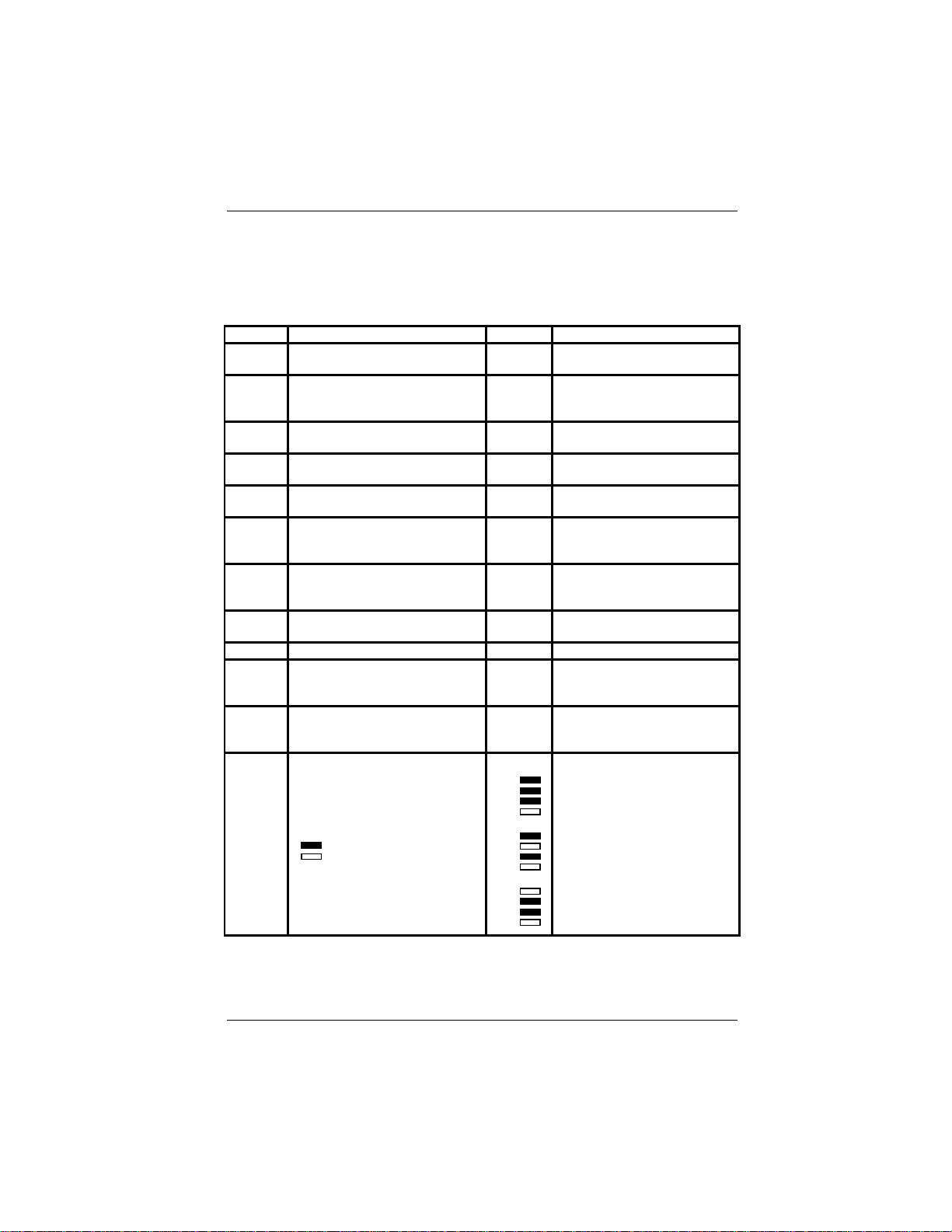
Appendix B Page 67
APPENDIX B
Configuration Jumpers
Jumper Area of Influence Link Action
J1 andJ2Bypass Links for 5 volt and 3.3 volt
CPU operation.
J3 ALE signal to IDE hard disk drive None
J4 IDE Ground Link
Connects pin 34 of P2 to ground.
J5 Serial port 1 RS485 termination None
J6 Serial port 2 RS485 termination None
J7 This link will be hard wired and is
not to be altered without first
consulting Blue Chip Technology.
J8 This link will be hard wired and is
not to be altered without first
consulting Blue Chip Technology.
J9 On-board speaker Enable None
J10 Power Save Switch Do not use
J11 Printer Interrupt selection None
J12 On-board Video Controller None
J13 CPU speed selection
A 4 by 2 row of pins exists on the
PCB. To select the required
processor frequency fit the links as
per the table.
AB, CD
EF, GH
1 - 2
None
1 - 2
1 - 2
1 - 2
None
1 - 2
2 - 3
None
1 - 2
2 - 3
1 - 2
1 - 2
2 - 3
1 - 2
2 - 3
J13
Fit ALL for 5 volt CPU,
Remove ALL for 3.3 volt CPU.
No ALE connected to IDE
interface
ALE connected to IDE interface
Pin 34 floats
Pin 34 is grounded
No termination on-board
100R & 100nF across I/P
No termination on-board
100R & 100nF across O/P
Not Allowed
Not Allowed
Factory Hard Wired
Not Allowed
Factory Hard Wired
Factory Hard Wired
On-board audio disabled
On-board audio enabled
No interrupt selected
LPT1 (IRQ 7) selected
LPT2 (IRQ 5) selected
Not Allowed
Disabled
Enabled
Processor Frequency
20MHz
= link present
= link absent
J13
25MHz
33MHz
J13
Blue Chip Technology Ltd 01270173.doc
Page 76

Page 68 Appendix B
J14 Selects either Internal or External
Battery supply.
J15 CMOS Memory clear
Either selects to power CMOS or
clears the CMOS and SRAM
J16 VESA local bus speed. None
1 - 2
2 - 3
None
1 - 2
2 - 3
1 - 2
Selects External Battery
Selects Internal Battery
Not Allowed
Battery Connected
Clears CMOS and SRAM
VESA LB operation <=33MHz
VESA LB operation >33MHz
01270173.doc Blue Chip Technology Ltd
Page 77

APPENDIX C
Connector Details
P1: Floppy (34 way header)
Pin No. Signal Pin No. Signal
1 0 Volts (Ground) 2 +RPM/Low Current
3 0 Volts (Ground) 4 Not used
5 0 Volts (Ground) 6 Not used
7 0 Volts (Ground) 8 -Index
9 0 Volts (Ground) 10 -Motor 0
11 0 Volts (Ground) 12 -Drive select 1
13 0 Volts (Ground) 14 -Drive select 0
15 0 Volts (Ground) 16 -Motor 1
17 0 Volts (Ground) 18 +Direction
19 0 Volts (Ground) 20 -Step
21 0 Volts (Ground) 22 -Write Data
23 0 Volts (Ground) 24 -Write Gate
25 0 Volts (Ground) 26 -Track 0
27 0 Volts (Ground) 28 -Write Protect
29 0 Volts (Ground) 30 -Read Data
31 0 Volts (Ground) 32 +Head Select
33 0 Volts (Ground) 34 +Disk Change
Appendix C Page 69
Blue Chip Technology Ltd 01270173.doc
Page 78

Page 70 Appendix C
P2: Hard Drive (40 way header)
Pin No. Signal Pin No. Signal
1 -Reset 2 0 Volts DC (Ground)
3 Data bit 7 (HD) 4 Data bit 8 (HD)
5 Data bit 6 (HD) 6 Data bit 9 (HD)
7 Data bit 5 (HD) 8 Data bit 10 (HD)
9 Data bit 4 (HD) 10 Data bit 11 (HD)
11 Data bit 3 (HD) 12 Data bit 12 (HD)
13 Data bit 2 (HD) 14 Data bit 13 (HD)
15 Data bit 1 (HD) 16 Data bit 14 (HD)
17 Data bit 0 (HD) 18 Data bit 15 (HD)
19 0 Volts DC (Ground) 20 Not used
21 Not used 22 0 Volts DC (Ground)
23 -IO Write (HD) 24 0 Volts DC (Ground)
25 -IO Read (HD) 26 0 Volts DC (Ground)
27 Not used 28 ALE (HD)
29 Not used 30 0 Volts DC (Ground)
31 IRQ14 32 IOCS16
33 Address 1 (HD) 34 Ground/Float (via link)
35 Address 0 (HD) 36 Address 2 (HD)
37 -Chip Select 0 (HD) 38 -Chip Select 1 (HD)
39 IDE LED Drive 40 0 Volts DC (Ground)
P3: Com 2 (10 way header)
Pin No. Signal Pin No. Signal
1 -Data Carrier Detect 2 -Data Set Ready
3 Receive Data 4 -Ready To Send
5 Transmit Data 6 -Clear To Send
7 -Data Terminal Ready 8 -Ringing Indicator
9 0 Volts (Ground) 10 Not used
01270173.doc Blue Chip Technology Ltd
Page 79

Appendix C Page 71
P4: RS422/485 Serial (10 way header)
Pin No. Signal Pin No. Signal
1 +ve Receive Data 1 2
3 -ve Receive Data 1 4 +ve Receive Data 2
5 +ve Transmit Data 1 6 -ve Receive Data 2
7 -ve Transmit Data 1 8 +ve Transmit Data 2
9
0 Volts (via 10KW)
10 -ve Transmit Data 2
+5 Volts (via 10KW)
P5: Parallel (26 way header)
Note: This pinout is different from the normal 25 way 'D' type itself.
Pin No. Signal Pin No. Signal
1 -Strobe 2 -Auto Feed XT
3 Data bit 0 4 -Error
5 Data bit 1 6 -Initialise
7 Data bit 2 8 -Select (input)
9 Data bit 3 10 0 Volts (Ground)
11 Data bit 4 12 0 Volts (Ground)
13 Data bit 5 14 0 Volts (Ground)
15 Data bit 6 16 0 Volts (Ground)
17 Data bit 7 18 0 Volts (Ground)
19 -Acknowledge 20 0 Volts (Ground)
21 Busy 22 0 Volts (Ground)
23 Paper Empty 24 0 Volts (Ground)
25 Select (Output) 26 Not Used
Blue Chip Technology Ltd 01270173.doc
Page 80
Page 72 Appendix C
P6: Feature (26 way header)
Pin No. Signal Pin No. Signal
1 0 Volts (Ground) 2 Pixel Data 0
3 0 Volts (Ground) 4 Pixel Data 1
5 0 Volts (Ground) 6 Pixel Data 2
7 Enable Video 8 Pixel Data 3
9 Enable Sync 10 Pixel Data 4
11 Enable DAC Clock 12 Pixel Data 5
13 Not Used 14 Pixel Data 6
15 0 Volts (Ground) 16 Pixel Data 7
17 0 Volts (Ground) 18 Video Clock
19 0 Volts (Ground) 20 Blanking
21 0 Volts (Ground) 22 Horizontal Sync
23 Not Used 24 Vertical Sync
25 Not Used 26 0 Volts (Ground)
P7: Video (15 way condensed D type)
Pin No. Signal Pin No. Signal
1 Analogue RED 2 Analogue GREEN
3 Analogue BLUE 4 Not Used
5 0 Volts (Ground) 6 0 Volts (Ground)
7 0 Volts (Ground) 8 0 Volts (Ground)
9 Not Used 10 0 Volts (Ground)
11 Not Used 12 Not Used
13 Horizontal Sync 14 Vertical Sync
15 Not Used
P8: Post (12 way header)
Pin No. Signal Pin No. Signal
1 AT Data bit 0 2 AT Data bit 1
3 AT Data bit 2 4 AT Data bit 3
5 AT Data bit 4 6 AT Data bit 5
7 AT Data bit 6 8 AT Data bit 7
9 POST decode 10 0 Volts (Ground)
11 +5 Volts 12
01270173.doc Blue Chip Technology Ltd
Page 81
Appendix C Page 73
P9: Mouse (6 pin mini DIN)
Pin No. Signal Pin No. Signal
1 Mouse Data 2 Not Used
3 0 Volts (Ground) 4 +5 Volts (fused)
5 Mouse Clock 6 Not Used
P10: SSD Connector (8 way header)
Pin No. Signal Pin No. Signal
1 +5 Volts 2 DEVSEL
3 +5 Volts 4 PAGESEL2
5 BUSY 6 CS_SSD
7 SMEMW/R 8 SYSRST
P11: Com 1 (9 way D)
Pin No. Signal Pin No. Signal
1 -Data Carrier Detect 2 Receive Data
3 Transmit Data 4 -Data Terminal Ready
5 0 Volts (Ground) 6 -Data Set Ready
7 -Ready To Send 8 -Clear To Send
9 -Ringing Indicator
P12: Peripheral (20 way header)
Pin No. Signal Pin No. Signal
1 Audio +ve 2 Audio -ve
3 Reset +ve 4 Reset -ve (Ground)
5 High Speed LED +ve 6 High Speed LED -ve
7 Keylock +ve 8 Keylock -ve (Ground)
9 Power LED +ve 10 Power LED -ve (Ground)
11 Turbo Switch +ve 12 Turbo Switch -ve (Ground)
13 IDE LED +ve 14 IDE LED -ve
15 +5V (fused) 16 0 Volts (Ground)
17 +3.6 Volt Battery 18 0 Volts Battery (Ground)
19 Keyboard Data 20 Keyboard Clock
Blue Chip Technology Ltd 01270173.doc
Page 82
Page 74 Appendix C
P13: Keyboard (6 pin mini DIN)
Pin No. Signal Pin No. Signal
1 Keyboard Data 2 Not Used
3 0 Volts (Ground) 4 +5 Volts (fused)
5 Keyboard Clock 6 Not Used
P14: Battery (4 way header)
Pin No. Signal
1 +3.6 Volts DC
2 Not used (key)
3 0 Volts (Ground)
4 0 Volts (Ground)
P15: Backplane Utility Connector (10 way header)
Pin No. Signal Pin No. Signal
1 Reset +ve 2 Reset -ve (Ground)
3 High Speed LED +ve 4 HS LED -ve (Ground)
5 Power LED +ve 6 Power LED -ve (Ground)
7 Keylock +ve 8 Keylock -ve (Ground)
9 Turbo Switch +ve 10 Turbo Switch -ve (Ground)
01270173.doc Blue Chip Technology Ltd
Page 83

Appendix C Page 75
P16: AT Expansion Connector
Pin No. Signal Pin No. Signal
1 -SBHE 2 -MEMCS16
3 LA23 4 -IOCS16
5 LA22 6 IRQ10
7 LA21 8 IRQ11
9 LA20 10 IRQ12
11 LA19 12 IRQ15
13 LA18 14 IRQ14
15 LA17 16 -DACK0
17 -MEMR 18 DREQ0
19 -MEMW 20 -DACK5
21 SD8 22 DREQ5
23 SD9 24 -DACK6
25 SD10 26 DREQ6
27 SD11 28 -DACK7
29 SD12 30 DREQ7
31 SD13 32 +5 Volts
33 SD14 34 -Master
35 SD15 36 0 Volts (Ground)
Blue Chip Technology Ltd 01270173.doc
Page 84

Page 76 Appendix C
P17: PC/XT Expansion Connector
Pin No. Signal Pin No. Signal
1 -IOCHCK 2 0 Volts (Ground)
3 SD7 4 Resetdrv
5 SD6 6 +5 Volts
7 SD5 8 IRQ9
9 SD4 10 -5 Volts
11 SD3 12 DREQ2
13 SD2 14 -12 Volts
15 SD1 16 -0WS
17 SD0 18 +12 Volts
19 IOCHRDY 20 0 Volts (Ground)
21 AEN 22 -SMEMW
23 SA19 24 -SMEMR
25 SA18 26 -IOW
27 SA17 28 -IOR
29 SA16 30 -DACK3
31 SA15 32 DREQ3
33 SA14 34 -DACK1
35 SA13 36 DREQ1
37 SA12 38 -REF
39 SA11 40 CLK
41 SA10 42 IRQ7
43 SA9 44 IRQ6
45 SA8 46 IRQ5
47 SA7 48 IRQ4
49 SA6 50 IRQ3
51 SA5 52 -DACK2
53 SA4 54 T/C
55 SA3 56 BALE
57 SA2 58 +5 Volts
59 SA1 60 OSC
61 SA0 62 0 Volts (Ground)
01270173.doc Blue Chip Technology Ltd
Page 85

Appendix C Page 77
ISA Bus XT Connections
A= Large gold fingers under P17 on main Component side
B= Large gold fingers under P17 on passive Component side
Pin No. Signal Pin No. Signal
A1 -IOCHCK B1 0 Volts (Ground)
A2 SD7 B2 Resetdrv
A3 SD6 B3 +5 Volts
A4 SD5 B4 IRQ9
A5 SD4 B5 -5 Volts
A6 SD3 B6 DREQ2
A7 SD2 B7 -12 Volts
A8 SD1 B8 -0WS
A9 SD0 B9 +12 Volts
A10 IOCHRDY B10 0 Volts (Ground)
A11 AEN B11 -SMEMW
A12 SA19 B12 -SMEMR
A13 SA18 B13 -IOW
A14 SA17 B14 -IOR
A15 SA16 B15 -DACK3
A16 SA15 B16 DREQ3
A17 SA14 B17 -DACK1
A18 SA13 B18 DREQ1
A19 SA12 B19 -REF
A20 SA11 B20 CLK
A21 SA10 B21 IRQ7
A22 SA9 B22 IRQ6
A23 SA8 B23 IRQ5
A24 SA7 B24 IRQ4
A25 SA6 B25 IRQ3
A26 SA5 B26 -DACK2
A27 SA4 B27 T/C
A28 SA3 B28 BALE
A29 SA2 B29 +5 Volts
A30 SA1 B30 OSC
A31 SA0 B31 0 Volts (Ground)
Blue Chip Technology Ltd 01270173.doc
Page 86

Page 78 Appendix C
ISA Bus AT Connections
C= Large gold fingers under P16 on main Component side
D= Large gold fingers under P16 on passive Component side
Pin No. Signal Pin No. Signal
C1 -SBHE D1 -MEMCS16
C2 LA23 D2 -IOCS16
C3 LA22 D3 IRQ10
C4 LA21 D4 IRQ11
C5 LA20 D5 IRQ12
C6 LA19 D6 IRQ15
C7 LA18 D7 IRQ14
C8 LA17 D8 -DACK0
C9 -MEMR D9 DREQ0
C10 -MEMW D10 -DACK5
C11 SD8 D11 DREQ5
C12 SD9 D12 -DACK6
C13 SD10 D13 DREQ6
C14 SD11 D14 -DACK7
C15 SD12 D15 DREQ7
C16 SD13 D16 +5 Volts
C17 SD14 D17 -Master
C18 SD15 D18 0 Volts (Ground)
01270173.doc Blue Chip Technology Ltd
Page 87

Appendix C Page 79
VESA Local Bus Connector
(MCA style gold edge connector)
Pin No. Signal Side A Pin No. Signal Side B
1 Data 00 1 Data 01
2 Data 02 2 Data 03
3 Data 04 3 GND
4 Data 06 4 Data 05
5 Data 08 5 Data 07
6 GND 6 Data 09
7 Data 10 7 Data 11
8 Data 12 8 Data 13
9 VCC 9 Data 15
10 Data 14 10 GND
11 Data 16 11 Data 17
12 Data 18 12 VCC
13 Data 20 13 Data 19
14 GND 14 Data 21
15 Data 22 15 Data 23
16 Data 24 16 Data 25
17 Data 26 17 GND
18 Data 28 18 Data 27
19 Data 30 19 Data 29
20 VCC 20 Data 31
21 Address 31 21 Address 30
22 GND 22 Address 28
23 Address 29 23 Address 26
24 Address 27 24 GND
25 Address 25 25 Address 24
26 Address 23 26 Address 22
27 Address 21 27 GND
28 Address 19 28 Address 20
29 GND 29 Address 18
30 Address 17 30 Address 16
31 Address 15 31 Address 14
32 VCC 32 Address 12
33 Address 13 33 Address 10
34 Address 11 34 Address 08
35 Address 09 35 GND
36 Address 07 36 Address 06
37 Address 05 37 Address 04
38 GND 38 WBACK#
39 Address 03 39 BE0#
Blue Chip Technology Ltd 01270173.doc
Page 88

Page 80 Appendix C
40 Address 02 40 VCC
41 No connection 41 BE1#
42 RESET# 42 BE2#
43 D/C# 43 GND
44 M/IO# 44 BE3#
45 W/R# 45 ADS#
46 RDYRTN# 46 LRDY#
47 GND 47 LDEV#
48 IRQ9 48 LREQ#
49 BRDY# 49 GND
50 BLAST# 50 LGNT#
51 ID0 51 VCC
52 ID1 52 ID2
53 GND 53 ID3
54 LCLK 54 ID4
55 VCC 55 LKEN#
56 LBS16# 56 LEADS#
01270173.doc Blue Chip Technology Ltd
Page 89

Appendix D Page 81
APPENDIX D
CMOS RAM Map
A map of CMOS RAM as configured by the AMIBIOS for the Blue Chip
Technology DX1 SBC is shown in the following table.
Description
00h - 0Fh Standard IBM AT compatible RTC and Status Register data definitions.
10h Floppy Drive Type
Bits 7-4 Drive A: Type
0 No Drive
1 360 KB Drive
2 1.2 MB Drive
3 720 KB Drive
4 1.44 MB Drive
5 2.88 MB Drive
Bits 3-0 Drive B: Type (bit settings same as A)
11h Bit 7 Mouse Support Option (1 = Enabled)
Bit 6 Above 1 MB Memory Test (1 = Enabled)
Bit 5 Memory Test Tick Sound (1 = Enabled)
Bit 4 Memory Parity Error Check (1 = Enabled)
Bit 3 Hit <DEL> Message Display (1 = Enabled)
Bit 2 Hard Disk Type 47 RAM Area (1 = 0:300h)
Bit 1 Wait for <F1> if Any Error (1 = Enabled)
Bit 0 System Boot Up Num Lock (1 = Enabled)
12h Hard Disk Data
Bits 7-4 Hard Disk Drive C: Type
0 No drive
1-14 Hard drive Type 1-14
16 Hard Disk Type 16-255 (actual Hard Drive Type is in CMOS RAM 1Ah)
Bits 3-0 Hard Disk Drive D: Type (Same as C:)
Blue Chip Technology Ltd 01270173.doc
Page 90
Page 82 Appendix D
13h Bit 7 Typematic Rate Programming(1 = Enabled)
Bits 6-5 Typematic Rate Delay (in milliseconds)
00 250 ms 01 500 ms
10 750 ms 11 100 ms
Bits 4-2 Typematic Rate (in characters per second)
000 6 cps 001 8 cps
010 10 cps 011 12 cps
100 15 cps 101 20 cps
110 24 cps 111 30 cps
14h Equipment Byte
Bits 7-6 Number of Floppy Drives
00b 1 Drive
01b 2 Drives
10b-11b Reserved
Bits 5-4 Monitor Type
00b Not CGA or MDA
01b 40x25 CGA
10b 80x25 CGA
11b MDA (Monochrome)
Bit 3 Display Enabled (1 = Enabled)
Bit 2 Keyboard Enabled (1 = Enabled)
Bit 1 Math coprocessor Installed (1 = Enabled)
Bit 0 Floppy Drive Installed (0 = On)
15h Base Memory (in 1 KB increments), Low Byte
16h Base Memory (in 1 KB increments), High Byte
17h Extended Memory (in 1 KB increments), Low Byte
18h Extended Memory (in 1 KB increments), High Byte (Max 15 MB)
19h Hard Disk C: Drive Type
0-15 Reserved
16-255 Hard Drive Type 16-255
1Ah Hard Disk D: Drive Type (Same as Drive C: above)
1Bh User-Defined Drive C: - # of Cylinders, Low Byte
1Ch User-Defined Drive C: - # of Cylinders, High Byte
1Dh User-Defined Drive C: - Number of Heads
1Eh User-Defined Drive C: - Write Precompensation Cylinder, Low Byte
1Fh User-Defined Drive C: - Write Precompensation Cylinder, High Byte
20h User-Defined Drive C: - Control Byte (80h if # of heads is equal or greater than 8)
21h User-Defined Drive C: - Landing Zone, Low Byte
22h User-Defined Drive C: - Landing Zone, High Byte
01270173.doc Blue Chip Technology Ltd
Page 91

Appendix D Page 83
23h User-Defined Drive C: - # of Sectors
24h User-Defined Drive D: - # of Cylinders, Low Byte
25h User-Defined Drive D: - # of Cylinders, High Byte
26h User-Defined Drive D: - Number of Heads
27h User-Defined Drive D: - Write Precompensation Cylinder, Low Byte
28h User-Defined Drive D: - Write Precompensation Cylinder, High Byte
29h User-Defined Drive D: - Control Byte (80h if # of heads is equal or greater than 8)
2Ah User-Defined Drive D: - Landing Zone, Low Byte
2Bh User-Defined Drive D: - Landing Zone, High Byte
2Ch User-Defined Drive D: - # of Sectors
2Dh Configuration Options
Bit 7 Weitek Processor (1 = Present)
Bit 6 Floppy Drive Seek At Boot (1 = Enabled)
Bit 5 System Boot Up Sequence (1 = A:, C:)
Bit 4 System Boot Up CPU Speed (1 = High)
Bit 3 External Cache Memory (1 = Enabled)
Bit 2 Internal Cache Memory (1 = Enabled)
Bit 1 Fast Gate A20 Option (1 = Enabled)
Bit 0 Turbo Switch Function (1 = Enabled)
2Eh Standard CMOS Checksum, High Byte
2Fh Standard CMOS Checksum, Low Byte
30h Extended Memory, Low Byte
31h Extended Memory, High Byte (Maximum 15 MB)
32h Century Byte (BCD value for the century)
33h Information Flag
Bit 7 BIOS Size (1 = 128 KB)
Bits 6-0 Reserved
34h Bit 7 Boot Sector Virus Protection (1 = Enabled)
Bit 6 Password:
0 Always
1 Setup
Bit 5 Adaptor ROM Shadow C800,16K (1 = Enabled)
Bit 4 Adaptor ROM Shadow CC00,16K (1 = Enabled)
Bit 3 Adaptor ROM Shadow D000,16K (1 = Enabled)
Bit 2 Adaptor ROM Shadow D400,16K (1 = Enabled)
Bit 1 Adaptor ROM Shadow D800,16K (1 = Enabled)
Bit 0 Adaptor ROM Shadow DC00,16K (1 = Enabled)
Blue Chip Technology Ltd 01270173.doc
Page 92

Page 84 Appendix D
35h Bit 7 Adaptor ROM Shadow E000,16K (1 = Enabled)
Bit 6 Adaptor ROM Shadow E400,16K (1 = Enabled)
Bit 5 Adaptor ROM Shadow E800,16K (1 = Enabled)
Bit 4 Adaptor ROM Shadow EC00,16K (1 = Enabled)
Bit 3 System BIOS Shadow F000,64K (1 = Enabled)
Bit 2 Video ROM Shadow C000, 16K (1 = Enabled)
Bit 1 Video ROM Shadow C400,16K (1 = Enabled)
Bit 0 Numeric Processor Test (1 = Enabled)
36h Bit 7 IDE Block Mode Transfer
0 Disabled
1 Enabled
Bits 6-5 CPU Internal Clock Mode
00 2X 01 1X
Bit 4 IDE Standby Mode
0 Disabled
1 Enabled
Bits 3-0 Auto KeyLock Timeout
0000 Disabled 0001 1 Min.
0010 2 Min. 0011 3 Min.
0100 4 Min. 0101 5 Min.
0110 6 Min. 0111 7 Min.
1000 8 Min. 1001 9 Min.
1010 10 Min. 1011 11 Min.
1100 12 Min. 1101 13 Min
1110 14 Min. 1111 15 Min.
37h Reserved
38h - 3Dh Encrypted Password
3Eh Extended CMOS Checksum, High Byte (includes 34h - 3Dh)
3Fh Extended CMOS Checksum, Low Byte (includes 34h - 3Dh)
40h Reserved
01270173.doc Blue Chip Technology Ltd
Page 93

Appendix D Page 85
41h Bit 7-6 Cache Read Option
01 3-2-2-2 10 3-1-1-1
11 2-1-1-1
Bits 5-4 Cache Write Option
01 2 W.S. 10 1 W.S.
11 0 W.S.
Bit 3 Refresh Cycle
0 Slow
1 Fast
Bit 2 DRAM Type
0 PageMode
1 FastPage
Bits 1-0 DRAM Wait State(s)
01 2 W.S 10 1 W.S
11 0 W.S.
42h Bit 7 Non-Cacheable Block-2 Enable
0 Disabled
1 Enabled
Bit 6 Non-Cacheable Block-1 Enable
0 Disabled
1 Enabled
43h Bit 6 CoProcessor Ready
0 Delay 1T
1 No Delay
Bit 5 Check ELBA# Signal
0 in T1
1 in T2
44h Bits 3-0 Non-Cacheable Block-1 Base
45h Reserved
46h Bits 7-0 Non-Cacheable Block-1 Size
47h Reserved
48h Bits 5-4 Non-Cacheable Block-2 Base
49h Reserved
4Ah Bits 7-0 Non-Cacheable Block-2 Size
4Bh Bit 7 Memory Remapping
0 Disabled
1 Enabled
Blue Chip Technology Ltd 01270173.doc
Page 94

Page 86 Appendix D
4Ch Bits 7-6 F Segment Shadow RAM
00 Disabled 01 Enabled
10 Cached 11 Into-486
Bits 5-4 E Segment Shadow RAM
00 Disabled 01 Enabled
10 Cached 11 Into-486
4Dh Bits 7-6 C000-C3FF Shadow RAM
00 Disabled 01 Enabled
10 Cached 11 Into-486
Bits 5-4 C400-C7FF Shadow RAM
00 Disabled 01 Enabled
10 Cached 11 Into-486
Bits 3-2 C800-CBFF Shadow RAM
00 Disabled 01 Enabled
10 Cached 11 Into-486
Bits 1-0 CC00-CFFF Shadow RAM
00 Disabled 01 Enabled
10 Cached 11 Into-486
4Eh Bits 7-6 D000-D3FF Shadow RAM
00 Disabled 01 Enabled
10 Cached 11 Into-486
Bits 5-4 D400-D7FF Shadow RAM
00 Disabled 01 Enabled
10 Cached 11 Into-486
Bits 3-2 D800-DBFF Shadow RAM
00 Disabled 01 Enabled
10 Cached 11 Into-486
Bits 1-0 DC00-DFFF Shadow RAM
00 Disabled 01 Enabled
10 Cached 11 Into-486
4Fh Reserved
50h Bit 6 Hold PD Bus
0 1~2 T
1 2~3 T
Bits 5-0 Refresh Divider
000000 64 000001 1
000010 2 000011 4
000100 8 000101 16
000110 32
01270173.doc Blue Chip Technology Ltd
Page 95

51h Bits 5-3 Keyboard Clock Select
000 CPUCLK/6 001 CPUCLK/5
010 CPUCLK/4 011 CPUCLK/3
100 CPUCLK/2 110 9.5 MHz
111 7.2 MHz
Bits 2-0 AT Clock Select
000 CPUCLK/6 001 CPUCLK/5
010 CPUCLK/4 011 CPUCLK/3
100 CPUCLK/2 110 7.2 MHz
111 CPUCLK/8
52h Bit 7 Data Location of Local Bus
0 ISA Bus
1 PD Bus
Bits 6-5 LOWA20#, RC Emulation
00 None 01 GA20
10 Both
Bit 4 Stretch 0WS# Signal Option
0 Do Not
1 ½ ATCLK
Bits 3-0 IO Recovery Time of ISA/PCB
0000 0/0 BCLK 0001 1/1 BCLK
0010 2/2 BCLK 0011 3/3 BCLK
0100 5/3 BCLK 0101 7/3 BCLK
0110 9/3 BCLK 0111 12/3 BCLK
1100 5/5 BCLK 1101 7/7 BCLK
1110 9/9 BCLK 1111 12/12BCLK
53h Reserved
54h Bit 6 AUTO Config Function
0 Disabled
1 Enabled
Bit 5 Hardware Parity Check
0 Disabled
1 Enabled
55h - 5Fh Reserved
60h Bits 7-0 Device-1 Timeout
61h Bits 7-0 Device-2 Timeout
62h Bits 7-0 Device-3 Timeout
63h Bits 7-0 Device-4 Timeout
64h Bits 7-0 Device-5 Timeout
Appendix D Page 87
Blue Chip Technology Ltd 01270173.doc
Page 96

Page 88 Appendix D
65h -7Fh Reserved
01270173.doc Blue Chip Technology Ltd
Page 97

Appendix E Page 89
APPENDIX E
Chipset Registers
The AMIBIOS for the Blue Chp Technology DX1 SBC sets the following values
in the chipset registers.
Offset Description
54h Bit 6 AUTO Config Function
0 Disabled
1 Enabled
Bit 5 Hardware Parity Check
0 Disabled
1 Enabled
C1h Bit 7-6 Cache Read Option
01 3-2-2-2 10 3-1-1-1
11 2-1-1-1
Bits 5-4 Cache Write Option
01 2 W.S. 10 1 W.S.
11 0 W.S.
Bit 3 Refresh Cycle
0 Slow
1 Fast
Bit 2 DRAM Type
0 PageMode
1 FastPage
Bits 1-0 DRAM Wait State(s)
01 2 W.S 10 1 W.S
11 0 W.S.
C2h Bit 7 Non-Cacheable Block-2 Enable
0 Disabled
1 Enabled
Bit 6 Non-Cacheable Block-1 Enable
0 Disabled
1 Enabled
Blue Chip Technology Ltd 01270173.doc
Page 98

Page 90 Appendix E
C3h Bit 6 CoProcessor Ready
0 Delay 1T
1 No Delay
Bit 5 Check ELBA# Signal
0 in T1
1 in T2
C4h Bits 3-0 Non-Cacheable Block-1 Base
C5h Reserved
C6h Bits 7-0 Non-Cacheable Block-1 Size
C7h Reserved
C8h Bits 5-4 Non-Cacheable Block-2 Base
C9h Reserved
CAh Bits 7-0 Non-Cacheable Block-2 Size
CBh Bit 7 Memory Remapping
0 Disabled
1 Enabled
CCh Bits 7-6 F Segment Shadow RAM
00 Disabled 01 Enabled
10 Cached 11 Into-486
Bits 5-4 E Segment Shadow RAM
00 Disabled 01 Enabled
10 Cached 11 Into-486
CDh Bits 7-6 C000-C3FF Shadow RAM
00 Disabled 01 Enabled
10 Cached 11 Into-486
Bits 5-4 C400-C7FF Shadow RAM
00 Disabled 01 Enabled
10 Cached 11 Into-486
Bits 3-2 C800-CBFF Shadow RAM
00 Disabled 01 Enabled
10 Cached 11 Into-486
Bits 1-0 CC00-CFFF Shadow RAM
00 Disabled 01 Enabled
10 Cached 11 Into-486
01270173.doc Blue Chip Technology Ltd
Page 99

Appendix E Page 91
CEh Bits 7-6 D000-D3FF Shadow RAM
00 Disabled 01 Enabled
10 Cached 11 Into-486
Bits 5-4 D400-D7FF Shadow RAM
00 Disabled 01 Enabled
10 Cached 11 Into-486
Bits 3-2 D800-DBFF Shadow RAM
00 Disabled 01 Enabled
10 Cached 11 Into-486
Bits 1-0 DC00-DFFF Shadow RAM
00 Disabled 01 Enabled
10 Cached 11 Into-486
CFh Reserved
D0h Bit 6 Hold PD Bus
0 1~2 T
1 2~3 T
Bits 5-0 Refresh Divider
000000 64 000001 1
000010 2 000011 4
000100 8 000101 16
000110 32
D1h Bits 5-3 Keyboard Clock Select
000 CPUCLK/6 001 CPUCLK/5
010 CPUCLK/4 011 CPUCLK/3
100 CPUCLK/2 110 9.5 MHz
111 7.2 MHz
Bits 2-0 AT Clock Select
000 CPUCLK/6 001 CPUCLK/5
010 CPUCLK/4 011 CPUCLK/3
100 CPUCLK/2 110 7.2 MHz
111 CPUCLK/8
Blue Chip Technology Ltd 01270173.doc
Page 100

Page 92 Appendix E
D2h Bit 7 Data Location of Local Bus
0 ISA Bus
1 PD Bus
Bits 6-5 LOWA20#, RC Emulation
00 None 01 GA20
10 Both
Bit 4 Stretch 0WS# Signal Option
0 Do Not
1 ½ ATCLK
Bits 3-0 IO Recovery Time of ISA/PCB
0000 0/0 BCLK 0001 1/1 BCLK
0010 2/2 BCLK 0011 3/3 BCLK
0100 5/3 BCLK 0101 7/3 BCLK
0110 9/3 BCLK 0111 12/3 BCLK
1100 5/5 BCLK 1101 7/7 BCLK
1110 9/9 BCLK 1111 12/12BCLK
D3h Reserved
E0h Bits 7-0 Device-1 Timeout
E1h Bits 7-0 Device-2 Timeout
E2h Bits 7-0 Device-3 Timeout
E3h Bits 7-0 Device-4 Timeout
E4h Bits 7-0 Device-5 Timeout
01270173.doc Blue Chip Technology Ltd
 Loading...