

Page 1

BCT-ETX-C3-XXX
ETX format Single Board PC
User Manual
Document Reference BCTETXC3 Manual
Document Issue Level 1.3
Manual covers PCBs with the following Issue 1.x (where 'x' is any alphanumeric).
Blue Chip Technology Ltd.
Chowley Oak
Tattenhall
Chester
CH3 9EX
U.K.
Telephone: +44 (0)1829 772000
Facsimile: +44 (0)1829 772001
www.bluechiptechnology.co.uk
Page 2

BCT-ETX-C3-XXX SINGLE BOARD COMPUTER
Contents
BLUE CHIP TECHNOLOGY LTD. .............................................................................. 1
INTRODUCTION ......................................................................................................... 4
COMPANY PROFILE .......................................................................................................................... 4
COPYRIGHT ....................................................................................................................................... 4
LIMITATIONS OF LIABILITY .............................................................................................................. 4
RELATED PUBLICATIONS ................................................................................................................ 5
TRADEMARKS.................................................................................................................................... 5
PRECAUTIONS................................................................................................................................... 6
Electro-Static Discharges ............................................................................................................................. 6
On-Board Battery ......................................................................................................................................... 6
BIOS & CMOS RAM..................................................................................................................................... 6
Electromagnetic Compatibility ..................................................................................................................... 6
WARNING ................................................................................................................... 7
USER GUIDE .............................................................................................................. 8
MANUAL ORGANISATION ................................................................................................................. 8
OVERVIEW ......................................................................................................................................... 9
BCT-ETX-C3-XXX PROCESSOR BOARD PHOTO .........................................................................10
5-VOLT POWER ....................................................................................................... 14
5-VOLT STAND–BY POWER .................................................................................... 14
BOARD LAYOUT ..............................................................................................................................15
Top Surface of the PCB .............................................................................................................................. 15
INSTALLATION ......................................................................................................... 16
MOUNTING .......................................................................................................................................16
THERMAL PLATE .............................................................................................................................17
CONNECTOR PIN ASSIGNMENT ...................................................................................................18
COOLING ..........................................................................................................................................32
CABLING ...........................................................................................................................................32
EMC ISSUES ....................................................................................................................................33
INTERRUPT ASSIGNMENT TABLE.................................................................................................34
DIRECT MEMORY ACCESS CHANNELS (DMA) ............................................................................35
I/O ADDRESS MAP (HEX) ................................................................................................................35
MEMORY ADDRESS MAP (HEX) ....................................................................................................36
PERIPHERAL COMPONENT INTERCONNECT DEVICES (PCI) ...................................................36
USING THE BOARD ................................................................................................. 37
Page 3

BCT-ETX-C3-XXX SINGLE BOARD COMPUTER
BIOS SETTINGS ...............................................................................................................................37
LOADING OPERATING SYSTEMS & DRIVERS .............................................................................37
PROGRAMMING THE BOARD ........................................................................................................38
PROGRAMMING THE BOARD ........................................................................................................38
User EEPROM ............................................................................................................................................ 38
Watchdog facility ................................................................ ................................ ........................................ 38
Accessing Software 'INT 50h' Functions..................................................................................................... 39
MAINTENANCE ................................................................................................................................40
TROUBLESHOOTING GUIDE .................................................................................. 41
AMENDMENT HISTORY........................................................................................... 42
Page 4

BCT-ETX-C3-XXX SINGLE BOARD COMPUTER INTRODUCTION
INTRODUCTION
COMPANY PROFILE
Blue Chip Technology is a leading specialist PC product manufacturer in Europe, providing innovation with
quality design and manufacturing from a single source.
Based in the North West of England, our purpose built complex contains both advanced research and
development facilities, and manufacturing facilities.
Specialising in the provision of industrial computing and electronic solutions for a wide range of UK and
European organisations, Blue Chip Technology has one of the UK's largest portfolios of industrial PCs, Single
Board Computers, peripherals and data acquisition cards. This extensive range of products, coupled with our
experience and expertise, enables Blue Chip Technology to offer an industrial processing solution for any
application. This is one of the products from our portfolio, providing you with a cost effective product
development and volume production tool.
A unique customisation and specialised system integration service is also available, delivering innovative
solutions to customers problems. The company's success and reputation in this area has led to a number of
large design and manufacturing projects for major companies.
British Standards Institute approval (BS EN 9001) means that all of Blue Chip Technology's design and
manufacturing procedures are strictly controlled, ensuring the highest levels of quality, reliability and
performance.
Blue Chip Technology are committed to the single European market, and continue to invest in the latest
technology and skills to provide high performance computer and electronic solutions for a world-wide
customer base.
COPYRIGHT
All rights reserved. No part of this publication may be reproduced, stored in any retrieval system, or
transmitted, in any form or by any means, electronic, mechanical, photocopied, recorded or otherwise, without
the prior permission, in writing, from the publisher. For permission in the UK please contact Blue Chip
Technology.
Information offered in this manual is believed to be correct at the time of printing. Blue Chip Technology
accepts no responsibility for any inaccuracies. The information contained herein is subject to change without
notice. There are no express or implied licences granted herein to any intellectual property rights of Blue Chip
Technology Ltd.
LIMITATIONS OF LIABILITY
In no event shall Blue Chip Technology be held liable for any loss, expenses or damages of any kind
whatsoever, whether direct, indirect, incidental or consequential, arising from the design or use of this product
or the support materials supplied with this product. If this product proves to be defective, Blue Chip
Technology is only obliged to replace or refund the purchase price at Blue Chip Technology's discretion
according to their Terms and Conditions of Sale.
Page 5

BCT-ETX-C3-XXX SINGLE BOARD COMPUTER INTRODUCTION
RELATED PUBLICATIONS
The following publications will provide useful information related to the Standard Personal Computer and can
be used in conjunction with this manual.
IBM Personal Computer AT Technical Reference, 1502494, IBM, 1984.
IBM Personal System/2 and Personal Computer BIOS Interface Technical Reference, 15F0306, IBM,
1987.
The Programmers PC Sourcebook, Microsoft
The Winn L. Rosch Hardware Bible, Brady
TRADEMARKS
All trademarks and registered names acknowledged.
IBM, PC, AT and PS/2 are trademarks of International Business Machines Corporation (IBM).
Phoenix BIOS is a trademark of Phoenix Technologies Inc
Intel is a registered trademark of the Intel Corporation.
All 80x86 and Pentium processors are registered trademarks of Intel Corporation.
MS-DOS and WINDOWS are registered trademarks of the Microsoft Corporation.
Linux is a registered trademark of Linus Torvalds.
ATA-Disk Chip is a trademark of Silicon Storage Technology Inc.
Page 6

BCT-ETX-C3-XXX SINGLE BOARD COMPUTER INTRODUCTION
PRECAUTIONS
Certain precautions are necessary when designing with, handling, and using circuit boards. It is imperative
that precautions are taken at all stages to avoid electro-static discharges, which will damage boards. Those
boards fitted with an on-board lithium battery must be handled carefully to avoid maltreatment of the
battery that could create a hazard.
ELECTRO-STATIC DISCHARGES
The devices on this card can be totally destroyed by static electricity. Also bear in mind that the damage
caused by static electricity may be partial and not immediately obvious. This could have an effect on your
product's reliability and warranty. Ensure that you take necessary static precautions, ideally you should
wear an approved wrist strap or if that is not possible, touch a suitable ground to discharge any static build
up. This should be repeated if the handling is for any length of time.
When carrying the board around, please place it into the anti-static bag in which it came. This will prevent
any static electricity build up. Do not use black anti-static bags because these tend to be conductive and will
discharge any on-board battery.
ON-BOARD BATTERY
The BCT-ETX-C3-XXX board does not have an on-board lithium cell connected, however the base board to
which it connects may be equipped with a cell. To that end the following precautions apply and should be
observed. If the battery is mistreated in any way there is a very real possibility of fire, explosion, and harm.
Great care should be taken with this type of battery. Under NO circumstances should it be:
short-circuited
exposed to temperatures in excess of 100 ºC or burnt
immersed in water
unsoldered
recharged
disassembled
Expired batteries remain hazardous and must be disposed of in a safe manner.
BIOS & CMOS RAM
Please be aware that on single board computer products, it is possible to create configurations within the
CMOS RAM that make booting impossible. If this should happen, clear the CMOS settings, (see the
description of the Jumper Settings on the base board being used for details).
ELECTROMAGNETIC COMPATIBILITY
This product meets the requirements of the European EMC Directive (89/336/EEC) and is eligible to bear
the CE mark.
It has been assessed operating in a Blue Chip Technology housing. However, because the board can be
installed in a wide variety of base boards and chassis, certain conditions have to be applied to ensure that the
compatibility is maintained. Subject to those conditions, it meets the requirements for an industrial
environment (ITE Class A product).
Page 7
BCT-ETX-C3-XXX SINGLE BOARD COMPUTER INTRODUCTION
The board must be installed in a computer system chassis that provides screening suitable for an
industrial environment.
Any recommendations made by the computer system manufacturer/supplier must be complied with
regarding earthing and the installation of boards.
Any metal back plate must be securely screwed to the chassis of the computer to ensure good metal-to-
metal (i.e. earth) contact.
Connector bodies must be securely connected to the enclosure.
The external cabling to boards causes most EMC problems. It is imperative that any external cabling to
the board is totally screened, and that the screen of the cable connects to the metal end bracket of the
board or the enclosure and hence to earth. It is recommended that round, screened cables with a braided
wire screen are used in preference to those with a foil screen and drain wire. Use metal connector shells
that connect around the full circumference of the cable screen: they are far superior to those that earth
the screen by a simple “pig-tail”.
The keyboard and mouse will play an important part in the compatibility of the processor card since they
are ports into the board. Similarly, they will affect the compatibility of the complete system. Fully
compatible peripherals must be used otherwise the complete system could be degraded. They may
radiate or behave as if keys/buttons are pressed when subject to interference. Under these circumstances
it may be beneficial to add a ferrite clamp on the leads as close as possible to the connector. A suitable
type is the Chomerics type H8FE-1004-AS.
USB cables should be high quality screened types.
Ensure that the screens of any external cables are bonded to a good RF earth at the remote end of the
cable.
Failure to observe these recommendations may invalidate the EMC compliance.
Warning
This is a Class A product. In a domestic environment this product may cause radio
interference in which case the user may be required to take adequate measures.
Page 8

BCT-ETX-C3-XXX SINGLE BOARD COMPUTER USER GUIDE
USER GUIDE
MANUAL ORGANISATION
This manual describes in detail the Blue Chip Technology BCT-ETX-C3-XXX Single Board processor card.
We have tried to include as much information as possible but we have not duplicated information that is
provided in the standard IBM Technical References, unless it proved to be necessary to aid in the
understanding of the BCT-ETX-C3-XXX.
The manual is sectioned as follows:
Overview, listing the board's features and specification;
Layout, showing where the various items are located;
Installation, and associated issues;
Using the board, including the peripherals;
Troubleshooting guide;
Connector Pin-Out details.
We strongly recommend that you study this manual carefully before attempting to interface with BCT-ETXC3-XXX or change the standard configurations. Whilst all the necessary information is available in this
manual we would recommend that unless you are confident, you contact your supplier for guidance. IT IS
PARTICULARLY IMPORTANT THAT YOU READ THE SECTION 'PRECAUTIONS' BEFORE
HANDLING THE BOARD.
If you have any suggestions or find any errors concerning this manual and want to inform us of these, please
contact our Technical Services department with the relevant details.
Page 9

BCT-ETX-C3-XXX SINGLE BOARD COMPUTER USER GUIDE
OVERVIEW
1.1 Introduction
The Blue Chip Technology BCT-ETX-C3-XXX Single Board PC integrates the latest advances in low
power processor, memory, and I/O technologies to provide an ideal platform for embedded applications. The
BCT-ETX-C3-XXX complies with the embedded ETX standard set of Bus interface signals and peripheral IO
devices interfaces on a single card. The concept of ETX is to provide the user with a standard connector
interface with fixed connector locations and predefined IO functions. This allows the user to concentrate their
design efforts on the supporting base board for the target application. This modular approach provides a cost
effective means of system upgrade and allows the user to easily validate a number of CPU board
price/power/performance options.
The board is available with CPU build options of an extremely Low Power VIA Eden ESP 400 (400MHz) and
Low Power VIA C3 1Gz processor. On-board voltage regulator circuits provide the required voltages for the
processor from the incoming 5 volt power supply. The 400MHz ESP C3 version of BCT-ETX-C3-XXX is
targeted at lower cost, power conscious, performance driven applications. The 1Ghz C3 build offers a higher
performance solution for applications where reduced power is less of a requirement. In addition a special
266MHz version is available for the lowest power consumption applications. Further variants are VIA Eden
733Mhz and VIA C3 800Mhz processors.
The processor maintains full backward compatibility with the 8086, 80286, i386 and Intel486 processors.
It supports both read and write burst mode bus cycles, and includes separate on-chip code and data caches
which employ a write-back policy. Cache is integrated within the CPU and operates at the full CPU frequency
giving excellent performance. Cache size is 128K L1 and 64K L2. Also integrated into the processor is an
advanced numeric co-processor which significantly increases the speed of floating point operations, whilst
maintaining backward compatibility with Intel486 math co-processor and complying with ANSI/IEEE
standard 754-1985.
The memory interface supports up to 512MB of 3.3V PC133 SDRAM, in a standard 144 pin SODIMM
socket.
Solid State expansion is available through an ATA Disk Chip option, providing up to 512MB. This option can
be populated at the Factory or by the user.
The BCT-ETX-C3-XXX utilises VIA’s PN133T chipset to integrate many peripherals. These include: VGA
controller with CRT, LVDS and LCD interfaces, ATA-100 IDE interface, ATA solid state disk, 10/100 Fast
Ethernet controller, floppy disk interface, quad USB ports, dual serial ports, parallel port, real-time clock,
keyboard and mouse (PS/2) controller, AC’97 audio interface. Connection to these functions is made through
a standard set of ETX connectors onto a base board. The base board can then bring these signals to either
Industry standard or customer specified connectors. The base board may be a custom design, developed for a
specific application or a standard solution offered by Blue Chip Technology.
The BCT-ETX-C3-XXX will drive up to four external PCI cards, all of which can perform Bus Mastering.
Further IO expansion is available through the 16-bit ISA bus.
A full set of software drivers and utilities are available to allow advanced operating systems such as
Windows™ 9x, Me, NT, 2000 & XP to take full advantage of all the hardware capabilities.
Page 10
BCT-ETX-C3-XXX SINGLE BOARD COMPUTER USER GUIDE
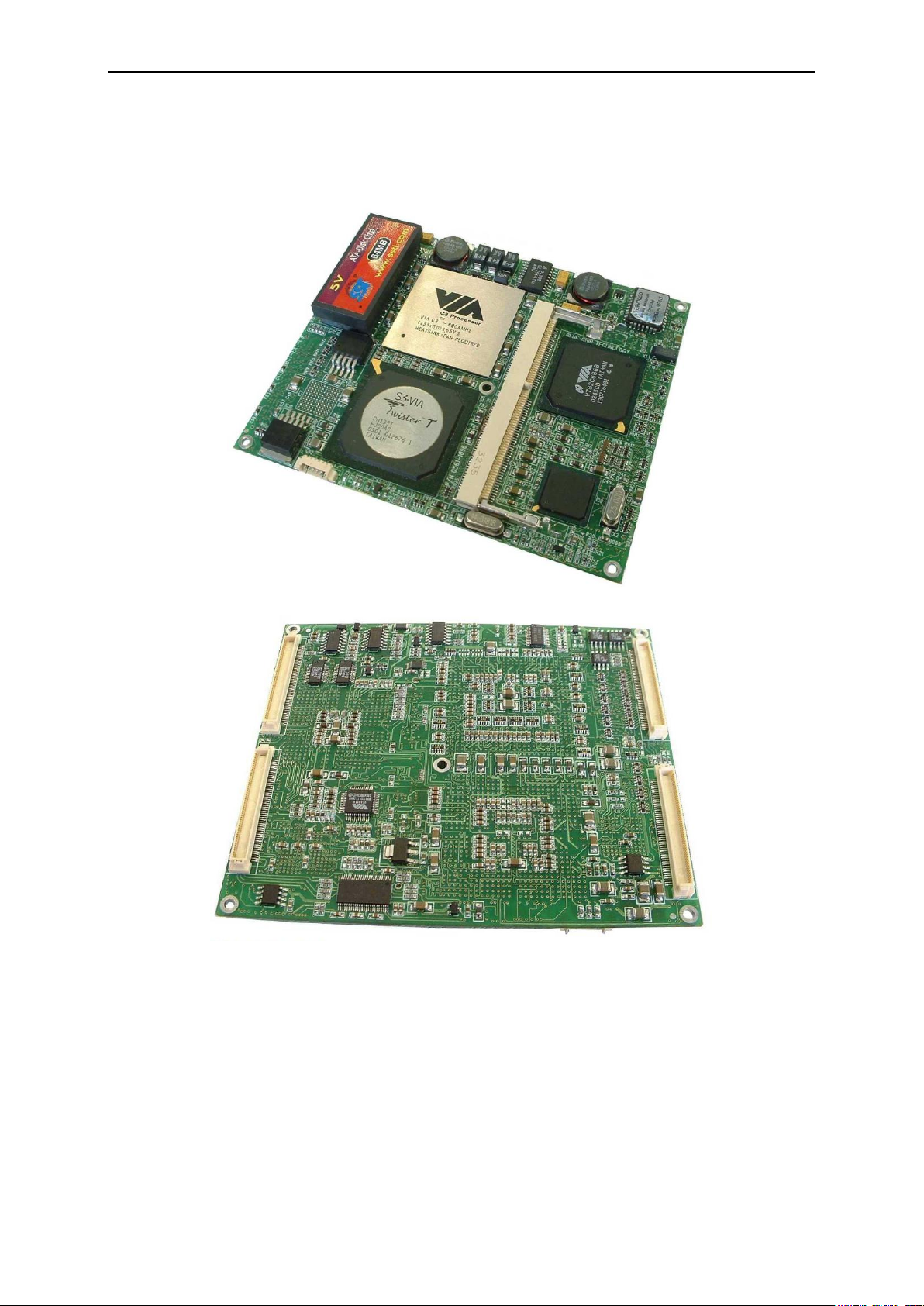
BCT-ETX-C3-XXX PROCESSOR BOARD PHOTO
Page 11

BCT-ETX-C3-XXX SINGLE BOARD COMPUTER USER GUIDE
Board Level Features
CPU: VIA C3 800MHz/1Ghz (128KB L1 & 64KB L2 cache)
VIA Eden 266/400/733MHz (128KB L1 & 64KB L2 cache)
CPU Cooling: Passive CPU heat spreader/ heat sink cooling for lower
performance parts
Chipset: VIA PN133T Chipset including:
VT8606 North Bridge.
VT82C686B South Bridge.
BIOS: Phoenix BIOS, with Ethernet Boot ROM option, BCT BIOS
extensions and INT calls
Support for APM and VIA Power Saver (Long-Haul) technology.
Customer Splash screen option available
Memory:
64MB to 512Mbyte PC133/100/66 SDRAM expansion using
horizontal 144 pin SODIMM.
3V3 only operation.
SPD scheme for SDRAM identification.
No Support for parity memory.
Cache: 128KB L1 and 64KB L2 Cache is integrated into the CPU
Solid State Disk:
ADC (ATA Flash) site for onboard Flash optional. Note height when
fitted.
Onboard Peripherals:
Graphics:
Integrated AGP (x4) Graphics controller based on S3 Savage 4
CRT SVGA at 1600 x 1200 resolution.
Direct LCD support for STN, DSTN and TFT up to 18 bit
Dual channel LVDS for up to 18 bit panels
Selection between Direct LCD and LVDS is a build option.
8 to 32Mbyte of video memory (Shared Memory Architecture SMA)
Supports 848*480 & 1024*512 widescreen resolutions
Ethernet:
10/100 Base-T Ethernet using Intel 82551ER
Boot ROM option within the BIOS set-up for remote booting (PXE).
Note: the base board must carry the magnetic for network isolation
Storage:
ATA100/66/33 EIDE HDD (quad drives, dual connectors) provided by
South Bridge. 80 way cable detection incorporated.
Page 12

BCT-ETX-C3-XXX SINGLE BOARD COMPUTER USER GUIDE
512 bytes of E²PROM with Device Drivers.
Audio:
Integrated Soundblaster/Direct sound AC97 controller
Line In/Out, Microphone and CD in.
Note: CD in and Line in share the same pins and are therefore
mutually exclusive.
Monitoring:
CPU Core(1.05 to 1.6V), North Bridge Core(2.5), 3V3 and 5V voltage
monitors
Two on board thermistors for system thermal monitoring
Hardware Watchdog timer with configurable timeout.
Software enabled/disable through an IO port. The time-out results in a
system Reset. Device Driver support is available.
Power monitoring of the +5 volt rail included in the Reset circuit. Reset
generated if the rail falls below 4.65 volts.
Communications:
Quad USB Ver 1.x Compliant
Two 16C550 compatible serial ports at TTL level signalling.
Note: Base board must provide RS232 or RS485 transceivers.
One IR port. This is shared with the second serial port UART.
Parallel port with Bi-directional, EPP & ECP.
Floppy interface with support for dual 1.44MB FDD
Note: the floppy or parallel port are an option that is determined at
boot time by strapping a pin on the base board ie if floppy port
selected then there is no parallel port and vice-versa)
PS/2 compatible keyboard and mouse port. Connector located on
baseboard
Miscellaneous:
PC standard Real Time Clock is integrated into the South Bridge. Due
to height constraints, the battery has to be located on the host board.
Speaker, Reset switch, Power Switch, Hard Disk Activity LED,
Suspend Switch and external Lithium coin cell are all supported and
located on the base board.
Expansion Bus:
As per ETX specification, 4 connectors (X1-X4)
The host board supports four standard 5V 32 bit 33MHz PCI slots. The
PCI is V2.2 compliant.
ISA Expansion supports three standard 16-bit ISA slots.
Connector X1 provides the PCI Bus, USB and Audio
Connector X2 provides the ISA Bus
Connector X3 provides the VGA, LCD, COM1&2 (TTL) LPT1, Mouse
and Keyboard.
Connector X4 provides the Ethernet (non-isolated), 2xEIDE (4 drives),
utilities signals and power management and control.
Page 13

BCT-ETX-C3-XXX SINGLE BOARD COMPUTER USER GUIDE
Further details for these connectors can be found in the next section of
this document
Board Profile:
ETX format 114 x 95mm.
4 mounting holes. Details provided in the next section of this document
The CPU board carries the CPU, North Bridge South Bridge,
SODIMM, BIOS ROM, clock circuits, AC97 Codec, Ethernet
controller and all the CPU required power circuits.
Power: 5Volt only operation (and 5Vsb if ATX operation required)
On board switching regulator for 1.05 to 1.6V (CPU) and 3V3 IO. All
other rails derived from on board regulators: 2.5V (North Bridge). 1.5V
(+GLT Bus and CMOS), Standby 3V3 (Ethernet & support). All other
devices are driven from 5V.
General and Operational Specifications:
Operating temperature range 0 C to +60 C, -20 C to +70 C Storage
Specially engineered 2mm thermal plate designed to assist cooling of
CPU and North bridge. This plate does not provide cooling in its own
right but acts as a heat spreader for heat-sink/fan cooling. This solution
is required on high end CPU options.
Relative Humidity 5 - 95% non-condensing.
Shock and vibration to conform to light industrial usage
Design to be available for manufacture until at least the end of 2005.
Designed to conform to CE standard (89/336/EEC or later) in a
representative enclosure.
Operating System Support:
Windows NT Embedded, Windows XP Embedded, Windows CE.net,
Embedded Linux, Embedded QNX and desktop Operating Systems.
Windows CE.NET to boot from storage devices using FastBoot utility.
Page 14

BCT-ETX-C3-XXX SINGLE BOARD COMPUTER USER GUIDE
Specification:
5-Volt Power
Consumption 2.2 A typical, 2.6 A peak 266 MHz C3 CPU, 128 MB SDRAM
2.2 A typical, 2.6 A peak 266 MHz C3 CPU, 512 MB SDRAM
2.4 A typical, 2.7A peak 400 MHz C3 CPU, 128 MB SDRAM
3.5 A typical, 4.9 A peak 800 MHz C3 CPU, 128 MB SDRAM
3.7 A typical, 5.3 A peak 1000 MHz C3 CPU, 128 MB SDRAM
3.9 A typical, 5.5 A peak 1000 MHz C3 CPU, 512 MB SDRAM
5-Volt Stand–by Power
Consumption 120 mA peak 266 MHz C3 CPU,
130 mA peak 400 MHz C3 CPU,
150 mA peak 800 MHz C3 CPU,
180 mA peak 1000 MHz C3 CPU,
Temperature Non-Operating -20 ºC to +70 ºC
Operating +0 ºC to +60 ºC
(Heatsinks and airflow will be required for the higher limits)
EMC Emissions EN 55022 (A)
Immunity EN 55024
MTBF Calculated >100,000 Hrs
Dimensions Board & heat spreader 114 x 95 x 12mm
{Large heatsink may increase these dimensions.}
Power Consumption figures are to be Advised.
This information is provided only as a guide to calculating approximate total system power. Power usage
will increase when additional resources are added.
Page 15
BCT-ETX-C3-XXX SINGLE BOARD COMPUTER USER GUIDE
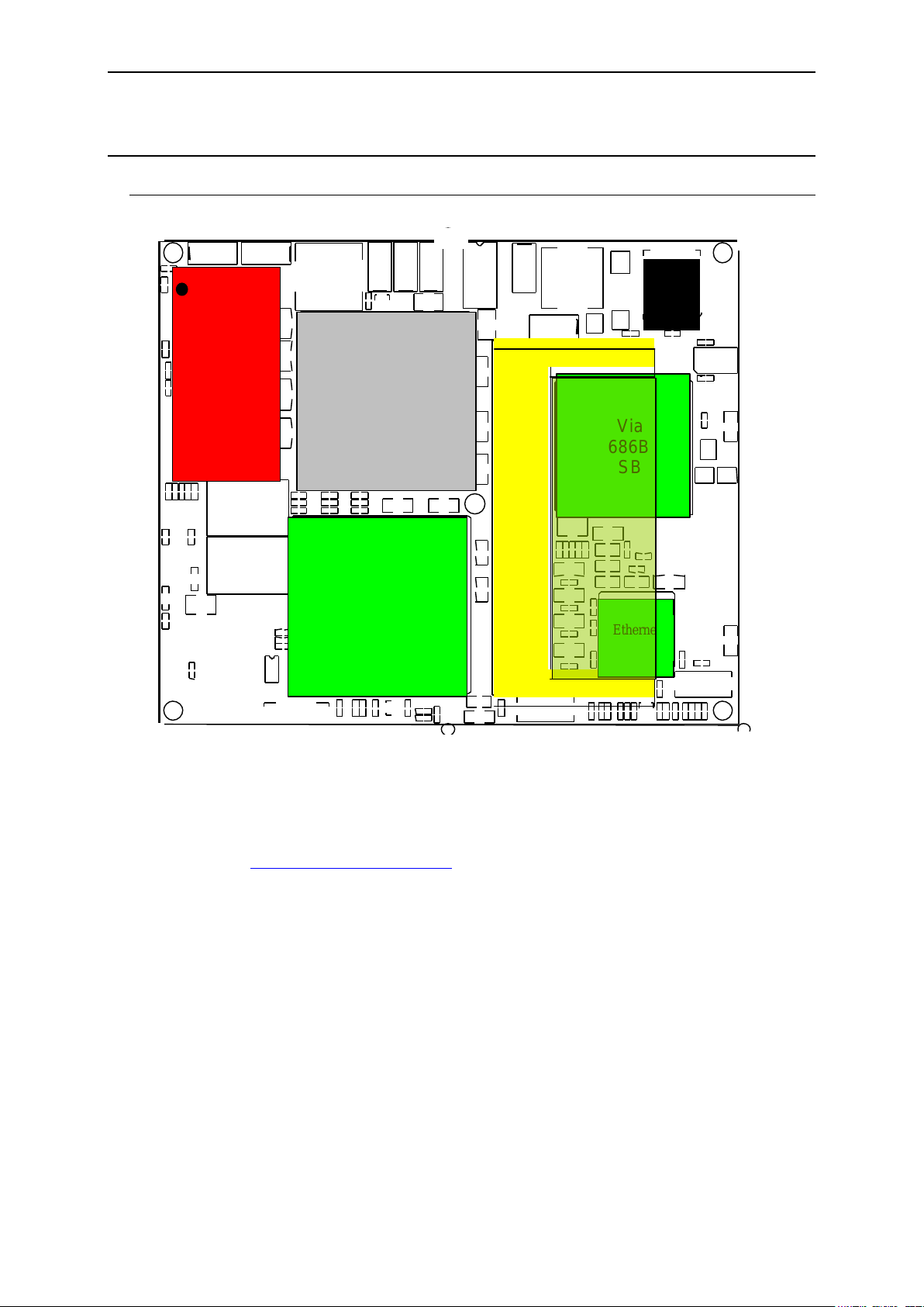
Via
C3
CPU
ATA
Disk
Chip
Via
PN133T
NB
Via
686B
SB
SDRAM
SODIMM
Pin1
Ethernet
BIOS
BOARD LAYOUT
TOP SURFACE OF THE PCB
Figure 1. BCT-ETX-C3-XXX PCB - Top View Main Component Positions.
See the section "BCT-ETX-C3-XXX Connectors " for details of individual signals on the connectors.
Page 16
BCT-ETX-C3-XXX SINGLE BOARD COMPUTER INSTALLATION
INSTALLATION
MOUNTING
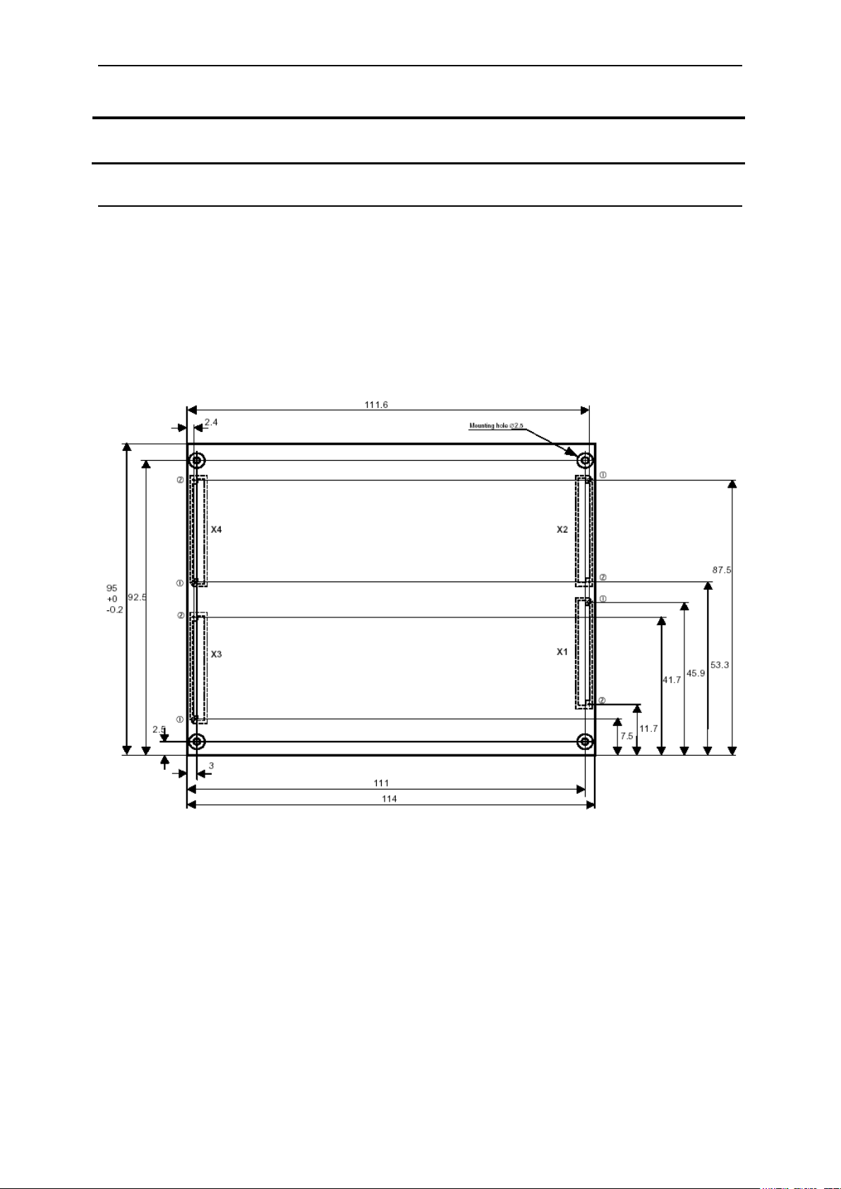
The BCT-ETX-C3-XXX board has 4 mounting holes of 2.5mm diameter. Care should be taken on the
underside of the board to not cause any mechanical damage to the components adjacent to the mounting holes.
All connections to the BCT-ETX-C3-XXX CPU are made through connectors X1-X4 inclusive. These Hirose
plug connectors (Part Number FX8-100P-SV) mate with corresponding Hirose socket connectors (Part
Number FX8-100S-SV). When installing or removing the BCT-ETX-C3-XXX module into the target base
board, ensure all power has been removed. This includes the 5volt supply, the 5V stand-by supply and the
external Lithium cell or RTC back-up battery.
Figure 2. BCT-ETX-C3-XXX PCB - Top View Showing Mounting Hole Positions.
All Dimensions in millimetres
Please note that the spacing/alignment for the ETX module connectors and the baseboard connectors differs by
0.6mm.
Where the spacing of X1 and X2 from X3 and X4 is 109.2mm on the module (111.6-2.4), it is 109.8mm (111.9-
2.1) on the baseboard. This is due to a different offset between pegs and connector aperture in the two mating
connectors.
Included in our reference design pack is a DXF file of our Evaluation Backplane for this reason.
Also note that bookmarks 1 and 2 in our diagram indicate 1.1 and 0.7 mm holes for the pegs – adjacent to pins 1
and 99 on the connectors.
Page 17
BCT-ETX-C3-XXX SINGLE BOARD COMPUTER INSTALLATION
THERMAL PLATE
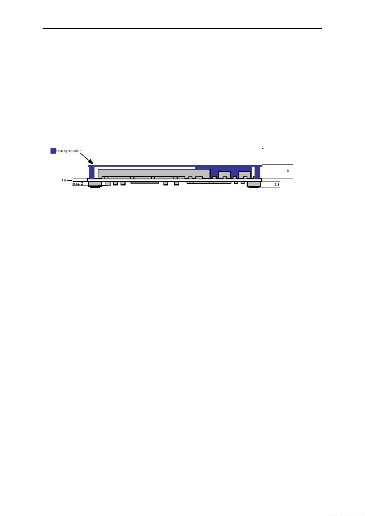
The BCT-ETX-C3-XXX Module has been designed to operate in conjunction with a thermal heat-spreading
plate. This 2mm thick aluminium plate is designed to assist in the cooling solution by providing a uniform
thermal interface which thermally couples to the heat generating components of the BCT-ETX-C3-XXX, namely
the North Bridge chip and the CPU itself. This uniform thermal interface allows the user to apply an appropriate
cooling solution such as a fan, heat-sink, heat-pipe or chassis fixing. The heat-spreader plate is not a heat-sink
but may provide adequate cooling for lower power CPUs running non-CPU intensive applications . Clearance
slots in the heat spreader plate permit the user access the SODIMM and ATA Disk Chip Socket for upgrading
the system.
Page 18

BCT-ETX-C3-XXX SINGLE BOARD COMPUTER INSTALLATION
Pin Number
Signal
Pin Number
Signal
1
GND
2
GND
3
PCICLK3
4
PCICLK4
5
GND
6
GND
7
PCICLK1
8
PCICLK2
9
REQ3#
10
GNT3#
11
GNT2#
12
3V
13
REQ2#
14
GNT1#
15
REQ1#
16
3V
17
GNT0#
18
NC
19
VCC
20
VCC
21
SERIRQ
22
REQ0#
23
AD0
24
3V
25
AD1
26
AD2
27
AD4
28
AD3
29
AD6
30
AD5
31
CBE0#
32
AD7
33
AD8
34
AD9
35
GND
36
GND
37
AD10
38
AUXAL
39
AD11
40
MIC
41
AD12
42
AUXAR
43
AD13
44
ASVCC
45
AD14
46
SNDL
47
AD15
48
ASGND
49
CBE1#
50
SNDR
51
VCC
52
VCC
53
PAR
54
SERR#
55
PERR#
56
NC
57
PME#
58
USB2#
59
LOCK#
60
DEVSEL#
61
TRDY#
62
USB3#
63
IRDY#
64
STOP#
65
FRAME#
66
USB2
67
GND
68
GND
69
AD16
70
CBE#2
71
AD17
72
USB3
73
AD19
74
AD18
75
AD20
76
USB0#
77
AD22
78
AD21
79
AD23
80
USB1#
81
AD24
82
CBE3#
83
VCC
84
VCC
85
AD25
86
AD26
87
AD28
88
USB0
89
AD27
90
AD29
91
AD30
92
USB1
93
PCIRST#
94
AD31
95
INTC#
96
INTD#
97
INTA#
98
INTB#
99
GND
100
GND
CONNECTOR PIN ASSIGNMENT
Connector X1
Page 19

BCT-ETX-C3-XXX SINGLE BOARD COMPUTER INSTALLATION
Pin Number
Signal
Pin Number
Signal
1
GND
2
GND 3 SD14
4
SD15
5
SD13
6
MASTER#
7
SD12
8
DREQ7
9
SD11
10
DACK7#
11
SD10
12
DREQ6
13
SD9
14
DACK6#
15
SD8
16
DREQ5
17
MEMW#
18
DACK5#
19
MEMR#
20
DREQ0
21
LA17
22
DACK0#
23
LA18
24
IRQ14
25
LA19
26
IRQ15
27
LA20
28
IRQ12
29
LA21
30
IRQ11
31
LA22
32
IRQ10
33
LA23
34
IOCS16#
35
GND
36
GND
37
SBHE#
38
MEMCS16#
39
SA0
40
OSC
41
SA1
42
BALE
43
SA2
44
TC
45
SA3
46
DACK2#
47
SA4
48
IRQ3
49
SA5
50
IRQ4
51
VCC
52
VCC
53
SA6
54
IRQ5
55
SA7
56
IRQ6
57
SA8
58
IRQ7
59
SA9
60
SYSCLK
61
SA10
62
REFRESH#
63
SA11
64
DREQ1
65
SA12
66
DACK1#
67
GND
68
GND
69
SA13
70
DREQ3
71
SA14
72
DACK3#
73
SA15
74
IOR#
75
SA16
76
IOW#
77
SA18
78
SA17
79
SA19
80
SMEMR#
81
IOCHRDY
82
AEN
83
VCC
84
VCC
85
SD0
86
SMEMW#
87
SD2
88
SD1
89
SD3
90
0WS#
91
DREQ2
92
SD4
93
SD5
94
IRQ9
95
SD6
96
SD7
97
IOCHCK#
98
RSTDRV
99
GND
100
GND
Connector X2
Page 20
BCT-ETX-C3-XXX SINGLE BOARD COMPUTER INSTALLATION
Pin Number
Signal
Pin Number
Signal
1
GND
2
GND 3 RED
4
BLUE
5
HSYNC
6
GREEN
7
VSYNC
8
DDCK
9
DETECT#
10
DDDA
11
2ND LVDSCLK#/B4
12
SHFCLK
13
2ND LVDSCLK/B5
14
EN
15
GND
16
GND
17
2ND LVDS 1/B1
18
2ND LVDS2/B3
19
2ND LVDS1#/B0
20
2ND LVDS2#/B2
21
GND
22
GND
23
G2
24
2ND LVDS0/G5
25
G3
26
2ND LVDS0#/G4
27
GND
28
GND
29
1ST LVDS2#/R4
30
1ST LVDSCLK/G1
31
1ST LVDS2/R5
32
1ST LVDSCLK#/G0
33
GND
34
GND
35
1ST LVDS0/R1
36
1ST LVDS1/R3
37
1ST LVDS0#/R0
38
1ST LVDS1#/R2
39
VCC
40
VCC
41
I2CDAT
42
LTGIO/FLM
43
I2CCLK
44
BLON#
45
BIASON/LP
46
DIGON
47
NC
48
NC
49
NC
50
NC
51
LPT/FLPY#
52
NC
53
VCC
54
GND
55
STB#/RSVD
56
AFD#/DENSEL
57
RSVD
58
RSVD
59
IRRX
60
ERR#/HDSEL#
61
IRTX
62
PD6/RSVD
63
RXD2
64
INIT#/DIR#
65
GND
66
GND
67
RTS2#
68
PD5/RSVD
69
DTR2#
70
SLIN#/STEP#
71
DCD2#
72
PD4/DSKCHG#
73
DSR2#
74
PD3/RDATA#
75
CTS2#
76
PD2/WP#
77
TXD2
78
PD1/TRK0#
79
RI2#
80
PD0/INDEX#
81
VCC
82
VCC
83
RXD1
84
ACK#/DRV
85
RTS1#
86
BUSY#/MOT
87
DTR1#
88
PE/WDATA#
89
DCD1#
90
SLCT#/WGATE#
91
DSR1#
92
MSCLK
93
CTS1#
94
MSDAT
95
TXD1
96
KBCLK
97
RI1#
98
KBDAT
99
GND
100
GND
Connector X3
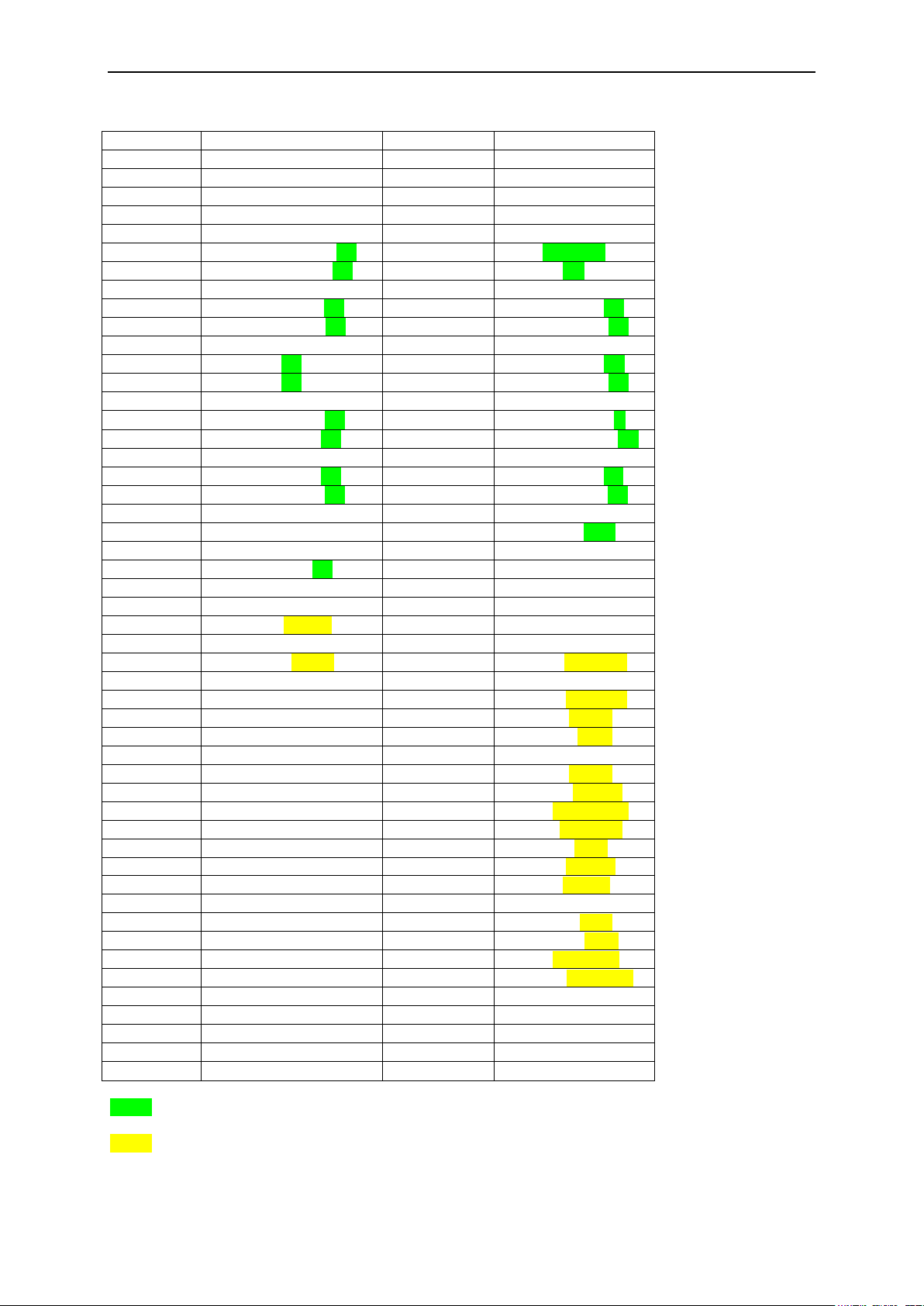
NOTE: These signals are the definition for the LCD build version of the BCT-ETX-C3-XXX
NOTE: These signals are the definition when signal LPT/FLPY# (Pin51 of X3) is pulled low at power on.
Page 21

BCT-ETX-C3-XXX SINGLE BOARD COMPUTER INSTALLATION
Pin Number
Signal
Pin Number
Signal
1
GND
2
GND 3 5VSB
4
PWRGDIN
5
PSON
6
SPEAKER
7
PWRBTN#
8
BATT
9
KBINH
10
LILED
11
RSMRST#
12
ACTLED
13
RSVD
14
SPEEDLED
15
RSVD
16
I2CLK
17
VCC
18
VCC
19
OVCR#
20
RSVD
21
EXTSMI#
22
I2DAT
23
SMBCLK
24
SMBDATA
25
SIDE_CS3#
26
SMBALERT#
27
SIDE_CS1#
28
DASP_S
29
SIDE_A2
30
PIDE_CS3#
31
SIDE_A0
32
PIDE_CS1#
33
GND
34
GND
35
PDIAG_S
36
PIDE_A2
37
SIDE_A1
38
PIDE_A0
39
SIDE_IRQ
40
PIDE_A1
41
BATLOW#
42
SIDE_33/66#
43
SIDE_AK#
44
PIDE_IRQ
45
SIDE_RDY
46
PIDE_AK#
47
SIDE_IOR#
48
PIDE_RDY
49
VCC
50
VCC
51
SIDE_IOW#
52
PIDE_IOR#
53
SIDE_DRQ
54
PIDE_IOW#
55
SIDE_D15
56
PIDE_DRQ
57
SIDE_D0
58
PIDE_D15
59
SIDE_D14
60
PIDE_D15
61
SIDE_D1
62
PIDE_D15
63
SIDE_D13
64
PIDE_D15
65
GND
66
PIDE_D15
67
SIDE_D2
68
PIDE_D15
69
SIDE_D12
70
PIDE_D15
71
SIDE_D3
72
PIDE_D15
73
SIDE_D11
74
PIDE_D15
75
SIDE_D4
76
PIDE_D15
77
SIDE_D10
78
PIDE_D15
79
SIDE_D5
80
PIDE_D15
81
VCC
82
VCC
83
SIDE_D9
84
PIDE_D5
85
SIDE_D6
86
PIDE_D9
87
SIDE_D8
88
PIDE_D6
89
RING#
90
PIDE_33/66#
91
RXD#
92
PIDE_D8
93
RXD
94
SIDE_D7
95
TXD#
96
PIDE_D7
97
TXD
98
HDRST#
99
GND
100
GND
Connector X4
Page 22

BCT-ETX-C3-XXX SINGLE BOARD COMPUTER INSTALLATION
Signal Descriptions
Connector X1 (PCI-Bus, USB, Sound)
GND
Ground. All the GND pins on the BCT-ETX-C3-XXX module should be connected to the baseboard ground
plane.
VCC
+5V 5% power supply. All VCC pins on the BCT-ETX-C3-XXX module should be connected to the
baseboard +5V plane.
3V
+3.3V 5% supply voltage generated onboard the ETX module. These three pins may be used as a
power supply for external devices. The maximum permissible current drawn collectively from these pins is
500mA.
NOTE: Do not connect 3.3V pins to an external 3.3V supply.
RSVD
These pins are reserved for future use or for manufacturing and test purposes. Do not connect
external signals to these pins.
All signals are 3.3V level PCI signals referenced to and tolerant of 5V signals. All the required PCI signal pullups are integrated on the BCT-ETX-C3-XXX board and are connected to either a 3.3V or 5V supply, as detailed
in the PCI specification. Any external PCI devices that have “5V tolerance” pins should have these pins
connected to an appropriate 5V reference voltage as per the manufacturer’s recommendation.
PCICLK1..4
PCI clock outputs for up to 4 external PCI slots or devices.
The baseboard designer should route these clocks for 1300pS total delay from the BCT-ETX-C3-XXX connector
pin to the clock pin of the PCI device.
REQ[0..3]#
Bus Request signals for up to 4 external bus mastering PCI devices. When asserted, a PCI device is requesting
PCI bus ownership from the arbiter.
GNT[0..3]#
Grant signals to PCI Masters. When asserted by the arbiter, the requesting PCI master has been granted
ownership of the PCI bus.
AD[0..31]
PCI Address and Data Bus Lines. These multiplexed lines carry the address and data information for PCI
transactions. A Bus transaction consists of an Address phase followed by one or more Data phases.
CBE[0..3]#
PCI Bus Command and Byte Enables. Bus command and byte enables are multiplexed in these
lines for address and data phases, respectively.
PAR
Parity bit for the PCI bus. Generated as even parity across AD[31:0] and CBE[3:0]#.
SERR#
System Error. This signal reports address parity errors, data errors on special cycles or any other system error
where the result will be catastrophic.
GPERR#
Parity Error. This signal reports data parity errors on all bus transaction except special cycles.
PME#
Power management event.
LOCK#
Lock Resource Signal. This pin indicates that either the PCI master or the bridge intends to run exclusive
transfers.
DEVSEL#
Device Select. When the target device has decoded the address as its own cycle, it will assert DEVSEL#.
TRDY#
Target Ready. This pin indicates that the target is ready to complete the current data phase of a transaction.
IRDY#
Initiator Ready. This signal indicates that the initiator is ready to complete the current data phase of a
transaction.
STOP#
Stop. This signal indicates that the target is requesting that the master to stop the current transaction.
Page 23

BCT-ETX-C3-XXX SINGLE BOARD COMPUTER INSTALLATION
FRAME#
Cycle Frame of PCI Buses. This indicates the beginning and duration of a PCI access. The access will be either
an output driven by the Northbridge on behalf of the CPU, or an input during PCI master access.
PCIRST#
PCI Bus Reset. This is an output signal to reset the entire PCI Bus. This signal is asserted
during system reset.
INTA#, INTB#, INTC#, INTD#
PCI interrupts. These interrupts are sharable and are typically wired in rotation to PCI slots or
devices.
IDSEL
This pin is not present on the ETX module connector, but it is present on each PCI slot connector or device.
IDSEL is an input to the device that is used to set the device’s configuration address for PCI configuration
cycles. The IDSEL pin of each device is typically connected to one of the AD lines in order to set a unique
configuration address. In ETX systems, the four external bus slots or devices are assumed to use AD[19..22] for
IDSEL connections.
USB Signals
USB signal termination components are integrated on the ETX board. In applications using external USB
devices, baseboard designers will typically include USB protection components on the baseboard, including
power supply current limiting or fusing components. USB data signals should be routed as differential pairs.
USB0, USB0#
Universal Serial Bus Port 0. These are the serial differential data pairs for USB Port 0. USB0 – positive signal.
USB0# – negative signal.
USB1, USB1#
Universal Serial Bus Port 1. These are the serial differential data pairs for USB Port 1. USB1 – positive signal.
USB1# – negative signal.
USB2, USB2#
Universal Serial Bus Port 2. These are the serial differential data pairs for USB Port 2. USB2 – positive signal.
USB2# – negative signal.
USB3, USB3#
Universal Serial Bus Port 3. These are the serial differential data pairs for USB Port 3. USB3 – positive signal.
USB3# – negative signal.
Audio Signals
SNDL/ SNDR
Line-level stereo output left/ right. These outputs have a nominal level of 1 volt RMS into a 10K impedance
load. These outputs cannot drive low-impedance speakers directly.
AUXAL/ AUXAR
Auxiliary A input left/ right. Normally intended for connection to an internal or external CDROM analog output
or a similar line-level audio source. Minimum input impedance is 5KOhm.
Nominal input level is 1 volt RMS.
MIC
Microphone input. Minimum input impedance is 5KOhm, max. input voltage is 0.15 Vpk-pk.
ASGND
Analog ground for sound controller. Use this signal ground for an external amplifier in order to achieve lowest
audio noise levels.
ASVCC
Analog supply voltage for sound controller. This is an output which is used for production test only. Do not
make external connections to this pin.
Miscellaneous
SERIRQ
Serial interrupt request. This pin is used to support the serial interrupt protocol.
Page 24

BCT-ETX-C3-XXX SINGLE BOARD COMPUTER INSTALLATION
Connector X2
ISA Signals
All required signal pull-ups are integrated into the BCT-ETX-C3-XXX module. In some applications it may be
desirable to add additional signal termination components to the baseboard.
SD[0..15]
These signals provide data bus bits 0 to 15 for any peripheral devices. All 8-bit devices use SD0[0..7] for data
transfers. 16-bit devices use SD[0..15]. To support 8-bit devices, the data on SD[8..15] is gated to SD[0..7]
during 8-bit transfers to these devices. 16-bit CPU cycles will be automatically converted into two 8-bit cycles
for 8-bit peripherals.
SA[0..19]
Address bits 0 through 15 are used to address I/O devices. Address bits 0 through 19 are used to address memory
within the system. These 20 address lines, in addition to LA[17..23] allow access of up to 16MB of memory.
SA[0..19] are gated on the ISA-bus when BALE is high and latched on to the falling edge of BALE.
SBHE#
Bus High Enable indicates a data transfer on the upper byte of the data bus SD[8..15]. 16-bit I/O devices use
SBHE# to enable data bus buffers on SD[8..15].
BALE
BALE is an active-high pulse generated at the beginning of any bus cycle initiated by a CPU module. It indicates
when the SA[0..19], LA17.23, AEN, and SBHE# signals are valid.
AEN
AEN is an active-high output that indicates a DMA transfer cycle. Only resources with a active DACK# signal
should respond to the command lines when AEN is high.
MEMR#
MEMR# instructs memory devices to drive data onto the data bus. MEMR# is active for all memory read cycles.
SMEMR#
SMEMR# instructs memory devices to drive data onto the data bus. SMEMR# is active for memory read cycles
to addresses below 1MB.
MEMW#
MEMW# instructs memory devices to store the data present on the data bus. MEMW# is active for all memory
write cycles.
SMEMW#
SMEMW# instructs memory devices to store the data present on the data bus. SMEMW# is active for all
memory write cycles to address below 1MB.
IOR#
I/O read instructs an I/O device to drive its data onto the data bus. It may be driven by the CPU or by the DMA
controller. IOR# is inactive (high) during refresh cycles.
IOW#
I/O write instructs an I/O device to store the data present on the data bus. It may be driven by the CPU or by the
DMA controller. IOW# is inactive (high) during refresh cycles.
IOCHK#
IOCHK# is an active-low input signal that indicates that an error has occurred on the module bus. If I/O
checking is enabled on the CPU module, an IOCHK# assertion by a peripheral device sends a NMI to the
processor.
IOCHRDY
The I/O Channel Ready is pulled low in order to extend the read or write cycles of any bus access when required.
The CPU, DMA controllers or refresh controller can initiate the cycle. Any peripheral that cannot present read
data or strobe in write data within this amount of time use IOCHRDY to extend these cycles. This signal should
not be held low for more than 2.5 s for normal operation. Any extension to more than 2.5 s does not guarantee
proper DRAM memory content due to the fact that memory refresh is disabled while IOCHRDY is low.
MEMCS16#
The MEMCS16# signal determines when a 16-bit to 8-bit conversion is needed for memory bus cycles. A
conversion is done any time the CPU module requests a 16-bit memory cycle while the MEMCS16# line is high.
If MEMCS16# is high, 16-bit CPU cycles are automatically converted on the bus into two 8-bit cycles. If
MEMCS16# is low, an access to peripherals is performed 16 bits wide.
Page 25

BCT-ETX-C3-XXX SINGLE BOARD COMPUTER INSTALLATION
IOCS16#
The IOCS16# signal determines when a 16-bit to 8-bit conversion is needed for I/O bus cycles. A conversion is
done any time the CPU module requests a 16-bit I/O cycle while the IOCS16# line is high. If IOCS16# is high,
16-bit CPU cycles are automatically converted on the bus into two 8-bit cycles. If IOCS16# is low, an access to
peripherals is performed 16 bits wide.
REFRESH#
REFRESH# is pulled low whenever a refresh cycle is initiated. A refresh cycle is activated every 15.6 us in order
to prevent loss of DRAM data.
0WS#
The Zero wait state signal tells the CPU to complete the current bus cycle without inserting the default wait
states. By default the CPU inserts 4 wait states for 8-bit transfers and 1 wait state for 16-bit transfers.
MASTER#
This signal is used with a DRQ line to gain control of the system bus. A processor or a DMA controller on the
I/O channel may issue a DRQ to a DMA channel in cascade mode and receive a DACK#. Upon receiving the
DACK#, a bus master may pull MASTER# low, which will allow it to control the system address, data and
control lines. After MASTER# is low, the bus master must wait one system clock period before driving the
address and data lines, and two clock periods before issuing a read or write command. If this signal is held low
for more than 15 us, system memory may be lost as memory refresh is disabled during this process.
SYSCLK
SYSCLK is supplied by the CPU module and has a nominal frequency of about 8 MHz with a duty cycle of 4060 percent. The frequency supplied by different CPU modules may vary. This signal is supplied at all times
except when the CPU module is in sleep mode.
OSC
OSC is supplied by the CPU module. It has a nominal frequency of 14.31818 MHz and a duty
cycle of 40-60 percent. This signal is supplied at all times except when the CPU module is in
sleep mode.
RESETDRV
This active-high output is system reset generated from CPU modules. It is responsible for
resetting external devices on the ISA Bus.
DREQ[0, 1, 2, 3, 5, 6, 7]
The asynchronous DMA request inputs are used by external devices to indicate when they need service from the
CPU modules DAM controllers. DREQ0..3 are used for transfers between 8-bit I/O adapters and system
memory. DREQ5..7 are used for transfers between 16-bit I/O adapters and system memory. DRQ4 is not
available externally. All DRQ pins have pull-up resistors on the CPU modules.
DACK[0, 1, 2, 3, 5, 6, 7]#
DMA acknowledge 0..3 and 5.7 are used to acknowledge DMA requests. They are active-low.
TC
The active-high output Terminal Count indicates that one of the DMA channels has transferred all data.
IRQ[3..7, 9,15]
These are the asynchronous interrupt request lines. IRQ0, 1, 2 and 8 are not available as external interrupts
because they are used internally on the CPU module. All IRQ signals are active-high. The interrupt requests are
prioritized. IRQ9 through IRQ12 and IRQ14 through IRQ15 have the highest priority (IRQ9 is the highest).
IRQ3 through IRQ7 have the lowest priority (IRQ7 is the lowest). An interrupt request is generated when an IRQ
line is raised from low to high. The line must be held high until the CPU acknowledges the interrupt request
(interrupt service routine).
Page 26

BCT-ETX-C3-XXX SINGLE BOARD COMPUTER INSTALLATION
Connector X3
VGA Signals
HSYNC
Horizontal Sync: This output supplies the horizontal synchronization pulse to the CRT monitor.
VSYNC
Vertical Sync: This output supplies the vertical synchronization pulse to the CRT monitor.
Red, Green, Blue
Red, green and blue analog video output signals for CRT monitors. These lines should be terminated with 75
ohms to ground at the video connector.
DDCK, DDDA
These two pins can be used for a DDC interface between the graphics controller chip and the CRT monitor.
LVDS Flat Panel Interface Signals
NOTE: The BCT-ETX-C3-XXX.module is available with either LVDS or 18 bit direct drive LCD STN/TFT
interface. This option must be specified at the time of purchase. The BCT-ETX-C3-XXX does not support 24 bit
panels in either LVDS or direct drive LCD options
1stLVDS0, 1stLVDS0#
1st LVDS Channel, link0 differential pairs LCD data output. These signals are differential and should be routed
as differential pairs. 1stLVDS0# is the complement of 1stLVDS0.
1stLVDS1, 1stLVDS1#
As above, link1.
1stLVDS2, 1stLVDS2#
As above, link2.
1stLVDSCLK, 1stLVDSCLK#
As above, clock link.
2nd LVDS0, 2nd LVDS0#
2nd LVDS Channel, link0 differential pairs LCD data output. These signals are differential and should be routed
as differential pairs. 2ndLVDS0# is the complement of 2ndLVDS0.
2nd LVDS1, 2nd LVDS1#
As above, link1.
2nd LVDS2, 2nd LVDS2#
As above, link2.
2ndLVDSCLK, 2ndLVDSCLK#
As above, clock link.
Single channel LVDS link is use the first channel only. Dual channel links, which are
commonly used to transmit higher data rates, will use both the first and second channels.
The Txout3 and Txout3# for both first and second channels are not supported by the BCTETX-C3-XXX board.
PIN NAME LVDS SIGNAL CHANNEL
1st LVDS0# Txout0# first
1st LVDS 0 Txout0 first
1st LVDS1# Txout1# first
1st LVDS 1 Txout1 first
1st LVDS2# Txout2# first
1st LVDS 2 Txout2 first
1st LVDSCLK# Txclock# first
1st LVDSCLK Txclock first
2nd LVDS0# Txout0# second
2nd LVDS0 Txout0 second
2nd LVDS1# Txout1# second
2nd LVDS1 Txout1 second
2nd LVDS2# Txout2# second
2nd LVDS2# Txout2 second
2nd LVDSCLK# Txclock# second
2nd LVDSCLK Txclock second
Page 27

BCT-ETX-C3-XXX SINGLE BOARD COMPUTER INSTALLATION
BIASON
Controls panel contrast voltage.
DIGON
Controls panel digital power.
BLON#
Controls back-light power.
LTGIO0
General purpose I/O pin.
I2CLK, I2DAT
I2C interface for panel parameter EEPROM. This EEPROM is mounted on the LVDS receiver. The data in the
EEPROM allows the ETX module to automatically set the proper timing parameters for a specific LCD panel.
DETECT#
Panel hot-plug detection. Implementation of this pin is optional. See the specific ETX module product manual
for details.
LCD Interface Signals
NOTE: ETX modules may implement either this parallel interface or the LVDS flat panel interface described
above. This pin implementation depends on which BCT-ETX-C3 variant is being used ie LVDS or LCD
R[0..5], G[0..5], B[0..5]
Parallel digital signals for red, green and blue pixel data.
LP( Line/Latch Pulse)
Horizontal Sync: This output supplies the horizontal synchronisation pulse for flat panels.
FLM ( First Lime Marker)
This output supplies the vertical synchronisation pulse for flat panels.
DE
Data enable signal. Usage depends on display type.
SHCLK
Panel data clock signal.
DETECT#
Panel hot-plug detection.
Serial Port Signals
Note: that all serial port signals on the ETX module connectors are logic level signals. External transceiver
devices are necessary for the conversion of the logic level signals to the desired physical interface such as
RS232, RS422, or RS485.
DTR1#, DTR2#
Active-low data terminal ready outputs for the serial port. Handshake output signal notifies the modem that the
UART is ready to establish a data communication link.
RI1#, RI2#
Active-low input is for the serial port. Handshake signals notify the UART when a telephone ring signal is
detected by the modem.
TXD1, TXD2
Transmitter serial data output from serial port.
RXD1, RXD2
Receiver serial data input.
CTS1#, CTS2#
Active-low input for serial ports. Handshake signals notify the UART when the modem is ready to receive data.
RTS1#, RTS2#
Active-low output for serial port. Handshake signals notify the modem when the UART is ready to transmit data.
DCD1#, DCD2#
Active-low input for serial port. Handshake signals notify the UART when a carrier signal is
detected by the modem.
DSR1#, DSR2#
This active-low input is for serial port. Handshake signals are use to notify the UART that the
modem is ready to establish the communication link.
PS/2 Keyboard, PS/2 Mouse Signals
KBDAT
Bi-directional keyboard data signal.
Page 28

BCT-ETX-C3-XXX SINGLE BOARD COMPUTER INSTALLATION
KBCLK
Keyboard clock signal.
MSDAT
Bi-directional mouse data signal.
MSCLK
Mouse clock signal.
IRDA (SIR) Signals
IRTX, IRRX
Infrared transmit and receive pins.
Parallel Port Signals
The parallel port signals require external termination components. The parallel port has two alternative operating
modes: parallel port and floppy disk. If the parallel port is used in parallel port mode, floppy disk support is not
available via the parallel port. The LPT/FLPY# pin, which switches the parallel port modes, is sensed only at
boot and cannot be changed dynamically. If simultaneous floppy drive and parallel support is needed, an external
floppy controller may be incorporated in the baseboard design.
LPT/FLPY#
This ETX input signal selects whether the parallel port pins will implement parallel port or floppy support
functionality. There is an internal pullup on this signal. If this signal is high or unconnected, the following
parallel port pin functions are in effect:
STB#
This active-low signal is used to strobe the printer data into the printer.
AFD#
This active-low output tells the printer to automatically feed the next single line after each preceding line has
been printed.
PD[0..7]
This bi-directional parallel data bus is used to transfer information between the CPU and the peripherals.
ERR#
This active-low signal indicates an error situation has occurred at the printer.
INIT#
This active-low signal is used to initiate the printer when low.
SLIN#
This active-low signal selects the printer.
ACK#
This active-low output from the printer indicates that it has received the previous data and that it is ready to
receive new data.
BUSY#
This signal indicates that the printer is busy and not ready to receive new data.
PE
This signal indicates that the printer is out of paper.
SLCT#
This active-high output from the printer indicates that its power is on.
Floppy Signals
ETX modules support only a single floppy drive over the parallel port interface. When operating in floppy disk
mode, the parallel port is not available.
LPT/FLPY#
This ETX input signal selects whether the parallel port pins will implement parallel port or floppy support
functionality. There is an internal pullup on this signal. If this signal is low, the following floppy support
functions are supported over the parallel port pins:
DENSEL
Indicates whether a low (250/300Kb/s) or high (500/1000Kbs) data rate has been selected.
INDEX#
This active-low Schmitt Trigger input signal is asserted by the disk drive when the diskette index hole is sensed.
TRK0#
This active-low Schmitt Trigger input signal is asserted by the disk drive when the head is positioned over the
outermost track.
WP#
This active-low Schmitt Trigger input signal is asserted by the disk drive when a disk is write-protected.
Page 29

BCT-ETX-C3-XXX SINGLE BOARD COMPUTER INSTALLATION
RDATA#
The active-low, raw-data read signal from the disk drive. Each falling edge represents a flux transition of the
encoded data.
DSKCHG#
This active-low input signal is asserted by the disk drive when the drive door has been opened.
DRV
This signal selects the floppy drive.
MOT
This active-low output activates the disk drive motor.
HDSEL#
This active-low output determines which disk drive head is active. Low = Head 0. High (open) = Head 1.
DIR#
This active-low output determines the direction of head movement (low = step-in, high = stepout).
STEP#
This active-low output signal is pulsed at a software-programmable rate to move the head during a seek
operation.
WDATA#
This active-low output is a write pre-compensated serial data stream to be written onto the selected disk drive.
Each falling edge causes a flux change on the media.
WGATE#
This active-low output enables the write circuitry of the selected disk drive.
Connector X4
IDE Signals
IDE signals are duplicated for the Primary and Secondary IDE channels. For each signal, the
first signal name is for the primary channel and the second signal name is for the secondary
channel.
PIDE_D0..15/ SIDE_D0..15
IDE Data Bus.
PIDE_A[0..2]/ SIDE_A[0..2]
IDE Address Bus.
PIDE_CS1#/ SIDE_CS1#
IDE Chip Select 1. This is the Chip Select 1 command output pin that enables the IDE device to watch the
Read/Write Command.
PIDE_CS3#/ SIDE_CS3#
IDE Chip Select 3. This is the Chip Select 3 command output pin that enables the IDE device to watch the
Read/Write Command.
PIDE_DRQ/ SIDE_DRQ
IDE DMA Request for IDE Master. This signal is asserted by an IDE device. It will be active-high in DMA or
Ultra-33 mode and always be inactive-low in PIO mode.
PIDED_AK#/ SIDED_AK#
IDE DACK# for IDE Master. This signal grants the IDE DMA request to begin the IDE Master Transfer in
DMA or Ultra-33 mode.
PIDE_RDY/ SIDE_RDY
IDE Ready. This is the input pin from the IDE Channel. It indicates that the IDE device is ready to terminate the
IDE command in PIO mode. The IDE device can de-assert this input to expand the IDE command if the device is
not ready. In Ultra-33 mode, this pin has different functions.
PIDE_IOR#/ SIDE_IOR#
IDE IOR# Command. This is the IOR# command output pin used to tell the IDE device to assert the Read Data
in PIO and DMA mode. In Ultra-33 mode, this pin has different functions.
PIDE_IOW#/ SIDE_IOW#
IDE IOW# Command. This is the IOW# command output pin used to notify the IDE device that the available
Write Data is already asserted by the IDE Busmaster in PIO and DMA mode. In Ultra-33 mode, this pin has
different functions.
PIDE_INTRQ/ SIDE_INTRQ
Interrupt request signal from the IDE device.
HDRST#
Low-active hardware reset (RSTDRV inverted).
DASP_S
Time-multiplexed, open collector output that indicates that a drive is active. Also used for
Page 30

BCT-ETX-C3-XXX SINGLE BOARD COMPUTER INSTALLATION
Master/Slave negotiation on the Secondary IDE channel. If an IDE device such as a Flash Disk exists onboard
the ETX module, this signal must be connected to the DASP_S pin of any other device connected to the
Secondary IDE channel.
PDIAG_S
The signal is used for Master/Slave negotiation on the Secondary IDE channel. It is asserted by the Slave to
indicate to a master that the slave has passed its internal Diagnostic command. If an IDE device such as a Flash
Disk exists onboard the ETX module, this signal must be connected to the PDIAG_S pin of any other device
connected to the Secondary IDE channel. This pin may additionally be used to detect the presence of the 80
conductor IDE cable which is required to support DMA66 or DMA100.
CBLID_P
On ETX modules that support DMA66 or DMA100, this pin may be used to detect the presence of an 80
conductor IDE cable on the primary IDE channel. This allows BIOS or system software to determine whether to
enable high-speed transfer modes.
Ethernet Signals
The ETX Ethernet Interface is designed for use with an external 1:1/ 1:1 transformer.
TXD#, TXD (ANALOG TWISTED PAIR)
Ethernet Transmit Differential Pair. These pins transmit the serial bit stream on the Unshielded Twisted Pair
(UTP) cable. The current-driven differential driver can be two-level (10BASE-T) or three-level (100BASE-TX)
signals depending on the mode of operation. These signals interface to the Ethernet cable through an isolation
transformer.
RXD#, RXD ( ANALOG TWISTED PAIR)
Ethernet Receive Differential Pair. These pins receive the serial bit stream from the isolation transformer. The bit
stream can be transmitted in either two-level (10BASE-T) or three-level (100BASE-TX) signals depending on
the mode of operation. These signals interface to the Ethernet cable through an isolation transformer.
ACTLED
The Activity LED pin indicates either transmitted or received data activity on the Ethernet port. This pin is
asserted low when activity is detected. It can sink 5mA to ground through an externalLED and a limiting resistor
to a 3.3V source.
LILED
The Link Integrity LED pin indicates link integrity. This pin is asserted low when the link is valid. It can sink
5mA to ground through an external LED and a limiting resistor to a 3.3V source.
SPEEDLED
The Speed LED pin indicates high speed operation. This LED is not supported by all ETX
boards. This pin is asserted low when a 100Mbps link is detected, and is not asserted for a
10Mbps link. It can sink 5mA to ground through an external LED and a limiting resistor to a
3.3V source.
Ethernet Transformer Specification
Turns ratio transmit: 1:1 +/- 5%
Turns ratio receive: 1:1 +/- 5%
Insertion Loss 1 to 60 MHz: max. 1 dB
Return Loss 1 to 80 MHz: max. 10 dB
Common Mode Rejection
30 to 100 MHz: max. 30 dB
100 to 500 MHz: max. 20 dB
Cross Talk 1 to 80 MHz: max. 35 dB
Hi-Pot (Pri-Sec): min. 1500VRMS
Supported Ethernet transformer (examples):
Pulse H0002
Pulse H1012T
Valor MD6301NDS1
Valor ST6118T
Bel Fuse S558-5999-46
Delta Electronics LF8200M
Page 31

BCT-ETX-C3-XXX SINGLE BOARD COMPUTER INSTALLATION
Power control signals
PWGIN
An active-high input to the ETX from an external power supply, indicating that the power is good and that the
ETX can begin booting. Usage of this signal is not required because the ETX module contains its own powergood logic. The PWGIN signal can also be used as an active-low reset input to the ETX module.
5V_SB
Power input for the internal suspend and power control circuitry. Connect to a 5V, 100mA stand-by power
source available. Should be connected to 5V supply if a standby supply is not available.
PS_ON
Active-low output from ETX module. Can be connected to the PS_ON input of an ATX power supply in order to
switch the main output. In order for this pin to function, 5V_SB must be supplied to the ETX module.
PWRBTN#
Power Button Input. Connect to GND with momentary-contact switch or open collector driver to implement
ATX power button control of PS_ON. In order for this pin to function, 5V_SB must be supplied to the ETX
module.
Power management signals
In order for these pins to function while VCC is powered down, 5V_SB must be supplied to the ETX module.
Note that these signals generally have pullup resistors to the suspend power supply inside the ETX module. Care
must be taken in interfacing these signals to logic that is powered down when 5V_SB is active.
RSMRST#
Resume Reset input. This input may be driven low by external circuitry in order to reset the
power management logic on the ETX module.
SMBALRT#
System Management Bus Alert input. May be driven low by SMB devices in order to signal an event on the SM
Bus.
BATLOW#
Battery low input. May be driven low by external circuitry to signal that the system battery is low, or may be
used to signal some other external power management event.
GPE1#
General purpose power management event input 1. May be driven low by external circuitry to signal an external
power management event. Within the ETX module, this pin is commonly connected to the chipset’s LID# input.
GPE2#
General purpose power management event input 2. May be driven low by external circuitry to signal an external
power management event. Within the ETX module, this pin is commonly connected to the chipset’s RING#
input.
EXTSMI
System management interrupt input. May be driven low by external circuitry to initiate an SMI.
Miscellaneous Signals
SPEAKER
PC speaker output signal. This logic-level signal can be connected to an external transistor in order to drive a
piezoelectric or dynamic speaker.
BATT
3V backup cell input. BATT is typically connected to a 3V lithium backup cell for RTC operation and CMOS
register non-volatility in the absence of system power. When RTC operation is not required by the application,
some ETX modules can back up CMOS contents to EEPROM so a battery is not needed.
I2CLK, I2DAT
These clock and data lines implement an I2C-bus.which supports external slave devices only. Data rate is
approximate 1-10kHz.. This interface is intended for support of EEPROMs and other simple I/O-devices
SMBDATA, SMBCLK
System Management Bus clock and data lines. May be used to support external SMBUS devices such as
temperature and battery monitoring chips. The addresses of external SMBUS devices must be chosen so they do
not conflict with addresses used internally on the ETX module.
KBINH
Keyboard Inhibit. Asserting this pin disables data input from the keyboard.
OVCR#
Page 32

BCT-ETX-C3-XXX SINGLE BOARD COMPUTER INSTALLATION
Over-current detect input. Used to monitor the USB power over-current. Pull with open collector to GND if
over-current is detected.
COOLING
Efficient cooling is essential for long and reliable operation of any electronic equipment. The VIA C3 CPU
and the VIA VT8606 IC (commonly termed the 'North Bridge') do get hot in normal operation, and in an
elevated ambient temperature will require additional cooling. Cooling requirements will vary with
application, desired operating temperature, CPU load, memory size and board orientation.
Mounting the PCB vertically will aid natural convection and create a chimney effect. Passive heatsinks are
available for the CPU and the VT8606 IC. A fan, whilst not always desirable, will provide a high degree of
cooling even for a relatively slow airflow.
Further options that may be considered are sinking heat to the chassis or enclosure, and in extreme situations
the use of a heat pipe.
The CPU is equipped with an onboard thermal diode for temperature monitoring. This diode is connected to
a system monitor within the South Bridge. The South Bridge is fitted with a thermal monitoring device can
also monitor its own temperature. A thermistor is available to monitor the temperature of critical and
potential hot spots on the board. Temperatures can be monitored in the BIOS Set-up. If you wish to monitor
these temperatures from your application please contact the Blue Chip Technology Technical Support team.
When designing an enclosure, bear in mind that the greater the volume of air that can flow through the
enclosure, the greater the cooling effect and the lower the temperature rise above the ambient air
temperature. However, the volume produced by any fan will vary with the pressure against which it has to
work. The resistance to airflow (the back-pressure on the fan) will depend upon the enclosure, the mounting
and restrictions. Therefore, when mounting and cabling the board, it is essential that the free circulation of
the cooling airflow is not impeded.
The calculation of airflow through an enclosure is not straightforward, and depends on many factors. The
method of meeting the cooling requirements will be specific for each system. Consequently, the system
builder is responsible for ensuring adequate cooling. However, interpreting airflow volumes is not intuitive.
As an aid to selecting suitable cooling, the following example is offered. A 60 mm axial fan (such as a Papst
type 612NGH) blowing over the board can supply up to 46 m3/hour when unrestricted. Restrictions to the
airflow will reduce this volume.
CABLING
Whilst the BCT-ETX-C3-XXX does not have any cables it should be remembered that when integrating into
a system that careless routing of connecting cables could affect the cooling dramatically. It will also have a
bearing on EMC. Lengths should be limited to the necessary minimum.
Please note when interfacing into the IDE interfaces on your Host Board that to achieve higher IDE
throughput than UDMA33 requires the use of a special 80-conductor IDE cable or PCB tracking that mimics
this. Using a standard 40-conductor IDE cable or “one to one” PCB tracking will force the interface to work
at a lower speed.
All applications will require a power connection. The BCT-ETX-C3-XXX board requires a 5V, and if
necessary a 5 volt standby supply for ATX support. The power connection to BCT-ETX-C3-XXX is made
through the four ETX connectors.
Power wiring to the base board should be of an adequate gauge to ensure that the voltage does not fall below
the watchdog trip point (nominally 4.75V at the watchdog).
If a 5V standby supply is not available, the terminal should be linked to +5V supply. The Ethernet controller
and much of the power-sequencing blocks in the chipset are powered from this terminal.
Page 33

BCT-ETX-C3-XXX SINGLE BOARD COMPUTER INSTALLATION
EMC ISSUES
The enclosure in which the board is mounted will have a significant effect on the electro-magnetic
compatibility of the final system. For best effect it should be electrically conducting and provide a complete
screen around the electronics. Apertures should be kept to a minimum and as small as possible. For
ventilation purposes, many small holes are far more preferable to a few large holes.
It is the maximum dimension of an aperture that governs the lowest frequency that can pass through the
enclosure (either in or out). This is irrespective of the width of the aperture. Even a narrow gap between
two sections of an enclosure can leak radio interference. Large apertures will significantly reduce the
electro-magnetic compatibility of the system.
The major contributor to EMC problems will be cables entering and leaving the enclosure. To minimise
these effects ensure that any external cables are fully screened, and that the screen is electrically connected
to the chassis. Full wire-screened cables are much more effective than those with a foil screen and drain
wire. Use metal connector shells/covers, and do not allow the external screen to pass into the enclosure.
Page 34

BCT-ETX-C3-XXX SINGLE BOARD COMPUTER INSTALLATION
IRQ
Device
Comment
0
Timer 0
Fixed
1
Keyboard
Fixed 2 8259 (2nd Int Controller)
Fixed
3
COM 2
Can be released if disabled in BIOS Set-up
4
COM 1
Can be released if disabled in BIOS Set-up
5
Soundblaster Audio
If legacy Soundblaster audio enabled in BIOS Setup else free
6
Floppy Drive
Fixed
7
LPT 1
If Floppy enabled this becomes free
8
Real Time Clock
Fixed
9
USB
Mobile. Can map elsewhere and share with another
PCI device.
If VGA interrupt enabled it is present here
10
Audio
Mobile. Can map elsewhere and share with another
PCI device
11
Ethernet
Mobile. Can map elsewhere and share with another
PCI device
12
PS/2 Mouse
If enabled in BIOS Set-up
13
Floating Point Unit
Fixed
14
Primary IDE
Fixed
15
Secondary IDE
Fixed
INTERRUPT ASSIGNMENT TABLE
Page 35

BCT-ETX-C3-XXX SINGLE BOARD COMPUTER INSTALLATION
DMA Channel
Use
Description
0
Used to be for memory refresh on early PCs. Available on ETX-C3
1
If Soundblaster is enabled in the BIOS setup this is occupied, else
available 2 Floppy
Reserved for the floppy disk controller
3
LPT
If Parallel port is setup in the BIOS to ECP mode this is occupied,
else available
4
Cascaded
Reserved for second set of DMA channels
5
Available 6
Available 7
Available
I/O Address
Description
0000 - 00lF
DMA Controller 1
0020 - 003F
Interrupt Controller 1, Master
0040 - 005F
Timer & Index registers for UMC491
0060 - 006F
8042 (Keyboard & Mouse)
0070 - 007F
Real Time Clock, NMI Mask
0080 - 008F
POST & DMA Page Register
00A0 - 00BF
Interrupt Controller 2, Slave
00C0 - 00DF
DMA Controller 2
00F0
Clear Maths Coprocessor Busy
00F1
Reset Maths Coprocessor
00F8 - 00FF
Maths Coprocessor
0100 - 010F
Watchdog, E²PROM, Byte Wide Socket & Software selection of serial ports
01F0 - 01F8
Hard (Fixed) Disk Controller
0208 - 021A
EMS Page registers (either 208 or 218, etc.)
02F8 - 02FF
Serial Port 2
0360 - 036F
Reserved
0378 - 037F
Parallel Printer Port 1
03B0 - 03DF
Video Adapter
03F0 - 03F7
Floppy Diskette Controller
03F8 - 03FF
Serial Port 1
1000 +
Can be allocated by PCI devices either onboard or on the host board
DIRECT MEMORY ACCESS CHANNELS (DMA)
I/O ADDRESS MAP (HEX)
Page 36
BCT-ETX-C3-XXX SINGLE BOARD COMPUTER INSTALLATION
Upper Memory
Use
Description
C0000 – CFFFF
VGA BIOS
Reserved
D0000 – DFFFF
Can be used for devices on the ISA bus or Shadow RAM
E0000 – FFFFF
System BIOS
Reserved
Device
PCI Interrupt
Description
Sound
-
Integrated into South Bridge (VIA 82C686B)
Ethernet
INTA
Intel 82251 device
AGP Video
INTA
Integrated into North Bridge (VIA 8606)
MEMORY ADDRESS MAP (HEX)
PERIPHERAL COMPONENT INTERCONNECT DEVICES (PCI)
Page 37

BCT-ETX-C3-XXX SINGLE BOARD COMPUTER TROUBLESHOOTING GUIDE
USING THE BOARD
BIOS SETTINGS
The board contains a custom implementation of the Phoenix BIOS 4, Revision 6.1 to suit the specific
hardware features.
Certain combinations of BIOS settings may prevent the BCT-ETX-C3-XXX from working correctly. If
problems or lock-ups are experienced on boot-up, clear the CMOS memory and restart. The default settings
will usually work in most instances. The CMOS memory is cleared using the jumper on the base board. To
clear the CMOS, switch off the power to the board, then move the jumper to the "CLR" position for a few
seconds, and then return it to its original position. The power may then be restored.
Press the keyboard <F2> key during the boot-up operation to enter the BIOS set-up screen. Various
information is available on the set-up and interpretation of the BIOS in the following files:
User Manual
Bios-Set
Bios-POS
LOADING OPERATING SYSTEMS & DRIVERS
Some operating systems provide in-built support for the chipset used on this board. It is variously known as
VIA PN133, VIA Pro-Savage, VIA Technologies VT8606/VT8231 with Intel Mobile Celeron or Intel mobile
PIII CPU.
A CD-ROM is supplied with each board, containing most common operating system drivers. Bear in mind that
suppliers continually update their drivers, so it is always a good idea to check on the Internet for later ones.
The following websites are good starting points:
www.via.com.tw
www.viatech.com
www.intel.com
For example for a fresh install of Windows 2000 or Windows Xp operating systems, drivers can be installed as
follows
First install the Via 4in1 drivers. This is done, by running the Setup.exe program, from the appropriate
directory on the BCT Support CD. Next the Video Device Drivers can be installed in a similar manner.
For Audio and Ethernet drivers, these are installed from Windows Device Manager. Highlight the required
item and select properties [highlight then click using the Right mouse button]. From the Properties page, select
the Driver Tab and then click on “update driver”. Follow the on-screen prompts, and when asked, select
Browse and direct the path to the relevant directory on the CD.
For Audio this is
/SBPC/DISKS/alu340bp3
For Ethernet this is
/SBPC/DISKS/intel82551ER
For other operating Systems, follows the method recommended by the OS Vendor
Page 38

BCT-ETX-C3-XXX SINGLE BOARD COMPUTER TROUBLESHOOTING GUIDE
PROGRAMMING THE BOARD
The board includes an EEPROM and a Watchdog, both of which are accessible either by using a special BIOS
function (Int. 50h) or by using the correct device driver for the operating system being used.
USER EEPROM
The EEPROM on the BCT-ETX-C3-XXX unit is a NM93C46 serially programmed device. It comprises
128 bytes of user programmable memory, organised as 64 x 16 bit words. The EEPROM does not have to
be completely erased before writing to a single location.
Before it can be used, the EEPROM must be enabled within the BIOS. The BIOS provides two functions to
simplify user access to the EEPROM memory, available through a software interrupt (INT 50h):
Write to Single EEPROM Location
Calling Registers: AH = 03
BL = Location (0 – 63)
DX = Write data (16-bit value)
Perform INT 50h
Return Registers: AH = 00, and Carry flag is clear if successful
AH = 02, and Carry flag is set if function valid but disabled
AH = FF, and Carry flag set if function failed
READ Single EEPROM Location
Calling Registers: AH = 04
BL = Location (0 – 63)
Perform INT 50h
Return Registers: DX = EEPROM Data
AH = 00, and Carry flag is clear if successful
AH = 02, and Carry flag is set if function valid but disabled
AH = FF, and Carry flag set if function failed
WATCHDOG FACILITY
BCT-ETX-C3-XXX includes a watchdog timer circuit, which may be used to monitor software or processor
hardware failure. The time-out period of the watchdog is fixed at 1200 milliseconds. The timer is enabled
or disabled by using the software interrupt at INT 50h.
The following code demonstrates the control of the watchdog timer.
Enable/Disable Watchdog
Calling Registers: AH = 05
AL = 01 to enable, 00 to disable
Perform INT 50h.
Return Registers: AH = 00, and Carry flag is clear if successful
AH = 02, and Carry flag is set if function valid but disabled
AH = FF, and Carry flag set if function failed
Page 39

BCT-ETX-C3-XXX SINGLE BOARD COMPUTER TROUBLESHOOTING GUIDE
Refresh Watchdog
Calling Registers: AH = 06
Perform INT 50h
Return Registers: Carry flag clear
ACCESSING SOFTWARE 'INT 50H' FUNCTIONS
Most high level languages allow access to software interrupts through a particular function call. The user
loads a particular function code into the AH register followed by a specific set of parameters in the other
registers before executing the interrupt.
For example, in C :-
#include <stdio.h>
#include <dos.h>
#define BCT-ETX-C3-XXX 0x50
void main(void)
{
union REGS regs;
regs.x.ax = 0x0400; /* read eeprom data */
regs.x.bx = 0x31; /* from address 0x31 */
int86(BCT-ETX-C3-XXX, ®s, ®s);
printf("EEPROM Address 0x31 contains %x\n",regs.x.dx);
}
and similarly in Quick Basic
'Read EEPROM Data via interrupt 50 call
$include:'QB.BI'
DIM INARY%(7), OUTARY%(7)
CONST AX=0,BX=1,CX=2,DX=3,BP=4,SI=5,DI=6,FL=7
INARY%(AX) = &H0400 ' Read e2 data
INARY%(BX) = &H31 ' address &H31
CALL INT86OLD(&H50,INARY%(),OUTARY%()) ' Call the Int50h service
PRINT "EEPROM ADDRESS &H31 CONTAINS: ";OUTARY%(DX)
Note that only the functions listed in the sections above are valid. On return, the contents of register AH
may contain a value indicating the status:
AH = 00h - Function successful, Carry flag cleared
AH = 01h - Function invalid, Carry flag set
AH = 02h - Function valid but disabled, Carry flag set
AH = 03h - Function failed, Carry flag set
Page 40

BCT-ETX-C3-XXX SINGLE BOARD COMPUTER TROUBLESHOOTING GUIDE
MAINTENANCE
The only regular maintenance required is to ensure that the cooling airflow remains unrestricted. Generally
the enclosure design and the wiring layout will ensure that the cooling is stable. However, bear in mind that
any air filters may become clogged thereby reducing the cooling.
After a period of time, it may be necessary to replace the on-board battery, if it cannot maintain the CMOS
memory.
Page 41

BCT-ETX-C3-XXX SINGLE BOARD COMPUTER TROUBLESHOOTING GUIDE
TROUBLESHOOTING GUIDE
This is not intended as an extensive faultfinding procedure, rather it is intended to indicate the more likely causes
of failure with this product. Ensure that the power is switched off before making any hardware changes. Bear in
mind that it is possible to set combinations of parameters within the BIOS that will prevent proper operation of
the board. See the BIOS section for details. If in doubt, set default values or clear the CMOS memory and start
again. Default values will generally provide a working but limited system.
SYMPTOM Fail to boot
Possible Cause Power supply incorrect
Action Check all supply rails 5V, 5V
Possible Cause Check that the 5Vstandby terminal is connected
Action Link to +5V if not powered from an ATX 5Vstandby supply
Possible Cause CMOS memory corrupt/invalid.
Action Power off, set CMOS clear jumper to 'Clear' on base board (if it exists), then return jumper
to operational position
Possible Cause CMOS Clear jumper in wrong position
Action Set to operational position, NOT 'Clear'
Possible Cause Extended System Configuration Data (ESCD) memory corrupt/invalid
Action Use BIOS Setup to clear and re-write the ESCD memory
Possible Cause Memory not fully seated in socket
Action Remove and refit memory
Possible Cause Add-in board requires other voltage rails (BCT-ETX-C3-XXX does not provide –5V)
Action Check power requirements of expansion board, and power supplies
SYMPTOM Time and Date incorrect, loss of CMOS memory contents
Possible Cause Discharged / displaced battery, Clear CMOS link not fitted.
Action Power off, replace battery (ensure correct orientation), reset CMOS values or fit link
SYMPTOM No display on monitor
Possible Cause Incorrect BIOS setting, LCD display selected rather than Monitor or Both
Action Clear CMOS memory, reset correct values
SYMPTOM User EEPROM contents corrupt or inaccessible
Possible Cause EEPROM not enabled within BIOS Set-up
Action Enable EEPROM within BIOS
SYMPTOM System crashes during intensive operation or after prolonged use
Possible Cause Inadequate cooling allowing CPU/chipset to overheat
Action Improve heatsink and / or cooling airflow
SYMPTOM Solid-state Disk Unreliable
Possible Cause Solid-state Disk chip not fully seated, or pin damaged.
Action Check alignment and seating of chip
STBY
Page 42
BCT-ETX-C3-XXX SINGLE BOARD COMPUTER AMENDMENT HISTORY
AMENDMENT HISTORY
Issue Level
Issue Date
Author
Amendment Details
1.0
03/04/03
PMD
First Draft Issue
1.1
08/04/03
JT
Checked and minor changes
1.2
25/06/03
TM
Added Software Install Instructions and CPU additions,
plus Typical current.
1.3
21-09-07
TM
Updated Reference to BCT-EVAL reference material
 Loading...