

Page 1

ATOM
Half Length Multimedia PC
User Manual
Page 2

Page 3

ATOM
User Manual
Document Part N° 01271029.doc
Document Reference ATOM\docs\01271029.doc
Document Issue Level 2.0
Manual covers PCBs with the following Issue 2.x (x is any alpha/digit)
All rights reserved. No part of this publication may be reproduced, stored in any retrieval system, or transmitted, in any form or by any means,
electronic, mechanical, photocopied, recorded or otherwise, without the prior permission, in writing, from the publisher. For permission in the
UK contact Blue Chip Technology.
Information offered in this manual is believed to be correct at the time of printing. Blue Chip Technology accepts no responsibility for any
inaccuracies. The information contained herein is subject to change without notice. There are no express or implied licences granted herein to
any intellectual property rights of Blue Chip Technology Ltd.
All trademarks and registered names acknowledged.
Blue Chip Technology Ltd.,
Chowley Oak, Tattenhall,
Chester, Cheshire,
CH3 9EX
Telephone : 01829 772000 Facsimile : 01829 772001
www.bluechiptechnology.co.uk
Page 4

Amendment History
Issue
Level
1.0 04/11/98 TGH First Draft Issue
2.0 26/05/99 TGH First Issue
Issue
Date
Author Amendment Details
Page 5

CONTENTS
COMPANY PROFILE ..................................................................................................................................1
INTRODUCTION..........................................................................................................................................1
MANUAL OBJECTIVES ................................................................................................................................ 1
LIMITATIONS OF LIABILITY......................................................................................................................1
PRECAUTIONS..............................................................................................................................................1
ELECTRO-STATIC DISCHARGES ..............................................................................................................1
ON-BOARD BATTERY.................................................................................................................................1
RELATED PUBLICATIONS...........................................................................................................................2
TRADEMARKS..............................................................................................................................................2
USER GUIDE.................................................................................................................................................3
OVERVIEW....................................................................................................................................................3
BOARD LEVEL FEATURES........................................................................................................................3
CPU.............................................................................................................................................................4
PROCESSOR SOCKET................................................................................................................................ 4
SECOND LEVEL CACHE ............................................................................................................................ 4
SYSTEM MEMORY......................................................................................................................................4
BUS EXPANSION SLOTS ............................................................................................................................ 5
ELECTROMAGNETIC COMPATIBILITY....................................................................................................5
SPECIFICATION............................................................................................................................................ 5
HARDWARE DESCRIPTION ...................................................................................................................... 7
CHIPSET......................................................................................................................................................... 7
82439HX XCELERATED CONTROLLER (TXC)..........................................................................................7
PCI/ISA IDE XCELERATOR (PIIX3) ............................................................................................................. 7
UNIVERSAL SERIAL BUS (USB).................................................................................................................. 8
I/O CONTROLLER.........................................................................................................................................8
IDE SUPPORT.............................................................................................................................................8
SMC 37C932 SUPER I/O CONTROLLER ......................................................................................................9
FLOPPY CONTROLLER.............................................................................................................................. 9
KEYBOARD/MOUSE INTERFACE..............................................................................................................9
REAL TIME CLOCK, CMOS RAM AND BATTERY................................................................................... 10
ATOM IS YEAR 2000 COMPLIANT........................................................................................................... 10
CHIPS & TECHNOLOGY GRAPHICS SUBSYSTEM.................................................................................. 10
DISPLAY CAPABILITIES .......................................................................................................................... 10
BIOS..............................................................................................................................................................10
SYSTEM SETUP UTILITY .......................................................................................................................... 11
CONNECTING AN LCD TO ATOM............................................................................................................11
BACK PANEL CONNECTORS...................................................................................................................11
ON-BOARD CONNECTORS...................................................................................................................... 11
UTILITY CONNECTOR ......................................................................................................................... 11
SPEAKER ..............................................................................................................................................11
RESET ................................................................................................................................................... 11
IDE LED................................................................................................................................................ 11
BUS CONNECTORS.................................................................................................................................. 11
JUMPERS...................................................................................................................................................... 12
CMOS BATTERY SOURCE (CLEAR CMOS) J1.........................................................................................12
SPEED SELECTION JUMPERS JP6 .........................................................................................................12
PANEL POWER SUPPLY J21.................................................................................................................... 12
USER-INSTALLABLE UPGRADES............................................................................................................. 12
SYSTEM MEMORY.................................................................................................................................... 12
EDO DRAM...........................................................................................................................................13
Blue Chip Technology Ltd. 01271029.doc
Page 6

CONTENTS
REAL TIME CLOCK BATTERY REPLACEMENT......................................................................................13
GRAPHICS MEMORY UPGRADE............................................................................................................. 13
SOLID STATE DISK SUPPORT ................................................................................................................... 13
ADDRESS MAPS.......................................................................................................................................... 13
MEMORY MAP.......................................................................................................................................... 13
I/O MAP .................................................................................................................................................... 14
PCI CONFIGURATION SPACE MAP ........................................................................................................ 14
INTERRUPTS & DMA CHANNELS........................................................................................................... 16
CONNECTORS.............................................................................................................................................17
ATOM PISA............................................................................................................................................... 17
SOLID STATE DISK (SSD) ORIENTATION...............................................................................................17
ATOM ISA ................................................................................................................................................. 18
BACK PANEL CONNECTORS...................................................................................................................18
VIDEO CONNECTOR P18 (15 WAY CONDENSED D-TYPE)................................................................18
PS/2 KEYBOARD PORT P19 (6 WAY MINI-DIN) .................................................................................. 18
RS232 SERIAL PORT 1 P20 (9 WAY D-TYPE)....................................................................................... 18
ETHERNET UTP CONNECTOR P25 (8 WAY RJ45 )............................................................................. 19
NTERNAL I/O HEADERS & CONNECTORS............................................................................................. 19
PRIMARY E-IDE CONNECTOR P13 (2X20 WAY HEADER).................................................................19
ECP/EPP PARALLEL PORT JP1 (2X13 WAY HEADER) ....................................................................... 19
PS/2 MOUSE PORT JP2 (5 WAY HEADER)..........................................................................................20
RS232 SERIAL PORT 2 P21 (2X5 WAY HEADER)................................................................................. 20
DUAL USB PORTS JP3 (2X5 WAY HEADER).......................................................................................20
LCD PRIMARY CONNECTOR P11 (2X25 WAY 2MM HEADER) .......................................................... 20
LCD SECONDARY CONNECTOR FOR 36 BIT PANELS P24 (2X10 WAY 2MM HEADER) .................. 21
DIGITAL VIDEO OPTION P23 (2X20 WAY 2MM HEADER)................................................................. 21
CD-AUDIO INPUT P7 (4 WAY BOX SOCKET)......................................................................................21
AUDIO CONNECTOR P8 (2X5 WAY 2MM BOX SOCKET)................................................................... 21
FLOPPY DISK DRIVE CONNECTOR P12 (2X17 WAY HEADER) ......................................................... 22
RS485 SERIAL PORT 2 P14 (2X5 WAY HEADER)................................................................................. 22
IRDA CONNECTOR JP5 (5 WAY HEADER) ......................................................................................... 22
BATTERY CONNECTOR P1 (4 WAY HEADER) ....................................................................................22
FAN POWER CONNECTOR J19 (2 WAY HEADER).............................................................................. 22
LCD VEE INTERFACE CONNECTOR JP4 (5 WAY HEADER).............................................................. 23
POWER CONNECTOR J20 (4 WAY)...................................................................................................... 23
UTILITY CONNECTOR P16 (2X10 WAY HEADER) .............................................................................23
COAST CACHE CONNECTOR P3......................................................................................................... 23
SPEED SETTING JP6............................................................................................................................ 23
CMOS CLEAR J1................................................................................................................................... 24
PANEL SUPPLY J21..............................................................................................................................24
PINOUT OF ISA, PISA AND PCI CONNECTORS ..................................................................................... 25
ERROR MESSAGES ..................................................................................................................................... 27
ERROR BEEP CODES...............................................................................................................................27
01271029.doc Blue Chip Technology Ltd.
Page 7

COMPANY PROFILE
COMPANY PROFILE
Blue Chip Technology is a leading specialist PC product manufacturer in Europe.
Blue Chip Technology provides innovation with quality design and manufacturing from a single source.
Based in the North West of England, our purpose built complex contains both advanced research and
development facilities, and manufacturing facilities.
Specialising in the provision of industrial computing and electronic solutions for a wide range of UK and
European organisations, Blue Chip Technology has one of the UK's largest portfolios of industrial PCs,
peripherals and data acquisition cards. This extensive range of products, coupled with our experience and
expertise, enables Blue Chip Technology to offer an industrial processing solution for any application. The
ATOM Single Board PC is the latest addition to our portfolio, providing a cost effective product
development and volume production tool for OEMs.
A unique customisation and specialised system integration service is also available, delivering innovative
solutions to customers problems. The company's success and reputation in this area has led to a number of
large design and manufacturing projects for companies such as GEC Marconi, Aston Martin, Shell and
British Gas.
British Standards Institute approval (BS EN 9001) means that all of Blue Chip Technology's design and
manufacturing procedures are strictly controlled, ensuring the highest levels of quality, reliability and
performance.
Blue Chip Technology are also committed to the single European market and continue to invest in the latest
technology and skills to provide high performance computer and electronic solutions for a world-wide
customer base.
Blue Chip Technology Ltd. 01271029.doc
Page 8

Page 9

ATOM USER MANUAL INTRODUCTION PAGE 1
INTRODUCTION
MANUAL OBJECTIVES
This manual describes in detail the Blue Chip Technology ATOM Single Board processor card.
We have tried to include as much information as possible but we have not duplicated information that is
provided in the standard IBM Technical References, unless it proved to be necessary to aid in the
understanding of the ATOM.
The manual is sectioned and includes a User Guide which will help the non technical user to get the unit up
and running. A Troubleshooting Guide is also included to help when things go wrong.
We strongly recommend that you study this manual carefully before attempting to interface with ATOM or
change the standard configurations. Whilst all the necessary information is available in this manual we
would recommend that unless you are confident, you contact your supplier for guidance.
Please be aware that it is possible to create configurations within the CMOS RAM that make booting
impossible. If this should happen, clear the CMOS settings, (see the description of the Jumper Settings for
details).
If you have any suggestions or find any errors concerning this manual and want to inform us of these, please
contact our Technical Services department with the relevant details.
LIMITATIONS OF LIABILITY
In no event shall Blue Chip Technology be held liable for any loss, expenses or damages of any kind
whatsoever, whether direct, indirect, incidental or consequential, arising from the design or use of this
product or the support materials supplied with this product. If this product proves to be defective, Blue Chip
Technology is only obliged to replace or refund the purchase price at Blue Chip Technology's discretion
according to their Terms and Conditions of Sale.
PRECAUTIONS
It is imperative that precautions are taken to avoid electro-static discharges, or any maltreatment of the onboard battery.
ELECTRO-STATIC DISCHARGES
The devices on this card can be totally destroyed by static electricity. Ensure that you take necessary static
precautions, ideally wear an approved wrist strap or touch a suitable ground to discharge any static build
up. This should be repeated if the handling is for any length of time.
When carrying the board around, please place it into the anti-static bag in which it came. This will prevent
any static electricity build up.
ON-BOARD BATTERY
This board is fitted with a Lithium battery. Great care should be taken with this type of battery. Under NO
circumstances should :
• the outputs be shorted
• be exposed to temperatures in excess of 100°C
• be burnt
• be immersed in water
BLUE CHIP TECHNOLOGY LTD. 01271029.DOC PAGE 1
Page 10

PAGE 2 INTRODUCTION ATOM USER MANUAL
• be unsoldered
• be recharged
• be disassembled
If the battery is mistreated in any way there is a very real possibility of fire, explosion, and harm.
RELATED PUBLICATIONS
The following publications will provide useful information related to the Standard Personal Computer and
can be used in conjunction with this manual.
• IBM Personal Computer AT Technical Reference, 1502494, IBM, 1984.
• IBM Personal System/2 and Personal Computer BIOS Interface Technical Reference, 15F0306, IBM,
1987.
• The Programmers PC Sourcebook, Microsoft
• The Winn L. Rosch Hardware Bible, Brady
TRADEMARKS
IBM, PC, AT and PS/2 are trademarks of International Business Machines Corporation (IBM).
Phoenix Pico BIOS is a trademark of Phoenix Inc
Intel is a registered trademark of the Intel Corporation.
All 80x86 and Pentium processors are registered trademarks of Intel Corporation.
K6, K6-2 and 3D-Now! are trademarks of AMD.
C6 and Win Chip are trademarks of IDT.
MSDOS and WINDOWS are registered trademarks of the Microsoft Corporation.
PAGE 2 01271029.DOC BLUE CHIP TECHNOLOGY LTD.
Page 11

ATOM USER MANUAL USER GUIDE PAGE 3
USER GUIDE
OVERVIEW
The Blue Chip Technology ATOM single board PC sets new standards for integration of the latest advances
in processor, memory, and I/O technologies. The ATOM PISA complies with the new PISA standard
providing ISA and PCI bus interfaces on a single card. This half card multimedia PC is an ideal platform for
the increasing requirements of today's and tomorrow's embedded applications. The ATOM ISA provides
continued support for legacy ISA backplanes.
The flexible design will accept processors operating at 100, 133, 166, 200, 233, 266 and 300MHz, including
MMX devices. The user may install 256 KB of asynchronous Cache, or 256 KB or 512 KB of Pipeline Burst
Cache RAM in the form of a COAST (Cache On A STick) Module. The memory sub-system is designed to
support up to 256MB of EDO DRAM (for improved performance) or standard Fast Page DRAM in standard
72-pin SIMM sockets. A screwdriver activated SPGA socket accommodates the CPU.
The ATOM single board PC utilises Intel’s Triton 82430HX PCIset to provide increased integration and
performance over other single board PC designs. The Triton PCIset contains an integrated PCI Bus
Mastering IDE controller with a high performance IDE interface allowing up to two IDE devices (such as
hard drives, CD-ROM readers, etc.). The SMC 37C932 Super I/O controller integrates the standard PC I/O
functions: floppy interface, two FIFO serial ports, one EPP/ECP capable parallel port, a Real Time Clock,
keyboard and mouse (PS/2) controller.
The ATOM also provides for driving up to twenty external ISA (and four PCI expansion slots - PISA version
only).
In addition to superior hardware capabilities, a full set of software drivers and utilities are available to allow
advanced operating systems such as Windows™ 95 to take full advantage of the hardware capabilities.
Features such as bus mastering IDE, Windows™ 95/98 ready Plug and Play, Advanced Power Management
(APM) are available for the ATOM.
BOARD LEVEL FEATURES
• SPGA socket supporting 75 - 300 MHz operation
• On-board 3.3 V CPU voltage regulator
• Intel Triton 82430 PCIset chipset:
82439HX Xcelerated Controller (TXC)
PIIX3 PCI ISA IDE Accelerator (PIIX3) bridge
• 256KB or 512 KB PipeLine Burst Level 2 cache or 256 KB Asynchronous Level 2 cache using
plug-in COAST connector
• Two SIMM sockets providing up to 256MByte of EDO or FPM DRAM
• C&T 69000 PCI CRT/LCD graphics controller with:
2 MByte video memory
• PCI and ISA expansion busses via a PISA connector or ISA only via ISA connector
• SMC 37C932 I/O controller providing:
Dual PCI IDE interfaces
Dual floppy interface
EPP/ECP bi-directional parallel interface
• PCI 100/10 base-T Ethernet controller
• Dual USB ports
• Stereo sound (Soundblaster™ compatible )
BLUE CHIP TECHNOLOGY LTD. 01271029.DOC PAGE 3
Page 12

PAGE 4 USER GUIDE ATOM USER MANUAL
• Dual RS232 serial ports. RS422/485/IRDA port. option on the second serial port.
• Real-time clock with on-board battery
• PS/2 mouse and keyboard connectors
• Plug-in M-Systems Flash modules up to 72MB capacity.
• Drive for up to 20 ISA and 4 PCI cards (PISA version)
CPU
The ATOM single board PC is designed to operate with Pentium-class Processors running at 2.2, 2.8, 2.9
or 3.3 Volts. An on-board voltage regulator circuit provides the required voltage for the processor from the
incoming 5 volt power supply.
The Pentium processor maintains full backward compatibility with the 8086, 80286, i386 and Intel486
processors. It supports both read and write burst mode bus cycles, and includes separate on-chip code and
data caches which employ a write-back policy. Also integrated into the Pentium processor is an advanced
numeric co-processor which significantly increases the speed of floating point operations, whilst
maintaining backward compatibility with Intel486 math co-processor and complying to ANSI/IEEE
standard 754-1985.
PROCESSOR SOCKET
The ATOM single board PC has a 321-pin SPGA socket. Processor replacement requires the careful use of
a flat blade screwdriver. A heatsink and fan will be required for many of the processors. These will make
CPU fitting difficult because of their placement, especially if they reduce the mechanical advantage of the
screwdriver. The screwdriver can be cranked to overcome this by putting a bend in it at the point it
contacts the edge of the CPU. 3.5mm screwdrivers have been found to be ideal.
Insert the CPU carefully observing the missing pin of the polarisation corner (inspect the pins for
alignment first). Place the screwdriver all the way into the special aperture in the socket between CPU and
large capacitors. Using only the flat of the blade against the CPU, lever the CPU away from the capacitors
until a sharp click indicates proper location. Check that the CPU now sits as far towards the memory end
of the socket as possible. The edge should rest against the plastic by the extraction screwdriver aperture.
Removal is an identical operation using the aperture on the memory side and levering towards the
capacitors, followed by easy lifting out of the socket.
SECOND LEVEL CACHE
A second level cache using the COAST connector can complement the Pentium processor’s internal cache.
Pipeline Burst SRAM provides performance similar to expensive Synchronous Burst SRAMs for only a
slight cost premium over the slower performing Asynchronous SRAMs. With the Triton chipset, the
performance level of Pipeline Burst and Synchronous SRAMs is identical.
SYSTEM MEMORY
The ATOM single board PC provides two 72-pin SIMM sites for memory expansion. The sockets support
1M x 32 (4 MB), 2M x 32 (8 MB), 4M x 32 (16 MB), 8M x 32 (32 MB), 16M x 32 (64 MB) and 32MB x
32 (128 MB) single-sided or double-sided SIMM modules. Minimum memory size is 8 MB and
maximum memory size, using two 32MB x 32 SIMM modules, is 256 MB. Memory timing requires 70 ns
fast page devices or, for optimum performance, 60nS EDO DRAM. If the memory bus speed is 60 MHz or
slower (75MHz, 90MHz, 120MHz, 150MHz or 180MHz Pentium Processor speed), 70ns EDO DRAM
may be used. If the memory bus speed is 66 MHz, 60 ns DRAM should be used. Additionally, 36-bit
SIMM modules may be used to provide either standard parity operation or the parity circuitry can be used
by the HX chipset to provide ECC correction. EDO DRAM is designed to improve DRAM read
performance. Both sockets must be occupied with identical SIMM types as the two sockets are arranged in
a bank which provides a 64-bit wide data path. There are no jumper settings required for the memory size
or type, this is automatically detected by the system BIOS.
PAGE 4 01271029.DOC BLUE CHIP TECHNOLOGY LTD.
Page 13

ATOM USER MANUAL USER GUIDE PAGE 5
BUS EXPANSION SLOTS
The ATOM is designed for use in an embedded application and provides expansion via PISA or ISA edge
connectors. The PISA version can plug into a suitable backplane to drive up to 20 ISA bus expansion cards
and 4 PCI expansion cards. The ISA version can drive up to 20 ISA bus expansion cards.
ELECTROMAGNETIC COMPATIBILITY
This product meets the requirements of the European EMC Directive (89/336/EEC) and is eligible to bear
the CE mark.
ATOM has been assessed operating in a Blue Chip Technology PC. However, because the board can be
installed in a variety of computers, certain conditions have to be applied to ensure that the compatibility is
maintained. Subject to those conditions, it meets the requirements for an industrial environment (Class A
product).
• The board must be installed in a computer system chassis which provides screening suitable for an
industrial environment.
• Any recommendations made by the computer system manufacturer/supplier must be complied with
regarding earthing and the installation of boards.
• The board must be installed with the optional back plate securely screwed to the chassis of the
computer to ensure good metal-to-metal (i.e. earth) contact.
• Most EMC problems are caused by the external cabling to boards. It is imperative that any external
cabling to the board is totally screened, and that the screen of the cable connects to the metal end
bracket of the board and hence to earth. It is recommended that round screened cables with a braided
wire screen are used in preference to those with a foil screen and drain wire. Use metal connector
shells which connect around the full circumference of the screen: they are far superior to those which
earth the screen by a simple “pig-tail”.
• The keyboard and mouse will play an important part in the compatibility of the processor card since
they are ports into the board. Similarly, they will affect the compatibility of the complete system. Fully
compatible peripherals must be used otherwise the complete system could be degraded. They may
radiate or behave as if keys/buttons are pressed when subject to interference. Under these
circumstances it may be beneficial to add a ferrite clamp on the leads as close as possible to the
connector. A suitable type is the Chomerics type H8FE-1004-AS.
• Ensure that the screens of any external cables are bonded to a good RF earth at the remote end of the
cable.
Failure to observe these recommendations may invalidate the EMC compliance.
Warning
This is a Class A product. In a domestic environment this product may cause radio
interference in which case the user may be required to take adequate measures.
SPECIFICATION
ATOM Power +5 V ± 5% Required for processor operation.
Requirement +12 V ± 5% Required for Network /Audio.
+3.3 V ± 5% Not required for board operation.
-5 V ± 5% The ISA, & PCI voltage
-12 V ± 5% rails are linked on board.
BLUE CHIP TECHNOLOGY LTD. 01271029.DOC PAGE 5
Page 14

PAGE 6 USER GUIDE ATOM USER MANUAL
Typical System
Consumption 3.5A 5V K6-2/300, 16 MB RAM, 256 KB
0.15A 12V cache
2.0A 5V C6 200, 32MB RAM, 256KB cache
0.15A 12V IDT C6MP200 3.3V 66MHz bus.
Temperature Non-Operating -40°C to +70°C
Operating +0°C to +55°C
(min. airflow of 200 lpm)
Shock Non-Operating Half sine, 2ms, 1 m drop
Vibration Non-Operating 5 Hz - 500 Hz, 3.1 g RMS random
Operating 10 Hz - 500 Hz, 1.0 g RMS random
EMC Emissions EN55022 (A)
Immunity EN50082-2 in a Blue Chip ICON Industrial PC Chassis
MTBF Calculated >100,000 Hrs
Dimensions Board only 338 x 122 mm
Power Consumption figures given are for typical configurations.
This information is preliminary and is provided only as a guide to calculating approximate total system
power usage when additional resources are added.
PAGE 6 01271029.DOC BLUE CHIP TECHNOLOGY LTD.
Page 15

CHIPSET
The Intel 82430HX PCIset consists of the 82439HX Xcelerated Controller (TXC) and one 82371SB
PCI/ISA IDE Xcelerator (PIIX3) bridge chip.
82439HX XCELERATED CONTROLLER (TXC)
The 82439HX provides all control signals necessary to drive a second level cache and the DRAM array,
including multiplexed address signals. The TXC also controls access to memory and generates snoop
controls to maintain cache coherency. The TXC comes in a 324-pin BGA package and includes the
following features:
• Microprocessor interface control
• Integrated L2 write-back cache controller
Pipeline burst SRAM
256 KB direct-mapped
• Integrated DRAM controller
64 bit path to memory
Support for EDO and fast page DRAM
Parity and non-parity support
• Fully synchronous PCI bus interface
25/30/33 MHz bus speed
PCI to DRAM > 100 MB/sec
Up to four PCI masters in addition to the PIIX3
PCI/ISA IDE XCELERATOR (PIIX3)
The PIIX3 provides the interface between the on-board PCI and ISA buses and integrates a dual channel
fast IDE interface capable of supporting two devices. The PIIX3 integrates seven DMA channels, one 16bit timer/counter, two eight-channel interrupt controllers, PCI-to-AT interrupt mapping circuitry, NMI
logic, ISA refresh address generation, and PCI/ISA bus arbitration circuitry together onto the same device.
The PIIX3 comes in a 208-pin QFP package and includes the following features.
• Interface between the PCI and ISA buses
• Universal Serial Bus controller
Host/hub controller
Page 16

Integrated 8 x 32-bit buffer for bus master PCI IDE burst transfers
automatically determined by the system BIOS.
Bus master mode
• PCI 2.1 compliant
• Enhanced fast DMA controller
• Interrupt controller and steering
• Counters/timers
• SMI interrupt logic and timer with fast on/off mode
UNIVERSAL SERIAL BUS (USB)
The ATOM single board PC features two USB ports available via cable set. The ports permit the direct
connection of two USB peripherals without an external hub. If more devices are required, an external hub
can be connected to either of the built-in ports. ATOM fully supports the standard universal host controller
interface (UHCI) and uses standard software drivers that are UHCI-compatible. Features of the USB
include:
• Self-identifying “hot pluggable” peripherals
• Automatic mapping of function to driver and configuration
• Support for isochronous and asynchronous transfer types over the same set of wires
• Support for up to 127 physical devices
• Guaranteed bandwidth and low latencies appropriate for telephony, audio, and other applications
• Error handling and fault recovery mechanisms built into protocol
NOTE
Computer systems that have an unshielded cable attached to the USB port might not meet FCC Class B
requirements, even if no device or a low speed (sub-channel) USB device is attached to the cable. Use
shielded cable that meets the requirements for high speed (fully rated) devices.
I/O CONTROLLER
IDE SUPPORT
The ATOM single board PC provides one high performance bus-mastering PCI IDE interface capable of
supporting PIO Mode 3 and Mode 4 devices. The system BIOS supports Logical Block Addressing (LBA)
and Extended Cylinder Head Sector (ECHS) translation modes as well as AT API (e.g. CD-ROM) devices
on the IDE interface. Detection of IDE device transfer rate and translation mode capability is
Page 17

Microsoft will provide this driver for Windows™ 95/98, other software vendors may make drivers
available for other operating systems.
Detailed information on the PCIset is available in the Intel 82430 PCIset data sheet.
SMC 37C932 SUPER I/O CONTROLLER
Control for the integrated serial ports, parallel port, floppy drive, RTC and keyboard controller is
incorporated into a single component, the SMC 37C932. This component provides:
• Two powered NS16C550-compatible UARTs with send/receive 16 byte FIFO
• Multi-mode bi-directional parallel port
- Standard mode; IBM and Centronics compatible
- Enhanced Parallel Port (EPP) with BIOS/Driver support
- High Speed mode; Extended Capabilities Port (ECP) compatible
• Industry standard floppy controller with 16 byte data FIFO (2.88 MB floppy support)
• Integrated Real Time Clock
• Integrated 8042 compatible keyboard/mouse controller
The 37C932 is normally configured by the BIOS automatically, however configuration of these interfaces is
possible via the CMOS set-up program that can be invoked during boot-up. The serial ports can be enabled
as various standard COM ports, or disabled. The parallel port can be configured as normal, bi-directional,
EPP/ECP, or disabled. The floppy interface is also configurable.
Header connectors located near the top of the board allow cabling to use these interfaces. Take care to
observe the polarity of the headers. Pin 1 is placed at the metal bracket end of the board on all the open
headers.
FLOPPY CONTROLLER
The 37C932 is software compatible with the DP8473 and 82077 floppy disk controllers.
The floppy interface can be configured for 360 KB or 1.2 MB 5¼" media or for 720 KB, 1.44 MB, or 2.88
MB 3½" media in the BIOS set-up. By default, the Floppy A interface is configured for 1.44 MB and
Floppy B is disabled.
KEYBOARD/MOUSE INTERFACE
A PS/2 keyboard/mouse connector is located on the back panel side of the single board PC. A splitter cable
allows mouse and keyboard connection, else only the keyboard occupies this connector. The mouse
interface is also available through a polarised header. A Polyswitch resetable fuse protects the 5V lines to
these connectors. Care must be taken to turn off the system power before installing or removing a keyboard
or mouse, otherwise the fuse may trip. The Polyswitch will reset itself once the fault condition is cleared
and the power to the circuit is removed, allowing it to cool.
The integrated 8042 microcontroller contains the AMI Megakey keyboard/mouse controller code which,
besides providing traditional keyboard and mouse control functions, supports Power-On/Reset (POR)
password protection. The POR password can be defined by the user in the Setup program. The keyboard
Page 18

RTC also supports 242 bytes of battery-backed CMOS RAM in two banks which is reserved for BIOS use.
The CMOS RAM can be set to specific values or cleared to the system default values using the BIOS SET-
EPROM/Flash. In addition to the System and Video BIOSes, the EPROM also contains the Setup utility,
UP program. Also, the CMOS RAM values can be cleared to the system defaults by using a configuration
jumper on the single board PC. The appendix lists the jumper configurations.
An on-board Lithium battery provides power to the RTC and CMOS memory. The battery has an
estimated lifetime of three years if the board remains unpowered. When the system is powered up, power
is drawn from the power supply to extend the life of the battery.
ATOM IS YEAR 2000 COMPLIANT
CHIPS & TECHNOLOGY GRAPHICS SUBSYSTEM
The ATOM single board PC is provided with the very latest C&T 69000 graphics controller with 2 MB of
graphics memory. Both CRT and LCD interfaces are provided. ATOM supports a wide variety of
monochrome and colour Single-Panel, Single-Drive (SS) and Dual-Panel, Dual Drive (DD) passive STN and
active matrix TFT/MIM LCD, EL and plasma panels. ATOM supports a wide range of panel resolutions.
The 69000 has a 32-bit graphics engine that provides acceleration for scaling the video display without
compromising picture quality or frame rate. Hardware acceleration for graphics functions such as line draws,
System-to-screen and screen-to-screen BitBLTs, ROPs, which optimise performance operation under
Windows™ and other GUI environments.
Note that Chips and Technology are now a part of Intel Corporation.
DISPLAY CAPABILITIES
The 2MB of video memory can support a variety of resolutions.
The representation of each picture element (pixel) is key to working out capability.
256 colours requires 8 bits (1byte), 64K colours 16 bits (2bytes), 16M colours 24 bits (3bytes).
So 640x480x16M colours requires 640x480x3 bytes = 921600; easily fits into our 2,097,152 bytes of
memory.
The drivers supplied from C&T also need to support the desired resolution. These generally support
640x480x16M, 800x600x16M, 1024x768x64K, 1280x1024x256 and 1600x1200x256. However, 16:9 format
plasma panel and portrait mode have been provided previously.
Be aware that driving older or cheaper monitors beyond their capabilities can destroy them.
BIOS
The ATOM single board PC uses a Phoenix BIOS and a C&T Video BIOS both of which are stored in
Page 19

<F2> key after the POST memory test has started and before boot begins. A prompt may be enabled that
informs users to press the <F2> key to access Setup. Deep power-down displays may not light up in time
to display this message.
See the BIOS user manual for further details.
CONNECTING AN LCD TO ATOM
Unfortunately, connecting an LCD panel to a PC is not as simple as it is for a CRT. At the time of writing
this manual there is still no universally accepted standard interface for LCDs. We strongly recommend that
if you are in any doubt about connecting a LCD panel to ATOM you contact our Technical Services team
with full details of the target display. ALWAYS check your wiring before you switch on.
CONNECTORS
A selection of connectors are available on the ATOM PC board. These provide connectivity to standard
external peripherals (monitor, keyboard, etc.), in-chassis peripherals (disk drives, etc.), and bus devices.
BACK PANEL CONNECTORS
The back panel provides external access to the CRT, keyboard/mouse, a Serial port, and Ethernet port. All
the connectors follow the industry standard (mouse access as on notebooks with Y cable).
ON-BOARD CONNECTORS
There are connectors on-board for Floppy Disk Drive, IDE, LCD 1 & 2, Digital Video, RS422/485, IrDa,
PISA or ISA, USB, Sound, CD Audio, PS/2 mouse and utilities connector. There are also sockets for
SIMMs, COAST (cache), Flash Solid State Disks, external battery and power.
UTILITY CONNECTOR
The ATOM PC board provides connectors to support functions which would normally be located within
the enclosure, and also duplicate connections for some of the external interfaces (System Speaker,
System Reset Switch, Keyboard, Power LED Hard Drive Activity LED, and an External Battery).
SPEAKER
An on-board Piezo speaker is provided. An off-board speaker may be connected to the header (P16 pins
1 & 2). The speaker provides error beep code information during the Power-On Self Test if the system
cannot recognise critical interfaces.
RESET
Two pins of header P16 (pins 3 & 4) may be connected to a momentary normally open SPST switch.
When the switch is closed, the system will perform a hard reset and run the POST.
IDE LED
Two pins of header P16 (pins 13 & 14) may be connected to an LED to provide a light when an IDE
hard drive connected to the on-board IDE controller is active.
Page 20
through software set-up. Some of the jumpers are factory set to suit particular semiconductor options. These
must not be disturbed, or damage to the board may ensue.
CMOS BATTERY SOURCE (CLEAR CMOS) J1
This jumper is used to clear the CMOS RAM in the event that the contents become corrupt. It selects the
source of backup power to the CMOS RAM, and also allows the CMOS to be cleared down to the default
settings.
Fitting the link to the “CLR” position with the power off, allows on-board capacitors to discharge and will
reset the CMOS memory. The jumper should then be returned to the “NORM” position to restore normal
operation.
SPEED SELECTION JUMPERS JP6
This set of jumpers is provided to set the CPU internal speed and the CPU external bus speed.
The external bus speed is always as shown in the tables in this document.
The internal CPU speed is expressed as a multiplication of this frequency.
Unfortunately the CPU manufacturers do not have any consistency of settings for particular multiplication
settings - each CPU type requires information from the data sheet! Many common, current values have
been listed in this document but other requirements can be determined by understanding the BF[2-0]
operation: inserting a jumper sets the signal to logical low (0V).
PANEL POWER SUPPLY J21
This sets the power supplied to the panel interface to 5V or 3.3V.
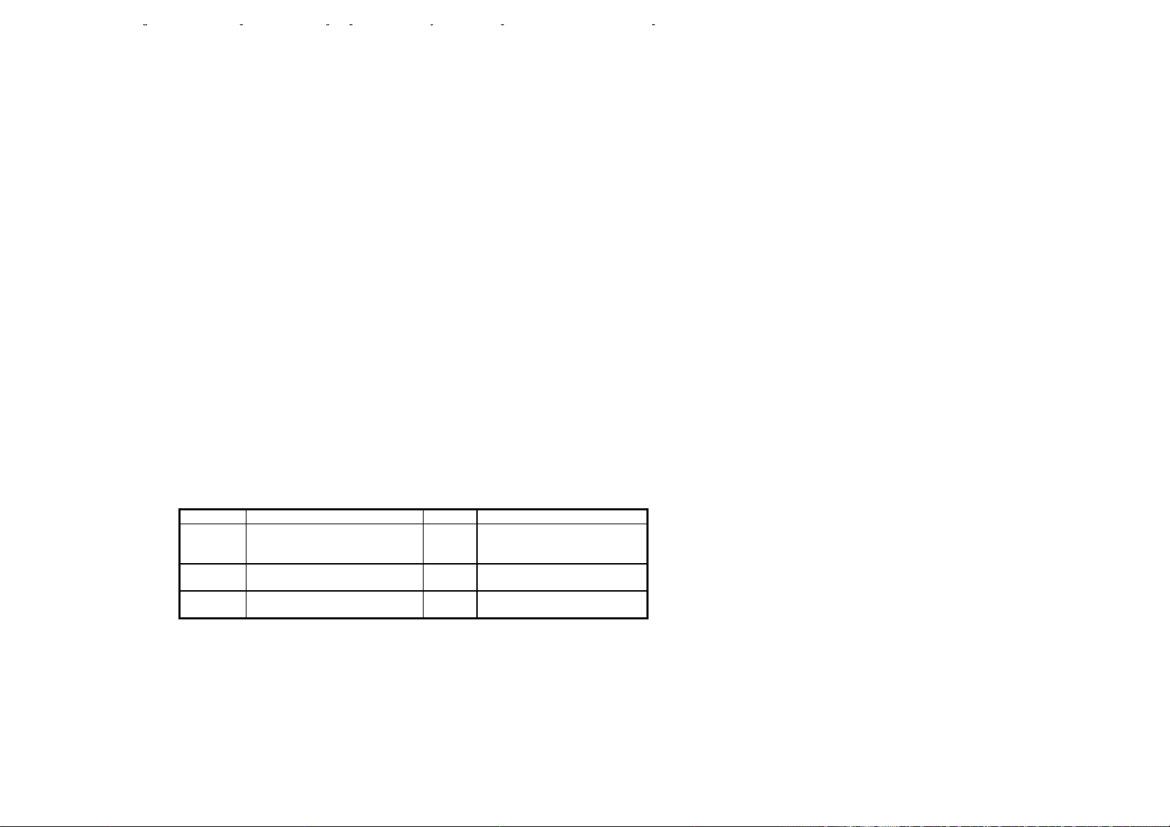
Table of Jumpers
JUMPER AREA OF INFLUENCE LINK ACTION
J1 CMOS Battery Support None
CLR
NORM
JP6 CPU and PCI bus speed plus
CPU internal speed
J21 Panel voltage supply 3V/5V 3.3V supply
Not Allowed
Clear CMOS RAM
Use on-board battery
See “
Speed Setting JP6” on page 23
5V supply
USER-INSTALLABLE UPGRADES
SYSTEM MEMORY
The table shows the possible memory combinations. ATOM will support both Fast Page DRAM or EDO
DRAM SIMMs, but they cannot be mixed. Parity/Error Correction is supported when using parity SIMMs
(x36).
Page 21
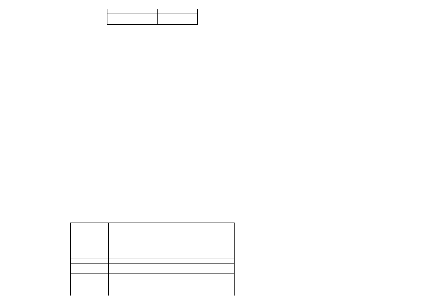
8M X 32 (32 MB) 64 MB
16M X 32 (64 MB) 128 MB
32M X 32 (128 MB) 256 MB
Note: SIMMs may be parity (x 36) or non-parity (x 32)
EDO DRAM
Extended Data Out (or Hyper Page) DRAM is designed to improve the DRAM read performance. EDO
DRAM holds the memory data valid until the next CAS# falling edge, unlike standard fast page mode
DRAM which tri-states the memory data when CAS# negates to precharge for the next cycle. With
EDO, the CAS# precharge overlaps the data valid time, allowing CAS# to negate earlier while still
satisfying the memory data valid window time.
REAL TIME CLOCK BATTERY REPLACEMENT
The on-board battery may be replaced using a Duracell DL2032 3 volt button cell, or equivalent.
GRAPHICS MEMORY UPGRADE
The C&T B69000 has 2 MB of DRAM installed for graphics. When the 69030 becomes available this will
allow 4MB of graphics to be offered.
SOLID STATE DISK SUPPORT
ATOM supports the use of Solid State Disks (SSD) using M-Systems Flash devices fitted to the board using
the DIL socket.
Please contact Blue Chip Technology’s Technical Services for details.
ADDRESS MAPS
MEMORY MAP
ADDRESS
RANGE
(DECIMAL)
1024K - 131072K 100000 - 8000000 127M Extended Memory
896K - 1023K E0000 - FFFFF 128K Phoenix System BIOS
K - K CE000 - CFFFF 8K Solid State Disk Pages
848K - 879K D4000 - DBFFF 32K BIOS Extensions
800K - K C8000 - CDFFF K Available HI DOS memory
640K - 799K A0000 - C7FFF 160K On-board video memory and
639K 9FC00 - 9FFFF 1K Extended BIOS Data
ADDRESS
RANGE
(HEX)
SIZE DESCRIPTION
(not available for UMB)
(open to ISA and PCI bus)
BIOS
(moveable by QEMM, 386MAX)
Page 22

various addresses or disabled. These I/O locations are listed in the Variable Resources column.
ADDRESS
(HEX)
0000 - 000F 16 PIIIX - DMA 1
0020 - 0021 2 PIIIX - Interrupt Controller 1
002E - 002F 2 Ultra I/O configuration registers
0040 - 0043 4 PIIIX - Timer 1
0060 1 Keyboard Controller Data Byte
0061 1 PIIIX - NMI, speaker control
0064 1 Kbd Controller, CMD/STAT Byte
0070, bit 7 1 bit PIIIX - Enable NMI
0070, bits 6:0 7 bits RTC, Address
0071 1 RTC, Data
0080 - 008F 16 PIIIX - DMA Page Register
00A0 - 00A1 2 PIIIX - Interrupt Controller 2
00B2 - 00B3 2 PIIIX - APM Control / Status
00C0 - 00DE 31 PIIIX - DMA 2
00F0 1 Reset Numeric Error
0100 - 0107 8 Reserved for Board Confign.
0170 - 0177 8
01F0 - 01F7 8 Primary IDE Channel
0200 - 0207 8 Gameport Joystick
0220 Audio
0278 - 027B 4
02E8 - 02EF 8
02F8 - 02FF 8 Serial Port 2
0376-377 2
0378 - 037F 8 Parallel Port 1
0388 Audio
03B0 - 03BB 4 C&T69000
03BC - 03BF 4
03C0 - 03DF 16 C&T69000
03E8 - 03EF 8
03F0 - 03F5 6 Floppy Channel 1
03F6 1 Pri IDE Chan Cmnd Port
03F7 (Write) 1 Floppy Chan 1 Cmd
03F7, bit 7 1 bit Floppy Disk Chg Chan 1
03F7, bits 6:0 7 bits Pri IDE Chan Status Port
03F8 - 03FF 8 Serial Port 1
LPT + 400h 3 ECP regs, LPT base +
04D0 - 04D1 2 Edge/Level INTR Control Reg.
0CF8 - 0CFC* 4 PCI Config Address Reg.
0CF9 1 Turbo & Reset control Reg.
0CFC - 0CFF 4 PCI Config Data Reg
FFA0 - FFA7 8 1ary Bus MasterIDE regs
FFA8 - FFAF 8 2ary Bus Master IDE regs
FF00-FF07 8 IDE Bus Master Reg.
SIZE
Bytes
FIXED RESOURCES VARIABLE
RESOURCES
Interrupt Controller 2
400h
*only accessible by DWORD accesses.
PCI CONFIGURATION SPACE MAP
The Triton chipset uses Configuration Mechanism 1 to access the PCI configuration space. The PCI
Page 23
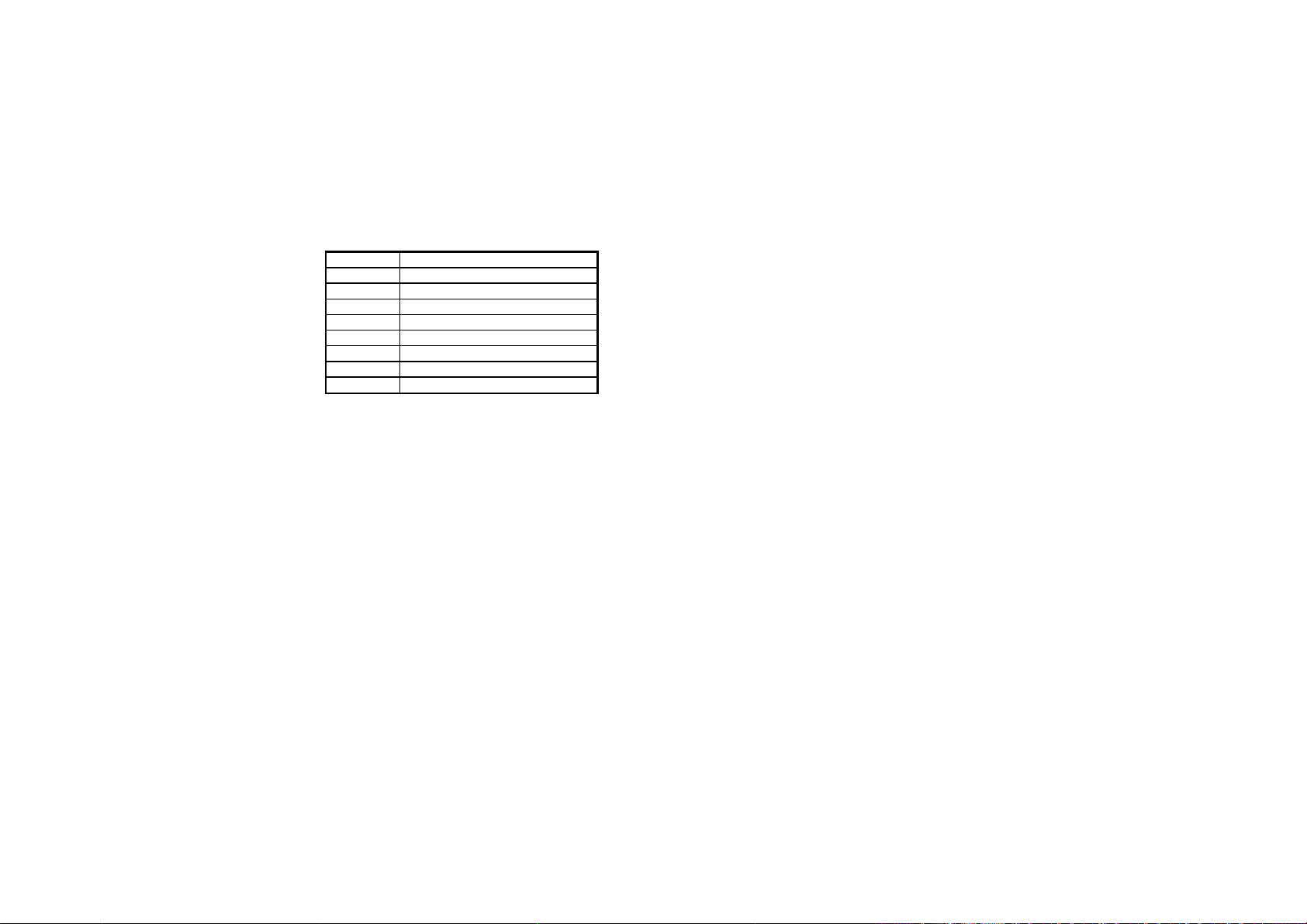
1. Using a DWORD read or write command, read or write data from the I/O port CFCH
NOTE: Any address output to CF8H is always on a 4 byte (DWORD) boundary. You can read or write
any BYTE, WORD or DWORD in the four byte range by using the correct offset as follows:
DWORD @ CFCh
WORD @ CFCh or CFEh
BYTE @ CFCh, CFDh, CFEh or CFFh
CONFIGURATION ADDRESS REGISTER BIT DEFINITION
BIT FUNCTION / SETTING
31 1
30 - 24 RESERVED
23 -16 BUS NUMBER
15 - 11 DEVICE NUMBER
10 - 8 FUNCTION NUMBER
7 - 2 REGISTER NUMBER
1 0
0 0
CONFIG SPACE ENABLE FLAG (Bit 31): Always 1 to indicate I/O access is to configuration space.
RESERVED (Bits 30-24): Always 00h
BUS NUMBER (Bits 23-16): Always 00h unless a bridge card is installed in a PCI slot
DEVICE NUMBER (Bits 15-11): Used to indicate a specific PCI device. The Triton TSC has a
predefined device number of 00000h. The PIIIX and four PCI slots also have specific device numbers,
that device number is determined by which PCI Address/Data line is connected to the device’s ID SEL
pin. Specific mapping information is detailed in the table below.
FUNCTION NUMBER (Bits 10-8): Used to indicate a specific function in multifunction PCI devices.
The PIIIX is the only multi-function device on ATOM located on the single board PC. Use 00h for the
basic PIIIX device and 01h for the PCI IDE BUS MASTER FUNCTION. For a multi-function PCI addin card, refer to the card’s documentation to determine the allowable function numbers.
REGISTER NUMBER (Bits 7-2): Defines one of 64 DWORD locations for a specific PCI device.
Note that Bits 1 and 0 must always be 0h for DWORD access.
Page 24
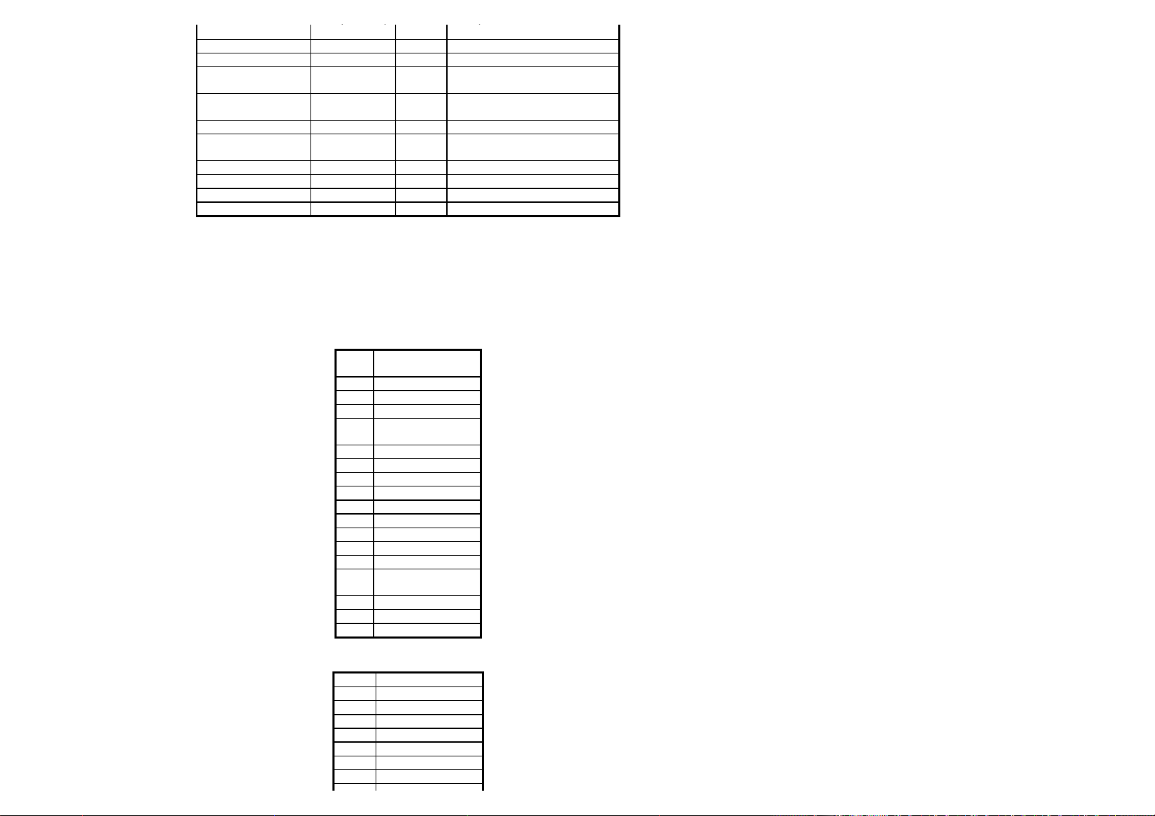
DEVICE BUS/DEVICE/
ID SEL I/O CONFIG ADDRESS
TSC 00 / 00 / 0 N/A 8000 0000 - 8000 00FC
PIIIX 00 / 07 / 0 AD18 8000 3800 - 8000 38FC
PIIIX-IDE BUS
MASTER
PIIX-Serial Bus
Controller (USB)
C&T69000 00 / 08 / 0 AD13 8000 4000 - 8000 40FC
RTL8139A
(Ethernet)
Slot 1 AD19
Slot 2 AD20
Slot 3 AD21
Slot 4 AD22
FUNCTION
00 / 07 / 1 AD18 8000 3900 - 8000 39FC
00 / 07 / 2 AD18 8000 3A00 - 8000 3AFC
00 / 09 / 0 AD14 8000 4100 - 8000 41FC
REGISTER
INTERRUPTS & DMA CHANNELS
The following tables list the Interrupt and DMA Channel configuration options for on-board devices. The
serial ports, parallel ports, and IDE controller can be configured using SETUP, or any other Plug and Play
resource manager (such as the Windows™ 95/98 Device Manager). The Graphics interrupt is assigned by
the auto-configure utility during boot up.
IRQ RESERVED
NMI I/O Channel Check
10
11 Ethernet
12 PS/2 Mouse
13 Math co-processor
14 Primary E-IDE
15
DMA RESERVED
INTERRUPTS
0 Interval Timer
1 Keyboard buffer full
2 Cascade interrupt
from slave PIC
3 Serial 2 (COM2)
4 Serial 1 (COM1)
5 Audio
6 Floppy Controller
7 Parallel (LPT1)
8 Real time clock
9 VGA if used, USB
(if present)
0 Audio*
1 Audio*
2 Floppy
3
4 Cascade channel
5
6
Page 25
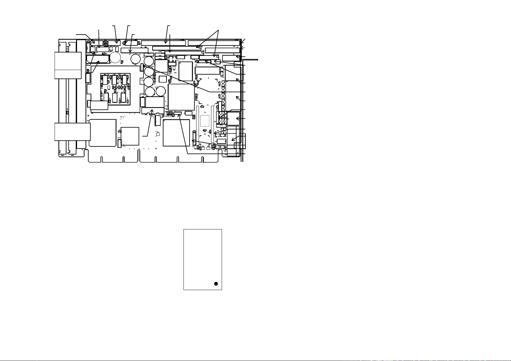
COM B
CPU
CELL
USB
FAN
POWER
POWER
SPEED
RS232
RS485/422
UTILS
FLOPPY
ZOOM VIDEO
PANEL
IDE
PRINTER
AUDIO
CD
VEE
10/100BASE T
PANEL POWER
VGA
MOUSE
KBD & MOUSE
MEMORY/
CACHE
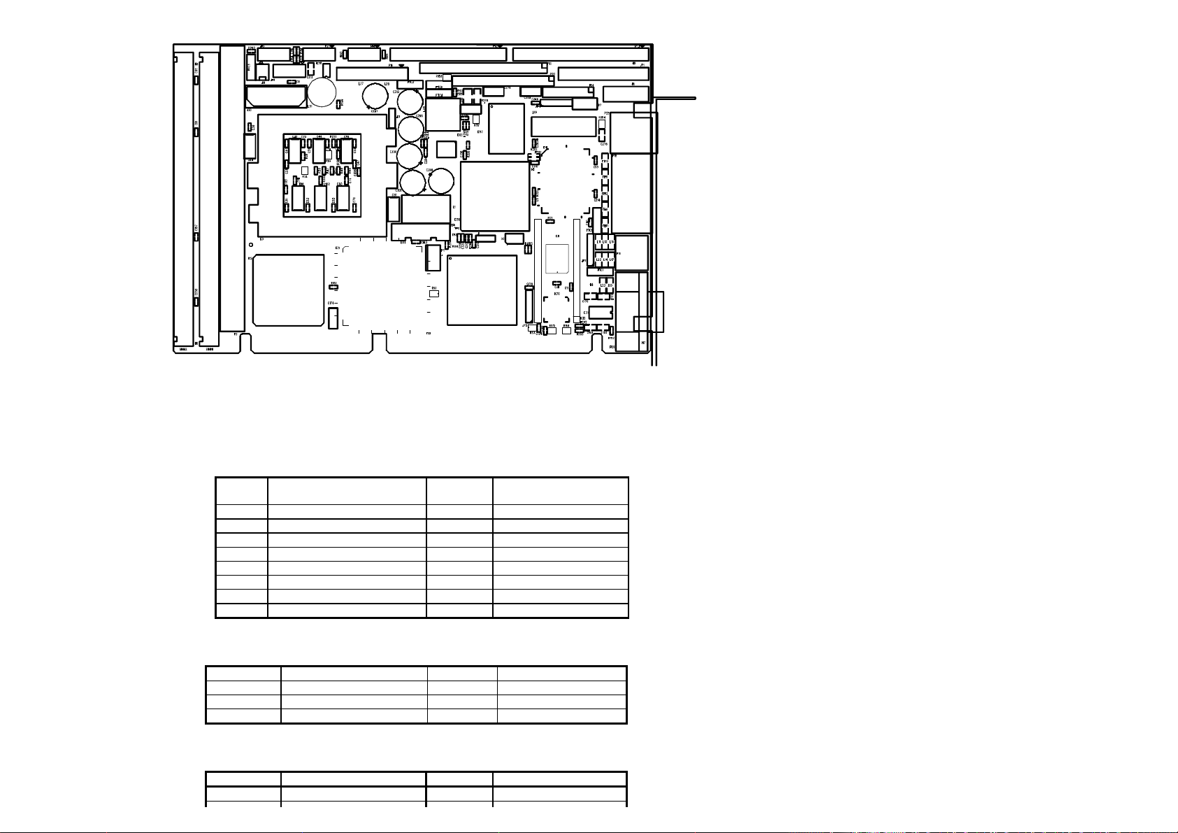
All open header pin 1 towards metal bracket =>. Square pad identifies pin 1.
PISA and ISA board versions identical except for edge fingers.
SOLID STATE DISK (SSD) ORIENTATION
Locate device as shown into above diagram.
Li
SSD
COM A
IRDA
CMOS
Page 26
BACK PANEL CONNECTORS
The back panel houses the following connectors:
VIDEO CONNECTOR P18 (15 WAY CONDENSED D-TYPE)
PIN
NO.
1 Analogue RED 2 Analogue GREEN
3 Analogue BLUE 4 Not Used
5 0 Volts (Ground) 6 0 Volts (Ground)
7 0 Volts (Ground) 8 0 Volts (Ground)
9 5V limited current 10 0 Volts (Ground)
11 Not Used 12 DCD
13 Horizontal Sync 14 Vertical Sync
15 DCC
PS/2 KEYBOARD PORT P19 (6 WAY MINI-DIN)
PIN NO. SIGNAL PIN NO. SIGNAL
1 Keyboard Data 2 Mouse Data
3 Ground 4 +5 Volts (fused)
5 Keyboard Clock 6 Mouse Clock
SIGNAL PIN NO. SIGNAL
RS232 SERIAL PORT 1 P20 (9 WAY D-TYPE)
PIN NO. SIGNAL PIN NO. SIGNAL
1 Data Carrier Detect 2 -Receive Data
Page 27
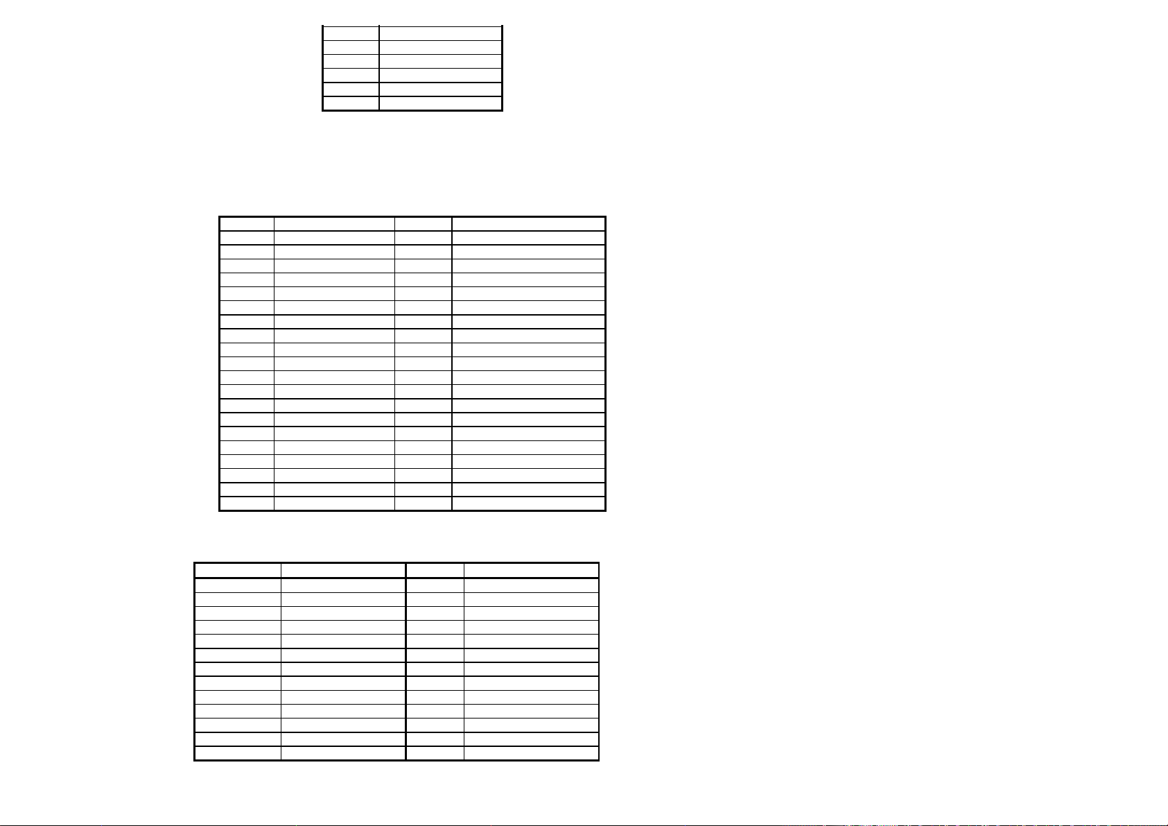
2 -VE TRANSMIT
3 +VE RECEIVE
4 NC
5 NC
6 -VE RECEIVE
7 NC
8 NC
NTERNAL I/O HEADERS & CONNECTORS
The board has a number of internal peripheral connections:
PRIMARY E-IDE CONNECTOR P13 (2X20 WAY HEADER)
PIN NO. SIGNAL PIN NO. SIGNAL
1 -Reset 2 Ground
3 Data bit 7 (HD) 4 Data bit 8 (HD)
5 Data bit 6 (HD) 6 Data bit 9 (HD)
7 Data bit 5 (HD) 8 Data bit 10 (HD)
9 Data bit 4 (HD) 10 Data bit 11 (HD)
11 Data bit 3 (HD) 12 Data bit 12 (HD)
13 Data bit 2 (HD) 14 Data bit 13 (HD)
15 Data bit 1 (HD) 16 Data bit 14 (HD)
17 Data bit 0 (HD) 18 Data bit 15 (HD)
19 Ground 20 Polarisation
21 Drive Request 22 Ground
23 -IO Write (HD) 24 Ground
25 -IO Read (HD) 26 Ground
27 Drive Ready 28 Cable select 330ohm to 0V
29 Drive Acknowledge 30 Ground
31 IRQ14 32 Not Used
33 Address 1 (HD) 34 1 Kohm to 0V
35 Address 0 (HD) 36 Address 2 (HD)
37 -Chip Select 0 (HD) 38 -Chip Select 1 (HD)
39 IDE LED Drive 40 Ground
ECP/EPP PARALLEL PORT JP1 (2X13 WAY HEADER)
PIN N°°
1 -Strobe 2 -Auto Feed XT
3 Data bit 0 4 -Error
5 Data bit 1 6 -Initialise
7 Data bit 2 8 -Select (input)
9 Data bit 3 10 Ground
11 Data bit 4 12 Ground
13 Data bit 5 14 Ground
15 Data bit 6 16 Ground
17 Data bit 7 18 Ground
19 -Acknowledge 20 Ground
21 Busy 22 Ground
23 Paper Empty 24 Ground
25 Select (Output) 26 Polarisation
SIGNAL
PIN N°°
SIGNAL
Page 28
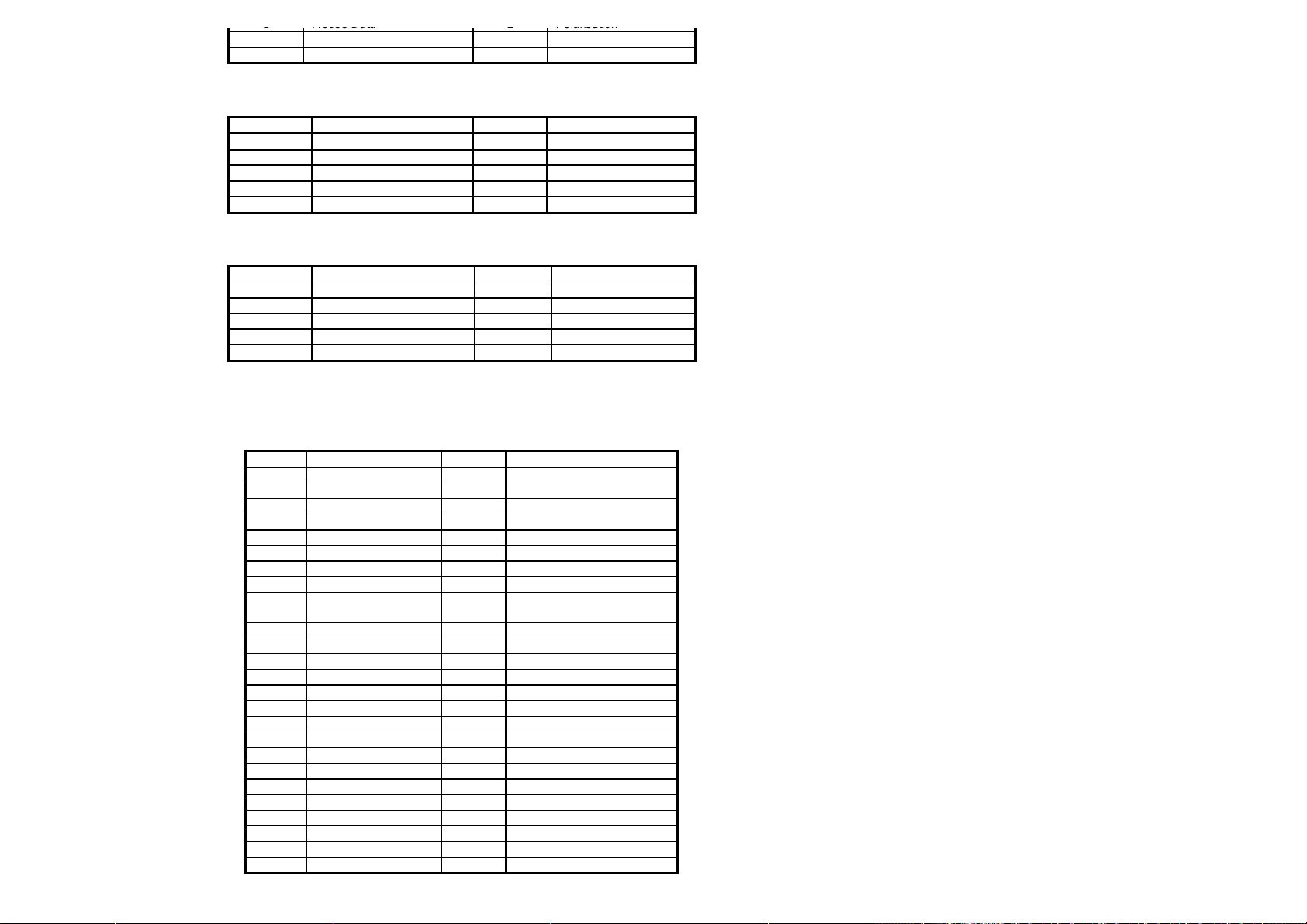
1 Mouse Data 2 Polarisation
3 Ground 4 +5 Volts (fused)
5 Mouse Clock
RS232 SERIAL PORT 2 P21 (2X5 WAY HEADER)
PIN NO. SIGNAL PIN NO. SIGNAL
1 -Data Carrier Detect 2 -Receive Data
3 -Transmit Data 4 -Data Terminal Ready
5 Ground 6 -Data Set Ready
7 -Ready To Send 8 -Clear To Send
9 -RI 10 Polarisation
DUAL USB PORTS JP3 (2X5 WAY HEADER)
PIN NO. SIGNAL PIN NO. SIGNAL
1 USB VCC0 2 Ground
3 USB DATA0- 4 USB Ground1
5 USB DATA0+ 6 DATA1+
7 USB Ground0 8 DATA19 Ground 10 USB VCC1
LCD PRIMARY CONNECTOR P11 (2X25 WAY 2MM HEADER)
PIN NO. SIGNAL PIN NO. SIGNAL
1 3.3v or 5v as selected 2 Vertical Sync
3 Switched +12 volts 4 Ground
5 Switched VEE 6 Horizontal Sync
7 Switched +5 volts 8 Ground
9 Switched +5 volts 10 General Purpose 1
11 Shift Clock 12 Ground
13 Line Clock 14 General Purpose 0
15 MOD 16 Ground
17 FLM (LCD equivalent
of VSYNC)
19 Panel Data 0 20 Ground
21 Panel Data 1 22 Panel Data 23
23 Panel Data 2 24 Ground
25 Panel Data 3 26 Panel Data 22
27 Panel Data 4 28 Ground
29 Panel Data 5 30 Panel Data 21
31 Panel Data 6 32 Ground
33 Panel Data 7 34 Panel Data 20
35 Panel Data 8 36 Ground
37 Panel Data 9 38 Panel Data 19
39 Panel Data 10 40 Ground
41 Panel Data 11 42 Panel Data 18
43 Panel Data 12 44 Ground
45 Panel Data 13 46 Panel Data 17
47 Panel Data 14 48 Ground
49 Panel Data 15 50 Panel Data 16
18 Ground
Page 29
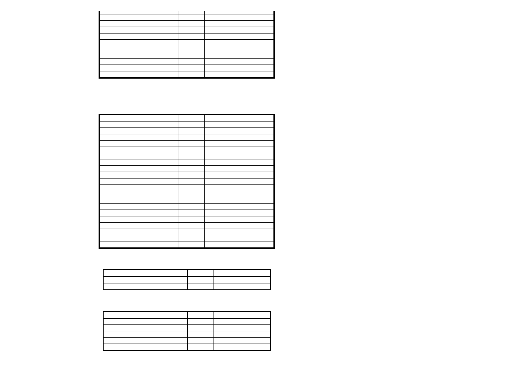
PIN NO. SIGNAL PIN NO. SIGNAL
1 Ground 2 Panel Data 35
3 Panel Data 24 4 Ground
5 Panel Data 25 6 Panel Data 34
7 Ground 8 Panel Data 33
9 Panel Data 26 10 Ground
11 Panel Data 27 12 Panel Data 32
13 Ground 14 Panel Data 31
15 Panel Data 28 16 Ground
17 Panel Data 29 18 Panel Data 30
19 Ground 20 Ground
DIGITAL VIDEO OPTION P23 (2X20 WAY 2MM HEADER)
PIN NO. SIGNAL PIN NO. SIGNAL
1 Ground 2 VP0
3 Ground 4 VP1
5 Ground 6 VP2
7 Ground 8 VP3
9 Ground 10 VP4
11 Ground 12 VP5
13 Ground 14 VP6
15 Ground 16 VP7
17 Ground 18 VP8
19 Ground 20 VP9
21 Ground 22 VP10
23 Ground 24 VP11
25 Ground 26 VP12
27 Ground 28 VP13
29 Ground 30 VP14
31 Ground 32 VP15
33 Ground 34 HREF
35 Ground 36 VREF
37 Ground 38 VRDY
39 Ground 40 Ground
CD-AUDIO INPUT P7 (4 WAY BOX SOCKET)
Pin N°°
1 CD Audio In Left 2 Audio Ground
3 CD Audio In Right 4 Audio Ground
Signal
Pin N°°
AUDIO CONNECTOR P8 (2X5 WAY 2MM BOX SOCKET)
Pin N°°
1 Line In Left 2 Line In Right
3 Audio Ground 4 Audio Ground
5 Microphone In 6 Not Used
7 Audio Ground 8 Audio Ground
9 Line Out Left 10 Line Out Right
Signal
Pin N°°
Signal
Signal
Page 30
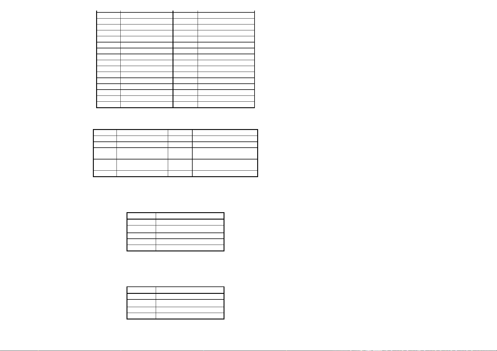
1 Ground 2 Densel
3 Ground 4 Polarisation
5 Ground 6 Rate
7 Ground 8 -Index
9 Ground 10 -Motor 0
11 Ground 12 -Drive select 1
13 Ground 14 -Drive select 0
15 Ground 16 -Motor 1
17 Ground 18 +Direction
19 Ground 20 -Step
21 Ground 22 -Write Data
23 Ground 24 -Write Gate
25 Ground 26 -Track 0
27 Ground 28 -Write Protect
29 Ground 30 -Read Data
31 Ground 32 +Head Select
33 Ground 34 +Disk Change
RS485 SERIAL PORT 2 P14 (2X5 WAY HEADER)
PIN NO. SIGNAL PIN NO. SIGNAL
1 +Rx FDX 2 +Term. 10 K to +5V
3 -Rx FDX 4 No Connect
5 +Tx FDX,
+Rx/+Tx HDX
7 -Tx FDX,
-RX/-Tx HDX
9 -Term. 10 K to Gnd 10 No Connect
6 No Connect
8 Polarisation
IRDA CONNECTOR JP5 (5 WAY HEADER)
Pin N°°
1 VCC
2
3 RRX
4 Ground
5 RTX
Polarisation
Signal
BATTERY CONNECTOR P1 (4 WAY HEADER)
Pin N°°
1 +3.6 Volts DC
2
3 Ground
4 Ground
Polarisation
Signal
FAN POWER CONNECTOR J19 (2 WAY HEADER)
Page 31
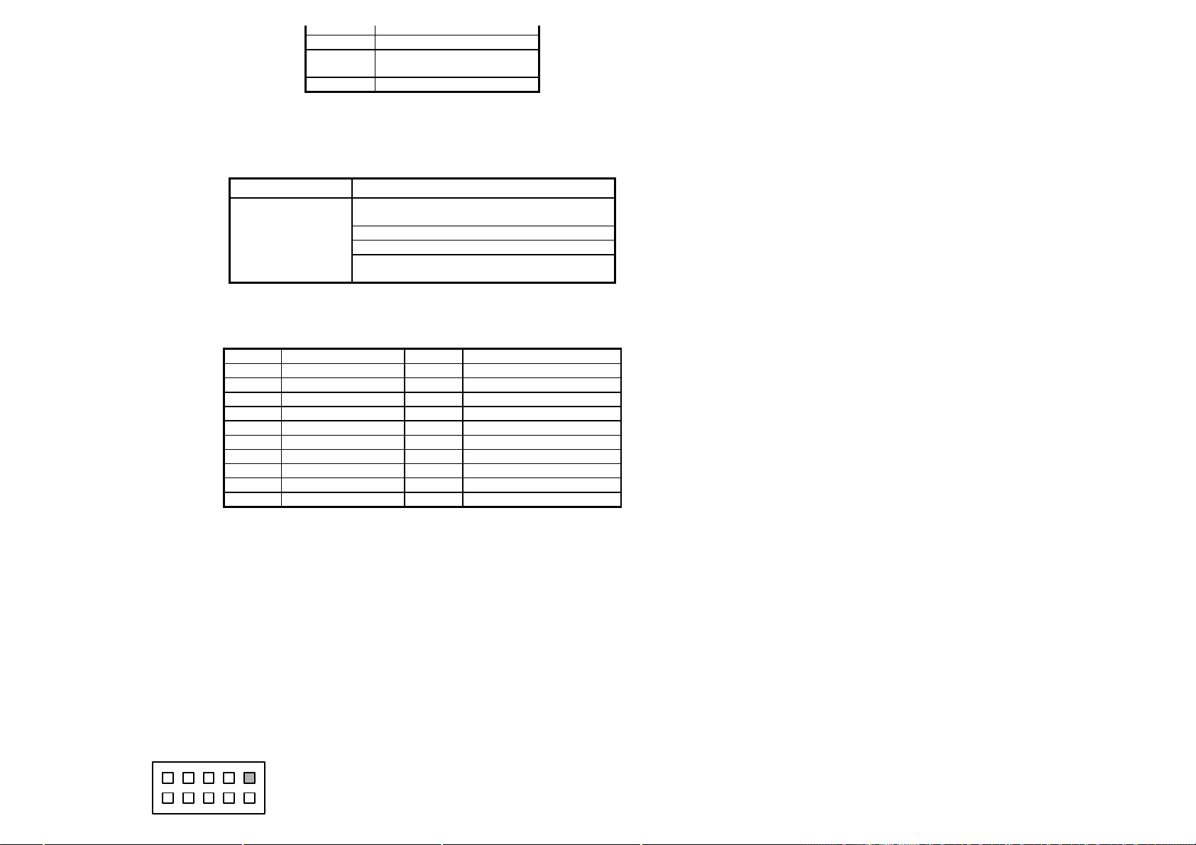
2
Polarisation
3 Enable VEE
4 Switched VEE (to LCD
5 Ground
POWER CONNECTOR J20 (4 WAY)
connector)
Pin N°
Standard 5.25” Disk
Drive Connector
+5 Volts DC
0 Volts
0 Volts
+12 Volts DC (Only required for Ethernet and
audio).
Signal
UTILITY CONNECTOR P16 (2X10 WAY HEADER)
PIN N°°
1 Speaker +ve 2 Speaker -ve
3 Reset +ve 4 Reset -ve (Ground)
5 NU 6 NU
7 Keylock +ve 8 Keylock -ve (Ground)
9 Power LED +ve 10 Power LED -ve (Ground)
11 External SMI +ve 12 External SMI -ve (Ground)
13 IDE LED +ve 14 IDE LED -ve
15 +5V limited current 16 0 Volts (Ground)
17 External Battery 18 0 Volts Battery (Ground)
19 Keyboard Data 20 Keyboard Clock
SIGNAL
PIN N°°
SIGNAL
COAST CACHE CONNECTOR P3
This is an industry-standard connector for Cache On A Stick. The COAST connector is a 160-pin
socket which is designed to prevent reversed fitting of the cache module.
Please note that each cache module is designed specifically for each chipset i.e. there are cache modules
specific to the 430HX Triton chipset. The available options for ATOM cache are 256kbyte
asynchronous, 256 or 512KByte of synchronous Pipeline burst, or none.
SPEED SETTING JP6
BF2 1 0 F1 0
Pin 1
0 = Jumper present
1 = Jumper absent
Page 32
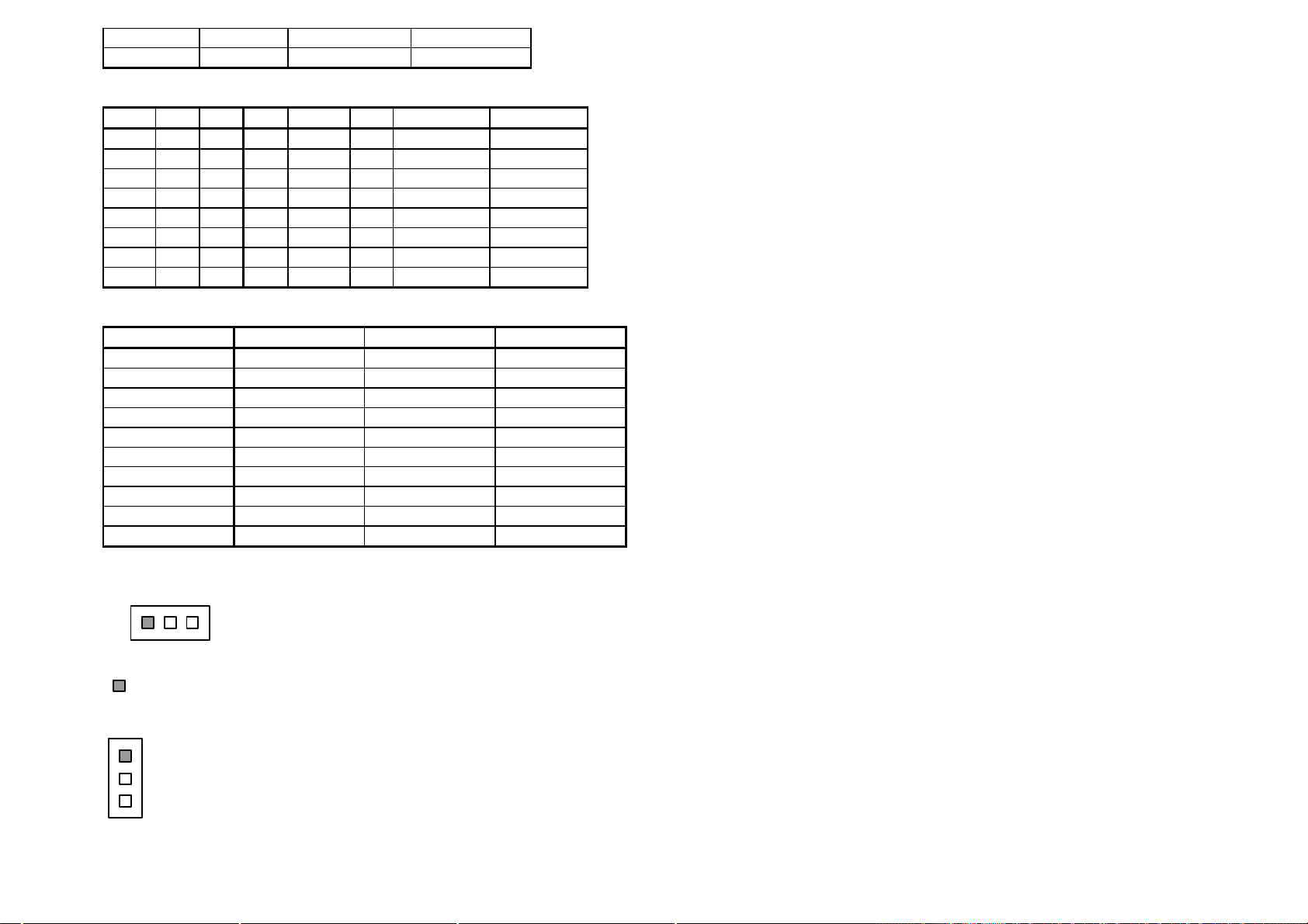
0 1 66MHz 33MHz
1 1 Not allowed -
Common Processor multiplier jumper settings
BF2 BF1 BF0 P MMX C6 K6(-2)[0:7] K6(-2)[F:8]
0 0 0 - 4.5 4.5
0 0 1 5 5 5
0 1 0 4 4 4
0 1 1 - 5.5 5.5
1 0 0 2.5 2.5 - 2.5 2.5
1 0 1 3 3 3 3 3
1 1 0 2 2 2 2 6
1 1 1 1.5 3.5 4 3.5 3.5
Internal CPU speed from Host Bus Speed
Multiplier 50MHz 60MHz 66MHz
1.5 75 90 100
2 100 120 133
2.5 125 150 166
3 150 180 200
3.5 175 210 233
4 200 240 266
4.5 225 270 300
5 250 300 333
5.5 275 330 366
6 300 360 400
CMOS CLEAR J1
Normal Clear
= Pin 1
PANEL SUPPLY J21
5V
3.3V
J1/J21: Link two pins as appropriate without power applied. Orientations as in diagrams of board outline p17.
BUS Connectors
Page 33
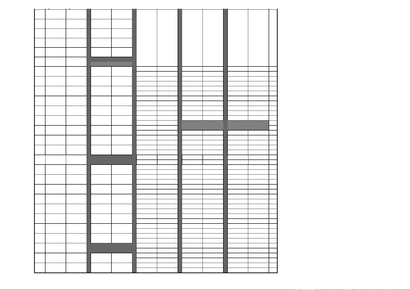
num. up row up row low row low row side B side A side B side A side B side A
1 /IOCHCHK GND
I2CLK I2DAT
2 SD7 RSTDRV
GND GND
3 SD6 Vcc
INTB# INTA#
4 SD5 IRQ9
INTD# INTC#
5 SD4 -5V
Vcc Vcc
6 SD3 DRQ2
7 SD2 -12V -12V TRST# -12V TRST# -12V TRST# 1
Vcc V I/O TCK +12V TCK +12V TCK +12V 2
8 SD1 /0WS GND TMS GND TMS GND TMS 3
PCIRST# PCICLK2 TDO TDI TDO TDI TDO TDI 4
9 SD0 +12V VCC VCC VCC VCC VCC VCC 5
GNT#0 GND VCC INTA# VCC INTA# VCC INTA# 6
10 IOCHRDY GND INTB# INTC# INTB# INTC# INTB# INTC# 7
REQ#0 GNT#1 INTD# VCC INTD# VCC INTD# VCC 8
11 AEN /SMEMW PRSNT1# PRSNT1# PRSNT1# 9
GND GND VCC V I/O 3.3V 10
12 SA19 /SMEMR PRSNT2# PRSNT2# PRSNT2# 11
PCICLK1 REQ#1 GND GND 12
13 SA18 /IOW GND GND 13
GND AD31 14
14 SA17 /IOR GND RST# GND RST# GND RST# 15
AD30 AD29 CLK VCC CLK V I/O CLK 3.3V 16
15 SA16 /DACK3 GND GNT# GND GNT# GND GNT# 17
REQ#2 PCICLK3 REQ# GND REQ# GND REQ# GND 18
16 SA15 DRQ3 VCC V I/O 3.3V 19
AD31 AD30 AD31 AD30 AD31 AD30 20
17 SA14 /DACK1 AD29 3.3V AD29 3.3V AD29 3.3V 21
GNT#2 PCICLK4 GND AD28 GND AD28 GND AD28 22
18 SA13 DRQ1 AD27 AD26 AD27 AD26 AD27 AD26 23
AD28 AD27 AD25 GND AD25 GND AD25 GND 24
19 SA12 /RFRSH 3.3V AD24 3.3V AD24 3.3V AD24 25
AD26 AD25 C/BE3# IDSEL C/BE3# IDSEL C/BE3# IDSEL 26
20 SA11 SYSCLK AD23 3.3V AD23 3.3V AD23 3.3V 27
AD24 CBE#3 GND AD22 GND AD22 GND AD22 28
21 SA10 IRQ7 AD21 AD20 AD21 AD20 AD21 AD20 29
AD22 AD23 AD19 GND AD19 GND AD19 GND 30
22 SA9 IRQ6 3.3V AD18 3.3V AD18 3.3V AD18 31
AD20 AD21 AD17 AD16 AD17 AD16 AD17 AD16 32
23 SA8 IRQ5 C/BE2# 3.3V C/BE2# 3.3V C/BE2# 3.3V 33
AD18 AD19 GND FRAME# GND FRAME# GND FRAME# 34
24 SA7 IRQ4 IRDY# GND IRDY# GND IRDY# GND 35
PWRGDIN REQ#3 3.3V TRDY# 3.3V TRDY# 3.3V TRDY# 36
25 SA6 IRQ3 DEVSEL# GND DEVSEL# GND DEVSEL# GND 37
GND STOP# GND STOP# GND STOP# 38
26 SA5 /DACK2 LOCK# 3.3V LOCK# 3.3V LOCK# 3.3V 39
GND GNT#3 PERR# SDONE PERR# SDONE PERR# SDONE 40
27 SA4 T/C 3.3V SBO# 3.3V SBO# 3.3V SBO# 41
AD16 AD17 SERR# GND SERR# GND SERR# GND 42
Page 34
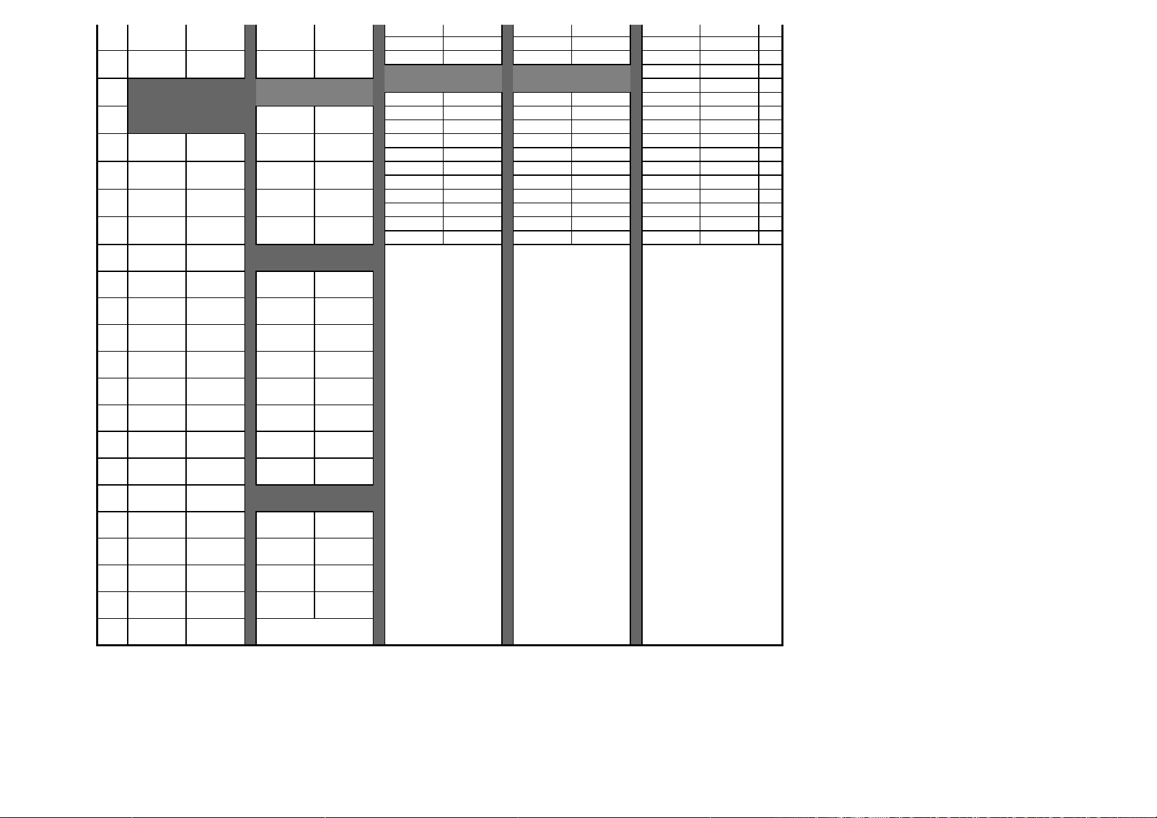
30 SA1 OSC AD12 AD11 AD12 AD11 AD12 AD11 47
31 SA0 GND GND AD09 GND AD09 M66EN AD09 49
TRDY# LOCK# AD10 GND AD10 GND AD10 GND 48
STOP# PERR# GND GND 50
32 GND GND 51
AD08 C/BE0# AD08 C/BE0# AD08 C/BE0# 52
33 AD07 3.3V AD07 3.3V AD07 3.3V 53
GND SERR# 3.3V AD06 3.3V AD06 3.3V AD06 54
34 AD05 AD04 AD05 AD04 AD05 AD04 55
AD15 AD03 GND AD03 GND AD03 GND 56
35 /SBHE /MCS16 GND AD02 GND AD02 GND AD02 57
CBE#1 AD14 AD01 AD00 AD01 AD00 AD01 AD00 58
36 LA23 /IOCS16 VCC VCC V I/O V I/O VCC VCC 59
PAR AD12 ACK64# REQ64# ACK64# REQ64# ACK64# REQ64# 60
37 LA22 IRQ10 VCC VCC VCC VCC VCC VCC 61
GND GND VCC VCC VCC VCC VCC VCC 62
38 LA21 IRQ11
39 LA20 IRQ12
40 LA19 IRQ15
41 LA18 IRQ14
42 LA17 /DACK0
43 /MEMR DRQ0
44 /MEMW /DACK5
45 S D8 DRQ5
46 SD9 /DACK6
47 SD10 DRQ6
48 SD11 /DACK7
49 SD12 DRQ7
50 SD13 Vcc
51 SD14 /MASTER
52 SD15 GND
GND M66EN
AD13 AD10
AD11 AD8
AD9 AD7
CBE#0 AD5
AD6 AD3
AD4 AD1
AD2 AD0
Vcc V I/O
Vcc Vcc
GND GND
GND GND
Page 35

ATOM USER MANUAL ERROR MESSAGES PAGE 27
ERROR MESSAGES
ERROR BEEP CODES
The BIOS performs a Power On Self Test (POST) after a reset or reboot. If errors occur during the POST,
the microprocessor indicates the status of the test by writing codes to the I/O port at address 80 Hex.
Some of the fatal errors produce audible codes which indicate the source of the problem. For a list of these
refer to the BIOS user manual.
BLUE CHIP TECHNOLOGY LTD. 01271029.DOC PAGE 27
 Loading...