

Page 1

APEX II
Single Board Computer
(SBC)
User Manual
Page 2

APEX II
User Manual
Document Part N° 127-171
Document Reference APEXII\..\127-171.doc
Document Issue Level 3.1
Manual covers PCBs with the following Issue N° 3.x (x is any digit)
All rights reserved. N o part of this publica tion may be r eproduced, stored in any retrieval system, or
transmitted, in any form or by any means, electronic, mechanica l, photocopied, recorded or other wise,
without the pri or permi ssion, in wr iti ng, from t he pu bl isher . For permi ssion in the UK conta ct B l u e C hip
Technology.
Information offered in this ma nual i s correct at the time of printing. Blue Ch ip Technology a ccepts no
responsibility for any inaccuracies. This information is subject to change without notice.
All trademarks and registered names acknowledged.
Blue Chip Technology Ltd.,
Chowley Oak, Tattenhall,
Chester, Cheshire,
CH3 9EX
Telephone : 01829 772000 Facsimile : 01829 772001
Page 3

Amendment History
Issue
Level
1.0 12/07/95 DS First Issue
2.0 14/12/95 BH CPU fitment, EMC statement & version 1.5 LCD tables
3.0 07/06/96 EGW Revised for PCB Issue 3.x. 386 option removed. 3v3
3.1 22/04/97 EGW List of supported CPUs updated. Document Issue level
Issue
Date
Author Amendment Details
included
option added. Clock synth options added. -5 & -12 V
connectios added. Contents re-instated. Bus Connector
table errors corrected. List of supported CPUs updated.
Ext battery voltage was 3.6 V.
raised to 3.1
Page 4

CONTENTS
1. INTRODUCTION .......................................................................................1
1.1 M
ANUAL OBJECTIVES
1.2 L
IMITATIONS OF LIABILITY
1.3 CMOS S
1.4 O
1.5 R
ELATED PUBLICATIONS
1.6 T
RADEMARKS
TATIC DISCHARGES
N-BOARD BATTERY
...............................................................................................3
...................................................................................1
............................................................................2
.........................................................................2
....................................................................................2
...............................................................................3
2. THE APEX II PRODUCT RANGE............................................................5
2.1 G
ENERAL OVERVIEW
2.2 APEX II S
2.3 P
OWER REQUIREMENTS
2.4 PC/104 S
2.5 S
TANDARD
UPPORT MODULES
PECIFICATION
PC AT I/O
....................................................................................5
...............................................................................6
.................................................................................7
..........................................................................7
.......................................................................8
CARDS
3. USER GUIDE..............................................................................................9
3.1 I
NTRODUCTION
3.2 G
ETTING STARTED
3.3 C
ONNECTING TO THE
3.4 A
DDING MEMORY
3.5 F
INAL WIRING CHECKS
3.6 C
ONNECTING THE POWER AND SWITCHING ON
.............................................................................................9
.....................................................................................10
I/O
HEADERS
..............................................................15
.......................................................................................31
................................................................................35
..............................................36
4. TROUBLESHOOTING GUIDE............................................................... 37
4.1 I
NTRODUCTION
4.2 P
OWER SUPPLY PROBLEMS
4.3 BIOS S
4.4 CRT S
4.5 F
4.6 K
4.7 M
4.8 F
4.9 IDE H
4.10 S
4.11 P
4.12 D
TART UP PROBLEMS
CREEN PROBLEMS
LAT PANEL DISPLAY PROBLEMS
EYBOARD AND MOUSE PROBLEMS
EMORY PROBLEMS
LOPPY DISK DRIVE PROBLEMS
ARD DISK PROBLEMS
ERIAL PROBLEMS
ARALLEL PROBLEMS
IGITAL
4.13 PC/104
4.14 U
SING THE
...........................................................................................37
..........................................................................37
.........................................................................38
.............................................................................39
.................................................................40
.............................................................40
...................................................................................40
...................................................................41
.........................................................................42
....................................................................................42
................................................................................43
I/O P
ROBLEMS
PC XT/AT C
AND
APEX II
............................................................................43
ARD PROBLEMS
UNIT WITH A HOST
.................................................43
PC ............................................... 44
Page 5

5. HARDWARE TECHNICAL SECTION...................................................46
5.1 I
NTRODUCTION
5.2 APEX II ISA
5.3 IEEE P996 S
5.4 V
IDEO OUTPUTS
5.5 S
ERIAL PORTS
5.6 P
ARALLEL PORT (PRINTER PORT
5.7 24 C
5.8 D
5.9 B
5.10 P
5.11 P
HANNEL DIGITAL PROGRAMMABLE
ISK DRIVES
ATTERY (INTERNAL AND EXTERNAL
OWER SUPPLY INPUTS
ERIPHERAL (UTILITIES
5.12 POST (P
5.13 P
ASSIVE BACKPLANE DRIVING
5.14 W
ATCHDOG AND RESET CONTROL
5.15 E²PROM A
5.16 M
EMORY MAPS
5.17 I/O A
DDRESS MAP
5.18 DMA C
5.19 I
NTERRUPTS
5.20 P
HYSICAL AND ENVIRONMENTAL CONSIDERATIONS
5.21 U
NIT RELIABILITY
5.22 A
DDING MEMORY
5.23 U
SING
...........................................................................................46
PC/104 B
AND
PECIFICATION INFORMATION
US SIGNAL DESCRIPTIONS
...................................................51
................................46
.........................................................................................51
RS232
RS485 ...............................................................60
AND
) ................................................................ 61
I/O.................................................62
...............................................................................................62
).........................................................65
..............................................................................65
) C
ONNECTOR ITEMS
OWER ON SELF TEST
) I
NFORMATION
.............................................66
............................................68
...................................................................69
.............................................................70
CCESS AND CONTROL
..............................................................71
.........................................................................................72
....................................................................................72
HANNELS
......................................................................................72
..............................................................................................72
....................................72
.....................................................................................73
.....................................................................................74
APEX II
WITH A HOST
PC..............................................................77
6. SOFTWARE TECHNICAL SECTION....................................................80
6.1 I
NTRODUCTION
6.2 BIOS O
6.3 AMI W
IN
6.4 AMI BIOS M
6.5 SET-UP S
6.6 A
DVANCED
6.7 A
DVANCED CHIPSET SET-UP
6.8 P
ERIPHERAL SET-UP
6.9 U
TILITIES SET-UP SCREEN
6.10 S
ECURITY SET-UP SCREEN
6.11 D
EFAULT
6.12 S
AVING AND EXITING THE
...........................................................................................80
VERVIEWS
BIOS S
AIN SET-UP SCREEN
ECTION
(CMOS) SET-UP.......................................................................88
BIOS SET-
6.13 APEX II BIOS E
6.14 E²PROM C
6.15 M
EMORY MAPS
ONTROL
.......................................................................................80
YSTEM
BIOS U
SER FEATURES
...........................................83
...............................................................86
.......................................................................................87
........................................................................95
....................................................................................99
.........................................................................105
.......................................................................106
UP SCREEN
..............................................................107
AMI BIOS......................................................108
XTENSIONS
...................................................................108
................................................................................114
.......................................................................................114
Page 6

6.16 I/O A
6.17 DMA C
6.18 I
6.19 APEX II S
DDRESS MAP
HANNELS
NTERRUPTS ASSIGNMENTS
OFTWARE UTILITIES
..................................................................................114
....................................................................................115
.....................................................................115
................................................................115
7. APPENDIX A : CONNECTOR PINOUTS.............................................117
8. APPENDIX B : PCB LAYOUT DIAGRAM .........................................126
9. APPENDIX C : CONFIGURATION JUMPERS .................................. 127
10. APPENDIX D : INTERRUPT ASSIGNMENTS...................................128
11. APPENDIX E : DMA ASSIGNMENTS................................................129
12. APPENDIX F : I/O ASSIGNMENTS.................................................... 130
13. APPENDIX G : POWER ON SELF TEST........................................... 131
13.1 POST E
13.2 POST E
RROR BEEP CODES
RROR CODES AT THE
......................................................................131
POST
HEADER
............................................132
14. APPENDIX H : USING THE DIGITAL PI/O...................................... 137
14.1 I
NTRODUCTION
14.2 E
LECTRICAL OPTIONS
14.3 D
IGITAL
14.4 APEX II
14.5 P
ROGRAMMING GUIDE
14.6 E
XAMPLE PROGRAM
14.7 A
PPLICATION NOTES FOR INTERFACING TO THE
.......................................................................................137
.............................................................................137
I/O C
ONNECTOR PIN DETAILS
ADDRESS PORTS FOR THE
(P9) ...........................................138
71055 (8255)...................................138
...........................................................................140
................................................................................141
71055 I/O P
ORT
..............143
15. APPENDIX I : FLASH PROGRAMMING..........................................145
15.1 I
NTRODUCTION
15.2 R
EMOTE DISK CONNECTION AND OPERATION
15.3 D
EVELOPMENT KIT PROGRAMMING
15.4 R
EAD/WRITEABLE DISK DRIVE
15.5 R
EMOTE SERIAL LINK PROGRAMMING WITH KEYBOARD
15.6 R
EMOTE SERIAL LINK PROGRAMMING WITHOUT KEYBOARD OR DISPLAY
15.7 C
REATING A BOOTABLE FLOPPY DISK FOR FLASH PROGRAMMING
.......................................................................................145
...........................................146
.........................................................149
................................................................152
& D
ISPLAY
.........154
.. 162
. ............ 163
Page 7

16. APPENDIX J : SOFTWARE UTILITIES DISKS................................165
16.1 I
NTRODUCTION
16.2 APEX II S
16.3 APEX II S
.......................................................................................165
OFTWARE UTILITIES DISK
CREEN DRIVERS
......................................................................166
........................................................166
17. APPENDIX K : PERIPHERAL HARDWARE.....................................167
17.1 I
NTRODUCTION
.......................................................................................167
18. APPENDIX L : DOCUMENTATION AND TECHNICAL SUPPORT170
18.1 T
ECHNICAL DOCUMENTATION
18.2 R
EADERS COMMENTS
18.3 T
ECHNICAL SUPPORT
18.4 C
OPYING BLUE CHIP TECHNOLOGY SOFTWARE
18.5 C
USTOMER SERVICE
18.6 F
AULTY PRODUCTS
18.7 F
AULTY PRODUCT RETURNS PROCEDURE
..............................................................................170
..............................................................................171
................................................................................172
.................................................................................172
.................................................................170
.........................................172
.................................................173
19. APPENDIX M : FLAT PANEL INTERFACE CONNECTION GUIDE174
19.1 I
NTRODUCTION
19.2 P
ANEL CLASS DEFINITIONS
19.3 P
ANEL JUMPER SELECTION
19.4 LCD P
19.5 F
OWER SEQUENCING AND
LAT PANEL INTERFACE TABLES
.......................................................................................174
......................................................................175
......................................................................175
BIAS
GENERATION
..................................176
..............................................................176
20. APPENDIX N : APEX II MEMORY MAP ..........................................192
21. APPENDIX O : ELECTROMAGNETIC COMPATIBILITY.............193
22. APPENDIX P : APEX II SUPPORTED CPUS.....................................195
Page 8

Company Profile
Blue Chip Technology is the leading specialist PC product manufacturer in
UK/Europe.
Blue Chip Technology provides innovation with quality design and
manufacturing from a single source.
Based in the North West, our purpose built complex contains one of the most
advanced research and development facility, engineering workshop and
production lines.
Specialising in the provision of industrial computing and electronic solutions for
a wide range of UK and European organisations, Blue Chip Technology has one
of the UK's largest portfolios of industrial PCs, peripherals and data acquisition
cards. This extensive range of products, coupled with our experience and
expertise, enables Blue Chip Technology to offer an industrial processing
solution for any application. APEX II is the latest addition to our portfolio,
providing a cost effective product development and volume production tool for
OEMs.
A unique customisation and specialised system integration service is also
available, delivering innovative solutions to customers problems. The company's
success and reputation in this area has led to a number of large design and
manufacturing projects for companies such as BNFL, Aston Martin, Jaguar
Sport and British Gas.
British Standards Institute approval (BS EN ISO 9001) means that all of Blue
Chip Technology's design and manufacturing procedures are strictly controlled,
ensuring the highest levels of quality, reliability and performance.
Blue Chip Technology also continue to invest in the latest technology and skills
to provide high performance computer and electronic solutions for a worldwide
customer base.
Blue Chip Technology would like to thank you for purchasing this product and
we hope the APEX II enables you to prosper in the future.
Page 9

Preface
The PC as an Embedded Control Solution
As today's OEMs battle to develop leading edge products as fast as possible and
with minimal cost, the APEX II SBC provides a innovative solution. Designed to
provide a high performance, compact hardware solution, with maximum
configuration, compatibility and flexibility, APEX II is a complete PC on a
single card. This allows OEMs to incorporate PC microprocessor control into a
wide range of products with ease.
Traditional methods of embedding computer control into products are being
challenged by the latest developments in embedded PC technology. This has
resulted in a dramatic increase in the number of applications which are using
the PC as an embedded control solution.
Until recently, the only options were expensive and bulky bus board products
such as VME or STE or the resource hungry solution of designing a micro
controller from scratch. By using the APEX II processor as a "drop-in"
alternative, OEMs can gain clear cut advantages in design, production and
product enhancement.
The following examples show why :
• The PC is the best understood hardware interface in the world
• The APEX II is a complete sub-system, so design is minimised
• Resource can be focused on the application specific features of the target
product
• Development resource is reduced, saving time and money
• PC application software enhances product functionality
• User familiarity with DOS and Windows interfaces enhances product
attractiveness
• Low cost and well understood development tools reduce personnel learning
curves
• An off-the-shelf solution reduces material needs and costs
• Reduced time to market maximises sales and optimises profit
Page 10

The PC has become the control solution for many current applications, some of
these include :
• Food and Drink Processing
• Water/Gas/Oil and Electricity control
• Retailing (EPOS etc.)
• Marine
• Medical Equipment
• Security Systems
• Mobile Data Terminals
• Banking and Insurance services
The list is almost endless and demonstrates the true versatility of the PC
platform.
Page 11

Introduction Page 1
1. INTRODUCTION
1.1 Manual Objectives
This manual describes in detail the Blue Chip Technology APEX II Single
Board processor card.
We have tried to include as much information as possible but we have not
duplicated information that is provided in the standard IBM Technical
References, unless it proved to be necessary to aid in the understanding of
APEX II.
The manual is sectioned into logical parts and includes a User Guide which will
help the non technical get the unit up and running. A Troubleshooting Guide is
also included to help when things go wrong.
We strongly recommend that you study this manual carefully before attempting
to interface with APEX II or change the standard configurations. Whilst all the
necessary information is available in this manual we would recommend that
unless you are confident, you contact your supplier for guidance.
Please be aware that it is possible to create configurations within the CMOS
RAM that make booting impossible. If this should happen move J9 to “clear”
position for 5 minutes.
For further detailed information on this problem please see the section under
AMI BIOS Set-up in the Software Technical section.
If you have any suggestions or find any errors concerning th is ma nual an d want
to inform us of these, please contact our Customer Support department with th e
relevant details.
Blue Chip Technology Ltd. 127-171.doc
Page 12

Page 2 Introduction
1.2 Limitations of Liability
In no event shall Blue Chip Technology be held liable for any loss, expenses or
damages of any kind whatsoever, whether direct, indirect, incidental or
consequential, arising from the design or use of this product or the support
materials supplied with this product. If this product proves to be defective, Blue
Chip Technology is only obliged to replace or refund the purchase price at Blue
Chip Technology's discretion according to their Terms and Conditions of Sale.
1.3 CMOS Static Discharges
WARNING
The devices on this card can be fatally damaged by static electricity. Ensure that
you take necessary static precautions, ideally wear an approved wrist strap or
touch a suitable ground to discharge any static build up. This should be repeated
if the handling is for any length of time.
When carrying the board around, please place it into the non-conductive bag in
which it came. This will prevent any static electricity build up.
1.4 On-Board Battery
This board is fitted with a Lithium battery. Great care should be taken with this
type of battery. Under NO circumstances should :
∗ the outputs be shorted
∗ be exposed to temperatures in excess of 100°C
∗ be burnt
∗ be immersed in water
∗ be unsoldered
∗ be recharged
∗ be disassembled
If the battery is mistreated in any way there is a possibility of fire, explosion, and
harm.
127-171.doc Blue Chip Technology Ltd.
Page 13

Introduction Page 3
1.5 Related Publications
The following publications will provide useful information related to the
Standard Personal Computer and can be used in conjunction with this manual.
• IBM Personal Computer AT Technical Reference, 1502494, IBM, 1984.
• IBM Personal System/2 and Personal Computer BIOS Interface Technical
Reference, 15F0306, IBM, 1987.
• The Programmers PC Sourcebook, Microsoft
• The Winn L. Rosch Hardware Bible, Brady
• PC104 Consortium Technical Specification
For more information on the major integrated circuits used in APEX II please
refer to the following technical manuals :
• UMC UM8498 and UM8496 Applications Data Book
• Cirrus Logic CL-GD62XX Application Book Rev 5.0
• SMC 37C663 Applications Data Book
• Megakey 8742 Technical Reference
1.6 Trademarks
IBM, PC, AT and PS/2 are trademarks of International Business Machines
Corporation (IBM).
AMI WinBIOS BIOS is a trademark of American Megatrends Inc.
Intel is a registered trademark of the Intel Corporation.
All 80x86 processors are registered trademarks of Intel Corporation.
MSDOS and WINDOWS are registered trademarks of the Microsoft
Corporation.
SimulSCAN is a registered trade mark of Cirrus Logic Inc.
PC/104 is a registered trademark of the PC/104 Consortium.
Blue Chip Technology Ltd. 127-171.doc
Page 14

Page 4 Introduction
127-171.doc Blue Chip Technology Ltd.
Page 15

APEX II Product Range Page 5
2. THE APEX II PRODUCT RANGE
2.1 General Overview
Where space and complexity rule out a passive backplane or card cage, the
APEX II SBC comes into its own. All of the normal PC functions are provided
on a single card. If your space requirements are too small for APEX II, please
ask for information on our APEX 104 range of PC/104 compatible stacking
modules.
All the normal PC functions are present on APEX II. It can be used as a
standalone development tool simply by adding a keyboard, monitor and disk
drives (IDE or floppy).
APEX II can also be plugged into a custom electronics assembly (via its PC/104
optional stack though connectors), allowing you to add microprocessor control to
any application specific electronic design. Or alternatively, further functionality
can be designed in by adding one or more of our PC/104 compatible Support
Modules.
For extra flexibility we have also included one standard 16 bit ISA slot so that
any PC XT/AT card can simply be plugged in and used. This can useful if you
have a custom AT card, or if the I/O functionality you require is not available via
the PC/104 range.
By using a small ISA riser card, PC/AT cards can be made to mount on top of
the APEX II board thus making a compact PC solution. Please call our Sales
department for further assistance.
Blue Chip Technology Ltd. 127-171.doc
Page 16

Page 6 APEX II Product Range
2.2 APEX II Specification
• Choice of microprocessor 486SX25 to 486DX4 and Pentium P24T in PGA
format.
• Up to 16 MBytes of DRAM memory using two 72 pin SIMM sockets.
Supports 256K x 36, 1M x 36 and 4M x 36 bit SIMM modules.
• Up to 512KBytes SRAM in one 32 pin DIL socket.
• 1MB of on-board Flash as standard (Expandable up to 3MBytes by one 32
pin DIL socket).
• VIDEO drive for both LCD and CRT displays (640x480 and 1024x768
respectively).
• 512KBytes of Video Memory.
• AMI BIOS with built in set-up program.
• Megakey BIOS.
• Hardware EMS support (LIM 3.2 and 4.0 compatible).
• PC/104 Compatible interface (FULL PC/AT pin out specification).
• One 16-bit ISA slot.
• Selectable Shadow RAM for system and video BIOS.
• Selectable Bus speed.
• Automatic or Manual Peripheral Configuration.
• Two Asynchronous serial ports (16C550 compatible) with LC filters - Both
software selectable as either RS232 or RS485.
• Channel programmable Digital I/O (8255 compatible).
• Bi-Directional parallel port.
• IDE interface for AT hard drives (2 drives supported). LBA modes
supported.
• Floppy Disk controller (UPD72065B compatible).
• AT and PS/2 compatible keyboard port.
• PS/2 Mouse port.
• Customer "sign-on" information held in E²PROM (64 Bytes available for
user operation).
• Software selectable Watchdog timer.
• On-board speaker with external drive provided.
• On-board "Power Good" signal generation.
• On-board 3.6 Volt battery for SRAM and RTC.
• +5 Volt only operation. Additional cards connected directly to the APEX II
may require ±12 and/or -5 Volts for correct operation. These must be
provided by the user.
• 0 ºC to + 55 ºC operating temperature.
127-171.doc Blue Chip Technology Ltd.
Page 17

APEX II Product Range Page 7
• -25 ºC to + 85 ºC storage temperature.
• 0 to 95% non-condensing relative humidity.
• 8-Layer PCB using conventional and Surface Mount Technology.
2.3 Power Requirements
Due to the variable nature of this type of product, it is difficult to give definitive
values. However, we offer the following list as a guide to typical current
requirements:
Standard APEX II with a 486SX25 + 4MB DRAM = 2.10 Amps
Standard APEX II with a 486SX25 + 8MB DRAM = 2.30 Amps
Standard APEX II with a DX4/100 + 4MB DRAM = 2.50 Amps
Standard APEX II with a DX4/100 + 8MB DRAM = 2.60 Amps
2.4 PC/104 Support Modules
A range of support modules have also been designed. Measuring 90mm by
96mm, they provide a wide range of I/O interfaces to the outside world. We list
the items that we currently offer below.
Planned Modules Description
APX-NET Ethernet LAN controller card
APX-PCM PCMCIA card controller
LCD-PSU LCD BIAS display controller card
APX-SIO4 4 Channel serial card
Blue Chip Technology Ltd. 127-171.doc
Page 18

Page 8 APEX II Product Range
2.5 Standard PC AT I/O cards
As APEX II has a single ISA slot fitted as standard, it is possible to insert any of
the currently available standard PC/AT cards. This enables your final design to
incorporate functions not found on the standard range of PC/104 cards.
For more information on this see the Technical Hardware section later in this
manual.
Blue Chip Technology is one of the UKs leading manufacturers of PC data
acquisition and specialised I/O cards.
Our design and manufacturing capabilities enable us to provide a customised
embedded processing solution, providing you with a range of cards tailor-made
for your application needs.
If the module you require is not listed or you need a standard PC/AT card, please
call our Sales Office for further information and pricing.
127-171.doc Blue Chip Technology Ltd.
Page 19

User Guide Page 9
3. USER GUIDE
3.1 Introduction
This section of the manual describes how to connect the APEX II Single Board
Computer to other PC hardware. It also describes how to add memory to the
SBC.
We strongly recommend that you study this User Guide before attempting to
interface to APEX II, as incorrect use of the I/O connections may result in
permanent damage.
This section is intended to get the unit up and running as quickly as possible.
For further technical information on APEX II please read the Hardware and
Software Technical sections of this manual.
WARNING
The devices on this card can be fatally damaged by static electricity. Ensure that
you take necessary static precautions, ideally wear an approved wrist strap or
touch a suitable ground to discharge any static build up. This should be repeated
if the handling is for any length of time.
3.1.1 Initial Inspection
Before you begin to install or connect to your APEX II unit, please make sure
that the following materials have been shipped :
• 1 x APEX II unit to your order specification (CPU/Memory where ordered).
• 1 x APEX II Software Utilities Disk (SUD).
• 2 x APEX II Screen Driver Disks.
• 1 x APEX II VGA cable.
If you should find any items missing or damaged, please contact Blue Chip
Technology immediately.
We have carefully inspected the APEX II unit mechanically and electrically
before despatch. It should be free from marks and scratches and in perfect
working order upon receipt.
Blue Chip Technology Ltd. 127-171.doc
Page 20

Page 10 User Gui de
As you unpack the APEX II unit, check it for signs of shipping damage
(damaged box, scratches, dents, etc.). If it is damaged or it fails to meet the
specifications, notify our Customer Service department immediately. Also notify
the carrier. Retain the shipping carton and packaging material for inspection by
the carrier. After inspection we will make arrangements to replace or r epair the
unit.
If for any reason you need to contact us please read Appendix L at the rear of
this manual.
3.2 Getting Started
Fitting a CPU?
If you have ordered your APEX II SBC without a factory fitted CPU please
follow the following procedure:
• Ensure that all power is removed from the APEX II SBC and its peripherals.
• To prevent damage from static discharge to the CPU and APEX II, touch the
metal chassis of the computer to ground yourself.
• Check that the CPU you intend to fit is supported by the APEX II hardware
and BIOS. A list of supported CPUs is provided in Appendix P. En sure th at
if the CPU you intend to fit is not a 5 Volt device, that you set the correct
jumpers on header J13. Failure to do so could result in serious damage.
• APEX II is fitted with a 237 pin Low Insertion Socket (LIS) Pin Grid Array
(PGA) CPU socket located near to the ISA expansion connector (see
Appendix A). It has four rows of pins. The inner are used for DX/2 CPUs
and above. The outer pins are used only by P24T devices.
• It is essential that the CPU is correctly orientated to the PGA socket for
success. Failure to correctly align the CPU may result in damage to both the
CPU and APEX II. Before inserting the CPU please refer to the
accompanying figure which illustrates the correlation between the blunt edge
or spot on one of the CPU cor ners and the disti ncti ve p in a rr angement on one
corner of the socket plus the blunt edge on the silkscreen on the PCB..
127-171.doc Blue Chip Technology Ltd.
Page 21

User Guide Page 11
• Once the CPU is correctly orientated then firm and equal pressure is required
to push home the CPU into the socket correctly.
• Please check that the frequency selection links are correctly set for the
selected CPU, see section 3.2.1 for further details.
• Finally, once the SBC is powered on check the setup options in the BIOS to
ensure that any frequency dependant parameters are set before attempting to
boot an operating system.
Blue Chip Technology Ltd. 127-171.doc
Page 22

Page 12 User Gui de
Fitti ng a CPU into APEX II
CPU with blunt edge or spot
aligned with PGA socket
PGA Socket
Blunt Edge or distinctive pin
arrangement
127-171.doc Blue Chip Technology Ltd.
Page 23

User Guide Page 13
If you have not ordered the APEX II with a complete set of cables or want to
build your own, the following pages will show you how to connect to ALL of the
output connectors found on the unit.
Appendix B at the rear of this manual shows an outline plot of APEX II.
Using this plot and the table shown in part 3.2.1 of this section, make sure that
the configuration jumpers are set in the default positions.
Note
If you are not certain of the function of the pin outs of the connectors and want
to check this information, the Hardware Technical section of this manual
provides more in-depth information.
If you still are uncertain then either call your area sales engineer or the
Customer Support department at Blue Chip T echnology for assistance. Please
consult the Documentation and Technical Support section before telephoning.
Blue Chip Technology Ltd. 127-171.doc
Page 24
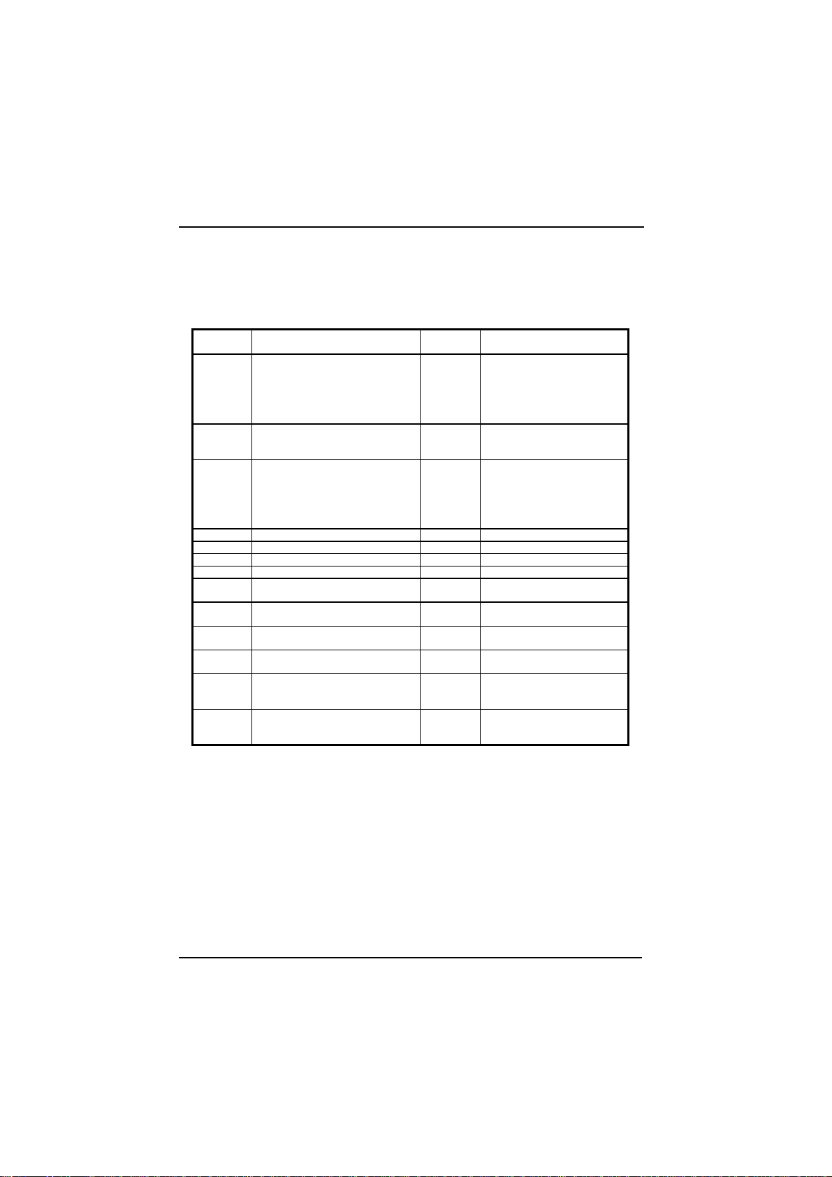
Page 14 User Gui de
3.2.1 Start-up Configurations for Option Jumpers
The link settings shown below are the default settings and not the only ones
possible. Please refer to Appendix C for the full list of options.
Jumper Area of Influence Default
J1 Selects the frequency of the on
board clock which drives the
microprocessor. Four links are
used numbered 1, 2, 3 and 4.
A = Link Absent
P = Link Present
J2 Selects 486 SX or DX operation
Two links are fitted for DX option
and one link for SX option
J3 Selects the LCD Display type to be
interfaced.
Three links are used for this
numbered 1,2, and 3.
Please see Appendix M for more
information.
J4 On Board Video Control 2 - 3 On board video Enabled
J5 Power Save Switch Open Do not use
J6 IDE Ground Link Link P12 Pin 34 shorted to ground
J7 LPT Printer IRQ Selection 1 - 2 IRQ 7 Selected LPT 1
J8 Selects either Internal or External
Battery supply
J9 CMOS Battery Clear
Connects to power CMOS
J10 Selects the control mode of serial
port 1 P12 if used in RS485 mode
J11 Selects the control mode of serial
port 2 P12 if used in RS485 mode
J12 Selects Processor Type
3 pins adjacent to J2
(Pin1 at top)
J13 Selects Processor Voltage
4 pairs of pins adajcent to J2
(Pin 1 at top)
Link
1 2 3 4
P A P A
A A P A
1 2 3 4
1-2 3-4
2 - 3
1 2 3
A A P
A P P
P A P
P P P
2 - 3 Selects Internal Battery
1 - 2 Battery Connected
None Full Duplex Selected
None Full Duplex Selected
1 - 2
2 - 3
1 2 3 4
A A A A
P P P P
Processor Freqy.
25 MHz
33 MHz
The defaults are processor
dependent. See Appendix C
Processor Dependent
486 DX
486 SX
Display Type Dependent
TFT Colour 9/12/18 bits
Monochrome Dual Scan
STN Colour Dual Scan
STN Colour Single Scan
Processor Dependent
486 DX or SX
P24T
Processor Dependent
3V3 CPU
5V CPU
Action
127-171.doc Blue Chip Technology Ltd.
Page 25

User Guide Page 15
p
y
3.3 Connecting to the I/O headers
3.3.1 Connecting the Power Lead
Locate th e con nect or P13 (a 5 ¼" di sk dr i ve type conn ector) at on e corn er of t he
PCB. Either connect the cable labelled Power to this connector or wire the
connector as shown below. The use of an in-line fuse is recommended.
Standard PC
P.S.U
Fuse
+ 5V
0V Gnd
+ 12V
-5V
P19
1 2 3
4
3
2
1
-12V
P13
+ 5V
0V GND
+12 Volt
(Not Used B
3 Am
RED
BLACK
YELLOW
APEX)
PCB
PC104 Mounting Hole
WARNING
Please ensure that you follow the power wiring as shown above and not the
numbers that might be shown on any connectors you are using.
The +12 Volt input (Yellow wire) at P13, and the -5 Volt and -12 Volt
connections provided at P19 are not required for correct operation of the APEX
II unit, but may be required by either PC/104 or ISA expansion car ds. They are
provided only for compatibility with existing expansion cards.
Connector P13 P19
pin 1 +12 V pin 1 -5 V
pin 2 0 V pin 2 0 V
pin 3 0 V pin 3 -12 V
pin 4 +5 V
DO NOT SWITCH ON THE POWER SUPPLY YET.
Blue Chip Technology Ltd. 127-171.doc
Page 26
Page 16 User Gui de
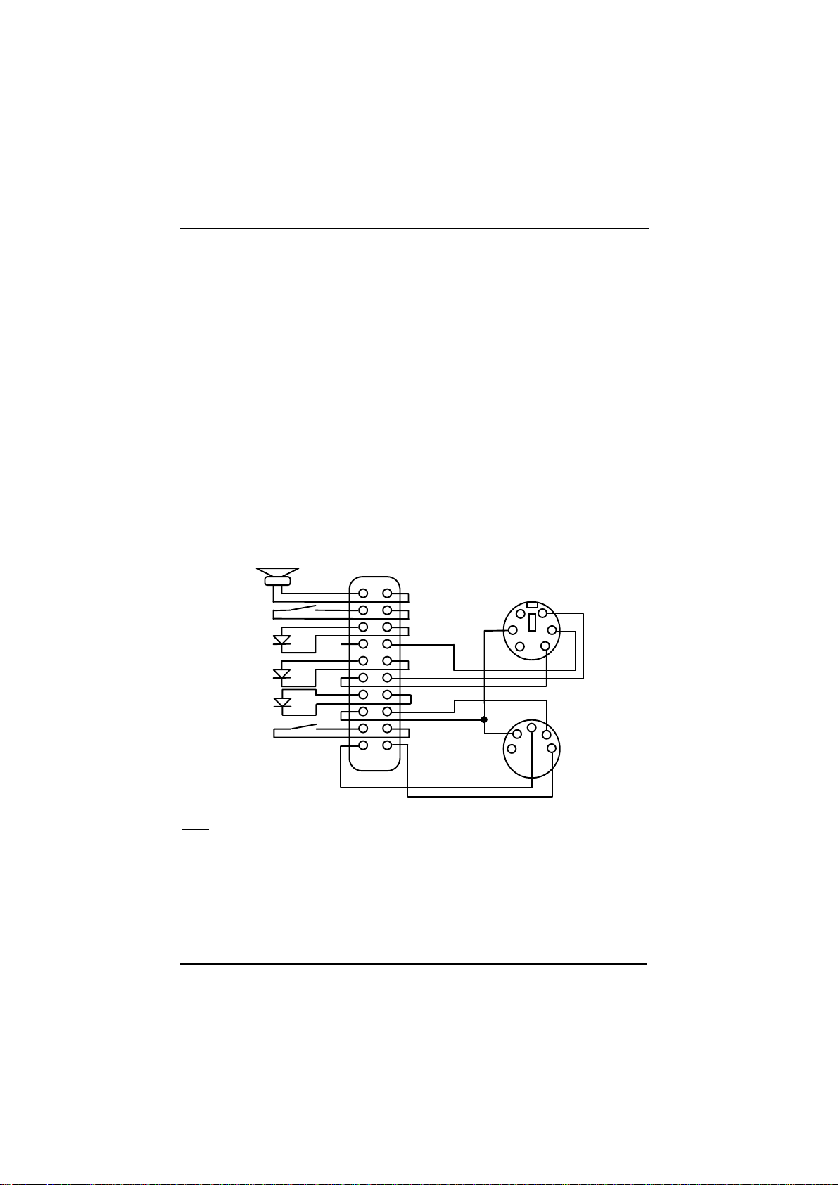
3.3.2 Connecting to the Peripherals / Utilities header
Locate connector P4 on the PCB.
This header provides connections to the following :
Keyboard.
PS/2 Mouse.
Speaker Drive.
Reset switch.
Power LED.
Turbo LED.
IDE Status LED.
Turbo Switch Input.
Either connect the optional cable labelled Perif to this connector or wire the
connector as shown below:
-Ve +ve
Reset Switch
Turbo LED
Power LED
IDE LED
Turbo Switch
Speaker
n/o
n/o
n/c
1
P4
2
19 20
PS/2 Mouse
Front View
6 Pin Mini Din
6
4
2
2
5
3
5
3
1
Rear View
Keyboard
4
5 Pin D IN
Socket
1
Note
All LED drive outputs have a 220Ω serial resistor connected to the +5 Volt
supply rail, and the +5 Volt supply to the keyboard is fused (by an SMD fuse) a t
2 Amp.
127-171.doc Blue Chip Technology Ltd.
Page 27
User Guide Page 17
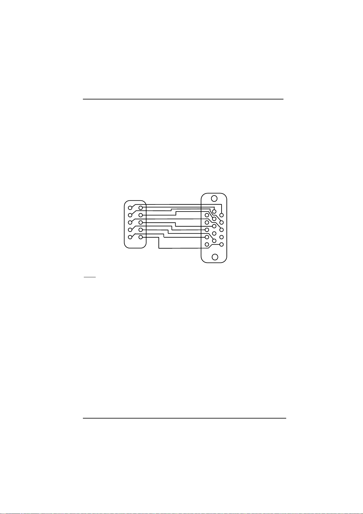
3.3.3 Connecting to the CRT Display Header
The specifications of the types of CRT displays you can use via this connector
are listed in the Technical Hardware section, but as a good starting point use
either a standard VGA or SVGA PC compatible CRT screen.
Locate connector P2 on the PCB and either connect the optional cable labelled
CRT to this connector or wire the connector as per the details below :
15 Way D Type
Condensed Version
11
Rear View
6
1
P2
1
2
9
10
15
5
10
Note
The pinout of P2 does not directly match the normal condensed 15 way D type
connector pinout used to drive CRT displays.
Please insure that you follow the above wiring diagram carefully.
We would also recommend the use of crimp style subminiature D connectors for
the CRT end of the cable.
Blue Chip Technology Ltd. 127-171.doc
Page 28
Page 18 User Gui de
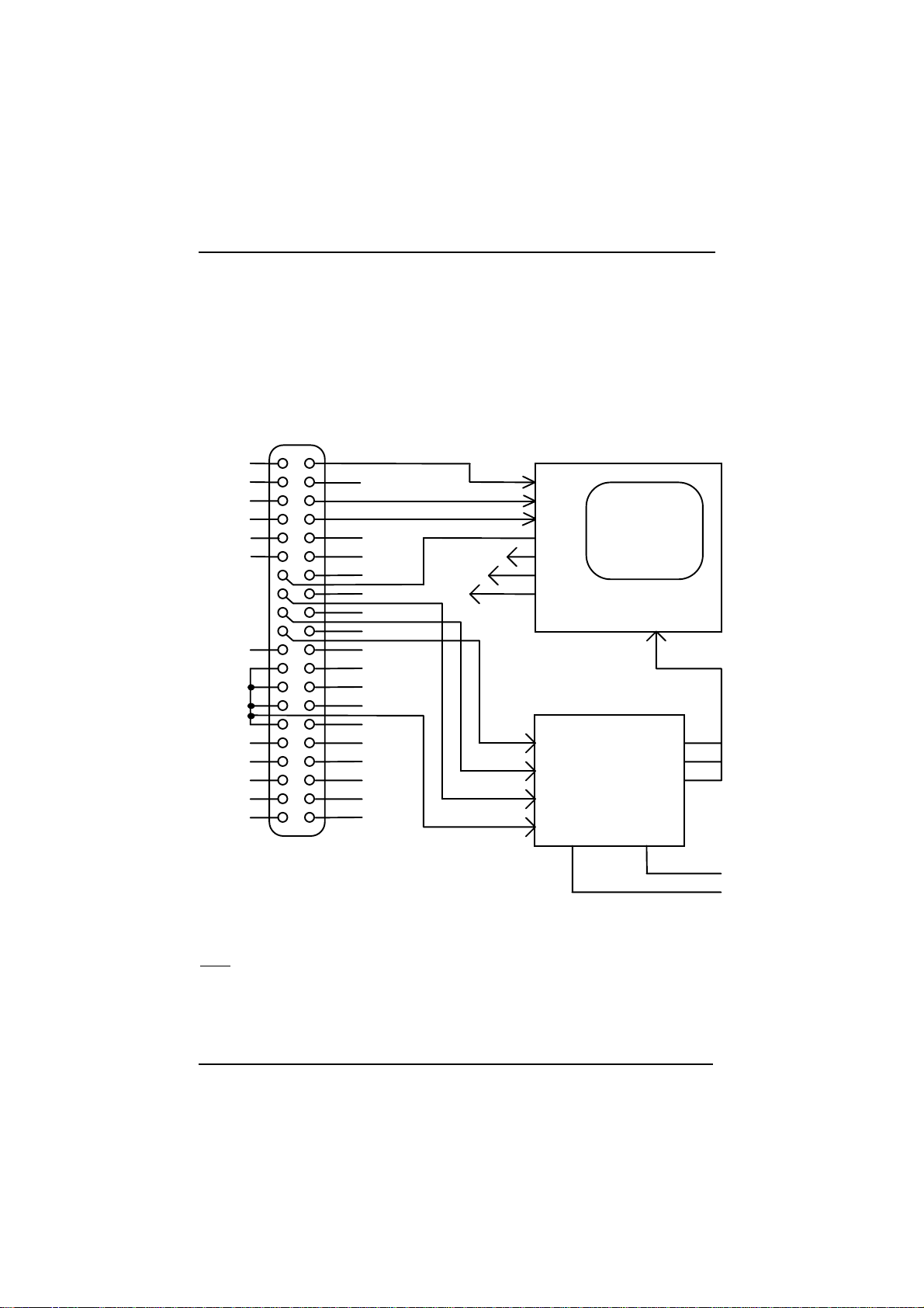
3.3.4 Connecting to the LCD Display Header
The specifications of the types of LCD displays you can use via this connector
are listed in the Technical Hardware section and Appendix M gives detailed
information on Flat Panel Interface Connection details. However, the basic
wiring concepts are shown below for guidance.
Reset
NPD
N/C
N/C
Stanby
Suspend
DE
FPback
FPVcc
FPVee
Vcc
GND
N/C
B1
B0
Vcc
+12 V
LCD Displ ay
Power In put
PWR_BIAS
PWR_LOGIC
PWR_INV
LCD_res
NPD
VEE
VLP
VBL
LCD_res
P1
1
FPVDCLK
MOD
LFS
LLCLK
R5
R4
R3
R2
G5
G4
G3
B5
B4
B3
R1
R0
G2
G1
G0
B2
DCLK
VSYNC
HSYNC
DTMG
6
6
6
R(5:0)
G(5:0)
B(5:0)
LCD Power Sequence
and Bias voltage Generation
BPO
PDO
BLO
AC Power
2
Note
A cable is not supplied for this connector due to the wide variety of displays
available.
127-171.doc Blue Chip Technology Ltd.
Page 29

User Guide Page 19
3.3.5 Connecting to the Floppy Disk Drive Header
The specifications of the floppy disk drives that can be attached are listed in the
Technical Hardware section. A 1.44 MByte 3½" disk drive is the default.
Locate the connector P8 on the PCB and connect the optional cable labelled
FDD to this conn ector and the other end to th e floppy disk dr ive. Then a dd a
power cable to the disk drive, which is part of the Development kit power
supply. Alternatively, wire the disk drive as per the details in section 3.3.5.1.
You can attach 1 or 2 disk drives to the APEX II.
The jumpers on the disk drives should be set to drive 1 not drive 0. To connect
only 1 drive, use a cable with a twist in it (between pins 10 an d 16) at the disk
drive end. For 2 drives use a daisy chain cable with the twist in the second
section leading to drive 1.
P8
Ribbon C ab le
34 Way
P8
Ribbon C ab le
34 Way
Blue Chip Technology Ltd. 127-171.doc
FDD 2
Not
Terminated Terminated
FDD 1
Terminated
Ribbon C ab le
FDD 1
34 Way
Page 30
Page 20 User Gui de
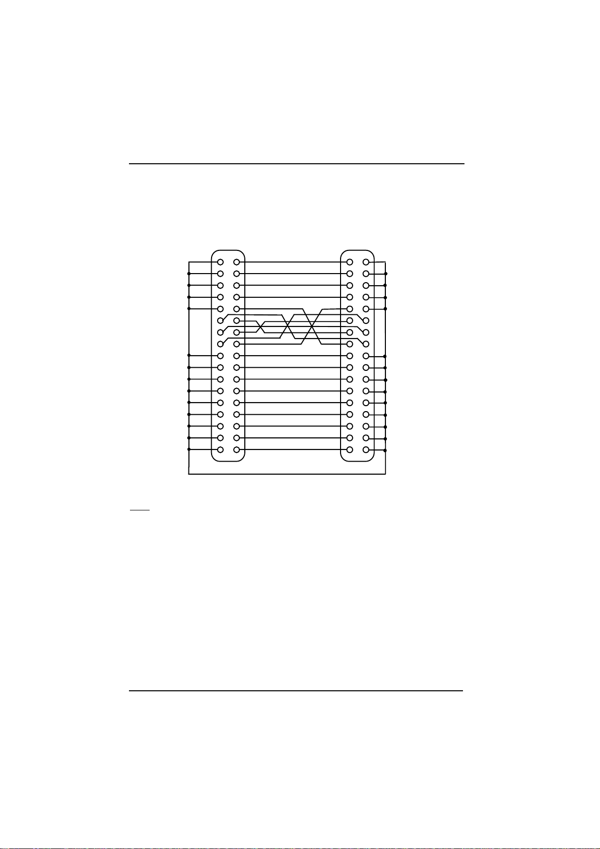
If you want t o make u p your own si n gle dr ive ca ble t hen wir e t h e conn ector s a s
follows :
P11
1
2
0V (GND)
To Floppy Disk
IDC Header
2
1
Note
Th e above wir in g is for a sin gle d isk dr ive whi ch is t erm in ated an d set to dr ive
1, not drive 0.
Also n ote tha t the ca ble is just a point to poin t IDC r ibbon ca ble with a twis t,
starting at wire 10 and going to 16.
127-171.doc Blue Chip Technology Ltd.
Page 31
User Guide Page 21
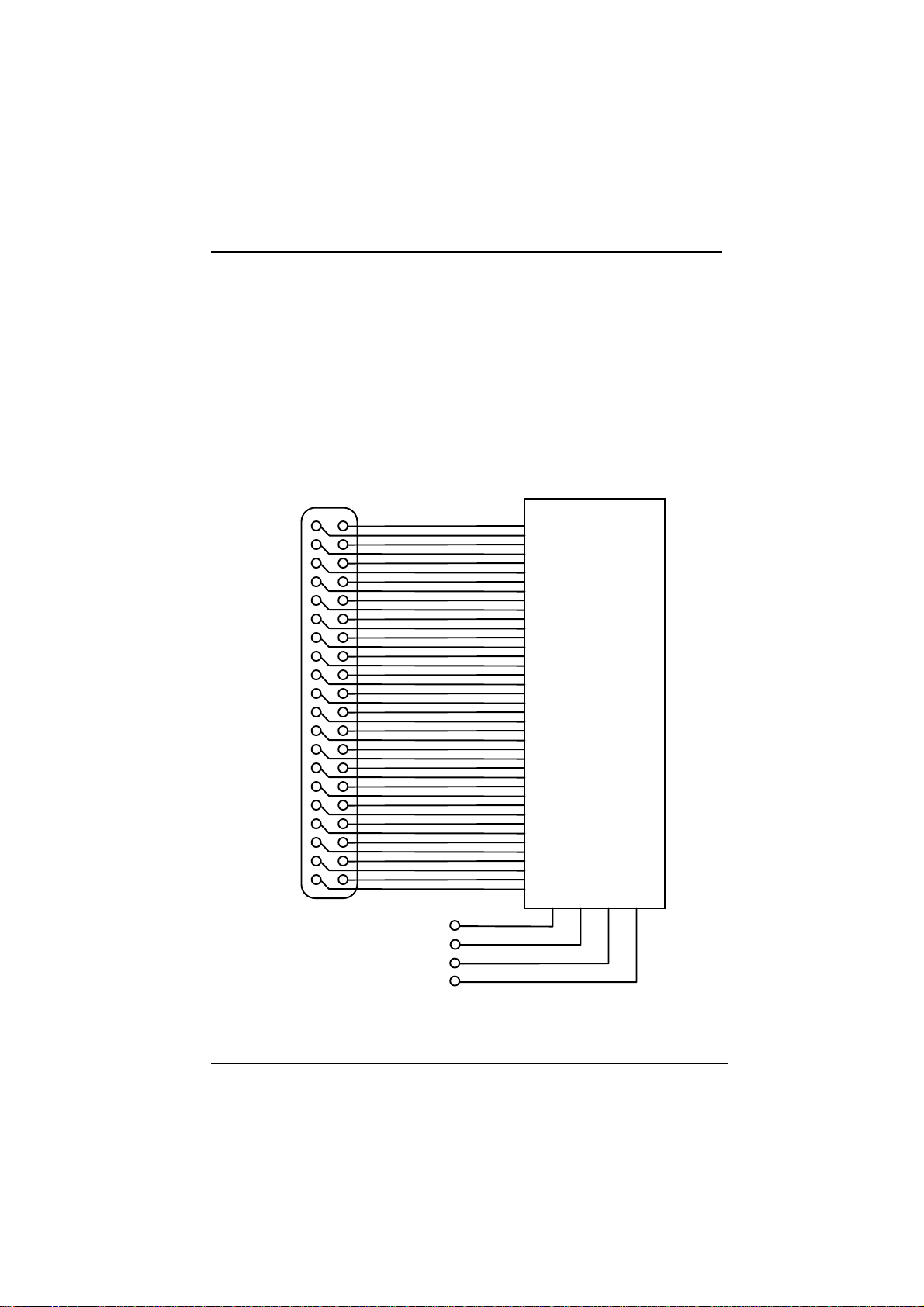
3.3.6 Connecting to the IDE Disk Drive Header
The specifications of the hard disk drives you can use via this connector are
listed in the Technical Hardware section, but as a good starting point use a
modern PC 3½" IDE drive.
Locate connector P3 on the PCB and connect the optional cable labelled IDE
HDD to this conn ector and con nect t he oth er en d to th e ha rd di sk. Th en a dd a
power cable to the disk drive, which is part of the power supply. Alternatively,
wire the disk drive as per the details below:
P3
1
:
2
IDE
Hard Disk Unit
+ 5 Volts
0V (GND)
0V (GND)
+ 12 Volts
Blue Chip Technology Ltd. 127-171.doc
Page 32
Page 22 User Gui de
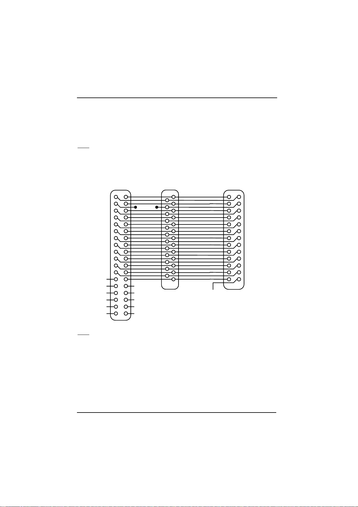
3.3.7 Connecting to the Parallel Port
Locate connector P7 on the PCB and connect the optional cable labelled PAR to
this connector. Alternatively, wire the cable as per the details below:
Note
The d irect p in out of P7 is different from that on a standard 25 way 'D' type.
This is shown below.
Centronics
36 Way Male
Connector
19
N/C
N/C
N/C
N/C
N/C
N/C
1
Cut
N/C
N/C
N/C
N/C
N/C
Rear View of
25 Way D Type
Female
14
25
P7
1
13
N/C
1
2
Note
The Centronics con nector s hown is a ID C ribbon type a nd whe n assemble d, wire
4 (pin 15 of 25 way D) MUST BE CUT for correct operation
127-171.doc Blue Chip Technology Ltd.
Page 33
User Guide Page 23
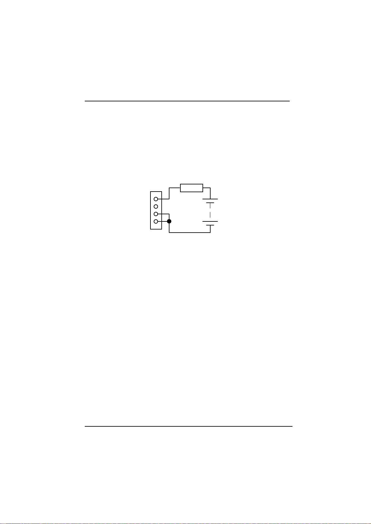
3.3.8 Connecting an External Battery
As the APEX II unit comes complete with its own on-board battery you should
not need to worry about this section. However, if your application needs an
external battery, then please follow the procedures as detailed below:
Locate connector P16 on the PCB (near the PC/104 connectors) and wire an
external battery to the diagram below:
Key way
10K Resistor
+
6 Vol t
Battery
--
P16
1
2
3
4
The battery should have an output of 6 Volts, a capacity of 1.8AH and be fitted
with a 10K series resistor for safety.
WARNING
Great care should be taken with Lithium batteries. Under NO circumstances
should :
∗ the outputs be shorted
∗ it be exposed to temperatures in excess of 100°C
∗ it be burned
∗ it be immersed in water
∗ it be unsoldered
∗ it be recharged
∗ it be disassembled
If the battery is mistreated in any way there is a possibility of fire, explosion and
harm.
Re-fit jumper J8 to short between positions 1 and 2 to select EXT battery.
Blue Chip Technology Ltd. 127-171.doc
Page 34
Page 24 User Gui de
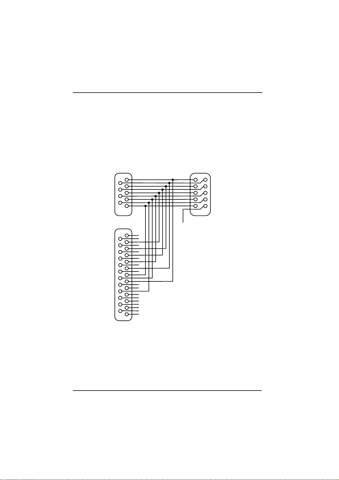
3.3.9 Connecting to the Serial Headers
Wiring 9 or 25 way 'D' types as RS232
Locate connectors P10 and P11 on the PCB and connect the cables labelled
Serial 1 and Serial 2 to these connectors. Alternatively, wire the connectors as
per the details below:
Rear View of
9 Way D Type
Male
1
6
9
5
P10 or P11
1
2
14
25
Rear View of
25 Way D Type
Female
1
N/C
13
127-171.doc Blue Chip Technology Ltd.
Page 35
User Guide Page 25
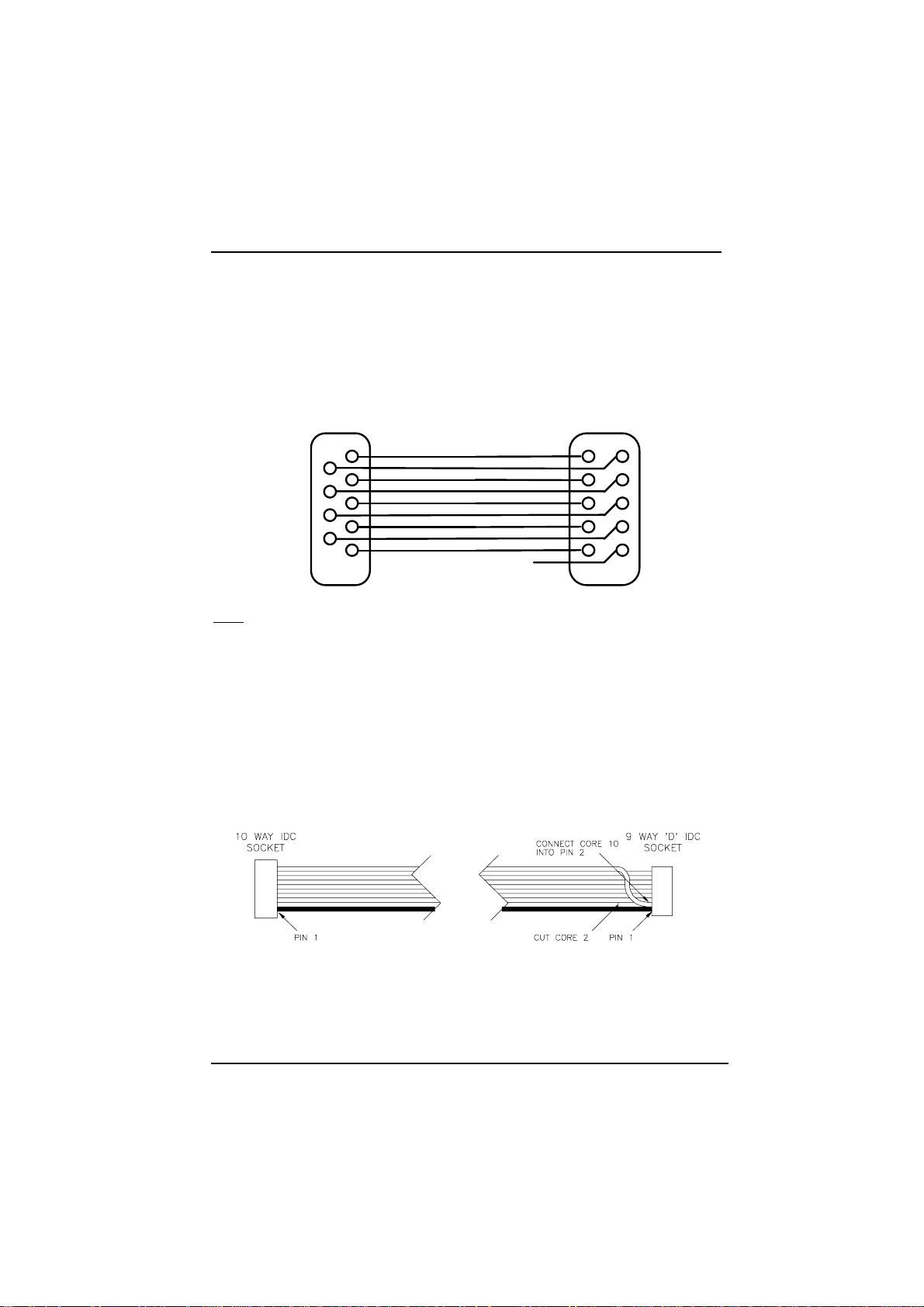
3.3.10 Wiring 9 way ‘D‘ types as RS485
Locate connector P12 on the PCB and connect the cable labelled RS485 to this
connector. Alternatively, wire the connectors as per the details below:
Rear View of
9 Way D Type
Male
P1 2
1
1
2
6
9
5
Note
Unlike the RS232 standard th ere is no recognised standard for wirin g RS485
conn ect ors. Th e above d iag ra m sh ows how our RS485 cable is wired and how
the wiring would look using standard IDC type connectors.
RS485 Port Configuration
To retain continuity, and for ease of support, APEX II units supplied with the
485 port option, should have the ribbon cable connecting the 10-way IDC
Header to the 9-way D-Type Female connector configured as :
Blue Chip Technology Ltd. 127-171.doc
Page 36

Page 26 User Gui de
This would give the following signals on the 9-way D-Type :
RS-485 Port 1 RS-485 Port 2
Pin Function Pin Function
1 Tx + 7 Tx +
2 Tx - 8 Tx 3 Rx + 9 Rx +
4 Rx - 6 Rx -
Pin 5 is GND
A 9-way Loop-Back Connector for testing purposes should be wired as follows:
Pin 1 ---------------- Pin 3
Pin 2 ---------------- Pin 4
Pin 7 ---------------- Pin 9
Pin 8 ---------------- Pin 6
127-171.doc Blue Chip Technology Ltd.
Page 37

User Guide Page 27
3.3.11 Connecting to the Digital I/O Header
Locate the connector P9 on the PCB and connect the optional cable labelled PIO
to this connector. Alternatively, wire a cable as per the details below:
Note
The Digital I/O port has many applications and as such it is impossible to
provide a definitive wiring diagram. However, the details below show the basic
wiring to a 25 way 'D' type. Appendix H at the rear of this manual gives a
complete insigh t into the workings of the 70155 PI/O and how to terminate the
outputs. All outputs can be pulled up to the Vcc rail or down to GND via th e
optional on-board 10K SIL resistor packs.
Rear View of
25 W ay D T ype
Female
1
14
P9
1
2
25
13
Blue Chip Technology Ltd. 127-171.doc
Not Used But is connected to 0V (GND)
Page 38

Page 28 User Gui de
3.3.12 Connecting to the APEX II POST Display Header
If you have the APEX II POST Dea der Displa y unit. Locate con nector P6 on t he
PCB and connect th e POST Di sp l a y unit to it. When fitted the display will show
the progress of the single board PC through the Power On Self Test which is
executed on start-up. This can assist debugging when conflicts exist.
If you do not have the APEX POST Display unit th en you will either need to
purch ase one, or build you own if you want to ma ke use of the POST Header
information.
The APEX POST Display is a self contain ed unit and is designed to be used as
part of a fault finding/diagnostic development kit.
APEX II
POST Di spla y Board
P6
12
11
12
If you require to add this function to your application as a permanent feature,
please contact Blue Chip Technology for further details on how to build your
own POST board.
127-171.doc Blue Chip Technology Ltd.
Page 39

User Guide Page 29
3.3.13 Connecting a PC/104 Module
The APEX II unit allows you to connect via the standard PC/104 stack through
PC/104 connectors, up to a maximum of three PC/104 Support Modules.
As the APEX II unit has both the XT an d AT (16 bit) connectors, any of the
currently available PC/104 units will work with this unit.
WARNING
Before connecting any external devices or cards to the APEX II unit make sure
that the power is disconnected.
Locate the connectors P15 and P17 on the PCB (connectors at the edge opposite
the S IMM sockets). Connect or P17 is t he equi valent of t he AT connect or an d
P15 is the equivalent of the XT connector.
Locate the four PC/104 mounting holes and insert 4, 16mm PCB stand-off
spacers.
To ensure that the APEX II board will operate correctly with the module, please
consult the manual that came with the unit.
Push the PC/104 card’s bus pins into the APEX's PC/104 sockets until the standoffs touch the underside of the module. Reconnect the power to the unit and
configure the system to work with your newly installed PC/104 board.
Note
For more information on the subject of driving PC/104 cards, please see the
Passive Backplane Driving section in the Hardware Technical section later in
this manual.
Blue Chip Technology Ltd. 127-171.doc
Page 40

Page 30 User Gui de
3.3.14 Connecting a Standard PC ISA Card
APEX II allows you to connect via the standard ISA slot (AT 16 bit), 1 or more
PC XT/AT expansion cards.
WARNING
Before connecting any external devices or cards to the APEX unit make sure
that the power is disconnected.
Locate the connectors P5 and P14 on the PCB (large ISA slot down one edge of
board) . Con nect or P5 is t he AT conn ector an d P14 is th e XT conn ector . Note,
however, that this pair of connectors is normally referred to as one ISA AT 16
bit connector.
To ensure that the APEX II board will operate correctly with add-on PC card,
please consult the manual that came with the PC card.
Push the PC card into the APEX's ISA sockets until the board is firmly seated.
Reconnect the power to the unit and configure the system to work with your
newly installed PC I/O card.
Note
For more information on the subject of driving PC ISA cards, please see the
Hardware Technical section later in this manual.
127-171.doc Blue Chip Technology Ltd.
Page 41

User Guide Page 31
3.4 Adding Memory
3.4.1 Adding DRAM SIMM Modules
The APEX II unit can accommodate up to two 72 pin SIMM modules using its
two SIMM sockets: SIMM1 and SIMM2.
These sockets are located on the edge of the PCB near the microprocessor. If you
ha ve or der ed th e AP EX I I wi th DRAM mem or y th en on e or both of th e s ocket s
will be occupied.
WARNING
Great care should be taken when handlin g memory devices as a build up of static
electricity can destroy them. Ensure that you touch a suitable ground to
discharge any static build up before touching the card or any new memory units.
This should be repeated if the handling is for any length of time. Always ensure
that the power is turned off before attempting to add or change memory modules.
DRAM Memory Options
Option SIMM1 SIMM2 Total DRAM
1 1MB - 1 MByte
2 1MB 1MB 2 MBytes
3 4MB - 4 MBytes
4 4MB 1MB 5 MBytes
5 4MB 4MB 8 MBytes
6 16MB - 16 MBytes
7 - 16MB 16 MBytes
Notes
• SIMM units should be a 72 pin by 36 (32 without parity) bit wide type i.e.
256K x 4 Bytes = 1MByte.
• You can use 72 pin by 32 bits wide type i.e. 4 Bytes with no parit y but you
will need to change the Set-up BIOS to action this.
• ALL SIMMs must have an access time of 70ns or faster (e.g. 60ns)
• It is possible to mix SIMM sizes. See memory options above.
Blue Chip Technology Ltd. 127-171.doc
Page 42

Page 32 User Gui de
3.4.2 Adding Flash
The APEX II unit can accommodate up to 1 additional 32 pin DIL integrated
circuit (IC) via its on-board DIL socket (IC32).
This socket is located next to the EPROM IC near the battery. If you have
ordered this unit with extra Flash (The standard build is 1MByte on-board via a
surface mount device) then this socket will be in use.
WARNING
Great care should be taken when handlin g memory devices as a build up of static
electricity can destroy them. Ensure that you touch a suitable ground to
discharge any static build up before touching the card or any new memory units.
This should be repeated if the handling is for any length of time. Also make
sure that the power is turned off before attempting to add or change memory
modules.
Flash memory can be added in one of 3 ways :
3.4.3 Standard 32 Pin Flash DIL IC's
Conventional 32 pin DIL Flash IC's from Intel or other such manufacturers can
be used. The following memory sizes were available at time of publishing :
128KBytes (P28F010A-200 or 150)
256KBytes (P28F020A-150)
512KBytes (P28F004A-150)
3.4.4 Custom 32 Pin Flash Memory Modules
By the use of Blue Chip Technology's custom made Flash Memory Modules.
These units are DIL devices and are similar to standard DIL IC's but are made
using a small PCBs with either one or two, 1MByte TSOP devices mounted on
the PCB. They are available in the following sizes :
1 MByte (971-183)
2 MBytes (971-184)
127-171.doc Blue Chip Technology Ltd.
Page 43

User Guide Page 33
3.4.5 Standard 32 Pin Flash Cards (Not PCMCIA)
A number of third party manufacturers offer credit card sized memory cards.
These cards are similar to PCMCIA cards but have a different pinout and
interface.
Blue Chip Technology has designed a remote card socket PCB which will allow
up to 1 card to be accessed by the standard on-board 32 pin Flash DIL socket.
The standard card size is 1MByte.
The part number for the Memory Card Socket is 971-185.
The drawing that follows shows its basic principle.
Memory Card Diagram
102 mm
Ribbo n Cable
32 way
Upto 450m m
32 Pin DIL Plug
Plugs int o t he FLASH IC Soc ket
Blue Chip Technology Ltd. 127-171.doc
971- 185
Memory card
PCB
Card Soc ket
Memory
Card
107 mm
Page 44

Page 34 User Gui de
The PCB has 2 sets of mounting holes. One set fits the standard 3½" floppy disk
drive mounting holes and th e other the standar d PC/104 mounting holes. Th is
allows the PCB to be used in many various ways.
Please call Blue Chip Technology for more detailed information and pricing.
3.4.6 Adding SRAM
The APEX II unit can accommodate up to one 32 pin DIL integrat ed circuit (IC)
using its on-board SRAM DIL socket (IC34).
This socket is located near to the EPROM IC and the battery. If you have
ordered this unit with SRAM memory then this socket will be in use.
WARNING
Great care should be taken when handling memory devices as a build up
of static electricity can destroy them. Ensure that you touch a suitable
ground to discharge any static build up before touching the card or any
new memory units. This should be repeated if the handling is for any
length of time. Also make sure that the power is turned off before
attempting to add or change memory modules.
SRAM memory can be added using a conventional 32 pin DIL SRAM IC. The
following memory sizes were available at the time of publishing:
128 KByte HM628128
512 KByte HM628512
These may be up to 150 nS access time, but must be low power parts.
Note: Large SRAM Modules will require an external battery to preserve the
contents. If the on-board battery remains connected (Jumper J8) it will be
discharged at a greater rate.
127-171.doc Blue Chip Technology Ltd.
Page 45
User Guide Page 35
ppy
y
g
pply
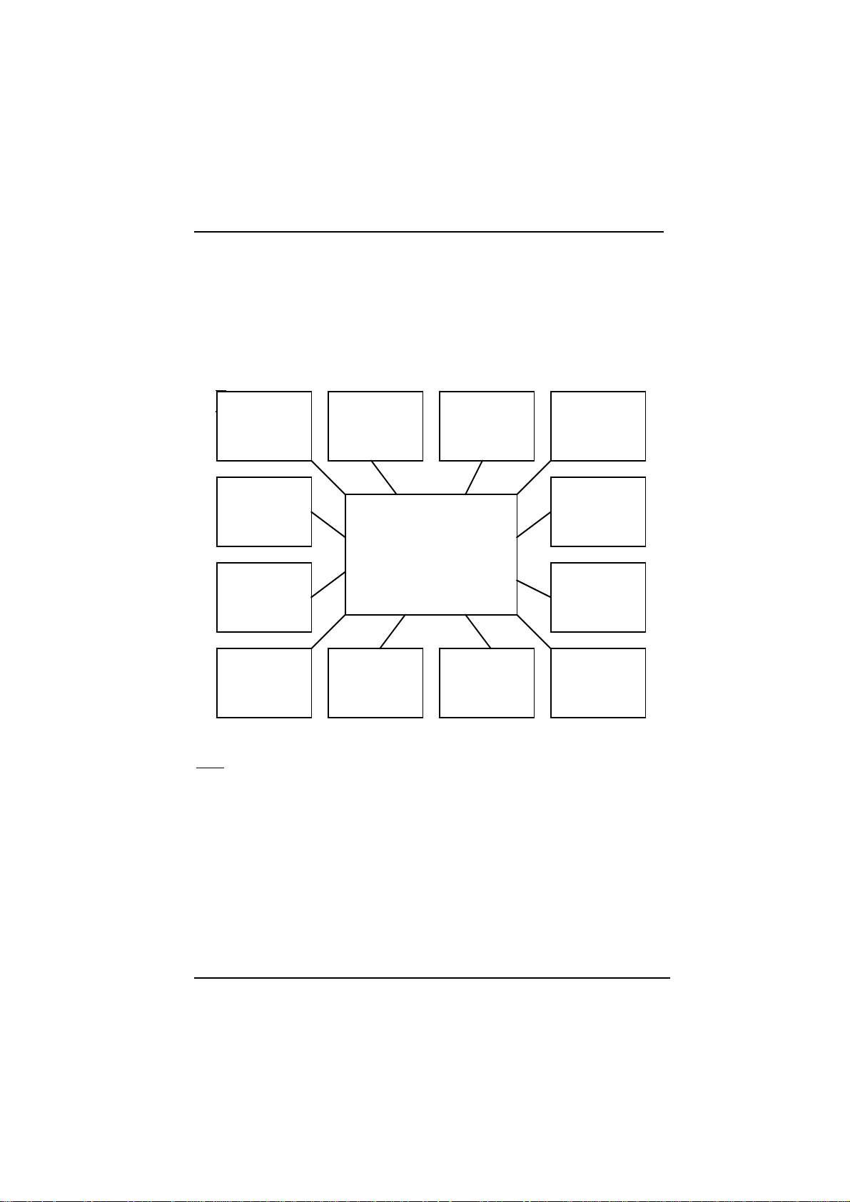
3.5 Final wiring checks
The completed APEX II assembly
The block diagram below shows functionally a completely assembled unit. It
would be advantageous at this point to re-check any of the connections you have
made to the unit whilst using the User Guide.
Displays Flo
LCD/CRT
Disk Dri ve
On-board
SSM
Flash/SRAM
APEX II SBC
IDE
Disk Dri ve
Ke
board
and Mouse
Serial Port
1
486SX25 - P24T/83
Power
Su
PC104 and or
PC AT card
POST
Header
Di
ital I/O
Port
Serial Port
2
Parallel Port
Note
The diagram is intended to show the total flexibility of the APEX II unit NOT
the actual connector positions. Please see Appendix B for a PCB plot which will
indicate the actual positions.
Blue Chip Technology Ltd. 127-171.doc
Page 46

Page 36 User Gui de
3.6 Connecting the power and switching on
Before you finally switch the unit on please ensure that the unit IS NOT on a
conductive surface.
You must also make sure that you have some form of Operating System (e.g. MS
DOS) loaded onto one of the connected disk drives, or that you are using the
remote disk drive function to access the floppy disk drive of another PC. Please
consult your chosen operating systems manual for set-up procedures.
You can now switch the unit on and if all is well, the unit should power up like a
normal desk top PC.
IMPORTANT NOTES
Due to the way the BIOS is stored in the EPROM (it is a compressed file and has
to uncompress first), the APEX unit will take about 10 seconds to display
anything onto a connected screen. This action is correct and not a fault of the
unit.
If you are runn ing DOS th en after th e AMI BIOS has checked the system, t he
unit will load and run DOS or any other application you have instructed the
AUTOEXEC.BAT file to run (e.g. Windows).
If for any reason this does not happen please refer to the Trouble Shooting
section which follows.
127-171.doc Blue Chip Technology Ltd.
Page 47

Troubleshooting Guide Page 37
4. TROUBLESHOOTING GUIDE
4.1 Introduction
In the Troubleshooting Guide we have tried to list some of the most common
problems we have encountered or can imagine. This main section is sub-divided
into 13 sub-sections which should enable you to solve the particular problem you
have.
It must be noted at this point that we have assumed that you have read and
carefully followed the connection details as described in the USER GUIDE
section of this manual and that the jumper links are as detailed in part 3.2.1 of
that section.
If this is the case please move onto section 4.1.1.
However, if the above is n ot the case and you have altered any of the jumper
links or have altered the AMI BIOS start-up settings, then please follow the
steps detailed below before moving onto section 4.1.1.
4.1.1 Resetting the APEX II Unit to a Known State
Firstly, make sure that ALL of the jumper links are as detailed in section 3.2.1.
Then reset the CMOS RAM tha t defines the config uration of the APEX II by
using jumper J9. Change the link to position 2-3.
Leave this connected for 5 minutes and then return J9 back to its original
position (across pins 1 and 2).
This action will cause the CMOS RAM to clear an d any altered BIOS setting
will be lost. The BIOS will now load its default settings when you reconnect the
power.
4.2 Power Supply Problems
Always check the power supplied to APEX II before exploring other potential
problems.
Blue Chip Technology Ltd. 127-171.doc
Page 48

Page 38 Troubleshooting Guide
Is there +5 Volts actually getting to the +5 Volt pin on the APEX power
connector when referenced to the GND input pin, and is the APEX II power
connector the right way round ?
Is the power supply capable of supplying the curr ent r equired to operate not only
the APEX II unit but any other connected items ?
Are all of the power connections of the other items connected to the APEX II
unit wired correctly ?
Is the voltage supplied between 4.9 Volts and 5.1 Volts ?
If th e a n swer s t o th e a bove que sti on s a re YES , t h en it i s u n li kel y th a t th er e i s a
power supply problem.
4.3 BIOS Start up Problems
The BIOS is fundamental to the correct operation of the unit and as such you
should read the Software Technical section now if the unit is not getting past the
basic BIOS start up routines.
If after reading the Software Technical section you still can not get the unit to
start up correctly, please read Appendix L at the rear of this manual on
contacting the Technical Support department.
4.3.1 BIOS is losing configuration set-up
Most of the changes you make to the BIOS set-ups are held in battery backed
CMOS RAM by the on-board battery with some being held in the E
2
PROM
device. If after altering the BIOS settings you get the old/default BIOS values
back at th e next p ower on of the uni t, then t he CMOS RAM is losing its power
supply.
Check to see if link J8 is set incorrectly to external battery supply, or that link J9
is not set to clear the CMOS RAM.
If both of these links are set correctly for your mode of operation then the only
item left is the battery itself.
127-171.doc Blue Chip Technology Ltd.
Page 49

Troubleshooting Guide Page 39
If you check to see what voltage level is across the on-board battery, please do so
with the main power input disconnected.
The reading should be about 3.6 Volts. If it is below 3.0 Volts then the battery
will need replacing. Please read the battery section of the Technical Hardware
section before attempting to tamper with the battery.
4.3.2 APEX II Unit Beeps at you at power on
If the APEX II unit beeps at you when you are in a power on reset state, then
consult the BIOS Beep codes Appendix G section 13.1 to determine the possible
cause.
4.4 CRT Screen Problems
Display problems are normally quite straightforward to correct.
Are ALL of the wires fr om the AP EX CRT disp lay connect or conn ected to th e
correct pins of the 15 way condensed 'D' type and are they all electrically sound ?
Is the Video enabled on the APEX unit ? Check J4 is set correctly i.e. across
pins 2 and 3.
Is the display a standard VGA or SVGA PC screen ?
Has the scr een previ ously worked on a PC before bein g conn ected to t he APEX
II unit ?
If the display shows no information at all, check that th e CPU links J1 are fitted
correctly for the CPU fitted.
If the display shows the correct information but the colours are wrong and you
have checked the wiring of the display cable it indicates that one or more of the
outputs from the display driver is not working. If there is still no display, please
call Blue Chip Technology for assistance.
Blue Chip Technology Ltd. 127-171.doc
Page 50

Page 40 Troubleshooting Guide
4.5 Flat Panel Display Problems
Due to the nature of these types of displays it is very difficult to give a good level
of troubleshooting answers. However, as a basic guide the most common
problems are power supply and display data pin configuration. If you are happy
that you have wired the display to the LCD connector output P1 correctly and
that the power to the display is correct, please call our Technical Support
department for assistance.
Please note that in most cases the display information will be feed via a power
sequencing board which provides power sequencing an d control of the contrast
and brightness. If you are using this type of board, make sure that power is
applied to the separate power input connectors and that the output form this card
is good.
4.6 Keyboard and Mouse Problems
As the APEX II unit does not emp loy the st andard mini DIN sockets, possible
wiring problems can occur when connecting the keyboard and mouse to the
Utilities connector.
Please make sure that the wiring is correct and that there is +5 Volts getting to
both units. If the +5 Volt line which feeds the keyboard and mouse is not
present when the main power is connected, then it is likely that the on-board 1
Amp fuse has blown.
This fuse is a Surface Mount Device and is located next to the Utilities connector
below a mounting hole. Please call Blue Chip Technology for assistance if you
need this fuse changing.
4.7 Memory Problems
The APEX II unit can employ three types of memory fitted by the user. These
are DRAM, FLASH and SRAM. Each type of memory has its own set of
potential problems which are now dealt with below.
127-171.doc Blue Chip Technology Ltd.
Page 51

Troubleshooting Guide Page 41
4.7.1 DRAM Memory Problems
The APEX II unit uses up to two 72 pin DRAM SIMM modules and can
accommodate up to 32MBytes in these sockets. The DRAM memory must have
an access time of 70nS or better (e.g. 60nS) but can be either with, or without,
PARITY. If the DRAM modules you are using are of a non-pari ty type, please
make sure that the BIOS is configured for this.
The SIMM sockets we have chosen are of a good mechanical design and should
cope with most industrial applications. Always ensure that the DRAM memory
you install is firmly seated into the sockets and that they are the correct way
round.
4.7.2 Flash Memory Problems
Flash on the APEX II unit i s supported in two ways: an on-board 1MByte TSOP
device and a 32 pin DIL socket. When using the 32 pin DIL socket please make
sure that the device is inserted the correct way round. If you are having
problems reading or writing to this form of memory please consult both the
Software Technical and the Flash Programming Appendix I for more in-depth
information.
4.7.3 SRAM Memory Problems
SRAM on th e APEX II unit is supported by a 32 pin DIL socket. Wh en using
the 3 2 pin DIL s ocket pl ease make su re that the device is inser ted th e correct
way round. If you are having problems reading or writing to this form of
memory please consult both the Software Technical section and the Memory
Map Appendix N for more in-depth information.
4.8 Floppy Disk Drive Problems
The most common floppy disk problems are that of connections to the host PC’s
connectors and their settings. Please make sure that the cable used to provide
data is connected to both the APEX II unit and the floppy disk unit the correct
way round and that the disk drive is set to the correct drive setting (1 or 0) for
the cable you are using. Please refer to the User Guide for more information.
Blue Chip Technology Ltd. 127-171.doc
Page 52

Page 42 Troubleshooting Guide
If the floppy disk still fails to operate after checking the above, pl ease try the
disk unit on another PC to ascertain if the disk is at fault or whether the
APEX II controller device may have a problem.
Please call our Technical Support department for assistance if the latter proves to
be the problem.
4.9 IDE Hard Disk Problems
Most IDE hard disk drives give little trouble if configured correctly (see the
Software Technical section about Auto Select Hard Disk Drives. The pointers
lis ted i n s ecti on 4. 8 a bove will be true for IDE drives with the exception of the
drive selection values 1 and 0.
If the hard drive still fails to operate even after checking the above, pl ea se t ry th e
hard disk unit on another PC to make sure if the disk is at fault or whether the
APEX II controller device may have a problem.
Please call our Technical Support department for assistance if the latter proves to
be the problem.
4.9.1 Auto-detect IDE Hard Disks
When in the BIOS SETUP mode and trying to auto-detect hard disk drives
connected to the APEX IDE port, the BIOS will not see the disk drive on the
very first attempt if the CMOS RAM has been cleared.
You must save any other changes you have made and then re-enter the BIOS
SETUP and auto-detect the IDE disk drives again.
You will find that on the second attempt the disk(s) will be located correctly.
This is a BIOS error and not a hardware fault and we are currently awaiting a
fix from AMI.
4.10 Serial Problems
The serial ports on the APEX II unit can be set for either RS232 or RS485.
Please make sure that the BIOS settings are correct for your application needs.
127-171.doc Blue Chip Technology Ltd.
Page 53

Troubleshooting Guide Page 43
Part of the set of cables provided with either the Development kit or the APEX II
test wiring kit is a serial loop back tester. Connect this cable between the two
serial ports and run the Serial Test Program (Serial_T.exe) on the APEX II
Software Utilities Disk.
4.10.1 RS485 Serial Problems
When using the serial ports in RS485 mode, check that you have the full/half
duplex jumper links set correctly. Please refer to section 4.0 of the Hardware
Technical section for more information.
4.11 Parallel Problems
The parallel port of the APEX II unit can be set to either uni or bi-directional
mode. Please check the BIOS setting for correct operation. Check jumper link
J7 to insure correct IRQ settings. Check the cable wiring (see User Guide).
4.12 Digital I/O Problems
Ensure that the BIOS is set correctly for your applications needs. Using a
parallel loop back test cable run a simple loopback test program. If you require
help with this ask for a copy of APEX II test program DIGIO_T.EXE.
Please refer to Appendix H for an in-depth look at the operation of the digital
I/O port.
4.13 PC/104 and PC XT/AT Card Problems
Almost all of the problems encountered when trying to access another card
connected either via the PC/104 bus or the ISA slot are related to configuration
of the host system, in this case the APEX II unit or the setup of the card being
attached.
The card(s) that are to be added will be supplied with a set-up manual which
explains how to configure the host PC. Please read this information carefully
and alter the BIOS settings accordingly.
If you are using more than one ISA card (normally in a PC riser card), make
sure that the connections are sound and that the bus termination, if used is
Blue Chip Technology Ltd. 127-171.doc
Page 54

Page 44 Troubleshooting Guide
correct. Please refer to the Hardware Technical section for a more in-depth look
at using these connectors.
127-171.doc Blue Chip Technology Ltd.
Page 55

Troubleshooting Guide Page 45
4.14 Using the APEX II unit with a Host PC
The APEX II unit can be operated in conjunction with a h ost PC. Please refer to
Appendix I section 15.2 for a more in-depth information.
Blue Chip Technology Ltd. 127-171.doc
Page 56

Page 46 Hardware Technical Section
5. HARDWARE TECHNICAL SECTION
5.1 Introduction
This section of the manual cover all aspects of the APEX II hardware
specifications and should be read fully before attempting to alter or interface
with any of the on-board electronics.
5.2 APEX II ISA and PC/104 Bus Signal Descriptions
The following sections describe the functions of all of the standard ISA and
PC/104 bus signals. All signal lines are TTL compatible.
5.2.1 AEN (O)
'Address Enable' is used to negate the microprocessor and other devices from the
I/O channel to allow DMA transfers t o take place. Wh en th is lin e is active, th e
DMA controller has control of the address bus, the data-bus Read command
lines (memory and I/O), and the Write command lines (memory and I/O).
5.2.2 BALE (O) (Buffered)
'Address latch enable' is provided by the bus controller and is used on the system
board to latch valid addresses and memory decodes from the microprocessor. It
is available to the I/O channel as an indicator of a valid microprocessor or DMA
address (wh en used with 'AEN' ). Microprocessor addr esses SA0 thr ough SAl9
are latched with the falling edge of 'BALE. ' 'BALE' is forced high during DMA
cycles.
5.2.3 CLK (O)
This is the system clock. The clock has a 50% duty cycle. This signal should
only be used for synchronisation. It is not intended for uses requiring a fixed
frequency.
5.2.4 -DACK0 to -DACK3 and -DACK5 to -DACK7 (O)
-DMA Acknowledge 0 to 3 and 5 to 7 incl usive are used to ackn owledge DMA
requests (DRQ0 to DRQ7). They are active low.
127-171.doc Blue Chip Technology Ltd.
Page 57

Hardware Technical Section Page 47
5.2.5 DRQ0 to DRQ3 and DRQ5 to DRQ7 (I)
DMA Requests 0 to 3 and 5 to 7 inclusive are asynch ronous chan nel requests
used by peripheral devices and the I/O channel microprocessors to gain DMA
service (or control of the system). They are prioritised, with DRQ0 having the
highest priority and DRQ7 having the lowest. A request is generated by bringing
a DRQ line to an active level. A DRQ line must be held high until the
correspondi ng ' DMA Request Acknowledge' (DAC K) lin e goes active. DRQ0 to
DRQ3 will perform 8 -bit DMA transfers; 'DRQ5' to DRQ7 will perform l6 bit
transfers.
5.2.6 -I/O CHCK (I)
'-I/O channel check' provides the system board with parity (error) information
about memory or devices on the I/O channel. When this signal is active, it
indicates an in correctable system error.
5.2.7 I/O CHRDY (I)
'I/O channel ready' is pulled low (not ready) by a memory or I/O device to
lengthen I/O or memory cycles. Any slow device using this line should drive it
low immediately upon detecting its valid address and a Read or Write command.
Mach ine cycles are ex tend ed by an in tegr al n umber of cl ock cycles. Th is sig nal
should be held low for no more than 2.5 microseconds.
5.2.8 -I/O CS16 (I)
'-I/O 16 bit Chip Select' signals the system board that the present data transfer is
a 16 bit, 1 wait state, I/O cycle. It is derived from an address decode. '- I/O CS
16' is active low and should be driven with an open collector or tri-state driver
capable of sinking 20mA.
5.2.9 -IOR (I/O)
'-I/O Read' instructs an I/O device to drive its data onto the data bus. It may be
driven by the system mi croprocessor or DMA con troll er, or by a microprocessor
or DMA controller resident on the I/O channel. This signal is active low.
Blue Chip Technology Ltd. 127-171.doc
Page 58

Page 48 Hardware Technical Section
5.2.10 -IOW (I/O)
'I/O Write' instructs an I/O device to read the data on the data bus. It may be
driven by any micr oprocessor or DMA cont roller in the system. This sig nal is
active low.
5.2.11 IRQ3 to IRQ7, IRQ9 to IRQ12 and IRQ14 to 15 (I)
Interrupt Requests 3 through 7, 9 through 12, and 14 through 15 are used to
signal the microprocessor that an I/0 device needs attention. The interrupt
requests are prioritised, with IRQ9 through IRQ12 and IRQ14 through IRQ15
having the highest priority (IRQ9 is the highest) and IRQ3 through IRQ7 having
the lowest priority (IRQ7 is the lowest). An interrupt request is generated when
an IRQ line is raised from low to high. The line must be held high until the
microprocessor acknowledges the interrupt request (Interrupt Service routine).
5.2.12 LA17 to LA23 (I/O)
These signals (unlatched) are used to address memory and I/O devices within th e
system. They give the system up to 16MB of address capability. These signals
are valid when 'BALE' is high. LA17 through LA23 are not latched during
microprocessor cycles and therefore do not stay valid for the whole cycle. Their
purpose is to generate memory decodes for 1 wait-state memory cycles. These
decodes should be latched by I/O adapters on the falling edge of 'BALE. ' These
signals also may be driven by other microprocessors or DMA controllers that
reside on the I/O channel.
5.2.13 Master (I)
This signal is used with a DRQ line to gain control of the system. A processor or
DMA controller on the I/O channel may issue a DRQ to a DMA channel in
cascade mode and receive a '- DACK'. Upon receiving the '- DACK', an I/O
microprocessor may pull '- Master' low, which will allow it to control the system
address, data, and control lines (a condition known as tri-state). After '- Master'
is low, the I/O microprocessor must wait one system clock period before driving
the address and data lines, and two clock periods before issuing a Read or Write
command. If this signal is held low for more than 15 microseconds, system
memory may be lost because of a lack of refresh.
127-171.doc Blue Chip Technology Ltd.
Page 59

Hardware Technical Section Page 49
5.2.14 -MEMCS16 (I)
'-MEM 16 Chip Select' signals the system board if the present data transfer is a 1
wait-state, 16 bit, memory cycle. It must be derived from the decode of LA17
through LA23. '-MEM CS 16' should be driven with an open collector or tristate driver capable of sinking 20mA.
5.2.15 OSC (O)
'Oscillator' (OSC) is a high speed clock with a 70 n anosecond period (14.31818
MHz). This signal is n ot synchronous with th e system clock. It has a 50% duty
cycle.
5.2.16 -0WS (I)
The 'Zero Wait State' (0WS) signal tells the microprocessor that it can complete
the present bus cycle without inserting any additional wait cycles. In order to run
a memory cycle to a 16 bit device without wait cycles, '0WS' is derived from an
address decode gated with a Read or Write command.
In order to run a memory cycle to an 8 bit device with a minimum of two wait
states, '0WS' should be driven active on system clock after the Read or Write
command is active gated with the address decode for the device. Memory Read
and Write commands to a 8 bit device are active on the falling edge of the
system clock. '0WS' is active low and should be driven with an open collector or
tri-state driver capable of sinking 20mA.
5.2.17 -Refresh (I/O)
This signal is used to indicate a refresh cycle and can be driven by a
microprocessor on the I/O channel.
5.2.18 Reset Drive (O)
'Reset drive' is used to reset or initialise system logic at power up time or when
the power supply drops below its minimum level. This signal is active high.
Blue Chip Technology Ltd. 127-171.doc
Page 60

Page 50 Hardware Technical Section
5.2.19 SA0 to SAl9 (I/O)
Address bits 0 through 19 are used to address memory and I/O devices within
the system. These twenty address lines, in addition to LA17 through LA23,
allow access of up to 16MB of memory. SA0 through SAl9 are gated on the
system bus when 'BALE' is high and are latched on the falling edge of 'BALE. '
These signals are generated by the microprocessor or DMA Controller. They
also may be driven by other m icroprocessors or DMA cont rollers t hat r eside on
the I/O channel.
5.2.20 -SBHE (I/O)
'Bus High Enable' (system) indicates a transfer of data on the upper byte of the
data bus, SD8 through SD15. 16 bit devices use 'SBHE' to condition data bus
buffers tied to SD8 through SD15.
5.2.21 SD0 to SD15 (I/O)
These signals provide data bus bits 0 through 15 for the microprocessor,
memory, and I/O devices. D0 is the least significant bit and Dl5 is the most
significant bit. All 8 bit devices on the I/O channel should use D0 through D7
for communications to the microprocessor. The l6 bit devices will use D0
through D15. To support 8 bit devices, the data on D8 through D15 will be gated
to D0 through D7 during 8 bit transfers to these devices. 16 bit microprocessor
transfers to 8 bit devices will be converted to two 8 bit transfers.
5.2.22 -SMEMR (O), -MEMR (I/O)
These signals instruct the memory devices to drive data onto the data bus. 'SMEMR' is active only when the memory decode is within the low lMB of
memory space. '- MEMR' is active on all memory read cycles. '- MEMR' may be
driven by any micropr ocessor or DMA contr oller in th e system. '- SMEMR' is
derived from 'MEMR' and the decode of the low lMB of memory. When a
microprocessor on the I/O channel wishes to drive '- MEMR', it must have the
address lines valid on the bus for one system clock period before driving 'MEMR' active. Both signals are active low.
127-171.doc Blue Chip Technology Ltd.
Page 61

Hardware Technical Section Page 51
5.2.23 T/C (O)
'Terminal Count' provides a pulse when the terminal count (end of) for any
DMA channel is reached.
5.2.24 -SMEMW (O), -MEMW (I/O)
These signals instruct the memory devices to store the data present on the data
bus. '- SMEMW' is active only when the memory decode is within the low 1 MB
of the memory space. '- MEMW' is active on all memory write cycles. '- MEMW'
may be driven by any microprocessor or DMA controller in the system. 'SMEMW' is derived from '- MEMW' and the decode of the low lMB of memory.
When a microprocessor on the I/O channel wishes to drive '- MEMW', it must
have the address lines valid on the bus for one system clock period before
driving '- MEMW' active. Both signals are active low.
5.3 IEEE P996 Specification Information
This concludes the control bus signal description part of the Hardware Technical
Section. If you require a more in depth look at how the standard PC bus signals
are used and defined please read the IEEE P996 specification.
5.4 Video Outputs
The APEX II unit offers dual output video drive capability. By using the
CIRRUS LOGIC CL-GD6235 video controller the APEX II unit is capable of
driving both CRT and LCD displays in various modes. Connected to the video
controller is 512KBytes of video memory in the form of a single 256K x 16 bit
memory IC, (IC8). These devices offer the user a wide range of display types
giving excellent display features.
A full specification of the CIRRUS LOGIC CL-GD6235 IC is obtainable from
Blue Chip Technology Ltd. However, we have listed in the following sections
some of the more important features which we think will be of use and interest
in helping you get the most from this unit.
Blue Chip Technology Ltd. 127-171.doc
Page 62

Page 52 Hardware Technical Section
5.4.1 CRT Display Mode
The CRT outpu t P2 i s capa ble of drivin g VGA d ispl ays with r esoluti ons of up to
1024 x 768 pixels with 16 colours and 800 x 600 with 256 colours.
The 16 bit local bus interface is used to connect to the 486 microprocessor.
Using the SimulSCAN™ feature (a technique introduced by Cirrus Logic for
achieving simultaneous CRT and LCD output) you have the ability to develop
your application on a desktop PC screen and then to move over to an LCD
display with the smallest of effort. In fact you can run both displays together to
test out your display options even more quickly.
5.4.2 CRT Display Types
The Cirrus Logic 6235 display driver will drive most of the CRT display
configurations available today. If the CRT display you wish to use does not
perform in the way you think it should, please call our Technical Support
department for further information, or call your nearest Cirrus Logic dealer for
the full Data Applications Handbook. T he two di sp la y dr ive r di ske tt es s upplied
with the unit contain the most popular display drivers for both CRT and LCD
screens. More information can be found in Appendix J.
5.4.3 Flat Panel Display Modes
The flat panel output P1 is capable of driving the following display types :
Dual-Scan Monochrome LCD
Dual-Data Monochrome LCD
Passive-matrix Monochrome LCD
Colour TFT LCD (9-bit panels) *
Colour STN LCD
Dual Scan STN LCD
Monochrome EL Panels (With custom Blue Chip Video BIOS)
* (An optional custom Blue Chip Video BIOS is available for 18-bit panels)
Greyscale mapping i s provided by AutoMap™ which maps 256 colours into a
monochrome image; the colours then appear either in 16 shades of grey with
greyscale enhancement, or 64 shades of grey in 256-colour mode. Ther e a re also
four greyscale mapping options available through register control:
127-171.doc Blue Chip Technology Ltd.
Page 63

Hardware Technical Section Page 53
• NTSC weighted
• DAC Look-up table "green" output
• 4 or 6 bit video data direct
• Attribute Controller 64-shade colour data
When driving a colour STN panel it can drive 8 or 16 bit interfaces, and give
256 simultaneous colours from a palette of 256K.
When driving a colour TFT display it will support 9, 12, 15 and 18 bit panels
and give 256 simultaneous colours from a palette of 256K.
The CL-GD6235 offers true packed-pixel addressing, colour expansion for 8 bitper-pixel graphics, and a hardware cursor, thus improving Windows
performance.
5.4.4 Power Management Information
The 6235 also offers standby and suspend power-management modes which
reduce the power consumption when the system is not in active use. The
internal standby counter initiates standby mode without software intervention.
During this reduced power mode, the LCD panel is turned off while the video
memory can still be accessed and modified.
The CL-GD6235 provides efficient power mana gement of the display system by
turning off, or shutting down the LCD flat panel and CRT when not being used.
The device offers both hardware methods (using device pins) and software
methods (using programmable timers and on chip registers) to control the LCD
panel and or CRT display.
Blue Chip Technology Ltd. 127-171.doc
Page 64

Page 54 Hardware Technical Section
In Normal Mode the LCD is being used, and the following occur :
• Display is active and receives power
• Full screen refresh occurs
• CPU and access :
- Video memory
- RAMDAC
- I/O registers
• Refresh is provided to the video memory
In Standby Mode the controller stops power to the LCD panel. As a result the
following occurs :
• LCD panel power down sequence occurs automatically
when this mode is entered
• VCLK oscillator is stopped
• MCLK is divided by 6
• No clock is provided to the CRT controller
• Video DAC is in lower power mode
• Video display memory refresh is maintained
• CPU can access and modify the video memory
• When standby mode is terminated the previous state is restored
More information on power management and power sequencing is given later in
this section.
Please call our Technical Support department for further information.
127-171.doc Blue Chip Technology Ltd.
Page 65

Hardware Technical Section Page 55
5.4.5 Flat Panel Connector Pin out Details
The following table shows the pinout for the Flat Panel connector together with
a description for each pin. Note the connector is a female type and the table
shows looking down on top of the connector from the main component side of
the PCB.
Pin
N
°
2 LCDRST 1 FPVDCLK
4 NPD 3 MOD
6 FVSYNC 5 LFS
8 FHSNYC 7 LLCLK
10 STANBY 9 R5
12 SUSPEND 11 R4
14 DE 13 R3 / SUD7
16 FPBACK 15 R2 / SUD6
18 FPVCC 17 G5 / SUD5
20 FPVEE 19 G4 / SUD4
22 VCC (APEX) 21 G3 / SUD3
24 GND (APEX) 23 B5 / SUD2
26 GND (APEX) 25 B4 / SUD1
28 GND (APEX) 27 B3 / SUD0
30 GND (APEX) 29 R1 / SLD7 / UD3
32 N/C 31 R0 / SLD6 / UD2
34 B1 / SLD1 / LD1 33 G2 / SLD5 / UD1
36 B0 / SLD0 / LD0 35 G1 / SLD4 / UD0
38 VCC (APEX) 37 G0 / SLD3 / LD3
40 + 12 Volt 39 B2 / SLD2 / LD2
Description Pin
N°
Description
Note
The l abels given for th e pi nout s on con n ector P 1 ar e bia sed towar ds LCD dri ve.
If you need to contr ol a n EL pan el t hen th e pi ns t o use a re not obvi ous. Plea se
consult the Panel Interface Connection Appendix M at the rear of this manual.
LCD Signal Descriptions
5.4.6 B[5:0]
BLUE BITS [5:0]. These bits contain the BLUE colour data for TFT colour flat
panel displays.
Blue Chip Technology Ltd. 127-171.doc
Page 66

Page 56 Hardware Technical Section
5.4.7 DE
DISPLAY ENABLE. For those flat panels that require an external display
enable, this pin is used to provide a data enable. For the CL-GD6235 it is the
second Shift Clock output for STN single-scan dual-clock colour panels.
5.4.8 FPVDCLK
FLAT PANEL VIDEO CLOCK. Th is si gn al is used to d r ive th e flat panel shift
clock which is designated as CP0 by some panel manufactures.
5.4.9 G[5:0]
GREEN BITS [5:0]. These bits contain the Green colour data for TFT colour
flat panel displays.
5.4.10 LD[3:0]
LOWER DATA [3:0]. The lower Data bits [3:0] are typically used with
monochrome dual-scan flat panels to provide 4 bit parallel data for the lower
portion of the panel.
5.4.11 LFS
LCD FRAME START. This output provides a pulse to start a new frame on flat
panels.
5.4.12 LLCLK
LCD LINE CLOCK. This output is used to drive the LCD panel line clock.
This signal is also designated as LP or CP by some panel manufacturers.
5.4.13 MOD
MODULATION. Thi s output pr ovides AC in versi on. I t sh ould be conn ected to
the MOD, FR or DF inputs of the panel, and is appropriate. Some panel
manufacturers provide this function in the panel circuitry.
127-171.doc Blue Chip Technology Ltd.
Page 67

Hardware Technical Section Page 57
5.4.14 R[5:0]
RED BITS [5:0]. These bits contain the Red colour data for TFT colour flat
panel displays.
5.4.15 SLD[7:0]
STN LOWER DATA [7:0]. The lower data bits [7:0]are for use with colour
STN LCD panels.
5.4.16 SUD[7:0]
STN UPPER DATA [7:0]. The upper data bits [7:0] are for use with colour
STN LCD panels.
5.4.17 UD[3:0]
UPPER DATA. The Upper Data bits [3:0] are typically used with monochrome
dual-scan flat panels to provide 4-bit parallel data for the upper portion of the
panel.
5.4.18 LCDRST
LCD Reset. This active low signal is an optional LCD display reset input. Any
logic high to low transition on this input will clear both the LCD and CRT
enable bits in the power management register (CR20[6:5]). This will initiate the
LCD-panel power down sequence, and will stop video memory refresh.
The logic high to low transition on this pin does not restore the CRT or LCD
enable bits. These bits must be restored by writing to the appropriate registers.
This pin has an internal pull-up resistor. Avoid connecting to the pin if the
function is not used.
5.4.19 STANDBY (Input or Output function pin)
When the panel is on and this input is driven high, the power down sequence
will start to put the system into Standby Mode. Standby Mode terminates when
this pin goes low, as long as CR20[4] =' 0 ' and the standby timer has been reset.
Blue Chip Technology Ltd. 127-171.doc
Page 68

Page 58 Hardware Technical Section
Please ask for more detailed information if your application needs to make use of
this function.
5.4.20 SUSPEND
This input pin can be used in one of two ways :
1. To initiate the Hardware Suspend mode. If the Suspend pin is used to
control Suspend Mode, CPU access will not be allowed.
2. To turn off the LCD display for a 'closed cover' type condition. In a closed
cover type condition, CPU access is allowed, and the CRT outputs remain
active.
Please ask for more detailed information if your application needs to make use of
this function.
5.4.21 FPBACK (Output pin)
Flat Panel Backlight. This output pin is part of the panel power sequencing, and
it should be used to drive a suitable power controller switch (e.g. Mosfet
transistor) which in turn will be connected to the panels backlight power input
pin. If you are using the LCD-PSU controller boards the power sequencing
function of this output is taken care of. Please see Appendix M for more details.
5.4.22 FPVCC (Output pin)
Flat Panel VCC. This output pin is part of the panel power sequencing, and it
should be used to drive a suitable power controller switch (e.g. Mosfet transistor)
which in turn will be connected to the panels VCC power input pin. If you are
using the LCD-PSU controller boards the power sequencing function of this
output is taken care of. Please see Appendix M for more details.
5.4.23 FPVEE (Output pin)
Flat Panel VEE. This output pin is part of the panel power sequencing, and it
should be used to drive a suitable power controller switch (e.g. Mosfet transistor)
which in turn will be connected to the panels VEE power input pin. If you are
using the LCD-PSU controller boards the power sequencing function of this
output is taken care of. Please see Appendix M for more details.
127-171.doc Blue Chip Technology Ltd.
Page 69

Hardware Technical Section Page 59
5.4.24 NPD (Input pin)
NO POWER-DOWN. This pin, when 'high', stops the power down counters
from decrementing. This pin is used to inhibit automatic power down when, for
example, the system is supplied from an AC power source.
5.4.25 FVSYNC
VERTICAL SYNC. This is a copy of the vertical sync lin e as output on the
CRT display connector and would not be used in normal LCD flat panel
operation.
5.4.26 FHSYNC
HORIZONTAL SYNC. This i s a copy of the h orizontal sync line as output on
the CRT display connector and would not be used in normal LCD flat panel
operation.
5.4.27 LCD Power Sequencing
The internal logic of the 6235 controls the sequencing of the LCD contrast
voltage, logic power, data input and control pins. To minimise the possibility of
damage to the LCD display, the 6235 provides the recommended power up/down
sequences shown below. These sequences meet most LCD panel manufacturer’s
specifications.
It should be noted, however, that most LCD display panels do not provide direct
input chan n els for power sequencing control. Please ask your panel supplier for
this information. If the panel you intend to use does not support power
sequencing directly, then a power sequencing circuit will be needed to carry out
these functions.
Blue Chip Technology can supply suitable boards, at extra cost, to provide all
power sequencing and bias voltage generation.
LCD-PSU is a small daughter board providing simple positive and negative LCD
bias voltage generation and all power sequencing.
Appendix M gives more detailed information on the use of the bias board.
Please ask our Sales department for further information.
Blue Chip Technology Ltd. 127-171.doc
Page 70

Page 60 Hardware Technical Section
5.4.28 LCD Panel Power-Down Sequence
1) Shut off FPVEE and FPBACK
2) Wait 96 - 128 ms
3) Force all 6235 panel control signals low
4) Wait 32 ms
5) Shut off FPVCC
6) Shut off internal VCLK
5.4.29 LCD Panel Power-Up Sequence
1) Turn on VCLK increase MCLK frequency
2) Wait 32 ms
3) Enable FPVCC
4) Wait 32 ms
5) Enable 6235 panel control signals
6) Enable FPVEE and FPBACK
Th e above in for mation was taken from the Cirrus Logic Flat Panel CL-GD6235
Applications Book. Pleas e conta ct us if th e speci fic in formation you require is
not listed or contact your local Cirrus Logic Dealer to obtain a copy of the
Applications Book.
5.5 Serial Ports RS232 and RS485
Two asynchronous 16C550 compatible interfaces are provided by APEX II and
are part of the 37C663 Peripheral Controller IC18. This IC also handles the
parallel port, and both disk drive outputs.
Both serial ports can operate in either RS232 or RS485 modes.
The outputs for RS232 operation is generated by two LT1133 ICs (RS232 line
drivers), which have LC networks fitted as standard to their outputs.
The RS485 signals ar e provided by 75176 line dri ver IC's, two for each interface
channel.
127-171.doc Blue Chip Technology Ltd.
Page 71

Hardware Technical Section Page 61
When in RS485 mode either half (2 wire) or full (4 wire) duplex operation can
be selected via software selection (see configuration table for further details).
DTR is us ed for direct ion contr ol and i s selected by the correct use of jumper
links J10 (output 1) and J11 (output 2).
As the APEX II unit generates its own RS232 levels on-board, this allows for a
convenient +5 Volt only operation.
The AMI BIOS provides built-in configuration of I/O addresses and interrupt
usage. Please refer to the BIOS Peripheral Support section in the Software
Technical section of this manual for further details.
Care should be taken when connecting to these outputs as damage to the control
ICs outputs will mean a surface mount device change which is not always
possible in the field.
Note
If the APEX II unit’s serial ports are enabled as COM1, and COM2 then any
additional serial ports added to the unit will become COM3 and COM4.
5.6 Parallel Port (Printer Port)
One IBM PC/XT/AT Bi-directional parallel printer interface is provided on the
APEX II unit and offers 24mA output drivers, ensuring reliable operation even
in the harshest of environments.
This output is part of the 37C663 peripheral controller IC and our connector
connects directly to the output pins of the controller.
Via jumper link J7 the IRQ for this output may be selected as either IRQ5
(LPT1) or IRQ7 (LPT2).
Care should be taken when connecting to these outputs as damage to the control
IC's outputs will mean a surface mount device change, which is not always
possible in the field.
The interface can operate in either uni or bi-directional modes and is configured
by the AMI BIOS.
Blue Chip Technology Ltd. 127-171.doc
Page 72

Page 62 Hardware Technical Section
Please refer to the BIOS Peripheral Support section in th e Software Technical
section of this manual for further details.
5.7 24 Channel Digital Programmable I/O
The APEX II unit has an on-board NEC 71055 (8255) programmable I/O
device, allowing up to 24 digital (TTL) input/outputs.
Connector P9 is a 26 way header providing interfacing for three 8 bit I/O ports
with two digital grounds (0 Volts).
Care should be taken when connecting to these outputs as damage to the control
IC's outputs will mean a surface mount device change.
For full details on programming and using this device see Appendix H at the
rear of the manual.
5.8 Disk Drives
5.8.1 Floppy Disk Drives
The APEX II unit has built in support for two floppy disk drives. These drives
can be any permutation of the following :
Capacity Drive Size
360KB 5¼"
720KB 3½"
1.2MB 5¼"
1.44MB 3½"
2.88MB 3½"
The BIOS Set-up allows you to configure the drives for your installation and
application.
A sta nda rd PC 34 way ri bbon cabl e with twis ted li nes ca n be con nect ed to t wo
drives both set as drive 1 (as opposed to 0). This is possible because the IBM
127-171.doc Blue Chip Technology Ltd.
Page 73

Hardware Technical Section Page 63
convention twists the drive select and motor control lines between the two drive
connections.
Connection to the floppy disk is made at connector P8.
Remember that only one drive in the chain should be terminated. and that it
should be the drive furthest from the APEX II unit. Without correct termination
drive operation can be unreliable.
In hi gh noi s e e nvi ronment s it may be necess ar y t o use s hi e lded r ibbon cable wi th
the shield connected to GND.
Please do not extend the cable length beyond 1 metre (for both drives) as
unreliable operation may result.
Care should be taken when connecting to these outputs as damage to the control
IC's outputs will mean a surface mount device change, which is not possible in
the field.
5.8.2 IDE Hard Disk Drives
The on-board IDE interface allows for the connection of up to two hard disk
drives.
These connect to the APEX II unit via P3 which is a 40 way IDC header.
The maximum length of ribbon cable to be used for reliable operation is 450mm.
Each drive can be set to one of the standard drive types as listed in the AMI
BIOS or alternatively a custom type 47.
Please note that if you have two disks connected, they can both be set to have
different custom type 47 specifications.
Blue Chip Technology Ltd. 127-171.doc
Page 74

Page 64 Hardware Technical Section
Hard Disk Drive Identification
Hard disk drive types are identified by the following parameters:
Parameter Description
Type A designation for a hard disk drive with redefined
Cylinders The number of cylinders in the disk drive.
Heads The number of heads.
Write
Precompensation
Landing Zone The number is the cylinder location where the
Sectors The number of sectors per track. Hard drives that
Capacity The formatted capacity of the drive based on the
parameters
The size of a sector gets progressively smaller as
the track diameter diminishes. Yet each sector must
still hold 512 bytes. Write pre compensation
circuitry difference in sector size by boosting the
write current for sectors on inner tracks. This
parameter is the track number where write pre
compensation begins.
heads normally park when the system is shut down.
use MFM have 17 sectors per track. RLL drives
have 26 sectors per track. ARLL and ESDI drives
have 34 sectors per track. SCSI and IDE drives
may have even more sectors per track.
following formula:
(Number of heads) * (Number of cylinders) *
(Number of sectors per cylinder) * (512 bytes per
sector)
5.8.3 Custom Type 47 Disk Drive Selection
Using th e AUTO HARD DISK SELECTION pa r t of th e BIOS, an y moder n IDE
hard disk connected to the APEX II unit will be automatically detected and its
form loaded into the BIOS.
This can be invaluable in providing an efficient way of establishing the type of
drive connected without the need to refer to the drive manuals.
Care should be taken when connecting to these outputs as damage to the control
IC's outputs will mean a surface mount device change.
127-171.doc Blue Chip Technology Ltd.
Page 75

Hardware Technical Section Page 65
5.9 Battery (Internal and External)
The APEX unit comes complete with its own on board 3.6 Volt LCT Lithium
battery. However, if your application needs to have an external battery supply
then this on-board battery can be switched out of circuit using jumper J8 and an
external battery fitted to connector P16.
The external battery should have an output of 6 Volts, capacity of 1.8AH and be
fitted with a 10K series resistor for safety.
Please note that the APEX II unit has two series protection diodes fitted to the
external battery positive input pin.
The battery will provide power for the Real Time Clock (RTC) and CMOS
RAM when there is no power applied to the main board (as is the operation of
the on- board battery if selected). Under normal conditions the on-board battery
should last for several years. The on-board battery is insufficient to maintain
additional SRAM: an external battery must be added.
Great care should be taken with this type of battery. Under NO circumstances
should :
∗ the outputs be shorted
∗ it be exposed to temperatures in excess of 100°C
∗ it be burned
∗ it be immersed in water
∗ it be unsoldered
∗ it be recharged
∗ it be disassembled
If the battery is mistreated in any way there will be a possibility of fire,
explosion. and harm.
5.10 Power Supply Inputs
The standard build of the APEX II unit requires only a +5 Volt supply to
function correctly. It utilises a standard 5¼" disk drive type connector (P13) to
provide the power supply connection.
Blue Chip Technology Ltd. 127-171.doc
Page 76

Page 66 Hardware Technical Section
Although only a +5 Volt supply is required to function correctly, the disk drive
type of connectors allows for, and in fact provides +12 Volts (if taken from a
normal PC PSU) to the board. There also exists a connector (P19) adjacent to
P13 which permits the connection of -5 Volts and -12 Volts to the board if
required. These supplies are routed to the appropriate expansion connectors.
They are provided solely to allow the addition of PC/104 modules or ISA
expansion cards requiring these voltages on the PC104 and ISA connectors.
Please note that there is no on-board in-line fuse connected to the +5 Volt rail.
Therefore it is your responsibility to incorporate an in-line fuse to protect the
unit.
If you have any concerns about the powering of the APEX II unit please call
Blue Chip Technology’s Technical Support department.
5.11 Peripheral (Utilities) Connector Items
The peripherals header P4 allows you to connect to all of the normal PC type
LEDs and switches including the keyboard and mouse, by just using one IDC
connector.
In the User Guide section of this manual we have shown you how to connect to
all of the I/O pins found on this header.
The following list gives a more detailed description of each of the pin’s
functions.
5.11.1 Speaker Drive Pins 1 and 2
This pair of pins are used to drive an external speaker having the following
specification :
8Ω coil with a 200mW maximum power rating.
Pin 1 is connected via a 20R resistor to Vcc and pin 2 is driven by a 7407 gate,
which in turn, is connected to the collector of a BCX19 transistor. The
transistor’s base is driven by the microprocessor.
127-171.doc Blue Chip Technology Ltd.
Page 77

Hardware Technical Section Page 67
5.11.2 Reset Switch Pins 3 and 4
These pins are used to read the state of a normally open non latching switch,
which when pressed will cause a complete system RESET. Pin 3 goes directly to
an input pin on the microprocessor whilst pin 4 in connected to GND.
5.11.3 Keyboard Pins 15, 16 ,19, 20 and 7
The keyboard input to the APEX II unit will accept all standard IBM XT/AT
and PS/2 type data and the diagram in the Users Guide shows how to wire them
to a standard 5 pin DIN type socket.
Pin 15 i s the +5 Volt supply to the keyboard and mouse and is fused on-board by
a 2 Amp fuse. Note that th is pin should NOT be used to connect to or supply
any other electronic circuits as noise on this line can cause reliability problems
when reading in keyboard/mouse data.
Pin 16 is the 0 Volt GND supply for the keyboard. Note that th is pin should
NOT be used to connect to or supply any other electronic circuits as noise on t his
line can cause reliability problems when reading in keyboard/mouse data.
Pin 19 is the Keyboard data pin and should be connected to the output data pin
of a suitable keyboard controller circuit.
Pin 20 is the Keyboard cl ock p in a nd should be con nected to th e output clock pi n
of a suitable keyboard controller circuit.
Pin 7 is used to reset the keyboard as requested by the system. However, this pin
is now seldom used and would not normally be connected.
5.11.5 Mouse Pins 11, 12, 15 and 16
The Mouse input pins on the APEX unit will accept data from a standard PS/2
TTL serial type mouse.
These pins have the same functions as detailed for the Keyboard pins except that
they are connected to the Mouse port.
Blue Chip Technology Ltd. 127-171.doc
Page 78

Page 68 Hardware Technical Section
5.11.4 Power LED Pins 9 and 10
These pins are used to simply drive an LED to indicate that the main +5 Volt
supply to the APEX unit is on. Pin 9 is connected via a 220R resistor to Vcc.
Pin 10 is GND.
5.11.5 IDE LED drive Pins 13 and 14
These pins ar e used to drive th e IDE access LED. Pin 13 is connected via a
220R resistor to Vcc. Pin 14 is GND.
5.12 POST (Power On Self Test) Information
The APEX II unit via the AMI BIOS provides POST information as the unit
carries out the various power on tests This information is presented in two ways:
by sending a code to I/O a ddr ess 80H which can be r ead by the use of t he POST
display board via P6 or by sending Audible POST information to the speaker.
5.12.1 POST Connector
The POST conn ector P6 provides th e output sign als requir ed to drive a simple
circuit which will display the status of the POST code as it pr ogresses through
the AMI BIOS tests.
The POST display board can be ordered as a separate item part.
A full list of POST codes can be found in Appendix G at the rear of this manual.
5.12.2 POST Audible Beep Codes
If the BIOS cannot configure the display controller, it will communicate the
identification of fatal errors (except error code 8) via a series of beeps by using
the speaker drive circuit.
These errors will only occur during power-on tests. The beep codes are included
in Appendix G at the rear of this manual.
127-171.doc Blue Chip Technology Ltd.
Page 79

Hardware Technical Section Page 69
5.13 Passive Backplane Driving
APEX II combines the traditional IBM/AT PC via its on-board ISA slot and the
convenience of the compact physical arrangement of the PC/104 specification
connectors. The pin outs for both of these output connectors are detailed in depth
in the Connector section.
5.13.1 PC/104 Specification Information
It should be noted that although the PC/104 specification allows a relaxed bus
drive of 6mA, the APEX II unit will supply 16mA drive of the standard ISA bus.
The PC/104 specification calls for the unique self stacking bus type connectors
which allow the user to add PC/104 add on boards to both the top and bottom
planes of the main CPU board. APEX II still uses this type of connector to allow
you to add PC/104 board to the top side of the unit, but to reduce the overall
height of the unit, the PC/104 connectors DO NOT protrude through the
APEX II board, so it is not possible with the standard build to add PC/104
boards to the bottom of the APEX II unit. However, it is possible to add this
option (at a small cost) as an Order Time Option if your required application
quantities require this functionality. Please ask our Sales department for details.
Using the PC104 Connectors
The PC/104 interface, as provided by APEX II, allows for cards to be stacked on
top of the main unit.
Alternatively, APEX II can be inserted onto an application specific PCB thereby
minimising size and cost.
5.13.2 Using the on-board standard 16 bit ISA slot
This configuration is particularly valuable when in the early stages of a
development allowing the APEX II processor to directly control current PC
XT/AT cards or prototype cards.
A single card can be mounted directly into this slot. Or, if more than one card is
to be connected, you can attach a riser module.
Blue Chip Technology Ltd. 127-171.doc
Page 80

Page 70 Hardware Technical Section
5.13.3 Simple riser cards
Using this option a 2 or 3 slot ISA riser card can be inserted into the on board
slot enabling you to fit upto 3 PC XT/AT cards for your development period or
even the final production unit (with suitable supporting hardware). Please ask
the Blue Chip sales desk for further information on riser cards and mounting
hardware.
5.14 Watchdog and Reset Control
The APEX II unit is fitted with an on-board microprocessor monitor chip
MAX1232CPA
5.14.1 Power Rail Reset
In this standard non-configurable mode, the chip acts as the main reset control
device and if the Vcc rail of the APEX II unit falls below the chips internal
reference voltage of :
Vcc trip point 5% - 4.50 (min) 4.74V (max)
a reset signal is sent to the microprocessor and AT bus.
The reset pulse is always greater th an 250ms on power up/down an d brown-out
conditions.
5.14.2 External Reset Input
The external reset switch input found on the peripheral header is fed directly
into pin 1 of this chip and is referenced to ground. This input pin has a
debounce circuit to ensure bounce free operation and when shorted to ground the
chip produces a full reset pulse.
5.14.3 Watchdog Control Mode
In this mode the chip is used to monitor the APEX II for a software or hardware
processor failure and it can be enabled or disabled via the BIOS software. This
allows the user to decide whether their application requires protection against
such a potential processor failure.
127-171.doc Blue Chip Technology Ltd.
Page 81

Hardware Technical Section Page 71
Two functions are available to control the watchdog. These are :
• Enable/Disable Watchdog
• Reset Watchdog
Please see the Software Technical section for programming information.
5.15 E²PROM Access and Control
The E²PROM on the APEX II unit is a 9348 serially programmed device which
is accessed through a single register at port 100 Hex.
Unlike the Flash device, E²PROM does not require to be completely erased
before a single location is written to. It is therefore much more useful for the
storage of configuration information.
There are 64, 16 bit words of E²PROM - the lower 32 are reserved for use by
Blue Chip Technology for configuration information.
The top 32, 16 bit words are available for user information.
The E²PROM’s individual control lines are arranged as follows at port 100 Hex :
765432
Data
In
1
Clock
for
serial
data
0
Chip
Select /
Data
Out
5.15.1 E²PROM Control
The APEX II BIOS extension provides two functions to allow access to the
E²PROM. These are :
• Write to a single E²PROM Memory location
• Read from a single E²PROM Memory location
Please see the Software Technical section for programming information.
Blue Chip Technology Ltd. 127-171.doc
Page 82

Page 72 Hardware Technical Section
5.16 Memory Maps
Please see Appendix N at the rear of this manual for this information.
5.17 I/O Address Map
Please see Appendix F at the rear of this manual for this information.
5.18 DMA Channels
Please see Appendix E at the rear of this manual for this information.
5.19 Interrupts
Please see Appendix D at the rear of this manual for this information.
5.20 Physical and Environmental Considerations
The APEX II unit has been designed with the greatest of care and can be used in
many environments. More detailed information follows overleaf.
5.20.1 PCB Information
The PCB is an 8 layer board made to BS4584, Part 12.
The dimensions are : Length 204mm
Width 147mm
The height will be dependant upon the items fitted.
The minimum height including DRAM SIMM modules is 33mm. If one PC/104
module is added then the height is 38mm (Including Connectors). For each
additional PC/104 module add 20mm to the height.
127-171.doc Blue Chip Technology Ltd.
Page 83

Hardware Technical Section Page 73
5.20.2 Operating Temperatures
The APEX II unit will work in ambient temperatures from 0ºC to +55ºC. For
lower ambient operating temperatures you will need to ensure that the unit is
heated. This can be either via other heat generating components in the
application’s enclosure or by means of a heated enclosure for the APEX II unit.
Please note that the surface temper ature of the components should not exceed
+70ºC anywhere on the board during operation. Operating the unit in
temperatures in excess of this may result in permanent damage.
We re comme nd t ha t for 486 SX33 CPU’s a nd above a CPU h eat sin k i s fitted to
prevent the processor from overheating.
5.20.3 Storage Temperatures
The APEX II unit can be stored from -20ºC to + 100ºC. Please note that th e
unit would need to reach the operating temperatures before being switched on.
5.20.4 Relative Humidity
This should be in the range of 0 to 95% non-condensing.
5.21 Unit Reliability
Blue Chip Technology has designed the APEX II unit to give a long and trouble
free life. We have carefully selected the components that will provide the best
all round performance and product reliability. However, as many users now ask
for some form of reliability figure we have tried to give the most meaningful
figure possible.
Based upon the information supplied to us by the relevant semiconductor
manufactures and using past product return data, Blue Chip Technology has
calculated the M.T.B.F figure as 65,000 Hours.
Blue Chip Technology Ltd. 127-171.doc
Page 84

Page 74 Hardware Technical Section
5.22 Adding Memory
WARNING
Great care should be taken when handlin g memory devices as a build up of static
electricity can destroy them.
Ensure that you touch a suitable ground to discharge any static build up before
touching the card or any new memory units. This should be repeated if the
handling is for any length of time. Also make sure that th e power is turned off
before attempting to add or change memory modules.
5.22.1 Adding DRAM SIMM Modules
The APEX II unit can accommodate up to two 72 pin SIMM modules in the two
SIMM sockets (SIMM1 and SIMM2).
These sockets are located on the edge of the PCB near the microprocessor. If you
have ordered this unit with DRAM memory then one or both of the sockets will
be in use.
Memory can be added to either socket and the unit will auto-configure the
DRAM mapping to suit the memory.
DRAM Memory Options
Option SIMM1 SIMM2 Total DRAM
1 1MB - 1 MByte
2 1MB 1MB 2 MBytes
3 4MB - 4 MBytes
4 4MB 1MB 5 MBytes
5 4MB 4MB 8 MBytes
6 16MB - 16 MBytes
7 - 16MB 16 MBytes
Notes
• SIMM units should be a 72 pin by 36 (32 without parity) bit wide type
i.e. 256K x 4 Bytes = 1MByte.
• This should be taken into account when ordering.
• You can use 72 pin by 32 bits wide type i.e. 4 Bytes with no parity but you
will need to change the Set-up BIOS to action this
127-171.doc Blue Chip Technology Ltd.
Page 85

Hardware Technical Section Page 75
• ALL SIMMs must have an access time of 70ns or faster (e.g. 60ns)
• It is possible to mix SIMM sizes.
• Auto configuration of memory allows either SIMM socket to be used
5.22.2 Adding Flash
The APEX II unit can accommodate one 32-pin DIL integrated circuit (IC) via
its on board DIL socket IC32.
This socket is located next to the EPROM IC, near the battery. If you have
ordered this unit with extra Flash (The standard build is 1MByte on-board) then
this socket will be in use.
Flash memory can be added in one of 3 ways:
5.22.3 Standard 32 Pin Flash DIL ICs
The use of conventional 32 pin DIL Flash ICs from Intel or other such
manufacturers. The following memory sizes were available at time of
publishing:
128 KBytes (P28F010A-200 or 150)
256 KBytes (P28F020A-150)
512 KBytes (MXIC4000)
Once you have added extra Fla sh memor y to the un it , p lease see th e SSD section
of the Software Technical section to configure the APEX unit to access it.
5.22.4 Custom 32 Pin Flash Memory Modules
By the use of Blue Chip Technology's custom made Flash Memory Modules.
These units are DIL devices and are similar to standard DIL ICs but are made
using a small PCBs with either 1 or 2, 1MByte TSOP devices mounted ont o the
PCB. They are available in the following sizes :
1 MByte (981-183)
2 MBytes (981-184)
Once you have added extra Fla sh memor y to the un it , p lease see th e SSD section
of the Software Technical Section to configure the APEX unit to access it.
Blue Chip Technology Ltd. 127-171.doc
Page 86
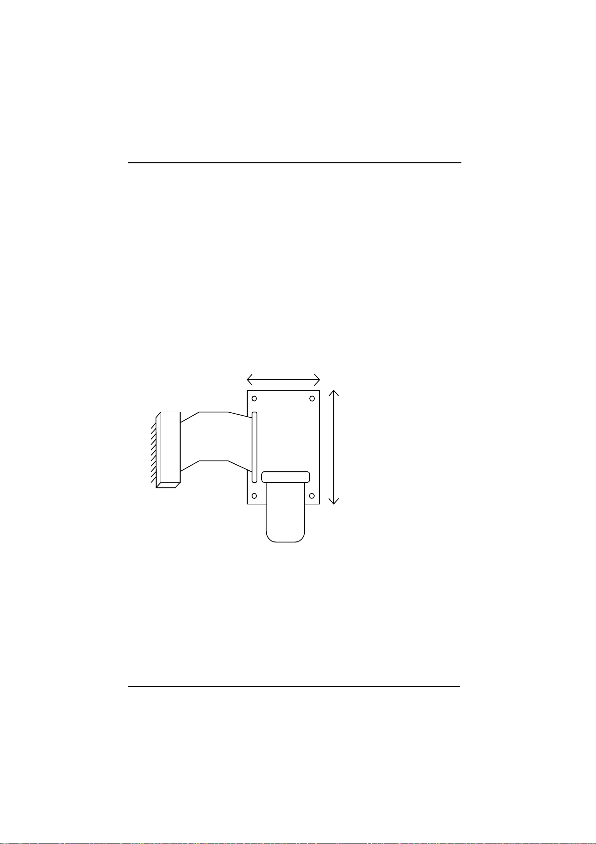
Page 76 Hardware Technical Section
5.22.5 Standard 32 Pin Flash Cards (Not PCMCIA)
A number of third party manufacturers are making credit card sized memory
cards usi ng th e TSOP type devices. Blue Chi p Techn ology has desig ned a card
socket PCB which will allow one card to be accessed by the on-board 32 pin
Flash DIL socket.
The standard card size is 1 MByte. The part number for the Memory Card
Socket is 971-185.
Once you have added extra Fla sh memor y to the un it , p lease see th e SSD section
of the Software Technical section to configure the APEX unit to access it.
The drawing that follows shows the basic principle:
Memory Card Diagram
102 m m
Ribbon Cable
32 way
Upto 450mm
32 Pin DIL Plug
Plugs into the FLASH IC Socket
Me mory c ard
PCB
107 m m
Card Socket
Memory
Card
The PCB has two sets of mounting holes. One set fits the standard 3½" floppy
disk drive mounting holes and th e other the standard PC104 mounting holes.
This allows the PCB to be used in many various ways. Please call Blue Chip
Technology for more information and pricing.
127-171.doc Blue Chip Technology Ltd.
Page 87

Hardware Technical Section Page 77
5.22.6 Adding SRAM
The APEX II unit can accommodate one 32 pin DIL integrated circuit (IC) via
its on-board SRAM DIL socket IC34.
This socket is located near to the EPROM IC, near the battery. If you have
ordered this unit with SRAM memory then is socket will be in use.
SRAM memory can be added as follows :
5.22.7 Standard 32 Pin SRAM DIL IC's
The use of conventional 32 pin DIL SRAM ICs. The following memory sizes
were available at the time of publishing:
128KByte
512KByte
Once you have added extra SRAM memory to the unit, please see the Software
Technical section to configure the APEX II unit to access it.
5.23 Using APEX II with a Host PC
Your desktop PC can be used as a programming tool or emulator to write
application specific programmes, debug them, and then transfer them to the
APEX II unit via a simple serial link.
This will allow you to develop your software in a known environment and take
advantage of existing PC software. Then with little effort you can program the
APEX II unit and see your application work.
For more detailed information on this topic please see the Flash programming,
Appendix I at the rear of this manual.
Blue Chip Technology Ltd. 127-171.doc
Page 88
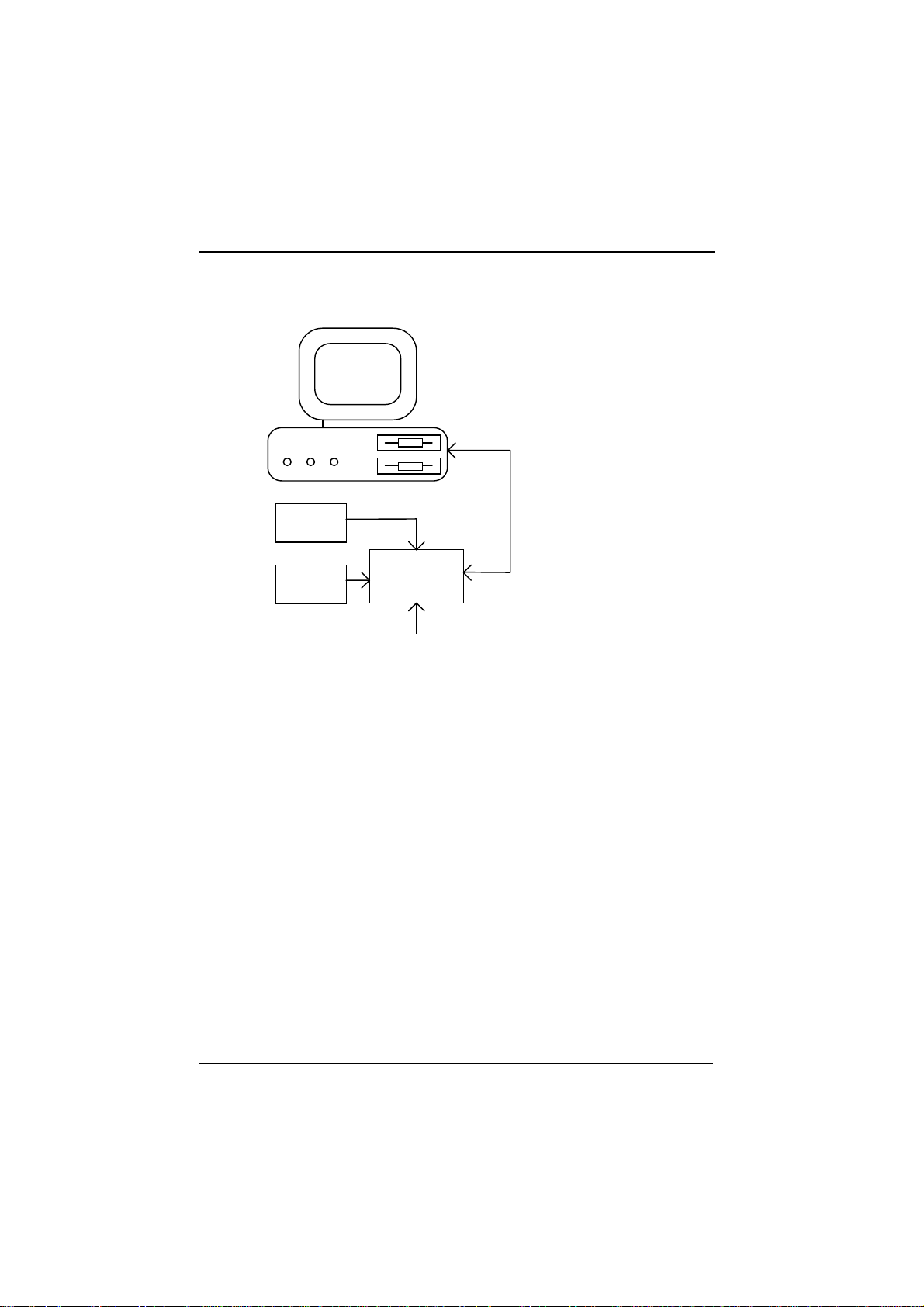
Page 78 Hardware Technical Section
g
p
prog
A basic block diagram is shown below indicating the various links to the
APEX II unit:
Desk Top
I/O ResTurbo
Keyboard
Display
APEX unit runs s
PC
A
C
APEX II
Power Input
ecial Remote Disk
ram via the BIOS
PC runs Server Pro
which lets the APEX unit
access the P C 's A: drive
Com1
ram
Simpl e 3 wire
RS232 Serial Link.
Link Normally on
Com1 of the PC
to Com1 of the
APEX unit
127-171.doc Blue Chip Technology Ltd.
Page 89

Hardware Technical Section Page 79
This page is intentionally left blank.
Blue Chip Technology Ltd. 127-171.doc
Page 90

Page 80 Software Technical Section
6. SOFTWARE TECHNICAL SECTION
6.1 Introduction
This section covers all aspects of the APEX II's software systems and should be
read fully before attempting to alter any of the System BIOS used to control the
workings of this unit. It is possible to alter the state of the System BIOS so that
a st a r t boot i s not pos si bl e a n d although this is not a catastrophic problem it can
be very frustrating and time consuming to remedy.
6.2 BIOS Overviews
There are several types of Basic Input Output System (BIOS) in a PC system.
System BIOS
This controls the local electronics. It also provides the interface to the hardware
for the operating system.
Video BIOS
This controls the interface between the video hardware and the computer.
Keyboard BIOS
This controls the keyboard matrix operation and communicates with the PC.
Adapter BIOS
Adapter ROM BIOS’ that control specific hardware add ons.
Each BIOS plays an important part to the total correct working of the PC. Each
one of the BIOS types will now be described in more detail.
6.2.1 System BIOS
The primary function of the System BIOS is to provide a series of software
interrupts, functions and sub-functions that perform specific system tasks; such
as writing or reading to and from disks and video screens.
127-171.doc Blue Chip Technology Ltd.
Page 91

Software Technical Section Page 81
The operating system uses the System BIOS as the route to communicate and
control the microprocessor and its immediate peripherals. This exchange of data
occurs via a strict protocol.
The secondary function of the System BIOS is the series of tests and
initialisations that occur after power-on. The results of these operations are
written to the POST display (not fitted as standard) as they are completed,
thereby indicating its progress.
The System BIOS on the APEX is contained in a 128KB EPROM; of this space
the System BIOS occupies 64KB. The EPROM is located at address F0000 Hex
and conti nues to FFFFF Hex. Th e supplier of th e BIOS is AMI, cur r entl y one of
the leading suppliers of PC BIOS in the world. Blue Chip Technology have
selected this supplier because of their experience, support and commitment to
future developments in this critical area of a PC/AT design.
For more information about AMI and there BIOS support software please
contact our Technical Support department who will be able to answer any
questions you may have.
At Blue Chip Technology we can also offer a BIOS customisation service which
will tailor the BIOS configuration to your applications needs.
This is normally free of charge with orders over 50 pieces. Plea se contact t he
Sales department for more information.
6.2.2 Video BIOS
The Video BIOS acts as an interface between the System BIOS and the video
hardware and sits at memory location C0000-C7FFFF. It is critical that this
interface is compatible, fast and reliable. The Video BIOS provides a relatively
high level of access to the hardware.
APEX II provides an on-board video interface and is based on the Cirrus
Logic™ CL-GD6235 IC. This device offers proven VGA compatibility in a
single device and is supported by 512KB of on board video memory (DRAM).
The Video BIOS coexists in the System BIOS EPROM but locates in the address
range C0000 to C7FFF hex. This BIOS is enabled and disabled with J4.
Due to the nature of some types of display (EL in particular), custom versions of
this BIOS are needed to access these panels. Please contact Blue Chip
Blue Chip Technology Ltd. 127-171.doc
Page 92

Page 82 Software Technical Section
Technology Ltd or your supplier to ensure that your display is supported by the
BIOS.
127-171.doc Blue Chip Technology Ltd.
Page 93

Software Technical Section Page 83
6.2.3 Keyboard and PS/2 Mouse BIOS
The keyboard and mouse BIOS is contained in the Megakey 8742 keyboard
controller. This device provides a parallel interface to the microprocessor bus
allowing a bi-directional streams of data to be passed between the PC, keyboard
and mouse. In addition to the keyboard and mouse the BIOS handles several of
the switch and LED functions on the PC. As this BIOS is programmed into the
8742 it occupies none of the memory map. This new keyboard controller also
provides several Green power saving features.
6.2.4 Expansion Bus ROMs
APEX II and conventional PC hardware allow add-on cards to be inserted on the
AT expansion bus. If software is required to control the electronics on these
cards the supplier may choose to provide this software in the form of an
expansion ROM or adapter ROM. On power-up the PC, once initialised, checks
for the presence of ROMs within th e memory space of C8000 to DFFFF Hex. If
presen t th e code withi n the ROM is run and t he specifi c hard ware on t he car d
controlled accordingly. In addition, this software can then be used as the
interface to the electronics by the operating system; thereby acting as an
extension to the System BIOS for the new electronics.
6.3 AMI WinBIOS System BIOS User Features
Features included are as follows :
• Keyboard Speed Switching
• Memory Detection
• Password Support
• Autodetection of IDE Hard Drive Parameters
• Autodetection of Processor Type and Speed
• Autodetection of Memory Size and Type
• Customisation of the System
• User definable Hard Disk Types
• PS/2 Mouse Support
• Boot Sector Virus Support
• Local Peripheral Support
• Shadow RAM Support
• Keyboard Typematic Rate and Delay
• Num Lock Power-on Status
Blue Chip Technology Ltd. 127-171.doc
Page 94

Page 84 Software Technical Section
• Fast Gate A20 Support
6.3.1 AMI WinBIOS Hot Key
The AMI WinBIOS provides a hot key to create a reset. These key operations
are:
<Ctrl>,<Alt> and <DEL> Causes a Soft Reset
All keys should be pressed down together to operate the chosen function.
6.3.2 AMI BIOS Power-on Self Test (POST)
AMI WinBIOS provides all IBM standard POST rout ines as well as enh anced
AMI BIOS routines. All POST checkpoin t codes are written to the POST displa y
at I/O location 80 Hex (not fitted as standard but available as an option fitted to
connector P6).
Appendix G gives a complete list and a detailed description of all of the POST
error codes. To view these error codes you will need the APEX II POST display
adapter.
6.3.3 POST Error Messages and Beep Codes
If the BIOS cannot configure the video display controller it will communicate
the identification of fatal errors (except error code 8) via a series of beeps. These
errors will only occur during power-on tests. A full list of beep codes can be
found in appendix G.
6.3.4 Accessing the AMI Set-up Screens
The AMI BIOS Set-up is accessed by pressing the 'DEL' key on the keyboard
when the screen displays the message:
Hit <DEL> if you want to run Set-up
If you press the 'DEL' key too late, reset the unit and try again.
You can reset the unit by either switching the main input power off and on, or by
using the HOT KEYS :-
127-171.doc Blue Chip Technology Ltd.
Page 95

Software Technical Section Page 85
<Ctrl>,<Alt> and <DEL> pressing them together.
6.3.5 Controlling the AMI Set-up Screens
This version of the AMI BIOS is designed to be controlled with a mouse
installed onto the COM1 port (RS232). However, you can access all of the setup routines without a mouse by using an attached keyboard and the following
basic key inputs as detailed in section 3.6.
If your application does not have a locally attached keyboard or display, then you
will need to run the APEX REMOTE ACCESS TERMINAL software. A BIOS
setting allows the APEX II to send all VIDEO and KEYBOARD information via
a serial link to a host PC also running suitable software. In this mode the APEX
II unit can be completely configured remotely and thus removes the need to have
access to the APEX II board at all. This will allow encapsulated or very remote
applications to be configured with great ease.
Please contact Blue Chip Technology for further information.
6.3.6 AMI BIOS Keyboard Control Keys
The following keyboard keys can be used either with a mouse or instead of a
mouse.
ESC Escapes back one menu level and also to exit.
TAB and Let you move around the various functions to be changed.
SHIFT TAB Also used to jump from menu to menu.
ARROW keys Lets you move up and down the menu lists under change.
ENTER key Is used to enter your changes.
ALT + H Provides HELP at any point
ALT + Space Global Exit
Blue Chip Technology Ltd. 127-171.doc
Page 96
Page 86 Software Technical Section
p
6.4 AMI BIOS Main Set-up Screen
The AMI WinBIOS main set-up screen is divided into four parts:
SET-UP sections 6.5 - 6.8
UTILITIES section 6.9
SECURITY section 6.10
DEFAULTS section 6.11
They are shown on the main screen as follows :
AMI BIOS Set u p
(C) 1994, American Megetrends Inc.
SETUP UTILITIES
Standard Advanced Chipset Detect Master Detect Slave
Peripheral
SECU RI TY DEFAULTS
Password Anti-Virus Original Optimal Fail-Safe
Colour Set
Al t + H : Hel
These four main sections are sub-divided into several smaller groups which are
now dealt with in more detail in the following sections.
127-171.doc Blue Chip Technology Ltd.
Page 97

Software Technical Section Page 87
6.5 SET-UP Section
The SET-UP Screen allows the user to configure the standard PC system
components like disk drives, time/date etc.
6.5.1 Standard (CMOS) Set-up
Date/Time
Date
This entry allows you to set the Day, Date, Month and Year.
Time
This entry allows you to set the Hours, Minutes and Seconds. The clock operates
in 24 hour mode; that means for a p.m. time add 12 to the hour e.g. enter 6:35
PM as 18:35:00.
Floppy A and Floppy B Disk Configuration
The APEX II unit via the BIOS will support 2 floppy disk drives A: and B:. The
configuration list is as follows :
Not Installed
360KB 5¼"
720KB 5¼"
1.2MB 5¼"
1.44MB 3½"
2.88MB 3½"
Both disk drives can be selected and can have either the same or different
configurations.
Master Disk and Slave Disk Configuration
Two hard disk drives are supported directly by the BIOS these being C: and D:.
Each drive can be selected as either drive types 1 to 46, custom 47, ESDI or
SCSI. Custom type 47 (user) is user definable allowing all parameters for the
drive to be customised. Both drives can be set to a different type 47 if required.
Blue Chip Technology Ltd. 127-171.doc
Page 98

Page 88 Software Technical Section
When custom 47 option is selected and auto detect is accessed (via the Utilities
Set-up) the system will detect the hard disk parameters for hard disk drives
connected with IDE interfaces.
It then displays the parameters that it detects and allows you to accept or reject
the parameters. If accepted, these parameters are displayed for the hard disk
drive.
Please note that when Auto Detect is run on a drive that is not present (drive D:
in most systems), there will be a delay before the test is completed.
6.6 Advanced (CMOS) Set-up
The Advanced set-up screen allows you to customise various primary parts of the
BIOS. These are in order as follows :
6.6.1 Typematic Rate, Delay and Programming
The control of Typematic rate Programming allows the auto repeat and delay
before repeat to be selected. The defaults and options are as shown on the screen.
The Typematic Rate Delay describes the delay before auto repeat starts. The
Typematic Rate is the frequency of the key generation once in auto repeat.
6.6.2 System Keyboard
The APEX II keyboard interface is AT and PS/2 compatible, and can be
connected to either AT or PS/2 keyboards. The default setting is Enabled. If your
system is to operate without a keyboard then select Disabled. Failure to do this
will result in an error being generate during the power-on diagnostics check.
6.6.3 Primary Display
This entry allows the user to select between one of the following :
MDA, CGA or EGA/PGA/VGA display controllers.
If your system is to operate without a display then select Disabled. Failure to do
this will result in an error being generated during the power-on diagnostics
check.
127-171.doc Blue Chip Technology Ltd.
Page 99

Software Technical Section Page 89
6.6.4 Mouse Support
This enables or disables the mouse support option. Th e mouse control is effected
by the 8742 keyboard controller on the APEX II unit and is PS/2 compatible.
6.6.5 Above 1MB Memory Test
By enabling this test any RAM above 1MB will be exercised by the POST
dia gnost ics th ereby tak ing l onger to boot. I f your unit is not fitted with more
than 1MB of RAM or you wish to shorten the boot time, set this option to
disabled. If you wish to ensure maximum DRAM integrity then set this option
to Enabled.
6.6.6 Memory Test Tick Sound
This option selects whether an audible indication of the presence of memory
during the POST is generated or not. Once either <ESC> or <DEL> is
depressed the audio output is disabled.
6.6.7 Parity Error Check
This option selects whether the parity circuit is active on the system DRAM. We
strongly recommend that this is set to enabled at all times thereby providing
communication of any RAM corruption. If this option is not required select
disabled.
6.6.8 Hit "DEL" Message Display
Disabling this option removes this message prompt from appearing during
power-up. This may be required when you do not wish to draw attention to
existence of the Set-up Menus within the BIOS. The default is enabled.
6.6.9 Extended BIOS RAM Area
The system BIOS holds data in a BIOS table in an area of RAM set by this
function. The 2 settings are 0:300 or DOS 1K
The system default is 0:300.
Blue Chip Technology Ltd. 127-171.doc
Page 100

Page 90 Software Technical Section
6.6.10 Wait for "F1" If any Error
If any of the tests run dur in g th e POST cause an err or th en th is messa ge will be
displayed. If this message is enabled then after displaying it the DX1 will halt
waiting for <F1> to be pressed. If you expect errors during the POST or do n ot
wish the boot to be halted if any error occurs then disable this option.
6.6.11 System Boot Up Num Lock
If you wish the numeric keypad to be active after a boot then select ON. If,
however, you wish the ←,↑,↓ and → keys to be available after power-up then
set this option to OFF.
6.6.12 Floppy Drive Seek At Boot
If enabled, a seek is performed on floppy drive A: at system boot time. The
opti ons a re En able d or Di sable d. By dis ablin g th is op tion the boot time can be
reduced. If very old 360KB drives are used it may be necessary to enable this
option to ensure that the heads are recalibrated before any data is accessed.
6.6.13 Floppy Disk Swapping
This function allows the user to swap the floppy disk drives on his system. Two
floppy disk units on the system say A: = 3½" an d B: = 5¼" swapped would then
be the A: = 5¼" and the B: = 3½"
The options for this BIOS function are :
Enabled or Disabled.
The system default is disabled.
6.6.14 System Boot Up Sequence
Th e defa u l t boot seq ue n ce i s dr i ve A: a n d t h e n C :. T hi s wou ld m ea n t ha t if d r i ve
A: is not r eady then t he boot occurs fr om dri ve C:. The alternative is to boot
from drive C: and if C: is not ready then drive A. Hence the settings are either:
“A:, C:” or “C:, A:”.
127-171.doc Blue Chip Technology Ltd.
 Loading...