

Page 1

APEX 104 CPU
&
APEX 104 CI-2
User Manual
Page 2

APEX 104 CPU
&
APEX 104 CI-2
User Manual
Document Part N° 127-150
Document Reference APEX\..\127-150.DOC
Document Issue Level 2.0
Manual covers PCBs with the following Revision N° A
All rights reserved. No part of thi s publication may be repr oduced, stored in any retri eval system or
transmitted, in any form or by any means, electronic, mechanica l, photocopied, recorded or other wise,
without the pri or permi ssion, in wr iti ng, from t he pu bl isher . For permi ssion in the UK conta ct B l u e C hip
Technology.
Information offered in this ma nual i s correct at the time of printing. Blue Ch ip Technology a ccepts no
responsibility for any inaccuracies. This information is subject to change without notice.
All trademarks and registered names acknowledged.
Blue Chip Technology Limited
Chowley Oak, Tattenhall,
Chester, Cheshire
CH3 9EX
Telephone : 01829 772000 Facsimile : 01829 772001
Page 3

Amendment History
Issue
Level
Ci 07/03/95 PD Split and updated
2.0 14/12/95 BH Joined, EMC statement added,
Issue
Date
Author Amendment Details
Parallel port detection changed in
BIOS section
Page 4

APE X 104
Page
CONTENTS
INTRODUCTION .......................................................................................... 1
COMPANY PROFILE...................................................................................3
PREFACE.......................................................................................................4
THE PC AS AN EMBEDDED CONTROL SOLUTION..............................4
THE APEX PRODUCT RANGE...................................................................5
TYPICAL CONFIGURATIONS OF APEX MODULES..............................6
i
APEX 104 CPU & CI-2 S
APEX 104 CPU, CI-2 & SSD S
APEX 104 CPU O
UTLINE
.........................................................................6
TACK
................................................................6
TACK
.................................................................................7
STACKING AND EMBEDDING THE APEX SYSTEM.............................8
USING THE APEX WITH A DESKTOP PC................................................8
SPECIFICATION...........................................................................................9
O
N-BOARD FEATURES
M
EMORY OPTIONS
P
OWER REQUIREMENT (TYPICAL
E
NVIRONMENT
........................................................................................9
...........................................................................................10
).....................................................................10
................................................................................................10
BIOS..............................................................................................................11
I
NTRODUCTION
System BIOS
Video BIOS
Keyboard BIOS
Expansion ROMs
AMI H
I-FLEX SYSTEM
Features
Hot Keys
AMIBIOS Power-on Self Test
POST Error Messages and Beep Codes
................................................................................................11
..............................................................................................11
................................................................................................12
...........................................................................................13
........................................................................................13
BIOS ...........................................................................14
......................................................................................................14
.....................................................................................................14
.....................................................................15
.......................................................15
Blue Chip Technology 127-150
Page 5

APE X 104
ii
Page
AMIBIOS S
S
TANDARD
A
DVANCED
A
DVANCED CHIPSET SETUP
P
ERIPHERAL SETUP
U
TILITIES
R
UNNING THE
A
CCESSING SETUP
S
ETUP KEY USE
........................................................................................................ 16
Using the CMOS Setup Program
Date
............................................................................................................ 21
Time
........................................................................................................... 21
Floppy Disk Configuration
Hard Disk Configuration
Display
Keyboard
Using the Advanced CMOS Setup
Help Screens
Typematic Rate, Delay and Programming
Mouse Support Option
Above 1MB Memory Test
Memory Parity Error Check
Hit <DEL> Message Display
Hard Disk Type 47 RAM Area
Wait for <F1> If any Error
System Boot Up Num Lock
Floppy Drive Seek at Boot
System Boot Up Sequence
System Boot Up CPU Speed
Fast Gate A20 Option
Password Checking Option
ROM Shadow
Boot Sector Virus Protection
Using the Advanced Chipset
Low CPU Speed
Early Ready Mode
Bus Clock Speed Select
DMA Clock Select
Additional RAM Wait State
RAS Timeout Feature
Extended Boundary
............................................................................................ 16
ETUP
CMOS S
CMOS S
................................................................................ 16
ETUP
................................................................................ 16
ETUP
.............................................................................. 16
.......................................................................................... 16
AMIBIOS S
....................................................................... 17
ETUP
........................................................................................... 17
............................................................................................... 18
................................................................. 20
.......................................................................... 21
............................................................................. 21
....................................................................................................... 21
.................................................................................................... 21
............................................................... 22
............................................................................................... 23
................................................... 23
................................................................................ 23
........................................................................... 23
........................................................................ 23
....................................................................... 23
.................................................................... 24
.......................................................................... 24
......................................................................... 24
........................................................................... 24
........................................................................... 24
........................................................................ 25
................................................................................. 25
......................................................................... 25
............................................................................................. 25
....................................................................... 26
....................................................................... 26
.......................................................................................... 27
....................................................................................... 27
............................................................................... 27
...................................................................................... 27
........................................................................ 27
................................................................................. 27
..................................................................................... 28
Blue Chip Technology 127-150
Page 6

APE X 104
iii
Page
Global EMS
EMS I/O Port Access
EMS Page Register
Hidden Refresh
Refresh On Idle
AT Refresh Disable
Video BIOS Area Cache (32K)
F000 BIOS Area Cache (64K)
Using the Peripheral Setup
On-Board Floppy Drive
On-Board IDE Drive
First Serial Port Address
Second Serial Port Address
Auto Configuration with Defaults
Change Passwords
Bypassing Password Support
Enabling Password Support
If a Password is Used
Password Storage
Password Options Control Prompt
Using a Password
Auto Detect Hard Disk
Write to CMOS and Exit
Do Not Write to CMOS and Exit
W
ATCHDOG TIMER
E²PROM A
F
LASH ACCESS
O
N-BOARD SERIAL AND PARALLEL PORTS
S
ERIAL PORTS
P
ARALLEL PORT
B
ATTERY
B
ACKPLANE
M
EMORY MAP
................................................................................................29
..................................................................................29
.....................................................................................29
...........................................................................................29
...........................................................................................29
.....................................................................................29
...................................................................30
....................................................................30
..........................................................................31
..............................................................................31
...................................................................................32
.............................................................................32
.........................................................................32
...............................................................33
......................................................................................33
.......................................................................33
........................................................................33
..................................................................................33
........................................................................................34
..............................................................34
........................................................................................34
................................................................................34
............................................................................35
................................................................35
..........................................................................................37
............................................................................................38
CCESS
................................................................................................38
.........................................................39
.................................................................................................39
..............................................................................................39
........................................................................................................40
.....................................................................................................40
.................................................................................................42
Typical Memory Map for a 1MByte APEX CPU & CI 2
.............................42
Blue Chip Technology 127-150
Page 7

APE X 104
Page
APEX CONFIGURATION JUMPERS........................................................43
iv
P1: PC/104 8
P2: PC/104 16
P3: 3½" D
P4: P
ERIPHERAL
P5: B
ATTERY
P6: P
ARALLEL
P7: C
O-PROCESSOR
P8: S
ERIAL
P9: S
ERIAL
APEX B
I/O A
I
NTERRUPT ASSIGNMENTS
DMA A
POST E
W
A
F
W
FLASH F
E2 F
W
APEX U
R
F
US SIGNAL DESCRIPTIONS
DDRESS MAP
SSIGNMENTS
RROR CODES
IRING TO THE PERIPHERAL CONNECTOR
BIOS E
PEX
LASH MEMORY FUNCTIONS
FLASH S
RITE
ORMAT
UNCTIONS
ATCHDOG FACILITY
TILITIES
EMOTE DISK
LASH DISK
(64
BIT
BIT
ISK DRIVE
(20
(3
WAY HEADER
(26
WAY HEADER
1 RS232 (10
2 RS485 (10
........................................................................................... 56
XTENSIONS
ECTOR
............................................................................................. 64
................................................................................................ 65
............................................................................................. 68
.................................................................................................. 68
..................................................................................................... 71
) .............................................................................44
WAY
(40
) ...........................................................................45
WAY
(4
WAY HEADER
WAY HEADER
)..................................................................46
) ........................................................................46
).....................................................................47
(36
WAY HEADER
WAY HEADER
WAY HEADER
................................................................................ 57
........................................................................................ 57
....................................................................................... 58
................................................................................. 62
............................................................................ 63
................................................................................... 64
...................................................................................... 66
)..............................................................45
).............................................................47
)............................................................48
)............................................................48
................................................................... 49
......................................................... 61
APEX CI-2....................................................................................................73
I
NTRODUCTION
................................................................................................ 73
SPECIFICATION......................................................................................... 73
O
N-BOARD FEATURES
V
............................................................................................................. 74
IDEO
S
ERIAL PORTS
D
IGITAL
D
ISK DRIVES
F
LOPPY
H
(IDE) D
ARD
H
ARD DISK TYPES
Blue Chip Technology 127-150
.................................................................................................. 74
PIO...................................................................................................75
................................................................................................... 75
........................................................................................................... 75
...................................................................................... 73
.......................................................................................... 76
RIVE
........................................................................................... 76
Page 8

APE X 104
Page
APEX-CI 2 CONFIGURATION JUMPERS...............................................79
APEX-CI 2 CONNECTOR PIN-OUTS .......................................................80
v
P1: PC/104 8
P2: PC/104 16
P3: RS422/485 S
P4: LCD I
P5: IDE/H
P6: D
IGITAL
P7: V
IDEO
P8: S
ERIAL
P9: F
LOPPY
P10: S
ERIAL
P11: IDE A
I/O A
DDRESS MAP
APEX 104-CI 2 E
I
NTERRUPT ASSIGNMENTS
DMA A
SSIGNMENTS
(64
BIT
BIT
ERIAL
NTERFACE
ARD DRIVE
I/O P
ORT
(10
WAY HEADER
1 (10
WAY HEADER
(34
WAY HEADER
2 (10
WAY HEADER
CTIVITY
...........................................................................................86
XTENDED
).............................................................................80
WAY
(40
)...........................................................................81
WAY
(10
WAY HEADER
(40
WAY SOCKET
(40
WAY HEADER
(26
WAY HEADER
)........................................................81
)............................................................82
)..........................................................83
).........................................................83
)...........................................................................84
).......................................................................84
).........................................................................84
).....................................................................85
LED (2
WAY HEADER
I/O P
ORT MAP
)......................................................85
......................................................87
................................................................................88
.......................................................................................88
APPENDIX A - USING THE DIGITAL PIO..............................................89
Electrical Options
G
ENERAL
PIO G
TTL R
LOSSARY
.......................................................................................91
EQUIREMENT
..........................................................................98
...............................................................................................99
APPENDIX B - CONNECTING TO DISPLAYS & PERIPHERALS......100
C
ONNECTING TO THE
V
IDEO OUTPUTS
CRT
DISPLAY HEADER
............................................................................................102
..................................................100
CRT DISPLAY TYPES..............................................................................103
IBM S
TANDARD VIDEO MODES
C
IRRUS LOGIC EXTENDED VIDEO MODES
V
IDEO DRIVERS
.............................................................................................104
.....................................................................103
.......................................................103
ELECTROMAGNETIC COMPATIBILITY (EMC) ...............................115
Blue Chip Technology 127-150
Page 9

APE X 104
Page
1
Introduction
This manual describes the Blue Chip Technology APEX processor card. There
are several versions of the card; these will be identified separately where
appropriate. We strongly recommend that you study this manual carefully before
attempting to change the configuration. Whilst all necessary information is
available in this manual we would recommend that unless you are confident, you
contact your supplier to effect any changes. Please be aware that it is possible to
create configurations that make booting impossible. If this should happen
disconnect the battery for approximately two hours, then reconnect the battery
and on power-up the default values will be written into the CMOS. Thi s product
uses the Chips & Technologies 82C836 VLSI device, this provides a complete
AT compatible environment. For further detailed information on this device
please call your supplier.
WARNING
The devices on this card can be fatally damaged by static electricity. Ensure that
you touch a suitable
ground
card. This should be repeated if the handling is for any length of time.
to discharge any static build up before touching the
If this product proves to be defective, Blue Chip Technology is only obliged to
replace or refund the purchase price at Blue Chip Technology's discretion
according to the accompanying terms and conditions of the registration card.
Blue Chip Technology 127-150
Page 10

APE X 104
Page
Limitations of Liability
In no event shall Blue Chip Technology be held liable for any loss, expenses or
damages of any kind whatsoever, whether direct, indirect, incidental or
consequential, arising from the design or use of this product or the support
materials supplied with this product.
Trademarks
IBM, PC, AT and PS/2 are trademarks of International Business Machines
Corporation.
AMI Hi-Flex BIOS is a trademark of American Megatrends Inc.
Intel is a registered trademark of Intel Corporation
80386SX is a registered trademark of Intel Corporation
CX486SLC is a registered trademark of Cyrix Corporation
2
Blue Chip Technology 127-150
Page 11

APE X 104
Page
3
Company Profile
Blue Chip Technology is based in the North West, the purpose built 15,000 sq ft
complex contains our research & development facility, engineering workshop,
conventional & SMT production lines.
Specialising in the provision of industrial computing and electronic solutions for
a wide range of UK and European organisations we have one of the UK's largest
portfolios of industrial PC's, peripherals and data acquisition cards. This
exten sive ran ge of products coupl ed with our experien ce and exper tise ena bles
Blue Chip Technology to offer an industrial processing solution for any
application. APEX is the latest addition to our portfolio, providing a cost
effective product development and volume production tool for OEMs.
A unique customisation and specialised system integration service is also
available, delivering innovative solutions to customers problems. The company's
success and reputation in this area has lead to a number of large design and
manufacturing projects for companies such as BNFL, Aston Martin, Jaguar
Sport and British Gas.
British Standards Institute approval (
BS5750 Part1, ISO 9001
) means that all
of Blue Chip Technology's design and manufacturing procedures are strictly
controlled, ensuring the highest levels of quality, reliability and performance.
Blue Chip Technology are committed to the single European market and
continue to invest in the latest technology and skills to provide high performance
computer and electronic solutions.
Blue Chip Technology 127-150
Page 12

APE X 104
Page
Preface
The PC as an Embedded Control Solution
As today's OEMs battle to develop leading edge products as fast as possible with
minimal cost, the APEX embeded PC system provides a innovative solution.
Designed to provide a high performance, compact hardware solution with
maximum configuration compatibility and flexibility, APEX is essentially a
range of modular building blocks wich allow OEMs to embedd microprocessor
control into a wide range of products.
Traditional methods of embedding computer control into products are being
challenged by the latest developments in embedded PC technology. This has
resulted in a dramatic increase in the number of applications which are using
PC as an embedded control solution.
Until recently, the only options were expensive and bulky bus board products
such as VME or STE or the resource hungry solution of designing a
microcontroller from scratch. By using the APEX processor as a "drop-in"
alternative, OEMs can gain clear cut advantages in design, production and
product enhancement.
4
PC is the best understood hardware interface in the world
•
Because the PC is a complete subsystem, design effort is minimised
•
Resource can be focused on the application specific features of the
•
target product
Development resource is reduced, saving time and money
•
Access to PC application software enhances product functionality
•
A large pool of engineering and programming talent reduces
•
development times
User familiarity with DOS and Windows interfaces enhances product
•
attractiveness
Low cost and well understood development tools reduce personnel
•
learning curves
An off the shelf solution reduces material needs and costs
•
Reduced time to market maximises sales and optimises profit window
•
Blue Chip Technology 127-150
Page 13

APE X 104
Page
The APEX Product Range
The APEX range consists of a processor base and a series of Functional Support
Modules which allow highly integrated control systems can be built. All of the
products in the range can be plugged into an OEM circuit board, connected via
the AT stackthrough bus or plugged into a standard passive
backplane.
Summary of Product Range
APX-3S/4SL Processor
Functional Support Modules
APX-CI 2 General interface controller
Other Functional Support Modules
A range of functional support modules have also been designed. Measuring
90mm by 96mm, they provide a wide range of interfaces to the outside world.
5
Blue Chip Technology are one of the UK's leading manufacturers of data
acquisition and specialised I/O cards. Our unique design and manufacturing
capabilities, enable us to provide a customised embedded processing solution,
providing you with a range of FSM's tailor made for your needs.
Blue Chip Technology 127-150
Page 14
APE X 104
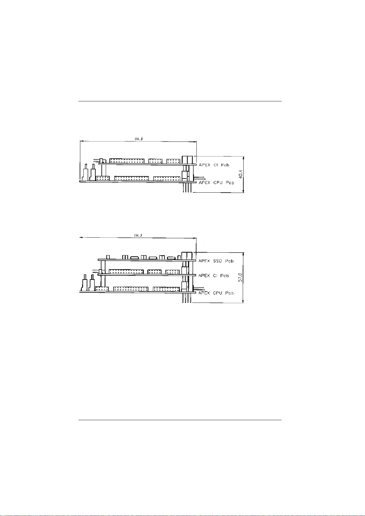
Typical Configurations of APEX Modules
APEX 104 CPU & CI-2 Stack
APEX 104 CPU, CI-2 & SSD Stack
Page
6
Blue Chip Technology 127-150
Page 15
APE X 104
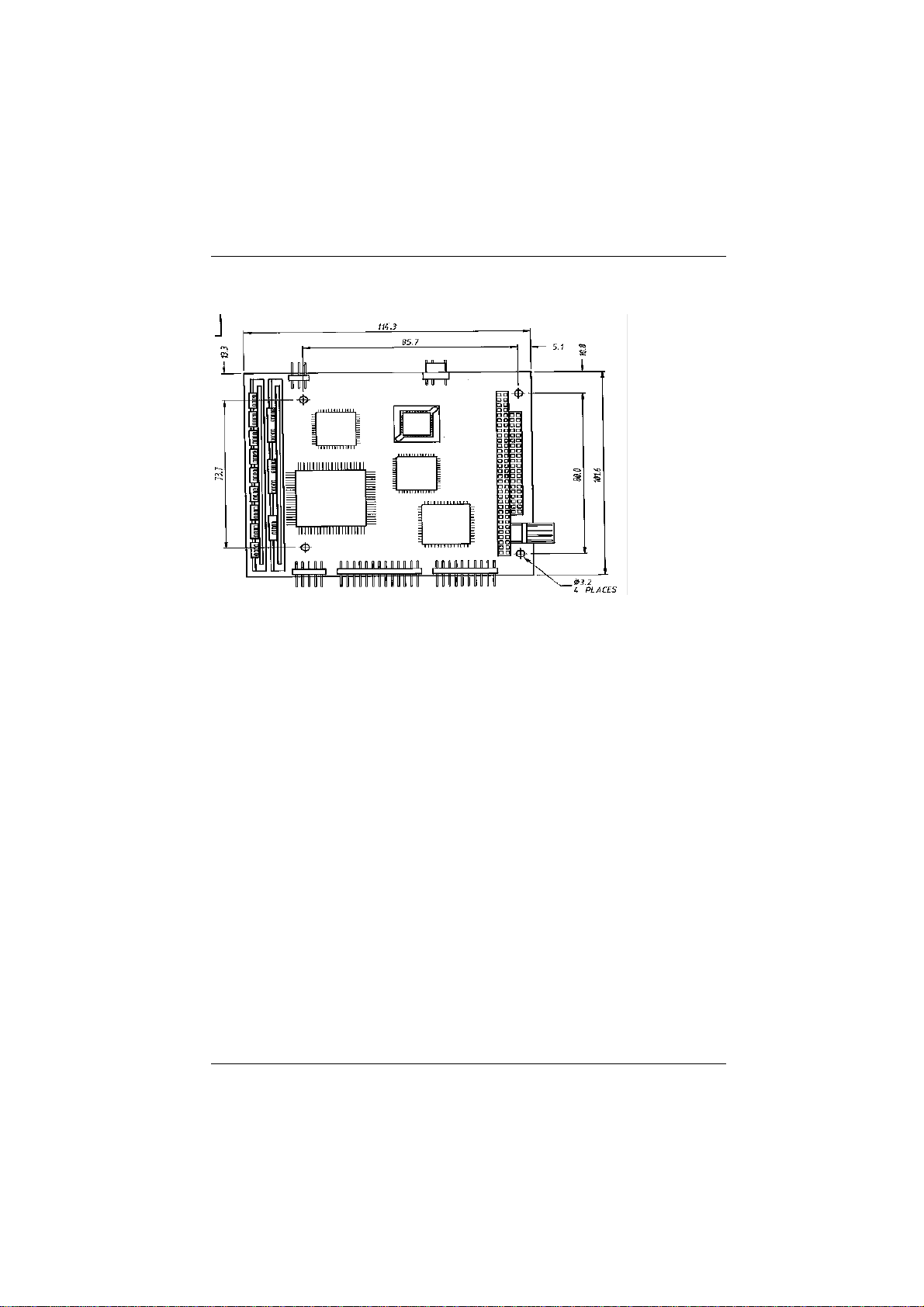
APEX 104 CPU Outline
Page
7
Blue Chip Technology 127-150
Page 16

APE X 104
Page
8
Stacking and Embedding the APEX System
Where space and complexity rule out a passive backplane or card cage, APEX
modules can be stacked on top of each other to form the complete subsystem.
The example below shows how a unit can be configured to allow a fully
functiona l PC with VGA, IDE , 2 4 ch an n els of progr ammable I/O and solid state
disk capability, to be achieved in a form factor of (100mm x 114mm x 48mm).
This allows the APEX to be used as a standalone development tool. By adding a
keyboard and monitor, you have a complete PC system which will function
exactly the same as your desktop PC.
APEX can also be plugged into a custom built electronic assembly, allowing you
to add microprocessor control to any application specific electronic design.
Further functionality can be designed in by adding FSM's as required.
Using the APEX with a Desktop PC
Your desktop PC can be used as a programming tool or emulator to write
application specific programmes, debug them, then transfer them to APEX
processor. An adapter ca rd (APX-PC) allows all APEX products to be plugged
into a standard passive backplane for this purpose. This allows you to develop
your software in a known environment and take advantage of existing PC
software.
Blue Chip Technology 127-150
Page 17

APE X 104
Page
Specification
The Blue Chip Technology APEX embedded PC is an ultra compact high
performance computer that provides 100% IBM PC/AT compatibility.
On-board Features
Choice of 25 MHz 80386SX 80486sSLC or 80486SLC2 50MHz
•
microprocessor
80387SX coprocessor support (optional)
•
Up to 8MB of DRAM memory, supports 256K x 9, 1MB x 9, and 4MB x 9
•
SIMM modules.
High performance memory Page Interleave access
•
Up to 1MB on board FLASH
•
AMI BIOS with built in setup program
•
Hardware EMS support (LIM 3.2 & 4.0 compatible)
•
PC/104 Compatible
•
Selectable Shadow RAM for system & video BIOS
•
Selectable Bus speed
•
Automatic or Manual Peripheral Configuration.
•
2 Asynchronous serial ports (16C450 compatible) with LC filters - 1 RS232
•
& 1 RS485
Uni-directional parallel port
•
AT compatible keyboard port
•
PS/2 Mouse port
•
Customer "sign-on" information held in EEPROM (64 bytes available for
•
user operation)
Software selectable Watchdog timer
•
On-board "Power Good" generation
•
Speaker drive circuitry
•
5 Volt only operation
•
6 layer PCB with Surface Mount Technology (SMT)
•
9
Blue Chip Technology 127-150
Page 18

APE X 104
Memory Options
Option SIMM1 SIMM2 Total DRAM
1 256KB 256KB 512KB
2 1MB 1MB 2MB
3 4MB 4MB 8MB
Note:
Bank 0 is made up of two 30 pin standard SIMM carriers.
•
All SIMMs must have an access time of 70ns or faster (e.g 60ns).
•
Three chip SIMMs are prefered because of their lower power consumption.
•
All SIMMs with in a Ban k
•
be the same, you
must
mix 256KB, 1MB
cannot
and 4MB within the same Bank.
JP4 selectes between option 1&2 or 3
•
Power Requirement (typical)
Configuration Current @ 5V
APEX 386SX @ 25MHz with 8MBytes of DRAM 1.2 Amperes
APEX 486SLC @ 25MHz with 8MBytes of DRAM 1.3 Amperes
APEX 386SX @ 25MHz with 8MBytes of DRAM + CI 1.6 Amperes
APEX 486SLC @ 25MHz with 8MBytes of DRAM + CI 1.8 Amperes
APEX 486SLC2 @ 50mhz with 8mbytes of DRAM + CI 2.0 Amperes
Page
10
Environment
Operating Temperature 0°C to 60°C.
Storage Temperature -20°C to 70°C.
Relative Humidity 10-90% non-condensing.
Blue Chip Technology 127-150
Page 19

APE X 104
Page
11
BIOS
Introduction
There are several types of Basic Input Output Systems (BIOS) in a PC system.
System BIOS
This controls the local electronics. It also provides the interface to the hardware
for the operating system.
Video BIOS
This controls the interface between the video hardware and the computer.
Keyboard BIOS
This controls the keyboard matrix operation and communicates with the PC.
Adapter
Adapter ROM BIOSes that control specific hardware add-ons.
Each of these BIOSes will now be described :
System BIOS
The primary function of the System BIOS is to provide a series of software
interrupts, functions and subfunctions that perform specific system tasks; such as
writing or reading to and from disks and video screens.
The operating system uses the System BIOS as the route to communicate and
control the microprocessor and its immediate peripherals. This exchange of data
occurs via a strict protocol .
The secondary function of the System BIOS is the series of tests and
initialisations that occur after power-on. The results of these operations are
written to the POST displ ay (not fitted) as they are completed, thereby indicating
its progress.
Blue Chip Technology 127-150
Page 20

APE X 104
Page
12
The System BIOS on the APEX is contained in a 128KB EPROM; of this space
the System BIOS occupies 64KB. The EPROM is located at address F0000 hex
and continues to FFFFF hex. The supplier of the BIOS is AMI, currently the
leadin g supplier of PC BIOSes in th e world. BLUE CHIP TECHNOLOGY ha ve
selected this supplier because of their experience, support and committment to
future developments in this critical area of a PC/AT design.
Video BIOS
The Video BIOS acts as an interface between the System BIOS and the video
hardware. It is critical that this interface is compatible, fast and reliable. The
Video BIOS provides a relatively high level of access to the hardware. The
companion APEX-CI 2 provides a video interface and is based on the Cirrus
Logic 6235. This device offers proven VGA compatibility in a single device and
is able to drive both CRT & LCD displays simultaneously. It is supported by a
512KB of video memory. The Video BIOS coexists in the System BIOS EPROM
and locates in the address range C0000 to C7FFF hex. Th is BIOS is ena bled and
disabled with J2 on the APEX CPU board(fit to disable).
Blue Chip Technology 127-150
Page 21

APE X 104
Page
13
Keyboard BIOS
The Keyboard BIOS is contained in the 8042 (or 8742) keyboard controller. This
device provides a parallel interface to the microprocessor bus allowing a bidirectional streams of data to be passed between the PC and the keyboard. In
addition the Keyboard BIOS handles several of the switch and LED functions on
the PC. The BIOS is programmed into the 8042. It occupies none of the memory
map.
Expansion ROMs
APEX and conventional PC hardware allow add-on cards to be inserted on the
expansion bus. If software is required to control the electronics on the card the
supplier may choose to provide this software in the form of an expansion ROM
or adapter ROM. On power-up the PC, once initialised, checks for the presence
of ROMs within the memory space of C8000 to DFFFF hex. If present th e code
within the ROM is run and the specific hardware on the card controlled
accordingly. In addition this software can then be used as the interface to the
electronics by the operating system; therby acting as an extension to the System
BIOS for the new electronics.
Blue Chip Technology 127-150
Page 22

APE X 104
Page
14
AMI Hi-Flex System BIOS
Features
Keyboard Speed Switching
•
Memory Detection
•
Password Support
•
Autodetection of IDE Hard Drive Parameters
•
Autodetection of Processor Type and Speed
•
Autodetection of Memory Size and Type
•
Customisation of the System
•
User definable Hard Disk Types
•
PS/2 Mouse Support
•
Boot Sector Virus Support
•
Local Peripheral Support
•
Shadow RAM Support
•
Keyboard Typematic Rate and Delay
•
Num Lock Power-on Status
•
Fast Gate A20 Support
•
Hot Keys
The Hi-Flex AMIBIOS provides hot keys to switch speed and cache operation.
These key operations are:
<Ctrl>,<Alt> and <+> Selects High Speed
<Ctrl>,<Alt> and <-> Selects Low Speed
<Ctrl>,<Alt>,<Shift> and <+> Enables External Cache
<Ctrl>,<Alt>,<Shift> and <-> Disables External Cache
<Ctrl>,<Alt> and <DEL> Causes a Soft Reset
All keys should be pressed down together.
Blue Chip Technology 127-150
Page 23

APE X 104
Page
15
AMIBIOS Power-on Self Test
The Hi-Flex AMIBIOS provides all IBM standard POST routines as well as
enhanced AMIBIOS routines. All POST checkpoint codes are written to the
POST displa y at I/ O location 80 hex (not fitted). See the POST err or codes on
page 58 for detailed checkpoint codes.
POST Error Messages and Beep Codes
If the BIOS cannot configure the display controller it will communicate the
identification of fatal errors (except error code 8) via a series of beeps. These
errors will only occur during power-on tests. The beep codes are as follows:
Beeps Error Messages Description
1 Refresh Failure Memory Refresh circuitry faulty.
2 Parity Error Parity error in the first 64KB of
3 Base 64KB Memory Failure. Memory failure in the first 64KB.
4 Timer not Operational. Timer 1 is not functioning.
5 Processor error. CPU error.
6 8042 - Gate A20 Failure. BIOS cannot switch to protected
7 Processor Exception Interrupt
Error.
8 Display Memory Read/Write
Error.
9 ROM Checksum Error. ROM checksum embedded in the
10 CMOS Shutdown Register
Read/Write Error.
memory.
Alternatively, memory in the first
64KB faulty.
mode.
CPU generated an exception
interrupt
error.
Video adapter is not responding or
its memory is faulty.
ROM
does not match the calculated
value.
The shutdown register in the
CMOS RAM failed. Check access
to CMOS.
Blue Chip Technology 127-150
Page 24

APE X 104
Page
16
AMIBIOS Setup
The Hi-Flex AMIBIOS Setup utility is divided into five parts:
Standard CMOS Setup
The Hi-Flex AMIBIOS St an da r d CMOS Setu p per mits the user to configure and
set system components such as floppy drives, hard disk drives, time and date,
monitor type and keyboard. These options are discussed on page 20.
Advanced CMOS Setup
The Advanced CMOS Setup allows the user to configure more advanced parts of
memory operation and peripheral support. These options are discussed on page
22.
Advanced Chipset Setup
The Advanced Chipset configures the C&T SCATSX specific features and is
discussed further on page 26.
Peripheral Setup
The Peripheral Setup configures the APEX-CI 2 companion card's floppy, IDE,
serials and parallel devices. These are all controlled by the C&T 82C711 device.
These options are discussed further on page 31.
Utilities
The AMIBIOS provides support for Password security access. This will be
discussed further on page 33.
Blue Chip Technology 127-150
Page 25

APE X 104
Page
17
Running the AMIBIOS Setup
The system parameters (such as amount of memory,disk drives, video displays
and numeric coprocessors) a re stored in C MOS RAM. When the APE X i s t u rned
off, a back-up is provided by an external battery (3.7V Lithium) connected to P5.
Each time the APEX is powered-on, it is configured with these values, unless the
CMOS RAM has been corrupted. The AMIBIOS Setup resides in the ROM
BIOS and is available each time the APEX is switched on.
If, for some reason, the CMOS RAM becomes corrupted, the system is
reconfigured with the default values stored in the System BIOS. There are two
sets of BIOS values stored in the BIOS: the BIOS default values and the PowerOn default values.
Accessing Setup
Setup is accessed by pressing the ' DEL' key on the keyboard when the screen
displays the message:
Hit <DEL> if you want to run Setup
If you press 'DEL' too late, reset the APEX and try again.
Blue Chip Technology 127-150
Page 26

APE X 104
Page
18
Setup Key Use
Keystroke Action
Esc Returns to the previous screen.
→,←,↑ and ↓
<PgUp> and
<PgDn>,
<Ctrl><PgUp>,
<Ctrl><PgDn>
<F1> Displays help.
<F2> Changes background colours.
<F3> Changes foreground colours.
<F5> Restores the values resident when the current Setup session
<F6> Loads all features in the Advanced CMOS Setup/Advanced
<F7> Loads all features in the Advanced CMOS Setup/Advanced
<F10> Saves all the changes made to Setup and continues
Move the cursor from one option to the next.
Modify the default value of the options for the
highlighted parameter. If there are fewer than 10
options, <Ctrl><PgUp> and <Ctrl><PgDn> operate like
<PgUp> and <PgDn>.
<Ctrl> can also be used to increment a setting.
began. These values are taken from the CMOS RAM if it was
uncorrupted at the start of the session. Otherwise, the
AMIBIOS Setup default values are
used.
Chipset Setup with the AMIBIOS
Setup defaults.
Chipset with the Power-On defaults.
the boot process.
The APEX AMIBIOS Setup main Menu is shown below. The options are
selected by using the ↑ and ↓ keys and then pressing <Enter> .
AMIBIOS SETUP PROGRAM - BIOS SETUP UTILITIES
© Copyright 1992 American Megatrends, Inc. All Rights Reserved
STANDARD CMOS SETUP
ADVANCED CMOS SETUP
ADVANCED CHIP SET SETUP
AUTO CONFIGURATION WITH DEFAULTS
Standard CMOS Setup for changing time, Date, Hard Disk Type, etc.
Blue Chip Technology 127-150
PERIPHERAL SETUP
CHANGE PASSWORD
AUTO DETECT HARD DISK
WRITE TO CMOS AND EXIT
DO NOT WRITE TO CMOS AND EXIT
Page 27

APE X 104
Each option is described in detail on the pages identified as follows:
Main Menu Option Described on Page
Page
19
STANDARD CMOS SETUP
ADVANCED CMOS SETUP
ADVANCED CHIP SET SETUP
CI2 PERIPHERAL SETUP
AUTO CONFIGURATION WITH DEFAULTS
CHANGE PASSWORD
AUTO DETECT HARD DISK
WRITE TO CMOS AND EXIT
DO NOT WRITE TO CMOS AND EXIT
20
22
26
31
33
33
34
35
35
Blue Chip Technology 127-150
Page 28

APE X 104
Page
20
Using the CMOS Setup Program
The default condition for the CMOS Setup Menu is as sh own below. This men u
sets the basic system parameters, such as date, time, floppy disk and hard disk
types. By using the
←↑↓→
keys you can select the parameter to be changed.
Once positioned on the parameter to be modified the <PgUp> and <PgDn> keys
rotate the available options. The value selected when the menu is exited is the
one that will be written to CMOS, sh ould you decide to commit your changes to
CMOS.
AMIBIOS SETUP PROGRAM - CMOS SETUP PROGRAM
© Copyright 1992 American Megatrends, Inc. All Rights Reserved
Date (mm/date/year) Fri, Aug 07, 1992 Base memory 640 KB
Time (hour/min/sec) 09 : 38 : 09 Ext memory 0 KB
Cyln Head WPcom Lzone Sect Size
Hard disk C: type Not Installed
Hard disk D: type Not Installed
Floppy drive A: 1.44 MB, 3½
Floppy drive B: Not Installed
Primary Display VGA/PGA/EGA
Keyboard Installed
Esc = Exit ↑→↓←: Select F2: Colour PU/PD: Modify
Blue Chip Technology 127-150
Page 29

APE X 104
Page
21
Date
This entry allows you to set the Date, Month and Year. Ranges for each value
are shown in the lower left corner of the CMOS Setup Screen.
Time
This entry allows you to set the Hours, Minutes and Seconds. The clock operates
in 24 hour mode; that means that for a PM time add 12 to the hour e.g. enter
6:35 PM as 18:35:00.
Floppy Disk Configuration
The APEX supports None, 360KB, 720KB, 1.2MB, 1.44MB & 2.88MB drives.
Two drives are supported A: and B:.
Hard Disk Configuration
Two har d disk drives are supported directly by the BIOS C: and D:. E ach drive
can select drive types 1 to 46. In addition type 47 is user definable allowing all
parameters for the drive to be customised. Both drives can be set to a different
type 47 if required. To set the values for type 47 use the ←,↑,↓ and → keys to
select the appropriate field and then type in as required. A complete list of the 46
hard disk type is contained in the APEX-CI 2 manual.
Display
This entry allows the user to select MDA, CGA or EGA/PGA/VGA d isplay
controllers. If your system is to operate without a display then select Disabled.
Failure to do this will result in an error being generated during the power-on
diagnostics check.
Keyboard
The APEX keyboard interface is AT compatible. It can be connected to either
AT or PS/2 keyboards. The default setting is Enabled. If your system is to
operate without a keyboard then select Disabled. Failure to do this will result in
an error being generate during
Blue Chip Technology 127-150
the power-on diagnostics check.
Page 30

APE X 104
Page
22
Using the Advanced CMOS Setup
The default condition for the Advanced CMOS Setup Men u is as shown below.
By using th e
←↑↓→
keys you can select the parameter to be changed. Once
positioned on the parameter to be modified the <PgUp> and <PgDn> keys rotate
the available options. The value selected when the menu is exited is the one that
will be written to CMOS, should you decide to commit your changes to CMOS.
AMIBIOS SETUP PROGRAM - ADVANCED CMOS SETUP
Typematic Programming
© Copyright 1992 American Megatrends, Inc. All Rights Reserved
Typematic Rate Delay
Typematic Rate (Chars/sec)
Mouse Support Option
Above 1 MB Memory Test
Memory Parity Error Check
Hit <DEL> Message Display
Hard Disk Type 47 RAM Area
Wait for <F1> If Any Error
System Boot Up Num Lock
Floppy Drive Seek At Boot
System Boot Up Sequence
System Boot Up CPU Speed
Fast Gate A20 Option
Password Checking Option
:
Disabled
: 500
: 15.0
:
Disabled
: Enabled
: Enabled
: Enabled
: 0:300h
: Enabled
: On
: Enabled
: A:, C:
: High
: Enabled
:
Enabled:
Video ROM Shadow C000, 32K : Enabled
Adaptor ROM Shadow C800, 16K : Disabled
Adaptor ROM Shadow D000, 16K : Disabled
Adaptor ROM Shadow D800, 16K : Disabled
Adaptor ROM Shadow E000, 16K : Disabled
Adaptor ROM Shadow E800, 16K : Disabled
System ROM Shadow F000, 64K : Enabled
Boot Sector Virus Protection : Disabled
Esc = Exit
F5: Old Values F6: BIOS Setup Defaults F7: Power-on Defaults
↑→↓←
: Select (Ctrl) Pu/Pd: Modify F1: Help F2: Colour
Blue Chip Technology 127-150
Page 31

APE X 104
Page
23
Help Screens
Help can be invoked at any time by pressing <F1>.
Typematic Rate, Delay and Programming
The control of Typematic rate Programming allows the auto repeat and delay
before r epeat to be select ed. The defaults are a s shown a bove. The Typematic
Rate Delay describes the delay before auto repeat starts. The Typematic Rate is
the frequency of the key generation once in auto repeat.
Mouse Support Option
This enables or disables the mouse support. Th e mouse control is effected by the
8042 keyboard controller on the APEX. It is PS/2 compatible.
Above 1MB Memory Test
By enabling this test any RAM above 1MB will be exercised by the POST
dia gn ost ic s th er eby ta ki n g l ong er to boot . I f your APE X is n ot fitted with more
than 1MB of RAM or you wish to shorten the boot time set this option to
disabled.
Memory Parity Error Check
This option selects whether the parity circuit is active on th e system RAM. We
strongly recommend that this is set to enabled at all times thereby providing
communication of any RAM corruption. If this option is not required select
disabled.
Hit <DEL> Message Display
Disabling this option removes this message from appearing during power-up.
This may be required when you do not wish to draw attention to existence of the
Setup Menus within the BIOS. The default is enabled.
Blue Chip Technology 127-150
Page 32

APE X 104
Page
24
Hard Disk Type 47 RAM Area
As described in the CMOS Set up details previously the AMIBIOS supports type
47 user definable input. This data is stored at either:
0:300h in lower system RAM
or
Top 1KB of applications memory
The information will be stored in shadow RAM if shadowing is enabled.
Wait for <F1> If any Error
If any of the tests run dur in g th e POST cause an err or th en th is messa ge will be
displayed. If this message is enabled then after displaying it the APEX will halt
waiting for <F1> to be pressed. If you expect errors during the POST or do n ot
wish the boot to be halted if any error occurs then disable this option.
System Boot Up Num Lock
If you wish the numeric keypad to be active after a boot then select ON. If,
however, you wish the ←,↑,↓ and → keys instead after power-up then set the
option to OFF.
Floppy Drive Seek at Boot
If enabled, a seek is performed on floppy drive A: at system boot time. The
opti ons a re En able d or Di sable d. By dis ablin g th is op tion the boot time can be
reduced. If very old 360KB drives are used it may be necessary to enable this
option to ensure that the heads are recalibrated before the drive is accessed.
System Boot Up Sequence
Th e defa u l t boot seq ue n ce i s dr i ve A: a n d t h e n C :. T his wou l d m ea n th a t i f d r i ve
A: is not ready then the boot occurs from C:. T he alternative is to boot from
drive C: and then A: if C: is not ready. Hence the settings are either: A:, C: or
C:, A:.
Blue Chip Technology 127-150
Page 33

APE X 104
Page
25
System Boot Up CPU Speed
The Setup allows the selection of the CPU at boot time. The default is High
speed. The alternative is Low.
Fast Gate A20 Option
Gat e A20 con trols the me thod of a ccessin g memor y addr esses above 1 MB by
enabling or disabling access to the processor line A20. To provide XT
compatibility address line A20 must always be low and therefore the option
should be Disabled. However, some applications both enter protected mode and
shut down through the BIOS. For this software, Gate A20 must be constantly
enabled and disabled via the keyboard controller (8042), which slows down the
processing.
Fast Gate A20 is another method for handling Gate A20 using the SCATsx
internal circuitry. It speeds programs that constantly change from addressing
conven tional memory to addressing memory addresses above 1MB (from real
mode to protected mode and back). Network operating systems in particular
benefit from this enhanced circuitry.
The Default is Fast Gate A20 enabled.
Password Checking Option
This option enables a password check every time the systems boots or Setu p is
executed. The settings are Always or Setup. If Always is selected the user
password prompt appears every time the system is turned on. If Setup (the
default) is chosen, the password prompt appears if Setup is executed.
ROM Shadow
ROM shadow is a technique in which the BIOS code is copied from slower ROM
to faster RAM. The BIOS is then executed from the RAM.
For each of the areas of memory identified in the Setup table the option is there
to Enable or Disable shadowing for that particular area. The default is that both
the Vi deo and System ar eas ar e sh ad owed. Car e mu st be ta ken wher e expa nsi on
cards are occupying an area that is set for shadowing. If the expansion card h as
its own internal RAM located at the address that is shadowed then its operation
Blue Chip Technology 127-150
Page 34

APE X 104
Page
26
will be corrupted (examples are network cards). For such cards the setting
should be Disabled.
Boot Sector Virus Protection
When enabled, the BIOS issues a warning when any program or Virus issues a
Disk Format command or attempts to write to the boot se ctor of t he h ard disk .
The settings are Enabled or Disabled.
Using the Advanced Chipset
The default condition for the Advanced Chipset Setup Menu is as shown below.
By using th e
←↑↓→
keys you can select the parameter to be changed. Once
positioned on the parameter to be modified the <PgUp> and <PgDn> keys rotate
the available options. The value selected when the menu is exited is the one that
will be written to CMOS, should you decide to commit your changes to CMOS.
AMIBIOS SETUP PROGRAM - ADVANCED CHIPSET SETUP
© Copyright 1992 American Megatrends, Inc. All Rights Reserved
Low CPU Speed
Early Ready Mode
Bus Clock Speed Select
DMA Clock Select
Coprocessor Ready Control
Additional RAM Wait State
RAS Timeout Feature
Video Controller
Extended Boundary
Global EMS
EMS I/O Port Access
EMS Page Register
Hidden Refresh
Refresh On Idle
AT Refresh Disable
Video BIOS Area Cache (32K)
F000 BIOS Area Cache (64K)
: CXIN/4
: Enabled
: CXIN/4
: B/2
: 82C836
: Enabled
: Disabled
: Internal
: None
: Disabled
: Enabled
: EMS0
: Disabled
: Disabled
: No
: Disabled
: Disabled
Esc = Exit
F5: Old Values F6: BIOS Setup Defaults F7: Power-on Defaults
↑→↓←
: Select (Ctrl) Pu/Pd: Modify F1: Help F2: Colour
Blue Chip Technology 127-150
Page 35

APE X 104
Page
27
Low CPU Speed
Selects the fraction of the main oscillator frequency to be used for the Low CPU
speed. Default is CXIN/4 which for a 25MHz APEX would be: 50MHz / 4 =
12.5mhz operation.
Early Ready Mode
When enabled allows external devices to assert READY durin g t h e first T2 after
T1 state to terminate the memory cycle after only two T-states. The default is
Enabled.
Bus Clock Speed Select
The actual Bus Clock Speed is set by this option. The AT standard is 8MHz. We
advise a frequency as close to this as possible. However, for applications where
the ot her ca rds on t he backpl ane ar e capable of work ing at a hig her sp eed thi s
option is available. The formula is: CXIN (twice the processor speed) / the
setting.
Therefore for a 25MHz APEX: 50MHz / 6 (default) = 8.33MHz.
DMA Clock Select
The speed of the DMA clock is set by this option . The options ar e Bus Clock
Speed (see above) or Bus Clock Sp eed/2 . We r ecommen d th at B/ 2 is s et un less
you are sure that your additional cards can operate at the full bus speed.
Additional RAM Wait State
The Setup allows the RAM to operate with either 0 or 1 wait state. The default is
1 wait state. For improved performance this can be reduced to 0 wait state.
RAS Timeout Feature
This option is provided to support DRAM that allow a maximum RAS active
time of 10 microseconds. If the timeout is Enabled the RAS is not allowed to
remain low for more than 9.5 microseconds. With this option disabled the
maximum RAS active time is about 15 microseconds, limited by the refresh
cycle time.The default setting is Disabled.
Blue Chip Technology 127-150
Page 36

APE X 104
Page
28
Extended Boundary
This option defines the upper limit of available memory. The options are:
No Limit, 1MB, 1.25MB, 1.5MB, 2MB, 3MB, 4MB, 5MB, 7MB, 8MB, 9MB,
10MB, 11MB, 12MB, 13MB, 15MB.
Blue Chip Technology 127-150
Page 37

APE X 104
Page
29
Global EMS
This option is used to select whether the EMS hardware is to be operational. If
the setting is Disabled then the following EMS setting is ignored. The default is
Disabled.
EMS I/O Port Access
This setting again enables or disables the use of the EMS memory. If you wish to
use EMS select enabled. This is the default.
EMS Page Register
The EMS registers are accessed using three I/O ports. These ports are located at
either 208h-20Ah or 218h-21Ah.
This setting selects which block of addresses are used.
Setting EMS0 would enable 208h-20Ah
Setting EMS1 would enable 218h-21Ah
The default is EMS0.
Hidden Refresh
Enabling this option can improve the APEX performance. However, some
applications may not function correctly in this mode. The default is Disabled.
Refresh On Idle
Enabling this option can improve the APEX performance. However, some
applications may not function correctly in this mode. The default is Disabled.
AT Refresh Disable
The default is No. This option allows the Refresh signal on the AT Bus to be
disabled. It should be remembered that some add-on memory cards rely on th e
bus Refresh signal to maintain their RAM validity.
Blue Chip Technology 127-150
Page 38

APE X 104
Video BIOS Area Cache (32K)
This option enables the caching of the video BIOS.
F000 BIOS Area Cache (64K)
The default is Disabled. We recommend that this setting is not changed.
Page
30
Blue Chip Technology 127-150
Page 39

APE X 104
Page
31
Using the Peripheral Setup
The default condition for the Peripheral Setup Menu is as shown below. By
using the
←↑↓→
keys you can select the parameter to be changed. Once
positioned on the parameter to be modified the <PgUp> and <PgDn> keys rotate
the available options. The value selected when the menu is exited is the one that
will be written to CMOS, should you decide to commit your changes to CMOS.
© Copyright 1992 American Megatrends, Inc. All Rights Reserved
On-Board Floppy Drive
On-Board IDE Drive
First Serial Port Address
Second Serial Port Address
Esc = Exit
F5: Old Values F6: BIOS Setup Defaults F7: Power-on Defaults
AMIBIOS SETUP PROGRAM - CI SETUP
: Enabled
: Enabled
: 03E8H
: 02E8H
:
↑→↓←
: Select (Ctrl) Pu/Pd: Modify F1: Help F2: Colour
On-Board Floppy Drive
This option enables the floppy controller on the APEX-CI 2. This setting can
either be Enabled or Disabled. The default is Enabled.
Blue Chip Technology 127-150
Page 40

APE X 104
Page
32
On-Board IDE Drive
This option enables the IDE controller on the APEX-CI 2. This setting can
either be Enabled or Disabled. The default is Enabled.
First Serial Port Address
This option allows the first serial port address on the APEX-CI 2 to be
configured as either:
03F8h (Com1), 02F8h (Com2), 03E8h (Com3), or Disabled
Default = 03E8H (Com3)
The interrupt selection will be made automatically to:
Com1 and 3 will be Interrupt 4
Com 2 will be Interrupt 3
Disabled will remove the Interrupt connection.
Second Serial Port Address
This option allows the second serial port address on the APEX-CI 2 to be
configured as either:
03F8h (Com1), 02F8h (Com2), 02E8h (Com4) or Disabled
Default = 02E8H (Com4)
The interrupt selection will be made automatically to:
Com1 will be Interrupt 4
Com 2 and 4 will be Interrupt 3
Disabled will remove the Interrupt connection.
Blue Chip Technology 127-150
Page 41

APE X 104
Page
33
Auto Configuration with Defaults
By selecting this option you automatically configure the system using the default
values. These values are worst case values for system performance, but are th e
most stable values in the harsh conditions where we expect our products to be
used. If you experience any erratic problems with APEX we strongly suggest that
you configure with default values and test the system again.
Change Passwords
The Hi-Flex AMIBIOS has an optional password feature. The system can be
configured so that you have to enter a password every time the system boot s or
when the AMIBIOS Setup is executed.
Bypassing Password Support
You can bypass the password support by pressing <Enter > when th e password
prompt appears.
Enabling Password Support
The password ch eck option is enabled i n Advanced CMOS Setup by choosing
either Always or Setup. The password, which can be up to 6 characters in length,
is stored in CMOS RAM.
If a Password is Used
You must type correctly the current password when
'enter CURRENT Password'
appears. After the current password has been correctly entered, the user is asked
to retype it.
If the password information is incorrect, an error message appears. If the new
password confirmation is entered without error, the end user presses <Esc> to
return to the Main Setup Menu.
Blue Chip Technology 127-150
Page 42

APE X 104
Page
34
Password Storage
The password is stored i n CMOS RAM after Setup compl etes. Th e n ext time the
system s boots, you must enter th e pass word if t he p assword funct ion is pr esen t
and has been enabled.
Password Options Control Prompt
Enter CURRENT Password
appears if the Password Option is enabled.
When and if the prompt appears is dependent upon the options chosen in the
Advanced CMOS Setup . If Always was set the pr ompt appears every time the
system is powered on. If Setup was set the prompt will not appear when the
system is powered on, but is displayed when Setup is run.
Using a Password
You should keep a record of the new password when the password is changed. If
you forg e t th e password and pa ssword prot e ction is en abled; th e onl y way to boot
the system will be to disable the CMOS RAM. This i s ach ieved on t h e APE X by
removing the battery for approximately two hours to allow the CMOS RAM to
clear. After this time reconnect the battery. On power-up the CMOS RAM will
be
loaded with default values. Obviously, all previous settings will be lost so it is
important that you keep a record of any changes you make to any of the Setup
screens each time a new configuration is created so that this in formation will not
be lost forever.
Auto Detect Hard Disk
This option detects the hard disk parameters for non-standard hard disk drives
with RLL, ESDI, IDE or SCSI interfaces. It displays the parameters that it
detects and allow the you to accept or reject the p aramet ers. If accept ed, these
parameters are displayed for the hard disk drive in Standard CMOS Setup.
Please note that when an Auto Detect is run on a drive that is not present (drive
D: in most systems) then there will be a delay before the test is completed.
Blue Chip Technology 127-150
Page 43

APE X 104
Page
35
Write to CMOS and Exit
The configuration settings in Standard Setup, Advanced CMOS Setup,
Advanced Ch ipset Setup, Per iph er al Setup, Password a n d Aut oDetect Har d Disk
are stored in the CMOS RAM when this option is selected. A CMOS RAM
checksum is calculated and written to CMOS RAM; contr ol is t h en p assed t o the
BIOS. You are asked to confirm or deny the action by entering either <Y> or
<N>. Press <Y> and <Enter> to save the new system parameters and continue
the boot process. Press <N> and <Enter> to return to the Main Menu.
Do Not Write to CMOS and Exit
This option passes control to the ROM BIOS without writing any changes to the
CMOS RAM. Press <Y> and <Enter> to continue the boot process without
saving any system parameters changed in Setup. Press <N> and <Enter> to
return to the Main Menu.
In addition to the AMI BIOS Setup Utility there is an APEX extended setup
option. This option allows the user to configure further Apex 104 CPU and CI2
options. It is invoked by pressing the DEL key after the display message
Hit [DEL] now to run APEX Extended SETUP
The options are selected using the curser key and toggled using thePGUP and
PGDN keys.
The Extended setup options are as follows:
Apex 104 Com1 port :Enabled
Apex 104 Com2 port :Enabled
Apex 104 LPT port :Enabled
CI2 PIO port :Disabled
CI2 Com port 1 mode :RS232
CI2 Com port 2 mode :RS232
Remote disk :Disabled
Onboard Flash :Disabled
Sign on message :
Blue Chip Technology 127-150
Page 44

APE X 104
Page
36
Apex 104 Com1 port
This option allows the first serial port on the APEX CPU to be enabled ( 03f8h )
or disabled
Interrupt 4 will be assigned to Com1 if the port is enabled
Apex 104 Com2 port
This option allows the second serial port on the APEX CPU to be enabled (
02f8h ) or disabled
Interrupt 3 will be assigned to Com2 if the port is enabled
Apex 104 LPT1 port
This option allows the parallel port on the APEX CPU to be enabled ( 0378h ) or
disabled
Interrupt 7 will be assigned to LPT1 if the port is enabled
CI2 PIO port
This option configures the base address for the CI2 8255 PIO chip. the available
options are
IO address 0200h
IO address 0300h
Disabled
CI2 Com port 1 mode
This option configures the output drivers for the first serial port on the CI2 card
The available options are:
RS232
RS485/Full Duplex
RS485/Half Duplex
CI2 Com port 2 mode
This option configures the output drivers for the second serial port on the CI2
card
The available options are:
RS232
RS485/Full Duplex
RS485/Half Duplex
Remote Disk
This option c onfigures the s ystem to boot from a remote d isk ove r the se rial port.
See the section on REMOTE DISK for a full description of this option.
Blue Chip Technology 127-150
Page 45

APE X 104
Page
37
Onboard FLASH
This option configures the flash to be either enabled, memory mapped or
disabled. See the section
on FLASH DISK for a full description on the use of this option.
Sign on message
This facility allows the user to entera sign on message that will be displaed on
th e scr e en du r i ng th e boot seq u en ce . Upt o 3 1 c h a r a ct ers are available for sign on
messages.
Note these configuration options are stored in a nonvolatile serial EEPROM on
the APEX CPU card and will therefore be retained even if the CMOS battery is
removed and the unit is powered down.
Watchdog Timer
The APEX is fitted with an on-board Watchdog timer. It can be enabled or
disabled via software allowing the user to decide whether their application
requires protection against processor failure.
The Watchdog is controlled as follows:
I/O Hex Access Operator Action
0101 Write Bit 0 0 - Disable Watchdog operation
0101 Read Byte Read every 500mS to reset timer
If the Watchdog is enabled and I/O location 0101H is not
1 - Enable Watchdog operation
within 500mS
read
(500mSec to 2Sec variation possible) the Watchdog will generate a Reset to both
the APEX and the expansion bus.
The Watchdog is disabled on power-up/reset.
Blue Chip Technology 127-150
Page 46
APE X 104
Page
38
E²PROM Access
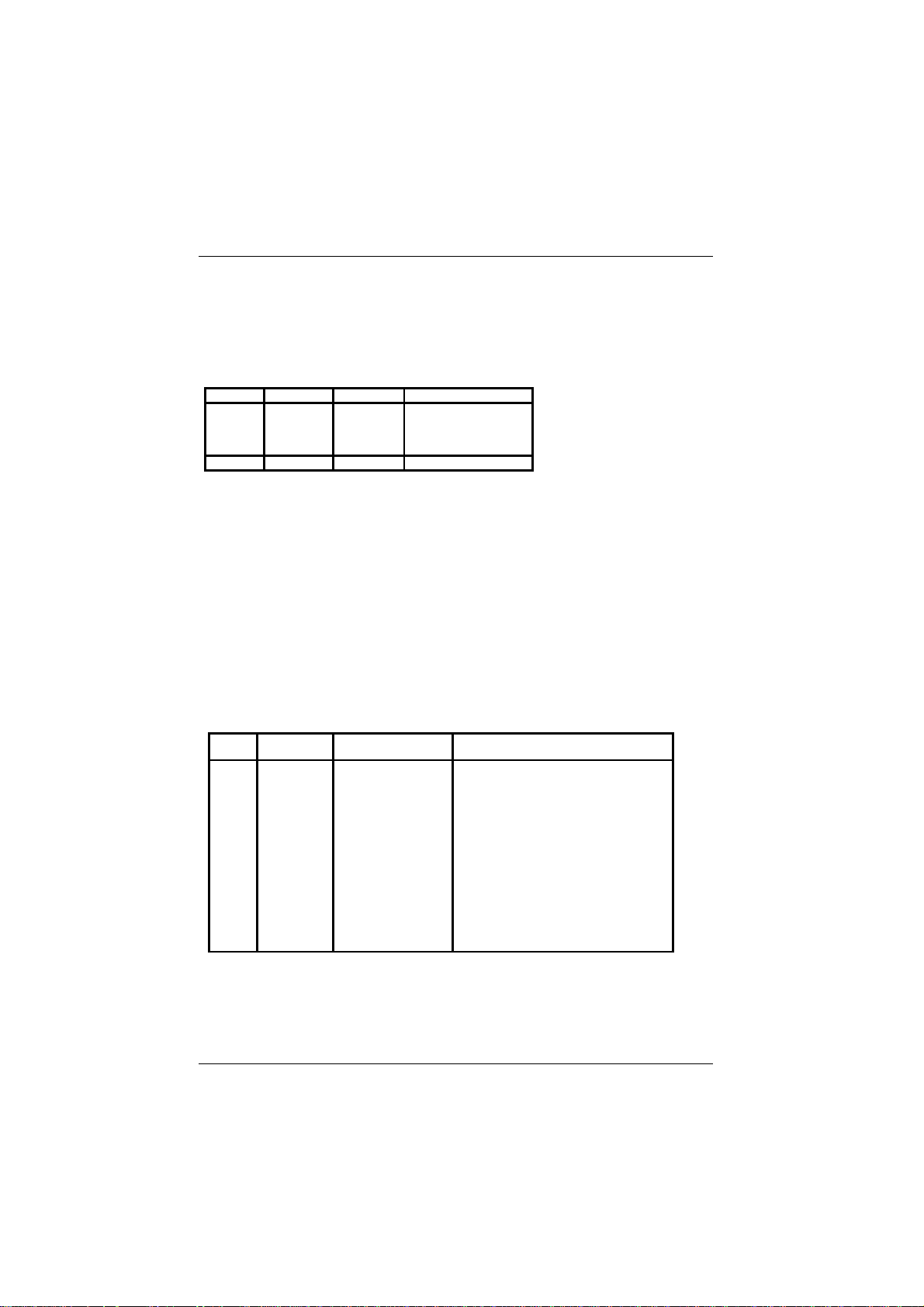
The APEX comes equipped with a serial E²PROM, 64 bytes of which are
available for user configuration in formation. Access to the device ca n be ma de
through the APEX BIOS extensions ( See APEX software utilities section).
I/O Hex Access Operator Action
0100 Write Bit 0
Bit 1
Bit 2
Bit 3
0100 Read Bit 0 Read E²PROM data
E²PROM Chip Select
E²PROM Clock Signal
E²PROM Write Data
Flash Access
The Flash device has a capacity of either 128KB, 256KB, 512KB or 1MB (Rev
C only). The Flash device is located in memory at E0000H to EFFFFH (64KB).
To access all of the Flash device it is necessary to page 64KB sections into the
window at E0000H. This is achieved by writing a data byte to 102H thereby
accessing the Flash as shown below. It is important to insure that the code being
executed is not in Flash when pages are switched. If this were to happen CPU
control would be lost. The on-board generated 12 volts will be applied to the
Flash when bit 3 is set high (providing J1 is fitted). To program the Flash device
the supplied Blue Chip Technology utility "ProgFlash" should be used.
I/O
Hex
0102 Read/Write
Access Operator Action
Selects a 64KB page in the Flash device.
Selects 00000-0FFFFH in Flash
Selects 10000-1FFFFH in Flash
Selects 20000-2FFFFH in Flash
Selects 30000-3FFFFH in Flash
Selects 40000-4FFFFH in Flash
Selects 50000-5FFFFH in Flash
Selects 60000-6FFFFH in Flash
Selects 70000-7FFFFH in Flash
Selects 80000-1FFFF in Flash
0 - Disable Flash Programming Voltage
1 - Enable Flash Programming Voltage
1 - Set user output
0 - Reset user output
Read/Write
Write
Data Bits 0-2,5
0000 (128 - 128KB)
0001 (128 - 512KB)
0010 (256 - 512KB)
0011 (256 - 512KB)
0100 (512KB - 1MB)
0101 (512KB - 1MB)
0110 (512KB - 1MB)
0111 (512KB - 1MB)
1111 (1MB only)
Data Bit 3
Data Bit 4
Blue Chip Technology 127-150
Page 47

APE X 104
Page
39
Note : J3 is used to select the 512 KB devices only and must be fitted to position
1 in order to access these devices.
The user out put on bit 4 can be u sed t o di r ectl y dr ive a n LED con n ect ed bet ween
pins 13 and 14 on connector P4
On-board Serial and Parallel Ports
The APEX processor card has a 16C452 peripheral device fitted as standard.
This offers two serial and one parallel ports. These ports can be disabled via
software control.
Serial Ports
The 16C452 provides two compatible asynchronous serial ports. These are
mapped as follows:
Serial Port I/O Address Interrupt Interface Connector
1 03F8 Hex (COM1) 4 RS232 P8
2 02F8 Hex (COM2) 3 RS485 P9
This configuration cannot be changed other than to disable it.
Parallel Port
The APEX provides one fully compatible uni-directional parallel printer port. It
has a fixed configuration as detailed below and can be enabled or disabled using
the setup utility.
Parallel Port I/O Address Interrupt Connector
1 0378 Hex (LPT1) 7 P6
Blue Chip Technology 127-150
Page 48

APE X 104
Page
40
Battery
The APEX requires an external battery to be fitted to connector P5. This should
have an output of 3.6 volts, capacity of 1.8AH and be fitted with a 10K series
resistor for safety. This battery provides power for the Real Time Clock and
CMOS RAM when there is no power applied to the board. Under normal
conditions the recommended battery should last for several years.
Great care should be taken with this battery;
under NO circumstances should
:
the outputs be shorted
be exposed to temperatures in excess of 100°C
be burned
be immersed in water
be unsoldered
be recharged
be disassembled
If the battery is mistreated in any way there will be a possibility of fire,
explosion. and harm.
For battery connector pinouts see page 46.
Backplane
APEX combines the FULL driving capability of the traditional IBM/AT and the
compact physical arrangement of the PC/104 specification. The pinouts are
detailed in depth in the connector section.
The PC/104 interface as provided by APEX allows for cards to be stacked on top
of one another or optionally to be interfaced to a traditional IBM/AT backplane.
This interfacing is achieved by using the APX-PC adaptor card. This
configuartion is particularly valuable when in the early stages of a development
allowing the APEX processor to directly control current PC/AT cards or
prototypes.
The APEX is capable of driving up to an 8 slot multilayer backplane with the
appropriate termination.
Blue Chip Technology 127-150
Page 49

APE X 104
Page
41
Backplanes are available with three possible types of termination:
None Not recommended for backplanes with more than 2/3 slots
Resistive Recommended for small backplanes (<6 slots)
RC Essential for 8 slot backplanes.
The actual val ues of termination depend upon the particular installation. Please
contact your supplier for assistance.
Blue Chip Technology 127-150
Page 50

APE X 104
Memory Map
Typical Memory Map for a 1MByte APEX CPU & CI 2
1MB 100000
BIOS/Shadow BIOS
Flash 64KB Page
Available For Expansion
adapters
APEX BIOS
Extensions
Video BIOS/Shadow BIOS
Video
Memory
Array
640KB
FFFFF
F0000
EFFFF
E0000
DFFFF
D0000
C8000
C0000
BFFFF
A0000
9FFFF
Page
42
Base Memory
Blue Chip Technology 127-150
Page 51

APE X 104
Page
43
APEX Configuration Jumpers
Jumper Area of Influence Link Action
J1 APEX generated +12 Volts
applied to FLASH
J2 On-board Video BIOS None
J3 On-board FLASH selection Factory
J4 Select DRAM size 2M
J5 On-board Serial port RS485 mode 1
J6 On-board Serial port RS485 mode Fitted
None
Fitted
Fitted
Fitted
8M
2
None
Not applied - programming
disabled
Applied - programming
enabled
Enabled
Disabled
Position 1 for 512KB only
512KByte or 2MB fitted
8MB fitted
Half Duplex selected
Full Duplex selected
Half Duplex selected
Full Duplex selected
Note
When half duplex RS485 mode is selected, DTR is used to direction control.
With DTR asserted in the half duplex mode the RS485 transceiver is
transmitting.
Blue Chip Technology 127-150
Page 52

APE X 104
APEX Connector Pinouts
P1: PC/104 8 bit (64 way)
A Signal B Signal
1 -IOCHCK 1 0 Volts (Ground)
2 SD7 2 Resetdrv
3 SD6 3 +5 Volts
4 SD5 4 IRQ9
5 SD4 5 -5 Volts
6 SD3 6 DREQ2
7 SD2 7 -12 Volts
8 SD1 8 -0WS
9 SD0 9 +12 Volts
10 IOCHRDY 10 0 Volts (Ground)
11 AEN 11 -SMEMW
12 SA19 12 -SMEMR
13 SA18 13 -IOW
14 SA17 14 -IOR
15 SA16 15 -DACK3
16 SA15 16 DREQ3
17 SA14 17 -DACK1
18 SA13 18 DREQ1
19 SA12 19 -REF
20 SA11 20 CLK
21 SA10 21 IRQ7
22 SA9 22 IRQ6
23 SA8 23 IRQ5
24 SA7 24 IRQ4
25 SA6 25 IRQ3
26 SA5 26 -DACK2
27 SA4 27 T/C
28 SA3 28 BALE
29 SA2 29 +5 Volts
30 SA1 30 OSC
31 SA0 31 0 Volts (Ground)
32 0 Volts Ground) 32 0 Volts (Ground)
Page
44
Blue Chip Technology 127-150
Page 53

APE X 104
P2: PC/104 16 bit (40 way)
D Signal C Signal
1 0 Volts (Ground) 1 0 Volts (Ground)
2 -SBHE 2 -MEMCS16
3 LA23 3 -IOCS16
4 LA22 4 IRQ10
5 LA21 5 IRQ11
6 LA20 6 IRQ12
7 LA19 7 IRQ15
8 LA18 8 IRQ14
9 LA17 9 -DACK0
10 -MEMR 10 DREQ0
11 -MEMW 11 -DACK5
12 SD8 12 DREQ5
13 SD9 13 -DACK6
14 SD10 14 DREQ6
15 SD11 15 -DACK7
16 SD12 16 DREQ7
17 SD13 17 +5 Volts
18 SD14 18 -Master
19 SD15 19 0 Volts (Ground)
20 No Connection 20 0 Volts (Ground)
Page
45
P3: 3½" Disk Drive (4 way header)
Pin No. Signal
1 +5 Volts DC
2 0 Volts (Ground)
3 0 Volts (Ground)
4 +12 Volts DC
Blue Chip Technology 127-150
Page 54

APE X 104
P4: Peripheral (20 way header)
Pin No. Signal Pin No. Signal
1 Audio +ve 2 Audio -ve
3 Reset +ve 4 Reset -ve (Ground)
5 Turbo LED +ve 6 Turbo LED -ve
7 Keyboard inhibit 8 0 V (Ground)
9 Power LED +ve 10 Power LED -ve (Ground)
11 Mouse Data 12 Mouse clock
13 220WPull up 14 Reserved
15 +5V (fused) 16 0 Volts (Ground)
17 +ve Battery input 18 0 Volts Battery (Ground)
19 Keyboard Data 20 Keyboard Clock
P5: Battery (3 way header)
Pin No. Signal
1 +3.6 Volts DC
2 Not used (key)
3 0 Volts (Ground)
4 0 Volts (Ground)
Page
46
Blue Chip Technology 127-150
Page 55

APE X 104
P6: Parallel (26 way header)
Pin No. Signal Pin No. Signal
1 -Strobe 2 -Auto Feed XT
3 Data bit 0 4 -Error
5 Data bit 1 6 -Initialise
7 Data bit 2 8 -Select (input)
9 Data bit 3 10 0 Volts (Ground)
11 Data bit 4 12 0 Volts (Ground)
13 Data bit 5 14 0 Volts (Ground)
15 Data bit 6 16 0 Volts (Ground)
17 Data bit 7 18 0 Volts (Ground)
19 -Acknowledge 20 0 Volts (Ground)
21 Busy 22 0 Volts (Ground)
23 Paper Empty 24 0 Volts (Ground)
25 Select (Output) 26 Not Used
P7: Co-Processor (36 way header)
Pin No. Signal Pin No. Signal
1 +5 Volts 2 LD14
3 +5 Volts 4 LD15
5 +5 Volts 6 -READY
7 +5 Volts 8 -M/IO
9 LD0 10 PROCLK
11 LD1 12 RESET
13 LD2 14 -BUSY
15 LD3 16 -ADS
17 LD4 18 -W/R
19 LD5 20 -NPBUSY
21 LD6 22 -NPERR
23 LD7 24 LA23
25 LD8 26 LA2
27 LD9 28 386PEREQ
29 LD10 30 0 Volts (Ground)
31 LD11 32 0 Volts (Ground)
33 LD12 34 0 Volts (Ground)
35 LD13 36 0 Volts (Ground)
Page
47
Blue Chip Technology 127-150
Page 56
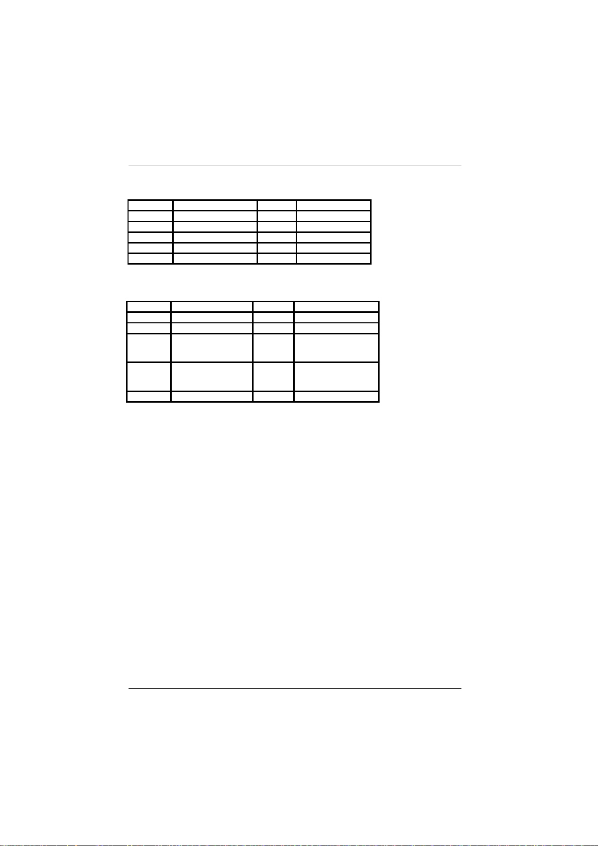
APE X 104
P8: Serial 1 RS232 (10 way header)
Pin No. Signal Pin No. Signal
1 -Data Carrier Detect 2 -Data Set Ready
3 Receive Data 4 -Ready To Send
5 Transmit Data 6 -Clear To Send
7 -Data Terminal Ready 8 -Ringing Indicator
9 0 Volts (Ground) 10 Not used
P9: Serial 2 RS485 (10 way header)
Pin No. Signal Pin No. Signal
1 Full Duplex RX +ve 2 4K7WPull up (+5V)
3 Full Duplex RX -ve 4 RESERVED
5 TX +ve Full Duplex
TX/RX +ve Half
Duplex
7 TX -ve Full Duplex
TX/RX -ve Half
Duplex
9 4K7WPull down(0V) 10 NC
6NC
8NC
Page
48
Blue Chip Technology 127-150
Page 57

APE X 104
Page
49
APEX Bus Signal Descriptions
The following is a description of the APEX (ISA) Bus signals. All signal lines
are TTL compatible.
AEN (O)
'Address Enable' is used to degate the microprocessor and other devices from the
I/O channel to allow DMA transfers t o take place. Wh en th is lin e is active, th e
DMA controller has control of the address bus, the data-bus Read command
lines (memory and I/O), and the Write command lines (memory and I/O).
BALE (O) (Buffered)
'Address latch enable' is provided by the bus controller and is used on the system
board to latch valid addresses and memory decodes from the microprocessor. It
is available to the I/0 channel as an indicator of a valid microprocessor or DMA
address (wh en used with 'AEN' ). Microprocessor addr esses SA0 thr ough SAl9
are latched with the falling edge of 'BALE. ' 'BALE' is forced high during DMA
cycles.
CLK (O)
This is the system clock. The clock has a 50% duty cycle. This signal should
only be used for synchronization. It is not intended for uses requiring a fixed
frequency.
-DACKO through -DACK3 and -DACK5 through -DACK7 (O)
-DMA Acknowledge 0 through 3 and 5 through 7 are used to acknowledge
DMA requests (DRQ0 through DRQ7). They are active low.
DRQ0 through DRQ3 and DRQ5 through DRQ7 (I)
DMA Requests 0 thr ough 3 and 5 thr ough 7 ar e asynch ronous chan nel req uests
used by peripheral devices and the I/O channel microprocessors to gain DMA
service (or control of the system). They are prioritized, with DRQ0 having th e
highest priority and DRQ7 having the lowest. A request is generated by bringing
a DRQ line to an active level. A DRQ line must be held high until the
corresponding 'DMA Request Acknowledge'(DACK) line goes active. DRQ0
Blue Chip Technology 127-150
Page 58

APE X 104
Page
50
through DRQ3 will perform 8 -bit DMA transfers; 'DRQ5' thr ough DRQ7 will
perform l6 bit transfers.
-I/O CHCK (I)
'-I/O channel check' provides the system board with parity (error) information
about memory or devices on the I/O channel. When this signal is active, it
indicates an uncorrectable system error.
I/O CHRDY (I)
'I/O channel ready' is pulled low (not ready) by a memory or I/O device to
lengthen I/O or memory cycles. Any slow device using this line should drive it
low immediately upon detecting its valid address and a Read or Write command.
Mach ine cycles are ex tend ed by an in tegr al n umber of cl ock cycles. Th is sig nal
should be held low for no more than 2.5 microseconds.
-I/O CS16 (I)
'-I/O 16 bit Chip Select' signals the system board that the present data transfer is
a 16 bit, 1 wait state, I/O cycle. It is derived from an address decode. '- I/O CS
16' is active low and should be driven with an open collector or tri-state driver
capable of sinking 20mA.
-IOR (I/O)
'-I/O Read' instructs an I/O device to drive its data onto the data bus. It may be
driven by the system mi croprocessor or DMA con troll er, or by a microprocessor
or DMA controller resident on the I/O channel. This signal is active low.
-IOW (I/O)
'I/O Write' instructs an I/O device to read the data on the data bus. It may be
driven by any micr oprocessor or DMA cont roller in the system. This sig nal is
active low.
Blue Chip Technology 127-150
Page 59

APE X 104
Page
51
IRQ3 to IRQ7, IRQ9 to IRQ12 and IRQ14 to 15 (I)
Interrupt Requests 3 through 7, 9 through 12, and 14 through 15 are used to
signal the microprocessor that an I/0 device needs attention. The interrupt
requests are prioritized, with IRQ9 through IRQ12 and IRQ14 through IRQ15
having the highest priority (IRQ9 is the highest) and IRQ3 through IRQ7 having
the lowest priority (IRQ7 is the lowest). An interrupt request is generated when
an IRQ line is raised from low to high. The line must be held high until the
microprocessor acknowledges the interrupt request (Interrupt Service routine).
LA17 through LA23 (I/O)
These signals (unlatched) are used to address memory and I/O devices within th e
system. They give the system up to 16MB of address capability. These signals
are valid when 'BALE' is high. LA17 through LA23 are not latched during
microprocessor cycles and therefore do not stay valid for the whole cycle. Their
purpose is to generate memory decodes for 1 wait- state memory cycles. These
decodes should be latched by I/O adapters on the falling edge of 'BALE. ' These
signals also may be driven by other microprocessors or DMA controllers that
reside on the I/O channel.
-Master (I)
This signal is used with a DRQ line to gain control of the system. A processor or
DMA controller on the I/O channel may issue a DRQ to a DMA channel in
cascade mode and receive a '- DACK'. Upon receiving the '- DACK', an I/O
microprocessor may pull '- Master' low, which will allow it to control the system
address, data, and control lines (a condition known as tri-state). After '- Master'
is low, the I/O microprocessor must wait one system clock period before driving
the address and data lines, and two clock periods before issuing a Read or Write
command. If this signal is held low for more than 15 microseconds, system
memory may be lost because of a lack of refresh.
-MEMCS16 (I)
'-MEM 16 Chip Select' signals the system board if the present data transfer is a 1
wait-state, 16 bit, memory cycle. It must be derived from the decode of LA17
through LA23. '-MEM CS 16' should be driven with an open collector or tristate driver capable of sinking 20 mA.
Blue Chip Technology 127-150
Page 60

APE X 104
Page
52
OSC (O)
'Oscillator' (OSC) is a high speed clock with a 70 n anosecond period (14.31818
MHz). This signal is not synchronous with the system clock. It has a 50 % duty
cycle.
0WS (I)
The 'Zero Wait State' (0WS) signal tells the microprocessor that it can complete
the present bus cycle without inserting any additional wait cycles. In order to run
a memory cycle to a 16 bit device without wait cycles, '0WS' is derived from an
address decode gated with a Read or Write command.
In order to run a memory cycle to an 8 bit device with a minimum of two wait
states, '0WS' should be driven active on system clock after the Read or Write
command is active gated with the address decode for the device. Memory Read
and Write commands to a 8 bit device are active on the falling edge of the
system clock. '0WS' is active low and should be driven with an open collector or
tri-state driver capable of sinking 20 mA.
-Refresh (I/O)
This signal is used to indicate a refresh cycle and can be driven by a
microprocessor on the I/O channel.
Reset Drive (O)
'Reset drive' is used to reset or initialize system logic at power up time or when
the power supply drops below its minimum level. This signal is active high.
SA0 through SAl9 (I/O)
Address bits 0 through 19 are used to address memory and I/O devices within
the system. These twenty address lines, in addition to LA17 through LA23,
allow access of up to 16MB of memory. SA0 through SAl9 are gated on the
system bus when 'BALE' is high and are latched on the falling edge of 'BALE. '
Blue Chip Technology 127-150
Page 61

APE X 104
Page
53
These signals are generated by the microprocessor or DMA Controller. They
also may be driven by other m icroprocessors or DMA cont rollers t hat r eside on
the I/O channel.
Blue Chip Technology 127-150
Page 62

APE X 104
Page
54
SBHE (I/O)
'Bus High Enable' (system) indicates a transfer of data on the upper byte of the
data bus, SD8 through SD15. 16 bit devices use 'SBHE' to condition data bus
buffers tied to SD8 through SD15.
SD0 through SD15 (I/O)
These signals provide data bus bits 0 through 15 for the microprocessor,
memory, and I/O devices. D0 is the least significant bit and Dl5 is the most
significant bit. All 8 bit devices on the I/O channel should use D0 through D7
for communications to the microprocessor. The l6 bit devices will use D0
through D15. To support 8 bit devices, the data on D8 through D15 will be gated
to D0 through D7 during 8 bit transfers to these devices. 16 bit microprocessor
transfers to 8 bit devices will be converted to two 8 bit transfers.
-SMEMR (O)- MEMR (I/O)
These signals instruct the memory devices to drive data onto the data bus. 'SMEMR' is active only when the memory decode is within the low lMB of
memory space. '- MEMR' is active on all memory read cycles. '- MEMR' may be
driven by any micropr ocessor or DMA contr oller in th e system. '- SMEMR' is
derived from 'MEMR' and the decode of the low lMB of memory. When a
microprocessor on the I/O channel wishes to drive '- MEMR', it must have the
address lines valid on the bus for one system clock period before driving 'MEMR' active. Both signals are active low.
-SMEMW (O)- MEMW (I/O)
These signals instruct the memory devices to store the data present on the data
bus. '- SMEMW' is active only when the memory decode is within the low 1 MB
of the memory space. '- MEMW' is active on all memory write cycles. '- MEMW'
may be driven by any microprocessor or DMA controller in the system. 'SMEMW' is derived from '- MEMW' and the decode of the low lMB of memory.
When a microprocessor on the I/O channel wishes to drive '- MEMW', it must
have the address lines valid on the bus for one system clock period before
driving '- MEMW' active. Both signals are active low.
T/C (O)
Blue Chip Technology 127-150
Page 63

APE X 104
Page
55
'Terminal Count' provides a pulse when the terminal count (end of) for any
DMA channel is reached.
Blue Chip Technology 127-150
Page 64
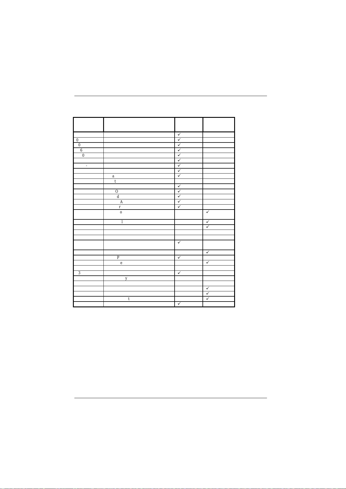
APE X 104
I/O Address Map
Page
56
Hex Range Device Occupied by
0000 - 00lF DMA Controller 1
0020 - 003F Interrupt Controller 1, Master
0040 - 005F Timer & Index registers for SCATsx
0060 - 006F 8042 (Keyboard & Mouse)
0070 - 007F Realtime Clock, NMI Mask
0080 - 008F POST, DMA Page Register
00A0 - 00BF Interrupt Controller 2, Slave
00C0 - 00DF DMA Controller 2
00F0 Clear Maths Coprocessor Busy
00F1 Reset Maths Coprocessor
00F8 - 00FF Maths Coprocessor
0100H E²PROM Access
0101H Watchdog
0102H FLASH Access
0103H Peripheral disable
0104H Serial Port Rs232 or 485/ Half or Full
Duplex
0105H 24 Digital I/O
01F0 - 01F8 Hard (fixed) Disk Controller
0200 - 0207 Games port
0278 - 027F Parallel Printer Port 2
0208 - 021A E MS Page registe rs ( e ithe r 208 or 218,
etc)
02E8 - 02EF Serial Port 4
02F8 - 02FF Serial Port 2
0300 - 031F Prototype Card/Digital PIO
0360 - 036F Reserved
0378 - 037F Parallel Printer Port 1
0380 - 038F SDLC, Bi-synchronous 2
03A0 - 03AF Bi-synchronous 1
03B0 - 03DF Video Adapter
03E8 - 03EF Serial Port 3
03F0 - 03F7 Floppy Diskette Controller
03F8 - 03FF Serial Port 1
APEX
(default)
9
9
9
9
9
9
9
9
9
9
9
9
9
9
9
9
9
9
Occupied by
APEX-CI 2
(default)
9
9
9
9
9
9
9
9
Blue Chip Technology 127-150
Page 65
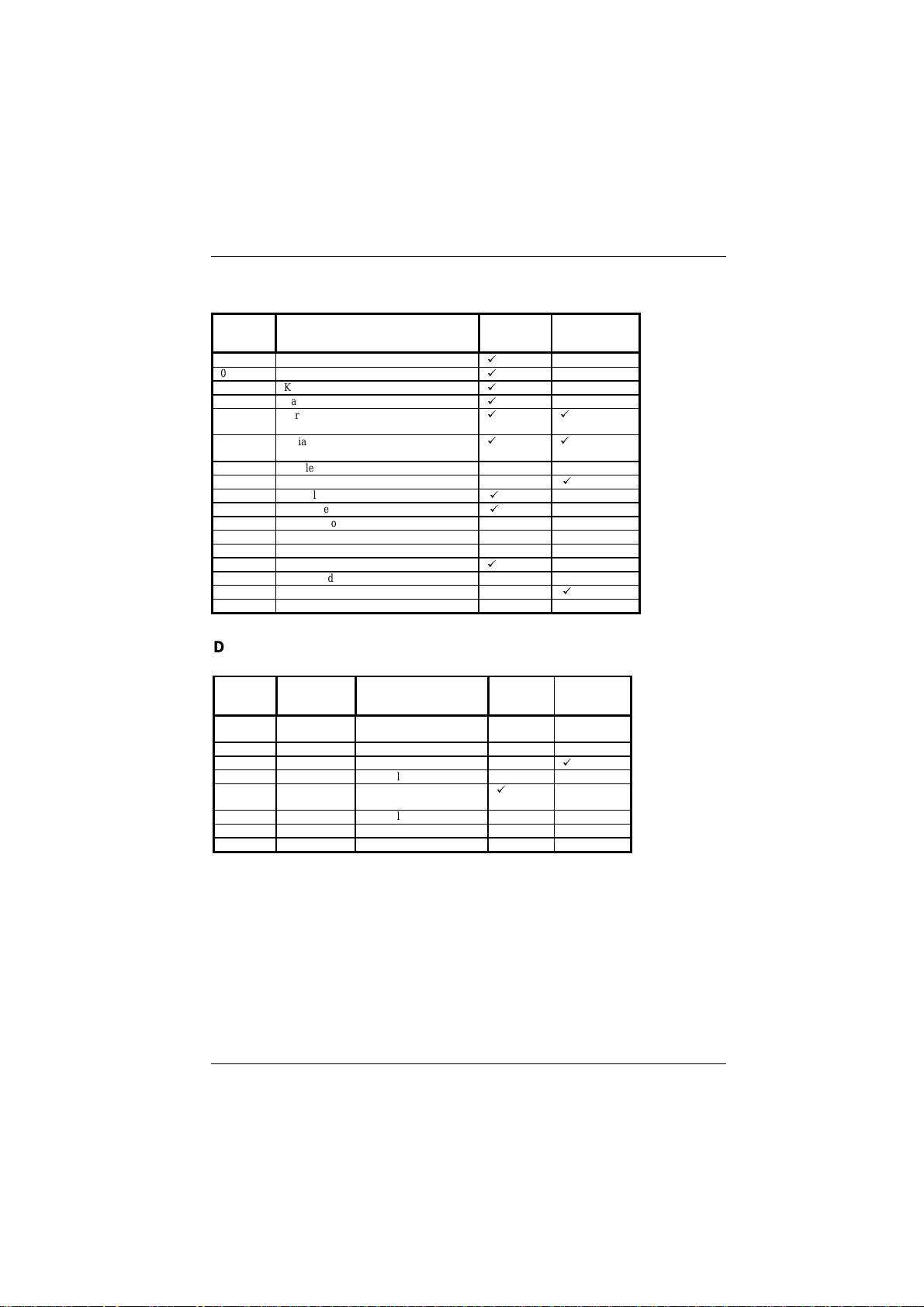
APE X 104
Interrupt Assignments
Page
57
Interrupt Device Occupied
NMI Parity Check (generates IOCHCK on error)
0 Timer
1 Keyboard (Output Buffer Full)
2 Cascaded from Interrupt 9
3 Serial Port 2 (also 4, 6 & 8 if sharing
interrupts)
4 Serial Port 1 (also 3, 5 & 7 if sharing
interrupts)
5 Parallel Port 2
6 Floppy Diskette Controller
7 Parallel Port 1
8 Real Time Clock
9 VGA controller
10 Unassigned
11 Unassigned
12 PS/2 Mouse
13 Unassigned
14 Hard (Fixed) Disk Controller
15 Unassigned
on APEX
(default)
9
9
9
9
99
99
9
9
9
DMA Assignments
DMA
Channel
0 8 bit Available (usually Refresh
1 8 bit Available
2 8 bit Diskette Drive
3 8 bit Available
4 16 bit Cascaded to 1st DMA
5 16 bit Available
6 16 bit Available
7 16 bit Available
8/16 bit
Peripherals
Device Occupied
but free on APEX)
controller
on APEX
(default)
9
Occupied by
APEX-CI 2
(default)
9
9
Occupied by
APEX-CI 2
(default)
9
Blue Chip Technology 127-150
Page 66

APE X 104
Page
58
POST Error Codes
The BIOS performs a Power On Self Test a fter a r eset or r eboot. Durin g the
POST the m icroprocessor ind icates the state of the test by writing codes to the
I/O port address 80 hex. The APEX offers on-board decode of this information
and can drive the optional POST display without modification. The following
codes indicate the progress of the microprocessor during the test.
Code
(Hex)
01 Processor register test starting. NMI disabled next.
02 NMI disabled. Power-on delay starting.
03 Power-on delay complete. Keyboard initialisation.
04 Keyboard initialisation complete.
05 Checking soft or cold start via keyboard SYS bit.
06 Enabled ROM. Calculating BIOS checksum.
07 Sending BAT command to the keyboard controller.
08 BAT command sent.
09 BAT verified.
0A Keyboard command code byte sent.
0B Keyboard command data byte sent.
0C Keyboard controller blocked and unblocked.
0D Keyboard controller NOP command complete.
0E CMOS RAM shutdown register test passed.
0F CMOS RAM checksum complete and the DIAG byte is written.
10 CMOS RAM initialised.
11 CMOS RAM status register initialised.
12 DMA and Interrupt controllers disabled.
13 Video display disabled.
14 SCATsx initialisation complete. Auto memory detection complete.
15 8254 timer channel 2 test half complete.
16 8254 timer channel 2 test complete.
17 8254 timer channel 1 test complete.
18 8254 timer channel 0 test complete.
19 Memory refresh started.
1A Memory refresh toggling test completed.
1B Memory refresh test at 15uS completed.
20 Start 64KB base memory test.
21 Memory address line test completed.
22 Memory parity toggling completed.
23 Base 64KB memory read/write test passed.
24 System configuration before vector initialisation completed.
25 Interrupt vector initialisation completed.
26 8042 input port read. Turbo initialisation completed.
27 Global data initialisation done.
28 Initialisation complete.
29 Monochrome mode is set.
2A Colour mode set.
2B Parity toggle completed.
Description
Blue Chip Technology 127-150
Page 67

APE X 104
2C Initialise for video ROM done.
2D Video ROM check complete.
2E Complete video ROM processing.
2F No EGA or VGA adapter has been found.
30 Video display read/write test completed.
31 Video display read/write or retrace test failed.
32 Alternate video display read/write test passed.
33 Video display check completed.
34 Verification of video adapter done.
35 Video display mode set.
36 BIOS ROM data area check completed.
37 Cursor setting for power-on message done.
38 Display power-on message.
39 New cursor position has been read and saved.
3A BIOS identification string displayed.
3B Hit "DEL" message displayed.
40 Prepare virtual mode test.
41 Verifying display memory completed.
42 Descriptor tables prepared.
43 Entered virtual mode.
44 Interrupts are enabled if the diagnostics switch is on.
45 Data initialised for memory wrap around check.
46 Memory wrap around check completed. Memory size check completed.
47 Memory test patterns written to extended RAM.
48 Memory test patterns written to conventional RAM.
49 Memory size below 1MB established.
4A Memory size above 1MB established.
4B BIOS ROM data area check completed.
4C Memory below 1MB cleared via a soft reset.
4D Memory above 1MB cleared via a soft reset.
4E Memory test started. No soft reset was performed.
4F Memory size display has begun. The display is updated during the test.
50 Memory test below 1MB is completed.
51 Memory size has been adjusted for memory relocation above 1MB.
52 Memory test above 1MB complete.
53 CPU registers saved.
54 CPU in real mode. Shutdown successful.
55 CPU registers restored.
56 Gate A20 address line disabled.
57 BIOS ROM data area check partially complete.
58 BIOS ROM data area check complete.
59 "Hit DEL" message has been cleared.
60 DMA page register test passed.
61 Display memory test completed.
62 DMA controller1 test passed.
63 DMA controller2 test passed.
64 BIOS ROM data area check partially complete.
65 BIOS ROM data area check complete.
66 DMA controllers 1&2 programmed.
67 8259 interrupt controller initialisation done.
80 Keyboard test started.
Page
59
Blue Chip Technology 127-150
Page 68

APE X 104
81 Keyboard reset command passed.
82 Keyboard controller interface test done.
83 Command byte written and global initialisation complete.
84 Lock key checking done.
85 Memory size check done.
86 Password has been checked.
87 Programming before Setup complete.
88 Returned from Setup program and cleared the screen.
89 Programming after Setup completed.
8A The power-on screen message is displayed.
8B The "Wait..." message is displayed.
8C System and video BIOS shadowing successful.
8D Setup options are programmed.
8E Mouse test and initialisation done.
8F Floppy Disk check identify that the drive needs initialising.
90 Floppy Disk configuration complete.
91 Hard Disk presence check completed.
92 Hard Disk configuration completed.
93 BIOS ROM data area check partially complete.
94 BIOS ROM data area check fully completed.
95 Memory size adjusted because of mouse support and hard disk type 47.
96 Display memory verified.
97 Pre-initialisation for expansion ROM operation completed.
98 Expansion ROM control test completed.
99 Initialisation for option ROM test completed.
9A Set timer data area and parallel printer base address.
9B Set asynchronous base addresses.
9C Initialisation for coprocessor test completed.
9D Coprocessor partially initialised.
9E Coprocessor initialised.
9F Extended keyboard flags checked.
A0 Keyboard ID command issued.
A1 Keyboard ID flag reset has been done.
A2 Cache memory test completed.
A3 Soft error test completed.
A4 Keyboard typematic rate is set.
A5 Memory wait states set.
A6 Screen cleared.
A7 NMI and parity enabled.
A8 Initialisation before E0000H adapter ROM control invoked.
A9 E0000H adapter ROM control completed.
00 System configuration displayed. Passing control to INT 19H boot strap
Loader now.
Page
60
Blue Chip Technology 127-150
Page 69
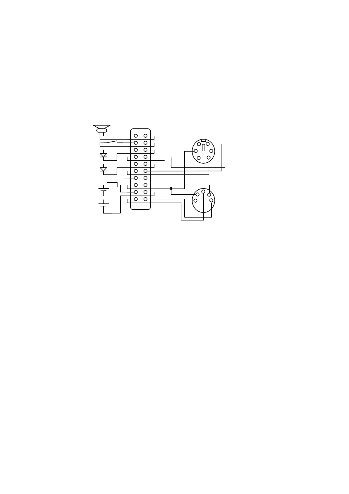
APE X 104
Wiring to the Peripheral Connector
Page
61
Speaker
-Ve +ve
Reset
Switch
Turbo
Led
Power
Led
Option 1
Battery
3.6v
P4
1
N/C
+
10k
-
2
N/C
Rear View
Keyboard
5 Pin DIN
Socket
PS/2 Mouse
Front View
6 Pin Mini Din
6
5
34
12
Please note that all LED drive outputs have a 220 ohm serial r esistor connected
to the +5 volt supply rail, and the +5v supply to the keyboard is fused (via a
SMD fuse) at 1 Amp.
Blue Chip Technology 127-150
Page 70

APE X 104
Page
62
Apex BIOS Extensions
The APEX provides a BIOS extension at address C800:0000 which pr ovides the
programmer with access to the additional hardware found on the board. The
BIOS extension hooks into software interrupt 50. The programmer loads a
particular function code into the AH register followed by a specific set of
parameters in the other registers before executing the interrupt. Most high level
languages allow access to software interrupts through a particular function call.
For example, in Quick Basic :-
' Read E2 Data via interrupt 50 call
$include:'QB.BI'
DIM INARY%(7),OUTARY%(7)
CONST AX=0,BX=1,CX=2,DX=3,BP=4,SI=5,DI=6,FL=7
INARY%(AX) = &H0400 ' Read e2 data
INARY%(BX) = &h21 ' address &h31
CALL INT86OLD(&h50,INARY%(),OUTARY%()) ' Call the APEX ' service
PRINT "E2 ADDRESS &h31 CONTAINS: ";OUTARY%(DX)
Similarly in C :-
#include <stdio.h>
#include <dos.h>
#define APEX 0x50
void main(void)
{
union REGS regs;
regs.x.ax = 0x0400; /* read e2 */
regs.x.bx = 0x31; /* address 0x31 */
int86(APEX, ®s, ®s);
printf("e2 Address 0x31 contains %x\n",regs.x.dx);
}
Blue Chip Technology 127-150
Page 71

APE X 104
Page
63
Flash Memory Functions
The APEX has on-board Flash memory options of 128KB, 256KB, 512KB and
1MB. Flash memory is similar to UV erasable EPROM in that all the memory
locations must be erased before it can be reprogrammed. The advantage over
EPROM is that Flash can be erased electrically with the device in situ.
The APEX BIOS Extension provides 3 functions which allow the programmer
access to
the flash memory, these are:
A. Read one or more FLASH Sectors into RAM
B. Write one or more FLASH Sectors
C. Erase all FLASH
Read FLASH Sector
Calling Registers: AH = 00
AL = Device number (00 for internal flash)
CX = Number of sectors to transfer
DX = Start Sector
DS:BX = Pointer to users buffer
Return Registers:
Carry Clear if successful
Carry Set if unsuccessful with error code in AX
This function is provided to allow transfer of data from the internal FLASH
EPROM. Each FLASH sector is 512 bytes long. The maximum value for the
starting sector is 254.
Blue Chip Technology 127-150
Page 72

APE X 104
Page
64
Write FLASH Sector
Calling Registers: AH = 01
AL = Device number (00 for internal
flash)
CX = Number of sectors to transfer
DX = Start Sector
DS:BX=Pointer to users buffer
Return Registers:Carry clear if successfully
Carry set if unsuccessful
This function is provided to allow transfer of data from a user buffer to the
intern al FLASH. Each flash sector is 512 bytes long and th e maximum value for
the starting sector
is 254.
NOTE: Each flash sector can only be programmed once - in order to re-write a
sector
the FLASH FORMAT function must be called first.
FLASH Format
Calling Registers: AH = 02
Return Registers: Carry clear if successful
Carry Set if unsuccessful
This function erases the entire contents of the FLASH. Depending on the age of
the FLASH this can take up to 10 seconds to complete.
Blue Chip Technology 127-150
Page 73

APE X 104
Page
65
E2 Functions
Unlike the FLASH ROM, e2 does not require to be completely erased before a
single location is written. It is therefore more useful for storage of configuration
information.
The APEX contains 64 16bit words of e2 memory - the lower 32 are reserved for
use by Blue Chip Technology for configuration information, the top 32 are
available to the user for any purpose.
The APEX BIOS extension provides two functions to allow access to the e2
memory these are:
1. Write to a single e2 memory location
2. Read from a single e2 memory location
1. Write to e2 Memory
Calling Registers: AH = 03
BL = Location to write to (0-63)
DX = Data to Write (16 bit value)
Return Registers:
Carry flag clear if successful
Carry flag Set if unsuccessful
2. Read e2 Memory
Calling Registers: AH = 04
BL = Location to read (0-63)
Return Registers:
DX = e2 Data
Blue Chip Technology 127-150
Page 74

APE X 104
Page
66
Watchdog Facility
The APEX contains a simple hardware watchdog function. When enabled, the
watchdog will generate a hardware reset if a RESET WATCHDOG functi on cal l
is not made at least once every 1.5 seconds
Two functions are available to control the watchdog
1. Enable/Disable Watchdog function
2. Reset Watchdog
1. Enable/Disable Watchdog
Calling Registers: AH = 05
AL = 00 or 01
if AL is 00, watchdog function is disabled
if AL is 01, watchdog function is enabled
Return Registers:NONE
2. Reset Watchdog
Calling Registers: AH = 06
Return Registers:NONE
System Identification
In order to detect whether software is running on an APEX unit a function has
been provided which returns a unique unit identification.
Calling Registers: AH = 09
Return Registers: DX = 4981
Blue Chip Technology 127-150
Page 75

APE X 104
Page
67
The following C routine demonstrates the use of this function
****************************************************************
unsigned int System_ID(void)
{
// return system ID code
struct REGPACK regs;
reg.r_ax = 0x0900 // Function to return ID code
reg.r_dx = 0x0000 // Clear DX
intr(0x50,®)
// ID returned in DX
return reg.r_dx // APEX returns 0x4981
// Any other system will return 0x0
}
*****************************************************************
******
Blue Chip Technology 127-150
Page 76

APE X 104
Page
68
APEX Utilities
Remote Disk
The remote disk facility allows the APEX to communicate with floppy diskette
drives and hard disk drives through a serial communications link to a PC-based
host computer running DOS.
i. Configuration
Use the Extended Setup program to configure the remote disk - If the remote is
enabled, all other options relating to disks are overridden.
ii. Making the Connection
The remote disk requires only RX ,TX and Ground lines from the serial port to
operate correctly. Connect the RX line from the serial port on the Host computer
to the TX line on the serial port on the APEX ,and the RX line from the APEX
to the TX line on the Host
iii. The Server
In order for the host computer to operate as a server, two files are required from
the APEX UTILITIES disk, these are
REMSVR.SYS - A Device driver
SERVER.EXE - A remote disk monitor program
Copy both of th ese files onto the h ost computer, make sure that REMSVR.SYS
is copied into the root directory and add the following entry to CONFIG.SYS
DEVICE = REMSVR.SYS
If the host is using a COM port other than COM1 for communication to the
APEX add the comport number after REMSVR.SYS on this line.
Reboot the host computer and run SERVER.EXE - if the device driver is
installed correctly, the remote disk status screen will be displayed, if not, check
the entry in the CONFIG.SYS file.
Blue Chip Technology 127-150
Page 77

APE X 104
Page
69
iv. Using the Remote Disk
Connect the APEX to the Host computer an d reboot t he APEX with the Host
running the SERVER.EXE program.If all is well the APEX should display:
REMOTE DISK INSTALLED
[Connected]
Prior to booting.
The APEX will then attempt to boot fr om the h ost ' s d i sk , t h e ser ial lin k operates
at 115Kbaud - even so, the data transfer rate is typically only 2 or 3 Kbytes per
second which is slow even compared to floppy disks, so please be patient!
WARNING
The remote disk will only operate correctly with operating systems which rely on
the BIOS disk services for disk access - certain operating systems such as
WINDOWS which communicate directly with disk hardware will cause the
remote disk to hang. In extreme cases data on the disk can be corrupted - Blue
Chip Technology accept no responsibility for data corrupted in this way, we
recommend that the remote disk is used initially to access floppy drives only,
where potential damage is less likely.
Blue Chip Technology 127-150
Page 78
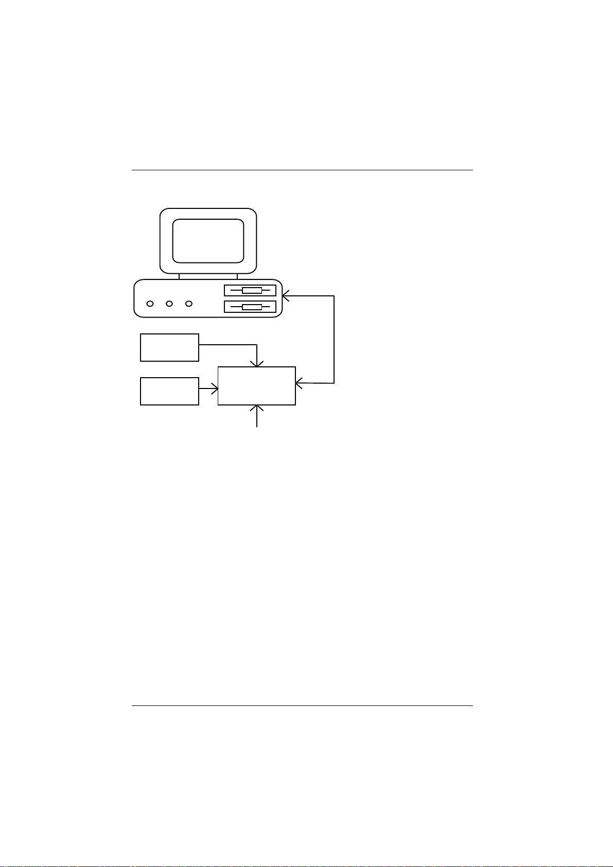
APE X 104
y
g
g
Overview
70
Page
Desk Top
I/O Res Turbo
Keyboard
Display
PC
A
C
APEX CPU
PC runs Server Pro
which lets the APEX CPU
access the PC's drive A:
Com1
Power Input
APEX unit runs special Remote Disk
pro
ram via the BIOS
ram
Simple 3 wire
RS232 Serial Link.
Link Normall
on
Com1 of the PC
to Com1 of the
APEX unit
Blue Chip Technology 127-150
Page 79

APE X 104
Page
71
Flash Disk
The on-board FLASH can be configured to appear to the system as a r ead only
720KB or 1.44MB floppy disk. Use the Extended Setup program to enable the
FLASH as either drive A or drive B.
In order to copy files onto the FLASH first take a blank
formatted diskette. Copy the files required on the FLASH disk onto this diskette.
Once all the required files are assembled on the diskette run the program
PROGFLSH.EXE, found on t he APEX UTILIT IES disk - the command line for
this p rogr am is PROGFLASH <src. drive> , where sr c. dr ive is the sour ce drive
of the floppy diskette containing the files to be copied on the FLASH Disk.
PROGFLASH will copy from the diskette onto the FLASH Disk. The FLASH
Disk is now ready for use.
For APEX systems which contain no floppy drives, a utility is provided which
copies data from a floppy disk on a remote PC.
The program PFREMOTE.EXE operates in exactly the same way as
PROGFLAS.EXE except th e disk i s copied from an other computer con nected to
the APEX via a serial cable.
To use PFREMOTE the host system must be prepared by loading the Remote
Disk Server REMSVR.SYS.
Add the line :
DEVICE = REMSVR.SYS <port>
to the CONFIG.SYS file, add ,port . to specify the serial port the host will use to
communicate with the APEX.
Now load the program SERVER.EXE on the host system.
Connect COM1 on the APEX to the host serial port (the cable should cross TX
and RX, no modem control signal need be connected).
Blue Chip Technology 127-150
Page 80

APE X 104
Page
72
The host is now ready for remote access. To re-program the FLASH disk on the
APEX run PFREMOTE.EXT on the APEX (the command line is the same as
PROGFLAS.EXE and in sert th e 720KB disk to copy into the floppy drive of the
host system.
Blue Chip Technology 127-150
Page 81

APE X 104
Page
73
APEX CI-2
Introduction
The APEX-CI 2 is a member of the APEX 104 family. It stacks to the APEX
104 CPU via the PC/104 compatible interface (P1 & P2). The APEX-CI 2
provides standard computer interfaces by the use of two VLSI devices. These
are:
CL-GD6235 which provides VGA compatible video output to both CRT & LCD
displays. SMC37C663 which provides floppy, ID & 2 serial ports
For further information on these devices please contact your supplier.
Specification
On-board Features
VGA compatible with CRT resolutions up to 1024 by 768 by 16 colours
•
with 512KByte video memory as standard
VGA compatible with LCD resolutions up to 640 by 480 driving mono,
•
colour STN, dual scan STN, TFT LCDs & EL displays
2 Asynchronous 16C550 compatible software selectable serial ports
•
providing either RS232 or RS485 interfaces
Dual IDE interface for embedded hard drives
•
Dual Floppy Disk controller (UPD72065B compatible) with on-chip Analog
•
data separator
24 Channel programmable I/O
•
Low power operation
•
PC/104 compatible
•
Blue Chip Technology 127-150
Page 82

APE X 104
Page
74
Video
The APEX-CI 2 offers a VGA compatible interface with resolutions up to 1024
by 768 by 16 colours.
The BIOS is re sident on the APEX pro cessor card at
memory address C0000 to C7FFF hex and is enabled/disable d by J2 on the
APEX CPU
. The data highway to APEX is via a 16 bit interface ensuring
optimum speed for graphics applications. Connections to a CRT monitor are
made via P7 on the APEX CI-2 . This is a 10 way header and requires a n custom
cable to in terface to t he stan dard 15 wa y conden sed D type connect or u sed on
most monitors. The CRT output is compatible with VGA mono, colour and
multisync monitors.
Connections to the LCD output are made via P4 on the APEX CI-2. This is a 40
way socket. For connection details please refer to the Display connection
Appendix at the rear of this manual.
Serial Ports
Two asynchronous 16C550 compatible interfaces are provided by the APEX-CI.
Both serial ports can operate in either RS232 or RS485 modes. When in RS485
mode either half (2 wire) or (4 wire) full duplex operation can be software
selected via the Setup menu. DTR is used for direction control. The APEX-CI 2
generates its own RS232 levels on-board allowing 5 volt only operation. The
AMI BIOS provides built-in configuration of I/O addresses and interrupt usage.
Note
If the APEX CPU’s on-board serial & parallel ports are enabled then COM1,
COM2 and LPT1 will already be occuppied. Use Extended Setup Menu to enable
and disable the APEX CPU serial ports.
Blue Chip Technology 127-150
Page 83

APE X 104
Page
75
Digital PIO
The APEX-CI 2 has an on-board 8255 (NEC 71055) I/O device allowing the up
to 24 digital (TTL) input/outputs. Connector P8 is a 26 way header providing
interfacing for three 8 bit ports and two digital grounds (0 volts). The base
address is selectable as 0200 or 0300 Hex and i s configured via th e Extended
Setup Menu.
For full details on programming this device please refer to Appendix A at the
rear of this manual.
Disk Drives
Floppy
The APEX-CI 2 has built in support for two floppy disk drives. These drives can
be any permutation of the following:
Capacity Drive Size
360KB 5¼"
720KB 3½"
1.2MB 5¼"
1.44MB 3½"
2.88MB 3½"
The BIOS Setup allows you to configure the drives for your installation.
A sta nda rd PC 34 way ri bbon cabl e with twis ted li nes ca n be con nect ed to t wo
drives both set as drive 1 (as opposed to 0). This is possible because the IBM
convention twists the drive select and motor control lines between the two drive
connections. Connection to floppy is made using P9.
Remember that only one drive in the chain should be terminated. That should be
the drive furthest from the APEX. Without correct termination drive operation
can be unreliable. In high noise environments it may be necessary to use
shielded ribbon cable. Do not extend the cable length beyond 1 metre.
Blue Chip Technology 127-150
Page 84

APE X 104
Page
76
Hard (IDE) Drive
The on-board IDE interface allows the connection of up to two hard drives.
These connect to the APEX-CI 2 via P5 which is a 40 way header. The
maximum length of ribbon cable to be used for reliable operation is 450mm.
Each drive can be one of the following 46 types or alternatively a custom type 47
(i.e. each drive can be a different type 47).
Should problems be experienced with the hard disk operation please check the
status of both J4 & J5 on the APEX-CI 2 card. J4 selects whether the ALE
(Address Latch Enable) signal is passed through to the hard drive. Where
problems are being experienced, especially in electrically noisy environments,
try changing the link.
J5 selects whether pin 34 of the IDE interface is grouded or left floating. This
should only be changed after consulting your IDE drive data sheet. With the link
present ground is applied to pin 34.
Hard Disk Types
Hard disk drive types are identified by the following parameters:
Parameter Description
Type A designation for a hard disk drive with
Cylinders The number of cylinders in the disk drive.
Heads The number of heads.
Write
Precompensation
Landing Zone The number is the cylinder location where the
Sectors The number of sectors per track. Hard drives that use MFM have
Capacity The formatted capacity of the drive based on the following
Blue Chip Technology 127-150
predefined parameters
The size of a sector gets progressively smaller
as the track diameter diminishes. Yet each sector must still hold
512 bytes. Write precompensati on circuitry difference in se ctor
size by boosting the write current for sectors on inner tracks. This
parameter is the track number where write precompensation
begins.
heads normally park when the system is shut
down.
17 sectors per track. RLL drives have 26 sectors pe r track. ARLL
and ESDI drive s have 34 s e ctors per t rack. SCSI and I D E dri ves
may have even more sectors per track.
formula:
(Number of heads) * (Number of cylinders) * (Number of
sectors per cylinder) * (512 bytes per sector)
Page 85

APE X 104
The standard 46 hard disk type are as follows:
Page
77
Type No. of
Cylinders
1 306 4 128 305 17 10MB
2 615 4 300 615 17 20MB
3 615 6 300 615 17 31MB
4 940 8 512 940 17 62MB
5 940 6 512 940 17 47MB
6 615 4 65535 615 17 20MB
7 462 8 256 511 17 31MB
8 733 5 65535 733 17 30MB
9 900 15 65535 901 17 112MB
10 820 3 65535 820 17 20MB
11 855 5 65535 855 17 35MB
12 855 7 65535 855 17 50MB
13 306 8 128 319 17 20MB
14 733 7 65535 733 17 43MB
15
16 612 4 0 663 17 20MB
17 977 5 300 977 17 41MB
18 977 7 65535 977 17 57MB
19 1024 7 512 1023 17 60MB
20 733 5 300 732 17 30MB
21 733 7 300 732 17 43MB
22 733 5 300 733 17 30MB
23 306 4 0 336 17 10MB
24 925 7 0 925 17 54MB
25 925 9 65535 925 17 69MB
26 754 7 754 754 17 44MB
27 754 11 65535 754 17 69MB
28 699 7 256 699 17 41MB
29 823 10 65535 823 17 68MB
30 918 7 918 918 17 53MB
31 1024 11 65535 1024 17 94MB
32 1024 15 65535 1024 17 128MB
No. of
heads
Write
Precompen-
sation
Landing
Zone
No. of
Sectors
Size
Blue Chip Technology 127-150
Page 86

APE X 104
33 1024 5 1024 1024 17 43MB
34 612 2 128 612 17 10MB
35 1024 9 65535 1024 17 77MB
36 1024 8 512 1024 17 68MB
37 615 8 128 615 17 41MB
38 987 3 987 987 17 25MB
39 987 7 987 987 17 57MB
40 820 6 820 820 17 41MB
41 977 5 977 977 17 41MB
42 981 5 981 981 17 41MB
43 830 7 512 830 17 48MB
44 830 10 65535 830 17 69MB
45 917 15 65535 918 17 114MB
46 1224 15 65535 1223 17 152MB
Page
78
Blue Chip Technology 127-150
Page 87

APE X 104
APEX-CI 2 Configuration Jumpers
Jumper Area of Influence Link Action
J1 Serial port 1 RS485 Duplex
termination
J2 Serial port 2 RS485 Duplex
termination
J3 LCD Mode Select 3 2 1
J4 IDE interface None
J5 IDE interface None
J6 Video Controller selection DIS
None
Fitted
None
Fitted
0 0 0
0 0 1
0 1 0
0 1 1
Fitted
Fitted
EN
No termination on-board
100R & 100nF in circuit
No termination on-board
100R & 100nF in circuit
See Table below
Panel Class 0
Panel Class 1
Panel Class 2
Panel Class 3
Removes ALE from IDE
Connects ALE to IDE
Pin 34 floats
Pin 34 is grounded
Disable
Enable
LCD Table: Note: 0 = link present, 1 = no link present
Class 0: 8 colour, single panel, single scan, 16 bit
Class 1: Monochrome, 2 shade, dual panel, dual scan, 8 bit
Class 2: 8 colour, dual panel, dual scan, 16 bit
Class 3: 256K colour,single panel, 18 bit
and 4096 colour, single panel, 12 bit
and 512 colour, single panel, 9 bit
Page
79
Blue Chip Technology 127-150
Page 88

APE X 104
APEX-CI 2 Connector Pin-outs
P1: PC/104 8 bit (64 way)
A Signal B Signal
1 -IOCHCK 1 0 Volts (Ground)
2 SD7 2 Resetdrv
3 SD6 3 +5 Volts
4 SD5 4 IRQ9
5 SD4 5 -5 Volts
6 SD3 6 DREQ2
7 SD2 7 -12 Volts
8 SD1 8 -0WS
9 SD0 9 +12 Volts
10 IOCHRDY 10 0 Volts (Ground)
11 AEN 11 -SMEMW
12 SA19 12 -SMEMR
13 SA18 13 -IOW
14 SA17 14 -IOR
15 SA16 15 -DACK3
16 SA15 16 DREQ3
17 SA14 17 -DACK1
18 SA13 18 DREQ1
19 SA12 19 -REF
20 SA11 20 CLK
21 SA10 21 IRQ7
22 SA9 22 IRQ6
23 SA8 23 IRQ5
24 SA7 24 IRQ4
25 SA6 25 IRQ3
26 SA5 26 -DACK2
27 SA4 27 T/C
28 SA3 28 BALE
29 SA2 29 +5 Volts
30 SA1 30 OSC
31 SA0 31 0 Volts (Ground)
32 0 Volts Ground) 32 0 Volts (Ground)
Page
80
Blue Chip Technology 127-150
Page 89
APE X 104
P2: PC/104 16 bit (40 way)
D Signal C Signal
1 0 Volts (Ground) 1 0 Volts (Ground)
2 -SBHE 2 -MEMCS16
3 LA23 3 -IOCS16
4 LA22 4 IRQ10
5 LA21 5 IRQ11
6 LA20 6 IRQ12
7 LA19 7 IRQ15
8 LA18 8 IRQ14
9 LA17 9 -DACK0
10 -MEMR 10 DREQ0
11 -MEMW 11 -DACK5
12 SD8 12 DREQ5
13 SD9 13 -DACK6
14 SD10 14 DREQ6
15 SD11 15 -DACK7
16 SD12 16 DREQ7
17 SD13 17 +5 Volts
18 SD14 18 -Master
19 SD15 19 0 Volts (Ground)
20 No Connection 20 0 Volts (Ground)
Page
81
P3: RS422/485 Serial (10 way header)
Pin No. Signal Pin No. Signal
1 +ve Receive Data 1 2 10KWpull up (+5V)
3 -ve Receive Data 1 4 +ve Receive Data 2
5 +ve Transmit Data 1 6 -ve Receive Data 2
7 -ve Transmit Data 1 8 +ve Transmit Data 2
9 10KWpull down (0V) 10 -ve Transmit Data 2
Blue Chip Technology 127-150
Page 90

APE X 104
P4: LCD Interface (40 way socket)
Page
82
Pin
No.
2 LCDRST 1 FPVDCLK
4 NPD 3 MOD
6 FVSYNC 5 LFS
8 FHSNYC 7 LLCLK
10 STANBY 9 R5
12 SUSPEND 11 R4
14 DE 13 R3 / SUD7
16 FPBACK 15 R2 / SUD6
18 FPVCC 17 G5 / SUD5
20 FPVEE 19 G4 / SUD4
22 VCC (APEX) 21 G3 / SUD3
24 GND (APEX) 23 B5 / SUD2
26 GND (APEX) 25 B4 / SUD1
28 GND (APEX) 27 B3 / SUD0
30 GND (APEX) 29 R1 / SLD7 / UD3
32 N/C 31 R0 / SLD6 / UD2
34 B1 / SLD1 / LD1 33 G2 / SLD5 / UD1
36 B0 / SLD0 / LD0 35 G1 / SLD4 / UD0
38 VCC (APEX) 37 G0 / SLD3 / LD3
40 N/C 39 B2 / SLD2 / LD2
Description Pin
No.
Description
Blue Chip Technology 127-150
Page 91

APE X 104
P5: IDE/Hard Drive (40 way header)
Pin No. Signal Pin No. Signal
1 -Reset 2 0 Volts DC (Ground)
3 Data bit 7 (HD) 4 Data bit 8 (HD)
5 Data bit 6 (HD) 6 Data bit 9 (HD)
7 Data bit 5 (HD) 8 Data bit 10 (HD)
9 Data bit 4 (HD) 10 Data bit 11 (HD)
11 Data bit 3 (HD) 12 Data bit 12 (HD)
13 Data bit 2 (HD) 14 Data bit 13 (HD)
15 Data bit 1 (HD) 16 Data bit 14 (HD)
17 Data bit 0 (HD) 18 Data bit 15 (HD)
19 0 Volts DC (Ground) 20 Not used
21 Not used 22 0 Volts DC (Ground)
23 -IO Write (HD) 24 0 Volts DC (Ground)
25 -IO Read (HD) 26 0 Volts DC (Ground)
27 Not used 28 ALE (HD)
29 Not used 30 0 Volts DC (Ground)
31 IRQ14 32 IOCS16
33 Address 1 (HD) 34 Ground/Float (via link)
35 Address 0 (HD) 36 Address 2 (HD)
37 -Chip Select 0 (HD) 38 -Chip Select 1 (HD)
39 IDE LED Drive 40 0 Volts DC (Ground)
Page
83
P6: Digital I/O Port (26 way header)
Pin No. Signal Pin No. Signal
1 PA0 2 PB0
3 PA1 4 PB1
5 PA2 6 PB2
7 PA3 8 PB3
9 PA4 10 PB4
11 PA5 12 PB5
13 PA6 14 PB6
15 PA7 16 PB7
17 PC0 18 PC4
19 PC1 20 PC5
21 PC2 22 PC6
23 PC3 24 PC7
25 0 Volts (Ground) 26 0 Volts (Ground)
Blue Chip Technology 127-150
Page 92
APE X 104
P7: Video (10 way header)
Pin No. Signal Pin No. Signal
1 Analogue RED 2 0 Volts (Ground)
3 Analogue GREEN 4 0 Volts (Ground)
5 Analogue BLUE 6 0 Volts (Ground)
7 Horizontal Sync 8 0 Volts (Ground)
9 Vertical Sync 10 0 Volts (Ground)
P8: Serial 1 (10 way header)
Pin No. Signal Pin No. Signal
1 -Data Carrier Detect 2 -Data Set Ready
3 Receive Data 4 -Ready To Send
5 Transmit Data 6 -Clear To Send
7 -Data Terminal Ready 8 -Ringing Indicator
9 0 Volts (Ground) 10 Not used
P9: Floppy (34 way header)
Pin No. Signal Pin No. Signal
1 0 Volts (Ground) 2 +RPM/Low Current
3 0 Volts (Ground) 4 Not used
5 0 Volts (Ground) 6 Not used
7 0 Volts (Ground) 8 -Index
9 0 Volts (Ground) 10 -Motor 0
11 0 Volts (Ground) 12 -Drive select 1
13 0 Volts (Ground) 14 -Drive select 0
15 0 Volts (Ground) 16 -Motor 1
17 0 Volts (Ground) 18 +Direction
19 0 Volts (Ground) 20 -Step
21 0 Volts (Ground) 22 -Write Data
23 0 Volts (Ground) 24 -Write Gate
25 0 Volts (Ground) 26 -Track 0
27 0 Volts (Ground) 28 -Write Protect
29 0 Volts (Ground) 30 -Read Data
31 0 Volts (Ground) 32 +Head Select
33 0 Volts (Ground) 34 +Disk Change
Page
84
Blue Chip Technology 127-150
Page 93
APE X 104
P10: Serial 2 (10 way header)
Pin No. Signal Pin No. Signal
1 -Data Carrier Detect 2 -Data Set Ready
3 Receive Data 4 -Ready To Send
5 Transmit Data 6 -Clear To Send
7 -Data Terminal
Ready
9 0 Volts (Ground) 10 Not used
8 -Ringing Indicator
P11: IDE Activity LED (2 way header)
Pin No. Signal
1 IDE LED +ve
2 IDE LED -ve
Page
85
Blue Chip Technology 127-150
Page 94
APE X 104
I/O Address Map
Page
86
Hex Range Device Occupied by
0000 - 00lF DMA Controller 1
0020 - 003F Interrupt Controller 1, Master
0040 - 005F Timer & Index registers for SCATsx
0060 - 006F 8042 (Keyboard & Mouse)
0070 - 007F Realtime Clock, NMI Mask
0080 - 008F POST, DMA Page Register
00A0 - 00BF Interrupt Controller 2, Slave
00C0 - 00DF DMA Controller 2
00F0 Clear Maths Coprocessor Busy
00F1 Reset Maths Coprocessor
00F8 - 00FF Maths Coprocessor
0100H E²PROM Access
0101H Watchdog
0102H FLASH Access
0103H Peripheral disable
0104H Serial Port Rs232 or 485/ Half or Full
Duplex
0105H 24 Digital I/O
01F0 - 01F8 Hard (fixed) Disk Controller
0200 - 0207 Games port
0278 - 027F Parallel Printer Port 2
0208 - 021A E MS Page registe rs ( e ithe r 208 or 218,
etc)
02E8 - 02EF Serial Port 4
02F8 - 02FF Serial Port 2
0300 - 031F Prototype Card/Digital PIO
0360 - 036F Reserved
0378 - 037F Parallel Printer Port 1
0380 - 038F SDLC, Bi-synchronous 2
03A0 - 03AF Bi-synchronous 1
03B0 - 03DF Video Adapter
03E8 - 03EF Serial Port 3
03F0 - 03F7 Floppy Diskette Controller
03F8 - 03FF Serial Port 1
APEX
(default)
9
9
9
9
9
9
9
9
9
9
9
9
9
9
9
9
9
9
Occupied by
APEX-CI 2
(default)
9
9
9
9
9
9
9
9
Blue Chip Technology 127-150
Page 95

APE X 104
APEX 104-CI 2 Extended I/O Port Map
Page
87
104Hex:
Serial Com port mode select register (write only)
(As per DX Rev B)
Data bit 0: primary port RS485 Full/half duplex.(0=full, 1=
half)
Data bit 1: secondary port RS485 Full/half duplex.(0=full, 1=
half)
Data bit 2: primary port RS232/485.(0=232, 1= 485)
Data bit 3: secondary port RS232/485.(0=232, 1= 485)
Note: The power on default is all bits = 0.
105Hex:
8255 enable/address select (write only)
Data bit 0: Base address select 0=200H, 1= 300H
Data bit 1: Enable/ disable 8255 0=disable, 1= enable
Note : The power on default value for each of the above is 0.
Blue Chip Technology 127-150
Page 96
APE X 104
Interrupt Assignments
Page
88
Interrupt Device Occupied
NMI Parity Check (generates IOCHCK on error)
0 Timer
1 Keyboard (Output Buffer Full)
2 Cascaded from Interrupt 9
3 Serial Port 2 (also 4, 6 & 8 if sharing
interrupts)
4 Serial Port 1 (also 3, 5 & 7 if sharing
interrupts)
5 Parallel Port 2
6 Floppy Diskette Controller
7 Parallel Port 1
8 Real Time Clock
9 VGA controller
10 Unassigned
11 Unassigned
12 PS/2 Mouse
13 Unassigned
14 Hard (Fixed) Disk Controller
15 Unassigned
on APEX
(default)
9
9
9
9
99
99
9
9
9
DMA Assignments
DMA
Channel
0 8 bit Available (usually Refresh
1 8 bit Available
2 8 bit Diskette Drive
3 8 bit Available
4 16 bit Cascaded to 1st DMA
5 16 bit Available
6 16 bit Available
7 16 bit Available
8/16 bit
Peripherals
Device Occupied
but free on APEX)
controller
on APEX
(default)
9
Occupied by
APEX-CI 2
(default)
9
9
9
Occupied by
APEX-CI 2
(default)
9
Blue Chip Technology 127-150
Page 97

APE X 104
Page
89
Appendix A - Using the Digital PIO
Introduction
The CI card contains one 8255 chip. The chip has three 8 bit ports which can be
programmed as input or output by writing a control word to the control port.
(See Table 3). Port A and B must be all input or all output. Port C may be split
into two 4 bit sections each of which may be input or output.
The chip occupies 4 read/write addresses in the IBM-PC port map.
Address
Base + 0 Port A
Base + 1 Port B
Base + 2 Port C
Base + 3 Command Port
Blue Chip Technology 127-150
Page 98
APE X 104
Output Ports
765 43210
DATA (8255 PORT A)
765 43210
DATA (8255 PORT B)
765 43210
DATA (8255 PORT C)
765 43210
Page
90
CONTROL
Control Bit Operations
Bit 0 = Port C (Lower) 0 = Output 1 = Input
Bit 1 = Port B 0 = Output 1 = Input
Bit 2 = Mode Selection 0 = Mode 0 1 = Mode 1
Bit 3 = Port C (Upper) 0 = Output 1 = Input
Bit 4 = Port A 0 = Ouput 1 = Input
Bit 5,6 = Mode Selection 00 = Mode 0
01 = Mode 1
1X = Mode 2
Bit 7 = Mode Set Flag 0 = Inactive 1 = Active
See Table 3 for Quick Set-up Guide
Blue Chip Technology 127-150
Page 99

APE X 104
Page
91
Electrical Options
Input Conditioning
The 8255 has high impedance inputs. In electrically noisy environments it is
advised to terminate the input lines with resistors. The termination may be pull
up (to 5V) or pull down to 0V).
Input/Output Connections
A 26 way insulation displacement connector (IDC) is provided (P6) on the CI
board for I/O channel signal connection. If access to individual channels is
req u ired, a 2 6 wa y IDC r i bbon cabl e m a y be us ed t o con nect t h e I / O ch a nne ls to
screw terminal blocks or other similar output connectors.
Blue Chip Technology 127-150
Page 100

APE X 104
Connector Pin Details (P6)
Pin No. Signal Pin No. Signal
1 PA0 2 PB0
3 PA1 4 PB1
5 PA2 6 PB2
7 PA3 8 PB3
9 PA4 10 PB4
11 PA5 12 PB5
13 PA6 14 PB6
15 PA7 16 PB7
17 PC0 18 PC4
19 PC1 20 PC5
21 PC2 22 PC6
23 PC3 24 PC7
25 0 Volts
(Ground)
26 0 Volts
(Ground)
Page
92
Blue Chip Technology 127-150
 Loading...