

Page 1
CUSTOMER
SUPPORT
INFORMATION
Order toll-free in the U.S. 24 hours, 7 A.M. Monday to midnight Friday: 877-877-BBOX
FREE technical support, 24 hours a day, 7 days a week: Call 724-746-5500 or fax 724-746-0746
Mail order: Black Box Corporation, 1000 Park Drive, Lawrence, PA 15055-1018
Web site: www.blackbox.com • E-mail: info@blackbox.com
AUGUST 2000
IC541A
Ultra 2 SCSI LVD/HVD
Multimode Expander
Ultra2 SCSI LVD/HVD
Multimode Expander
Page 2

1
FCC/IC STATEMENTS
FEDERAL COMMUNICATIONS COMMISSION AND INDUSTRY CANADA
RADIO-FREQUENCY INTERFERENCE STATEMENTS
Class B Digital Device. This equipment has been tested and found to comply with
the limits for a Class B computing device pursuant to Part 15 of the FCC Rules.
These limits are designed to provide reasonable protection against harmful
interference in a residential installation. However, there is no guarantee that
interference will not occur in a particular installation. This equipment generates,
uses, and can radiate radio frequency energy, and, if not installed and used in
accordance with the instructions, may cause harmful interference to radio
communications. If this equipment does cause harmful interference to radio or
telephone reception, which can be determined by turning the equipment off and
on, the user is encouraged to try to correct the interference by one of the following
measures:
• Reorient or relocate the receiving antenna.
• Increase the separation between the equipment and receiver.
• Connect the equipment into an outlet on a circuit different from that to which
the receiver is connected.
• Consult an experienced radio/TV technician for help.
Caution:
Changes or modifications not expressly approved by the party
responsible for compliance could void the user’s authority to operate
the equipment.
This digital apparatus does not exceed the Class B limits for radio noise emission from digital
apparatus set out in the Radio Interference Regulation of Industry Canada.
Le présent appareil numérique n’émet pas de bruits radioélectriques dépassant les limites
applicables aux appareils numériques de la classe B prescrites dans le Règlement sur le
brouillage radioélectrique publié par Industrie Canada.
Page 3

2
ULTRA2 SCSI LVD/HVD MULTIMODE EXPANDER
NORMAS OFICIALES MEXICANAS (NOM)
ELECTRICAL SAFETY STATEMENT
INSTRUCCIONES DE SEGURIDAD
1. Todas las instrucciones de seguridad y operación deberán ser leídas antes de
que el aparato eléctrico sea operado.
2. Las instrucciones de seguridad y operación deberán ser guardadas para
referencia futura.
3. Todas las advertencias en el aparato eléctrico y en sus instrucciones de
operación deben ser respetadas.
4. Todas las instrucciones de operación y uso deben ser seguidas.
5. El aparato eléctrico no deberá ser usado cerca del agua—por ejemplo, cerca
de la tina de baño, lavabo, sótano mojado o cerca de una alberca, etc.
6. El aparato eléctrico debe ser usado únicamente con carritos o pedestales que
sean recomendados por el fabricante.
7. El aparato eléctrico debe ser montado a la pared o al techo sólo como sea
recomendado por el fabricante.
8. Servicio—El usuario no debe intentar dar servicio al equipo eléctrico más allá
a lo descrito en las instrucciones de operación. Todo otro servicio deberá ser
referido a personal de servicio calificado.
9. El aparato eléctrico debe ser situado de tal manera que su posición no
interfiera su uso. La colocación del aparato eléctrico sobre una cama, sofá,
alfombra o superficie similar puede bloquea la ventilación, no se debe colocar
en libreros o gabinetes que impidan el flujo de aire por los orificios de
ventilación.
10. El equipo eléctrico deber ser situado fuera del alcance de fuentes de calor
como radiadores, registros de calor, estufas u otros aparatos (incluyendo
amplificadores) que producen calor.
11. El aparato eléctrico deberá ser connectado a una fuente de poder sólo del
tipo descrito en el instructivo de operación, o como se indique en el aparato.
Page 4

3
NOM STATEMENT
12. Precaución debe ser tomada de tal manera que la tierra fisica y la polarización
del equipo no sea eliminada.
13. Los cables de la fuente de poder deben ser guiados de tal manera que no
sean pisados ni pellizcados por objetos colocados sobre o contra ellos,
poniendo particular atención a los contactos y receptáculos donde salen del
aparato.
14. El equipo eléctrico debe ser limpiado únicamente de acuerdo a las
recomendaciones del fabricante.
15. En caso de existir, una antena externa deberá ser localizada lejos de las lineas
de energia.
16. El cable de corriente deberá ser desconectado del cuando el equipo no sea
usado por un largo periodo de tiempo.
17. Cuidado debe ser tomado de tal manera que objectos liquidos no sean
derramados sobre la cubierta u orificios de ventilación.
18. Servicio por personal calificado deberá ser provisto cuando:
A: El cable de poder o el contacto ha sido dañado; u
B: Objectos han caído o líquido ha sido derramado dentro del aparato; o
C: El aparato ha sido expuesto a la lluvia; o
D: El aparato parece no operar normalmente o muestra un cambio en su
desempeño; o
E: El aparato ha sido tirado o su cubierta ha sido dañada.
Page 5

4
ULTRA2 SCSI LVD/HVD MULTIMODE EXPANDER
Contents
Chapter Page
1. Specifications ............................................................................................. 5
2. Introduction ............................................................................................... 6
2.1 Overview .............................................................................................. 6
2.2 Features ............................................................................................... 8
2.3 The Complete Package ....................................................................... 8
3. Configuration and Internal LEDs ............................................................. 9
3.1 Opening the Expander ....................................................................... 9
3.2 Configuring Termination ................................................................. 11
4. Installation ................................................................................................ 14
4.1 Connecting the SCSI-Bus Cables ..................................................... 14
4.2 Connecting AC Power and Observing the External LEDs ............. 15
5. Applications .............................................................................................. 16
5.1 Applications That Will Work ............................................................ 16
5.2 Applications That Won’t Work ........................................................ 18
6. Troubleshooting ...................................................................................... 19
6.1 Calling Black Box .............................................................................. 19
6.2 Shipping and Packaging ................................................................... 19
Appendix A: Port Pinouts ............................................................................... 20
A.1 High-Voltage Differential (HVD) Pinout ........................................ 20
A.2 Low-Voltage Differential (LVD) Pinout ........................................... 20
A.3 Single-Ended (SE) Pinout ................................................................. 22
Appendix B: Block Diagram .......................................................................... 24
Page 6

5
CHAPTER 1: Specifications
1. Specifications
Compliance — FCC Part 15 Subpart J Class B, IC Class/classe B
Interfaces — LVD/SE port: Wide (16-bit) Ultra2 SCSI (“Fast 40”),
multimode (can be either LVD or single-ended,
autosensing);
HVD port: Wide (16-bit) Ultra SCSI, high-voltage
differential
Protocol — Transparent to synchronous or asynchronous
communication
Data Rate — LVD: Up to 80 Megabytes per second
Maximum
Distance — Can extend HVD SCSI bus as far as 37 m (121.3 ft.)
User Controls — (4) Internal jumpers for termination
Indicators — (2) Front-mounted LEDs: Power and Busy
Connectors — (2) Micro D68 female (see Appendix A for pinouts)
Power — 110 to 220 VAC, 50 to 60 Hz (autosensing)
Size — 2.9"H x 4.8"W x 7.8"D (7.4 x 12.2 x 19.8 cm)
Weight — 3.3 lb. (1.5 kg)
Page 7

6
ULTRA2 SCSI LVD/HVD MULTIMODE EXPANDER
2. Introduction
2.1 Overview
The Ultra2 SCSI LVD/HVD Multimode Expander is a 16-bit Wide SCSI Low
Voltage Differential (LVD) to High Voltage Differential (HVD) converter. The
Expander effectively divides the SCSI bus into one LVD or SE (single-ended)
segment (connected to its “LVD/SE” port) and an HVD segment (connected to its
“HVD” port). The Expander translates signals, and facilitates communication,
between the segments.
When used in conjunction with an Ultra2 SCSI host adapter, the Expander
maintains backward compatibility with previous generations of devices on HVD
segments, while retaining the optimal performance and maximum cable length of
LVD. The Expander can also be used with an Ultra SCSI (“SCSI-3,” 40-MB-persecond) HVD host adapter to add Ultra2 devices to its bus. Because it performs
only signal-level translation, the Expander operates transparently; users will hardly
know it’s there. It places no limits on the quantity or location of SCSI devices
beyond the normal limits of the SCSI specification.
The Expander’s LVD/SE port is “multimode,” meaning it can operate in either
single-ended or LVD mode. (This selection is controlled automatically by a sensing
signal [DIFFSENSE] provided by the SCSI devices on the bus. As soon as you
connect it to the bus, the Expander will autoconfigure its ports as necessary.)
Page 8
7
CHAPTER 2: Introduction
The Expander supports all current SCSI operations and can handle data rates up
to 20, 40, or 80 megabytes per second, depending on the type of bus it’s
communicating with. Figure 2-1 shows a typical Expander application. If you’d like
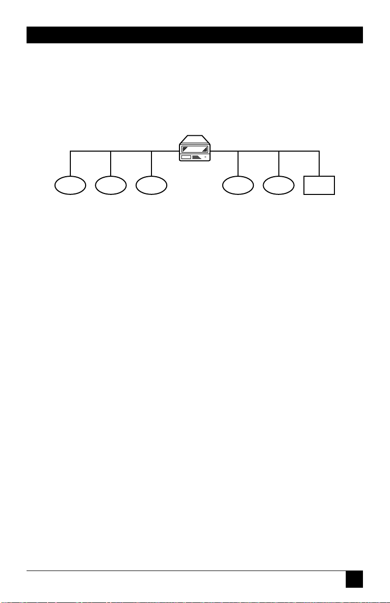
to examine a block diagram of the Expander, refer to Appendix B.
Figure 2-1. One SCSI bus with two physical segments: Using an Expander to
access legacy HVD devices with an LVD host adapter.
HVD Segment
HVD Devices
LVD Devices
Ultra2 SCSI LVD
Host Adapter
Ultra2 SCSI
LVD/HVD
Multimode
Expander
LVD Segment
Page 9

8
ULTRA2 SCSI LVD/HVD MULTIMODE EXPANDER
2.2 Features
• Supports legacy and Ultra2 SCSI devices on the same bus with LVD-to-HVD or
SE-to-HVD conversion:
– Fully backward-compatible with SCSI-1, SCSI-2 [Fast SCSI], and SCSI-3
[Ultra SCSI], and can be used with either Narrow or Wide buses.
– Has switchable internal termination.
• Transfers data at up to 80 Megabytes per second (on a 16-bit Wide bus) in
either direction.
• Supports as many as 16 SCSI devices.
• Does not require software or a SCSI ID.
• Has RS-485 HVD transceivers.
• Can be used to extend your HVD bus as far as 37 m (121.3 ft.).
• Transparent operation—requires no software and no SCSI ID.
• Supports arbitration, parity, disconnect/reconnect, and sync or async data
transfer.
• Can act as either a target or initiator on either connected SCSI-bus segment.
• LEDs show power status and bus activity at all times.
• Can optionally provide TERMPWR (terminator power) to either or both
attached bus segments. Handles TERMPWR with a resetting circuit protector
and backflow-preventing diodes.
2.3 The Complete Package
Besides the Ultra2 SCSI LVD/HVD Multimode Expander itself, you should have
received its power cord and this manual. If anything is missing or arrived damaged,
call Black Box right away.
Page 10

9
CHAPTER 3: Configuration and Internal LEDs
3. Configuration and Internal LEDs
3.1 Opening the Expander
To configure the Ultra2 SCSI LVD/HVD Multimode Expander’s termination,
you’ll need to access the Expander’s internal jumpers.
CAUTION!
To avoid receiving a potentially hazardous electric shock, make sure the
Expander is turned OFF and unplugged both when you open it and for
the entire period of time it stays open.
Conversely, even while the Expander is OFF, you need to avoid
damaging its circuit board with static electricity. If possible, stand on an
anti-static mat when you open the Extender and wear anti-static gloves
or wrist straps. At the very least, ground yourself before you open the
Expander by touching something metal.
Take these steps to open the Expander:
1. Use a small Phillips-head screwdriver to unscrew the screws embedded in each
of the Expander’s four rubber feet. Remove the feet.
2. You’ll see the edges of the Expander‘s wraparound housing on the bottom of
the unit right next to the holes where the feet used to be. If necessary, gently
pry one of these edges slightly outward so that the housing doesn’t fit so
snugly.
3. Carefully slide the housing toward the back of the unit and remove it.
Page 11

10
ULTRA2 SCSI LVD/HVD MULTIMODE EXPANDER
Now you’re ready to set the jumpers. If you look at the open Expander from above,
with its front panel facing right and its rear panel facing left, the jumper posts and
internal LEDs will be arranged at the top and bottom edges of the circuit board,
something like this:
JP4 JP1
HVD TERM ENABLE = OFF
LVD TERM ENABLE = ON
JP5
JP5 JP2
A jumper will be on the upper pair of posts at JP5 (it’s a four-position jumper); two
wires going to the external LED will be connected to JP2. All other jumper posts
will be empty. (JP4 might be hidden beneath the circuit board’s internal powercord connectors.)
Jumper posts JP1, JP4, and JP5 control termination; their possible settings are
described in Section 3.2. The JP2 jumper posts form the electrical connection to
the external Busy LED; don’t disturb this connection.
Page 12

11
CHAPTER 3: Configuration and Internal LEDs
3.1 Configuring Termination
Both ends of any SCSI-bus segment attached to the Expander need to be
terminated in order to prevent electronic “echo” interference on the bus that
would degrade its performance. You can use the Expander’s internal jumpers JP1,
JP4, and JP5 to control this termination. JP1 and the lower posts of JP5 affect the bus
attached to the HVD port , while JP4 and the upper posts of JP5 affect the bus
attached to the LVD/SE port.
• Termination at the Expander (JP5): How you should set jumpers on the four
posts at JP5, which control local termination at the Expander’s ports, depends
on how your cables will be attached to the Expander. Just remember that the
upper and lower JP5 posts have opposite values: For the lower (HVD) posts, OFF
(empty) is terminated and ON (installed) is unterminated; for the upper
(LVD/SE) posts, ON is terminated and OFF is unterminated.
– For each port into which you will be directly plugging a single cable, so that
the SCSI-bus segment will start or end at that port, leave the jumper positions
just as they come from the factory. If a segment will start or end at the HVD
port, leave the jumper OFF the lower posts. If a segment will start or end at
the LVD/SE port, leave the jumper ON the upper posts.
Example: For simple conversion applications in which an LVD bus ends at
the Expander and an HVD bus starts, or vice versa, leave the jumpers
installed on upper JP5 and leave lower JP5 empty.
– For each port into which you will be plugging two cables through a three-
connector adapter (not a stub cable!), so that the SCSI-bus segment will pass
through that port, remove the jumper. If a segment will pass through the
HVD port, install a jumper on the lower posts. If a segment will pass through
the LVD/SE port, remove the jumper from the upper posts.
Example: For applications in which you are allowing a segment of HVD
devices to tap into an LVD bus without forcing the LVD bus to operate at
the data rate of the HVD segment, remove the jumper from upper JP5. If
the HVD segment ends at the Expander, leave the lower JP5 jumper posts
empty. But if the HVD segment also passes through the Expander, install a
jumper on the lower JP5 posts.
Refer to Figures 3-1 through 3-3 on the next page. In an application such as
that shown in Figure 3-1, lower JP5 should remain empty and upper JP5 should
remain installed. In an application like that in Figure 3-2, with the Expander in
the middle of one segment and at the end of another, set the jumper oppositely
for the port that’s attached to the middle of the segment. In a wide-open
application like that in Figure 3-3, in which the Expander is in the middle of
both segments, remove the jumper from upper JP5 and install it on lower JP5.
Page 13

12
ULTRA2 SCSI LVD/HVD MULTIMODE EXPANDER
Figure 3-1. Both segments end, and are terminated, at the Expander.
Figure 3-2. One segment passes through the Expander, while the other ends
and is terminated.
Figure 3-3. Both segments pass unterminated through the Expander.
Expander
Expander
Expander
HVD bus
Lower
JP5 ON
Lower
JP5 OFF
Lower JP5 OFF
Upper JP5 ON
Upper
JP5 OFF
Upper
JP5 OFF
LVD bus
HVD bus
HVD bus
Multiconnector
ribbon cable
Multiconnector
ribbon cables
LVD bus
LVD bus
LVD
Bus
Tape drive
Disk drive
Disk drive
Host adapter
Host adapter
Host adapter
Disk drive
DVD-ROM drive
Host adapter
Termination enabled
Termination
enabled
Termination
Enabled
Termination
enabled
Termination
enabled
Disk drive
Page 14

13
CHAPTER 3: Configuration and Internal LEDs
• Termination at the Other End(s) of the Segment (JP1 and JP4): The JP1 and
JP4 jumper posts control whether or not the Expander provides TERMPWR
output to support remote termination.
To explain: Most of the current generation of SCSI host adapters, disk
drives, and other devices have built-in internal terminators, like those in the
Expander, that can be used to terminate the SCSI bus if that device happens to
be the first or last device attached to the bus. The remote ends of the SCSI-bus
segments that you’ll be attaching to the Expander will probably be able to be
terminated this way.
But if, on a SCSI segment that will be attached to the Expander, the first or
last device (or both) don’t have an internal terminator, you will need to attach
an external terminator to that device instead. That external terminator will
need to draw its power from a “terminator power” (TERMPWR) voltage that
must be present on the SCSI bus. Most SCSI devices can be set to provide
TERMPWR.
NOTE
It’s easy to make mistakes when installing external SCSI termination. If
you’ll need to do so, please call Black Box Technical Support to discuss
your application.
If the remote termination for the segments that will be attached to the
Expander can be handled with another device’s internal terminator, or with
an external terminator that gets its TERMPWR from some other device(s), you
can leave jumper posts JP1 and JP4 in their factory-default setting (no jumpers
installed). But if you’ll need to use an external terminator that gets its
TERMPWR from the Expander for remote termination on a segment attached to
either of the Expander‘s ports, install a jumper on the posts for that port.
Install a jumper on JP1 to have the Expander provide TERMPWR on its HVD
port. Install a jumper on JP4 to have the Expander provide TERMPWR on its
LVD/SE port.
Refer to Figure 3-1 on the previous page. In that illustration, the host adapter
and disk drive both have enabled internal terminators. But if the host adapter
didn’t have an internal terminator and couldn’t provide TERMPWR, you
would have to install a jumper on the Expander’s JP4 posts. If the same were
true of the disk drive, you would have to install a jumper on the Expander’s
JP1 posts.
Page 15

14
ULTRA2 SCSI LVD/HVD MULTIMODE EXPANDER
4. Installation and Operation
4.1 Connecting SCSI-Bus Cables
To attach the Ultra2 SCSI LVD/HVD Multimode Expander to one end of a SCSIbus segment, run SCSI cable from the desired port on the Expander to another
SCSI device: from the HVD port to an HVD device, from the LVD/SE port to an
LVD or SE device.
CAUTION!
Be careful not to connect HVD devices to the Expander’s LVD/SE port.
This could damage or destroy the Expander.
To tap the Expander into the middle of a segment, first turn OFF the
Expander’s internal termination for the port where you will make this
connection—see Section 3.2. Then get a (short!) “T”-style SCSI cable or adapter
with three or more connectors and plug one of its central connectors into that
port. Finally, run regular SCSI cables from the end connectors of the “T”
cable/adapter to the previous device and next device in the segment.
CAUTION!
The T adapter or cable must be wired so that it does not contain a
“stub” (does not branch)—stubbing/branching will cause your SCSI bus
to fail. Instead, the cable or adapter should be constructed so that all of
the wires run from one connector to the next, to the next, and so on, in
sequence. For LVD “T” connections, we suggest our 7-connector LVD
ribbon cable (product code EVMSCC22). For HVD or single-ended “T”
connections, we suggest our 5-connector Ultra SCSI ribbon cable
(product code EVMSCC16).
Page 16

15
CHAPTER 4: Installation and Operation
Keep in mind that the maximum cable lengths allowed on any SCSI bus are fairly
strict, though they vary by the type of bus and by the cable size and insulation. Table 4-1
lists the maximum recommended cable lengths for each type of SCSI interface that
the Expander supports.
Table 4-1. Maximum Cable Lengths
Interface Maximum Distance
HVD (any generation) 25 m (82 ft.)
SCSI-1 SE 6 m (20 ft.)
Fast/Wide (SCSI-2) SE 3 m (10 ft.)
Ultra Wide (SCSI-3) SE Fewer than 5 devices: 3 m (10 ft.);
5 or more devices: 1.5 m (5 ft.)
Ultra2 Wide LVD Multiple devices: 12 m (40 ft.);
Two devices point to point: 25 m (82 ft.)
4.2 Connecting AC Power and Observing External LEDs
Run the included power cord from the IEC 320 male inlet on the rear of the
Expander to a working AC outlet. Once you’ve plugged in the unit, flip the rocker
switch on the rear of the unit to turn the Expander ON. The green external Power
LED on its front panel should light immediately. The Expander should now be
ready for continuous operation.
The Expander’s Power LED is easy to spot, even when it’s dark; there is a special
cutout for it in the upper right-hand corner of the front panel. The amber Busy
LED isn’t so easy to see when it’s not lit; it’s embedded in the venting in the front
panel’s lower right-hand corner. However, the Busy LED will begin flashing as soon
as data begins flowing on either attached SCSI-bus segment. During exceptionally
heavy traffic conditions, the flashing might become so persistent that the LED
briefly appears to be steadily lit.
Page 17

16
ULTRA2 SCSI LVD/HVD MULTIMODE EXPANDER
5. Applications
5.1 Applications That Will Work
Here are several ways in which Ultra2 SCSI LVD/HVD Multimode Expanders can
be used in a SCSI-bus system, helping LVD and single-ended SCSI-bus segments to
work as one logical SCSI bus. (As always, each bus segment must be terminated at
both ends.)
Figure 5-1 shows how to use an Expander to allow an HVD adapter to reach LVD
devices.
Figure 5-1. Extending an HVD bus.
Expander.
lower and
upper JP5
both ON
(installed)
Multiconnector
ribbon cable
32-bit
PCI bus
HVD Bus
LVD Bus
Ultra SCSI HVD
host adapter
Termination enabled
Termination
enabled
LVD devices, max cable 12 m (40 ft.);
top data rate in this configuration 40 MB/sec
HVD devices, max
cable 25 m (82 ft.)
Page 18

17
CHAPTER 5: Applications
Figure 5-2 shows how LVD and HVD devices can be mixed with no speed
degradation for the LVD devices.
Figure 5-2. Adding legacy devices to an Ultra2 SCSI LVD bus.
Figure 5-3 shows how to use a pair of Expanders to insert maximum LVD pointto-point cable length into an HVD SCSI bus. (Normal configuration rules for HVD
segments still apply to the segments at either end of this Extender-to-Extender
link.)
Figure 5-2. Adding maximum LVD point-to-point cabling.
Expander,
lower and
upper JP5
both OFF
(empty)
Two Expanders with all ports terminated
and an LVD SCSI cable between them up
to 25 m (82 ft.) long
Multiconnector
ribbon cable
25 m (82 ft.) max
25 m (82 ft.) max
32-Bit
PCI Bus
LVD bus
HVD bus
HVD
HVD
LVD
Ultra2 SCSI
Host Adapter
Termination enabled
Termination enabled
Legacy HVD devices
Legacy HVD devices
Legacy HVD devices
Ultra2 SCSI
LVD devices
running at
top speed
Page 19

18
ULTRA2 SCSI LVD/HVD MULTIMODE EXPANDER
5.2 Applications That Won’t Work
Here are two ways that you must avoid trying to use the Expanders.
Applications like that shown in Figure 5-4 won’t work, because devices on the left
must send data through more than two Expanders to reach the devices on the
right. Two is the maximum number of Expanders through which SCSI data can
pass.
Figure 5-4. An application with too many Expanders.
Applications like that shown in Figure 5-5 won’t work either, because you can’t
have two LVD segments connected by an HVD segment. The two LVD devices
would attempt to communicate at 40 MHz, a transfer rate not supported by the
HVD segment, and the system would fail.
Figure 5-5. An application with an HVD segment between two LVD
segments.
Expanders
Expanders
LVD
LVD
HVD
Ultra2 SCSI
Host Adapter
SCSI devices
SCSI devices
LVD device
Page 20

19
CHAPTER 6: Troubleshooting
6. Troubleshooting
6.1 Calling Black Box
If you determine that your Ultra2 SCSI LVD/HVD Multimode Expander is
malfunctioning, do not attempt to alter or repair the unit. It contains no user-
serviceable parts. Contact Black Box Technical Support at 724-746-5500.
Before you do, make a record of the history of the problem. We will be able to
provide more efficient and accurate assistance if you have a complete description,
including:
• the nature and duration of the problem;
• when the problem occurs;
• the components involved in the problem—that is, what type of cable, SCSI
host adapter, SCSI devices, etc.;
• any particular application that, when used, appears to create the problem or
make it worse; and
• the results of any testing you’ve already done.
6.2 Shipping and Packaging
If you need to transport or ship your Expander:
• Package it carefully. We recommend that you use the original container.
• Before you ship the unit back to Black Box for repair or return, contact us to
get a Return Authorization (RA) number.
Page 21

20
ULTRA2 SCSI LVD/HVD MULTIMODE EXPANDER
Appendix A: Port Pinouts
The tables in this appendix show the possible pinouts of the Ultra2 SCSI LVD/
HVD Multimode Expander’s ports. The Expander’s HVD port will always have the
pinout listed in Section A.1. If the Expander detects that its LVD/SE port is
attached to an LVD bus, it will use the LVD pinout listed in Section A.2 for that
port. If the Expander detects that the LVD/SE port is attached to a single-ended
bus, it will use the SE pinout listed in Section A.3. Each of these tables also lists the
wire (conductor) number that carries the signals when you use flat-ribbon cable.
A.1 High-Voltage Differential (HVD) Pinout
Signal Pin Wire No. Wire No. Pin Signal
Name No. in Cable in Cable No. Name
+DB(12) 1 1 2 35 -DB(12)
+DB(13) 2 3 4 36 -DB(13)
+DB(14) 3 5 6 37 -DB(14)
+DB(15) 4 7 8 38 -DB(15)
+DB(P1) 5 9 10 39 -DB(P1)
GROUND 6 11 12 40 GROUND
+DB(0) 7 13 14 41 -DB(0)
+DB(1) 8 15 16 42 -DB(1)
+DB(2) 9 17 18 43 -DB(2)
+DB(3) 10 19 20 44 -DB(3)
+DB(4) 11 21 22 45 -DB(4)
+DB(5) 12 23 24 46 -DB(5)
+DB(6) 13 25 26 47 -DB(6)
+DB(7) 14 27 28 48 -DB(7)
+DB(P) 15 29 30 49 -DB(P)
DIFFSENS 16 31 32 50 GROUND
TERMPWR 17 33 34 51 TERMPWR
TERMPWR 18 35 36 52 TERMPWR
RESERVED 19 37 38 53 RESERVED
+ATN 20 39 40 54 -ATN
GROUND 21 41 42 55 GROUND
Page 22

21
APPENDIX A: Port Pinout
Signal Pin Wire No. Wire No. Pin Signal
Name No. in Cable in Cable No. Name
+BSY 22 43 44 56 -BSY
+ACK 23 45 46 57 -ACK
+RST 24 47 48 58 -RST
+MSG 25 49 50 59 -MSG
+SEL 26 51 52 60 -SEL
+C/D 27 53 54 61 -C/D
+REQ 28 55 56 623 -REQ
+I/O 29 57 58 63 -I/O
GROUND 30 59 60 64 GROUND
+DB(8) 31 61 62 65 -DB(8)
+DB(9) 32 63 64 66 -DB(9)
+DB(10) 33 65 66 67 -DB(10)
+DB(11) 34 67 68 68 -DB(11)
Page 23

22
ULTRA2 SCSI LVD/HVD MULTIMODE EXPANDER
A.2 Low-Voltage Differential (LVD) Pinout
Signal Pin Wire No. Wire No. Pin Signal
Name No. in Cable in Cable No. Name
+DB(12) 1 1 2 35 -DB(12)
+DB(13) 2 3 4 36 -DB(13)
+DB(14) 3 5 6 37 -DB(14)
+DB(15) 4 7 8 38 -DB(15)
+DB(P1) 5 9 10 39 -DB(P1)
+DB(0) 6 11 12 40 -DB(0)
+DB(1) 7 13 14 41 -DB(1)
+DB(2) 8 15 16 42 -DB(2)
+DB(3) 9 17 18 43 -DB(3)
+DB(4) 10 19 20 44 -DB(4)
+DB(5) 11 21 22 45 -DB(5)
+DB(6) 12 23 24 46 -DB(6)
+DB(7) 13 25 26 47 -DB(7)
+DB(P) 14 27 28 48 -DB(P)
GROUND 15 29 30 49 GROUND
DIFFSENS 16 31 32 50 GROUND
TERMPWR 17 33 34 51 TERMPWR
TERMPWR 18 35 36 52 TERMPWR
RESERVED 19 37 38 53 RESERVED
GROUND 20 39 40 54 GROUND
+ATN 21 41 42 55 -ATN
GROUND 22 43 44 56 GROUND
+BSY 23 45 46 57 -BSY
+ACK 24 47 48 58 -ACK
+RST 25 49 50 59 -RST
+MSG 26 51 52 60 -MSG
+SEL 27 53 54 61 -SEL
+C/D 28 55 56 62 -C/D
+REQ 29 57 58 63 -REQ
+I/O 30 59 60 64 -I/O
Page 24

23
APPENDIX A: Port Pinout
Signal Pin Wire No. Wire No. Pin Signal
Name No. in Cable in Cable No. Name
+DB(8) 31 61 62 65 -DB(8)
+DB(9) 32 63 64 66 -DB(9)
+DB(10) 33 65 66 67 -DB(10)
+DB(11) 34 67 68 68 -DB(11)
Page 25

24
ULTRA2 SCSI LVD/HVD MULTIMODE EXPANDER
A.3 Single-Ended (SE) Pinout
Single-ended signals whose names are preceded by “-” are active low.
Signal Pin Wire No. Wire No. Pin Signal
Name No. in Cable in Cable No. Name
RETURN 1 1 2 35 -DB(12)
RETURN 2 3 4 36 -DB(13)
RETURN 3 5 6 37 -DB(14)
RETURN 4 7 8 38 -DB(15)
RETURN 5 9 10 39 -DB(P1)
RETURN 6 11 12 40 -DB(0)
RETURN 7 13 14 41 -DB(1)
RETURN 8 15 16 42 -DB(2)
RETURN 9 17 18 43 -DB(3)
RETURN 10 19 20 44 -DB(4)
RETURN 11 21 22 45 -DB(5)
RETURN 12 23 24 46 -DB(6)
RETURN 13 25 26 47 -DB(7)
RETURN 14 27 28 48 -DB(P)
GROUND 15 29 30 49 GROUND
GROUND 16 31 32 50 GROUND
TERMPWR 17 33 34 51 TERMPWR
TERMPWR 18 35 36 52 TERMPWR
RESERVED 19 37 38 53 RESERVED
GROUND 20 39 40 54 GROUND
RETURN 21 41 42 55 -ATN
GROUND 22 43 44 56 GROUND
RETURN 23 45 46 57 -BSY
RETURN 24 47 48 58 -ACK
RETURN 25 49 50 59 -RST
RETURN 26 51 52 60 -MSG
RETURN 27 53 54 61 -SEL
RETURN 28 55 56 62 -C/D
Page 26

25
CHAPTER
Signal Pin Wire No. Wire No. Pin Signal
Name No. in Cable in Cable No. Name
RETURN 29 57 58 63 -REQ
RETURN 30 59 60 64 -I/O
RETURN 31 61 62 65 -DB(8)
RETURN 32 63 64 66 -DB(9)
RETURN 33 65 66 67 -DB(10)
RETURN 34 67 68 68 -DB(11)
Page 27

26
ULTRA2 SCSI LVD/HVD MULTIMODE EXPANDER
Appendix B: Block Diagram
Figure B-1 on the next page is a basic block diagram of the Expander. The
receiver/transmitter pairs move the data from one bus to the other through the
internal logic of the Expander, which takes care of cleaning up the signals as well
as translating any differences between the buses.
The Expander contains logic to control the signal flow between the two SCSI
ports. It also has filtering and delay circuits to remove false edges from the REQ
and ACK signals. This logic enables the bus segments to be in the same SCSI bus
state after a short delay.
Page 28

27
APPENDIX B: Block Diagram
Figure B-1. Block diagram.
Threshold
SE
LVD
DIFFSENS
LVD RST
LVD BSY
LVD SEL
HVD
LVD DATA
AND
PARITY
LVD CD
LVD MSG
LVD I/O
LVD ATN
LVD REQ
LVD ACK
HVD RST
HVD BSY
HVD SEL
HVD DATA
AND
PARITY
HVD CD
HVD MSG
HVD I/O
HVD ATN
HVD REQ
HVD ACK
HVD Port
LVD/SE Port
Bus Control
Mode Logic
Bus Control
Mode Logic
Bus Control
Mode Logic
Information
Transfer Logic
REQ/ACK
Filtering
Data Retiming
Page 29

28
ULTRA2 SCSI LVD/HVD MULTIMODE EXPANDER
DISCLAIMERS
Information in this manual is subject to change without notice.
The manufacturer and its agents assume no responsibility for errors appearing in,
or information omitted from, this manual.
Page 30

NOTES
Page 31

NOTES
Page 32

1000 Park Drive • Lawrence, PA 15055-1018 • 724-746-5500 • Fax 724-746-0746
© Copyright 2000. Black Box Corporation. All rights reserved.
 Loading...