

Page 1
jrfo
\,\
Bi(F#C!S#J
SERVICE
MANUAL
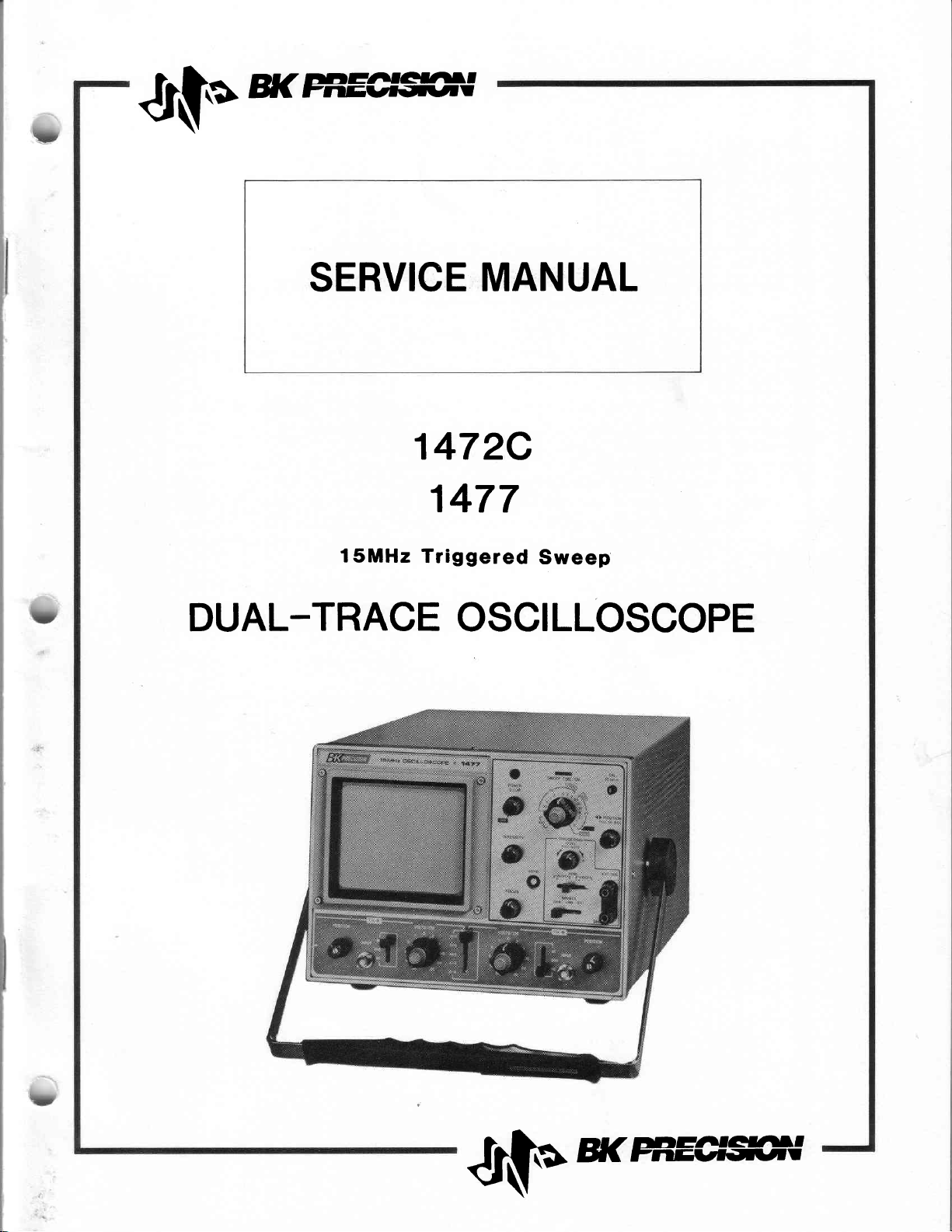
1472C
1477
lSMHz
Triggered
Sweep
DUAL-TRAGE OSqLLOSCOPE
lllronn'
\,\
Bt(
Page 2
WARilI1{G
fhis service mantrcrl
teclnicions only.
yvu
board when tJle oscilloscope is operating. High
present
present
any
turned off.
unit.
t477.
arate schematic is
essentially
pearzrnce
knobs,
1477 is on
qnlified
are
voltage
High
on
the sweep
on the
time the
Always observe caution when
Contacting
This
second edition
Electricaly, Model
apply
from Model
etc.
A
page
To arrcid electnc
to do
up to
power
oscilloscope
exposed high voltage
DIFFERENCE-S BETWEEN
supplied
to both models.
parts
list
34.
is intended
shock,
so.
rfDC
2000
board. Line
transformer, on-off
is
corurected
of the service
1477 is very similar to the
for
l47ZC,
itemizing
using a
present
is
voltage
could
manual is
eadr model.
Model
those
use
for
do
not
on the CRT
of LZO VAC
switch,
to:ur
housing
the
result
MODELS
L477 has several changes
front
new
parts
qnlified
W
perf
orm servrcrng urless
and
voltage up to f95 VDC is
power
and
power
AC
is removed
in
fatal
expanded
Model
The
circuit board
panel,
which are unique
new
electronics
power
(or
240 VAC)
supply
source,
electric
include
to
1472C. A sep-
handle,
supply
board
even if
from
shock.
Model
drawings
in ap-
for Model
is
the
\-
new
\-
Page 3
TABLE
OF
CONTENTS
b
OPERATOR'S
SPECIFICATIONS..............
CIRCUITDESCRIPTION.................
SERVICING
TROUBLESHOOTING
AD
JU
STM ENTS
PARTS
LfST........................
CIRCUIT
PowerSuppIy....................................
Vertical
SweepBoard
VO
LTAGE M
MODEL
I4TZCPRODUCTION
CONTROLS'
...........
. . . .
. .
. . . .
BOARD MAPS
Amplifier
..............
EASUREM
INDICATORS
AND FACILITIES
o.............
f ..... o........
r..........o...............o
. . . .
. . . .
. . . . . . . . .
. .
. . . . .
.
r................
ENTS
. .
o . . . . .
. . . . . . . .
o o........
CHANGES. .
. . . . . .
. .
. . . . . . . .
. . .
. . . .
o. o.......
'.............
o. o. o
. . . . . . .
. . .
o . . o .
. . . .
. . . . . .
o o...........
....7
o.....8
. . . . . .
. . . . . . . . . . .
r r I r..
. . 10
. . 16
..., Z!
...27
... 28
o o..
r.. ...2g
. . . . . . .
. . . . .
. . .
. . . . .
.
30
. 30
3
5
:
MODEL
MODEL
MODEL
MODEL
I47ZC SCHEMATIC
1477
PARTSLIST................
SCHEMATIC
1477
1477
PRODUCTION
RE'ERENCE
I47ZC
L47ZC
Instructiorr Mantral
Composite
(Schematic
L477 Instructigr Manual
1477
Composite
(SchematicDiagram&
DIAGRAMS
DIAGRAM
. . . . . . . . .
CHANGES......
PUBLICATION
.
. . .
...,.
. . o . .
Diagram
o....
. . . . .
&
o o. o. r..
. . . . . . .
o..
o...
. . . o . . . . . . .
parts
List) . . . . . .
partsList)
. . . O''''''
I'''''
I r. '.. o....
. . . . . .
o.......
. . . . . .
o o o.. ..37
S
480-1.82-9-001
499-091-9-001
o...
r... 480-263-9-001
..... o o
499-f60-9-001
31
o o ..34
. . . . 35
U
Page 4
\t
11
10
12
2
2
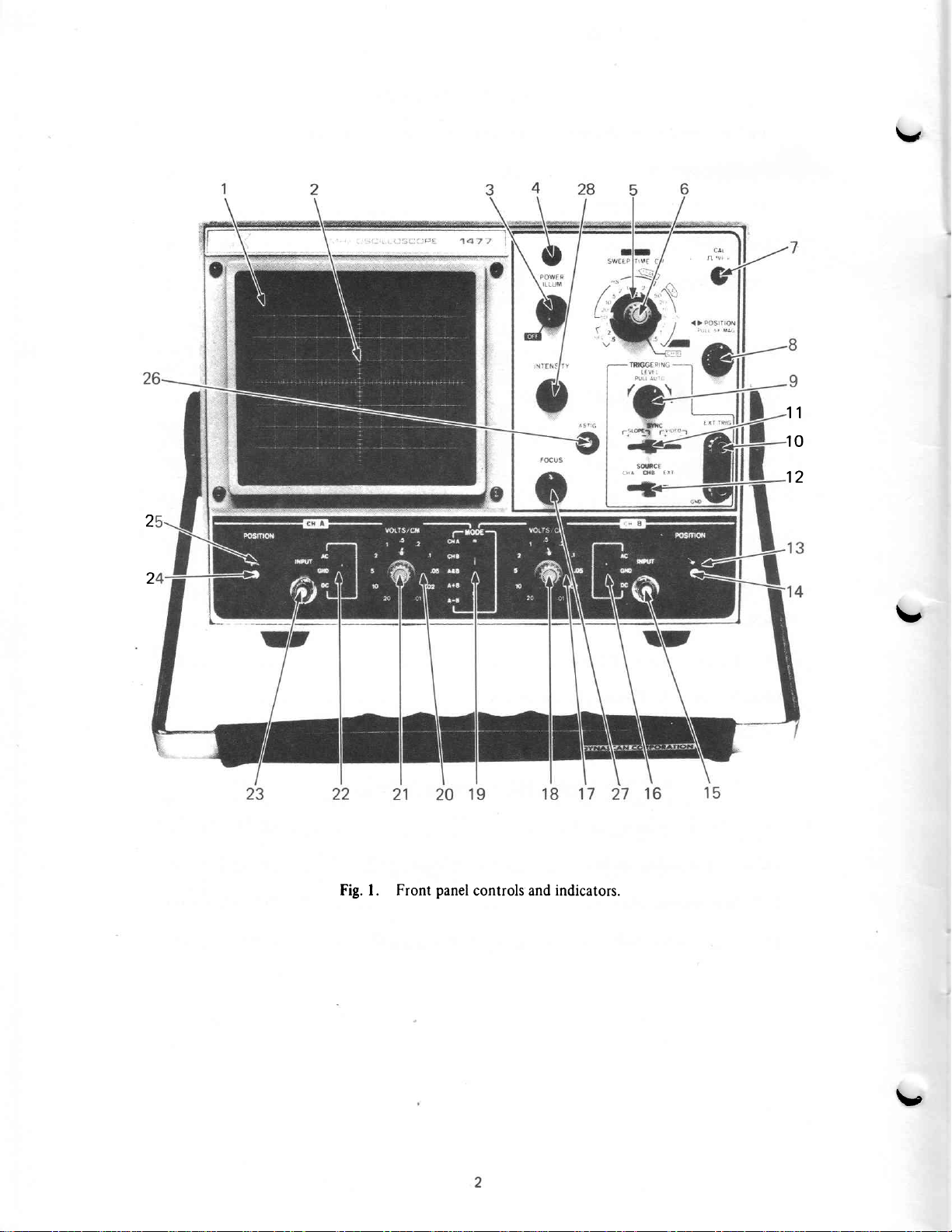
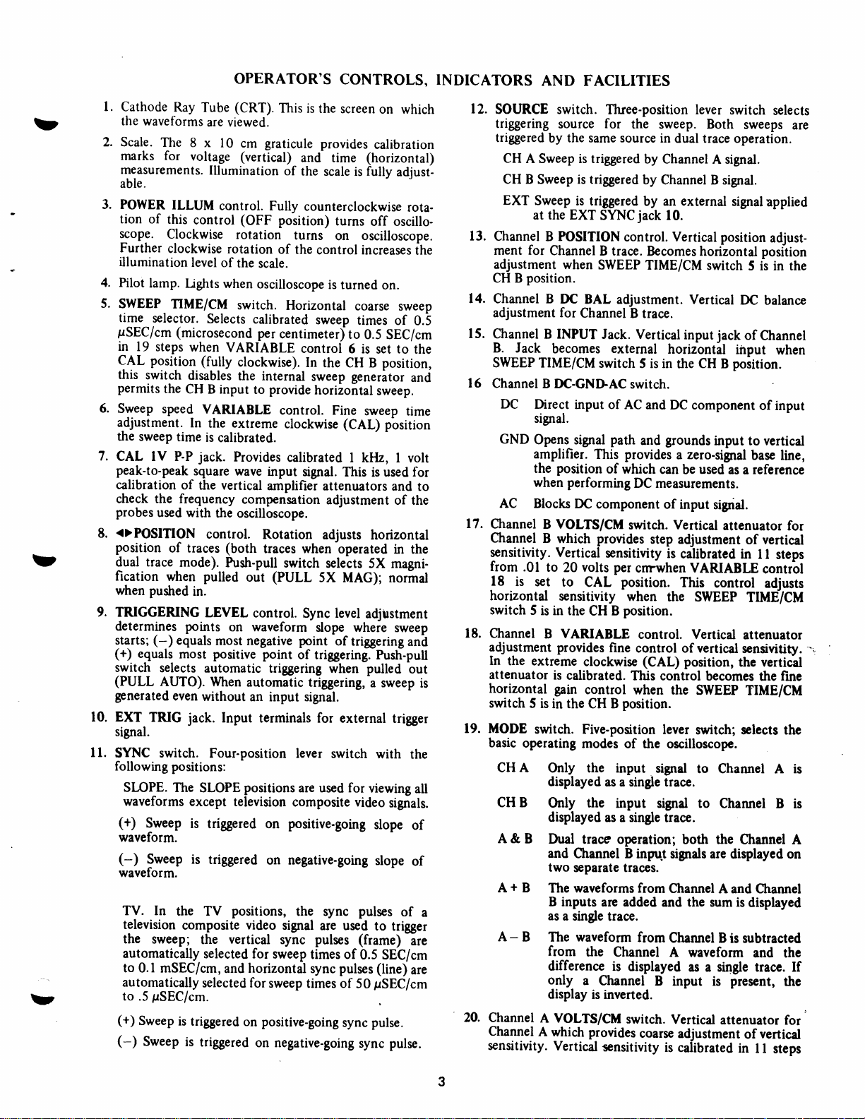
Fig. l. Front
panel
controls and indicators.
v
\,
Page 5
OPERATOR'S
l.
Cathode
U
:
-
the waveforms
2. Scale.
marks for
measurements.
able.
3. POWER
tion
lcop9.
Further
illumination
4. Pilot
5.
SWEEP
time
pSEC/cm
in
CAL position
this
permits
6.
Sweep
adjustment.
the
7.
CAL lV P-P
peak-to-peak
calibration
check the frequency
probes
<>POSITION
8.
position
dual trace
fication
when
9.
TRIGGERING
determines points
starts;
(+)
switch
(PULL
generated
10. EXT
signal.
ll.
SYNC switch.
following positions:
SI-oPE.
waveforms
(+)
waveform.
(-)
waveform.
TV. In
television
the
automatically
to
automatically
to .5
(+)
(-)
Ray
The
8 x
voltage (vertical)
ILLUM
of
this
Clockwise
clockwise
level
lamp.
Lights
TIME/CM
selector.
(microsecond
19
steps
when
switch
sweep
equals
lweep
0.1 mSEC/cm,
Sweep
Sweep
disables
the
CH
speed
In
time
of
used with
of traces
mode).
when
pushed
(-)
equals
most
selects
AUTO).
even
jack.
TRIG
The
except
is
Sweep is
the TV
composite
sweep;
pSEC/cm.
is
triggered
is
(CRT).
Tube
are viewed.
l0
Illumination
control.
control
rotation
rotation
of
the
when
Selects
VARIABLE
(fully
B input
VARIABLE
extreme
the
is
calibrated.
jack.
Provides
square
wave
the vertical
the oscilloscope.
control.
(both
Push-pull
pulled
in.
TEVEL
on waveform
most negative
positive
automatic
When
without
Input
Four-position
SLOPE
television
triggered on
triggered
positions,
the vertical sync
selected for
and
selected for
triggered
This
graticule
cm
of
Fully
(OFF
position)
of the
scale.
oscilloscope
switch.
clockwise).
the internal
comp€nsation
positions
on
Horizontal
calibrated
per
centimeter)
provide
to
control.
clockwise
calibrated
input
amplifier
Rotation
traces when
switch
(PULL
out
control.
point
triggering
automatic triggering,-a
an
input
terminals for external
on negative-going
video
signal
sweep
horizontal
sweep
positive-going
on negative-going
turns
lever
composite video
positive-going
the sync
CONTROLS.
is the
screen
on which
provides
and time
the
scale is fully
counterclockwise
control increases
is
sweep
control
In
the CH B position,
sweep
horiiontal
signal.
attenuators
adjustment
adjusts
selects
5X MAG);
Sync level
slope where
point
of triggering.
when
signal.
switch
are used for
are used
pulses (frame)
times of
sync
times of
calibration
(horizontal)
turns
off oscillo-
on oscilloscope.
turned
on.
coarse
times
to
0.S SEC/cm
6 is
set to the
generitor
sweep.
Fine
sweep
(CAL)
pbsition
I
kHz, I volt
This
used for
is
and
horizontal
operated
5X magni-
normal
adjustment
of
triggering
Push-pull
pulled
sweep
trigger
with
viewing
signals.
slope
slope
pulses
to
trigger
0.5 SEC/cm
pulses (line)
gSEC/cm
50
pulse.
sync
pulse.
sync
INDICATORS
adjust-
rota-
ihe
sweep
of
0.5
and
time
to
of the
in the
sweep
and
out
is
the
all
of
of
of
a
-are
are
12.
SOURCE
triggering
triggered
CH
A Sweep is triggered
CH B
Sweep
EXT
Sweep
at the EXT
13.
Channel
ment for
adjustment
position.
CH B
14.
Channel B
adjustment for
15.
Channel
B. Jack
SWEEP
16
Channel
17.
Channel
Channel
sensitivity. Vertical
from
l8
horizontal
switch
18.
Channel
adjustment
In
attenuator
horizontal gain
switch
19. MODE
basic
20. Channel
channel
sensitivity.
TIME/CM
DC
Direct
signal.
GND
Opens signal
amplifier.
the
when
AC
Blocks
.01
is set
5
the extreme
5
is
switch. Five-position
operating
CH A
CH B
A &
B
A + B
A-
B
A VOLTS/CU
A
AND FACILITIES
switch.
source
by
POSITION
B
Channel
when
DC
INPUT
B
becomes
B DC-GNDAC
position
B VOLTS/CM
B
which
to
20
to
sensitivity
is in the
VARIABLE
B
provides
is
in the CH B
Only the input
displayed
Only the
displayed as a single
Dual
and
two
The
B inputs
as
a single
The
from
difference is
only
display
which
vertical
Tfuee-position lever
for
the same source
is triggered
is
BAL
Channel
input of
performing
DC
volts
CAL
clockwise
calibrated.
control
modes
trace operation;
Channel B
separate traces.
waveforms
waveform
the
a
provides
the sweep. Both
by Channel
by Channel B
triggered
SYNC
B trace.
SWEEP
Jack.
switch
This
component
provides
CH
are added
Channel
is inverted.
sensitivity
by
jack
control. Vertical
Becomes horizontal
TIME/CM
adjustment. Vertical
B trace.
Vertical
external
5 is in
switch
AC and
path
and
provides
of
which
DC measurements.
switch. Vertical
sensitivity
as a single trace.
trace.
step adjustment
per
crnwhen VARIABLE
position.
when
position.
B
control. Vertical
fine
control of vertical
(CAL)
This control
when
position.
of the
signd
input signd to
inpu.t signds are
from
from
Channel A
displayed
B input is
switch.
coarse
in
an external
grounds
can
of
lever
trace.
and the sum is
is
switch
dual trace operation.
10.
input
horizontal
CH
the
DC component
zero-signal
a
used
be
input
is
calibrated
This
the SWEEP
position,
the
SWEEP
switch; selects the
oscilloscope.
to Channel A is
both the
Channel
Channel
waveform
as a single trace.
Vertical
adjustment
calibrated
sweeps
A signal.
signal.
signal
applied
position
switch
jack
B
input to vertical
sigid.
attenuator
control
becomes
Channel
A and
B is subtracted
attenuator
adjust-
posiiion
5 ii in the
DC balance
of
Channel
input
position.
of input
base line,
as a reference
of vertical
in
I I
contrbl
adjusts
TIMETCM
attenuator
sensiviti$.
the verticd
the
TIME/CM
Channel A
displayed on
Channel
displayed
and thc
present,
vertical
of
in
I I
selects
are
when
for
steps
-i
line
B is
If
the
for
steps
Page 6
OPERATOR'S
CONTROI.S.
INDICATORS
FACILITIES
AND
per
from .01
set to the
2l is
21.
Channel
adjustment
extreme clockwise
In the
attenuator
22.
Channel A
DC
GND Opens
AC
Channel A
23.
A.
Channel A DC BAL adjustment.
adjustment
25.
Channel A
for
ment
volts
to 20
YARIABLE control.
A
provides
calibrated.
is
DC-GNIIAC
Direct
input
vertical
base
as a
ments.
Blocks
INPUT
for
POSITION
Channel A trace.
position.
CAL
fine control of
switch.
input of AC and DC component
signal.
signal
amplifier. This
line, the
reference when
DC component
jack.
Channel
A trace.
control.
when
cm
(CAL)
path
and
position
performing
Vertical
Vertical
VARIABLE control
Vertical
vertical
position,
provides a zero-signal
of which can be
of input signal.
input
Vertical
ground
DC
jack
position
attenuator
sensitivity.
vertical
the
of
input to
used
measure-
of
Channel
DC
balance
adjust-
ASTIG
26.
optimum
with
28.
after
FOCUS control.
27.
INTENSITY
28.
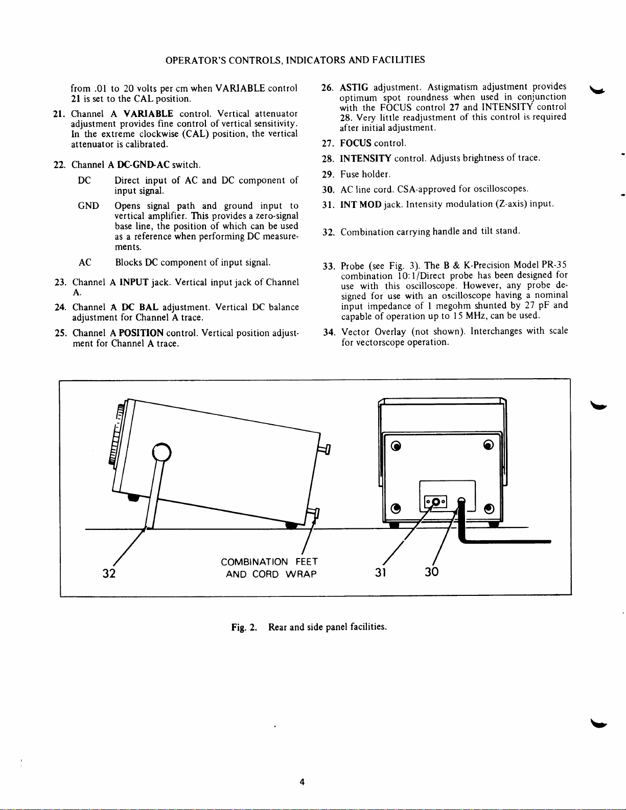
Fuse
29.
AC
30.
INT
31.
32. Combination
Probe
33.
combination
use with
signed
input
capable
Vector
34.
for
adjustment.
spot
FOCUS control
the
little readjustment
Very
line cord. CSA-approved
vectorscope
adjustment.
initial
holder.
jack.
MOD
(see
Fig.
this oscilloscope.
for use
impedance of
of operation
Overlay
roundness
control.
Intensity
carrying
3). The
l/Direct
10:
with an
(not
operation.
Astigmatism
when used
27 and
this control
of
Adjusts
I megohm
up to l5
brightness
for
oscilloscopes.
modulation
and
handle
K-Precision
B &
probe
has been
However,
oscilloscope
shown).
shunted
MHz,
Interchanges
adjustment
in
INTENSITY
tilt
conjunction
of trace.
(Z-axis)
stand.
Model
designed
any
having
by
can be
is required
probe
a
27
used.
with
provides
control
input.
PR-35
for
de-
nominal
pF
and
scale
v.
COMBINATION
AND
Fig. 2.
CORD
WRAP
Rear and
FEET
side
panel facilities.
\,
/
I
30
\'
Page 7
SPECIFICATIONS
(CH
and CH
b
VERTICAL AMPLIFIERS
Deflection
Frequency
Risetime
Overshoot
Input
Input
Tilt
Max.
Operating
Chop
Ctrannel
factor
Response
Resistance
Capacity
Input Voltage
Modes
Frequency
Separation
A
0.01 V/cm
I I ranges
adjustment.
DC:
DC to l5 MHz
AC:2 Hz
24 nanoseconds.
3% or less.
I
megohm
(t3
pF
22
bss than 5%.
alte
rnate
kHz
(DC +
A only.
(dual
(single-trace
(single-trace
of
(n0%')
than
300 V
PP.
Channel
Channel B only.
A & B
matically
times of
selected for
A + B
of Channels
A - B
ference
200
Better
v
SWEEP
CIRCLJITS
Sweep
System
Sweep Time
Sweep Range
Variable
Sweep Magnification
Unearity
Length
TRIGGERING
Source
Slope
Control
Sweep
of
v
Triggering
Range
(Common
of
to
CH A
Triggered
matic
mode,
without
0.SpSEC/cm
(!57")
quence.
provides
At least
Obtained
sweep 5
mum
0.1,/SEC/cm.
3% or
5%
pSEC/cm
102
CH A,
sensitivity.
P
tinuously
pull
2O Hz to 15 MHz
deflection as measured on
ray tube).
input
in 19 ranges,
Each overlapping
for
2.5 times.
times
swee p speed
less
SEC/cm
or less for
mm to
CH
ositivc
for
AUTO.
B)
V/cm,
to
20
providing
each
(-3
dB)
to 15 MFIZ
(approximate).
pF).
chopped at
I mS/cm and
trace
all
A
Channels
60 dB.
(-3
peak)
AC
trace);
automaticallv
faster
sweep timei.
algebraic
B).
and
algebraic
A
trace
all sweep
and
and CH B)
and
automatic. In auto-
sweep is
signd.
to
0.5 SEC/cm
in l-2-5
fine
adjustment.
by enlarging
from
distortion
to
2
pSEClcm
I
ranges.
I l0 mm.
B
and
and negative,
variable
the above
center.
pSEC/cm
EXT:
level
(min.
{%,
for
fine
dB)
or
600 V
auto
slower;
sum
dif-
B).
obtained
se-
range
Maxi
becomes
for
0.5
ranges.
and
0.5
p-p
I V
con-
control;
0.5
cm
cathode
in
TV Sync
HORIZONTAL
input)
Deflection Factor
Frequency Response
Resistance
Input
Input
Capacity
Input Protection
X-Y
Operation
CALIBRATION
INTENSITY
Voltage
Input Resistance
POWER
Input
Regulatron
MISCELLANEOUS
Scale
Mechanical
PROBES
Attenuation
Input
Connector
Tip
REQUIREMENTS
Model No.
Impedances
AMPLIFIER
VOLTAGE
MODULATION
Features
Vertical
separator
any
form
expanded for
and
automatically be
CM switch.
TVV
mSEC/cm.
TVH
and horizontal
circuit
portion
of complex TV wave-
can be
synchronized
viewing.
(frame)
TW
=
=
0.5
pSEC/cm
50
SEC/cm to
provided
sync switched
SWEEP
gSEC/cm.
(Horizontal
l0
mV/cm
DC to I MHz
I megohm
(t3pF).
pF
22
(DC
V
300
input thru
(nominal).
(-3
dB).
(nominal).
+
peak)
AC
p'p.
With
SWEEP TIME/CM
position,
CH B
the
CH A input
becomes the Y input
and
the
X input
position
horizontal position
I kHz
input
CH B
(horizontal).
control
becomes
control.
square
wave of
becomes
(!s%).
p-p
2O
minimum
470 kO
120
(3-wire
for oscilloscopes.)
108
Variable illumination.
Carrying handle for
PR-35
Combination
l0:l = l0
Direct = I
BNC
Spring-loaded
(nominal)
VAC,
line
132 vAc.
to
(two
megohms, l8
megohm, 120
!2Vo
,
tlz,23
50/60
CSA-approved
cord,
tilt stand.
required).
l0:l
and direct.
hook-on tip.
so that
(line)
TVH
TIME/
to
CH B
or
600 V
switch in
(vertical)
The
CH B
I V p-p
watts.
pF.
pF.
sync
and
0.1
0.5
the
the
Page 8
s!
-[
F-
!d
(f;
5r
JC
<tg
3dr
E5d
yoi
=qH
(Fl
=gt
<!lo
5:r
<oo
14 |
ood
jd.
m)lo.
-T('G
;'i: d
F
o
v<
>?
2-
@=o
-\F
35;
2a
ir
-tt
cJ
:i
ICr
o(L
v.
J
Fl-uJ
z)i
.|c=
F.J
i
ao>
o(
?
as
FU
Z-t
od
!>
c(
a1 UJ
Ycr
-0-
(IF
r!<
1t
>
aO
trJ
r!F
\z
oo
tr-
O
tJ.F
lrr
F
z
J
C
(J
o'.r|
o6
JZ
o(
IA
F
Y
tz
a<
UJ
o
f
.z)
lJ.
11n
FM
rr,l
{ -
Oc(
Ou-
54(J
"o
c>
J
trJ
r-
5ee_,
a;;
Ug
(O
^r
*
2".
ias
JA
IJ(J
9oH
a;H
lrJ
O
az
a<
FI
vl
F
FUJ
z
@
I
X
E-l
5e
a
s>
trJ
>o
?c
YJ
BU1
J
q')
(J
.tt
()
(n
q)
O
F
e.l
r-
:v
q)
oo
cO
E
.Y
()
c/)
Eb
TI
3r
E!
y1
;i
F
(a
TZ
o-
j
3r
Eq
,r7,
OF
Ik
frrI
;'il
F
o.C
trt
E
(>
uz-
3o
i^z
(
(r?
oi
eki
;ll
ulF
|,'
b
6
Page 9
CIRCUIT DESCRIPTION
v
:
U
The
down of the
reference to the
GENERAL
Basically. the oscilloscope
vertical preamplifiers,
network.
switched, as
type of switching of the
determined by the position
MODE
arnplifier
which drives
Horizontal
amplifier.
calibrated
preamplifier when X-Y
B
All
supply
converter
the CRT.
VERTICAL
Channel A
circuitry and circuit
The
section of
100: l, 1000: l. The second section
5:
and
provide
The
sistors
FET's
amplifier
VRl0l
an internal
applied
is
the output impedance
Ql06
I
the
12
control
provides
across
'the
emitter circuit
correct
ments.
The trigger amplifier
the emitter of Q 108 and
a
tne signal
The only
amplifiers
the CH B
MODE LOGIC
The
B)
is controlled
Dl08
When
which
DlOl and
vertical
diagram, Fig.
block
oscilloscope.
schematic
each having
The outputs
desired,
OPERATION
of
feeds
the
deflection
Drive
sweep speed circuits
voltages are fully
provides
PREAMPLIFIERS
and
vertical
the
The
l.
and
in
combined
vertical
the
vertical
and
Ql02
the
and
Ql02
pair
the front
is
balance
to
emitter
Q107.
and I
adjusts
a DC
screen. Amplifier
deflection factor
to the trigger
difference between
is that the
signal when in the A-B
mode
of operation
each
of
CH
A is selected,
reverse-biases
D104, allowing the CH
amplifier.
of the
into the
VERTICAL
the
vertical
to
attenuator
preamplifier
with output
/5
the
deflection
the
horizontal amplifier
regulated 2kV
a
Channel B
operation
attenuator
attenuator
Ql03
Ql03
panel
control. The output
followers
to drive conventional
VRl05
attenuator
gain
component
of
Q
circuits.
MODE switch
ICl0l
by
the
channel
D
I 02 and
At the same
3, outlines
Circuit details are obtained
diaeram.
consists
its
vertical preamplifiers can be
main vertical
CH A and CH B
of the
LOGIC. The
OUTPUT AMPLIFIER,
plates
provided
is
or by the signal
operation is
regulated
accelerating
preamplifiers
the same
is
has two sections.
provides
effect of the two sections is
ratios in a l-2-5 sequence.
consists
transistors
and
form a balanced
signals
DC balance control
104 and
Q
VRl06
and
positions.
of
Ql06
move the
to
gain
is
and
Ql08
for accurate
l9
I
and
Q
109 and
Q
position.
(CH
the
CH B,
A,
ICl02 and
and
preamplifiers.
output
D 103 and
time ICl02
the
circuit
of two
own
MODE
of the CRT.
by the horizontal
selected.
ratios of
provides
of
opposite
of
of
Q
are
and
Ql07
adjusted
Ql09
I 20 amplifies
provides a portion
CH A and
reverses
of IC 102
A signal into
attenuator
input
amplifier.
preamglifiers
switch
main vertical
is furnished by
from the
DC-to-DC
and a
potential
contain identical
for both.
The first
l: l, l0: l,
ratios
FET
input
thru
Ql04
differential
and
102 and Q 103
Q
which lower
105
amplifier stage
balance
VARIABLE
The
while
trace
by
provide
to
voltage
CH B
polarity
the
A & B,
A
diodes
Pin 3
forward-biases
Pin I I
break-
by
identical
The
and
CH
to
of
2: I
to
tran-
Q109.
polarity.
VRll2
pots
for
VRl0l
vertically
VRl07
the
measure-
the signal
pre-
+
B, A
Dl0l
low,
is
main
the
output is
which forward-biases
high
D 105
biases
main amplifier.
selected, both channels
is
a rate equal to
at
(200kHz).
simultaneously
operation is
switched
is
VERTICAL
The selected
to the vertical
ICl03.
amplifier.
The output
Q306
the
drive
TRIGGER CIRCI.IIT
The trigger
SW20l.
amplifier
amplifier
thru
fed
of the SWEEP TIME/CM switch
SYNC
Transistors
differential
a
as
emitter follower
Q203
SW202, r or
DC
level
of the
When
routed
Q205
cutoff
corresponding to
Positive-going pulses
of
Q205
video signal.
in
of
of
-
-
When
SEC), capacitor C2O7 is switched
horizontal
the
The trigger
the SCHMITT TRIGGER
IC20l. The output
SWEEP CONTROL
the clock waveform,
Q2l3
Transistors
resistors
and
MILLER
a
voltage.
to the RS
transistor
As soon
lC2O2
until
on and
terminates
and
For CH
For
A + B and
applied to the main
selected,
to the horizontal
AMPLIFIER
signal
amplifier which consists of
The signal
where the
AMPLIFIER
depending
TRIGGER
and
by
to initiate
is held low
the
amplifier
vertical deflection
Selecting
transistor switch
to the
The
sets
signal is
source, either CH
Qll9
and
Ql2l
Q20l , Q202, Q203,
-
respectively.
to
the trigger
TV+
e1 TV-
SYNC SEPARATOR circuit
Q206.
the
corresponds to the
in TW
sync
signal
to sweep.
Q2l6
selected by the
INTEGRATING circuit
sweep ramp
flip-tlop
I and
Q2l
as the
sweep
ramp
pin
l3
the
sweep.
D 106 and
prohibiting
D 108
CH
and
amplifier.
Q20l
upon
LEVEL
Q205
negative
an average
positions
Q
by
of
the reverse is
B,
are alternately
the
chopping
A B, both channels are
CH A is
amplifier.
from
level
Ql2O
Q122.
AND
drive
pulses.
passes
pulses
flip-flop 1C202. On the negative edge of
the
and
consisting of two
Q212.
output of'lC2O2
Q2l
is
lC2O2 LOW which
preamplifiers
the
is increased to drive the output
consists of transistors
amplified
plates
A as
the
and
trigger amplifier selected is
The
Q219. Q2l9
except
INVERTER
The
and routed to
position
the
Emitter
signal depending
control.
selected, the output
is
biased
is
voltage
value
Q205
qync
of time base switch
thru emitter follower
circuit consisting
from
output
Q
Q2l6
SWEEP TIME/CM switch
from
the collector of
I to
exclude any
terminated.
D 107 and
CH B signal
true.
switched
oscillator frequency
amplifier.
turned
of the CRT.
A or CH B,
trigger
near cutoff.
out of cutoff.
and
on and
to the levels required to
source
CH B enables
on in all
is
CH B.
and
Q204
signal is applied to
the
of the
follower
upon
developed
of the
tips of
in
by
Q206
IC20l
PIN
goes
the timing capacitors
provide
to
gates
goes
Transistor
turns
from the
When
by
When
CH B is
then
is
Ql23,Ql24
Q30l
selected by
is
enables trigger
positions
are connected
base of
low,
from
new
Q202
SYNC switch,
Q2O+
position
the
of
consisting of
Q205
across
input signal.
The
the
composite
(.lmS
to filter
Q207
of two
8
clock the
turning
linear ramp
a
Q2l7
IC20l
low, the
clock
Q2l2
Q2l3
reverse-
A & B
ICl0l
X-Y
applied
and
thru
trigger
or
adds
a
is
Q203
is held
Q205
output
.5
to
out
and
gates
of
off
form
fed
is
thru
reset of
pulses,
turns
and
on
Page 10
CIRCUIT
DESCRIPTION
\r.
Transistors
TRIGGER
is
adjusted
and
condition
reset
9qlqryin.d
TIME/CM
Q9
of
produce
is applied
1C202
Q208.
SENSE
so that the
switch.
by
allows
the
switch.
pulses which
QlC|().
to the RESET
resistor
and
When
slope is
a
High
power
voltage
Line
transformer,
the
turned
from
in
fatal
the
not
keep
sweep to recirculate
and
capacitor
voltage
supply
up
to 195
voltage
oscilloscope
off.
the
unit. Contrcting
electric
fornr
Q2l0
TRIG LEVEL
triggered.
of IC202.
up to
board when
of 120
on-off
Always
transistor
Q2tO
A low
selected by the
2m0
volts
VAC
switch,
is
connected to
observe
shock.
the
AUTO
control
ON. The
Q8
on
rhe
on
at a rate
SERVICING
WARNING
volts
the
DC is
lor
and
caution
exposed high
present
DC is
oscilloscope
present
24O VAC)
on the swe€p
power
AC
an
when
The sweep
the
input of the
Q220, Q22t
When
mode, transistor
B signal
The output
horizontal
on
is
operating.
present
is
supply
power
souroe,
the housing is removed
voltage
ramp from the
-
Q225
in the
is
applied
of transistors
deflection
CRT
the
board.
the
on
board
any
even
result
ould
horizontal
CH B
Q2
to
and
High
power
time
collector of
.
t g is turned
Q220
plates
if
amplifier consisting
position
and
Q224
of the CRT.
Q2l7
of SWEEP
off
to the horizontal
and
TIME/CM
thru IC203
is
QZZS
applied to
is applied to
of
Q218,
switch,
and the
CH.
amplifier.
the
\,
HOUSING
Remove five Phillips head
1.
each side, onc
tom of
2. Slide
through the
CRT
WARNING: Keep
socket.
Remove
1.
REXIOVAL
from
houring.
complcte oscilloscope chastis
front
of
TILT
hands
High voltage
housing.
screws,
top, and two
housing.
the
from
away
(2000
VDC)
from
one
from
out
CRT
present.
bot-
Loosen the tvvo screws
2.
around the
Turn on
3.
to obtrin a
4. Grasp the CRT
shicld toward
the
rotate the CRT so
horizontal line on the
a
Tighten
5.
trace
neck
the oscilloscopc
single trtce.
through
the CRT band,
remains
horizontal.
of
the CRT.
front
the
the tracc
which
clamp the band
diust
rnd
fingpr
the
of the
is
grrticule.
making
controll
holes
CRT and
parrllol
sure that
in
with
the
b
Page 11
SERVICING
v
230 VAC OPERATION
l. Remove
Remove voltage
2.
3. Rotate
4. Replace
Replace
5.
housing from
selector
plug 180"
and
0.7A fuse
housing.
scope.
re-insert
with
0.3A fuse.
plug
(see
plug.
Fig.
8).
2.
Lift off
Reinsert
3.
panel
graticule
graticule
from bezel.
on
mounting holes.
bezel and
snap
bezel
into front
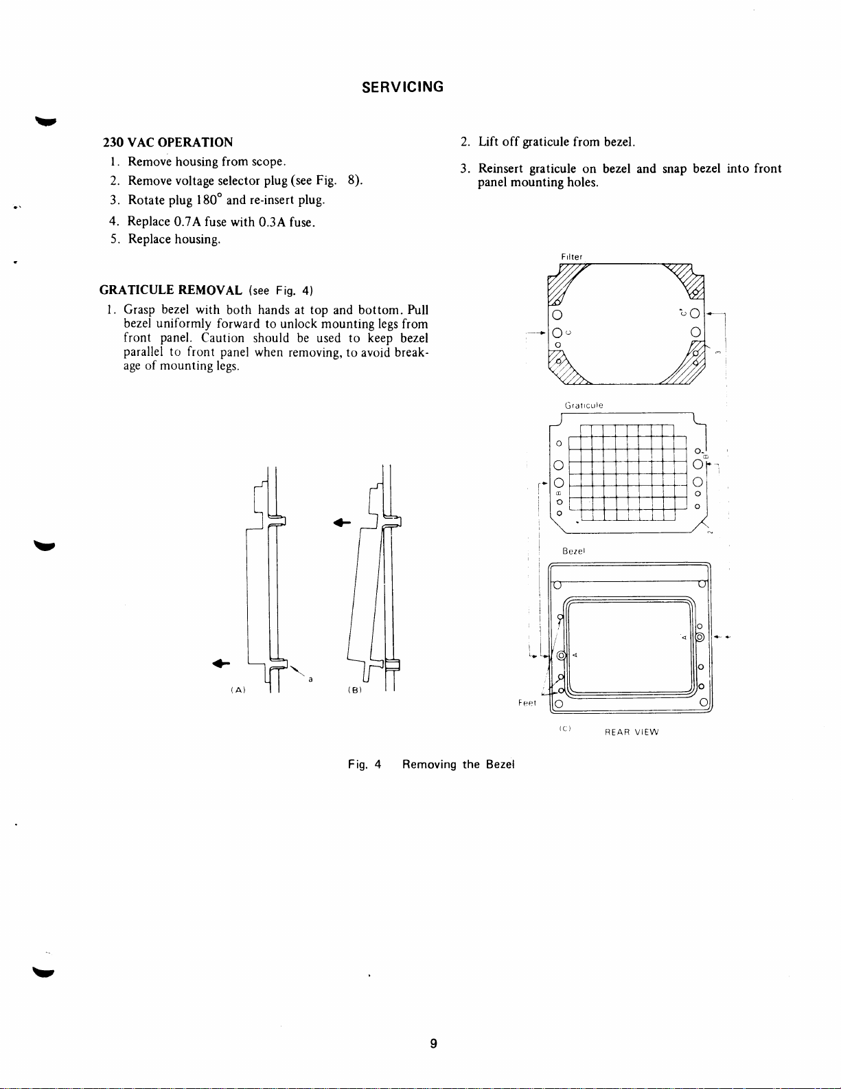
GRATICULE
REMOVAL
l. Grasp bezel with
bezel uniformly
panel.
front
parallel
to front panel
age of mounting
Caution
(see
Fis.
a)
both hands at top and bottom.
forward
to unlock mounting legs
should be used
when
removing,
to keep
to avoid
legs.
Pull
from
bezel
break-
o
O,,
o
o
?,c
O
I ll
\-/
.)i
vl
ol
ol
a
I
I
I
v
REAR VIEW
Fis. 4 Removing
the
Bezel
v
Page 12
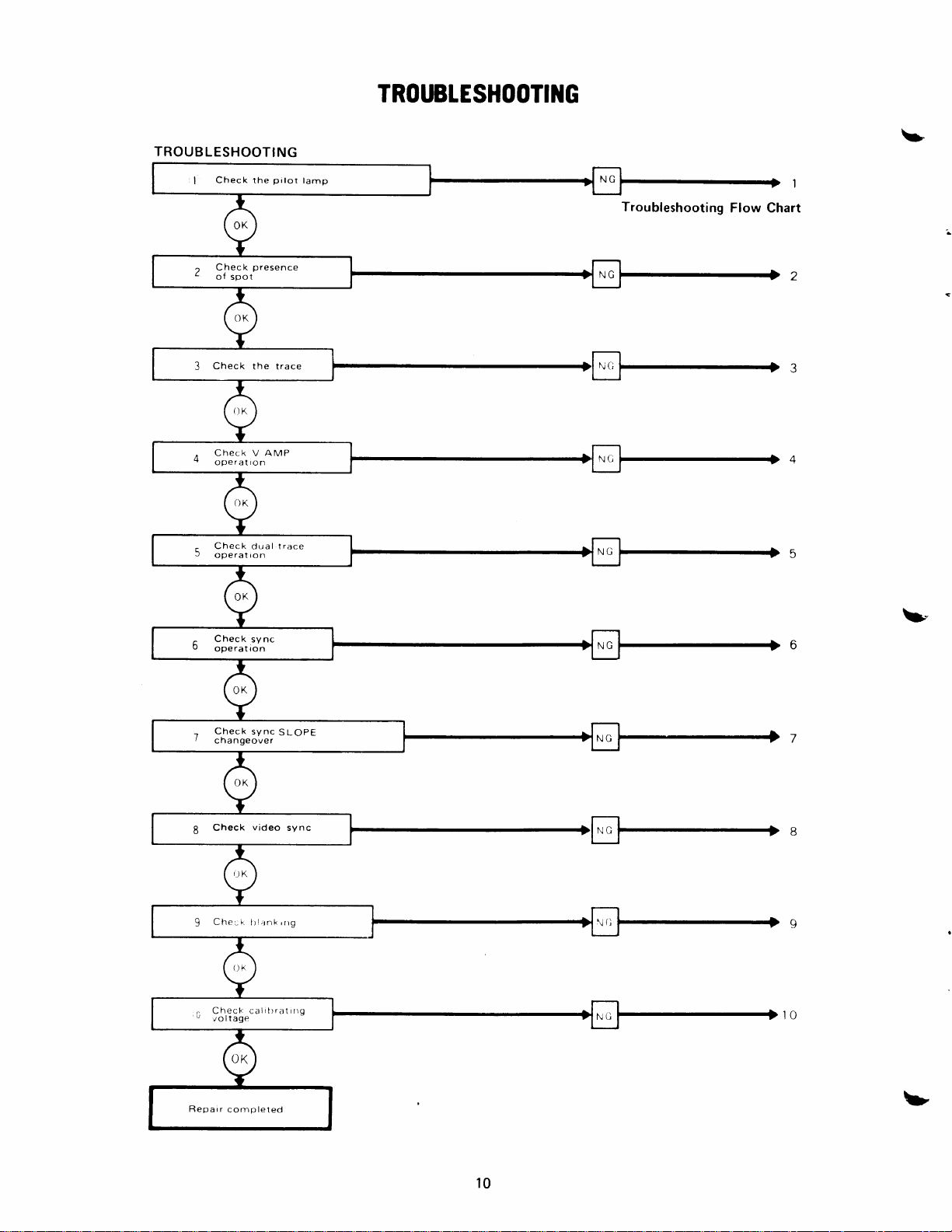
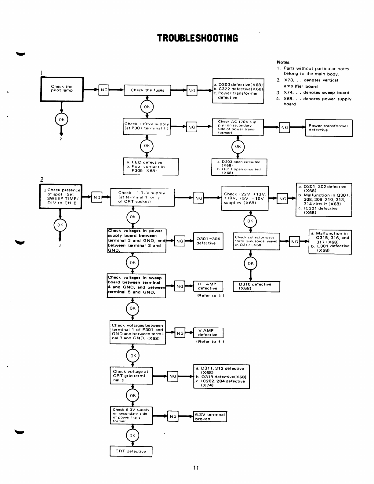
TR0ttstEsH00Trl{G
TROUB
r
I
2
'
3
LESHOOTI
Check the
Check
ot spot
Check the trace
Check V AMP
operat
Check
operat
NG
pilot
presence
ron
trace
dual
ron
lamp
Troubleshooting
Flow
b
1
Chart
Check
sync
ro
operat
n
Check
,
/
6
"
v
sync
changeover
video
Check
Check calitrralrnq
roltaqe
b"
SLOpE
sync
Bepair
comoleted
Lt
10
Page 13
TRottrEsHo0Trltc
Y
Notes:
Check
pilot
the
lamp
Check the
heck
(at
P3O7
a. LED
Poor
b.
P305
+
195V
terminal I
defective
contact in
(x68)
fuses
suppty
Parts
1.
without
belong
a.
D3O3
b.
C322
Power
c.
def ec t ive
defective(
defective(X68
transf
X68)
ormer
2.
3.
4.
. .
ampllfier
X74.
.
X68.
. .
X73.
borrd
Check
AC lTOV
(on
)
ply
side
f
ormer
a.
D3O3
(x68)
b
031l
(x6a)
ol
)
secondary
power
open
crrcurted
open
crrcurted
sup
lrans
to
the
denotes
board
d€notes
.
denotes
particular
main
sw€€p
power
Power
defective
notes
body.
vertical
board
supply
transformer
Check
2
of spot
SWEEP
DIV to
presence
(Set
TIME/
CH B
Check
(at
terminal 1
ot CRT
-1.9kV
socket)
supply
or
2
+22V,
Check
+1OV,
+5V.
supplies.
(
X68)
+
13V.
-1OV
a. D3O1.
b.
c.
Check
collector
(X68)
wave
wave)
-306
v
terminal
end
mlnal
Check
terminal
GND
nal
2
trrminal 3
rd
bctwecn
GND,
5
voltages
and
3 and GND.
and
GND,
trrmlncl
and
and GND.
between
1
P3O1
of
between
(X68)
and
and
termi-
a
o301
def ective
.AMP
H
def ect ive
(Refer
V-AMP
defective
(Refer
to
to
(srnusordal
lorm
rn
0317
D31 O def ective
(
x68)
I
)
{
}
3O2 defective
(
x68)
Malf
unction in
308,309,310,
314 circuit
lC3O1
(
x68)
(X68)
defective
a. Malfunction
0315,
316,
(X681
317
defective
L30l
b.
(
x68)
Q3O7,
313,
in
and
a.
voltage
Check
grid
3
6.3V supply
power
termi-
trans
CRT
nal
Check
on seconctarY
of
former.
at
stde
D311,312defective
(
x68)
b.
0318 defective(X68)
lC2O2,204
c.
(x741
6.3V
broken
terminal
defective
v
C RT
def
ective
11
Page 14
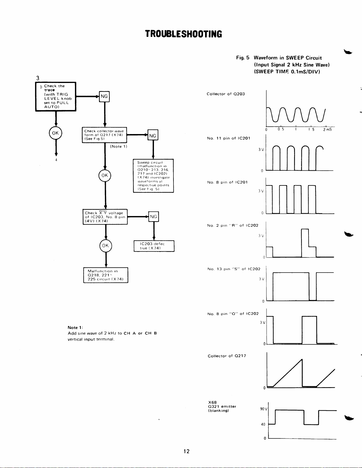
TR0rtsrEsH0oTtltc
Check the
Jr
.-
trace
(with
TRIG
LEVEL knob
PULL
to
set
AUTO)
Check collector wave
form
(See
F ig
Check
lC2O3, No.
o{
(4vl (xt4l
4217
ol
5)
X Y voltage
(X74\
8
pin
Srveep crrcuit
(
malf
u nctron
C)210-
213,216,
217
and lC2O2l
(X74)
rnvestrgate
yJavelorrns
respectrve pornls
(See
lC203
tive ( X 741
F rg
al
5)
defec
Fig. 5
Waveform
(lnput
(SWEEP
corrector of o2o3
Signal 2
Tf ME
I
in
SWEEP Circuit
kHz
Sine Wave)
0.1mS/DlV)
W',
pin
b
No. 11
In
No.
8
No.
2
pin
pin
of
of
"R"
lc2o1
lC2o1
lC2O2
oI
|
':l
lllI
I
:l
,'l
lll
I
n
n
11
b'
Note 1:
Add
sine
vertical
Malfunction in
0218, 221
circuit
225
wave of
input
2
termtnal.
(Xl4l
kHz to
AoTCHB
CH
pin
No. 13
pin
No. 8
lector ol Q.217
Cof
x68
emitter
1
O32
(blanking)
"S"
"O"
of
lC2O2
oI
,,1
lc2,2r"l
40
I
t-l t-
n
,A
t'
0
12
Page 15

TRoltsrESHooTrlrc
v
inPut
vertical
B
or
Note: Add
Check V-AMP
ton
operat
Check
duat
race
t
operat ion
wave
srne
terminal when
kHz
ol 2
checking
toCHA
items
Either
CH
in trouble
Both
CH
in
trouble
Check
CHOP
(with
tion
TIME/DlV knob
to
O.55-1mS).
A or
A,
No.
4
CH
CH B
opera-
SWEEP
ser
-
CH
(except
9
No.
8).
circuit ooera-
Check
tion of CH
f
c101,102, D111-
113 defective
Malf
124 and
unction
lC103
A(org1-1
in
g
(X73)
O123
(X73i
a. lC2O4
(x741
b. lC102
(
x73)
defective
defective
CH 1
CH2:
: Malf
unction
-109.
(x73)
Malfunction
-1
18, D105
(
x73)
D101
in
0101
-
104
in
O11O
-108
v
Check
ALTER
tion
TIME/DlV
to
O.5mS-O.SuS.)
ALTE
R in
a
operat
on
(with
swEEP
knob
0.5mS
opera
ser
(SwEEP
(SWEEP
Poor
S2O3a
TIME/DlV
TIME/DtV
contacl
1 mSl
O.1
(X74)
mSt
-
0.5
b
Fig.
mS
6
Waveforms
at
No.
1
Pin
of P1O2
(X73)
13
Page 16

TROIBTESHOOTIlIG
b
Check
sync
operat ion
Check
nc
5y
EXT
Check
collector.
waveform of
(x74)
0203
waveform
Check
No.8 and
pins
Check waveform
No.
pins
lC2O1(X74}.
o{
8 and
lC2O1(
ol
No. 1
No.
1
'l
1
X74)
-203
o201
def ect
ive
lx74l
at
at
O2O7 defective
(
x74)
lC2O1
defective
1X741
b
INT
Check
(with
switch set to CH A
or CH
Q121, 122
def ect
(x73)
MODE
B)
ive
sync
01
19,
def ect
(x73)
120
ive
14
Malfunction
O2O8,
2O9
(x74)
2to
waveform
Check
at collector
(
X74)
0219
Poor
contact in
(x74)
s201
and
of
in
a. Ol 19,
b. 0219,220
120.121.
122
def ective
(x73t
defective
(
X
74)
L
Page 17

TROIBTESHOOTIlIG
v
Check
6
SLOPE
ove
7
r
Check
sync
sync
change
video
Both
TV
TV.H
defective
Either
TV'H
or
ective
def
TV,v
Malfunction
5202
(x741
V
circuit
in
0206
(short)
defective
1X741
Malfunction
O2O5.
circuit ( X74)
02O6
(openl
and
206
defective
(X74)
in
Note:
Add
v
compotit€
video
rignrl to
vortic.l
input
trrminol.
waveform
Check
form
brating
a9e
wave
ol cali.
volt
Check
at
tc2o4
Check waveform
at emitter
o321
pin
No. 3
(x74)
(X68)
(See
R359 broken
(
x68)
Malfunction
4214,
21
5, and
(x74t
rc203
of
of
in
Fig.
5)
lC2O4
(x74)
a.
0319
dsfectivc
b.
O321
(x68)
defective
and
32O
(X68)
delective
v
Repair
completed
l5
Page 18

AD'USTME]ITS
\
High
voltage
the
CRT and
oscilloscope
volts
DC is
voltage
the
supply
ed
Always
moved
voltage
TEST
Minimum
Sine
constant
cision
or
Sine
stant
Precision
of 120 VAC
power
transformer,
board
to
an AC
observe
from
could result
EOUIPMENT
Requirementr
& Square Wave
voltage
Model
Model
3010 or 3020 Function
Wave
Generator,
voltage
Model
WARNING
up
to 2000
power
is
operating. High
present
any
time the oscilloscope
power
caution when
the
unit.
volts
supply board
on the
(or
240
on-off
source,
Contacting
in fatal
REOUIRED
Generator,
over
tuning range
E3108
output
Sine/Square Wave
1 MHz
over
tuning range
8200D)
present
DC
is
when
voltage
sweep board.
VAC)
switch,
even
the
electric
is
if
turned
housing
exposed
shock.
20 Hz
(B
up
present
and
to 1 MHz,
& K
Generator
Geneiator)
to 15 MHz,
(B
the
to 195
Line
power
is
connect-
off.
is re-
high
Pre-
con&
K
on
on
DC
Voltmeter
meter,
ranges
1%o
(B&K
Frequency
(any
MHz
1o/o
dccur?cy
accuracy
Precision
Counter,
B & K
Precision
at
.1To
Desirable
Oscilloscope Calibrator,
levefs
and 50
Marker
vals
1%
of
accuracy at 50
peak-to-peak
V
Generator, accurate
0.1
mS,
10 uS and
of
Model TG501)
PRELIMINARY
Observe the
1. The items
before
it
source
probe).
following
shipment.
should
voltage
PROCEDURE
before making
given
below
Should
performed
be
(no
or better.
1 kHz,
Model
100 mV
2830)
or better
Frequency
accuracy
Counter)
calibrated square
mV,
(Tektronix
time
0.5 uS
pre-adf
are
re-adiustment
after
adfustment
V,
0.5
Model
marks
at
(Tektronix
adjustments:
usted
calibrating
is required
AC Volt-
to 100
15
to
wave
V
5
PG506)
inter-
at the
be
the
V
factory
required,
power
on the
t
16
L.
Page 19

ADJUSTME]ITS
2. All
v
3. A
I
v
4.
CH
l.
2. Adjust
3. Rotate
4.
I
12
l.
2.
adjustments
resistors
cuit
blade
circuit
removing
For
up
A
AND
Adjust
cH
or the
board. For
screwdriver.
high
voltage
board.
the
optimum
the
oscilloscope
CH
controls to
B).
CH A or
vertically
trace
the
to maximum
lf
the
trace
performing
(front
vertical
while
& I
Position
B, with
panel
movement
performing
ATTENUATOR
/5
trace
V
ATTENUATOR
GND.
Switch to
VRl08(CH
should
trimmers
(about
Be
bottom
adiustment,
B
DC
BALANCE
be made
adjustment,
2000V)
sure
to turn
cover.
sufficiently
obtain
CH B POSITION
the
on
CRT.
VARIABLE
while
CW
control from
observing the
moves vertically
STEP
3,
adjust the
screwdriver
of the
STEP
3.
BALANCE
to vertical
V/CM
.02
B)
until rrace
center
and
is
with the
mounted
turn the
a horizontal
on the
use a
well-insulated
present
is
power
the
power
before
conrrol ro
trace.
more
than 5mm
CH A
or CH B DC
adjustment)
trace
does
not
of screen
V/CU
in .01
VRl05 (CHA)
adjust
vertical
at
cenrer.
semi-fixed
printed
on the lower
off
before
on and
starting.
(CH
trace
cenrer
maximum
so
that the
exceed 5mm
CH
A
or CH
and
input
cir.
flat-
warm
A
or
the
CCW
while
BAL
at
or
3.
Switch
VR
VERTICAL
to
(CH
109
ATTENUATOR
(VOLTS/DIV)
l
Remove
2. Connect
wave
3. With
TC101
board
4.
Successively
adfust
TCll1
PROBE
the
a 1 kHz
signal
VOLTS/DIV
(TC107
until
the
for
CHB) in the
AND
MENT
1.
Set
VOLTS/DlV
2. Set
INPUT
to the
square
ed
and
probe
the
terminal.
probe
waveform.
to 111O,
input
capacitance
V/CM
and
,05
B) until
trace
adjust
is at
vertical
ADJUSTMENT
case.
(output:
generator
set to
forCHB)
optimum
change
trimmers
INPUT
to
and
but input resistance
square
the range
TCl03
CAPACITANCE
to
0.01V.
10: 1 and
Apply
adjust its
In this
mV to 100
50
to the
0.1V, adjust
on the
wave is
and TCt05
same manner.
connect it
a I
kHz
trimmer
case, input
is reduced
VRl06
vertical
lower
obtained.
to
lV
square wave
for
voltage
is
increased
less
to
(CH
center.
p-p)
V
input
terminal.
the
trimmer
printed
and
lOV,
(TCl0g
ADJUST.
to
vertical
the
the
optimum
is
attenuat.
to
than
A)
or
square
circuit
and
and
signal
lOMQ
18pF.
CRT
CENT ADJ.
@
Tpt02
"xill';,
iitr;9,.
@
VRl
IO
GAIN
@
@
TC114
VR111
@
ADJ.
Pi?[
ADJ.
X
GAIN
ADJ.
ATTENUATOR
DC BAL
ADJ.
@u^114,
@
rPlot
$*,
VRl06
I
t
i
v
Fig.
Lower Printed
'-
FRONT
I
PANEL
Circuit
(SACK
^@
_g^^rclol
rrcl03
100
TC104
VIEW)
Board
1
10
@@@'*
TCIO2 TC106
(Vertical
(h
riros
1
Amplifierl
17
Page 20

ADJUSTMEI{TS
\-
3.
Set VOLTS/DlV
(TC108
1O2
board
so that optirnum
4.
Adjust
TC112 tor
rnanner.
the trimrners TC104
VERTICAL
1. Remove
ed
2.
Set VOLTS/DlV to
clockwise
Apply
3.
r nput.
4. Adjust
CHB)
div
the case according to the
for
REMOVING THE
0.05V
VR107
on
of vertical
to
0.1V and adjust
for
CHB)
SENSITIVITY
to CAL.
p-p
GAIN ADJ
lower
the
amplitude.
on
CHB)
in
the 1V
the
square wave
arrd 10V ranges
ADJUSTMENT
CASE.
0.01V and turn VARIABLE
square
wave signal to the vertical
printed
circuit board to
lower
TC106
arrd
procedures
(VRl10
the trrmmer TC
printed
can be
GAIN ADJ
circuit
obtained.
(TC110
in
the
same
describ-
obtain
arrd
fully
for
5
POWER
CRT CENTERING ADJUSTMENT
1. Short
2.
the test terminals TP101
printed
With a horizontal
VR114 on the same
bright
circuit board.
lirre is
bright
centered.
line
printed
TPlO2
and
displayed
circuit board until the
FREOUENCY CHARACTERISTICS
OVERSHOOT
1. Apply a 100
rise
characteristic to
Adjust the
2.
ing)
with
Adjust
3.
tion) with
Adjust
4.
TC113 on the
CHB
SUPPLY BOARD
ADJUSTMENT
kHz square
middle range
TC301
high range
the
VR305
high range for
the
TCl14.
with
input.
the
of
rear
the
on
of
on the same
printed
lower
wave signal
the
square wave
printed
the
square wave
printed
each channel;
circuit
the lower
on
in
CRT,
adjust
AND
having
circuit board.
circuit board.
for
board,
good
a
(after
(rising
CHA
and
with
ris-
por-
for
It
ROTATE PLUG
CHANGE VOLTAGE
240
I
20
TO
VAC
VAC
Fis.
FUSE O 7A_ 1
o
Rear
8.
20 VAC
34-240
Printed
vAC
Circuit Board
TOP VIEW
{Power
Supply)
VR 3O5
TC
301 - MID FREOUENCY
TC
3O2-UNBLANK
VR
3O5-HIGH FREOUENCY
VR
VR
VR
VR
306-r
3O7
3O8-Y
309-
9kvADJ
_
INTENSITY
DEFLECTION
1
ADJ
95V
ADJ
L.,
18
Page 21

AD'USTME]ITS
Table
SWEEP TIME
AND
BRIGHT LINE LENGTH
1.
Remove
2.
Set SWEEP
fully
clockwise
,
I
V
3. Apply
sisnal to
the
waveform
point
4.
Adjust
within
sinusoidal
At that
also
the
same
adjusiment
form,
affecting
During
TRIG
in
the
The
5.
to
0.1ms.
resistors
printed
the
and
adjusted
in
Table
vary. Adjust it
above
TC2g2
(HORIZONTAL
SENSITIVITY)
ADJUSTMENT
the
case.
TIME/DlV
to
a 1 kHz frequency.calibrated
the input
is
positioned
is
VR2O7
the
time,
length
this adjustment,
LEVELinordertoholdthestartingpointalways
center
(TIME
case
wave
length
printed
merely varies
of
the
the
starting
of the extreme
adjustment
For
the ranges
VR204
circuit
(side
for
the ranges
1.
to
0.1ms
and turn VARIABLE
CAL.
and
adjust
each POS|T|ON
centered vertically
to the extreme
ADJ)
on the
that
so
corresponds
and VR2O7
1
cycle of the
to 10
of the horizontal
with
VR204
circuit
bright line
printed
board.
the
end
can
point
and the sweep
manipulate<>
left
of
applies
board. Instead,
to the ranges
of
of 10prs
to
50gs
should not
circuit board)
sinusoidal
its
and
left
of the scale.
circuit
side
1 kHz
on the
div
bright line
(LENGTH
Since the
position
be adjusted
and
of the
time.
POSITION
the scale.
0.5ps,
the
be moved
trimmers
0.5prs
should be
wave
so that
starting
board
scale.
will
ADJ)
on
VR2O4
wave-
without
and
of
0.1s
variable
on
TC201
as shown
SWEEP
TIMEi
DIV
1O
ss
O.5ss
MAG ADJUSTMENT
X S
1. Set SWEEP
kHz
sinusoidal wave signal
Adjust the oscillator
2.
obtain 11
be on
With MAG
3.
(MAG
the
MAG CENTER ADJUSTMENT
1.
Set SWEEP
square
is
spread
2. Set
(Waveform
3. With MAG
(MAG
the rising
waveform
switch
peaks
vertical
the
ADJ)
between
span
wave signal
over
<>
POSITION
CENT) on the
(or
comes to the
depressed).
frequency
2OO
TIME/DIV switch
of the waveform.
line on the scale.
pulled
switch
on the side
peaks
TIME/DlV
to the input until 1 cycle
the entire scale.
may
deviate
switch
pulled
falling)
1
I nput
kHz
1O
kHz
to the vertical
frequency and <>
toward
printed
is
5
to 0.1ms and apply a
its
to
mechanical center
in the hc
toward
printed
side
portion
point
Trimmers on side
printed
to lms and appl
Each
you,
circuit board sc
div.
you,
circuit board un'
in
the center
obtained
board
circuit
TC
201
TC
202
input.
POSITI(
peak
sl
adiust V
1
positio
adjust VR2(
of
"Xl"
at
(MAG
tl
lv
5x,$tJ
t
@
TC201
lOlrS
@
TC202
0.5rS
ADJ.
ADJ.
Fig.
VR2O4
LENGTH
9. Side
@
@
VR21O
TRIG
Printed
ADJ.
ADJ.
,JSiffi*@
ADJ.
Circuit Board
19
@
TIME
VR207
a
VR2O5
XCENT
ADJ.
(Sweep
ADJ.
@
VR2O8
MAGDCENT
Board)
@
vR212
cAL
ADJ.
@
VR2O9
MAGX5
ADJ.
@
VR21
SYM ADJ.
1
Page 22

4. Repeat
(or
not
switch.
Adjust
5.
board until the
to the extreme left
this
falling)
deflected regardless
VR206
adjustment until the
portion
in
(POS
ADJ)
starting
of the scale.
the center of the
of the
on the side
point
of the
position
position
of
waveform
of the MAG
printed
waveform comes
AD'USTMElITS
the rising
is
circuit
BLANKING
1.
2. Adjust
pulling
By
CRT screen.
VR307 on
that the
tion of the
VOLTAGE
PULL
AUTO,
bright line
brightness
ADJUSTMENT
display a
control
printed
knob.
the rear
disappears in
bright
line
on
circuit
9 - 11 o'clock
board so
5
the
posi-
HORIZONTAL
To
1.
2.
adjust the horizontal
sweeptime, set
position
printed
waveform comes to the
When
SWEEP
on the
205
adjustment until the
I
e.
sca
SYNCHRONIZING
Apply
1.
Set SYNC
Adjust
2.
board so
position
between + and
POSITION ADJUSTMENT
position
<> POSITION
and adjust VR206
circuit board until the
TIME/DlV is in
printed
same
spot
LEVEL
a I kHz
VR210
that
on the reverse slope
sinusoidal wave signal
to SLOPE
switch
(TRIG
the waveform can be started
ADJ) on
-.
to
(POS
extreme left
CHB
circuit board
comes
ADJUSTMENT
t
or
when SLOPE
during ordinary
its
mechanical
ADJ)
starting
of the
setting, adjust VR
after the
to the center of the
-.
the side
printed
the
on
point
scale.
to the
in
the same
is
switched
center
of the
circuit
input.
CALIBRATING VOLTAGE ADJUSTMENT
Adjust VR212 on the side
p-p
1V
can
of 1 kHz
be obtained.
square wave calibrating output
printed
circuit board
so
voltage
side
above
that
195V
Adjust
age
circuit
ADJ ADJUSTMENT
VR309
of No. 1
pin
board
VERTICAL
1.
2.
3.
4.
a measuring
Use
Connect
(vertical
12
the input
Set
the center of
Adjust
the DC
VR308 on the rear
voltmeter
IOOKO
on the rear
of
equals 195
DYNAMIC
the
two lead
deflection terminal)
to
the scale.
printed
the connector
volts.
RANGE ADJUSTMENT
circuit
shown
wires with the terminals
and
GND
indicates
circuit board until volt-
P307 on the rear
in Fig.
10.
of the
display the
printed
volts.
85
CRT socket.
bright
circuit board
printed
10 and
line
in
until
t,
ASTIG
Adjust ASTIG on
waveform bright
with
HIGH VOLTAGE
1. Connect a DC voltmeter
2.
ADJUSTMENT
f ront
the
line.
This adjustment is made together
FOCUS.
ADJUSTMENT
(more
than 100
or 14.
Adjust VR306 on the rear
reading
a
of
MQ) to CRT's socket terminal 1, 7,
-1.9
kV on the voltmeter.
panel
having
to
unify
thickness of the
high input impedance
printed
circuit
board
for
20
Fis.
10
|
00v
tt
Page 23

Panel
Front
Arsontbly
&zel
w.2?ols'w
€egpl''tsils{,n9,
ig."2?Vwz
Graticule
380-270-9-002
Filter
380-270-9-001
{4}
PARTS
Mounting
Lamp
381-02G9-001
Assembly
Lamp
523-167-9001
LIST
Rubber(2)
Decorative
260-091-9-001
Panel
Jack
CAL
773-051-9-N2
Knob
751-120-*OO2
Knob
751-140-9-001
751-124-9-OO1
Bushing
380-243-9-003
Pair
Terminal
773-06G9.001
Knob
751
-1
40-9-003
Knob
75r-140-9-002
Knob
751-120-9002
Knob
751-140-9{01
Knob
751- 140-9-003
Knob
-1
751
Knob
-1
751
Type
BNC
773-071-$001
24-9-001
40-9-002
21
Page 24

Rear Panel
Handle Assembly
746-033-900r
Die
746-034-9001
Fiber Part of
746-034-9002
Attaching
Screw
Nut
Washer 251-184-$001
Sprirn
Part
Cast
634-066-900.|
653-032-9-001
Plate 767-044-9001
Handle
of
Handle
Hardware:
(2)
PARTS
L IST
Case
272-116-$001
Cord Winder
380-270-9-005
Rubber Foot
381-0699001
(4)
b-
tt
INT MOD
773-03$900r
Shorting
775-03G9001
Jack
Plug
\
Line
\
Cord
With Plug
420-020-9-001
Cord Bushing
38G266-9001
22
Page 25

Panel
(Right
Side)
{
I
PARTS
Sweep circuit
523-182-9.002
LIST
board
{later
Mini
models
Board
only}
CRT
mounting
(
rubber
2)
763-O44-9-OO1
CRT band
251-149-9.oO1
Panel
(Left
t
EI
I
Side)
3-9-OO1
Vertical
board
523-182-9-OO3
CRT
230-O13-9-OO1
amplifier
F rame
254{2s-9-OO1
I
I
J
A
Power
transformer
065-125-9-OO1
Shield case
256-O50-9-OO1
23
Page 26

PARTS
LIST
Chassis
{Upper}
CRT
shield
256-061-9-OO1
support
Board
763.072.9-OO2
support(6)
Board
763-O54-9-OO4
(
1
CRT
shield
256-061-9-002
(4)
Power
supply
523-182.9-OO4
Heat sink
747-o45-9-OO1
CRT socket
749-O88-9-O01
board
24
Page 27

PARTS
\/)r-\c)a-.r-<'-cir)ca(\l-o\
g-ve999V99VVV
^^^^^^ AL-jA
'i'i -t -i
y
O\O\O\O\O\O\O\O\O\O\O\oNO\
llllrlll
(^.ll^ltJ1t\Orno\!.---O^
(\.l
- -.oo.6l-)\orno\o\o\\o
d
oc)c;--^rr\--6r..l(N-
irrt
c.).-r.a.C€€€@€66€(D
d--OOCOOOOOOO
!JqlU!i!J\jUUUeevv *:9qr\-r(-r9(JU
t
-i'i'i
-r -i;'r'i
f
LIST
-rl-)t\61
^-^
9-vvvv
-i
:i'i'7't'r
qO\O\O\O\O\O\
oF,
v.lOOTOO--)i-O
l>o\
,*r
-?o-oo-C,Q
.\q!61 6l--(\1
(^tqt..t(\t.tr\r\.!t\
-61 -61
t\l\oo\61
'i -7
-r'r
O\
61 6l
6€
-61
O\O\
\aO\
o\o
oo
C-61
rar.)
c-
-7
o\
€
(\
o\ o\ o\ o\
€ €61
o\
\o
!t
t
r.)r,,)ra|/)
.c)
-J
'€
. >cc
F+'J
N=iii6
c)QC'L)
€€!€
ra,
Q
u)rf\0--(\1
oooooo
99?999
I
oo\c o\o\c
o\
lrrrll
|o(a!a€O\(n
\o
lorala-(vlln
99"e??
(o\g\ot*61
\o
t\
Fr-t-t\a\r-
U
IH-q>-:
€
g;3s53:
ra
rq
6OU:E8:
av)v),;.n(n
a
Gl
6
i
:
(t)
z
A.
z
':
.2
(vr
(\:i
6l .\
Ct' 6 .'=
trtrc:trc
'-rr
=rr
ct)v)(niZvte
iii;€€
coo=oo
(J'J
===;==ca
(n
(t) (t')
zZza-ZZ2
O.AAT0-6-T-'
zzzi.zzil
!!LLLL
AAAAAAL
.a'arQq4=
'6'-a'6'A'6'A.=
c c E c c
SCtGletClCl
L L L E E Ef I
FFFFFF=
\0
--I/
i1
O X
UtCn
---::
6l ^l
ct ct
'J! --lJ
(J
c
o\
o\
(\
\o
o
:
(JF
..r
V)
trJ
;
!,
='r
<J
g
=
=> =:
9>
v)(n
2
;
=.-,
=
=
(n
(a.
."
s
\o
l==s1.,-oHHHHg ;;;=i==sH
;;;Ac,e,s,&s,de'c,A
d,td,d.>>
c\qd
-(1 -
;;;SSggCC
-'
r(f
ra m
or€
g;;;
g:g:
!f
:=;! l=J=:;
333;3;;a.,-,
dSl
;g
B3.l
vio,
OO
|v) avl
cf
c
OO(vt (.t (tt
.'f
ci-l.g
ao----x
fndtF)dtriFt;:
oooooo:l
-)
..r
F)
r-
6l
oi
od=
c
z
IF
.a!
!oE
o
E
ox
oY,
s
3
EE
?!|qE
u=v,
n= r,
61,
(Jrs
tra.
E
UJ
9
F
<J
r'llE
=.
9>
(ACh
c.l
6lt€ra)
---Oi
-7.'l-iYY
o\ o\ o\ o\ o\
rtrl
6t6t6to 6l
2
sEeEs
-.--.--
U
i-
!-
r.
q.E[L-q.
rEaEt
gEgtg
iRiii
iii.q i
vvvxv i
odo...o\.:
o<oroor x
O\-O\-O\
\Oa-€O\O
s$ss(^
-(\lc?l
vvvvv
&d/.d& d
lr,/
6l
o
q
€
\O
t
(J
ctt
trl !
lc
OE
.F=
OE
{=
caU
.Jx
ri-
O''
9Es
o
+l
:t
t\
!
(\
o
o
J
-
s=
-
6l
o\
o\
61 6l
(v)
(v)
O
€
€
(\l (\l
: :
:
:
:
:
:
:
:
:
: : o
: :
: :
:
:
r E
E
E t
o o
-
6l
-.tr-
,-\-\
5; r^
d- r-
gg:
9g
g;
d;;
(j-
5:.-
l\d--(vlt\-
ooooooo
99?e9?9 I
qq999q?
€@O\OC
Cltt('l\O\O\O
9Q9e9?9 I
-<G{\Ot\l\t\
rara€FOOO
---davtdt(vr
?
9
O\O\
A
E
i
2
o
E
Ftx
'i
TT
F
c)cn
g:sg
gis=H:
i
n -\ Aa!\,/ V
UHVV--r
tf
I
o\
I
o
<
O-O
I
9"9
qgq
I
Gl
Gl t\ 6l
?
?9?
(n
(ta ('r
c.l
d
-<-
o
ooo
:.::'c
i
.noo\
::::i
::::;
::::,:
::::
t-
4,
9rA
"_'
- -F -
tr
::#E
r-,,.=q.
E
??s?
E
ggEg
3
>s
iiiii:i-iE
siigi i E
EyEQ
-6lrn('l
-
Xto
eg
t;
&
&&d,
-
CA
oooooooooc
999?99??9?
o\ o\ o\
rttrllll
\o
61 6
(\
c.) 6 6
6
€
o
oooooooooo
: : :
o
5
r,
E
E
E I
E ;
X
-
s ;
€ : ;
'E
; i
,-
i
v
€
-
,
- d.i -
().9
-!
?se
^;6
U=.od-'r--
o.o
il
gE
ig
(> i=
t=
!|
o\ o\o\o\o\
-
ra
la
o\ or
r
6l
trrlll
o
o
: :
:
:
: :
: :
: :
:i '= :
i
E
:
€ E
g
g
(n
r\
('i
tt
-
I
i :
-
-
E: -
5
$
i
Cat-Fit/)
o\o|.ro
6l tt
OrO- O
(\lClGlra
61 6lclt\
::::
::::
2::..
::::
E
=.se:
t
i.ta'
fEE:
? iE!$
F iifi1
;ir:
5q==lE
v
i335
t\Gror\
!l(\lrt
(\
e.l
:
===l
=::o
25
Page 28

^
z
).F
€?
cQ o.
rl I
lJN
,, 9o
;6
Eg
F.
(J).
d,C''
ca
!'a.l
AAAAA
€€O. € O\
\O F-
\O \O C-
o
o
N
1-
RR
-or..irrit
OOq6
(\l
JJJJJ U'V)
6r6lN6l
Q
-
a.l
<'..)
aa
ca
rl
OO
oo€ 6
!
E
"-B
'"
"":".0
:S
S>
O;
OO
6r>
t\t6l
q)
c.l
CO
PARTS
FFF(?(OF(\\l(V)F$lJ)$eeee
ooooooooooooooooo
e9999999999e9e999
qq99q99Qqq9q99qA9
- O F
e e
999999999999999ryry
e e
o o
F F
LIST
O, O, Ctt CD
(v)
lO lO
(\l
F F t\ F\ f\
N N N N N
$
lJ)
t\ lJ)
CD o) O CD CD @ @
(O
(o @ (o @ (o
lO
@
F t\
Or
lJ) lO lJ)
tO
Ol
lO lf)
f\
f\
(\r
Or C!
lO lO
-
F
o-
-(\c)_'
@
F e Gl
I
O
$l
sf rq
Crl
(n (Y)
@ @
sf € \t
=3gqqq49==-t
--
=;;oa
:=!€
'-=6t
@
C\l
@
3i t 2
aA F -
c
.:Y:
!(la-
^v-9-F
,9 E-
!c.Q.-
AC)!
33-g
-
E;=
q)-
o
eJ
e
a)
:-
--P^
j
'
E''
qQ)
.rr6
'l5c)o)
r oo
0.)'E
o
;A
h
=-
r*
-
grE
:
Z7El,
y-G)
Hir*
gn::Rt
oo
:
u
g
.=^
E,
Hts
Hn- &"
qE
de
A
E
SE
-!F-
&9
rn
YciU
'=tE
'E.:
E
E
-.c;cc!
J>
? :
c!YG)e
:dIEE
J6
YE
€*FEH
F.-^hHA*rra
vEc)
J
o'2-.7u
i
:
I
iEAH=
5.e aiS
zza<6
.j
v lvvvv
A
YF
pC r-€€€€
-
1
.\
ECL
I
-
q
<-i
-O
;]co
I-
-4
>
I
(A(A
_c\ _
-7 -i'i'7'i
qqqqq
-\O\O\O\O
'T;;;
<'---\Otsttst
. carn
;;
-a'r9rOt\
OOOOO
c? ci
JJ.JJJ
-) -).a
\n€
b
a.)
(.-l
6l
O\
O
-
f-
6l
-a.l-\o
-r
o\
O\ O\ O\ O\
\OO\€t)
t\l
\O
l'r€r\i-
C- \C)
r-
C-
<'
x =:
-I
YY
O\
O\O\
€
o\o\
s 99
-i-
YY
r- r*
ta)
ca ca
--
f-6l€a\
r^l t-r c..t
X
j
-idd
O--Gl
(\l
c! 6l al
-id
do.
OO-t\ O__ru
6t c.t c!
_
6r
-
.jo
RHn:s
o
so,
"'r
r.1
c-, \o e.
X c.r c.r i^
..i*ii*]
HHFX
ocoo
t
(\t
P
(\
nb
q''!
-
(\l
3
R
Q9
oo
(+ra.l
AAAI^IA-
-7-7f-7Y'ifTY-i-7T-i
O\O\O\O\O\O\O\O\O'O\O\O\O\ O\O\O\ O' O\O\O.O'
a.f
--OO--6ta{r)(n\.)F.\O
]
OOC)OOOc\6I-
(-,ci..)ca(+)(+)€€€€€6€
RTXSXPEEEEEEE
d.&,ld,d,d,
-<l
-O
a{CO€r!(^.l\O\O \.)r.)\n<'ol\
caa]a\tc.|S'a.rC-
ocooooo
vvvvvvv
r)s
-6od
o6
EA;;3R=
S
..r ^
i-i.'
d.o odi
-^^:.
-
--
\f
'rT-i
O\\Oci
-Ot-_OO
a.lg(\l 6t
6t?n6r
vvv
:R
6l
i
ll
(Y)
..t
ll
..t
F_
!l
N
N6l
dd
a-.
?
6l
N
e's$
X
l1
PR NRN83
H
-a!ci -
^^^^/3
-i-i'r-t
Oc.)ca(^{
\Oa-t--.ica
OC)OO
-a{(\l6€
(\6t6tr\
26
Page 29

|-l:
g --l(:#
-!!Ern--a-ri
R3r?
,
.
.,'":,r,.
POWER
R314
r:
''.
R3lsiii..,,
;. :
"f
..1
,il'
,'l'
.iit
C3€
R
SUPPLY
''4.,
ra'
BOARD
R362
(X68}
ti&
a!.'#t^
-ilq".-.
{-i':
+i
,b
a3t2
.r|,.J,,
'
-
..
FH
.*l'J'""'
x68-il90
i!
if
()
rt
n
tr
rl oriS
*l
ffi,slsrrl
"+"+"T?T'
,l
t.1,, ,l' .L-
-
{',,,;"raf,;
Gii
o,ror,*#...
:::.RC4558T,O3Ot,3O2,3tO,313-315,32O:2SC458-C,O3O3-306:2SC1628-y,O3O7-3O9:2SCl419-c,o3ll,3t2.2SCl5O7,O3t6:2SA733-QorR,O3l7:25D4Ol
::3.319,32t:2SC983-y,
D3Ot-3O3:
WO4M, 0304: WZ-O9O,
03O5,305,309,316-318:rsr555,
0307,3O8,315:WZ-O5O,
D3lO:Y!6JA, D3ll-313:
VOGE, O3l4:lslt
27
Page 30

VERTICAL
AMPLIFIER
BOARD
(X73}
b
,
r*'u#r'
,t
.,
lof : fo34T?!lP,
I c
lc
lo2:
TD 34oEAP, tc
lo3:Rc
, Bl33
-dii7-{F--
eiTa{t-
TCt@
733T,
u,v
nrsz
Tru
olol-1o3,
!
to-t
t2:2sx 3oAlol,
oto4-to9,
cmdts
Tcto3
ils-t2a:
zsc
535(8lr Dtot
L..
A
cH
IE.'..-.rF old' I
-h
:lT'.'
d.
ffi3'?l
.i
I lO' I
I 16-l Ml I
| ^^i'l'i\ffa' r-rilEE/ |
rx-YE*-:'J*{
'
tgr> nl lffLtt t
-
-toE,
il t-t t7:
-f,'
-Trl
rz"1lrn
;-
la'
'l
oI
"l
t335,
ts
I
J
v*tol
i.'
,'t"-
28
b
Page 31

fi13
ao
R
l+€
u1
|
T
*lF:
f{\
r\p
c222
-ll-:
c2?3
*{-,
,,r'
s22l
Seos
6
R25Z
;
.#1A-*.
''"
'QZzg
-{l$.;,
At24?
1*rtf1\.-*l
.ns43
*&244
&243
i,Jv\^
*246
._
-F-\AA/.-
i
:i .:
ii
::i
'X74'-
rr,
'i:+'
r::ii!
i'j:;a.
IO9O.'"o0
"'
SWEEP
BOARD
(X74}
I
-{-Q3tt
3ao-f+
:CZOI,?O3,2O4,:
g245,Zt6:2SK3OA-GR,Q21l
ecz
td
:--+----
-l|-
TD-34OOAP,
oE$$q"
-'
Q205
lC2O2'.
,2l3:
ts
ot
G
TO-3472AP.Q2O1
2SA733-QorR,
,2O4,2O5r2O7-210,2'12,214.12151217-223,:
Q224,225:2SC|5O7,O2O1-2O3,?O3-2O9.
2SC458-C,
1S1555, D2O4
O2O2,2O3
lsl587
:
: 2SC535-B
29
Page 32

VOLTAGE
MEASUREMENTS
:
T1t.
nrrintuint'd
['LT'S
D
Qr0l
Ql02
Ql03
Ql
Ql
Ql
Q206
Q2l6
Tr
Ql04
Ql05
Ql06
Qlo?
Q1o8
Ql09
Qll3
Ql
Qlls
0v
9.31v
9.31V
l0
0v l.l lv
ll
9.20V .olv
12
9.20V .02V
-.06V -.02V
5V
istors
ans
EB
.72V .olv
.12V
r.43V .72V
1.43v .?1v
.o3V
.05v .78V
.?0v .olv
l4 .69V .o2V
l.4lv
following
(;
l.l lv
.olv
.01v
-.34V
.olv
.?6v
.?0v
CRTPIN
voltilges
Il? r'olts lC,60
lt
Transistors
0v
Ql16
.01v
Ql
'olv
Ql18
ov
Ql19
.0lv
Qr20
.o2v
-.02v
Ql21
qr22
.68V
Ql23
Ql24
q2ol
c
Q2o2
9.20v
Q203
9.20v
9.20v
Note:
.?8v
.14v
l.e5v
1.93v
9.20v
'72v
l.gKV
Q204
Q2o5
Q2o?
q2o8
Qzog
qzl0
Q211
I
6.3VAC
were measured with a
Hz.
EB
l.{lv
l?
2.54V 3.28V
2.54V 3.28V
-.?4V
-.74V
-.14V
-.?4V
-.62V
3.33V
0v .01v
0v
0v .62v
4.13V
2 3
85V
measured
.69V
.12V
.04v
.82V
.08v
.?1V .06V
.02V
.?1V
.01v
.0?v
.03v .olv
-.08V
-
1.2V
-.?4V
-.85V
.01V
4.02V
.33v
3.48V
l.4KV l10V
4
between
pins
PRODUCTION CHANGES
VTVM or
c
.82V
1.9?V
1.93V
5V
2.83V
5V
2.89V
5V
5V
5V
5V
4.02V
5V
5V
5V
2.69V
2.69V
.06v
3.91V
equivalent
Transistors
q212
q213
q214
q2l5
g2r7
Q218
q2le
qzzo
g22r
9222
9223
q224
Q225
Q226
E227
Q30l
Q302
Q303
Q3o4
6?8
1.4t(v 1.5KV
105
I and l{.
11T2C
from
meter
EB
1.49V
.08v
0v
0v
0v
.78V
2.89V
2.89V
3.54V
3.47V
2.{3V
3.32V
3.43V 3.96V
r27V ?6V
l08v r08v
9.9V
9.9V 10.6V
19.4V
19.3V 19.8V
9101112
2.4V
l.l2v
.3v
.2v
.?v
1.43V
3.54V
1.43V
3.33V
4.63V
l.?9V
3.25V
r0.6V
20V
85V
chassis
85V 85V
ground. Supply voltage
c
10v
-.34V
2.LzV
1.92V
5.43V
3.54V
7.6V
9.5V
10v
10v
2.LzV
108V
?4.5V
t90v
-10v
19.2V
19.2V
78.?V
85.6V
Transistors
Q305
Q306
Q30?
Q308
Q3o9
Q310
Q3ll
Q312
Q313
Q314
Q315
Q3l6
QSl?
Q318
Q3l9
Q320
Q321
13
1.gKV
EBC
83.5V
82.6V
89.6V
l{
89.3V
1.32V
5V
0V
0V
0V
68V
11.1V 22V
10.5V
1.5?V
5.6V
5V
195V 230V
195V
10.3?V 190V
lov
14.8V 22V
14.2V
10.5V
lov
-.6V -.6V
-.6V -12.5V
-ll.lv
-'10V
0V
.9V
19.5V
20V 62.1V
5V 5.4V
65.8V
147V
l46V
9.85V
?.5V
5.6V
14.8V
lzv
80.6V
rg.?V
132V
Use
the
schematic
production
page
are
for
32
readily identified
diagram on
unats, and the schematic
production
earlier
by the
circuit board adjacent to
Right
ciroit
hter
View
Side
board
production
r,riits were so similt
poblem
in
servicing the units
in this manual. The
production
later
page
on
maps in
this
units,
that there should
parts
units, but
but earlier
pag€
31 with later
diagram on
Later
units.
additional mini
svv€ep
the
board
23tor location).
manual
reflect
the
production
be
from
the diagram
list
is
fully
reflects
also
applicable
units
(see
The
no
the
to
earlier
For
standard value resistors
the values from
rnatches
Additional
the
after
use the
was supplied
diagrams
production
any
for
units
replacement
the
your
unit.
production
printing
schematic
of
diagram and
with
the oscilloscope.
are updated frequently to
changes.
and
schematic
changes
manual.
this
parts
ordering.
capacitors,
may
lf
which
occur
possible,
list
diagram
parts
These
reflect
use
thrt
>
30
Page 33

7472C
ltemized
duction
units
1
2.
3.
list
of
(page
units
(page
31)
Mini
circuit board added
D2,D3,
power plug,
1, and
Vertical
a.
b. R 1 22,
c.
Sweep Board
a.
R1 , R2,
lC2O4c,
amplif
Diodes D
R2O2
deleted
O122
and
change
220
put,
R222, Cl39
ed(Channel
attenuator,
C247,D210,D211,
R302
3a on Sweep Board).
R
kfL
13
Ol
added
differences
between earlier
32) and
production
later
contains
(shown
R3
and
connects
1 18-D 121 added,
also
1 26, R 167 and
1 50
to
and
lx74l
between
pin
10).
ier
(wiring
added,
AandChannel Bvertical
10
(into
(X73)
Board
from
ied;
modif
kn(O104
O1 14
output).
and
and 20
lC203a,
triggering
next to
lC204a,
resistors R
Pl03 to
associated
R
171
changed
and O105
R223,C140
V/CM
section).
R301,
SOURCE
PRODUCTION
pro-
c1, D1,
pin
196,
0120
with
from
out-
add-
and
CHANGES
selection
pins
Vertical Amplifier
on
HiiS:i:::":::t:Url{to
3.
(0210
R22g
d.
C24g added(tc2gld
C249,
pin
f . R262
@Ztq
g.
D213
power
4.
R365added(inparallel withR33sino3l2
a.
base
b. 030}0306
type 2SC1628Y
placement).
P2O1,
circuit
10
and 11; associated
collector).
changed
L209
6).
changed
base).
added
Supply
circuit).
from
added
from 100
(lc204b
(X6g)
Board
changed
(use
5201b,
with
Board).
k11 to
6.8
pin
13)
(P2O2
pin
kn to 1 20
pin
4 to lC204d
from type
2SC1628Y
type
lC203c/d
and
change
680o
4.7 kn
lC204b
6 to
kO
2SC154C to
2a
pin
12).
for re-
Page 34

For
production
later
units with
mini circuit
board
only
(see
other
sir
*L
t;,-B I
l"-"".,t1
{,
=r-
>^
5ro
11
di^
E
I
I
!
I
l--
VERTICAL
5toar
onr-tosr
Oror-toe
AMP.
Fdrsl
| lctl
ootl
I
ooa|
I
l"-l
o'l
I
o'l
l
or
I
l
I'l
tI
i9
no-n2.2SK3OA(O)
. 2SC 535 B
,tts-rzr
(X73-
I23OOO)
io
IE
t>
J3
<<:\
E
9
t
o
JN
Dlor-ro8r
Oro9,r'ro
#*
| lQttc
-
13=
-t
ilt
17.
:lS!587
I S
y4
R172
filr I
lc^r
f
X0-
=el
;Hl-
1 555
47
E-
!:3
lE'
ol
1l?"Afsi:
x
c
o\
c
@
o
g
o\
q
o
o
T
6
E
t
I
:
F
E
o
lrc
Do{
tp;;1;
ld^ ll
l-"ll
1""ll
l,*ll
-l
tse
*-'ll
rcroz bl
*
PtoS
J-3
ICror :
lCroz:T034
Elo!:Rc73
T 034
L
7?AP
O3AP
3T
5
I
I
I
I
I
*
il-.
il
I
$
n
ril
TtME
r-----l-
Bl,
t;
r
J
l-,
I
I
t:
l'
I
I
I
(X74-1O90-OO)
EASE
..!liJi
ADJ
CAL
Qetr
i5VF
O2ot
R
2o4r2o3,
r
2o7-2ro,
-
D20t
,-)?
-.fl+
.
r
I
0a13
+5V
3216
:2t1
212
20s,2t3:1s1555
l2t7
+5VF
lo
+3-.
lo
rt
-
:
2SC458c 0eo2r2os
22t
.TD3472AP
1C202
nME/ctt-cHoP+
swEEP
I
-TVV-
|
I rs-
o5o.2o.r5oeoro
I
S20!r
" "
:tT
2 SC535
:
aor
lc20t
'
-aLT-
ml -tE-
'
2 t oso.eo.r50?ot0
931 H*J- J./
. *jI-.--.-.,
B
Q2o6,216:
TD34OOA'
-TVH-
"""T
oooooooo
oooooooo
(G
2SK3OA
tczo4
..
i o
2
!
j_r__:^-^^
f-,1'ff-oTFr*
T
Pv
iF
E9
FY
E
l,el3.
Oal
R)
TD 34oOAp
+5\AA
E
2SA733
IOO
R282
56 0za3
Qff 0224:2SCl5O7
ezzs:2SCI5OZ
Page 35

-r'r
q--^l
G. : 2o 7<z^z I
:,
::-j+..;a
.(:
lf-
'tr€:
--a
]qt+
:rF-.
.4t-,-.
---:f:=
' -rr *:..
:5:
lE1tII6
*"1',-*'a
,
*i:4'-
5::
-
:-i
-
-1:1, I ro-l 12
r-EQ.'3-124
:X
--';*
=|l;--"
r-?;o
'42
e
yt
ta
t:)I
-
+1-
*16-
rAi
F.;=I
-.t
?3-
I
'-
-o
c
^
!;
-u-
l23OOO)
o
20
crr7
reOttt
4
E.
@;;l
2SK3OA(O)
:2SC5358
later
For
E
E
E
9
o
Orol-to8,
Oroer|lo
production
{J
6-T
L
l5pa6
EE"F
;3-pi.f-
-{
lF
R
llffml
iIHEgq
lTu
L--o
-g.t
I
latr
I
-l
1555
I
S
17.
t ll
:tS!587
\
172
47
-
!
isl
G-l
q
*,,,[
:.i
lf:r+'
units
,7t"
mini
with
O--!'.7?!'
+rov
RlE3
circuit
X?'
-lov
a7
rAti-
board
Pros
-5
J
(see
only
o
x
-r
o
t
lCrot:TD3472AP
lCroz:TD34O3AP :
RC733T
lCros.
other
t
'o
a
side
l3v
of
ReoS
sheet
47
units)
Plo4
for
earlier
1""'f
t-
*rov
|
-
.--61--
+I
I
-J
-
L
304
L
o
I
Oacr
Eb
€
,iE1
I
B*
-r*
{E
f:
8o
89
to
tzoe
9
ta
8
TIME/CM_CHOP+
SWEEP
-'';---*---
-::mr
ls_
olsolzd.t:oaoo'2
rVV-
t--'o"
GND5
vbc
lCzoz
iq
R0
NL
oa!J^dj,4'-aro-5i6-€-o{oooooooo
_ALT+
-rYI----l
t os02orsoeoro
-)ta----7
---tr*-
N8+
Rlx
'-l
'cod
+lov
-.
RII
inT'
a)D
C;
| o
J 2
oooooooo
I
t-
;x
:.F
iic
iFY
c
x_r
IEls''"
Pti
ig
tml
D20
o/s
,F
j"f
-J6
PULL
I
3rr^cl
I
GATE
-to30-oo
)
+5v
----*-r
l^,e1fi i
390
bL::]t'
{a;t
ftl'
lRi
BI-
l
F'*g
I
E-
"E
-zz3
: 2sc458c
-ii,*.21o
=,
,r=,
.
]eor-2og,2|3:lsl555|c2o2.,ro3472^PlCzot,aorTD34ooAP|c2o4.TD34ooAP
."t'.
0zozraol:
2sc5358
0206'216'
2sK3oA(GR)
Qzl
lrzls
2sA733
'
0R
Q224:2SC1507
Qzzc:2SCl5O7
Page 36

nly
(see
other side of sheet for
=
t
o
o
o
'gl+
DV+
;8
2-.
6N
i
r
5
id.-J9ri
Llo?
4 7.u
l
:t,.
X-Y
earlier
units)
LAMP
^/
ASSEUELY
guir"
,oli2
R3l9 t@x
R5r5
5JO
.ro'
-Dllo1??t',"
47K
TODEI,
T4T2C
SCIIEUATIC
cir
tlO!X831
r
C5:tltllS
DIAGRAT
I
lr
L---
lr
|
C"c.
C'oz
ll:'
:
lF
L.
=--
F.
C:
=-
T
D3472AP
T
34O3AP
0
E
-O
(rolao:laP
OP€fi cq-LECrOi
T0
3400AP
TOP VIEW
16'
,
+lOV
E
;
a
j++r8v
l
D5o2
-:
--I
(7.5v)
Qsoo
ii
lai.
nB
7Hr
'--t"'-
Fufi
5rr^el
|
ol
R'-*
ffi.,iff.qJ":'I
-^.r+n\@/a+rn
,
s
Ed
'
-,:"
_
POWER
(x68-il91-61)
_J"
SUPPLY
sotrso2f5ro
507-3oB:25Cl419C
O3r7:2SD4ol
-sos
Dsor
{ff
oroz,soorlt3:wz-o5o
l9
o.ttta|os
-
r3rs
Qsrorsterr2r:2SC983(Y} Oros : 2SCl4l9C
w04M Dsor
:
Dste,lts
INTENrtn
vR2
500(B)
ttx
hP
st5,t2o.2SC458C
oJil,3|2:zSCl5O7
:|YZ9OO
Dsro:Yl6JA Drt-3rs:vo6E
:151555
Qsos-soe: 25C
0socrsoe,Joer3t6:
lCso|
1'
2SA733
Qs16.
: RC4558T
1628Y
lsl555
MODEL
1472C
31
Page 37

UODEL
l47ZC SCHEXT{ATIC
DHGRAM
For
earlier
production
units wittrout mini circuit board
(see
other
side
of
*
l-cr*l
lY-r?url
sn
m
ilr,o,^
il
r,o.^
E
!
I
t__
VERTICAL
F'ro7
:6.-S'-of
',ie
l'qg*{\tl"*o,oz
TCtOT
roP
ODr-tosr
uo-nz:
Olozl-rosru!-t24
(X73-
AMP.
123000)
-:
oor
oot
o!
ot
c
ot
@;;a
I
I
I
rO
to
cil7
a@Ottt
Rl54
470
2SK30A(O)
. 2SC 535
B
Qlor
Drot-roor
Droerilo
g-+::+:
qlo
rl
J?* I lorrc
<.-
t r |
-t
t5 , I S
:lsl587
l!-:
l-?
| 555
*
''ot
o r.n ., t1o
Ql2!
-iF--;
+
rv
?
ffi
.=.-
aE
-rov
+l
af
R?20
af
r79
R
7
t+C
*)
Sor'
Drrr
oc
\l*
j
nr86
Ir
17i
rr
>-
z-
I
rc3
j-T-
roa
lC
lCror
lCroz
lCtos
b
T D3472AP
TD34O3AP
RC733T
l3g
(
t
+-.ff.+
#+i
-
o+
o
rlCnt
e-r*h. r-
r
ii4;
{4j
12-
Dl
al.
3::
tra
lF--
'l,'.
32
TrME
r---_
H!
rh
l"
+
IH
l?-l
FYxcl
ts:i
ffi
I
l--
J
2.2x(8)
r5VF
(X74-1090-OO)
EASE
vR?t2
ADJ
CAL
fis
cq
2oar2o3r2o7-2ro,212:2t1
O2of
f
x-Y
J-?
t9
,8
:216
32t7-223:
Dzot-zog:1s1555
R256 2.2X
+5W
+s-.
I"
2SC458
lC2O2
0202'2o3:2sC535B
"ro3472AP
- lsweep
&
I
N
-t-
|
oso:orroroo
I
Saosr
rrME/JV--HOP+
IVV-
-i!
-AL'-
'
t r oiclcrsloic
931 3*'J. -L/.1-r-1--^-
5I-* *:I.* -IIJjfl'Pe
I
2SKsOA
lceOt
'
aos
Q2o6,zrc
TO34OOAp
-TYH-
-rl-
Iczo4
'
t t
c221
f-{F:
oocooo
gzl1rerl
(GR)
-3
34:g!,p
d
*
tcaoa
o"'l-'''
l$I
:c?
-
2SA733
'5\M
vR207 lox
0F
36
c2
_l
FI
Q224:?scl5O7
Qars:2S'll5O7
'
a^----1-
--
;i:;l
t6r
<
Page 38

arlrer
production
units
without mini circuit
board
(see
other
side
of sheet for
later
units)
=::+
r-;l
_
?-.
..-il3
l1-lo'o.
5
Rl27
1f
t6t
l'\ct
ru6
96
| 47,
!___<
__*i
lor
ol
1s1555
:ls!587
l5v
3-f
6
ts0
Clsl
ll32
r2OP
R2O3 47
Safa';e;
+10vl,
Ploa
roP
R
'
l,'!l
Ei!
Ell9.l ..^.,
++lOV
Rt36 _
"1,;
|
Rlaoa7
oFl
otes
Tetol
i:?l /;\Ig=
I
E
n
a
!
;
E
a
or
__lqog3c]33l
lctot
lcroz
T D3472AP
T034O3AP
qJT
F
-r tHl
is!,
D2o,r
Q2o2reo3:2SC5358
lS
i!4-zAP
*rI 3^tl XAI *, r11:r
oooooooo
d.
-ls
ilOV
:l*
:-o
*
iiT
at-
lCzot,
Q2os,ztc.2SK3OA(GR)
TD34ooAP
eos
lc2o4
TD
P2or
Qztt'zt5
34ocaP
rczoz
2SA7330F
L^zJp
ca36 OzzJ
0224:2sut507
Qzrs:2Stll5O7
-'azf
(
TOyro:t^P
oPEi @LLEGIoR
TD
34OOAP
TOP VIEW
)
ijo-
- -l
pzol
l,r_
Itzl
* ,lu
POWER
(x68-
t191-61)
Dwr
.l
----a
I
I
oF
r
l+rQ
rr
0so2
--t
- -
g$-osot,soar3ro,3rs
fr
.*' llQsoz-
;XfS
'iS
n
_,!u
tot atatot*
---
@
2SD38lM
0rrz
$
Osot-sos
W04M Sscr
Dso7,3osr3l3 wZ-O5O 33
TO5
Drrr.lSl
SUPPLY
a=
q
-
5r J,uo
03rrr!
!r!,!.r,
Q
Dsre,r's
-
i
r
':
Page 39

(see
other side
o
-
Trro2
I
I
I
I( lOl
i l'sl
ll
!
r f-
ll.
--+)
| A
E
;i
--rl
I
l.{
|
I
^oo
I
I
3.r
l
I
.€{
|
l:b
-
03472AP
?c3403AP
RC733T
TH IOt EZ
sDT-rooo
5v R203 47
2-.-
ol
+
9I
a5
-rcv
v9l
roz
Nr-
vx'
of sheet for
r32
20P
R 214
2X
':
F
-:'i
L10l
47v
lTr
Llo2
47,t
I
I
I
I
i
+
I
I
il,_.
x-Y
ogi
Ei
later
units)
ASSEMBLY
LAMP
, rn^ dl-
rt
_/l!r!
"*rl
Qsot
qrce
I
I
Qsos
cto5
nyo
cir
l50lR0ll
a
C5lllPJl8
:
I
It
I,
R.
osto
!3113 ,r2p
30r
L
---l
o*
eFrEt
i
0f
.t
IO
,lr
l-:
r
?250
tox
.c?C7
t-
t2
t-
I
::32
r@
\
)"-:a
F-t
It
$
|
Qzzs
F-l
2?21.2SU.|507
2Stll5O7
?aae:
e
P204
+t95v
(
rolaollP
OPEi 6DLLECIOF )
TD
34OOAP
TOP VreW
@
F
rl
\)/
POWER
(x68-
t191-61)
Eif
rtJ
L"*
letzt
Jolrso2r3tor313
lQsoz-soe:25Cl419C
2SD38lM Qsr8,rrs,szr
0rrz
6
Dsor-so3 w04M
p*{$
a'' I g
Dso7.3o8r5t5. w Z-050
0rr+:tS17o5 D3rs,3rg
_,!u
SUPPLY
-5r3r32o.2SC458C
Q3nrsn:2SC1507
Qsos-roe. 25Cl54C
QJt6
2SC983(Y)
2SA733
Qrog
:
Dsor:WZ9OO Dsosr5os,3oerst6:tSt555
D5ro.Yl6JA
lSl555
03il-Jrs.
lCsor.
V05E
RC45587
co
o
2SC 1419C
MODEL
t
147?C
Page 40

l-b
I l"I Tl
fii
i
I
l*^
l::l
IIJ
r#
.=,=
wffilflH.it.
'."CtHi*(
lHt*(
l.*l loror
l:Tl@
I
l:'l@T
l'l
o.l
gt
Er
E!
KN
=
t
c
E
&
!
(,
-l r^a
l-;;-B I
:l*l,Jl
-=-r
VERTICAL
T|ME
l."l
lxll+oa
lv-reurl
r--
ffi|!ff
t#
J
r,o.^
(X73-
AMP.
(X74-lOsO-OO)
BASE
vR?12
2.?KtS)
CAL ADJ
+5VF
I23O{O)
l:1tr-€
'-'
3E
t
Ottz-;fi
tEo
"9
l!*'sl
_;-;
-
ir's
f- I latr
<e-
[-:+EFF{r
RlTi
16
47
r
f6-n'l
flc^L I
EPr
;xl-
l!-:
swEEP
Szo:r
-""
q
RaZO
a7
+tov
6
x
I
@
T|ME/CM-CHoP.+
-mS -,,!S-
-l-
0.30,20.r!o20to . 2 | oso.20,t30?oto 5 2 ! o
-rov
Rt83 a7
-ALT<
Pro3
-3
J
l{OJl€.*l
ot-a
Droal
1
lruell
l-"1
l3u3 |
L:rl
lC
roz
b
lCror : T D3472AP
lcroa:T03403AP
lctos:RC733T
our-.1h
TEf
.jg*
-
Ltoa
+5V;
J202
E-l
r"'l
E9
2
c201
Q2ot,2o4,zos
zo7-21o,
,
D20t-?13
zlz
,.216
;2t7
etq
:Isl555 tc2c2
I='
l-? | ?----------' * l$*
Otdolo
-
22t. 2SC458c
'.rD3472AP
Nl
Szorr
ooooooooo
llrczo"r
Qzozrzot'.zSC
535 B
ICaor,205:TD3400AP
xs+
o-E*o-o-o
0206r216:
o o o o o o o i$l.
o
oooooooo
,E.J:-$
1,o""{*
-rov
I
-
l-'<
qX
$+
"'tr-l
I
i
c
.:-l
Fl
d
(G
25K3OA
R)
IC204 :TD3400AP
Ozl
rc-v
o
trar3.2SA733
OR
O2z4:2SC|5O?
Ozeo:2SC1507
Page 41

to
IY
t5
JA
-
F
Qrol
:?l
ffi
-+-#'+:
€43 f:
'*i
Dror-ros,
D'tog,
S-+:S
f<<-
r r
t to
lfJo"s
,*
OO
),
| lQtts
-r2r
I S
|
:
l!-:
l.+
"
| 555
-\-
J"
o
!t
o
E
o!
o
F
I
o
o
3
+tov
=
l
g
a
ro
s
!
o
F
-rov
Rt83 a7
Orar
ll?'
/,
l+rov
9.
N:
E
I
c
t
R22r
i
:47
91
--rc1o5:Fsl33r
-1
lC roz
b
ICror : T D347ZAq
lCroz:To34O3AP
Lro+ffiLrflf
""*-
__J
i
|
.-{6r!-
+T
t-
L
o
I
toP
R
R3r9 l@K
c307
T
1,P
z':
l
i-
---4.!
a?
:-
I
'-+=
L
-
-
L
ag(
,ffizot5
,J
I i49
va
I?;
Xi(
1 l'L-
s
i!3
l21239
J@
FX
Eq
IIME/CM-CHOP.*
SWEEP
-mS
-S-
0.30.20.r!o20|o . 2 | 050.?o.r5020!0
;--o--o o$+-o<
s2o!'
ooooooooo
-ALT-
'oi
--rUS 3 2 | o
o o o o o o o &$J- roi
o
oooooooo
StT
u*
T
R?54
u()c
f
I llu^l l:
Fi'
'€:
ol
3Te
bv
9
ili
a
FGEI
;
O.7A
ACt2OV
:
o,
AC240V
*
2...:":,?',7-z?t
:.:-.5
lczoz
2SC458c
.TO3472AP
Qzo2r2o5:2SC5358 Q2oerzts:25K3OA(GR)
aor.TD34OOAP
l?2ot,
l'2o4'. TD34OOAP
Qantzts:2SA733QR
022.1:zSCl5O7
Ozzs:2SC|5O7
POWER
(x68-il91-61)
SUPPLY
Page 42

MODEL 1477 SCIIEMATIC DIAGRAM
lar'
{,IC
n"-l
r-t
+Y
t/
I
c
;I
3
Y
:9
E
c
G
g
a-+
ol
'oi't
a*
Pu^-T
6'T
u
I
I
d
RSO
I
I
I
LAMP
t*z
ASSEMELY
R3r9 r@K
530
R317
47
C555P3tB
CRT
d 1308X851
t,
Dllo
l?it
L3or
'r."
n*
;;
G9
€
i-4l^1,-,';
cza:Y;6
rl:
-l'
z:3:..
0224:2sc1507
O:ec:2SC1507
(
TOSrOIAP
OPEII
ieZH
Je-
|FULL I
5rr^61
|
6q9661O",
T0
5400aP
TOP
VIEW
IFGE
ACTZOV
ac24Ov
:
O.7A
:
O,3A
FXIH
tr'' I g
,6
POWER
(x68-ils1-61)
-,lu
*.Iu
SUPPLY
IF
r2o.2SC458C
2SD4olA
Q3l 7 :
Dsor-sos
uJot-Jos.
DsoTrsosr3t5:wZ-O5O
Drt+:tSS83
srar2scag3(n
Q
WO4M
weeM
:
Osot
u5O4:WZ-qrO
D3t8,3ts : 1S1555
trrENrit
vR2
500(8)
tsk
:WZ-O9O Drcsrsoe,rosrsto:
Dsto:yl6JA
esor-Jo6:
e3os:
z sct4tgc esrs s""
DJOgrS06rIOgrJt6:
D3il-3ts:
VO6E
v
thP
lcsor . Rc4558T
25Cl628y
21s5caa
lSl555
lS
MODEL
1477
35
Page 43

1477 PRODUCTION
CIIANGES
Itemized
of this service manual.
Below Serial No. 41-06176:
As shown
Serial
No. 41-06L76 and higher:
R306,
Serial
No.
R303
Q317
Serial No. 41-07826
R340
Serial No. 41-09201
Q319,
Serial
No. 41-09276 and
Q318
list of differences between
in
schematic diagram.
307
41-06776 and
dranged from
higher:
changed from 1..5 kn
changedfrom
higher:
and
changed
higher:
and
321
dranged from
higher:
changed from
production
first
kfil
ZZ
W
tsyo
$%
to
to
33
2.2
tlTo.
kfl,
t1Vo.
ZSD401 toZSD401A(K).... o.,.
from
470 Q
ZSC983(y)
ZSC983(Y) to ZSCZZ??(Y) ......
tSYo
2.2 ffi
to
ZSCI566 o. o. o o...... o. o. . 172-053-9-003
to
t1To.
run of
Model
1477 and
DYNASCAN PART
time of
F.OR NEW PART
o....... . 172-057-9-001
r...... o. 176-123-9-001
printing
NO.
No.
Serial
Q318
P.ZZ4
R303
Serial No. 41-12601
D304
D307,
c30z
Serial
Q303-306
Serid No. 41-14051 and
C335r343
Serial
R340
R364
Serial
Q20ZrZ03
Q307-309
4l-09476 and
and
309,
315
No.
41-l?90l and higher:
No. 41-14201
No.
41-14401 and
and
changed from ZSCZZZ9(y)
changed
changed
charrged
charrged from wz-050
charrged from 10
changed
partnumber
changed
changed from
changed from
changed
higher:
higher:
higher:
higher:
higher:
to ZSCZZTI(E) .
from
from
WZ-090
from
from
from
CI
330
202 kO
to
pF
2SCL6Z8(Y)
changedto .. o o.....
2.2 Wl
f Z0 n
zsc535(B)
ZSD1135(C)
to 180
t57o
to
t5%
MTZ9.1JC
MTZS.IJB . . . . . . o . o . o o . . . . . . 152-13+9-003
to
pF
to lZ
to
to 3.9
t5%
to 470 Q
$To
toZSC1047(B) ....
to 2SD613(E) ..... o.,.... o.. 176-10+t
fl
t|To.
kfl
1.5
. . o o o . .
ZSCI$!
t5Yo.
. o . . . . . . . o . .
o
. .
(ErF).............
o o o..... o...... r. 033-071-!
kfl
tiYo.
t|To.
. o . . . . . . . ,
. . . . . . . . . t1}-l4l-9-00f
o . . . . .
. . . . . . . .
o...... o... 176-175-t
. .
, 176-147-9-003
0Z0-^L67-F002
175-163-f
37
Page 44

I1$$
\
s(F#c'sHt
6470 West Cortland
Chicago, lllinois
Sheet
60635
@1 985
MAXTEC
INTERNATIONAL
CORPORATION
!
494C82-9CO1B
 Loading...