

Page 1

Chapter 1 System Board
Introduction
System Overview
The board incorporates system board, ISA I/O and PCI IDE in one board
that provides all the PC solutions. The mainboard is a PentiumTM micro
processor based PC/AT system, supports 512KB to 1M cache with ISA
Bus and PCI Local Bus to upgrade your system performance. It is ideal
for multi-tasking and fully supports MS-DOS, Windows, Windows NT,
Novell, OS/2, Windows95, UNIX, SCO UNIX etc. This manual also
explains how to install the mainboard for operation, and how to setup
your CMOS configuration with BIOS setup program.
Features
1-1
Page 2

Chapter 1 System Board
Hardware
Supported CPUs
Pentium
TM
microprocessor P54C/CT/CS/CQS, MMXTM; Cyrix6x86
TM
/6x86LTM/6x86MII
TM
microprocessor; AMD-K5
TM
/AMD-K6
TM
microprocessor; idt Win
TM
Chip microprocessor .
Provides 321-pin ZIF socket (socket 7).
Green Function
Supports power management operation via BIOS.
Power down timer from 1 Min to 1 Hour.
Wakes up by any keypress or mouse activity.
Speed
Supports CPU bus clock 60/66/75/83 MHz.
Supports 30/33 MHz PCI Bus speed.
(when processors running at 75/83MHz, the clock generator divided it
by 2.5 which makes PCI bus speed become 30/33 MHz respectively)
I/O clock 8 MHz for ISA Bus.
Shadow RAM
A memory controller that provides shadow RAM and supports 8-bit
ROM BIOS.
Platform
ATX.
DRAM Memory
Supports 72-pin SIMM and 168-pin DIMM module sockets(optional).
1-2
Page 3

Chapter 1 System Board
Supports DRAM memory 8MB to 256MB on board.
Supports EDO & FP mode DRAM.
Supports Symmetrical and Asymmetrical DRAM.
Supports 2 banks DIMM, 3.3V Unbuffered Synchronous DRAM.
Supports SIMM1 or SIMM2 single module (32bit) Boot.
Cache Memory
Supports Pipelined Burst SRAM up to 1MB.
BUS Slots
Provides three 16-bit ISA Bus slots.
Four 32-bit PCI Bus Master slots.
Flash Memory
Supports PnP function for better system compatibility.
Allows you to easily upgrade system BIOS.
PCI Enhanced IDE Built-in On Board
Supports 4 IDE hard disk drives.
Supports Ultra DMA/33, Bus Master Mode.
Supports IDE interface with CD-ROM.
Supports high capacity hard disk drives.
Supports LBA mode.
Supports PIO modes up to Mode 5 Timings, and Multiword DMA
Mode 0,1,2 with Independent Timing of up to 4 Drives.
Supports booting from LS-120 “Super Disk” or Iomega ZIP 100MB
disk.
ISA I/O Built-in On Board
Supports one multi-mode Parallel Port:
(1) Standard & Bidirection Parallel Port (SPP).
1-3
Page 4

Chapter 1 System Board
(2) Enhanced Parallel Port (EPP).
(3) Extended Capabilities Port (ECP).
Supports two serial ports, 16550 UART with 16 byte FIFO.
Supports one Infrared transmission (IR) port.
Supports PS/2 Mouse , PS/2 Keyboard.
Supports 360KB, 720KB, 1.2MB, 1.44MB and 2.88MB floppy disk
drives.
Universal Serial Bus
Supports two Universal Serial Bus (U.S.B) Ports.
Supports 48MHz USB.
Dimension
20 cm X 30.5 cm (W x L)
Software
BIOS
AWARD legal friendly BIOS.
Supports PnP functions.
O.S.
Offers the highest performance for MS-DOS, OS/2, Windows,
Windows NT, Windows 95, Novell, UNIX, SCO UNIX etc.
Attachments
HDD Cable
FDD Cable
Flash Memory Writer for BIOS Update (optional)
1-4
Page 5

Chapter 1 System Board
IDE Drives
Back I/O Panel for ATX case.
Back I/O panel
1-5
Page 6

Chapter 1 System Board
PS/2 Printer
Mouse
PS/2
Keybaord USB COM1 COM2
Mainboard Installation
Layout of Mainboard
Model No.M5ATB
1-6
Page 7

Chapter 1 System Board
Jumpers Setting
A jumper is two or more pins which may be covered by a plastic jumper
cap, allowing you to select different system options.
1-7
Page 8

Chapter 1 System Board
(A) JP6 CMOS Function Selection
JP6
Assignment
1
3
Closed
Normal Operation
1
3
Closed
Clear CMOS Data
1
3
Open
Onboard Battery Disabled
Note : Please follow the procedure as below to clear BIOS Password if your
password is lost or forgotten.
CPU Installation/Jumper Setting
CPU Installation Procedure
1-8
Power off JP6(2-3) closed
Power on
Reset your
desired password
JP6(1-2) closed
Page 9

Chapter 1 System Board
1-9
Page 10

Chapter 1 System Board
1. Pull the lever sideways away from the socket then raise the lever up
to a 90-degree angle.
2. Locate Pin A in the socket and look for the white dot or cut edge in
the CPU. Match Pin A with the white dot/cut edge then insert the CPU.
3.Press the lever down to complete the installation.
(A) JP1 CPU Voltage Selection
CPU TYPE CPU Voltage JP1
CORE I / O
Single Voltage
INTEL
TM
P54C/CQS/CT
Cyrix TM 6x86
AMDTM K5
idt WinTM Chip
3.5V
3.5V
1-2 closed
3-4 closed
5-6 closed
7-8 closed
Dual Voltage
2.1V 3.45V
1-2 closed
3-4 open
5-6 open
7-8 open
INTEL
TM
P55C/MMX
TM
2.2V 3.45V
1-2 open
3-4 closed
5-6 open
7-8 open
Cyrix
TM
6x86L / 6x86MII
2.8V 3.45V
1-2 open
3-4 open
5-6 open
1-10
Page 11

Chapter 1 System Board
7-8 closed
AMD
TM
K6
2.9V 3.45V
1-2 closed
3-4 open
5-6 open
7-8 closed
3.2V 3.45V
1-2 open
3-4 open
5-6 closed
7-8 closed
3.3V 3.45V
1-2 closed
3-4 open
5-6 closed
7-8 closed
(B) JP2, JP3 CPU Clock Selection
(a) INTEL CPU
CPU Bus Clock & JP2 JP2 JP2 JP3 JP3 JP3
Speed
Multiplier
(1-2)
(3-4)
(5-6)
(1-2)
(3-4)
(5-6)
90MHz 60MHz x 1.5 Closed Open Open Open Open Open
100MHz 66MHz x 1.5 Open Open Open Open Open Open
120MHz 60MHz x 2 Closed Open Open Closed Open Open
133MHz 66MHz x 2 Open Open Open Closed Open Open
150MHz 60MHz x 2.5 Closed Open Open Closed Closed Open
166MHz 66MHz x 2.5 Open Open Open Closed Closed Open
200MHz 66MHz x 3 Open Open Open Open Closed Open
233MHz 66MHz x 3.5 Open Open Open Open Open Open
1-11
Page 12

Chapter 1 System Board
* JP2(1-2)closed & JP2(3-4)open & JP2(5-6)open :Bus Clock = 60MHz
*JP2(1-2)open &JP2(3-4)open & JP2(5-6)open :Bus Clock = 66MHz
* JP2(1-2)open & JP2(3-4)closed & JP2(5-6)closed :Bus Clock = 75MHz
* JP2(1-2)closed & JP2(3-4)open & JP2(5-6)closed :Bus Clock = 83MHz
* JP3(1-2)closed & JP3(3-4) open & JP3(5-6)open : Multiplier = 2
* JP3(1-2)closed & JP3(3-4)closed & JP3(5-6)open : Multiplier = 2.5
* JP3(1-2)open & JP3(3-4)closed & JP3(5-6)open : Multiplier = 3
* JP3(1-2)open & JP3(3-4)open & JP3(5-6)open : Multiplier = 3.5
*JP3(1-2)closed&JP3(3-4)open & JP3(5-6)closed : Multiplier = 4
*JP3(1-2)closed&JP3(3-4)closed&JP3(5-6)closed : Multiplier = 4.5
(b) Cyrix 6x86
TM
/ 6x86LTM CPU
CPU Bus Clock & JP2 JP2 JP2 JP3 JP3 JP3
Speed Multiplier (1-2) (3-4) (5-6) (1-2) (3-4) (5-6)
PR-150+
120MHz 60MHz x 2 Closed Open Open Closed Open Open
PR-166+
133MHz 66MHz x 2 Open Open Open Closed Open Open
PR-200+
150MHz 75MHz x 2 Open Closed Closed Closed Open Open
(c) Cyrix 6x86MIITM CPU
CPU Bus Clock & JP2 JP2 JP2 JP3 JP3 JP3
Speed Multiplier (1-2) (3-4) (5-6) (1-2) (3-4) (5-6)
PR-150+
120MHz 60MHz x 2 Closed Open Open Closed Open Open
PR-166+
133MHz 66MHz x 2 Open Open Open Closed Open Open
PR-200+
150MHz 75MHz x 2 Open Closed Closed Closed Open Open
PR-166+
150MHz 60MHz x 2.5 Closed Open Open Closed Closed Open
PR-200+
166MHz 66MHz x 2.5 Open Open Open Closed Closed Open
PR-233+
166MHz 83MHz x 2 Closed Open Closed Closed Open Open
PR-200+
180MHz 60MHz x 3 Closed Open Open Open Closed Open
PR-233+
1-12
Page 13

Chapter 1 System Board
188MHz 75MHz x 2.5 Open Closed Closed Closed Closed Open
PR-233+
200MHz 66MHz x 3 Open Open Open Open Closed Open
PR-266+
208MHz 83MHz x 2.5 Closed Open Closed Closed Closed Open
PR-300+
233MHz 66MHz x 3.5 Open Open Open Open Open Open
PR-300+
225MHz 75MHz x 3 Open Closed Closed Open Closed Open
PR-333+
263MHz 75MHz x 3.5 Open Closed Closed Open Open Open
When processors running at 75/83 MHz, the clock generator divided it by 2.5
which makes PCI bus speed become 30/33 MHz respectively.
(d) AMD-K5
TM
CPU
CPU
Speed
JP2
(1-2)
JP2
(3-4)
JP2
(5-6)
JP3
(1-2)
JP3
(3-4)
JP3
(5-6)
PR-90 Closed Open Open Open Open Open
PR-100 Open Open Open Open Open Open
PR-120 Closed Open Open Closed Open Open
PR-133 Open Open Open Closed Open Open
PR-166 Open Open Open Closed Closed Open
PR-200 Open Open Open Open Closed Open
(e) AMD-K6
TM
CPU
CPU
Speed
Bus Clock &
Multiplier
JP2
(1-2)
JP2
(3-4)
JP2
(5-6)
JP3
(1-2)
JP3
(3-4)
JP3
(5-6)
166MHz 66MHz x 2.5 Open Open Open Closed Closed Open
200MHz 66MHz x 3 Open Open Open Open Closed Open
233MHz 66MHz x 3.5 Open Open Open Open Open Open
266MHz 66MHz x 4 Open Open Open Closed Open Closed
300MHz 66MHz x 4.5 Open Open Open Closed Closed Closed
(f) idt-Win
TM
Chip CPU
1-13
Page 14

Chapter 1 System Board
CPU
Speed
Bus Clock &
Multiplier
JP2
(1-2)
JP2
(3-4)
JP2
(5-6)
JP3
(1-2)
JP3
(3-4)
JP3
(5-6)
180MHz 60MHz x 3 Closed Open Open Open Closed Open
200MHz 66MHz x 3 Open Open Open Open Closed Open
Connectors
(A) J20
GROUND Green HDD
+5V NC SW NC LED IrDA
14
1
SPEAKER Power LED ATX RESET
& Power
Keylock Button
Pin Assignment Function Pin Assignment Function
No. No.
1 Speaker 14 +5V VCC
2
NC Speaker
15
Ground Ground
3
Ground Connector
16
No Connection NC
4
+5V
17
Green Control Green
5
Power LED(+)
18
Ground Switch
6
No Connection Power LED
19
No Connection NC
1-14
Page 15

Chapter 1 System Board
7 Ground & 20 HDD LED(-) HDD
8
Key lock Keylock
21
HDD LED(+) LED
9
Ground
22
+5V
10
Power Switch ATX Power
23
No Connection IrDA
11 Standby Voltage Button 24 IRRX Connector
12 Reset Control Reset 25 Ground
13
Ground
26
IRTX
(B) J1 CPU Cooling Fan Power Connector (Optional)
1-15
Page 16

Chapter 1 System Board
Pin No. Assignment
1 Ground
2
+12 V
3
Ground
(E) J4 Wake-On-LAN Header
1-16
Page 17

Chapter 1 System Board
Pin No. Assignment
1 +5 VSB
2 Ground
3
MP-Wakeup
(F) JP7 Wake-On-Internal Modem
1-17
Page 18

Chapter 1 System Board
Pin No. Assignment
1 Wakeup signal
2
GND
DRAM Installation
(a) SIMM
(a-1) NORMAL BOOT
DRAM Access Time : fast page mode 70ns, EDO mode 60ns.
DRAM Type : 4MB/8MB/16MB/32MB SIMM Module (72Pin).
Total Bank 2 Bank 3
Memory Size (MB) SIM1-SIM2 SIM3-SIM4
8M 4M x 2 pcs ---16M 8M x 2 pcs ---32M 16M x 2pcs ---64M 32M x 2pcs ---16M 4M x 2pcs 4M x 2 pcs
24M 8M x 2pcs 4M x 2 pcs
40M 16M x 2 pcs 4M x 2 pcs
72M 32M x 2 pcs 4M x 2 pcs
24M 4M x 2 pcs 8M x 2 pcs
32M 8M x 2 pcs 8M x 2 pcs
48M 16M x 2 pcs 8M x 2 pcs
1-18
Page 19
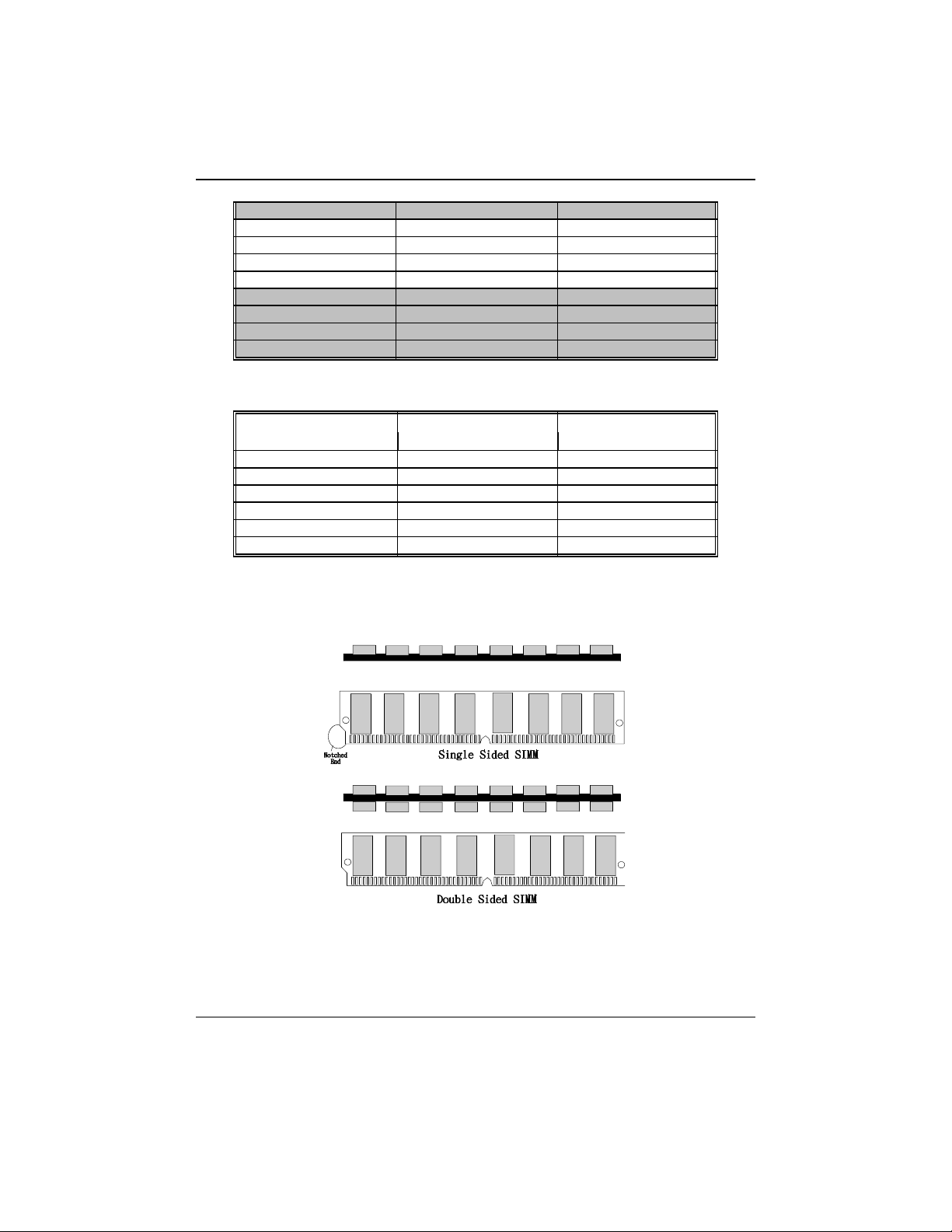
Chapter 1 System Board
80M 32M x 2 pcs 8M x 2 pcs
40M 4M x 2 pcs 16M x 2 pcs
48M 8M x 2 pcs 16M x 2 pcs
64M 16M x 2 pcs 16M x 2 pcs
96M 32M x 2 pcs 16M x 2 pcs
72M 4M x 2 pcs 32M x 2 pcs
80M 8M x 2 pcs 32M x 2 pcs
96M 16M x 2 pcs 32M x 2 pcs
128M 32M x 2 pcs 32M x 2 pcs
(a-2) SIMM1 or SIMM2 Single module (32bits) Boot.
Total SIMM1 SIMM2
Memory Size (MB)
8M 8 M x 1 pcs ----------
8M ---------- 8 M x 1 pcs
16M 16M x 1 pcs ---------16M ---------- 16M x 1 pcs
32M 32M x 1 pcs ---------32M ---------- 32M x 1 pcs
How to install a SIMM Module
1-19
Page 20
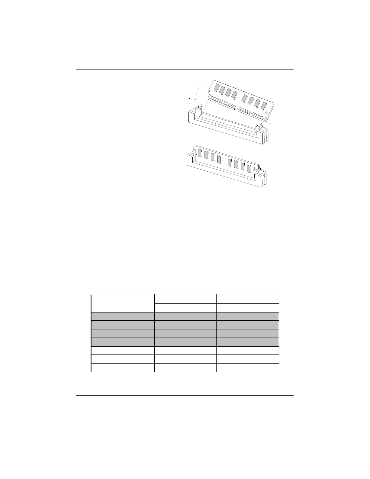
Chapter 1 System Board
1. The SIMM slot has an “ Iron
Safety Tab” and the SIMM memory
module has a “Notched End”, so the
SIMM memory module can only fit in
one direction.
2. Insert the SIMM memory modules into the socket at 45-degree angle, then push
into a vertical position so that it snaps into place.
3. The Mounting Holes and Metal Clips should fit over the edges and hold the
SIMM memory modules in place.
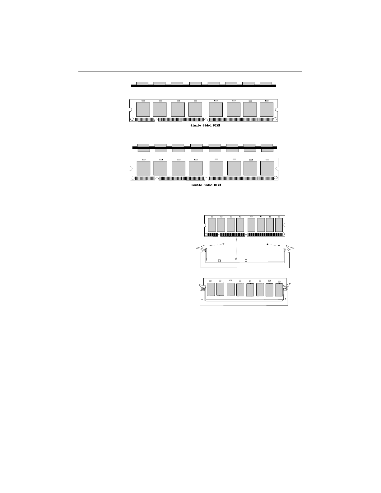
(b) DIMM (optional)
DRAM Access Time : 3.3V Unbuffered SDRAM 15ns required.
DRAM Type : 8MB/16MB/32MB/64MB DIMM Module (168pin)
Total Bank 0 Bank 1
Memory Size (MB) DIMM 1 DIMM 2
8M 8M x 1 pc ----
16M 16M x 1 pc ----
32M 32M x 1 pc ----
64M 64M x 1 pc ----
16M 8M x 1 pc 8M x 1 pc
24M 16M x 1 pc 8M x 1 pc
40M 32M x 1 pc 8M x 1 pc
1-20
Page 21

Chapter 1 System Board
72M 64M x 1 pc 8M x 1 pc
24M 8M x 1 pc 16M x 1 pc
32M 16M x 1 pc 16M x 1 pc
48M 32M x 1 pc 16M x 1 pc
80M 64M x 1 pc 16M x 1 pc
40M 8M x 1 pc 32M x 1 pc
48M 16M x 1 pc 32M x 1 pc
64M 32M x 1 pc 32M x 1 pc
96M 64M x 1 pc 32M x 1 pc
72M 8M x 1 pc 64M x 1 pc
80M 16M x 1 pc 64M x 1 pc
96M 32M x 1 pc 64M x 1 pc
128M 64M x 1 pc 64M x 1 pc
*Each Bank can be installed and used individually. The mainboard provides
optimal performance and free choices depending on your needs.
*The list show above for DRAM configuration is just for reference.
*SDRAM mixed with FP or EDO is not recommended.
How to install a DIMM Module
1-21
Page 22
Chapter 1 System Board
1. The DIMM slot has a “ Plastic Safety Tab” and the DIMM memory module has a
“an asymmetrical notch”, so the DIMM
memory module can only fit in one
direction.
2. Push the tabs out. Insert the DIMM memory modules into the socket at 90-degree
angle, then push down a vertical position so that it will snap into place.
3. The Mounting Holes and plastic tabs should fit over the edge and hold the DIMM
memory modules in place.
1-22
 Loading...