Biostar K8NHA Grand Owner's Manual

KK88 NNHHAA GGrraanndd
FCC Inf or m at ion and Copyright
Thi s equ ipm ent h a s been t es te d a nd fo un d to c om pl y w i th th e lim it s of a Cla s s
B d ig it al d e vi ce, pu r su ant to Par t 15 of th e FC C R ul e s. The se lim it s ar e
designed to pro vide reasonab le pr otection against harmful inter ference in a
residential installation. This equipment generates, use s and can radiate radio
frequency energy and, if not installed and used in accordanc e with the
in structions, may cau se harmful in terference to radio communications. There
is no guarantee th at int erferen ce will not occur in a particular in stallation.
The vendor makes no representations or warranties with respec t to the
con tent s here and spe cially disclaims any imp lied warranties of
mercha ntabilit y or fitness for any purp ose. F urther the vendor reserve s the
right to revis e this publication and to make changes to the contents here
w ithout obligation to notify any party bef oreha nd.
Duplication of this publication, in part or in whole, is not allowed without first
obt aining t he ven dor’s approv al in w r iting.
The content of this user’s manual is subject to be changed without notice and
w e will n ot b e re spo n si bl e for an y mi s tak e s fou n d in thi s us er’s man u al. All th e
brand an d produ ct names are trad emarks of their respective compani es.
i

TTaabbllee ooff CCoonntteennttss
Chapter 1: Introduction ...........................................................1
1.1 K8NHA GRAND Features.............................................1
1.2 Package Checklist........................................................4
1.3 Layout of K8 NHA GRAND.............................................5
1.3 Components of K8NHA GRAND.................................... 6
Chapter 2: Hardware Installation ..........................................7
2.1 Central Processing Unit (CPU)......................................7
2.2 Fan Headers................................................................9
2.3 Memory Mo dules Ins ta llat ion.........................................9
2.4 Conne ctors, & Slots....................................................10
Chapter 3: Headers & Jumpers Setup...............................11
3.1 How to setup Jumpers................................................ 11
3.2 Detail Settings............................................................11
Pin ............................................................................................... 11
Chapter 4: Useful Help...........................................................16
4.1 Award BIOS Beep Code.............................................16
4.2 T roubleshooting..........................................................1 6
Chapter 5: NVIDIA RAID Function ......................................18
5.1 Operat ion System.......................................................18
5.2 Raid Arrays................................................................18
5.3 How RAID Works.......................................................1 9
Chapter 6: WarpSpeeder™...................................................23
6.1 Introduction................................................................23
6.2 System Requirement ..................................................23
6.3 Installation .................................................................24
ii
KK88NNHHAA GGrraanndd
CHAPTER 1: INTRODUCTION
1.1 K8NHA GRAND FEATURES
A. Hardware
CPU
Supports Socket 754.
Supports the AMD Athl on 64 Socket 754 processor
Supports AM D Sempron Socket 754 processor
Chi pset
NVIDIA NF3 250Gb.
- Hyp er Tran sport link to t he AMD Athlon 64 CPU.
- Sup por ts AGP 3.0 8x in t er face.
- Supports sy stem and power management.
- Supports 4 IDE disk dri ves, integrated RAID 0, RAID 1 and
RAID 0 +1 functions.
- Supports PIO Mode 5, Bride Mode and Ultra DMA
33/ 66/10 0/ 1 33 Bus Mas ter Mod e.
- Supports USB 2.0, 8 ports.
- Complaints with PCI Version 2.3 specifi cati on.
- Complaints with AC’97 Version 2.3 specificati on.
- Fast ATA/133 IDE controllers.
Dimensions
ATX Form Factor: 21.5x29.3cm (W x L)
Ma in Memory
Supp orts up to 2 DDR d evi ces.
Supp orts 200/266/333/ 40 0 MHz DDR de v ices.
Certified DDR400 + List
- Please check the website:
http://www.biostar.com.tw/products/mainboard/board.php3
?name=K8NHA%20Grand
Maximum memory siz e is 2GB.
DI MM Socket
Location
DIMM1 128MB/256MB/512MB/1GB *1
DIMM2 128MB/256MB/512MB/1GB *1
DDR Module
To t al M e m o r y
Size (MB)
Max is 2 GB.
Slots
5 x 3 2-bi t PCI bus m aster sl ots.
1 x AGP 8x slot
1
KK88NNHHAA GGrraanndd
Super I/O
Chip: ITE IT8712F.
Low Pin Count Interface.
Provides the most commonly used legacy Super I/O
functionality.
Environment Control initiatives,
- H/W Monitor
- Fan Speed Controller
- IT E's " S mart Guardi an" fu n ction
On Board IDE
Supports 4 IDE disk dri ves.
Supports PIO mode 4, Block M ode and Ultra DMA
33/ 66/10 0/ 1 33 bus mas t er mo de.
10/100 LA N (optional)
PHY: RTL8201BLC
Supports 10 Mb/s and 100 Mb/s auto-negotiation.
Half/ Full duplex capabil ity.
Gigabit LAN
NVIDIA Gigabit MAC + VITESSE Gigab it PHY VSC8201
(CIS8201).
Supports 10 Mb/s, 100 Mb/s and 1Gb/s auto-negotiation.
Half/ Full duplex capabil ity.
Supports personal Firewall setup.
Suppor ts ACPI power m anagement.
Supports NVIDIA StreamT h ru te chnology
- Isochronous controll er pai red with Hyper T ransport resul ts
in fas t es t networ king perf ormance
Se cu rity
NVIDIA Firewall technology
- Native fire wall solution
Advanced features
- Remote access, configuration, monitoring
- Com man d l in e int er f ace (C LI)
- WMI scripts.
Se rial ATA
Supports 2 serial ATA (SATA) ports.
Compli ant with SATA 1.0 specification.
Data transfer ra te s up to 1 50 M B/s
2

KK88NNHHAA GGrraanndd
Storage
NVIDIA RAID Technology
- RAID 0 disk stri ping for highest system and application
performance
- RAID 1 disk mirroring support for fault tolerance
Support for both SATA and ATA-133 disk controller
standards
- RAID 0+1 disk stri pi ng and mirroring for highest
performance with fault tolerance
IEEE 1394A Chi p
Chip: VIA VT6307.
Support 2 ports with transfer up to 400Mb /s.
On Board A C’97 Sound Cod ec
Chip: ALC655
Compli ant with AC’97 Version 2.3 specification.
Supports S/PDIF Out (optional function).
Supports 6 channels.
F ront Sid e On-bo ard P er iphera ls
1 seri al header supports 1 serial COM port. (JCOM 2, optional)
1 audio out header supports 1 line-in, 1 line-out, and 1MIC
ports.
1 CD-i n connector supports 1 CD-ROM devi ce.
1 S/P DIF out connector supp o rts 1 S/PDIF ou t port (op tion al).
1 IEEE1394 header supports 1 IEEE 1394 port.
1 floppy connector supports 2 FDD devices with 360K, 720K,
1.2 M, 1.44M and 2.88M by tes.
2 USB headers support 4 USB 2.0 ports.
2 IDE connectors support 4 hard disk devices.
2 Seri al ATA connectors support 2 SATA devices.
3

KK88NNHHAA GGrraanndd
Re ar (Back) S id e Co n n ect or s
1 par allel por t.
1RJ-45 LAN jack.
1 IEEE1394 port (optional).
1 audio port.
1 PS/2 keyboard & m ouse port.
2 seri al ports (JCOM3 is optional).
4 USB 2.0 ports.
PS/2
Mouse
PS/2
Keyboard
1394
(optional)
USB x2
COM1
Parallel
COM3
(optional)
B. BIOS & Software
BIOS
Award legal BIOS.
Sup por ts APM1. 2 , AC PI , an d USB fu nctio ns.
Software
Sup por ts W ar pspee der ™ , 9th T o uch™ , W IN FLA SH ER ™ an d
FLASHER™.
Offers the highest performance for Windows 98 SE, Windows
2000, Windows Me, Windows XP, SCO UNIX etc.
1.2 PACKAGE CHECKLIST
FDD Cable X 1
HDD Cable X 1
User’s M anual X 1
Fu lly Setu p Driver CD X 1
Rear I/O Panel fo r ATX Case X 1
USB 2.0 Cable X1 (opti onal)
S/PDIF Cable X 1 (optional)
Serial ATA Cable X 1 (opti onal)
IEEE 1394 Cable X 1 (optiona l)
Serial ATA Power Switch Cable X 1 (optional)
LAN
USB x2
Line In/
Surround
Line Out
Mi c I n 1 /
Bas e/Cente r
4
KK88NNHHAA GGrraanndd
A
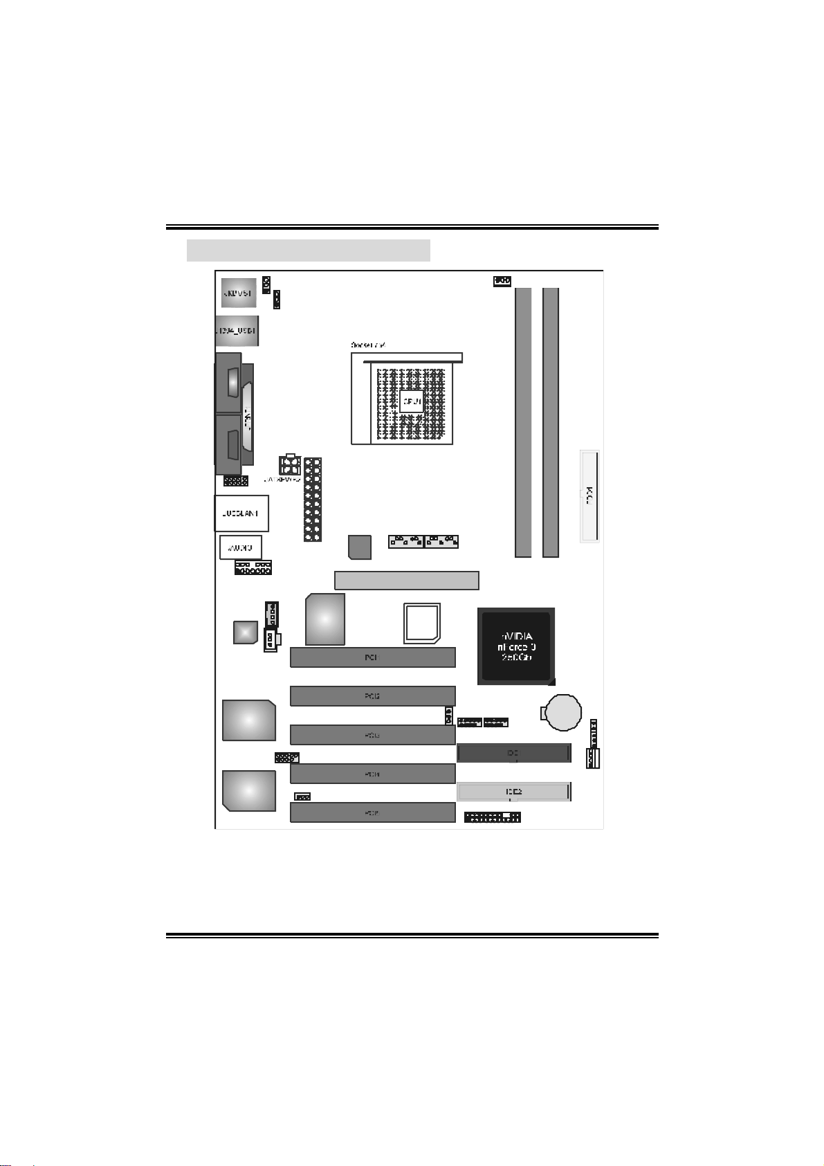
1.3 LAYOUT OF K8NHA GRAND
1
JCOM2*
1
JC OM3* JCOM1
1 JAUDI O1
Codec
JSPDIF _OUT
JKBMSV1
1
1
JUSBV1
JCDIN1
1
JATX PWR 1
IT8712F
RTL
8201BL
JSATA517JSATA4
17
GP1
BIOS
1
JCFAN1
DDR1
DDR2
VSC8201
VT6307
J1 39 4A1
1
J1 394 V1
1
1
JUSB2
1
JPANEL1
2
1
JUSB1
1
BAT1
JCI1
JCMOS1
JSFAN1
24
23
JUSBV3
Note:
1. ● represents the 1st pin.
2. *: JCOM2 and JCOM3 are optional, and only one of them can be
chosen.
5
1
1
1

KK88NNHHAA GGrraanndd
A
A
OPQ
R
1.3 COMPONENTS OF K8NHA GRAND
B
C
V
D
E
F
G
H
I
J
K L
JATXPW R 1~2: ATX power
A.
Codec
VSC8201
VT6307
connectors.
JU SBV1: Power sourc e f or
B.
J1394_USB1.
JKBMSV1: Power source f or
C.
JKBMS1.
Back panel connectors.
D.
JAU DIO1: Audio out header.
E.
AGP1: Accelerated Graphic s Port
F
slot.
JCDIN1: CD-ROM audio-in header
G.
JSPD IF_OU T: Digit al audio out
H.
header (optional).
PCI 1~5: Peripheral Com ponent
I.
Int erc onnect slots.
J1394A1: Front 1394 header.
J.
J1394V1: Power source for
K.
J1394A1.
IT8712F
82 01 B L
DDR1
DD R2
RT L
GP1
BIOS
BAT1
U
T
S
N
M
JPANEL1: Front panel c onnector.
L.
ID E1~2: Hard disk connectors.
M.
JSFAN1: Syste m fan connector.
N.
JCMOS1: Clear CMOS Heade r.
O.
JCI1 : Case open Header.
P.
JU SB1~2: Front USB headers .
Q.
JU SBV3: Power sourc e f or JUSB1~2.
R.
JSATA4~5: Serial ATA c onnec t ors.
S.
FDD1: Flopp y disk connector.
T.
DDR1~2: DDR memor y modules.
U.
JCFAN1: CPU fan conne cto r.
V.
6

KK88NNHHAA GGrraanndd
CHAPTER 2: HARDWARE INSTALLATION
2.1 CENTRAL PROCESSING UNIT (CPU)
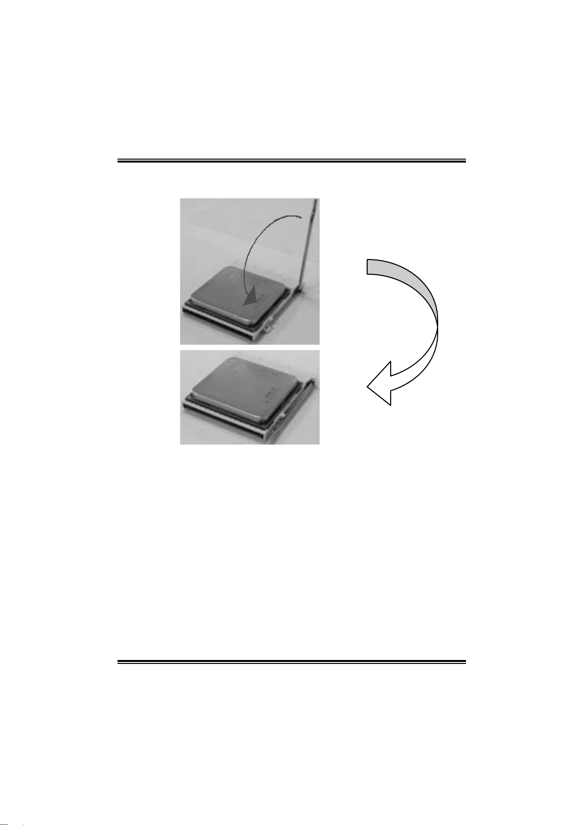
Step 1: Pull the lever sideways away from the socket and then raise the
lever up to a 90-degree angle.
Step 2: Look for the black cut edge on socket, and the white dot on CPU
should point forwards this bl ack cut edge. The CPU will fit only in
the correct orientation.
7
KK88NNHHAA GGrraanndd
Step 3: Hold the CPU down firml y, and then close the l ever to complete
the i nstal la ti on.
Step 4: Put the CPU F an on the CPU and bu c kl e it. Conn ec t the CPU
FAN power cable to the JCFAN1. This completes the installation.
8

KK88NNHHAA GGrraanndd
2.2 FAN HEADERS
CPU FAN Header: JCFAN1
Pin Assignment
1
JCFAN1
1 Ground
2 +12V
3 FAN RPM rat e s ens e
System Fan Header: JSFAN1
1
JSFAN1
Note:
The JCF AN1 and J SF AN 1support sy stem cooling fan wit h Sm art Fan Cont rol
utility. It support s 3 pin head c onnector. When connect ing wit h wires onto
connec t ors, please not e t hat t he red wire is the pos itive and should be
connec t ed to pin#2, and the black wire is Ground and should be connected to
GND.
Pin Assignment
1 Ground
2 +12V
3 FAN RPM rat e s ens e
2.3 MEMORY MODULES INSTALLAT ION
2.2.1 DDR M o dule ins tallation
1. Unlock a DIMM sl ot by pressi ng the retaining cli ps outward. Align a
DIMM on the slo t su ch that the notch on the DIMM ma tches the b reak
on the Sl ot.
2. Insert the DIMM vertically and firmly into the slot until the retaining
chip snap back in place and the DIM M is properly seated.
9

KK88NNHHAA GGrraanndd
2.4 CONNECTO RS, & SLOTS
Floppy D isk Connector: FDD1
The motherboard provi des a standard floppy di sk connector that
s uppor t s 360 K, 720K, 1. 2 M, 1.4 4M a nd 2.8 8 M flo ppy d isk types. This
connector supports the provi ded floppy drive ribbon cabl es.
Hard Disk Connectors: IDE1~ 2
The motherboard has a 32-bit Enhanced PCI IDE Controller that
provides PIO Mode 0~5, Bus M aster, and Ul tra DMA 33/66/100/133
functio nality. It ha s two HDD c onnectors IDE1 (primary ) an d IDE2
(secondary).
The IDE connectors can connect a master and a slave drive, so you
can connect up to four hard disk dri ves. The fi rst hard drive should
al ways be conne cted to IDE1.
Peripheral Component Interconnect Slots: PCI1~5
This motherboard i s equipped with 1 standard PCI slot. PCI stands for
Peripheral Component Interconnect, and i t is a bus standard for
expansion cards. T his PCI slot is designated as 32 bits.
Serial ATA Connectors: JSATA4~5
The motherboard has a SATA Controller in nForce 3 250Gb with 2
channels SATA interface, it satisfies the SATA 1.0 spec and wi th
tr ansfer rate of 1.5 Gb/ s.
Pin Assignment Pin Assignment
7
JSATA4/JSATA5
1
1 Ground 2 TX+
3 TX- 4 Ground
5 RX- 6 RX+
7 Ground
10
KK88NNHHAA GGrraanndd
CHAPTER 3: HEADERS & JUMPERS SETUP
3.1 HOW TO S ETUP JUMP ERS
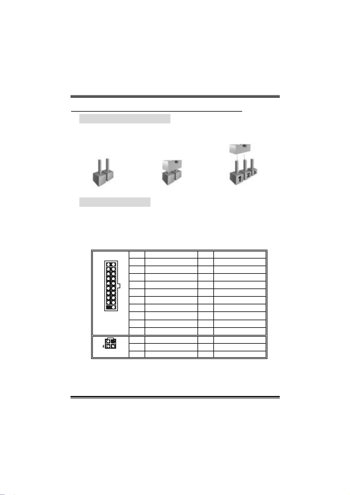
The il lustration shows how to set up jumpers. When the jumper cap is
placed on pins, the jumper is “close”, if not, that means the jumper i s
“open”.
Pin opened Pin closed Pin1-2 closed
3.2 DETAIL SETTINGS
Pow er Conn ector s: JATX PWR1/PAT X PWR2
JATXPWR1: Thi s connector allows user to connect 20-pin power
conn ec tor on t h e A TX power s upply.
JATXPWR2: By connecting this connector, it will pro vi de +12V to CPU
power circui t.
Pin Assignment Pin Assignment
10
1
JATXPWR1
12
3
JATXPWR2
1 +3.3V 11 +3.3V
20
2 +3.3V 12 -12V
3 Ground 13 Ground
4 +5V 14 PS_ON
5 Ground 15 Ground
6 +5V 16 Ground
7 Ground 17 Ground
11
8 PW_OK 18 -5V
9 Standby Voltage +5V 19 +5V
10 +12V 20 +5V
Pin Assignment Pin Assignment
1 +12V 3 Ground
2 +12v 4 Ground
11
KK88NNHHAA GGrraanndd
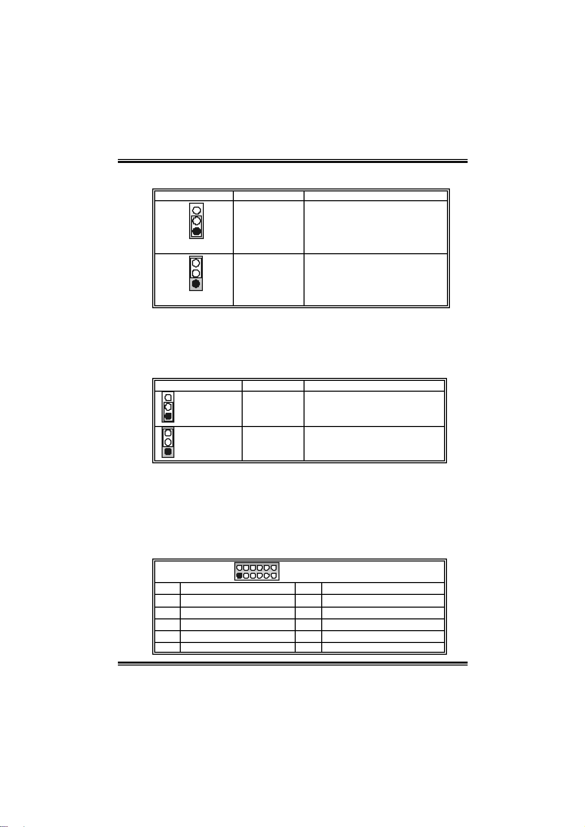
Powe r Sou rce Selection He aders for USB: JUSBV1/JUSBV3
JUSBV1/JUSBV3 Assignment Description
3
1
Pin 1-2 clo se
Pin 2-3 clo se
3
1
+5V
+5V st andby
Voltage
Note:
In order to support this function “Power-on system via USB device,”
“JUSBV1/JUSBV3” jumper cap should be pl ace d on Pi n 2-3
individually.
JUSBV1: +5V for USB at the
J1394_U SB1 and JU SBLAN 1
connec t or ports.
JUSBV3: +5V for USB at the JUSB
1~2 connector port s.
JU SBV1: J1394_USB1 and
JU SBLAN 1 ports powered with
st andby v olt age of +5V
JU SBV3: JUSB1~2 ports powered
with standby v olt age of 55V
Power S o urce Se lec tio n H ead er s for K eyb o ar d /Mo us e: JKBM SV1
JKBMSV1 Assignment Description
3
1
Pin 1-2 close
3
1
Pin 2-3 close
Note:
In order to support this function “Power-on system via keyboard and
mouse”, “JKBM SV1” jumper cap shoul d be placed on Pin 2-3.
+5V +5V for ke yboard and mouse
+5V Standby
Voltage
PS/2 m ouse and PS/ 2 k eyboard
are powered wit h +5V s t andby
voltage.
COM2 Header: JCOM2 (Optional)
This header allows user to connect additional seri al cable on the PC
back panel. It can be used to connect serial devi ces, for example,
mouse or modem.
2
1
Pin Assignment Pin Assignment
1 RIN1 2 RIN3
3 DOUT2 4 DOUT3
5 Ground 6 RIN2
7 DOUT1 8 RIN4
9 -XRI1 10 NA
10
9
JCOM2-Header
12
KK88NNHHAA GGrraanndd
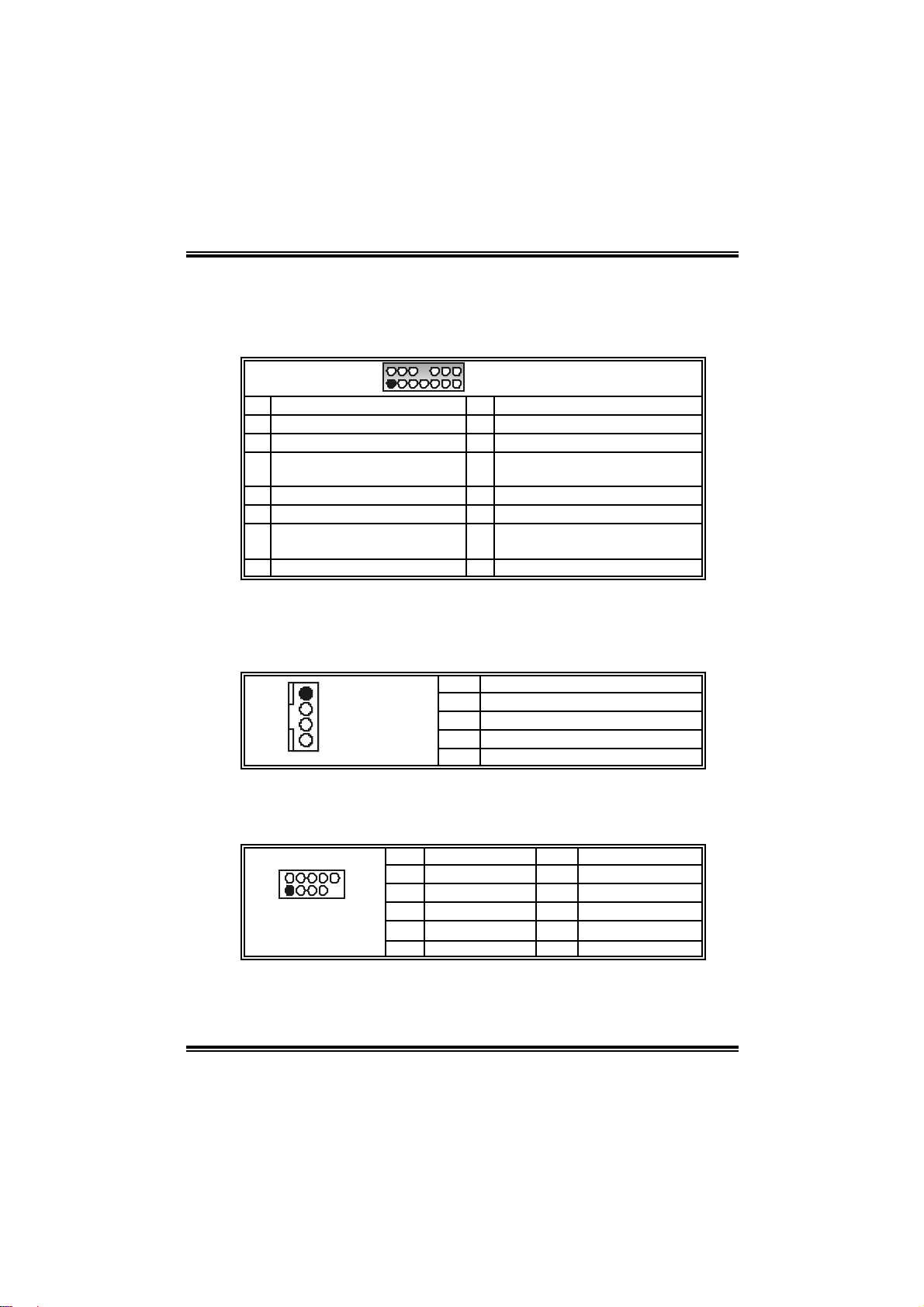
Front Panel Audio Out Header: JAUDIO1
This conn ec to r will allow user to c on nect with t he front audio out pu t
headers on the P C c ase. It will disable the ou tp ut on b ac k pan el audio
connectors.
2
1
Pin Assignment Pin Assignment
1 Mic in/center 2 Ground
3 Mic power/Bas s 4 Audio power
Right line out/ Speak er out
5
Right
7 Reserved 8 Key
9 Left line out /Speaker out Left 10 Lef t line out/Speaker out Left
Right line in/R ear s peak er
11
Right
13 Lef t line in/ R ear speak er Lef t 14 Left line in/R ear speak er Lef t
14
13
JAUDIO1
6 R ight line out/ Speak er out R ight
12 Right line in/Rear speaker Right
CD-ROM Audio -in Conne c tor: JCDIN1
This connector all ows user to connect the audio source from the veriaty
devices, like CD-ROM, DVD-ROM, PCI sound card, PCI TV turner card
etc..
1
JCDIN1
Pin Assignment
1 Left channel input
2 Ground
3 Ground
4 Right channel input
F r ont 13 94 He ader: J1 394A 1
This connector all ows user to connect the front 1394 port for digital
image devices.
Pin Assignment Pin Assignment
2
1
J1394A1
10
9
1 A+ 2 A3 Ground 4 Ground
5 B+ 6 B7 +12v 8 +12V
9 Key 10 Ground
13

KK88NNHHAA GGrraanndd
Digi ta l Aud io Out Co nn ector: JS PDI F _ OUT (opt ion al)
This conn ec to r will allow user to c on nect the PCI brac ket SPDI F output
header.
Pin Assignment
1 +5V
1
JSPDIF_OUT
2 SPDIF OUT
3 Ground
Power Source for 1394: J1394V1
J1394V1 Assignment Description
1 3
Pin 1-2 clo se
1
Pin 2-3 clo se
+3.3V SB +3.3V SB f or 1394 c hipset.
3
+3.3V
+3.3V for 1394 chipse t.
(Default)
F r ont Pa n el Con n ect or: JPA NEL1
This 24-pin c on nector in cl ud es Power-on, Reset , HDD L ED, Po wer
LED, Sleep button, speaker and IrDA Connection. It allows user to
connect the PC case’s front panel switch functions.
2
1
Pin Assignment Function Pin Assignment Function
1 +5V 2 Sleep control
3 N/A 4 Ground
5 N/A 6 N/A N/A
7 Speaker
9 H DD LED (+) 10 Power LED (+)
11 HEE LED (-)
13 Ground 14 Power button
15 Reset control
17 N/A 18 Key
19 N/A 20 Key
21 +5V 22 Ground
23 IRTX
Speaker
Connector
Hard driv e
LED
Res et button
IrDA
Connector
8 Power LED (+)
12 Power LED (-)
16 Ground
24 IRRX
24
23
JPANEL1
Sleep butt on
Power LED
Power-on button
IrD A Connec t or
14
KK88NNHHAA GGrraanndd
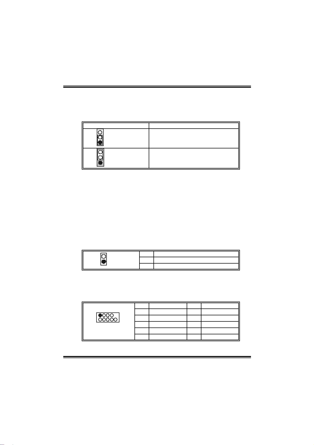
Clear CM OS Head er: J CM OS1
By placing the jumper on pin2-3, it all ows user to restore the BIOS safe
setting and the CMOS data, pl ease carefully follow the procedures to
avo id da ma ging th e mot her boar d.
JCMOS1 Assignment
3
1
Pin 1-2 close
3
1
Pin 2-3 close
Norm al Operation (D ef ault ).
Clear CMOS data.
※ Clear CMOS Procedures:
1. Remove AC power line.
2. Set the jumper to “Pin 2-3 close”.
3. Wai t for fi ve seconds.
4. Set the jumper to “Pin 1-2 close”.
5. Power on the AC.
6. Reset your desired password or clear the CMOS data.
Case Op en Head er : JCI 1
T his connector allows system to monitor PC case op en status. If the
signal has been triggered, it wil l record to the CMOS and show the
message on next boot-up.
Pin Assignment
1
JCI1
1 Cas e open signal
2 Ground
Front USB Header: JUSB1~2
This connector all ows user to connect additional USB cables on the PC
front panel. Also can be connected with internal USB devices, like USB
card reader.
1
2
JUSB1/JUSB2
10
Pin Assignment Pin Assignment
1 +5V (fused) 2 +5V (fused)
3 USB- 4 USB5 USB+ 6 USB+
7 Ground 8 Ground
9 Key 10 NC
15
KK88NNHHAA GGrraanndd
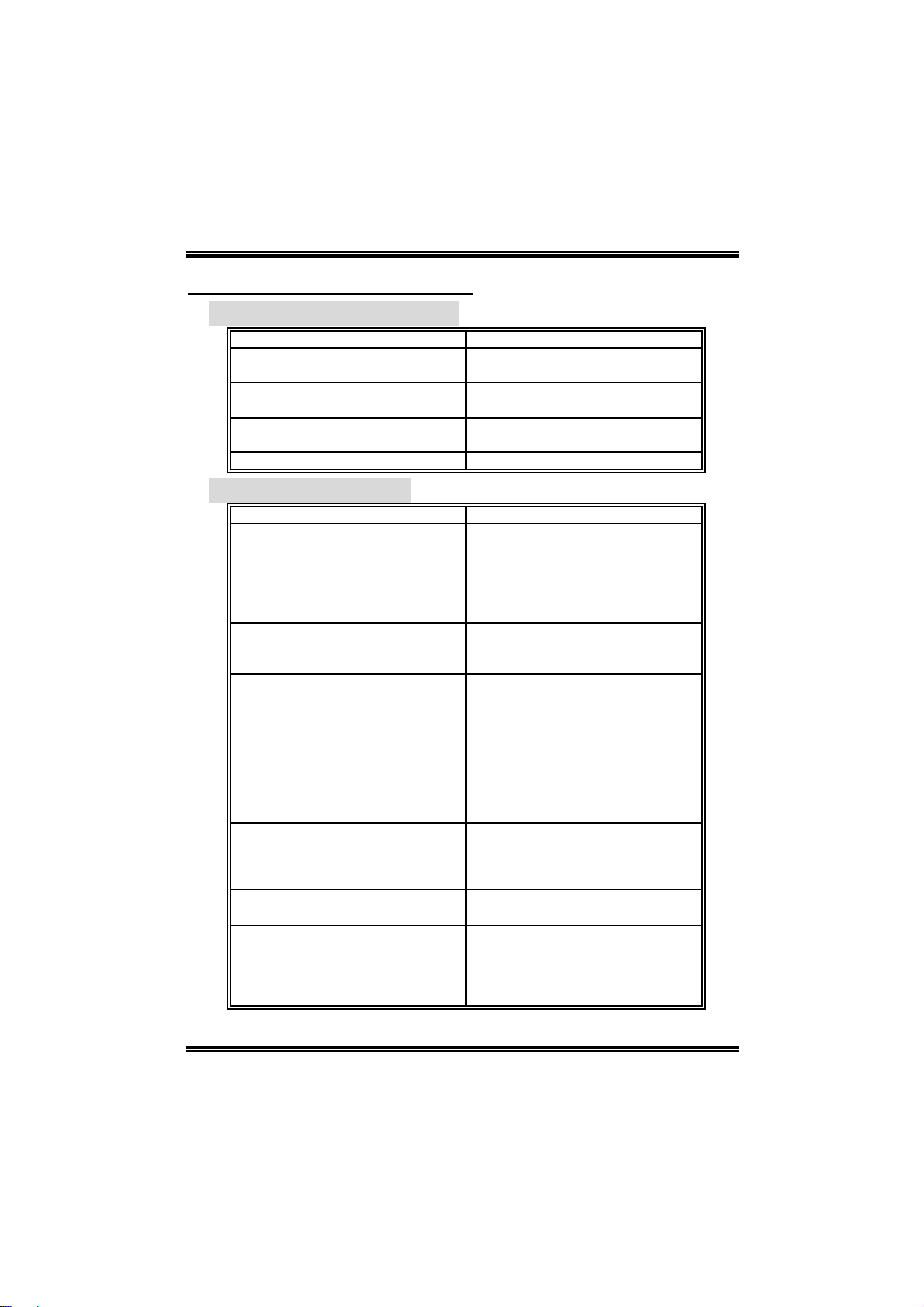
CHAPTER 4: USEFUL HELP
4.1 AWAR D BIOS BEEP CODE
Beep Sound Meanin g
One long beep f ollowed by t wo s hort
beeps
High-low siren sound C PU ov erheat ed
One Short beep when system
boot-up
Long beeps every ot her s econd No DRAM detected or inst all
4.2 TROUBL ESHOOTIN G
Probable Solution
1. N o power to the system at all
Power light don’t illuminat e, fan
inside power supply does not
turn on.
2. I ndic at or light on k ey board does
not t urn on.
Sys t em inoperat iv e. Key board lights
are on, power indic at or lights are lit,
and hard drive is s pinning.
Sys t em does not boot f rom hard disk
drive, can be boot ed f rom opt ic al
drive.
Sys t em only boot s from opt ic al driv e.
Hard disk can be read and
applicat ions can be used but booting
from hard disk is impossible.
Screen m essage say s “Inv alid
Conf igurat ion” or “CMOS Failure. ”
Cannot boot sys t em after inst alling
sec ond hard drive.
Video card not f ound or v ideo card
mem ory bad
Sys t em will shut down aut omatically
No error found during POST
1. Make s ure power c able is
sec urely plugged in.
2. Replace cable.
3. Contact technical support.
Us ing even pres s ure on both ends of
the DIMM, press down firm ly until t he
module s naps int o plac e.
1. C hec k cable running from disk to
disk controller board. Make s ure
both ends are s ec urely plugged
i n; check t h e dr iv e ty pe in the
standard CMOS setup.
2. Bac k ing up the hard driv e is
ext rem ely im port ant . All hard
disk s are c apable of breaking
down at any t im e.
Back up data and applic at ions f iles.
Ref orm at t he hard driv e. R e-install
applicat ions and dat a us ing backup
disks.
Rev iew system’s equipm ent. Make
sure c orrect information is in setup.
Set master/slave jumpers correctly.
Run SETUP program and s elec t
correc t drive ty pes. C all the driv e
manuf acturers for com pat ibility with
other driv es.
16

KK88NNHHAA GGrraanndd
17
 Loading...