

Page 1

C h a p t e r 1
System Introduction
System Introduction 1-1
1.1 Overview
1.1.1 System Board
The M9B is a dual-processor system board that supports the Intel Pentium Pro CPU. It contains
an exclusive slot for the Pentium Pro CPU board that carries two zero-insertion force (ZIF) CPU
sockets.
This high-performance 64-bit system board utilizes both the EISA and the PCI local bus
architecture. Two EISA, four PCI bus slots, and one EISA/PCI shared slot reside on the board to
allow installation of either master or slave devices.
The system board has four DRAM banks composed of eight 72-pin SIMM sockets that
accommodate both fast-page mode and EDO (extended data output) SIMMs. The sockets support
a total of 256-MB system memory using 32-MB SIMMs.
A 50-pin Fast SCSI-II interface and a 68-pin Wide SCSI interface come with the system board to
connect SCSI devices. Standard external I/O interfaces include two 9-pin serial ports, one parallel
port, a video port, and keyboard and mouse ports.
The system board supports two optional features, the ASM Pro and the remote diagnostic
management (RDM), that allow better server management. The ASM Pro detects problems in
CPU thermal condition, 5V/3.3V/1.5V detection, and PCI bus utilization calculation. The RDM
allows execution of the RDM diagnostic program from a remote RDM station to fix detected
problems or to reboot the system.
1.1.2 CPU Board
The Pentium Pro CPU board carries two ZIF sockets (Socket 8) to accommodate the new Pentium
Pro CPUs running at 180 MHz and 200 MHz.
The board also includes the PCI bridge/memory controller (PMC) and the data bus
accelerator (DBX) chipsets. The PMC provides bus control signals and address paths for transfers
between the host bus, PCI bus, and the main memory. The DBX supoorts multiple-bit error
detection and sigle-bit error correction through the ECC/parity feature.
Page 2

1-2 Service Guide
1.1.3 Features
The M9B system has the following features:
• A separate CPU board that carries the Pentium Pro CPU and the 512-KB synchronous
pipeline burst second-level cache
• Four PCI slots, two EISA slots, and one PCI/EISA shared slot, with all PCI slots supporting
master devices
• Four DRAM banks composed of eight 72-pin SIMM sockets that support 8/16/32-MB
70ns fast-page mode or EDO-type SIMMs
• Fast SCSI and Wide SCSI interfaces
• Standard 1-MB video DRAM onboard plus two upgrade sockets for up to 2-MB video memory
• 256-KB Flash ROM BIOS
• System clock/calendar with 8KB CMOS RAM with battery backup
• Onboard interfaces for front panel LED and backplane board SCSI HDD status indicator
• ASM Pro and remote diagnostic management (RDM) features
• Power management features (IDE hard disk standby mode and system suspend mode)
• External ports:
• PS/2 keyboard and mouse ports
• Two buffered high-speed serial ports (NS16C550-compatible UARTs with 16-byte FIFOs)
• One ECP/EPP high-speed parallel port (IEEE 1284-compliant)
• Video port
• Onboard controller chipsets
• Cache/memory/buffer controller (82439HX)
• EISA System Component (ESC 82374SB)
• PCI-EISA Bridge (PCEB 82375SB)
• SCSI controller (AIC 7880)
• PCI-to-PCI Bridge (DEC 21052)
• Super I/O controller (SMC 37C665)
• PCI local bus VGA with enhanced GUI acceleration (ATI 264CT)
Page 3

System Introduction 1-3
1.2 Board Layouts
1.2.1 System Board
1 COM1
2 COM2
3 Mouse port
4 Keyboard port
5 Video port
6 Parallel port
7 Video RAM upgrade sockets
8 CPU board slot
9 PCI slots
10 EISA slots
11 Real-time clock
12 Flash ROM BIOS
13 Buzzer
14 Narrow SCSI connector
15 Wide SCSI connector
16 SIMM sockets
17 Fan connector 1 (FA1)
18 Fan connector 2 (FA2)
19 Fan connector 3 (FA3)
20 Power connector
21 Power connector
22 Video RAM
23 RDM connectors
Figure 1-1 System Board Layout
3
6
1
258
91019181720212315141213111622
4
7
Page 4

1-4 Service Guide
1.2.1 CPU Board
Figure 1-2 CPU Board Layout
Fan1
CPU 2 Socket
CPU Voltage Regulators
Fan2
CPU 1 Socket
VRM Socket
VRM Socket
Page 5

System Introduction 1-5
1.3 Jumpers and Connectors
Figure 1-3 System Board Jumper and Connector Locations
Figure 1-4 CPU Board Jumper Locations
CN3 CN1 CN2
J16
Page 6
1-6 Service Guide
1.3.1 Jumper Settings
System Board
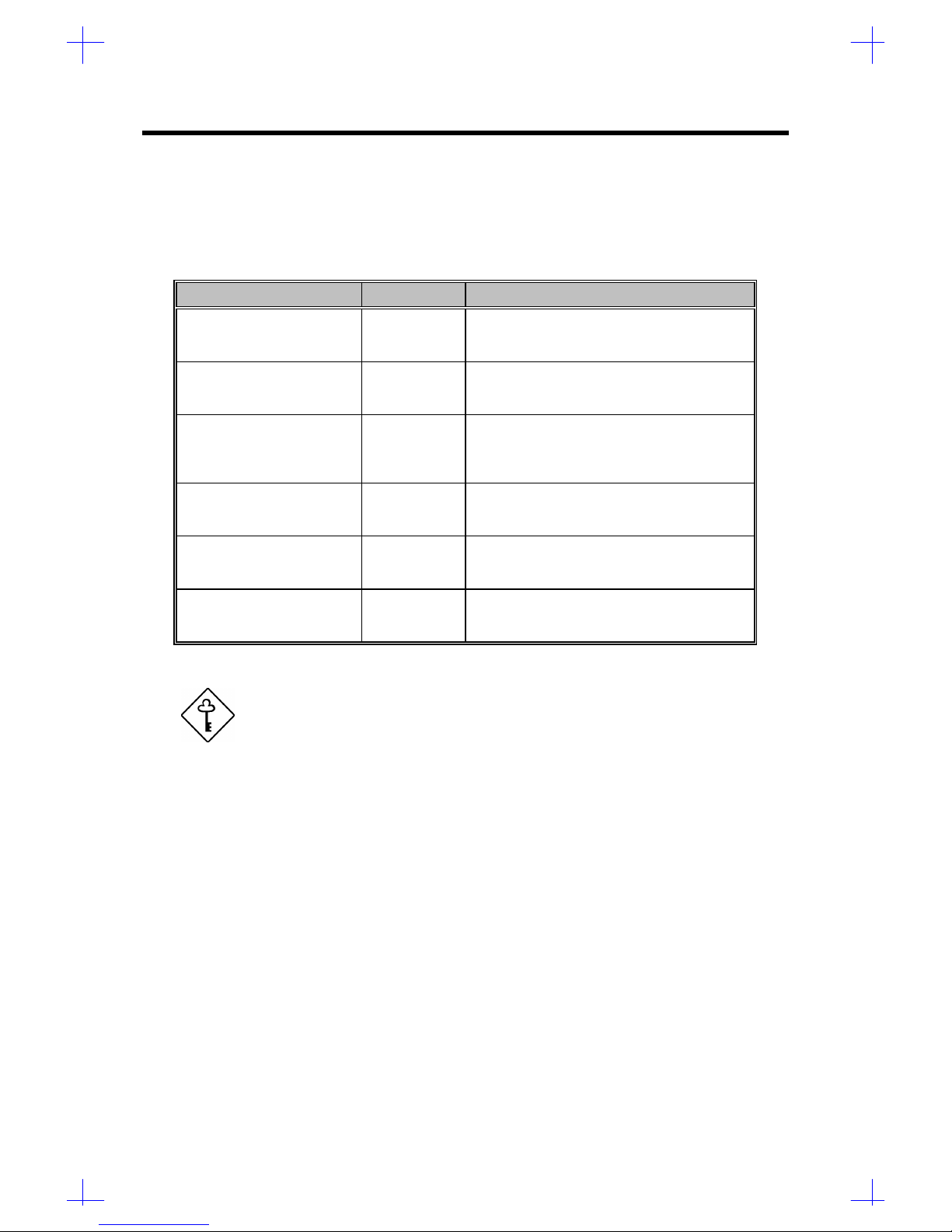
Table 1-1 System Board Jumper Settings
Jumper Setting Function
Password Security
JP1 1-2
2-3
Check password
Bypass password
BIOS Type
JP2 1-2
2-3
Acer
OEM
SCSI Termination
JP3 1-2
2-3
Terminator always set to ON
Use SCSI Setup Utility to set terminator to
ON or OFF
SCSI Feature
JP4 1-2
2-3
Wide SCSI
Standard
Hardware Reset
JP5 1-2
2-3
Enabled
Disabled
Sound Feature
JP6 1-2
2-3
Buzzer
Speaker
If both narrow and wide SCSI interfaces are present, set JP4 to
pins 1-2 for wide SCSI function.
Page 7
System Introduction 1-7
CPU Board
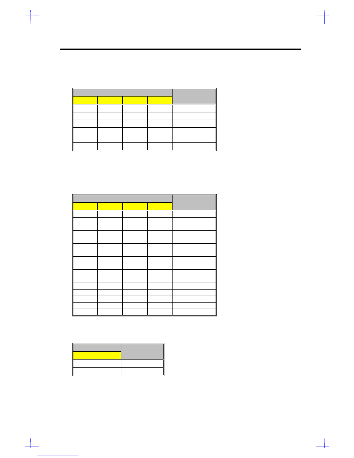
Table 1-2 CN1 Settings for CPU Core/Bus Frequency Ratio
CN1 Settings CPU Core /
1-5 2-6 3-7 4-8 Bus Freq. Ratio
1 1 1 1 2
1 1 0 1 3
1 1 1 0 4
1 1 0 0 5
0 1 1 1 2.5
0 1 0 1 3.5
0 - Pins open 1 - Pins Closed
Table 1-3 lists the CPU core voltages depending on CN2 and CN3 settings.
Table 1-3 CN2 and CN3 Settings for CPU Core Voltage
CN2/CN3 Settings
1-5 2-6 3-7 4-8 CPU Voltage
1 1 1 1 3.5
1 1 1 0 3.4
1 1 0 1 3.3
1 1 0 0 3.2
1 0 1 1 3.1
1 0 1 0 3.0
1 0 0 1 2.9
1 0 0 0 2.8
0 1 1 1 2.7
0 1 1 0 2.6
0 1 0 1 2.5
0 1 0 0 2.4
0 0 1 1 2.3
0 0 1 0 2.2
0 0 0 1 2.1
0 0 0 0 Reserved
0 - Pins open 1 - Pins Closed
Table 1-4 Clock Settings
J16 CPU
1-2 2-3 Clock Speed
1 0 60 MHz
0 1 66 MHz
0 - Pins open 1 - Pins Closed
Page 8
1-8 Service Guide
1.3.2 Connector Functions
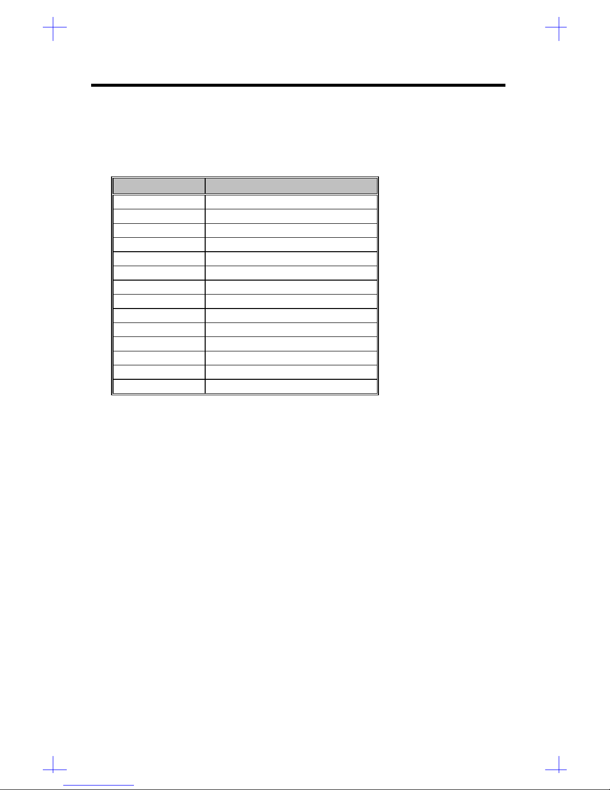
Table 1-5 lists the different connectors on the system board and their respective functions.
Table 1-5 System Board Connectors
Connector Function
CN1 Power connector
CN2 Power connector
CN3 Backplane board HDD status connector
CN5 IDE hard disk connector
CN6 RDM connector
CN7 RDM connector
CN8 Diskette drive connector
CN11 68-pin Wide SCSI connector
CN12 50-pin Fast SCSI-II connector
CN13 RDM cable and LED board connector
CN14 Hard disk LED connector
CN15 Power LED connector
CN16 Speaker connector
SW1 NMI switch
Page 9

System Introduction 1-9
1.4 System Specifications
Table 1-6 System Specifications
Item Description
CPU
P54C/P55C, 100/120/133/150/166/200 MHz
System Memory
Eight SIMM sockets that support up to 256 MB of system memory
using 60/70ns 4/8/16/32-MB SIMMs1.
Video Memory
Onboard 1-MB (256K16x2) video memory upgradable to 2-MB by
installing another two pieces of 256K16 70ns SOJ chip into the
upgrade socket
Cache
Onboard 512-KB synchronous pipeline burst second-level cache
data SRAM chip (32K32x4)
Onboard 64-KB tag SRAM chip (32K8x2)
BIOS
2
256-KB Flash ROM for system, SCSI and video BIOS
Video interface
Onboard ATI264CT PCI accelerator that supports a resolution of
1024x768, 65536 color interlaced with 2-MB video RAM.
Hard Disk Interface
IDE interface supports up to two IDE devices
PCI bus master fast SCSI II interface supports up to seven devices
or fifteen SCSI devices when wide SCSI is used.
Diskette Drive Interface
One diskette drive interface that supports 2.88/1.44/1.2-MB
diskette drives
Supports three-mode diskette type
Onboard I/O
One PS/2 keyboard port (6-pin, mini-din type x1)
One PS/2 mouse port (6-pin, mini-din type x1)
Two NS16C550-compatible serial ports (9-pin D-type x2)
One ECP/EPP parallel port (15-pin D-type x1)
Real-time Clock
System clock/calendar with 128 bytes extended CMOS RAM and
battery backup
Expansion slots
One CPU board slot
Two first-level PCI bus slot (master/slave)
Two second-level PCI bus slot (master/slave)
Two EISA bus slot (master/slave)
One first-level PCI/EISA shared bus slot (master/slave)
Power Supply
525/350/200-watt switching power supply
Housings
IDUN or IDATX housing
1
Supports both traditional fast-page mode and EDO mode SIMMs.
2
Supports PCI v2.1, PnP v1.0a, and APM v1.1 protocols.
Page 10
1-10 Service Guide
1.5 Hardware Configurations
1.5.1 Memory Configurations
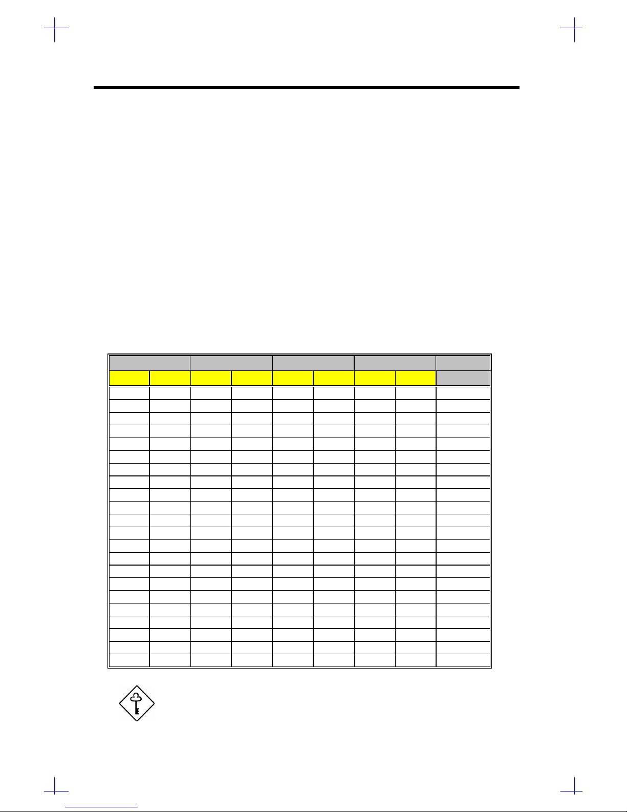
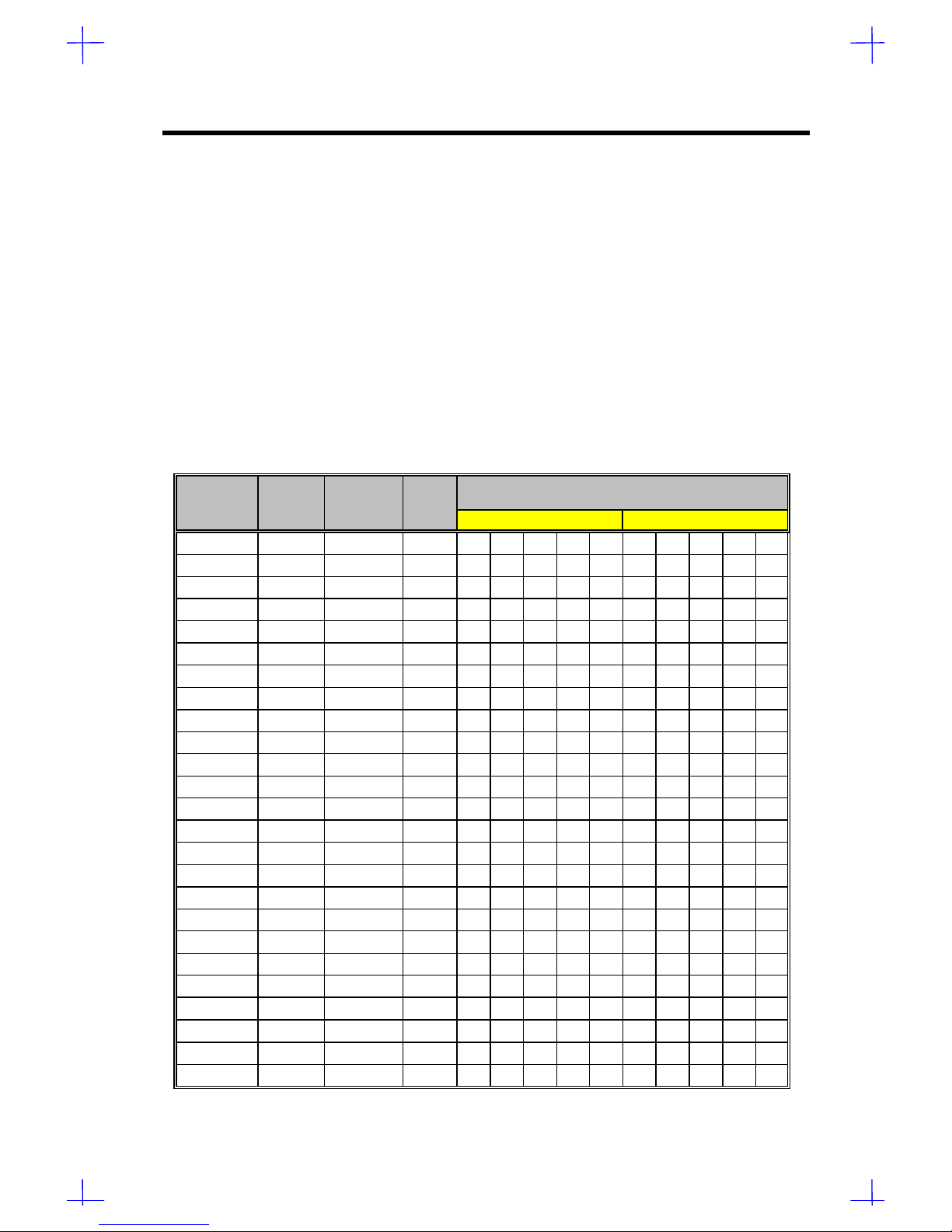
The system board comes with eight 72-pin SIMM sockets that support 4-MB and 16-MB singledensity SIMMs as well as 8-MB and 32-MB double-density SIMMs for a total system memory of
256-MB. The sockets support both the fast page mode and EDO 60/70 ns SIMMs.
Rules for Adding Memory
• You may use the memory banks (Bank0 ~Bank3) in any order.
• Use only one type of SIMM in a given bank. You may combine EDO or fast-page mode
SIMMs for a memory configuration as long as the SIMMs in each bank are of the same type.
• Use only SIMMs with the same capacity in a bank. For example, do not combine 8-MB and
16-MB SIMMs in a bank.
• Always install SIMMs in pairs. For example, for a total memory of 16 MB, install two 8-MB
SIMMs in a bank. You can not use a 16-MB SIMM alone for a 16-MB memory.
Table 1-7 Memory Configurations
Bank0 Bank1 Bank2 Bank3 Total
S1 S2 S3 S4 S5 S6 S7 S8 Memory
8 MB 8 MB 16 MB
16 MB 16 MB 32 MB
32 MB 32 MB 64 MB
8 MB 8 MB 16 MB
16 MB 16 MB 32 MB
32 MB 32 MB 64 MB
8 MB 8 MB 8 MB 8 MB 32 MB
16 MB 16 MB 16 MB 16 MB 64 MB
32 MB 32 MB 32 MB 32 MB 128 MB
8 MB 8 MB 16 MB 16 MB 48 MB
8 MB 8 MB 32 MB 32 MB 80 MB
16 MB 16 MB 32 MB 32 MB 96 MB
8 MB 8 MB 16 MB 16 MB 48 MB
8 MB 8 MB 16 MB 16 MB 16 MB 16 MB 80 MB
8 MB 8 MB 16 MB 16 MB 32 MB 32 MB 112 MB
8 MB 8 MB 16 MB 16 MB 32 MB 32 MB 32 MB 32 MB 176 MB
8 MB 8 MB 8 MB 8 MB 16 MB 16 MB 16 MB 16 MB 96 MB
8 MB 8 MB 8 MB 8 MB 32 MB 32 MB 32 MB 32 MB 160 MB
16 MB 16 MB 16 MB 16 MB 32 MB 32 MB 32 MB 32 MB 192 MB
8 MB 8 MB 8 MB 8 MB 8 MB 8 MB 8 MB 8 MB 64 MB
16 MB 16 MB 16 MB 16 MB 16 MB 16 MB 16 MB 16 MB 128 MB
32 MB 32 MB 32 MB 32 MB 32 MB 32 MB 32 MB 32 MB 256 MB
The above configurations are only some of the available memory
combinations. You can use other combinations as long as you
follow the above rules for upgrading memory.
Page 11
System Introduction 1-11
1.5.2 Second-level Cache Configurations
The 512-KB pipeline burst second-level cache consists of four pieces of SRAM chips located on
the CPU board (U3~U6).
1.5.3 Video RAM Configurations
The system comes with a 1-MB onboard video RAM composed of two 514260ASL (256Kb x 16,
70ns SOJ) chips. The video RAM is upgradable to 2 MB by adding two more 514260ASL chips
into the video RAM upgrade sockets labeled U18 and U21 (see Figure 1-1 for the location).
1.5.4 Video Display Modes
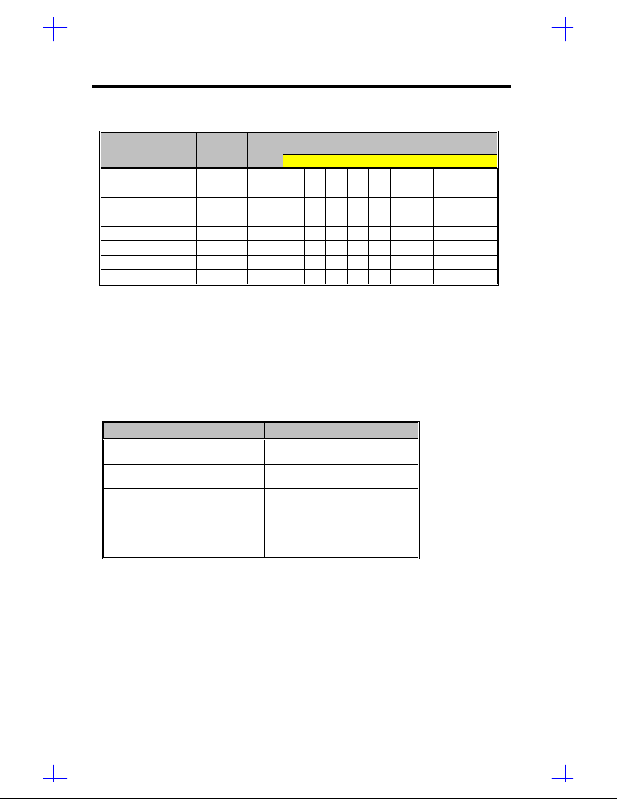
Table 1-8 shows the video display modes using 45ns video RAM.
Table 1-8 Video Display Modes
Display
Resolution
Refresh
Rate
Horizontal
Frequency
Pixel
Clock Colors (Bits / Pixel)
(Hz) (KHz) (MHz) 1MB DRAM 2MB DRAM
640*480 60 31.4 25.2 4 8 16 24 32 4 8 16 24 32
640*480 60 31.4 25.2
ü ü ü ü
-
ü ü ü ü ü
640*480 72 37.7 31.2
ü ü ü ü
-
ü ü ü ü ü
640*480 75 37.5 31.5
ü ü ü ü
-
ü ü ü ü ü
640*480 90 47.9 39.9
ü ü ü
- -
ü ü ü
- -
640*480 100 52.9 44.9
ü ü ü
- -
ü ü ü ü
-
800*600
48 int.
33.8 36.0 -
ü ü
- - -
ü ü ü
-
800*600 56 35.1 36.0
ü ü ü
- -
ü ü ü ü
-
800*600 60 37.8 40.0
ü ü ü
- -
ü ü ü
- -
800*600 70 44.5 44.9
ü ü ü
- -
ü ü ü
- -
800*600 72 48.0 50.0
ü ü ü
- -
ü ü ü
- -
800*600 75 46.8 49.5
ü ü ü
- -
ü ü ü
- -
800*600 90 57.0 56.6
ü ü
- - -
ü ü
- - -
800*600 100 62.5 67.5
ü ü
- - -
ü ü
- - -
1024*768
43 int.
35.5 44.9
ü ü
- - -
ü ü ü
- -
1024*768 60 48.3 65.0
ü ü
- - -
ü ü ü
- -
1024*768 70 56.4 75.0
ü ü
- - -
ü ü ü
- -
1024*768 72 58.2 75.0
ü ü
- - -
ü ü ü
- -
1024*768 75 60.0 78.8
ü ü
- - -
ü ü ü
- -
1024*768 90 76.2 100 - - - - -
ü ü
- - -
1024*768 100 79.0 110 - - - - -
ü ü
- - -
1152*864
43 int.
45.9 65.0
ü ü
- - -
ü ü
- - -
1152*864
47 int.
44.8 65.0
ü ü
- - -
ü ü
- - -
1152*864 60 54.9 80.0
ü ü
- - -
ü ü
- - -
1152*864 70 66.1 100 - - - - -
ü ü
- - -
Page 12
1-12 Service Guide
Table 1-8 Video Display Modes (continued)
Display
Resolution
Refresh
Rate
Horizontal
Frequency
Pixel
Clock Colors (Bits / Pixel)
(Hz) (KHz) (MHz) 1MB DRAM 2MB DRAM
1152*864 75 75.1 110 - - - - -
ü ü
- - -
1152*864 80 75.1 110 - - - - -
ü ü
- - -
1280*1024
43 int.
50.0 80.0
ü
- - - -
ü ü
- - -
1280*1024
47 int.
50.0 80.0
ü
- - - -
ü ü
- - -
1280*1024 60 63.9 110 - - - - -
ü ü
- - -
1280*1024 70 74.6 126 - - - - -
ü ü
- - -
1280*1024 74 78.8 135 - - - - -
ü ü
- - -
1280*1024 75 79.9 135 - - - - -
ü ü
- - -
int. - interlaced
1.5.5 Parallel Port Configurations
The onboard parallel port interface supports a 25-pin D-type connector. The port functions in
different operation modes and is adjustable to select LPT1, LPT2, and LPT3 by changing the
CMOS settings in the BIOS Utility.
Table 1-9 lists the operation mode settings and their corresponding functions.
Table 1-9 Parallel Port Operation Mode Settings
Setting Function
Standard Parallel Port (SPP) Allows normal speed operation but in
one direction only
Enhanced Parallel Port (EPP 1.7/1.9) Allows bidirectional parallel port
operation at maximum speed
Extended Capabilities Port (ECP) Allows parallel port to operate in
bidirectional mode and at a speed
higher than the maximum data
transfer rate
Standard and Bidirectional Allows normal speed operation in a
two-way mode
1.5.6 Serial Port Configurations
The system board has two high-speed 9-pin D-type serial ports. These ports are NS16C550compatible UARTs with 16-byte FIFO send/receive capability. The port functions are software
adjustable to select COM1, COM2, COM3, and COM4.
1.5.7 IDE Interface Configurations
The system board includes PCI enhanced local bus IDE interfaces that accommodate up to four
IDE devices. The interfaces functions as PCI bus master IDE and support PIO mode-4 and DMA
mode-2. The interfaces are fully compatible with ANSIS ATA Rev. 3.0 specifications and ATAPI
specifications.
Page 13
System Introduction 1-13
1.5.8 Memory Address Map
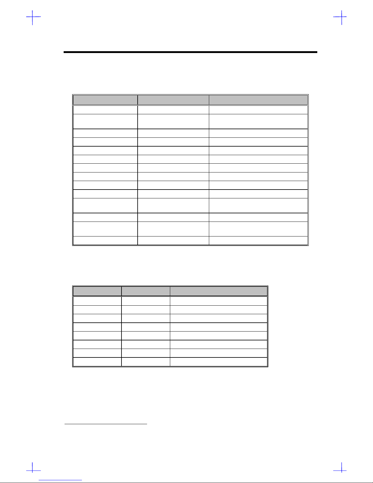
Table 1-10 Memory Address Map
Address Size Function
0000000 ~ 009FFFF 640 KB system memory Onboard DRAM
00A0000 ~ 00BFFFF 128 KB video RAM Reserved for graphics display buffer,
non-cacheable
00C0000 ~ 00C7FFF 32 KB for VGA BIOS Reserved for onboard VGA
00C8000 ~ 00CFFFF 32 KB I/O expansion ROM Reserved for ROM on I/O adapters
00D0000 ~ 00D3FFF 16 KB I/O expansion ROM Reserved for ROM on I/O adapters
00D4000 ~ 00D7FFF 16 KB I/O expansion ROM Reserved for ROM on I/O adapters
00D8000 ~ 00DBFFF 16 KB I/O expansion ROM Reserved for ROM on I/O adapters
00DC000 ~ 00DFFFF 16 KB I/O expansion ROM Reserved for ROM on I/O adapters
00E0000 ~ 00E7FFF 32 KB for SCSI BIOS Reserved SCSI BIOS
00E8000 ~ 00EFFFF 32 KB Reserved onboard (video RAM BIOS)
00F0000 ~ 00FFFFF 64 KB BIOS System ROM BIOS (ROM)
System RAM BIOS (DRAM)
0100000 ~ 0F9FFFF System memory Onboard DRAM
0FA0000 ~ 0FFFFFF 384 KB I/O card memory Reserved for memory map I/O card,
non-cacheable
1000000 ~ Upper limit1System memory Onboard DRAM
1.5.9 PCI INTx# Map
Table 1-11 PCI INTx# Map
PCI Bus# PCI INTx PCI Device
PCI Bus 0 INTA AIC-7880 SCSI; PCI slot s1, 2
INTB PCI slots 1, 2
INTC PCI slots 1, 2
INTD PCI slots 1, 2
PCI Bus 1 INTA PCI slots 3, 4, 5
INTB PCI slots 3, 4, 5
INTC PCI slots 3, 4, 5
INTD PCI slots 3, 4, 5
1
Upper limit means the maximum size of main memory.
Page 14
1-14 Service Guide
1.5.10 Interrupt Channels Map
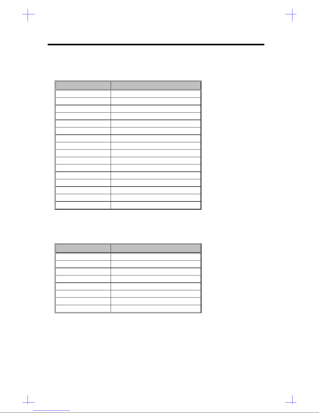
Table 1-12 Interrupt Channels Map
IRQ System Device
IRQ0 Timer output 0
IRQ1 Keyboard
IRQ2 Reserved
IRQ3 Serial port 2
IRQ4 Serial port 1
IRQ5 Reserved
IRQ6 Diskette drive
IRQ7 Parallel port
IRQ8 Real-time clock
IRQ9 Reserved
IRQ10 Reserved
IRQ11 Reserved
IRQ12 PS/2 mouse
IRQ13 Math coprocessor
IRQ14 IDE hard disk
IRQ15 Reserved
1.5.11 DMA Channels Map
Table 1-13 DMA Channels Map
Channel Function
0 Available
1 Available
2 Floppy Controller
3 Available
4 Cascaded
5 Available
6 Available
7 Available
Page 15
System Introduction 1-15
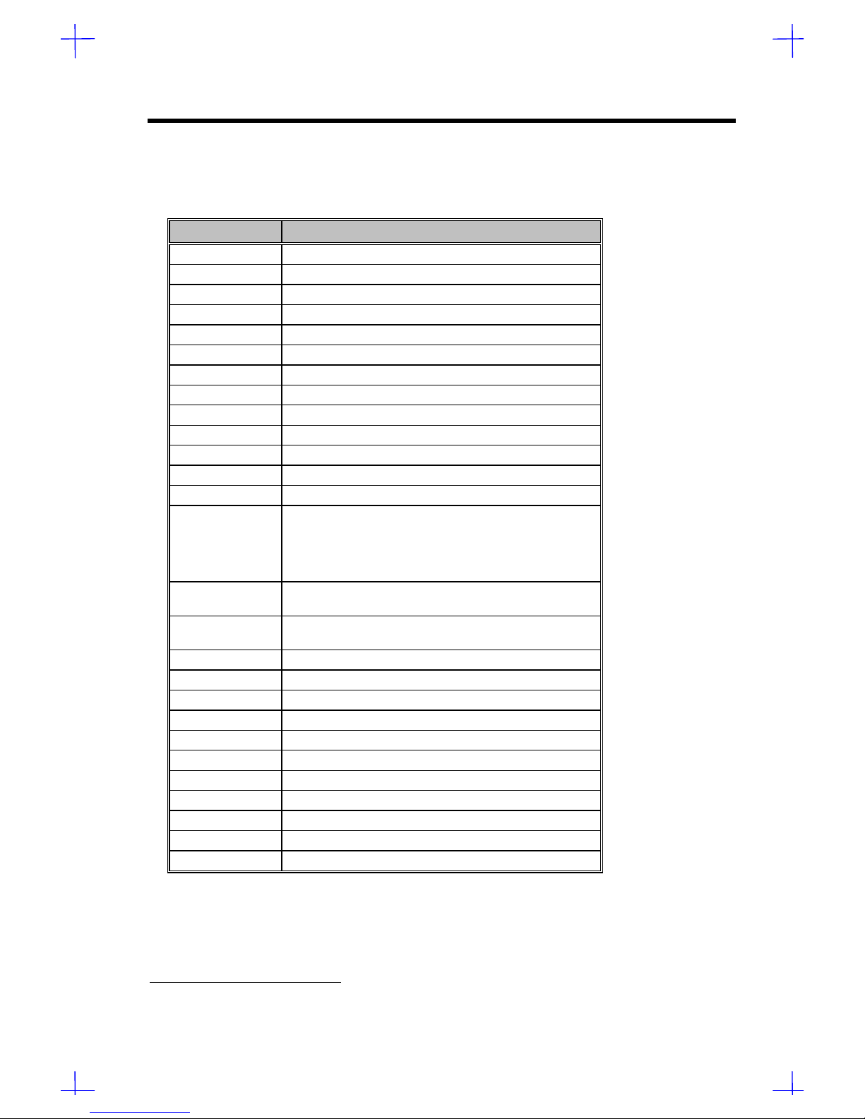
1.5.12 I/O Address Map
Table 1-14 I/O Address Map
Hex Range Device
000 ~ 01F DMA controller 1, (8237)
020 ~ 027 Interrupt controller 1, (8259)
030 ~ 037 Interrupt controller 1, (8259)
040 ~ 047 System timer (8254-1)
050 ~ 057 System timer (8254-1)
060 ~ 06F Keyboard controller (8742)
070 ~ 07F Real-time clock, NMI mask
080 ~ 09F DMA page register 74LS612, speed status register
0A0 ~ 0BF Interrupt controller 2, (8259)
0C0 ~ 0DF DMA controller 2, (8237)
0F0 Clear math coprocessor busy
0F1 Reset math coprocessor
0F8 ~ 0FF Math coprocessor
4F0
1
Onboard VGA enabled/disable
Flash ROM programming
RDM reset
DMA channel 1 selection
DMA channel 3 selection
4F1
1
ASM data read/write port
IRQ mapper read/write port
4F2
1
ASM index write port
IRQ mapper index read/write port
0CF8 PCI configuration address regulation
0CFC PCI configuration data regulation
1F0 ~ 1F7 Hard disk
278 ~ 27F Parallel port 2
2F8 ~ 2FF Serial port 2
378 ~ 37F Parallel port 1
3B0 ~ 3BF Monochrome display
3C0 ~ 3CF EGA, VGA, SVGA
3D0 ~ 3DF CGA, VGA, SVGA
3F0 ~ 3F7 Diskette drive controller
3F7 ~ 3FF Serial port 1
1
Special I/O port
Page 16

1-16 Service Guide
1.6 System Block Diagram
Figure 1-7 System Block Diagram
Page 17

System Introduction 1-17
Figure 1-8 System Clock Block Diagram
Page 18

1-18 Service Guide
1.7 Operation Theory
1.7.1 Memory Address Structure
M9B is a Pentium Pro system based on 440FX PCIset supports 4GB of addressable memory
space and 64 KB of addressable I/O space. The Pentium Pro processor family supports
addressing of memory ranges larger than 4GB via the REQa[4:0]# signals (see Chapter 4 for
details). The PMC claims any access over 4GB by terminating transaction (without forwarding it to
the PCI bus). Writes are terminated simply by dropping the data and the PMC returns all zeros for
reads.
15M1M640K512K0MExtended
ISA
Memory
DOS
Compatible
Memory
and
Buffer Area
(128KB)
Optional
Fixed
Memory
Hole
(128KB)
DOS Area
(512KB)
768KB640KB512KB
Standard
PCI/ISA
Video
Memory
Area
(128KB)0C0000h0BFFFFh0A0000h09FFFFh080000h07FFFFh000000h
Figure 1-9 Memory Address Structure
DOS Area (0000-9FFFFh)
The DOX area is 640KB in size and it is further devided into two parts. The 512KB area at 0 to
7FFFFh is always mapped to the main memory controlled by the PMC, while the 128KB address
range from 080000 to 09FFFFh can be mapped to PCI or to main DRAM. By default this range is
mapped to main memory and can be diclared as a main memory hole by BIOS CMOS setup.
Video Buffer Area (A0000-BFFFFh)
The 128KB graphics adapter memory region in normally mapped to a video device on the PCI bus
(typically VGA controller). This region is also the default region for SMM space.
Page 19

System Introduction 1-19
Expansion Area (C0000-DFFFFh), Extended System BIOS Area (E0000-EFFFFh)
This two areas can be assigned as shadow or disable(read/write for other use, not shadow for
expansion ROM BIOS use) states by BIOS CMOS setup. By manipulating the shadow attributes,
the PMC can “shadow” the expansion ROM BIOS into the main DRAM Typically, these blocks
are mapped through the PCI bridge to ISA space. Memory that is disabled is not remapped.
System BIOS Area (F0000-FFFFFh)
This area is a single 64KB segment. This segment can be assigned as shadow or disable
(read/write for other use, not shadow for system BIOS use) states by BIOS CMOS setup. By
manipulating the shadow attributes, the PMC can “shadow” system BIOS into the main DRAM.
Memory that is disabled is mot remapped.
Extended Memory Area
This memory area covers 100000h (1 MB) to FFFFFFFFh (4GB minus 1) address range and it is
devided into the following regions:
• DRAM memory from 1 MB to a Top of Memory
• PCI memory space from the Top of Memory to 4GB with two specific ranges
• APIC Configuration Space from FEC00000h (4GB minus 20 MB) to FEC0_FFFFh
• High BIOS area from 4GB to 4GB minus 2 MB
DRAM memory from 1 MB to a Top of Memory
The address range from 1 MB to the top of main memory is mapped to main DRAM address range
controlled by PMC. All accesses to addresses within this range are forwarded by the PMC to the
DRAM unless a hole in this range is created by BIOS CMOS setup.
PCI memory space from the Top of Memory to 4GB with two specific ranges
The address range from the top of main DRAM to 4GB is normally mapped to PCI. The PMC
forwards all accesses within this address range to PCI.
There are two sub-ranges within this address range defined as APIC configuration space and high
BIOS address range.
APIC Configuration Space from FEC00000h (4GB minus 20 MB) to FEC0_FFFFh
This range is reserved for APIC(Advanced Programmable Interrupt Controller) configuration space
which includes the default I/O APIC configuration space.
The Pentium Pro accesses to the Local APIC configuration space do not result in external bus
activity since the Local APIC configuration space is internal to the Pentium Pro CPU.
Page 20

1-20 Service Guide
High BIOS area from 4GB to 4GB minus 2 MB
The top 2 MB of the Extended Memory Region is reserved for System BIOS (High BIOS),
extended BIOS for PCI devices, and the A20 alias of the system BIOS. The CPU begins
execution from the High BIOS after reset. This region is mapped to the PCI so that the upper
subset of this region is aliased to 16 MB minus 256KB range.
Memory shadowing
A block of memory that can be desiged as “shadowed” into PMC DRAM memory. Typically this is
done to allow ROM code to execute more rapidly our of main DRAM. ROM is used as a read-only
during the copy process while DRAM at the same time is designated write-only. After copying, the
DRAM is designated read-only so that ROM is shadowed. CPU bus transactions are routed
accordingly. The PMC does not respond to transactions originating from the PCI or ISA masters
and targeted at shadowed memory blocks.
1.7.2 System Arbitration Logic
P6
CPU
82374SB
ESC
82439HX
EISA Master
& ISA DMA
BOFF#
MREQ[2:0]#
DRQ[7:0]
DACK[7:0]#MACK[2:0]#
PCEBGNT#PCEBREQ#
EISAHOLD
EISAHOLDA
PHLD#
PHLDA#
82375SB
PCEB
PAL
Figure 1-10 System Arbitration Logic
The master device request from ISA and EISA Bus are centralized arbitrated by PCEB, then
convey to 82439HX. The ESC generates the EISA Master Acknowledge (MACK[2:0]) signals in
response to the Master Request (MREQ[2:0]) signals from EISA master devices. The ESC has a
DMA controller includes the DISA Bus arbiter which works with the 82439HX’s PCI bus arbiter.
This arbiter determines which requester from among the requesting ISA Bus DMA master, EISA
Bus master, the PCI Bus, or Refresh should have the bus.
Page 21

System Introduction 1-21
The 82439HX’s PCI bus arbiter allows PCI peer-to peer traffic concurrent with CPU main
memory/second level cache cycles. The arbiter supports five PCI masters. REQ[3:0]#/GNT[3:0]#
are used by PCI master devices. PHLD#/PHLDA# are the arbitration request/grant signals for the
PCEB and provide guaranteed access time capability for ISA masters. PHLD#/PHLDA# also
optimize system performance base on PCEB know policies. The arbitration mechanism is
enhanced with a multi-transaction timer mechanism. This feature improves the PCI bandwidth
allocation to short bursts, and important consideration for example, with typical video capture
devices.
1.7.3 Cache Organization Logic
TXC
PBSRAM
CHIP
(32K*32X4)
HA[18:3]
Figure 1-11 Cache Organization Logic
The 82439HX integrates a high performance write-back second level cache controller using
internal/external tags and provides a full first-level and second-level cache coherency mechanism.
The second level cache is direct mapped, non-sectored, and supports a write-back cache policy.
Cache lines are allocated on read misses (not write allocate).
The second-level cache is configured to support 512-KB cache using synchronous pipeline burst
SRAMs. A second level cache line is 32-byte wide, and the second level cache contains 16K
lines. Valid and modified status bits are kept on a per-line basis. Cacheability of the entire
memory space in first-level cache is supported. The memory space cacheability for the secondary
cache is 512 MB of the system memory. See Figure 1-12.
Page 22

1-22 Service Guide
512KBytes(External SRAMs) 0Tag 0 A(28:19)Tag
(Internal to TXC)
16KBytes
Figure 1-12
1.7.4 Interrupt Distribution Logic
PCI Bus 1 Slots
XD[7:0]
IDXA[7:0]
SINTA#SINTB#SINTC#SINTD#
IRQ Mapper
PLSI
INTA#INTB# INTC#INTD#INTA#INTB#INTC#INTD#INTA#INTB#INTC#INTD#
ADR04F1#
LS244
INDEX_W#
LS273
XD[7:0]XD[7:0]
IDXA[3:0]
ADR04F2#
SIRQ3,4,9:12,14,15
Figure 1-13 Interrupt Distribution Logic
The ESC provides an ISA compatible interrupt controller. The interrupts from first-level PCI bus
are routed to ESC while the interrupts from second-level PCI bus are routed to ESC via a IRQ
mapper PLCI. Anyhow, all these interrupts are processed in term of the way of ISA IRQs.
Page 23

System Introduction 1-23
1.7.5 Dual-processor Operating Logic
ESC
8259APCIINIT[5:1]#
IRQ3,4,9:12,14,15
I/O
APICINTR
Figure 1-14 Dual-processor Operating Logic
The MP specification defines three different interrupt modes as follows:
1. PIC Mode - effectively bypasses all APIC component and forces the system to operate in
single-processor mode.
2. Virtual Wire Mode - uses an APIC as a virtual wire, but otherwise operates the same as PIC
Mode.
3. Symmetric I/O Mode - enables the system to operate with more than one processor.
In M9A system, the virtual wire mode is adapted when only one processor installed. In virtual wire
mode, the 8259A-equivalent PIC fields all interrupts, and the local APIC becomes a virtual wire,
which delivers interrupts from the PIC to the processor via the local APIC’s local interrupt 0
(LINTIN0). The LINTIN0 pin of the local APIC is programmed as ExtINT, specifying to the APIC
that the PIC is to serve as an external interrupt controller. Whenever the local APIC finds that a
particular interrupt is of type ExtINT, it asserts the ExtINTA transaction along with the PINT
interrupt to the processor. In this case, the I/O APIC is not used.
In symmetric I/O Mode, the I/O interrupt are generated by the I/O APIC. All 8259 interrupt lines
are either masked or work together with the I/O APIC in a mixed mode. This hardware supports a
mode of operation in which the system can switch easily to symmetric I/O Mode from virtual wire
mode.
Page 24

1-24 Service Guide
1.8 Power Management
1.8.1 Power Management Modes
The system has three power management modes: normal mode, IDE hard disk standby mode,
and system suspend mode.
Normal Mode
The normal operating mode of the system.
IDE Hard Disk Standby Mode
The IDE hard disk standby mode that controls ATA power-management-compliant hard disk
drives. This feature allows the device to enter into IDE hard disk standby mode after a specified
HDD non-activity period, and to return to normal mode immediately after a hard disk access.
The IDE hard disk standby mode has the following features:
• HDD power-management timer (1-15 minutes, time step = 1 minute)
• Allows HDD to go into standby mode (for ATA standard interface)
• Resume method: Any IDE HDD activity
System Suspend Mode
This is a fast-on, power-saving mode, allowing the PC to return to full power immediately. It
allows the VGA monitor to enter standby mode and turns off the hard disk drive spindle motor.
Any system activity returns the system to full power.
The system standby mode has the following features:
• Global power-management timer (1-15 minutes, time step = 1 minute)
• HDD goes into standby mode (for ATA standard interface)
• Disables H-sync and V-sync signals to control the VESA DPMS monitor
• LED on the panel flashes at 1.6-second intervals
• Resume method: Activity from keyboard, mouse, or any IRQ/DRQ enabled in the CMOS
Page 25

System Introduction 1-25
1.8.2 Power Saving Flowchart
One of the monitored system events is activated All monitored system events idle untilSystem Suspend Timer timeoutSystem SuspendMode Mode
Figure 1-15 Power Saving Flowchart
Page 26
1-26 Service Guide
1.10 Power Requirements
The specific housing configuration of the M9A system determines the total power consumption
required by the system.
1.10.1 525W Power Supply
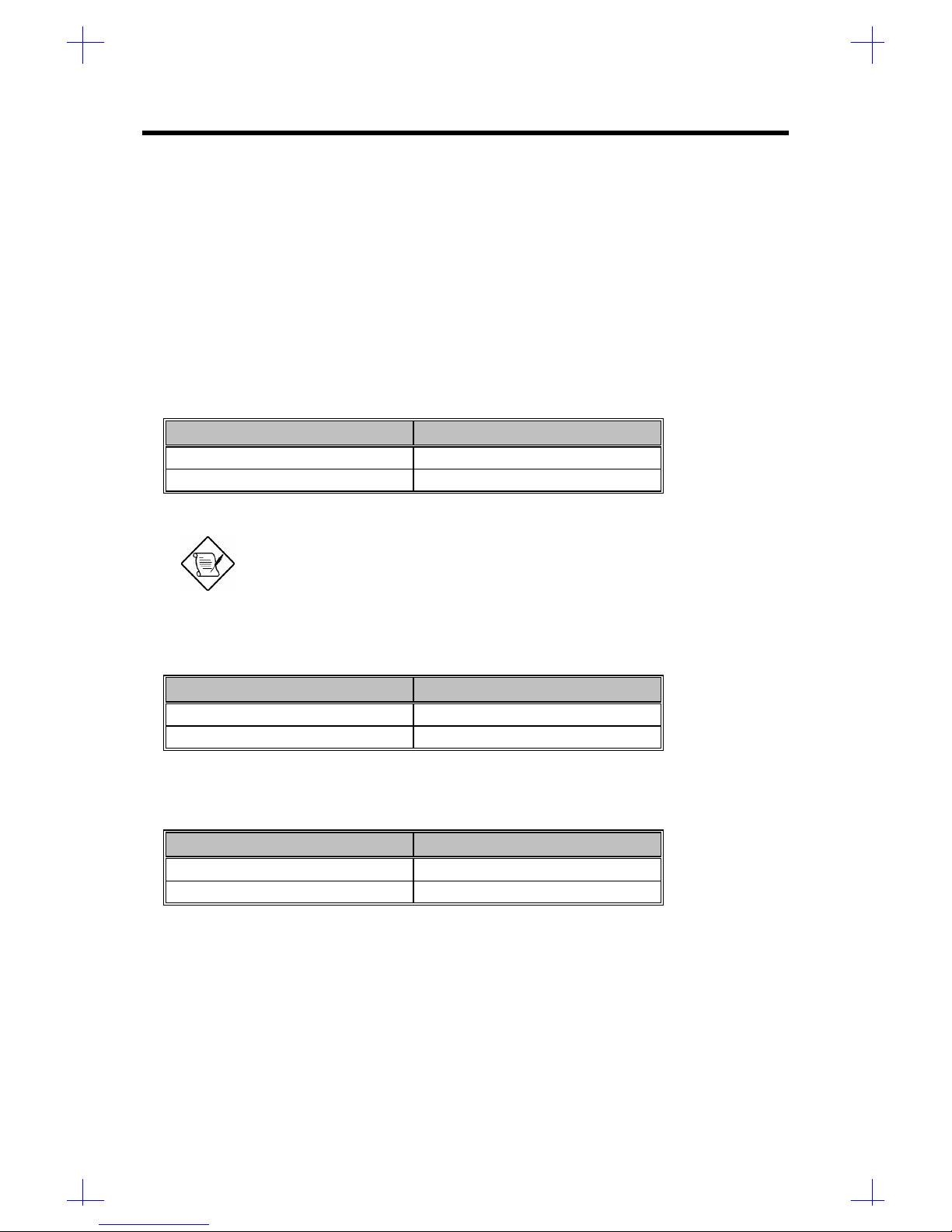
Input Requirements
The power supply must be connected to a single-phase power system.
Table 1-15 525W SPS Input Frequency
Nominal Frequency Frequency Variation Range
50 Hz 60 Hz
47 Hz ~53 Hz 57 Hz ~ 63 Hz
Waveform harmonic distortion is less than 5%.
The power supply must operate at above frequency with both
100~120/200~240 VRMS.
Table 1-16 525W SPS Input Voltage
Nominal Voltage Variation Range
100 ~ 120 VRMS 90 ~ 132 VRMS
200 ~ 240 VRMS 180 ~ 264 VRMS
Table 1-17 525W SPS Input Current
Input Current Measuring Range
12A 90 ~ 132 VRMS
7A 180 ~ 264 VRMS
Regulator Efficiency: 65% minimum, measuring at maximum load, applying nominal line.
Page 27
System Introduction 1-27
Output Requirements
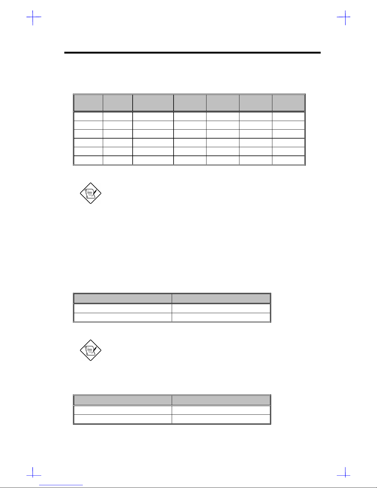
Table 1-18 525W SPS Output Rating
Output Nominal Regulation Ripple Noise Minimum Maximu
m
1 +5.1V +2%, -2% 100mV 10A 57A
2 +12V A +5%, -5% 180mV 180mV – 9A
3 +12V B +5%, -5% 180mV 180mV – 8A
4 -12V +10%, -10% 120mV 120mV – 0.6A
5 -5V +10%, -10% 120mV 120mV – 0.3A
6 +3.3V +2%, -2% 66mV 66mV – 11A
Ripple and noise bandwidth from 10 Hz to 20 MHz.
When AC power is on, +12V should provide 10A surge current for
the first 20 seconds. This regulation should be within -6% and
+7%.
1.10.2 350W Power Supply
Input Requirements
The power supply must be connected to a single-phase power system.
Table 1-19 350W SPS Input Frequency
Nominal Frequency Frequency Variation Range
50 Hz 47 Hz ~ 53 Hz
60 Hz 57 Hz ~ 63 Hz
Waveform harmonic distortion is less than 5%.
The power supply must operate at above frequency with both
100~120/200~240 VRMS.
Table 1-20 350W SPS Input Voltage
Nominal Voltage Variation Range
100 ~ 120 VRMS 90 ~ 132 VRMS
200 ~ 240 VRMS 180 ~ 264 VRMS
Page 28
1-28 Service Guide
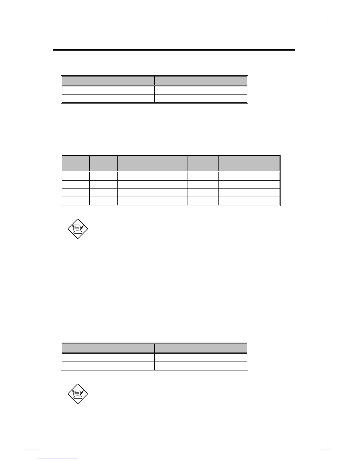
Table 1-21 350W SPS Input Current
Input Current Measuring Range
8A 90 ~ 132 VRMS
4A 180 ~ 264 VRMS
Regulator Efficiency: 70% minimum, measuring at maximum load, applying nominal line.
Output Requirements
Table 1-22 350W SPS Output Rating
Output Nominal Regulation Ripple Noise Minimum Maximu
m
1 +5V +4%, -3% 50mV 100mV 5A 43A
2 -5V +10%, -8% 100mV 200mV 0A 1A
3 +12V +5%, -4% 120mV 200mV 0A 10A
4 -12V +10%, -9% 120mV 200mV 0A 1A
Ripple and noise bandwidth from DC to 20 MHz.
When AC power is on, +12V should provide 13.7A surge current.
This regulation should be within -6% and +7%.
Regulation: The total voltage regulation for each level is calculated in terms of the hand of
voltage defined by the maximum positive and negative excursions (from nominal)
that occur.
1.10.3 200W Power Supply
Input Requirements
The power supply must be connected to a single-phase power system.
Table 1-23 200W SPS Input Frequency
Nominal Frequency Frequency Variation Range
50 Hz 47 Hz ~ 53 Hz
60 Hz 57 Hz ~ 63 Hz
Waveform harmonic distortion is less than 5%.
The power supply must operate at above frequency with both
Page 29
System Introduction 1-29
100~120/200~240 VRMS.
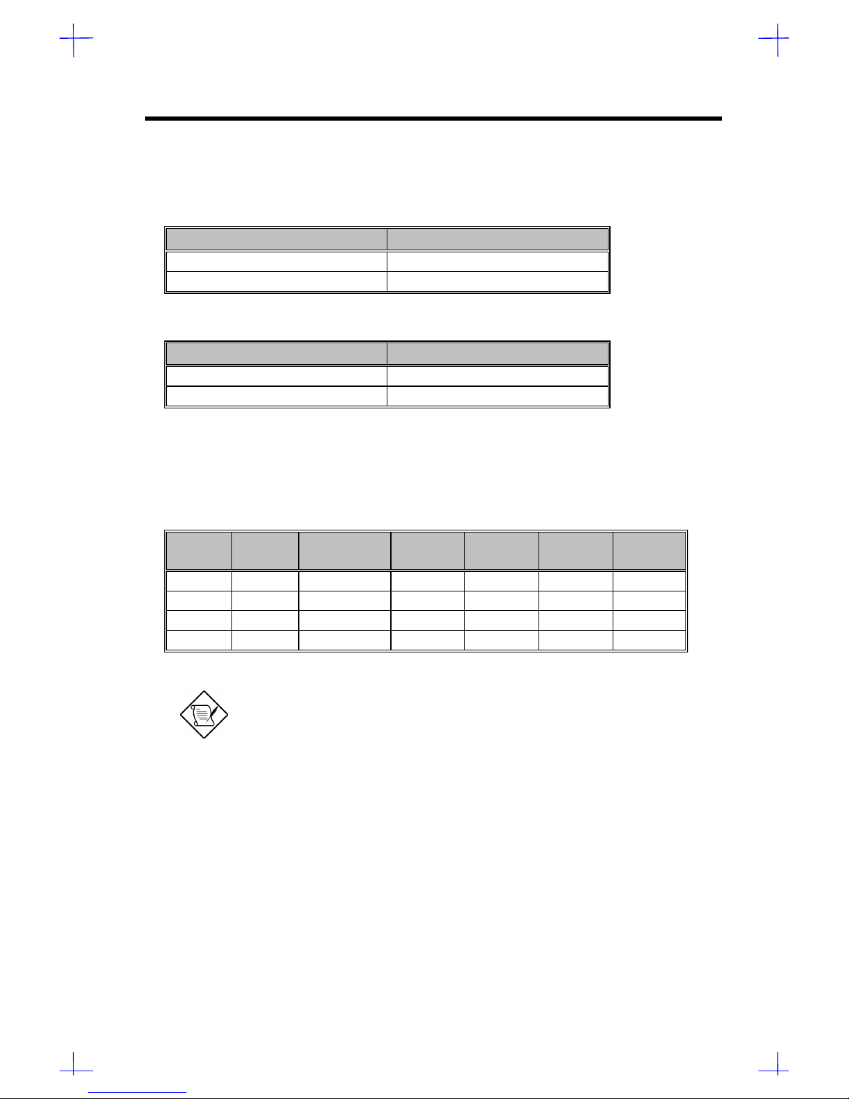
Table 1-24 200W SPS Input Voltage
Nominal Voltage Variation Range
100 ~ 120 VRMS 90 ~ 132 VRMS
200 ~ 240 VRMS 180 ~ 264 VRMS
Table 1-25 200W SPS Input Current
Input Current Measuring Range
8A 90 ~ 132 VRMS
4A 180 ~ 264 VRMS
Regulator Efficiency: 65% minimum, measuring at maximum load, applying nominal line.
Output Requirements
Table 1-26 200W SPS Output Rating
Output Nominal Regulation Ripple Noise Minimum Maximu
m
1 +5V +5%, -4% 50mV 100mV 1.5A
2 -5V +10%, -8% 150mV 200mV 0A 0.5A
3 +12V +5%, -4% 100mV 200mV 0.2A 8A
4 -12V +10%, -8% 200mV 200mV 0A 0.5A
Ripple and noise bandwidth from DC to 20 MHz.
When AC power is on, +12V should provide 10A surge current for
the first 10 seconds. This regulation should be within -6% and
+7%.
Page 30
1-30 Service Guide
1.11 Mechanical Specifications
1.11.1 IDUN Housing
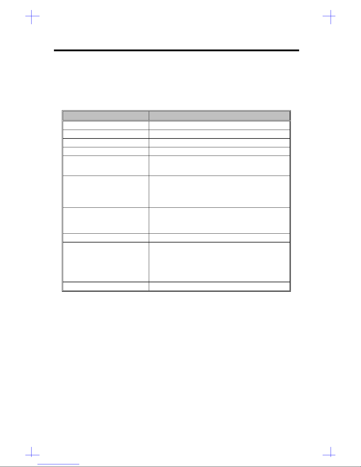
Table 1-27 IDUN Housing Specifications
Item Description
Dimensions
593 mm (h) x 596 mm (d) x 180 mm (w)
Spacing between adapter cards
0.8 inch
Net weight
17.5 kg
Expansion slots
11
Drive Bays
One 3.5-inch external bay
Three 5.25-inch external bays
Eight 3.5-inch, 1.6-inch high internal bays
Major subassembly support
Major subassemblies are rigidly held in place by frame
components. Adequate clearances are provided so that
cards can be installed and removed without bending or
forcing. All other components such as SPS and FDD can
be assembled easily.
Circuit card support
Circuit cards plugged into the system board are supported
by a card edge connector, the card end bracket, and by a
card edge guide supporting the card edge from the farthest
end bracket (if the card conforms to the full length).
Metal finish
All metal surfaces are plated or equivalent treatment
Color/Paint
Units delivered in specified MCS colors. Paint samples
supplied to the vendor as required.
Lower case : Metal
Left cover : Metal
Frame : Metal
Right cover : Metal
Case finish
All surfaces are textured or equivalent treatment
Page 31

System Introduction 1-31
1.11.2 IDATX Housing
Table 1-28 IDATX Housing Specifications
Item Description
Dimensions
400 mm (h) x 454 mm (d) x 190 mm (w)
Spacing between adapter cards
0.8 inch
Net weight
7 kg
Expansion slots
7
Drive Bays
Two 3.5-inch external bays
Three 5.25-inch external bays
Major subassembly support
Major subassemblies are rigidly held in place by frame
components. Adequate clearances are provided so that
cards can be installed and removed without bending or
forcing. All other components such as SPS and FDD can
be assembled easily.
Circuit card support
Circuit cards plugged into the system board are supported
by a card edge connector, the card end bracket, and by a
card edge guide supporting the card edge from the farthest
end bracket (if the card conforms to the full length).
Metal finish
All metal surfaces are plated or equivalent treatment
Color/Paint
Units delivered in specified MCS colors. Paint samples
supplied to the vendor as required.
Upper case : MCS-002 color
Bezel : MCS-002 color
Frame : Zinc metal
Case finish
All surfaces are textured or equivalent treatment
Page 32
C h a p t e r 3
BIOS Setup Information
BIOS Setup Information 3-1
Most systems are already configured by the manufacturer or the dealer. There is no need to run
Setup when starting the computer unless you get a configuration error. The Setup program loads
configuration values into the battery-backed nonvolatile memory called CMOS RAM. This
memory area is not part of the system RAM. If you repeatedly receive Run Setup messages, the
battery may be bad. In this case, the system cannot retain configuration values in CMOS.
3.1 Entering Setup
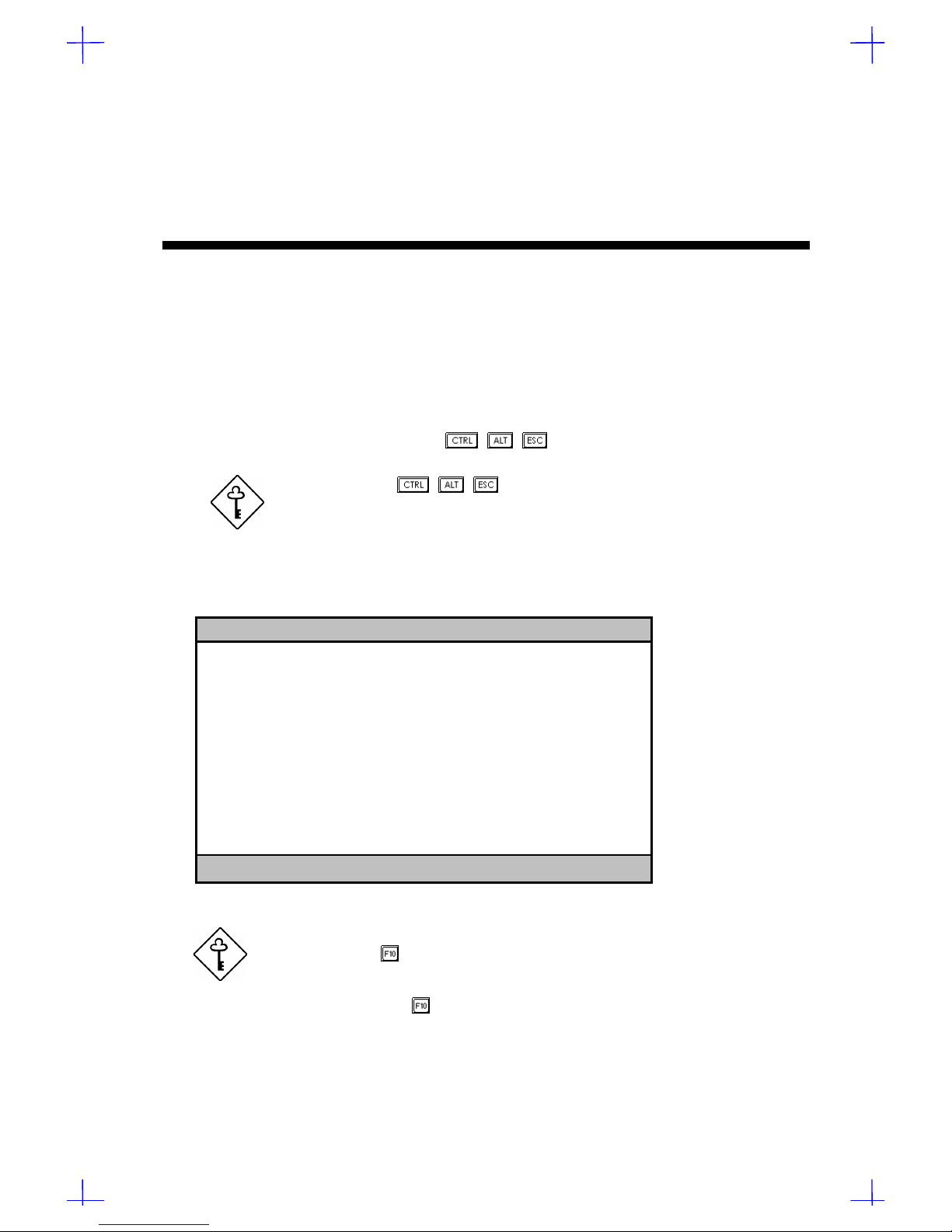
To enter Setup, press the key combination + +
.
You must press + + while the system is booting. This
key combination does not work during any other time.
The BIOS Utility main menu then appears:
BIOS Utility
Basic System Configuration
Advanced System Configuration
PCI System Configuration
Non-PnP ISA Card Configuration
System Security
Remote Diagnostic Configuration
Load Setup Default Settings
↑↓ = Move Highlight Bar, ↵ = Select, Esc = Exit and Reboot
If the system does not boot after you made changes in the CMOS
settings, press then power on the system to load the bootable
settings.
Make sure to keep pressed before system power on until the
execution of the power-on self-tests (POST).
Page 33
3-2 Service Guide
The parameters on the following screens show default values.
These values may not be the same as those in your system.
The grayed items (denoted with asterisks) on the screens have
fixed settings and are not user-configurable.
3.2 Basic System Configuration
Select Basic System Configuration to input configuration values such as date, time, and disk
types.
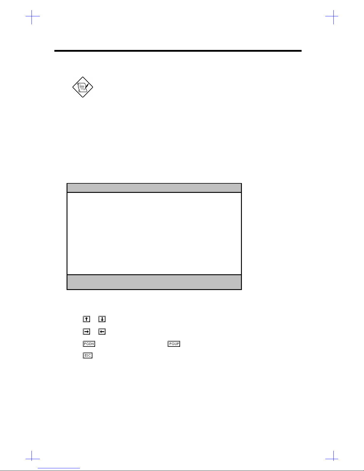
The following screen shows the Basic System Configuration menu.
Basic System Configuration Page 1/2
Date ...................... [MM/DD/YY]
Time ...................... [HH:MM:SS]
Diskette Drive A .......... [xx-MB xx-inch]
Diskette Drive B .......... [xx-MB xx-inch]
Cylinder Head Sector
Hard Disk 0 (xxx MB) ..... [Auto] xx xx xx
Hard Disk 1 (xxx MB) ..... [Auto] xx xx xx
Base Memory ............... [ xxx] KB
Extended Memory ........... [ xxx] KB
Total Memory .............. [ xxxx] KB
Math Coprocessor .......... [ Installed ]
Video Display ............. [VGA/EGA]
↑↓ = Move Highlight Bar, → ← = Change Setting
PgDn/PgUp = Move Screen, F1 = Help, Esc = Exit
The command line at the bottom of the menu tells you how to highlight items, change settings, and
move from one screen to another.
1. Press or on the cursor-edit keypad to highlight the desired parameter.
2. Press or to select the desired option for a parameter.
3. Press to move to the next page or to return to the previous page.
4. Press to exit the configuration menu.
Page 34

BIOS Setup Information 3-3
The following screen shows page 2 of the Basic System Configuration menu.
Basic System Configuration Page 2/2
Communication Settings
Baud Rate ...................... [9600] bps
Parity ......................... [None]
Stop Bits ...................... [1] Bits
Data Length .................... [8] Bits
IDE Features
Hard Disk Block Mode ........... [Disabled]
Hard Disk Size > 504MB ......... [Disabled]
Large Memory Support Mode ......... [ Normal ]
Num Lock After Boot ............... [Enabled ]
Memory Test ....................... [Disabled]
Auto Configuration Mode ........... [Enabled ]
Fast Boot Mode .................... [Enabled ]
↑↓ = Move Highlight Bar, → ← = Change Setting
PgDn/PgUp = Move Screen, F1 = Help, Esc = Exit
The following sections explain the different parameters and their settings.
3.2.1 Date and Time
The real-time clock keeps the system date and time. After setting the date and time, you need not
enter them every time you turn on the system. As long as the internal battery remains good
(approximately seven years) and connected, the clock continues to keep the date and time
accurately even when the power is off.
Date
Highlight the items on the date parameter and press or to set the date following the monthday-year format.
Valid values for month, day, and year are:
• Month 1 to 12
• Day 1 to 31
• Year 00 to 99
The setting 00 for the Year item represents year 2000.
Time
Highlight the items on the time parameter and press or to set the time following the hourminute-second format.
Valid values for hour, minute, and second are:
• Hour 00 to 23
• Minute 00 to 59
• Second 00 to 59
Page 35

3-4 Service Guide
3.2.2 Diskette Drives
To enter the configuration value for the first diskette drive (drive A), highlight the Diskette Drive A
parameter. Press or key to view the options and select the appropriate value.
The Diskette Drive parameters have the following options:
• [ None ]
• [360 KB, 5.25-inch]
• [1.2 MB, 5.25-inch]
• [720 KB, 3.5-inch]
• [1.44 MB, 3.5-inch]
• [2.88 MB, 3.5-inch]
Follow the same procedure for the Diskette Drive B parameter. Choose None if you do not have a
second diskette drive.
3.2.3 Hard Disk Drives
Move the highlight bar to the Hard Disk 0 parameter to configure the hard disk drive (drive C).
Press or to display the hard disk options with their respective values. Select the option that
corresponds to your hard disk type. Follow the same procedure for the Hard Disk 1 parameter.
Choose None if you do not have a second hard disk drive.
Selecting the “Auto” Option
If you do not know the exact type of your hard disk, select the option Auto. During POST, when
the system performs self-testing and self-initialization before loading the operating system and
applications, the BIOS utility automatically determines the type of your hard disk. You can see the
hard disk values when you enter the BIOS Utility.
Cylinder Head Sector
Hard Disk 0 (xxx MB) . [Auto] xx xx xx
The next time you boot the system, the BIOS utility does not have to auto-configure your hard disk
as it detects the saved hard disk information during POST.
Copy the hard disk drive values and keep them in a safe place in
case you have to reconfigure the disk in the future.
Follow the same procedure to auto-configure other hard disks.
Page 36

BIOS Setup Information 3-5
Selecting the “User” Option
There are cases when you cannot use the option Auto, instead you have to select User. Choose
the User option when you have installed a hard disk that was previously formatted but does not
use the disk native parameters or structure. That is, the disk type may be in the hard disk types
list but the number of cylinders, heads, and sectors differ.
Cylinder Head Sector
Hard Disk 0 (xxx MB) .[Auto] xx xx xx
Follow these steps to configure a hard disk with the User option:
1. Highlight the hard disk parameter.
2. Select the option User then press .
3. Type in the number of cylinders, heads, and sectors of the hard disk under the appropriate
columns.
Be sure to have the correct hard disk information beforehand.
4. Choose YES when asked if you want to save the CMOS data.
3.2.4 System Memory
The system automatically detects the total amount of onboard memory during the POST and sets
the memory parameters accordingly. If you install additional memory, the system automatically
adjusts the Total Memory parameter to display the new memory size.
3.2.5 Communication Settings
The Communication Settings parameters allow you to set the baud rate, parity, stop bit and data
length for the first serial port (COM 1). The values for this parameter are:
• Baud rate : 300 to 38400 bits per second (bps)
• Parity : odd, even, or none
• Stop bit : 1 or 2 stop bits
• Data length : 7- or 8-bit data word
The baud rate maximum value is only for the BIOS POST under
UNIX environment. The system I/O chipset SMC 37C665GT
supports up to 115.2K bps.
Page 37

3-6 Service Guide
3.2.6 IDE Features
Hard Disk Block Mode
This function enhances disk performance depending on the hard disk in use. If you set this
parameter to Enabled, it allows data transfer in block (multiple sectors) by increasing the data
transfer rate to 256 bytes per cycle. If your system does not boot after enabling this parameter,
change the setting to Disabled . This parameter is normally set to Disabled .
Hard Disk Size > 504 MB
This enhanced IDE feature works only under DOS and Windows 3.x environment. If enabled, it
allows you to use a hard disk with a capacity of more than 504 MB. This is made possible through
the Logical Block Address (LBA) mode translation. Other operating systems require this
parameter to be set to Disabled .
To prevent data loss, keep this parameter to Enabled if you are using a hard disk with more than
504 MB capacity and was previously configured through LBA mode. When you use a hard disk
configured through the cylinder-head-sector (CHS) mode, set this parameter to Disabled .
3.2.7 Large Memory Support Mode
This parameter allows the system to support an extended memory higher than 64 MB. Set this
parameter to Advanced if you are working under Windows NT environment and the system
memory size is greater than or equal to 64 MB. Otherwise, set it to Normal.
3.2.8 Num Lock After Boot
This parameter allows you to activate the Num Lock function upon booting. The default setting is
Enabled .
3.2.9 Memory Test
When set to Enabled, this parameter allows the system to perform a RAM test during the POST
routine. When set to Disabled, the system detects only the memory size and bypasses the test
routine. The default setting is Disabled .
This item is fixed to Disabled and is not user-configurable if you enabled the Auto Configuration
Mode and the Fast Boot Mode parameters on page 2 of the Basic System Configuration menu.
See section 3.2.10 and 3.2.11.
3.2.10 Auto-configuration Mode
When enabled, this parameter automatically sets the system configuration values to their
optimized settings. At the same time, it causes the Memory Test parameter to be fixed to
Disabled and the shadow RAM region for system and video BIOS to Enabled. See sections
3.2.9 and 3.3.1.
Set this parameter to Enabled if you do not know the hard disk drive type parameters and the
onboard communication port configuration.
Page 38

BIOS Setup Information 3-7
3.2.11 Fast Boot Mode
When enabled, this parameter allows the system to boot faster by skipping some POST routines.
It bypasses memory test, enables Shadow RAM, and enables primary- and second-level cache.
When set to Enabled, this parameter also causes the Memory Test parameter to be fixed to
Disabled and the shadow RAM regions for system and video BIOS to Enabled . See sections
3.2.9 and 3.3.1.
3.3 Advanced System Configuration
The Advanced System Configuration option allows you to configure the advanced system memory
functions.
Do not attempt to change any setting in the Advanced Configuration
if you are not a qualified technician.
The following screen shows page one of the Advanced System Configuration parameters.
Advanced System Configuration Page 1/1
Shadow RAM
E0000h - FFFFFh (System BIOS) ... [Enabled ]
C0000h - C7FFFh (Video BIOS)..... [Enabled ]
C8000h - CBFFFh ................. [Disabled]
CC000h - CFFFFh ................. [Disabled]
D0000h - D3FFFh.................. [Disabled]
D4000h - D7FFFh ................. [Disabled]
D8000h - DBFFFh ................. [Disabled]
DC000h - DFFFFh ................. [Disabled]
L1 & L2 Cache (CPU Cache) .......... [Enabled ]
Cache Scheme .................... [ Write Back ]
ECC/Parity Mode Selection .......... [ECC (SEC/DED) ]
Memory at 15MB-16MB Reserved for.... [ System ] Use
↑↓ = Move Highlight Bar, → ← = Change Setting
PgDn/PgUp = Move Screen, F1 = Help, Esc = Exit
Page 39

3-8 Service Guide
3.3.1 Shadow RAM
The system reserves 384 KB of random access memory (RAM) for the shadow RAM function.
This parameter has eight range addresses. When you set these addresses to Enabled, the
system BIOS, video BIOS, and I/O ROM functions run directly from the shadow RAM for faster
operation. When you set them to Disabled, the functions run normally from ROM.
The address range E0000h - FFFFFh is for shadowing the system BIOS. This item is always set
to Enabled and is not user-configurable. The address range C0000h - C7FFFh is for shadowing
the video BIOS. This item is fixed to Enabled and is not user-configurable if the Auto
Configuration Mode and the Fast Boot Mode parameters on page 2 of the Basic System
Configuration menu are enabled. Otherwise, you can disable this item.
The remaining address ranges are for I/O ROM functions.
3.3.2 L1 & L2 Cache (CPU Cache)
This parameter enables or disables the first- and second-level cache memory in the Pentium Pro
CPU.
Cache Scheme
This parameter sets the cache to Write-through or Write-back modes. Write-back updates
the cache but not the memory when there is a write instruction. It updates the memory only when
there is an inconsistency between the cache and the memory. Write-through updates both the
cache and the memory whenever there is a write instruction.
3.3.3 ECC/Parity Mode Selection
This parameter allows you to enable or disable the ECC and parity check feature. Fast-page
mode SIMMs with parity supports both ECC and parity mode. EDO SIMMs with parity supports
only ECC mode. You must disable this parameter if you installed SIMMs without parity.
Operation of ECC
This parameter allows you to select the error detection mode. The following are the ECC
operation options.
• None - detects single-bit errors and automatically corrects any error but does not set the
single-bit error flag in the chipset. In this option, the operating system does not receive any
signal even if there are system errors.
• Single-bit - detects single-bit errors, automatically corrects any error, and sets the single-bit
error flag in the chipset. The setting of the single-bit error flag is a signal to the operating
system that ECC detected single-bit errors.
• Multiple-bit - detects multiple-bit errors and sets the multiple-bit error flag in the chipset
but does not correct the errors. The setting of the multiple-bit error flag is a signal to the
operating system that ECC detected multiple-bit errors.
Page 40

BIOS Setup Information 3-9
• Both - detects both single- and multiple-bit errors but corrects only single-bit errors. This
option sets both the single-and multiple-bit flags in the chipset to send signals to the operating
system that ECC detected errors.
3.3.4 Memory at 15MB-16MB
To prevent memory address conflicts between the system and expansion boards, reserve this
memory range for the use of either the system or an expansion board. Before setting this
parameter, check your add-on card manual to determine if your add-on card needs this memory
space. If not, set this parameter to System Use .
3.4 PCI System Configuration
The PCI System Configuration allows you to specify the settings for your PCI devices.
PCI System Configuration Page 1/1
PCI IRQ Setting .......... [Auto]
INTA INTB INTC INTD
PCI Slot 1 ............ [--] [--] [--] [--]
PCI Slot 2 ............ [--] [--] [--] [--]
PCI Slot 3 ............ [--] [--] [--] [--]
PCI Slot 4 ............ [--] [--] [--] [--]
PCI Slot 5 ............ [--] [--] [--] [--]
Onboard VGA ........... [--]
Onboard SCSI .......... [--]
VGA Palette Snoop ........ [Disabled]
On Board SCSI ............ [Enabled ]
Boot Device ........... [Enabled ]
↑↓ = Move Highlight Bar, → ← = Change Setting
PgDn/PgUp = Move Screen, F1 = Help, Esc = Exit
3.4.1 PCI IRQ Setting
This parameter allows for Auto or Manual configuration of PCI devices. If you use plug-andplay (PnP) devices, you can keep the default setting Auto. The system then automatically
configures the PnP devices. If your PCI device is not a PnP, you can manually assign the
interrupt for each device. Refer to your manual for technical information about the PCI card.
When the PCI IRQ Setting is set to Auto, all the IRQ setting fields
become gray and non-configurable.
PCI Slots
These parameters allow you to specify the appropriate interrupt for each of the PCI devices. For
PCI slots 1 and 2 which operate on PCI bus 0, you can assign IRQ3, IRQ4, IRQ5, IRQ7, IRQ9,
IRQ10, IRQ11, IRQ12, IRQ14, and IRQ15.
Page 41

3-10 Service Guide
For PCI slots 3, 4, and 5 which operate on PCI bus 1, you can assign IRQ4, IRQ9, IRQ10, IRQ11,
IRQ12, IRQ14, and IRQ15.
Make sure that the interrupt you assign in any of the PCI slots are
not used by other devices to avoid conflicts.
Press or to move between fields. Press or to select options.
Onboard VGA
This parameter allows you to manually assign the interrupt for the onboard VGA when the PCI IRQ
Setting parameter is set to Manual. This parameter is grayed and not configurable when the PCI
IRQ Setting is set to Auto.
Press or to move between fields. Press or to select options.
Onboard SCSI
This parameter allows you to manually assign the interrupt for the onboard SCSI hard disk when
the PCI IRQ Setting parameter is set to Manual. This parameter is grayed and not configurable
when the PCI IRQ Setting is set to Auto.
Press or to move between fields. Press or to select options.
3.4.2 VGA Palette Snoop
PCI devices support the palette snooping technique that enables the device to control access to
their palette registers. Set this parameter to Enabled to activate the palette snooping function if
both the PCI VGA and the ISA video devices are installed. Check your VGA card manual for
more information about this function.
3.4.3 Onboard SCSI
This parameter allows you to enable or disable the onboard SCSI feature.
Boot Device
This parameter allows you to enable or disable the onboard SCSI boot priority.
Page 42

BIOS Setup Information 3-11
3.5 Non-PnP ISA Card Configuration
The Non-PnP ISA Card Configuration parameters allow you to specify the settings for cards
without the plug-and-play (PnP) feature.
Non-PnP ISA Card Configuration Page 1/2
System Resources Used by Non-PnP ISA Cards
IRQ/DMA
IRQ 00....[---]* IRQ 08.... [---]* DMA 0 ...[No ]
IRQ 01....[---]* IRQ 09.... [No ] DMA 1 ... [No ]
IRQ 02....[---]* IRQ 10.... [No ] DMA 2 ... [---]*
IRQ 03....[No ] IRQ 11.... [No ] DMA 3 ... [No ]
IRQ 04....[No ] IRQ 12.... [No ] DMA 4 ... [---]*
IRQ 05....[No ] IRQ 13.... [---]* DMA 5 ...[No ]
IRQ 06....[---]* IRQ 14.... [---]* DMA 6 ...[No ]
IRQ 07....[No ] IRQ 15.... [No ] DMA 7 ... [No ]
Expansion ROM Region
C8000h - CBFFFh..... [No ] D4000h - D7FFFh ..... [No ]
CC000h - CFFFFh..... [No ] D8000h - DBFFFh ..... [No ]
D0000h - D3FFFh..... [No ] DC000h - DFFFFH ..... [No ]
↑↓ = Move Highlight Bar, → ← = Change Setting
PgDn/PgUp = Move Screen, F1 = Help, Esc = Exit
The items marked No are currently not in use, while those marked
Yes are in use by PnP cards.
The grayed items (denoted with asterisks) have fixed settings and
are not user-configurable.
Non-PnP ISA Card Configuration Page 2/2
I/O Region
100h-10Fh .. [No ] 200h-20Fh . [No ] 300h-30Fh ..[No ]
110h-11Fh .. [No ] 210h-21Fh . [No ] 310h-31Fh ..[No ]
120h-12Fh .. [No ] 220h-22Fh . [No ] 320h-32Fh ..[No ]
130h-13Fh .. [No ] 230h-23Fh . [No ] 330h-33Fh ..[No ]
140h-14Fh .. [No ] 240h-24Fh . [No ] 340h-34Fh ..[No ]
150h-15Fh .. [No ] 250h-25Fh . [No ] 350h-35Fh ..[No ]
160h-16Fh .. [No ] 260h-26Fh . [No ] 360h-36Fh ..[No ]
170h-17Fh .. [No ] 270h-27Fh . [No ] 370h-37Fh ..[No ]
180h-18Fh .. [No ] 280h-28Fh . [No ] 380h-38Fh ..[No ]
190h-19Fh .. [No ] 290h-29Fh . [No ] 390h-39Fh ..[No ]
1A0h-1AFh .. [No ] 2A0h-2AFh . [No ] 3A0h-3AFh ..[No ]
1B0h-1BFh .. [No ] 2B0h-2BFh . [No ] 3B0h-3BFh ..[No ]
1C0h-1CFh .. [No ] 2C0h-2CFh . [No ] 3C0h-3CFh ..[No ]
1D0h-1DFh .. [No ] 2D0h-2DFh . [No ] 3D0h-3DFh ..[No ]
1E0h-1EFh .. [No ] 2E0h-2EFh . [No ] 3E0h-3EFh ..[No ]
1F0h-1FFh .. [---]* 2F0h-2FFh . [No ] 3F0h-3FFh ..[No ]
↑↓ = Move Highlight Bar, → ← = Change Setting
PgDn/PgUp = Move Screen, F1 = Help, Esc = Exit
Page 43

3-12 Service Guide
Refer to your non-PnP ISA card manual when setting the following
parameters.
3.5.1 IRQ/DMA
These items allow you to assign specific IRQ and DMA channels to non-PnP ISA cards. The
system will not use such IRQ and DMA channels when it automatically assigns channels to PnP
cards.
3.5.2 Expansion ROM Region
These items specify the memory regions available for add-on card use. It allows you to manually
assign specific regions to non-PnP cards so that the system will not use those regions anymore
when it automatically configures PnP cards.
3.5.3 I/O Region
The items under this parameter allow you to reserve 16-byte memory address ranges for non-PnP
cards. When the system configures PnP cards, the address ranges that you marked will not be
used anymore.
You can assign memory addresses to non-PnP cards at random as long as you cover the address
range required by the card. For example, for a card that requires 178h-188h address, you have to
set regions 170h-17Fh and 180h-18Fh to Yes.
Page 44

BIOS Setup Information 3-13
3.6 System Security Setup
The Setup program has a number of security features to prevent unauthorized access to the
system and its data.
Enter the Setup program and select System Security. The following screen appears:
System Security Page 1/1
Disk Drive Control
Diskette Drive ............ [ Normal ]
Hard disk Drive ........... [ Normal ]
System Boot Drive ......... [Drive A then C]
Onboard Communication Ports
Serial Port 1 ............. [ 3F8h ]
Serial Port 2 ............. [ 2F8h ]
Parallel Port ............. [ 378h(IRQ7) ]
Operation Mode ......... [Standard Parallel Port(SPP)] Mode
ECP DMA Channel ..... [ - ]
Onboard PS/2 Mouse (IRQ12) .. [Enabled ]
Setup Password .............. [ None ]
Power On Password ........... [ None ]
↑↓ = Move Highlight Bar, → ← = Change Setting
PgDn/PgUp = Move Screen, F1 = Help, Esc = Exit
3.6.1 Disk Drive Control
The disk drive control features allow you to enable or disable the read/write functions of a disk
drive. These features can also control the diskette drive or hard disk drive boot function to prevent
loading operating systems or other programs from a certain drive while the other drives remain
operational.
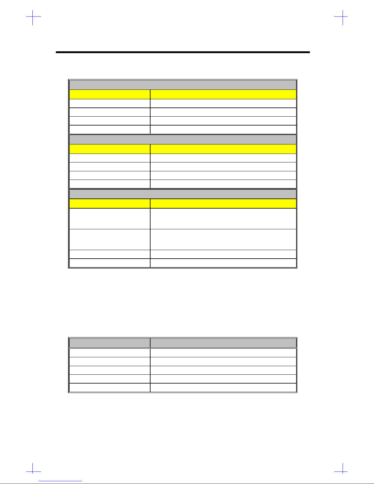
Table 3-1 lists the drive control settings and their corresponding functions.
Page 45
3-14 Service Guide
Table 3-1 Drive Control Settings
Diskette Drive
Setting Description
Normal Diskette drive functions normally
Write Protect All Sectors Disables the write function on all sectors
Write Protect Boot Sector Disables the write function only on the boot sector
Disabled Disables all diskette functions
Hard Disk Drive
Setting Description
Normal Hard disk drive functions normally
Write Protect All Sectors Disables the write function on all sectors
Write Protect Boot Sector Disables the write function only on the boot sector
Disabled Disables all hard disk functions
System Boot Drive
Setting Description
Drive A then C The system checks drive A first. If there is a diskette in the
drive, the system boots from drive A. Otherwise, it boots
from drive C.
Drive C then A The system checks drive C first. If there is a hard disk
(drive C) installed, the system boots from drive C.
Otherwise, it boots from drive A.
C: The system always boots from drive C.
A: The system always boots from drive A.
3.6.2 Onboard Communication Ports
Serial Port 1 Base Address
This parameter allows you to set serial port 1 logical base address.
Table 3-2 Serial Port 1 Settings
Setting Description
3F8h Serial port 1 with address 3F8h using IRQ4
2F8h Serial port 1 with address 2F8h using IRQ3
3E8h Serial port 1 with address 3E8h using IRQ4
2E8h Serial port 1 with address 2E8h using IRQ3
Disabled Disables serial port 1
Page 46
BIOS Setup Information 3-15
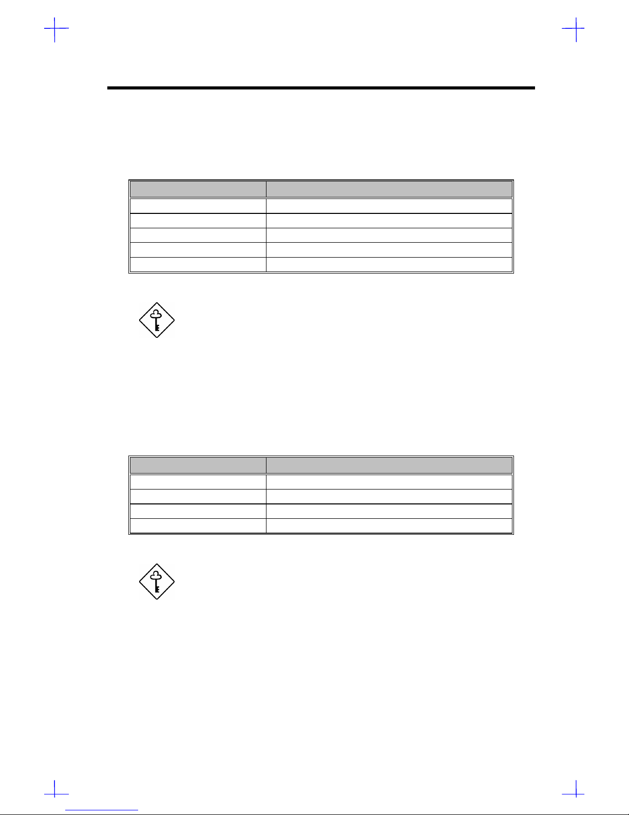
Serial Port 2 Base Address
This parameter allows you to set serial port 2 logical base address.
Table 3-3 Serial Port 2 Settings
Setting Description
3F8h Serial port 2 with address 3F8h using IRQ4
2F8h Serial port 2 with address 2F8h using IRQ3
3E8h Serial port 2 with address 3E8h using IRQ4
2E8h Serial port 2 with address 2E8h using IRQ3
Disabled Disables serial port 2
If you assign 3F8h to serial port 1, you can only assign 2F8h or
2E8h to serial port 2.
If you assign 2F8h to serial port 1, you can only assign 3F8h or
3E8h to serial port 2.
Parallel Port Base Address
The system has one parallel port. Table 3-4 lists the options for selecting the parallel port address.
You also have the option to disable the parallel port.
Table 3-4 Parallel Port Settings
Setting Function
3BCh (IRQ 7) Corresponds to the parallel port with address 3BCh
378h (IRQ 7) Corresponds to the parallel port with address 378h
278h (IRQ 5) Corresponds to the parallel port with address 278h
Disabled Disables the parallel port
The 3BCh (IRQ 7) setting works only with Standard Parallel Port
(SPP) and Standard and Bidirectional operation modes.
To deactivate the parallel port, select the Disabled option. If you install an add-on card with a
parallel port whose address conflicts with the onboard parallel port, the system automatically
disables the onboard functions.
Check the parallel port address on the add-on card and change the address to one that does not
conflict.
Page 47
3-16 Service Guide
OPERATION MODE
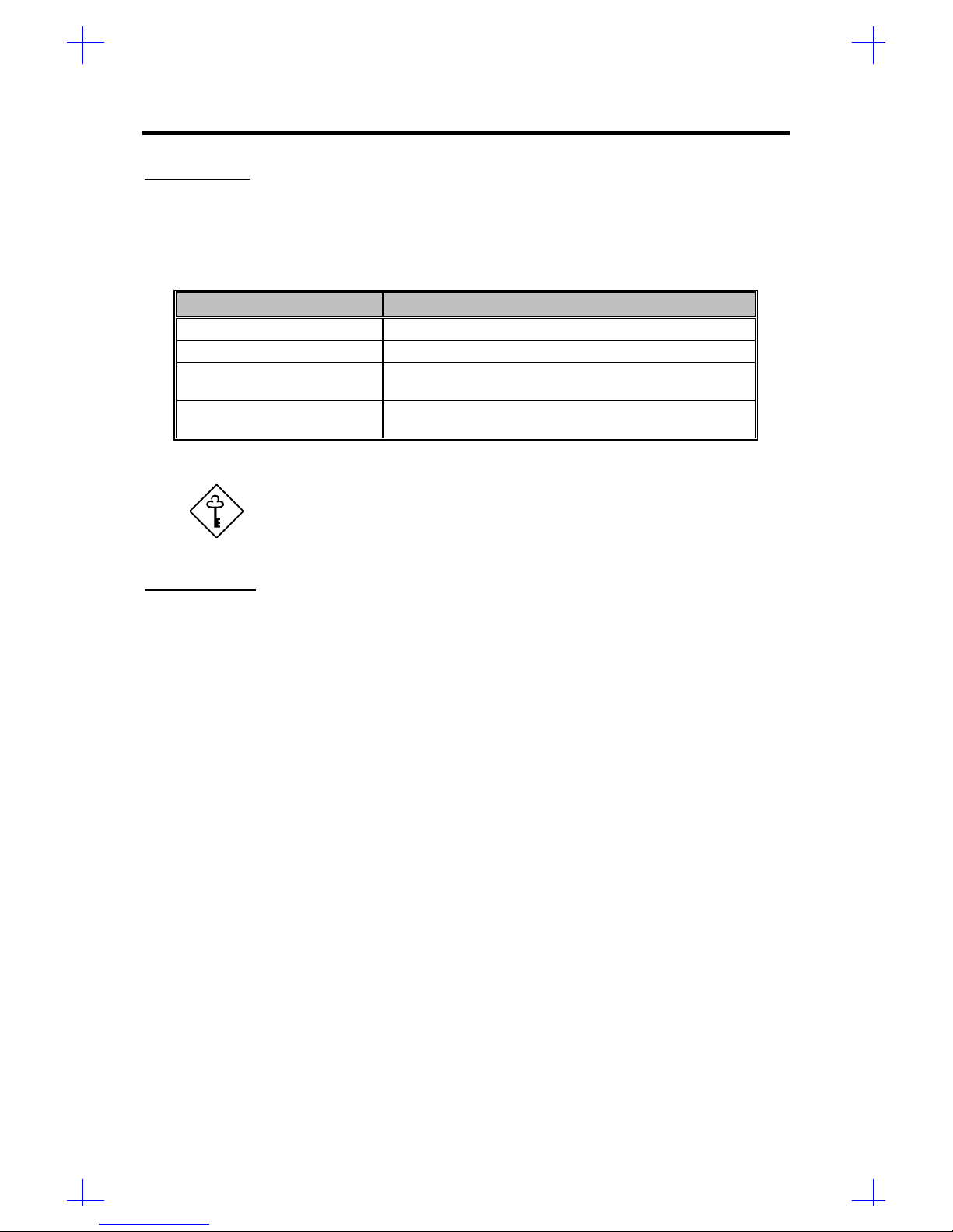
This item allows you to set the operation mode of the parallel port. Table 3-5 lists the available
operation modes of the parallel port.
Table 3-5 Parallel Port Operation Mode Settings
Setting Function
Standard Parallel Port (SPP) Allows normal speed one-way operation
Standard and Bidirectional Allows normal speed operation in a two-way mode
Enhanced Parallel Port (EPP) Allows bidirectional parallel port operation at maximum
speed
Extended Capabilities Port
(ECP)
Allows parallel port to operate in bidirectional mode and at
a speed higher than the maximum data transfer rate
When you select the Enhanced Parallel Port (EPP) or Extended
Capabilities Port (ECP) as operation mode, the parallel port base
address 3BCh (IRQ 7) is not available.
ECP DMA CHANNEL
This item becomes active only if you selected Extended Capabilities Port (ECP) as the
operation mode. It allows you to select DMA channel 1 or DMA channel 3 (as required in
Windows95).
3.6.3 Onboard PS/2 Mouse (IRQ 12)
This parameter enables or disables the PS/2 mouse. When set to Enabled, it allows you to use
the onboard PS/2 mouse assigned with IRQ12. When set to Disabled, it deactivates the mouse
and frees IRQ12 for the use of other devices.
Page 48
BIOS Setup Information 3-17
3.6.4 Setup Password
The Setup password prevents unauthorized access to the BIOS Utility.
Set jumper JP1 on the system board to pins 1-2 to enable the
password function.
Setting a Password
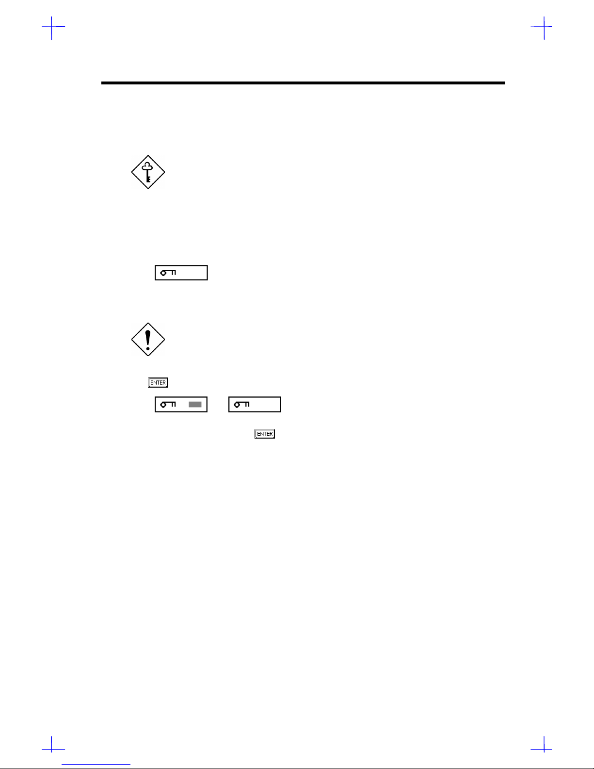
1. Highlight the Setup Password parameter and press the left- or right-arrow key. The password
prompt appears:
2. Type a password. The password may consist of up to seven characters.
Exercise caution when typing your password because the
characters do not appear on the screen.
3. Press . A prompt asks you to retype the password to verify your first entry.
4. Retype the password then press .
After setting the password, the system automatically sets the Setup Password parameter to
Present. The next time you want to enter the BIOS utility, you must key-in your Setup password.
If You Forget the Password
If you forget your password, you must reset the configuration values stored in CMOS to their
default values. Should this happen, call your dealer for assistance.
3.6.5 Power On Password
The power-on password secures your system against unauthorized use. Once you set this
password, you have to type it whenever you boot the system. To set this password, follow the
same procedure as in setting a Setup password.
Page 49

3-18 Service Guide
3.7 Remote Diagnostic Configuration
The Remote Diagnostic Configuration parameters allow you to configure the system power
management feature.
The following screen shows the Remote Diagnostic Configuration parameters and their default
settings:
Remote Diagnostic Configuration Page 1/2
RDM Mode Number .................... [ 5 ]
↑↓ = Move Highlight Bar, → ← = Change Setting
PgDn/PgUp = Move Screen, F1 = Help, Esc = Exit
Remote Diagnostic Configuration Page 2/2
RDM System Critical Paging No. ..... [0 ]
RDM Remote Connection Phone No. .... [0 ]
RDM Remote Connection Password ..... [0 ]
↑↓ = Move Highlight Bar, → ← = Change Setting
PgDn/PgUp = Move Screen, F1 = Help, Esc = Exit
Page 50

BIOS Setup Information 3-19
3.7.1 RDM Mode Number
This parameter allows you to set the RDM notification procedure. The notification options are
listed in the following table:
Table 3-6 Notification Options
Option Notification Procedure
Mode 1 1. Waiting for station call
2. Station dial in
3. Server reboot
Mode 2 1. Server paging
2. Waiting for station call
3. Station dial in
4. Server reboot
Mode 3 1. Server paging
Mode 4 1. Server paging
2. Server auto-reboot
Mode 5 1. Server paging
2. Server reboot
3. Server dial out to station
Disabled Disables RDM function
The default setting is 1.
Mode 1
Mode 1 requires manual station notification. This indicates that once RDM is activated and the
RDM LED turns on1 the server administrator must call the RDM station to notify the service
engineer about the server status. Once the service engineer at the RDM station site is informed
and confirmed the server status, he must run the RDM-station software in order to establish
communication with the RDM agent.
After executing the RDM-station software, the RDM-station application window appears on screen.
Under the Settings option, the service engineer must enter the correct server phone number,
station phone number, and RDM password. The entered password must be the same as the one
specified in the RDM remote connection password BIOS parameter. Otherwise, remote
connection cannot be established. Refer to the RDM User’s Guide for more details on the
RDM-station application.
If remote connection is successfully established, the server automatically reboots. After reboot, it
automatically enters the BIOS utility and allows the RDM station to check and reconfigure the
server BIOS settings, if necessary. After making your modification, reboot the server.
1
A lighted RDM LED indicates either of the following:
a. RDM button is pressed
b. RDM driver has detected server failure.
For more details on activating RDM, see section 3.3.
Page 51

3-20 Service Guide
Mode 2
Once RDM is activated, the RDM module contacts the pager number specified in the RDM system
critical paging number parameter. Once the server engineer received the notification, he must run
the station software to establish communication with the RDM agent.
When connection is established, the station undergoes the same process as in Mode 1 wherein
RDM module requires a password and the remote station phone number to establish the RDM
connection.
Mode 3
Mode 3 is also called as the debug mode. When the server fails or hangs, the RDM module
contacts the pager number specified in the RDM system critical paging number parameter. After
the pager notification, the RDM module automatically isolates the RDM agent and deactivates the
RDM program to prevent the station from accessing the server. This means that you cannot
reboot the server unless you are at the RDM agent site and have direct access to the system.
This mode requires direct server access.
In this mode, notice that the RDM LED is OFF. This indicates that
the RDM function is deactivated.
We recommend you NOT to select this setting unless you want to
disregard the RDM function.
Mode 4
In this mode, when RDM is activated due to server failure, the RDM module contacts the pager
number specified in the RDM system critical paging number parameter and automatically reboots
the server without asking for a password or the remote station phone number. After rebooting, the
server enters normal mode.
This option allows you to minimize the system downtime.
Mode 5
Once the server fails or hangs, the RDM module contacts the specified pager number, reboots the
server, then connects to the RDM station. The RDM station modem must be ON and the system
must be running the RDM-station application in order to establish communication. Otherwise, the
signal sent by the module will not be received by the station at once.
After reboot, the BIOS utility appears on station screen and automatically disconnects the RDMagent keyboard to enable the RDM station function as the main console. This also allows the
station to check and reconfigure the server BIOS settings. After modifying the BIOS settings,
reboot the server.
Page 52

BIOS Setup Information 3-21
In this mode, if the RDM agent fails to establish connection with the
station, it automatically reboots and enters normal mode (same as
in Mode 4).
Disabled
This setting disables the RDM function and puts the system into normal mode. In normal mode,
the system I/O chip allows COM2 port to function as the modem controller. Since the RDM
module deactivates the RDM function, the server is protected from unauthorized and unnecessary
access.
3.7.2 RDM System Critical Paging Number
This parameter allows you to set the pager number that the RDM module must contact once the
server fails or hangs. To enter the pager number, simply highlight the parameter. Type in the
pager number followed by six commas (,). The commas specify the delay. Make sure that you
enter six commas; otherwise, the pager may not receive the complete message.
You may also include the RDM agent modem number or the message that you want to send in the
pager notification. To do this, simply enter the numbers after the comma signs. The valid entries
are 0 to 9 and asterisk (*). Also, these numbers must start and end with the number (#) sign.
To bypass this feature, do not enter any number after the comma signs.
RDM system critical paging no... [905455499,,,,,,#XXXXXXXX#]
Leave the parameter blank to disregard the function.
Pager Number Message
(valid entries: 0-9, * )
(,) Delay
Page 53

3-22 Service Guide
3.7.3 RDM Remote Connection Phone Number
This parameter allows you to set the RDM station number the RDM module must contact once
RDM is activated under the RDM work mode 5 setting. To set, simply highlight the parameter and
enter the station phone number.
RDM remote connection phone number [5455299]
If the remote connection phone number is utilizing PBX line, then you must enter six commas (,)
after the entry phone number followed by the extension number, if any. When entering the
extension number, we recommend that you insert a comma after each number. The commas
specify delay.
RDM remote connection phone number [5455299,,,,,,6,6,4,9]
Leave the parameter blank to disregard the feature.
3.7.4 RDM Remote Connection Password
This parameter prevents unauthorized access of the RDM agent. To set a password, simply
highlight the parameter and enter your code. Your password may contain up to eight characters.
If you specify a password, make sure to take note of it. You will need enter the correct password
before the RDM station gains access to the RDM agent. If you want to bypass the password
feature, leave the parameter blank. When prompted for the password during RDM operation,
press to disregard the prompt.
RDM station number
Delay
Extension Number
Page 54

BIOS Setup Information 3-23
3.8 Load Setup Default Settings
Use this option to load the default settings for the optimized system configuration. When you load
the default settings, some of the parameters are grayed-out with their fixed settings. These grayed
parameters are not user-configurable. If you want to change the settings of these items, disable
the Auto Configuration Mode and the Fast Boot Mode parameters under the Basic System
Configuration menu.
3.9 Leaving Setup
Examine the system configuration values. When you are satisfied that all the values are correct,
write them down. Store the recorded values in a safe place. In the future, if the battery loses
power or the CMOS chip is damaged, you know what values to enter when you rerun Setup.
Press to leave the system configuration setup. If there is any change in the BIOS utility
functions, the following screen appears:
Do you want to save CMOS data?
[Yes] [No]
Select your response with the arrow keys. Select Yes to store the new data in the CMOS. Select
No to retain the old configuration values. Press .
Page 55

3-24 Service Guide
3.10 Hard Disk Types
Type Cylinders Heads Sectors Per Track
None (indicates SCSI or no hard disk)
1 306 4 17
2 615 4 17
3 615 6 17
4 940 8 17
5 940 6 17
6 615 4 17
7 462 8 17
8 733 5 17
9 900 15 17
10 820 3 17
11 855 5 17
12 855 7 17
13 306 8 17
14 733 7 17
15 (reserved)
16 612 4 17
17 977 5 17
18 977 7 17
19 1024 7 17
20 733 5 17
21 733 7 17
22 733 5 17
23 306 4 17
24 612 4 17
25 306 4 17
26 612 4 17
27 698 7 17
28 976 5 17
29 306 4 17
30 611 4 17
31 732 7 17
32 1023 5 17
33 751 8 17
34 755 16 17
35 731 13 26
36 980 15 17
37 936 16 17
38 981 5 17
Page 56

BIOS Setup Information 3-25
Type Cylinders Heads Sectors Per Track
39 981 10 17
40 762 8 39
41 980 5 17
42 832 8 33
43 683 12 38
44 513 16 38
45 776 8 33
46 683 16 38
47 832 6 33
48 615 2 34
49 989 16 63
50 823 4 38
51 1001 15 17
52 1024 17 22
53 723 13 51
54 548 8 38
55 1013 4 41
56 929 15 17
57 817 14 36
58 723 13 81
59 802 4 39
60 1024 9 17
61 895 5 55
62 (reserved)
63 966 10 34
64 1024 8 17
65 1024 11 17
66 918 11 17
67 965 14 49
68 1024 10 17
69 1024 12 17
70 1024 13 17
71 1024 14 17
72 1024 11 50
73 1024 16 17
74 918 15 17
75 1010 16 51
76 1024 5 17
77 1024 8 17
78 (reserved)
Page 57

3-26 Service Guide
Type Cylinders Heads Sectors Per Track
79 1001 15 32
80 1024 16 63
81 1024 7 17
82 988 16 52
83 1024 15 17
84 776 8 33
85 926 13 17
86 805 4 26
87 976 5 17
88 685 16 38
89 1011 15 22
90 997 10 53
91 985 13 32
92 816 15 32
93 968 5 17
94 903 8 46
95 966 5 34
96 535 10 50
97 715 10 50
98 1016 16 63
99 996 16 63
Auto or User (User-defined)
 Loading...