

Bimatek D 1045 VNP Maintenance Manual

DDVVDD LLAASSEERR DDIISSCC PPLLYYEERR
D 1045 VNP
Maintenance Manual
Use the book with instruction. Read the manual and
O/I carefully before maintain the unit
PDF created with pdfFactory Pro trial version www.pdffactory.com

TABLE OF CONTENTS
▲ Safety information ----------------------------3
1. General guide -----------------------------3
2. Low zeta potential leaking inspection ----3
3. High zeta potential leaking inspection ----3
▲ Device avoiding ES(Electric Susceptible)
Influence of ESD (Electric Susceptible
Discharge)----------------------------------------- 4
▲ Technical specification ------------------------4
▲ Mechanical diagram ------------------ --------5
Mechanical Parts ----------------------------6
▲ Packing and accessories ----------------------7
▲ Disassemble and assemble --------------------8
1. Take out disc from trouble player ------8
2. PCB circuit board’s location -------8
▲ Disassemble and assemble parts of the unit -9
1. Can open the tray by electricity --------9
2. Can not open the tray by electricity ----9
3. Assemble the unit ----------------------9
▲ Attachment 1 -------------------------------10
▲ Block Diagram/Electric circuit diagram ---10
1. Block diagram ---------------------------11
2. Decoder board diagram -----------------12
3. AV output board diagram ---------------17
4. Power board diagram -------------------18
5. Control board diagram ----------- ------19
▲ Attachment 2--------------------------------20
▲ PCB Diagram ------------------------------20
1. Upper decode board PCB diagram ----21
2. Lower decoder board PCB diagram --22
3. AV output board PCB diagram -------24
4. Power board PCB diagram ------26
5. Control board PCB diagram -----28
▲ Attachment 3---------------------------------30
▲ Component list-------------------------------30
1. Power board component list ------------------31
2. Decoder board component list ----------------33
3. AV output board component list --------------37
4. Control board component list -----------------38
2
PDF created with pdfFactory Pro trial version www.pdffactory.com
SAFETY INFORMATION
General guide
1.Observe the original circuit during maintenance. if short
circuit occurs, change the over-hot or damaged components.
2.Observe all the protective device after maintenance, such
as whether the shielding cover or paper is assembled well.
3.To avoid electric shock, please inspect electricity leakage
after maintenance
Low zeta potential leaking inspection
1.Take out AC cord and connect a piece of wire between two
legs of the outlet.
2.Use Gear R x 10K of the voltmeter to measure the spares
on AC outlet and exposed metallic part with short circuit.
The resistance between screw cap, control shaft should be
unlimited.
Ω
uF
AC voltage table
to have discover metal
accessory of equipment
creepage checking circuit
cold water
canal (earthing )
picture 1
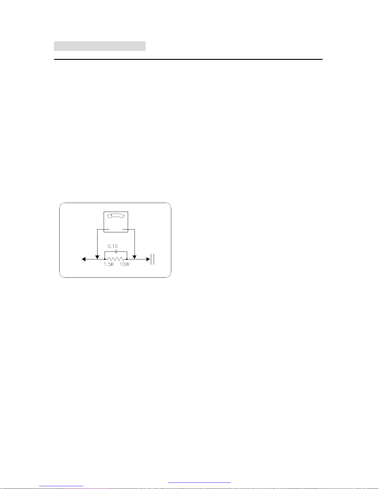
High zeta potential leakage inspection
.As illustrated 1, Connect Resistor with 1.5K, 10W and
capacitor 0.15 between exposed metallic part and device of
fine connection to the earth (water pipe etc.).
2.Plug-in AC cord directly to AC outlet. Do not inspect with
shield adaptor.
3.Utilize 1000 or more sensitive voltmeter to measure
alternating voltage.
4.Turn back the AC plug-in from AC outlet then iterate the
inspection as above.
5.Inspect the voltage of the resistor between other exposed
metallic parts and the earth with the same way.
6. The voltage must not be over than 0.75Vrms at any points
on the resistor. Electric leakage should not be over 0.5mA
when processing high voltage leakage testing through
Device avoiding ES(Electric Susceptible)
Influence of ESD (Electric Susceptible Discharge
exceeded the restrained figure, electric shock should be
possibly suffered. Do maintain the unit and inspect once
more before return to the user.
Device avoiding ES influence of ESD.
Some solid semi-conductor devices are easy to be
damaged by static electricity. These devices are generally
called ES device. The typical devices are IC, field effect
component and semi-conductor laser diode.
The following technology helps to abate the danger of
ESD on body before handle any semi-conductor or
semi-conductor component. Or wear the ESD bangle availed
from the market to eliminate the threaten of static electricity
on human body.
2.Put the electronic parts with ES device on the surface of
conductor such as aluminum foil after take them out in order
to protect static electricity from accumulation and explosion.
3.Solder or disassemble ES device through iron connecting
the earth.
4. Utilize device only anti-static electricity to disassemble
soldering tin. Non-anti static electricity device (ESC
protection) will release ES that damage ES device.
5.Do not use chemical volatile releasing static electricity
that leads to damage ES device
6. Unless preparation for pre-assembling has been made, do
not take out the ES device to be changed from the protective
packing ( most of the changed ES devices are packed
together with anti-static electrical foam or similar electric
material, besides, countermeasures for down-lead short
circuit are taken.).
7. Protective material should connect the model or the circuit
component to be assembled in it before taking out the
protective material from the ES device.
Note: do not bear electricity to the model or the circuit, and
pay attention to all the other safety information.
8. When disassembling and replacing the ES device, try to
reduce body movement (Or, the movement of legs, the
friction of fibrous of clothes, or elevating the legs from the
floor will generate static electricity ESD, causing damage to
the ES device.).
3
PDF created with pdfFactory Pro trial version www.pdffactory.com
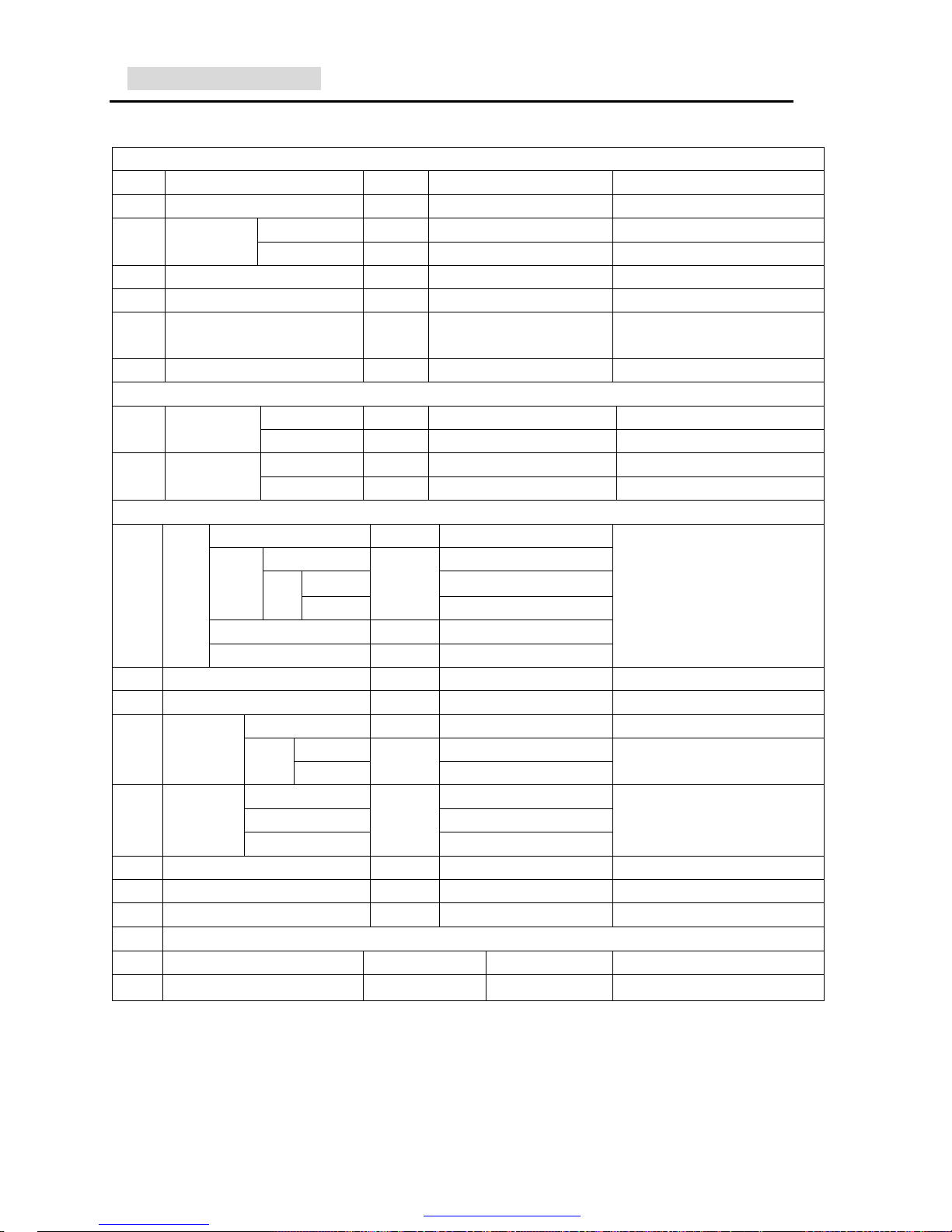
Technical specification
A Audio parts(front R. L channel output)
NO. ITEMS UNITS LIMITED TEST CONDITION
1
Level output(1KHz,0dB)
Vrms 1.8+0.2/-0.8
DVD(LPCM)、 CD
Fs=48KHz dB
±1
DVD(LPCM) 20Hz~20KHz
2
Frequency
Range CD dB
±1
CD 20Hz~20KHz
3
Distortion + Noise(1KHz,0dB)
dB
≤-65
CD DVD(LPCM) A power
4
S/N Ratio : (S/N)
dB
≥90
CD A account power
5
Path Separation
dB
≥80
DVD(LPCM)、CD 、R—L、A account
power
6
Channel Imbalance
dB
≤1.5 DVD(LPCM)、CD
B Digital audio parts
range Vp-p
0.5±20% 75W± 1% loads
1 Coaxial output
impedance
W 75± 30%
wavelengh(λp)
nm
660±30
2 Optical output
power(Pc) dBm
-27≤Pc≤-18
C Video parts
video Vp-p
1.0±0.2
Y
0.700±0.140
chroma
0.880±0.176
S-video
C
In-phase
Vp-p
0.300±0.060
Y. CR. CB Vp-p
0.700±0.140
1
Outpu
t
range
R G B
0.700±0.140
Loads 75W± 1%
2 Level exculpate rate lines
≥500
3
bandwidth(+3/-6dB 时)
MHz
≥5.5
100KHz 0 dB
Y dB
≥56 (account power)
75W loads
U channel
≥50
4 S/N
C
V channel
dB
≥50
75W loads
R channel
≥50
G channel
≥50
5
R、G、B
S/N Ratio
B channel
dB
≥50
75W loads
6
Differential coefficient gain (DG)
%
≤2
75W loads
7
Differential coefficient bit (DP)
degree
≤2
75W loads
8
Lum blame non line of distortion
%
≤5
75W loads
D Power
1 Input power voltage
~90/240V
60Hz/50Hz
2
Power Consumption
≤15 W
Normal works
NOTE:DVD test type:TVD-540A CD test type:TCD-784
4
PDF created with pdfFactory Pro trial version www.pdffactory.com

Mechanic parts of decompose diagram
5
2
1
3
27
17
17
27
5
4
27
27
12
29
6
11
27
8
10
28
29
15
32
32
26
29
16
32
17
32
17
21
32
32
14
28
7
15
31
9
13
28
31
31
20
19
32
28
33
22
33
33
28
28
31
31
31
17
17
31
17
31
17
25
32
32
32
18
32
23
33
PDF created with pdfFactory Pro trial version www.pdffactory.com
ABSY1-2101I1-00
power button
7
8
ST3X
ST3X8PWTTNiH
roundhead triangle tooth supply plating nickel
(over forcedly)plating nickel
N2-300612-54
N2-300614-54
N2-301215-54
32
33
31
ST3X12PWTTNiH
plating nickel
S-video、motherboard and rear board
decode board,power board,motherboard
upper cover and motherboard
7
4
1
VGA lines(6P/2.0mm pin+15P VGA jack)
WQ-201066-10
19
triangle tooth supply plating nickel
L4-150250-30
magnetic annulusT25X15X12mm
25
28
N2-300612-19
N2-300815-54
N2-300812-19
29
30
N2-300614-54
WD-651202-00
27
26
ST3X8PANi
plating nickel
KTT3X
ST3X6PANi
plating nickel
power cord length320mm VDE attestation
(sinking) plating nickel
power cord 2.5M 250V6A VDE attestation
Q2-250201-10
22
WD-252232-00
24
23
A5-200100-20
A5-250300-10
21
20
decode board
rear board
AV board
1
power switchs,upper cover panel,rear board
13
control board and panel board
chips and motherboard
6
4
surface and motherboard
1
5
1
1
1
1
power switchs PS4E-A-040(VDE attestation)
16
Y3-030260-20
A6-898000-40
18
17
Y3-017003-10
A5-250200-30
Q4-250201-00
15
14
KDA-898SP SANYO chips
PCB stanchion
feet mat
switchs power board
motherboard
Y1-250111-00
Q3-200100-00
A5-250200-40
12
13
11
S1-404000-00
Y1-250151-00
Y3-180160-10
9
10
8
key combination
upper cover
control board
buttons
upper cover plank
1
electrolyse board
1
1
9
2
1
electrolyse board
1
ABS
ABS
cool roll board
N4-060201-L0
3
N4-060201-R0
Y9-250120-30
Q1-250103-10
5
6
4
Q1-2501E3-10
Y9-250121-30
2
Serial No.
Material No.
tray spring(left)
big lens
surface
tray spring(right)
Name
lens
DVD tray
MECHAINC PARTS OF COMPONENT LIST
1
carbon wire
carbon wire
ABS
QTY
ABS
REMARK
6
PDF created with pdfFactory Pro trial version www.pdffactory.com
O5-250201-10
O7-250101-R0
A1-310100-10
O1-500600-10
O7-250101-L0
O6-250101-00
Part No.
1
4
5
6
3
2
2.Material List
Serial No.
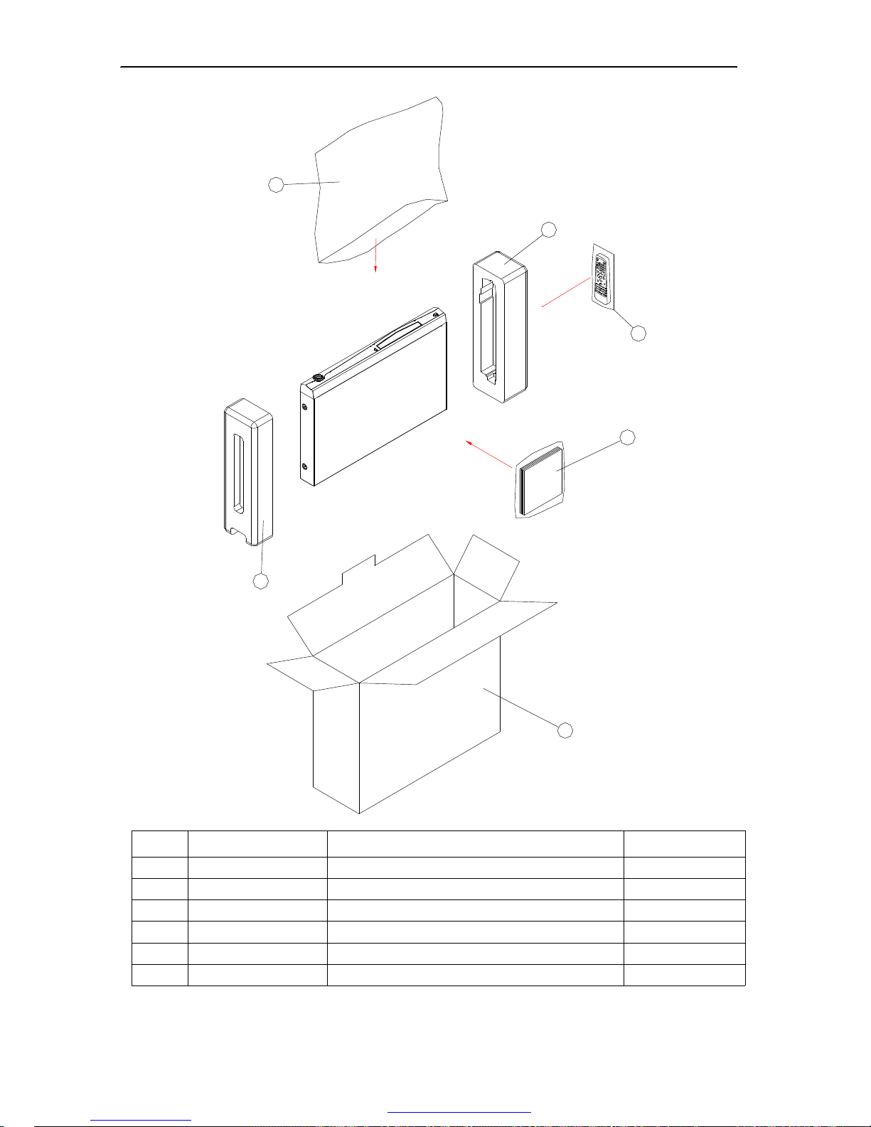
PACKING AND ACCESSORY
1.Decompose diagram
color box
remote control
froth glue(right)
instruction booklet
froth glue(left)
machine bags 500*600mm
Descrption and Specification
1
1
1
1
1
1
QTY
1
2
6
4
3
5
7
PDF created with pdfFactory Pro trial version www.pdffactory.com
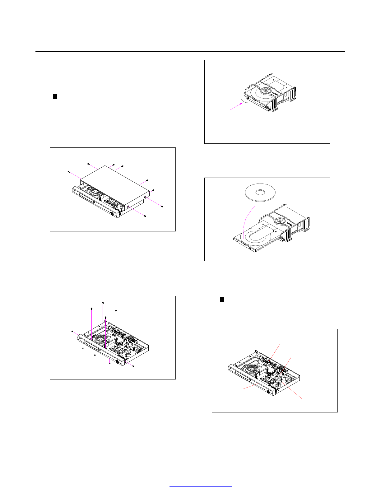
Diagram C Rotate white gear
3.Take out front panel and loaderd carefully,there is a white
plastic gear under the loader,Rotate the rear as diagram C to
stretch DVD tray and door(diagram D),you can take disc out
carefully.
Diagram B Panel,chip disassemble
Diagram H boards Location
Control board
decode power board
2.Wring 3 screws out connected base panel with bottom
board then wrest 4 screws connected loader ewith bottom
board (Diagram B)
Diagram D Take out disc
decode board
AV output board
Per PCB assemblies locate as(see diagram H)
PCB position
Diagram A Dipart cabinet
Take out disc of method from a trouble machine
If you cannot take out disc even press OPEN/CLOSE
button,please pull power cord from the socket and
follow as below:
1.Wring 8 screws out then pull left and right side
to take away top panel that rear part of upper
(Diagram A)
The unit comprises mechanical and electric part,including:
front panel,base panel,top panel,rear panel and loader,AV
output board,decode board,etc.
DISASSEMBLE AND ASSEMBLE
White Gear
8
PDF created with pdfFactory Pro trial version www.pdffactory.com
Assemble the unit
Assemble the case by reversing disassembly
After maintenance, switching on power on the
condition that assembly and connection have
no mistake then loader and electric circuit return
to original place automatically .The unit works normally.
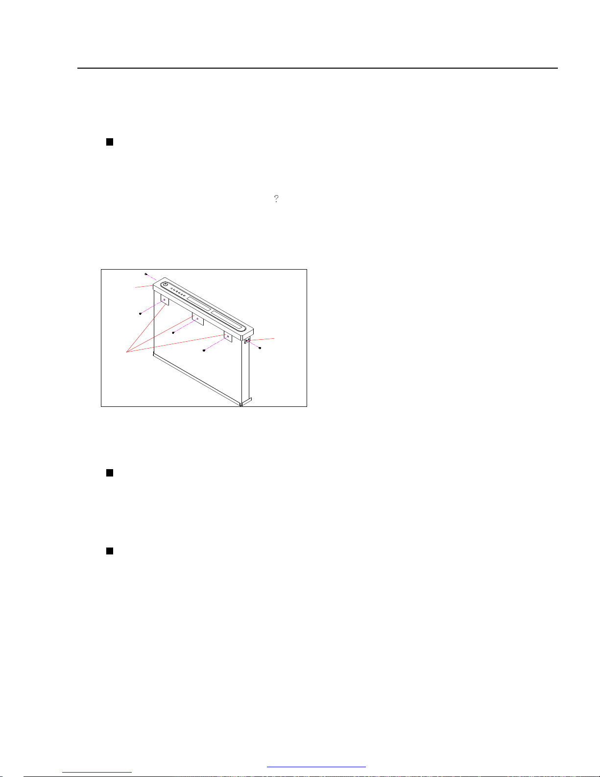
Can not open tray by electricity
Unable to open disc tray when press OPEN/CLOSE button
1. Take down disc as illustrated A,B,C,D
2. Take down DVD front panel
Can open the tray by electricity
1. Operate after completely take out top panel
2. Press OPEN/CLOSE button to open disc tray.
Be careful not to damage disc when take it out if it is in the tray .
Then take away DVD door (as illustrated E)
Graph E Catch position on the front panel
Catch
Catch
Catch
1. Take down top panel see as illustrate A
2.Take down front panel
Disassemble and assemble parts of the unit
9
PDF created with pdfFactory Pro trial version www.pdffactory.com

Attachment 1:Block diagram、Circuit diagram
Block diagram
Decoder board circuit diagram
AV Output board circuit diagram
Power board circuit diagram
Control board circuit diagram
10
PDF created with pdfFactory Pro trial version www.pdffactory.com
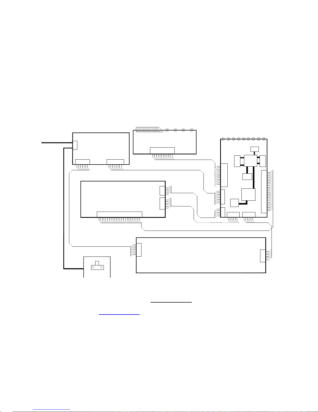
Block diagram
11
RGB-CON
GND
POWER SW
STBY
+5V
NC
F+
F-
GND-PDANCT+T-BVCEF
VCC
-3.3V
-27V
+3.3V
LD-DVD
LD-CD
VR-CD
CD/DVD
LD-CD
VR-DVDDCNCMD
HEM
GND-LD
GND
-27V
-3. 3V
+3.3V
~220V
~220V
CVBS
R/V
79A LOADER
-12 V
STBY
+5V
NC
+5VD
GND
GND
+5VA
+12V
GND
STBY
POWER SUPPLY
SCART
SP+
VR-CD
-12V
SP-
PANEL CONTROL
LIMIT
SL+
GND
SL-
TRIN
GND
LOADLOAD+
TROUT
STBY
CLK
IR
DIN
STB
DOUT
GND
VR-DVD
GND-LD
LD-DVD
LD-CD
CLK
LI MI T
GND
SP+
SL-
SL+
DOUT
GND
BA5954FM
STBIRDIN
HEM
MD
FR
F-SEL
B/U
GND
G/Y
GND
SPDIF
R-IN
+5V
L-I N
LOAD+
SP-
GND
TRIN
TROUT
LOAD-
L-IN
+5VA
+12V
GND
GND
GND
+5VD
+5V
SPDIF
R-IN
GND
G/Y
F-SEL
B/U
GND
CVBS
RGB-CON
R/V
OPTICAL
AV OUT
Pr/CrYPb/Cb
COAXTAL
CD/DVD
LD-CD
GND-PD
T-
FLASH
ZR36707
VCC
NC
D
C
F
A
VC
E
B
NC
ZR36768
SDRAM
F+
T+
F-
SDRAM
S-VIDEO
DECODER
SRSL CEN
PCM1606
SUB FL VIDEO
PDF created with pdfFactory Pro trial version www.pdffactory.com
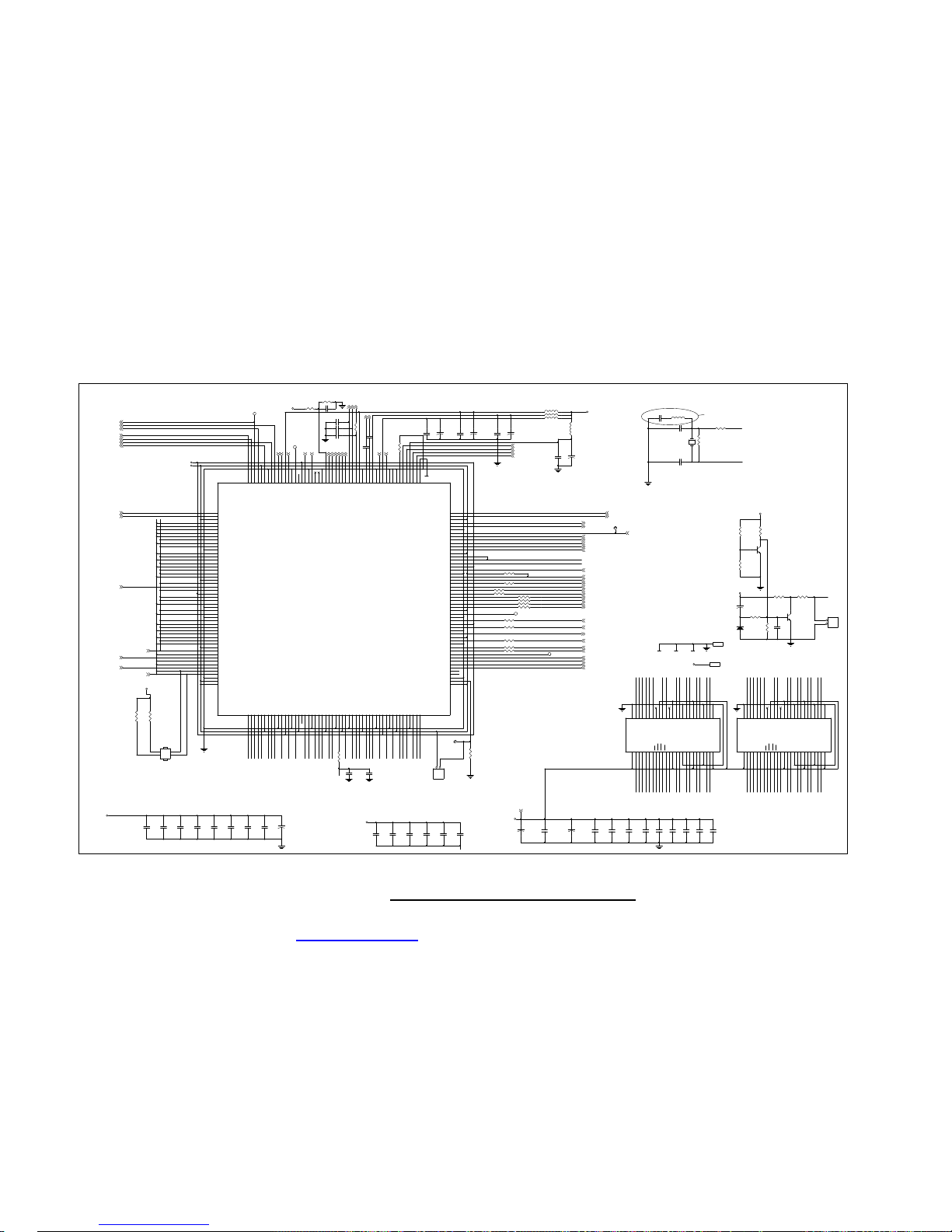
12
Decode board elements diagram
1
MEMWR-
VR_SEL
SPDIF
DUPRD0
RAMA DD7
MEMDA11
R200 0R
R164 392R/1%
RAMADD6
RAMDAT6
R10 33
FB26 FBR
JP24
CN2.54MM2X2-M
341
2
BC6
0.1uF
RAMADD10
RAMDAT11
RAMDAT3
MEMAD11
BC17
0.1uF
BC241 10nF
DSPVCC18
MEMAD15
RD40
10K (NC)
DSPVCC33
DSPVCC33
DEFECT
TRA CK_DA C
VSYNC
DUPTD0
MEMAD10
RAMDAT9
+
C16
100uF/16V
RAMADD2
RAMDQM
RAMDQM
OSCOUT
+
C15
100uF/16V
TP7
1
.
R6 33
BC4
0.1uF
FS2
RAMADD5
MEMAD[20:0]
DRVSB
AAF_TE
RAMCS0-
RAMADD10
MEMCS1-
MEMDA3
PLLCFGP
MEMDA0
INSW
MEMDA10
MEMAD1
BC10
0.1uF
BC243 10nF
+
C128
47uF/16V
BC27
0.1uF
DUPTD0
C105
330P
BC242 10nF
C225 22pF
TP5111
.
BC21
0.1uF
Y_R_V
INSW
RAMDAT3
RAMBA
DSPVCC33
ALRCLK
R15
4.7K
OSCOUT
PCLK
MEMDA12
R190 330R
BC28
0.1uF
RAMADD7
RAMDAT9
12CCLK
LINK
NNN
RAMDAT9
RAMWE-
R22 4.7K
R125 10K
**
220pF
DSPVCC18
C224 22pF
IALRCLK
BC3
0.1uF
DSPVCC33
I2CDAT
RAMDAT2
RAMADD8
RAMDAT0
RAMADD9
BC12
0.1uF
D14
RLS4148 (NC)
FPC_STB
RAMDA T14
RAMDA T12
RAMB A
FPC_STB
AFEGND
AOUT2
AIN
MEMAD19
ICETCK
MEMDA5
R183
100K
RAMDAT1
AOUT1
RAMA DD2
RAMA DD10
RAMB A
BC19
0.1uF
RFA_SDATA
CLOSE
DUPRD1
RAMD AT14
MEMDA9
MEMAD13
MEMAD8
RAMA DD3
BC9
0.1uF
RAMDAT15
SPDIF
RD39
10K (NC)
RAMD AT15
DRVSB
MEMWR-
HOMESW
DSPVCC33
ICETMS
R14
4.7K
BC7
0.1uF
D+5V
MEMCS1-
DUPTD1
AMUTE
MEMCS0-
RAMRAS-
MEMAD4
AOUT2
Q11
SST3904
1
2 3
RAMDAT12
BC25
0.1uF
R127
0R
SPINDLE_PW M
RAMDAT2
TP22
1
.
SPDL_SENS
/AUDIO_RESET
RAM DAT 7
OUTSW
RAMDAT12
RAMRAS -
RAMDQM
RAMADD0
DUPRD1
GPAIO
HSYNC
MEMCS0-
CLOSE
AAF_P I
RAMDAT5
RAMCAS -
RN3 33R X4
12
34
56
78
I2CCLK
RAMDQM
RAMDAT6
Y2 27.000MHz
VGND
RAMA DD0
FB4 FBR
PLAY MODE:ALL OPEN
C104
330P
BC1
0.1uF
BC14
0.1uF
DSPVCC33
MEMAD12
C_B_U
ABCLK
OUTSW
RAMDAT7
RAMDQM
RAMADD5
RAMDAT3
RAMDAT1
MEMAD20
IABCLK
R239
150
STANDBY
MIRR
PCLK
RAMD AT4
LDON
AAF_C E
RAMDA T6
ICETDO
R161 33
FB2 FBR
U15
ZR36768
12
1
2
3
4
5
6
7
8
9
10
11
50
13
14
15
16
17
18
19
20
21
22
23
24
25
26
27
28
29
30
31
32
33
34
35
36
37
38
51
52
535455625657585960
617263646566676869707183737475767778798081
829184858687888990
1019293949596979899
100
102
103
104
105
156
155
154
152
151
145
136
144
143
142
141
140
139
138
127
125
124
123
122
121
120
119
118
117
116
115
114
113
112
111
110
205
204
202
192
190
200
187
195
197
186
185
184
175
174
173
172
171
157
169
160
167
165
164
163
162
161
159
158
39
40
41
42
43
44
45
46
47
48
49
106
107
108
109
126
128
129
130
131
132
133
134
135
137
146
147
148
149
150
153
166
168
170
183
182
181
180
179
178
177
176
188
189
191
193
194
196
198
199
201
203
206
207
208
GNDP
SSCRXD/GPCIO[17]
MEMCS[1]#/GPCIO[18]
VDDP
MEMAD[15]/PLLPROG[0]
MEMAD[16]/PLLPROG[1]
MEMAD[14]/PLLPROG[2]
MEMAD[13]/AFETESTEN
MEMAD[12]/[PLLCFGA]
MEMDA[15]
MEMAD[11]/[PLLCFGP]
MEMDA[7]
GNDP
MEMAD[10]/[TESTMODE]
MEMDA[14]
MEMAD[9]
MEMDA[6]
MEMAD[8]
MEMDA[13]
MEMDA[5]
MEMAD[20]/[GPCIO19]/[MEMCS#2]
VDDP
MEMDA[12]
MEMWR#
MEMDA[4]
VDDC
MEMDA[11]
MEMDA[3]
MEMAD[19]/[PLLSEL]
GNDC
MEMDA[10]
MEMAD[18]
GNDP
MEMDA[2]
MEMAD[17]
MEMDA[9]
MEMAD[7]
MEMDA[1]
MEMAD[6]
VDD-IP
VDDP
RAMA DD[4 ]
RAMA DD[3 ]
RAMA DD[5 ]
GNDP
RAMA DD[2 ]
RAMA DD[6 ]
VDDP
RAMA DD[1 ]
RAMA DD[7 ]
RAMA DD[0 ]
GNDP
RAMA DD[8 ]
VDDC
RAMA DD[1 0]
GNDC
RAMA DD[9 ]
VDDP
RAMA DD[1 1]
RAMC S[0] #/RA MBA[ 1]
RAMB A[0 ]
GNDP
RAMC S[1] #
RAMR AS#
RAMC AS#
VDDP
RAMW E#
RAMD QM
GNDP CLK
PCLK
VDDP CLK
RAMD AT[8 ]
GNDP
RAMD AT[7 ]
RAMD AT[9 ]
RAMD AT[6 ]
VDDP
RAMD AT[1 0]
RAMD AT[5 ]
RAMD AT[1 1]
GNDP
RAMD AT[4 ]
VDDC
RAMD AT[1 2]
GNDC
RAMD AT[3 ]
VDDP
RAMD AT[1 3]
RAMD AT[2 ]
RAMD AT[1 4]
RAMD AT[1 ]
RAMD AT[1 5]
RAMD AT[0 ]
VDDP
DUPTD1/GPCIO38
DUPRD1/GPCIO37
VDD-IP
DUPRD0/GPCIO35
GNDP
GPCI/O[32]
GPCI/O[31]
VDDP
GCLKA
GCLKP
XO
VDDA
RESET#
GNDA
VDDP
GNDP
HSYNC/GPCIO25/[CJTDO]
VDDC
VSYNC/GPCIO24/[CJTDI]
GNDC
AIN/[GPCIO23/CJTCK]
VDDP-A2
AMCLK
GNDP-A2
ABCLK
ALRCLK
GPAIO/[AOUT3]
AOUT[0]
AOUT[1]/[GPCIO22]
AOUT[2]/[GPCIO21]
SPDIF
SLE DPU LSE /IDG PCIO 6
VDD P
GNDP
VDD C
GNDC
DEF ECT /IDG PCIO 5
PWM ACT [0]/G PCI O39
GNDP WM
VDD PWM
GNDA FE S
VBI ASS 1
VBI ASS 0
VDD AFE S
GNDA FE RF
RFIN N
RFIN P
VDD AFE RF
GNDD ACD
DAC DRIV E[1]
VDD DAC
DAC DRIV E[0]
GNDD ACB S2
GNDD ACP
RSE T
C/B /U
Y/R /V/[ C]
CVB S/C /[Y]
CVB S/G /Y
MEMDA[8]
MEMAD[5]
VDDP
MEMDA[0]
MEMAD[4]
MEMRD#
MEMAD[3]
MEMAD[2]
MEMCS[0]#
MEMAD[1]/[BOOTSEL2]
MEMAD[0]/[A]PLLSEL/[BOOTSEL1]
CPUNMI/GPCIO[20]
GNDP
[A]GPCIO110/BOOTSEL1/[AOUT3/ICGPCIO0]
[A]GPCIO111/BOOTSEL2/[IDGPCIO0]
COSYNC/GPCIO120/[ICGPCIO1/CJTMS]
GPCIO26/ICETMS/[DJTMS]
ICETDI/GPCIO122/[ICGPCIO2/DJTDI]
ICETDO/GPCIO123/[IDGPCIO1/DJTDO]
ICETCK/GPCIO27/[DJTCK]
GPCIO28/DJTMS
GPCIO29/DJTDI
GPCIO30/DJTDO
GPCIO128/DJTCK/[ICGPCIO3]
GPCI/O[130]/[IDGPCIO2]
GPCI/O[135]/[ICGPCIO4]
GPCI/O[33]
GPCI/O[137]/[ICGPCIO5]
GPCI/O[34]
GPCI/O[139]/[IDGPCIO3]
DUPTD0/GPCIO36
GNDDACPS
VDDDACS
GNDDACDS
ADCIN0
ADCIN1
ADCIN2
ADCIN3
ADCIN4
ADCIN5
ADCIN6
ADCIN7
PWMACT[1]/GP CIO40
PWMCO[0]/GPC IO41
PWMCO[1]/GPC IO42
PWMCO[2]/GPC IO43
PWMCO[3]/GPC IO44
PWMCO[4]/GPC IO45
PWMCO[5]/GPC IO46
PWMCO[6]/GPC IO152/[IDGPCIO4]
ICGPCIO6
GPCIO159/[ICGPC IO7]
SPINDLEDPU LSE/IDGPCIO7
SSCCLK/GP CIO47
SSCTXD/GP CIO16
PLLCFGA OPEN
R22 7 4.7K
R162 33
JP23
1
2
OSCIN
RAMC S1-
RAMA DD9
DUPTD1
RAMD AT13
CJTDO
R228 33
IRRCV
12CDAT
RAMADD1
MEMDA6
U1
K4S161622C-TC/L70
12345678910111213141516171819202122232425
50494847464544434241403938373635343332313029282726
VDD
DQ0
DQ1
VSSQ
DQ2
DQ3
VDDQ
DQ4
DQ5
VSSQ
DQ6
DQ7
VDDQ
LDQMWECAS
RASCSBA
A10/APA0A1A2A3
VDD
VSS
DQ15
DQ14
VSSQ
DQ13
DQ12
VDDQ
DQ11
DQ10
VSSQ
DQ9
DQ8
VDDQ
NC
UDQM
CLK
CKE
NC
A9A8A7A6A5
A4
VSS
AOUT1
**
2.7uH
BC46
15P(NC)
+3.3V
RAMDAT11
RAMADD3
IAMCLK
RF33V
RFA_SDEN
MEMAD2
BC33
0.1uF
TP3
1
.
RFI NP
MNT R
MEMAD5
MEMAD17
R12
4.7k
R126 5.1K
DOWNLOAD MODE:SHORT1-3&2-4
PCLK
RAMRAS-
BC18
0.1uF
BC24
0.1uF
RAMADD4
R250 75
C100
0.1uF
FPC_DOUT
CVBS_G_Y
STANDBY
BC13
0.1uF
D+5V
RESET-
RAMDA T8
BC2
0.1uF
RAMCAS-
RAMADD4
VGND
RAMD AT1
RAMD AT0
R79 0
not install
SLED_PW M
/AUDIO_RESET
AIN
MEMDA13
BC15
0.1uF
RAMADD2
LDON
RAMAD D1
RAMDA T5
BC26
0.1uF
+
C127
47uF/16V
RAMCS0-
ICETDI
BC20
0.1uF
Q12
SST3904
1
2 3
U3
K4S161622C-TC/L70
12345678910111213141516171819202122232425
50494847464544434241403938373635343332313029282726
VDD
DQ0
DQ1
VSSQ
DQ2
DQ3
VDDQ
DQ4
DQ5
VSSQ
DQ6
DQ7
VDDQ
LDQMWECAS
RASCSBA
A10/APA0A1A2A3
VDD
VSS
DQ15
DQ14
VSSQ
DQ13
DQ12
VDDQ
DQ11
DQ10
VSSQ
DQ9
DQ8
VDDQ
NC
UDQM
CLK
CKE
NC
A9A8A7A6A5
A4
VSS
MEMRD-
OPEN
VR
RAM ADD 4
IRRCV
RAMA DD9
RAMD AT4
MEMDA1
FB3
FBR
CJTCK
RAMA DD6
BC11
0.1uF
SDRAM speed <=7ns
FOCUS_DAC
AMCLK
DUPRD0
RAMD AT14
TP11
.
JP22
CN2.54MM2P-M(NMI button)
1
2
DEFECT
RAMD AT5
CJTDI
RAMD AT7
R20
4.7k
RESET-
MEMAD9
MEMAD0
C101
0.22uF (NC)
MEMDA15
RAMADD0
RAMDAT15
MEMAD14
+
C17
100uF/16V
HOMESW
AAF_FE
DEM
OSCIN
RAMA DD1
MEMDA7
RAMDAT10
BC45
15P(NC)
RAMD AT4
RAMD AT2
MEMDA2
RAMCS1-
GND
SGND
MIRR
RAMD AT10
RAMD AT11
AOUT0
MIC_DET
RAM ADD 6
RAM DAT 8
BC30
0.1uF
MEMDA14
MEMAD3
RAMD AT13
IPCL K
MEMRD-
DSPVCC33
MEMDA[15:0]
VR1
RAMADD7
RFINN
HSYNC
DSPVCC18
RESET-
BC8
0.1uF
RAMDAT8
RAMADD3
MEMAD6
+
C14
100uF/16V
CVBS_C
VSYNC
RAMC AS-
MEMAD16
MEMAD18
FPC_CLK
FPC_CLK
DSPVCC33
R9 33
C24
10u/16V (NC)
TP4
1
.
+
C4
47uF/16V
RAMWE-
MEMDA8
FPC_DOUT
RAMA DD8
RAMD AT10
RAMW E-
RFA _SCLK
FS1
AOUT0
RAMA DD5
MEMDA4
R234 33
R19
2k
RAMADD8
RAMDAT13
RAMDAT0
CJTMS
MEMAD7
BC5
0.1uF
BC29
0.1uF
Use pin 128#,130#,131# of I64 to output AMUTE
FS2 and DEM controL signal.
PDF created with pdfFactory Pro trial version www.pdffactory.com
 Loading...