

Page 1
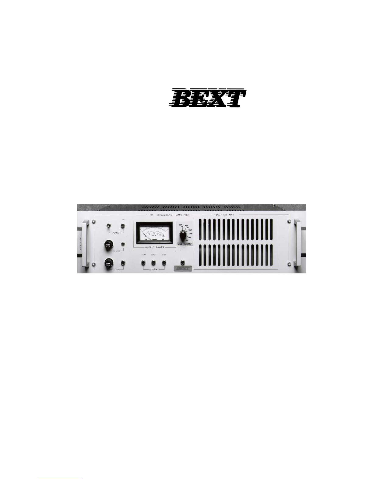
PJ 250
FM Power Amplifier
87.5 - 108 MHz Range
TECHNICAL
MANUAL
1
Page 2

INDEX
PRELIMINARY INSTRUCTIONS AND WARRANTY INFORMATION........................................... 2-3
INSTALLATION ....................................................................................................................................... 4
MECHANICAL / ELECTRICAL .............................................................................................................. 4
OPERATION ........................................................................................................................................... 4-5
TECHNICAL SPECIFICATIONS ............................................................................................................. 6
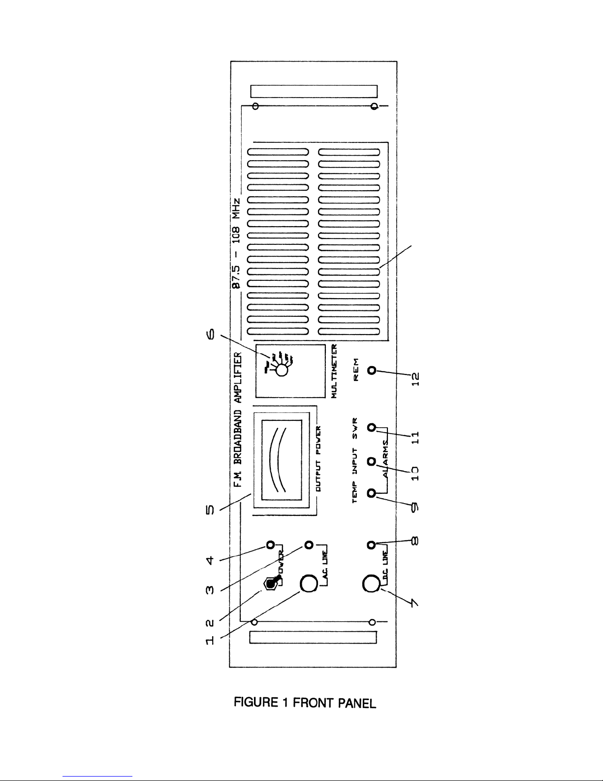
FRONT AND REAR PANEL CONTROLS .............................................................................................. 7
FIGURE 1 FRONT PANEL ....................................................................................................................... 8
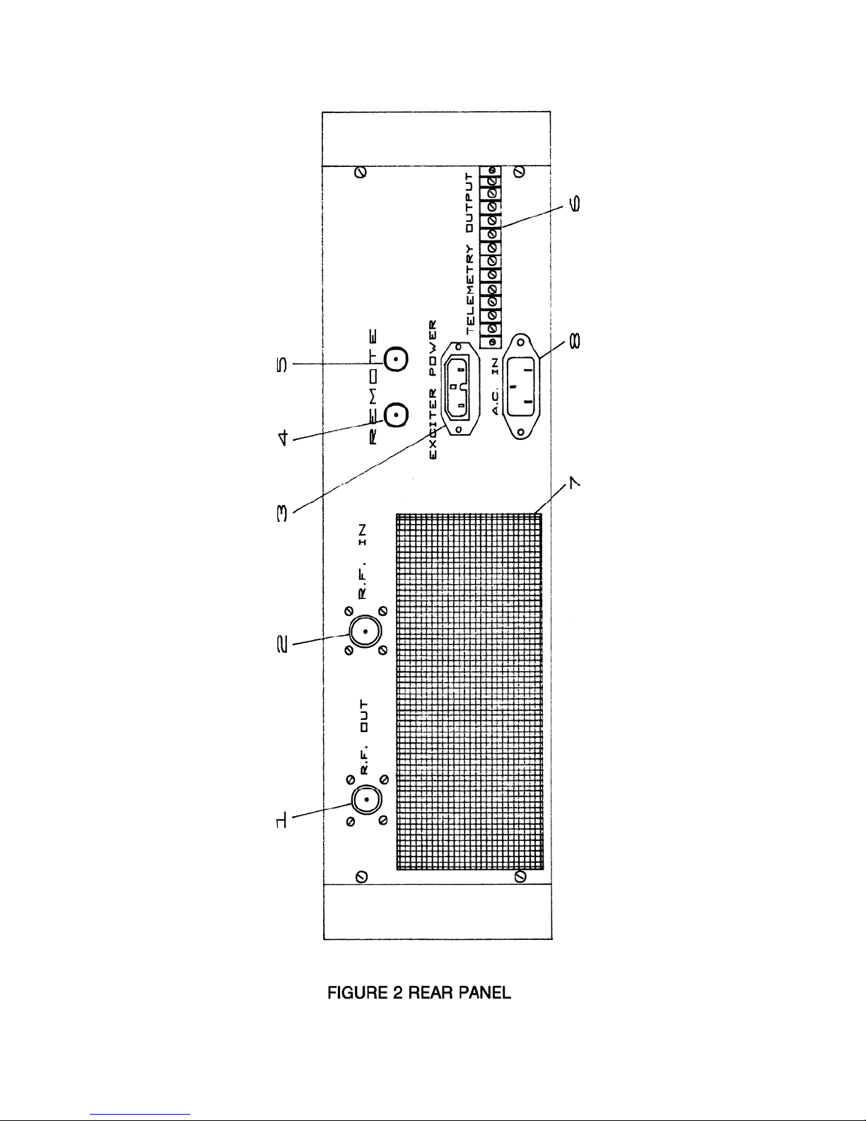
FIGURE 2 REAR PANEL .......................................................................................................................... 9
GENERAL AND ELECTRICAL DESCRIPTION ............................................................................. 10-11
RECOMMENDED TEST EQUIPMENT ................................................................................................. 11
MAINTENANCE AND ADJUSTMENTS ......................................................................................... 11-14
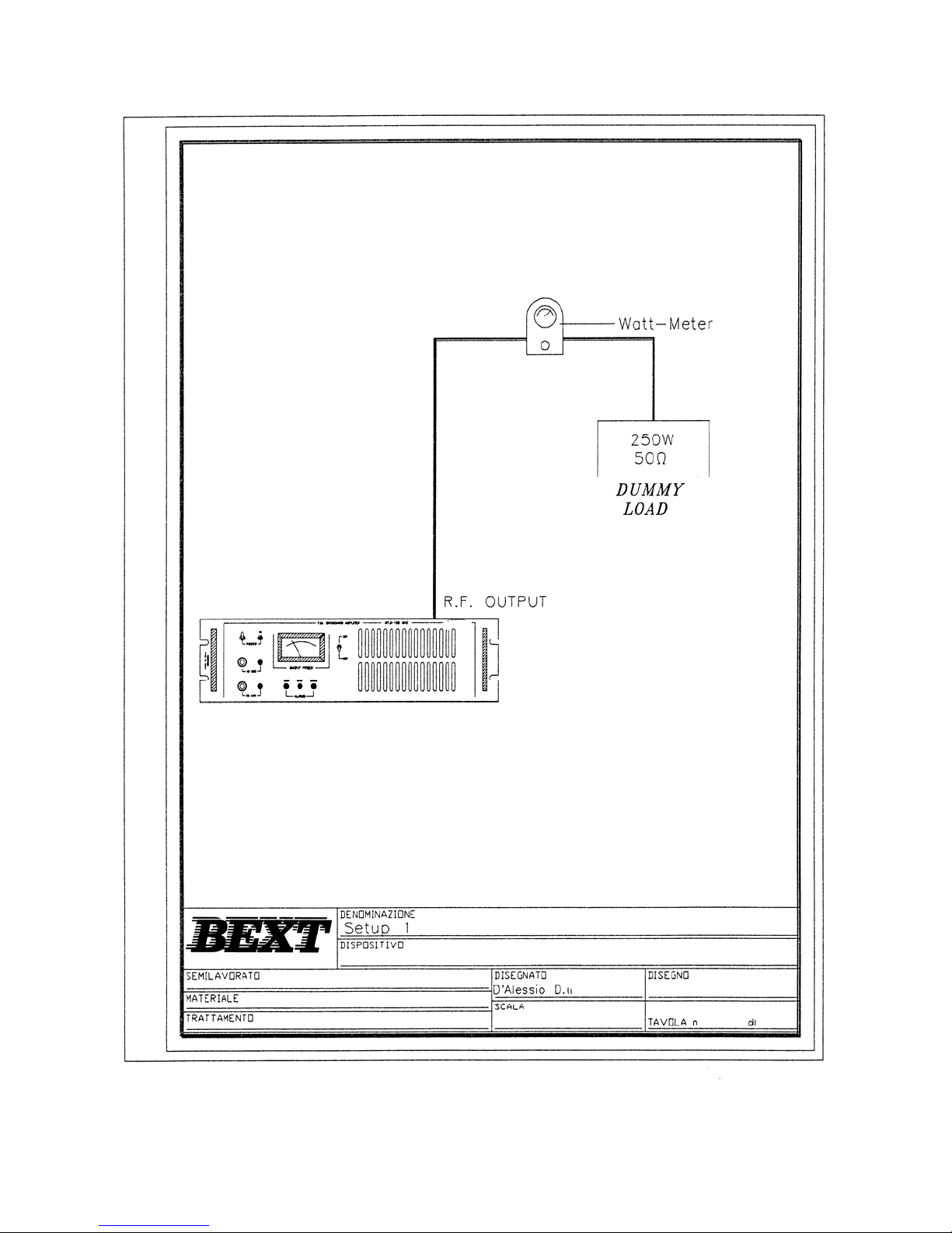
SETUP 1 ................................................................................................................................................... 15
SETUP 2 ................................................................................................................................................... 16
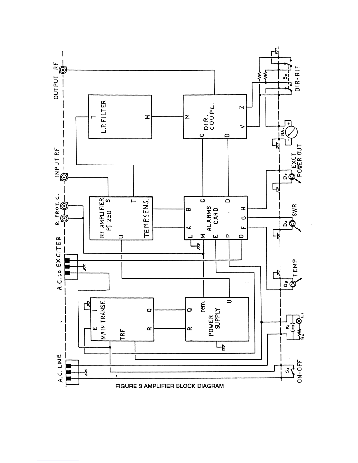
FIGURE 3 AMPLIFIER BLOCK DIAGRAM ......................................................................................... 17
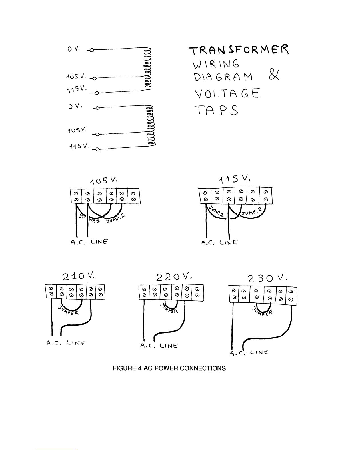
FIGURE 4 AC POWER CONNECTIONS ............................................................................................... 18
FIGURE 5 SCHEMATIC, UNREGULATED POWER ........................................................................... 19
FIGURE 6 SCHEMATIC, REGULATED POWER ................................................................................ 20
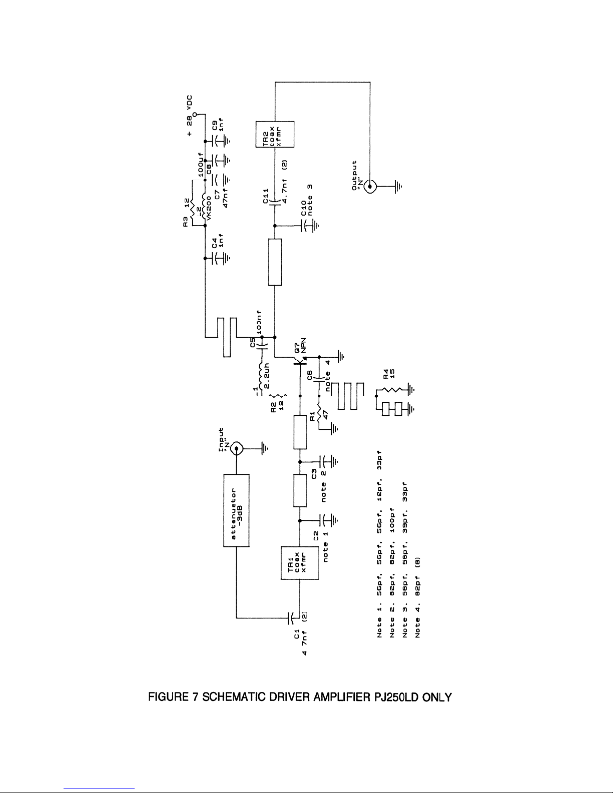
FIGURE 7 SCHEMATIC DRIVER AMPLIFIER (PJ250 L/D ONLY) .................................................. 22
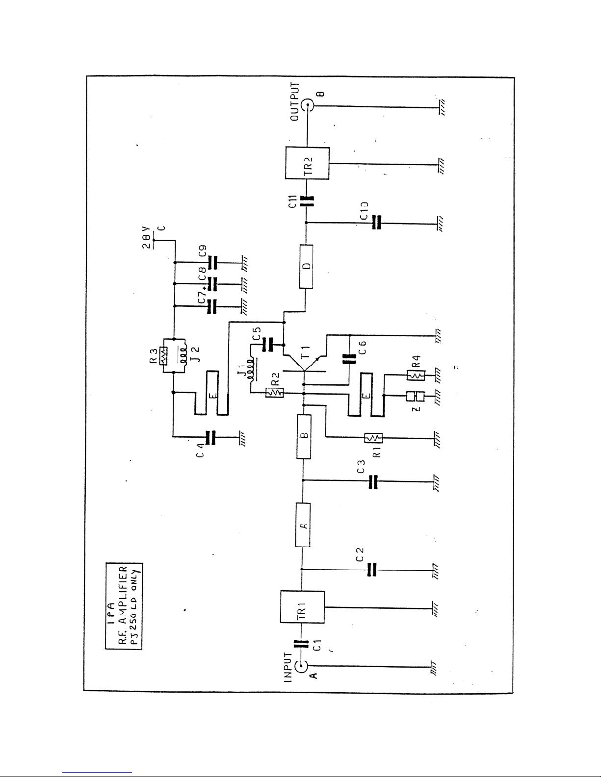
FIGURE 7a IPA RF AMPLIFIER (PJ250 L/D ONLY) ........................................................................... 23
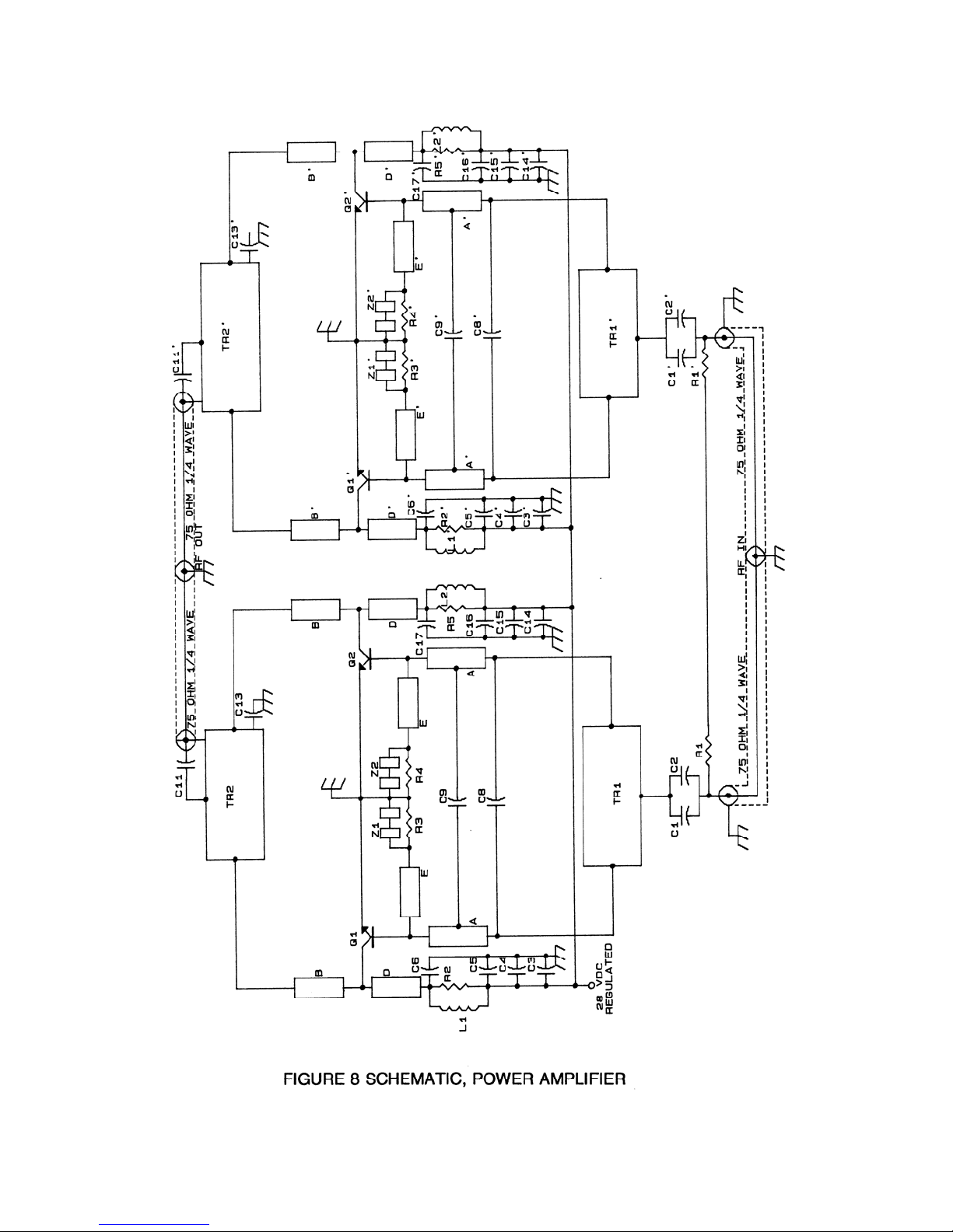
FIGURE 8 SCHEMATIC, POWER AMPLIFIER ................................................................................... 25
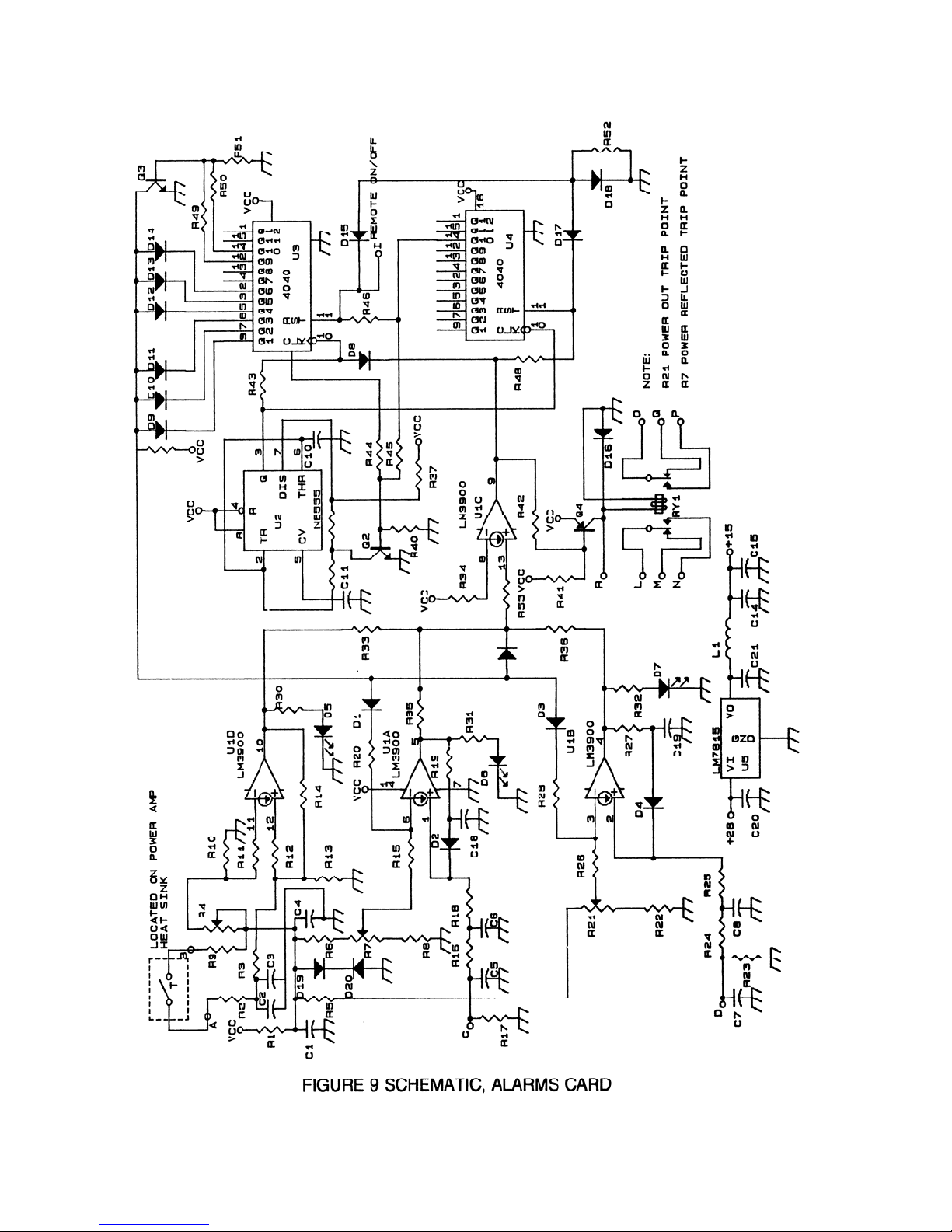
FIGURE 9 SCHEMATIC, ALARMS CARD .......................................................................................... 27
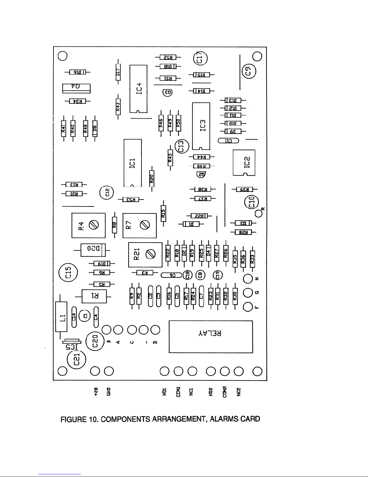
FIGURE 10. COMPONENTS ARRANGEMENT, ALARMS CARD .................................................... 28
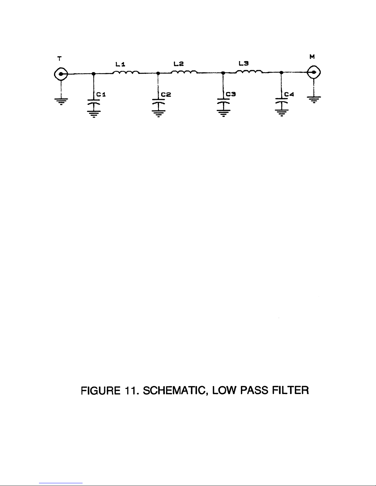
FIGURE 11. SCHEMATIC, LOW PASS FILTER .................................................................................. 31
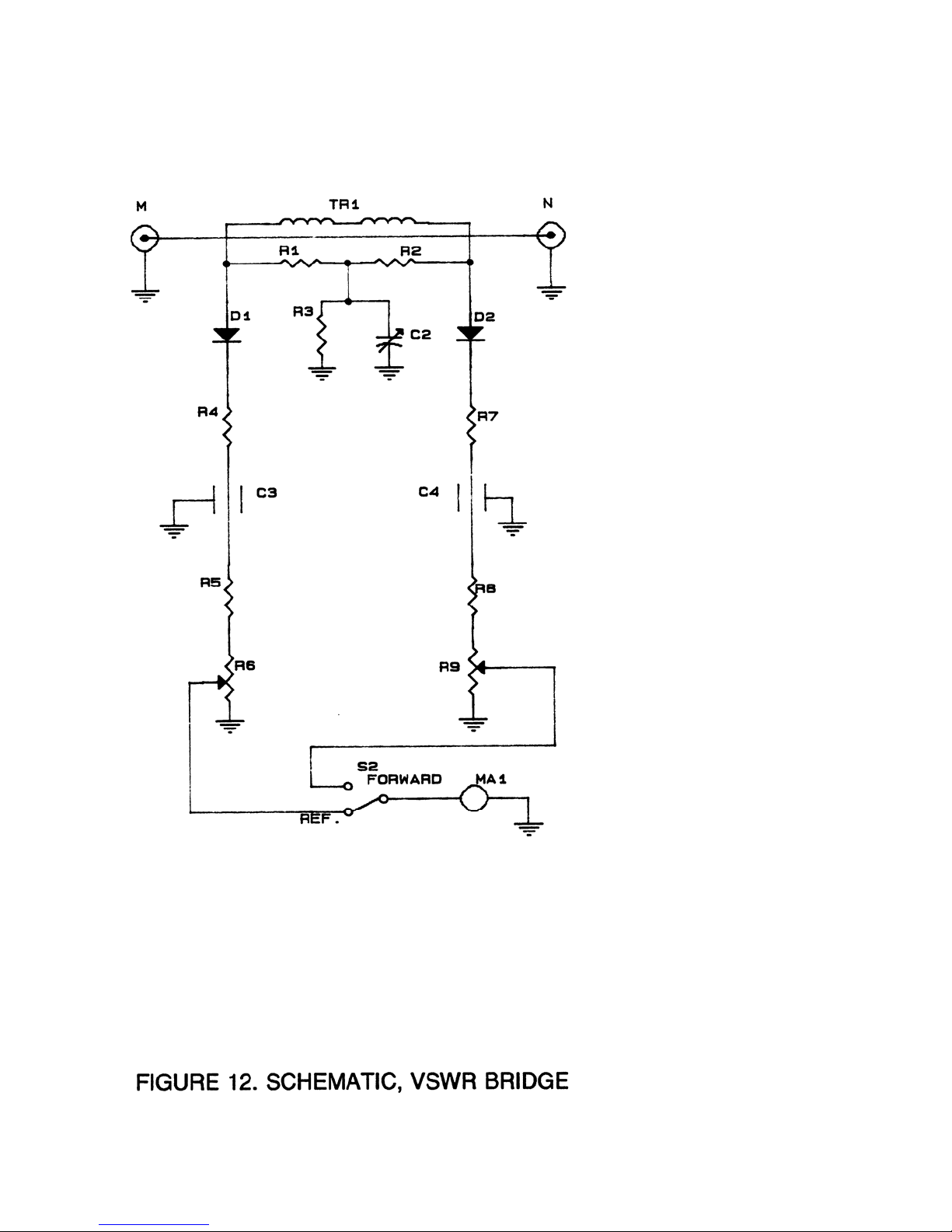
FIGURE 12. SCHEMATIC, VSWR BRIDGE ......................................................................................... 33
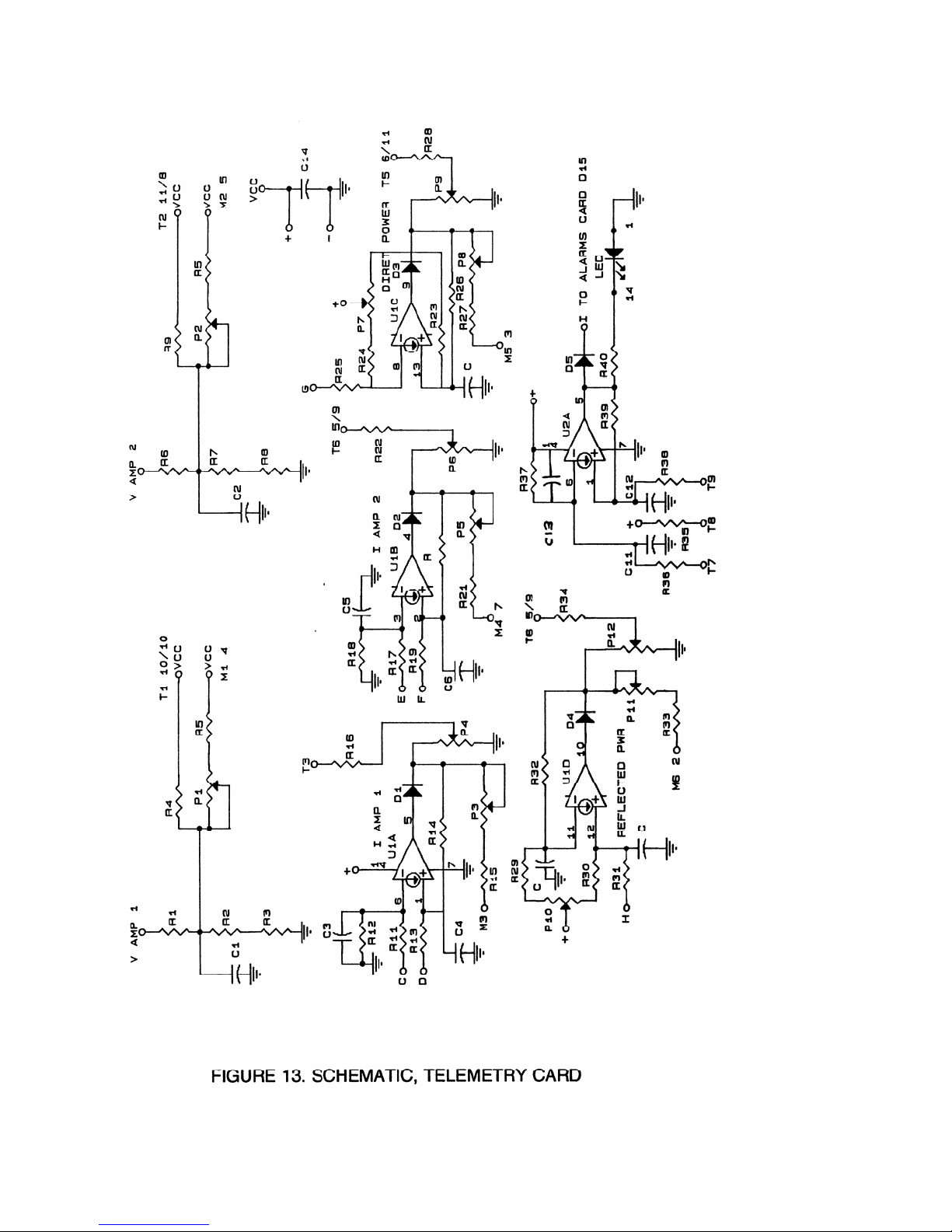
FIGURE 13. SCHEMATIC, TELEMETRY CARD ................................................................................ 34
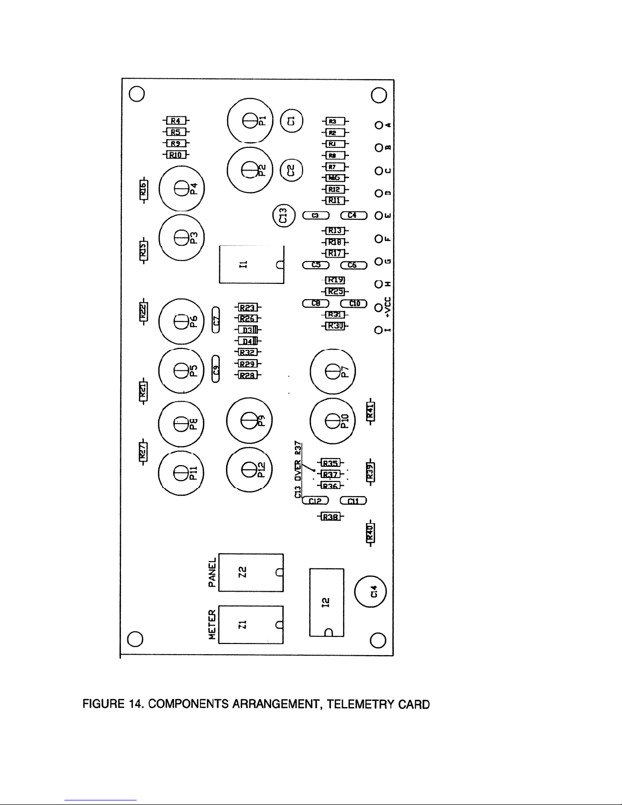
FIGURE 14. COMPONENTS ARRANGEMENT, TELEMETRY CARD ............................................. 35
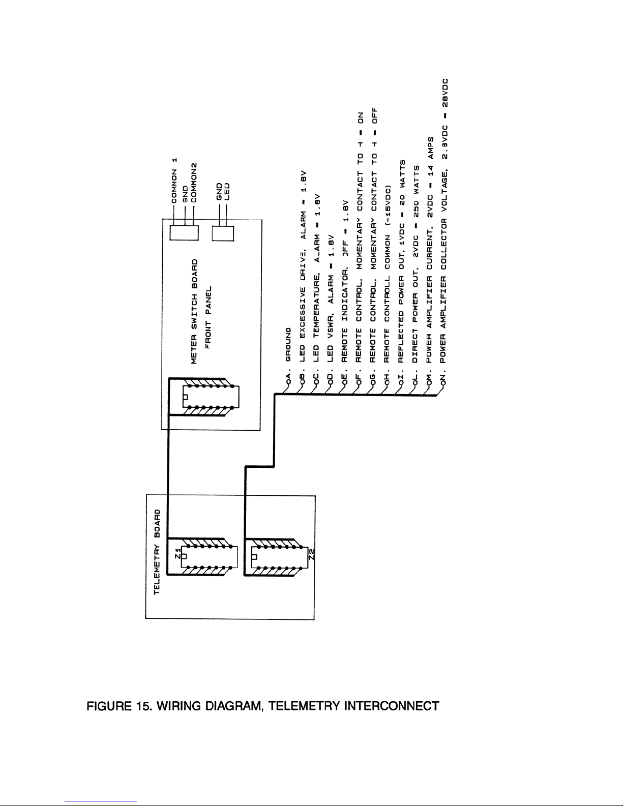
FIGURE 15. WIRING DIAGRAM, TELEMETRY INTERCONNECT ................................................. 36
PARTS LIST POWER SUPPLY .............................................................................................................. 21
PARTS LIST RF DRIVER BOARD (PJ250 L/D ONLY) ....................................................................... 24
PARTS LIST RF POWER AMPLIFIER .................................................................................................. 26
PARTS LIST LOW PASS FILTER .......................................................................................................... 32
PARTS LIST DIRECTIONAL COUPLER .............................................................................................. 32
PARTS LIST ALARMS PROTECTION CARD ................................................................................ 29-30
PARTS LIST TELEMETRY CARD ........................................................................................................ 37
2
Page 3

PRELIMINARY INSTRUCTIONS AND
WARRANTY INFORMATION
1. Please observe all safety precautions when handling this unit. This equipment contains
dangerous currents and voltages.
2. This manual is written as a general guide for those having previous knowledge and
experience with this kind of equipment. It is not intended to contain a complete statement
of all safety precautions which should be observed by personnel in using this or other
electronic equipment.
3. BEXT Inc. does not assume responsibility for injury or damage resulting from improper
procedures or practices of untrained/unqualified personnel in the handling of this unit.
4. Please observe all local codes and fire protection standards in the operation of this unit.
5. CAUTION: Always disconnect power before opening covers or removing any part of this
unit. Use appropriate grounding procedures to short out capacitors and high voltage
points before servicing.
6. Any damage to the goods must be reported to the carrier in writing on the shipment
receipt. Any discrepancy/damage discovered subsequent to delivery shall be reported to
BEXT Inc. within five days of receipt.
7. BEXT Inc. extends to the original end-user purchaser all original manufacturer’s
warranties which are transferable and all claims are to be made directly to BEXT Inc. per
indicated procedures.
8. All manufacturer’s warranties will be supported by BEXT Inc. to ensure precise and
speedy service where possible.
9. BEXT Inc. shall not be liable for damages of any nature arising out of or in connection
with the product or its use thereof.
10. BEXT’s warranty shall not include:
10.1 Reshipment of the unit to BEXT for repair purposes.
10.2 Any unauthorized repairs/modifications.
10.3 Incidental/consequential damages as a result of any defect.
10.4 Nominal non-incidental defects.
10.5 Reshipment costs or insurance of the unit or replacement units/parts.
11. Warranty shall commence on the invoice date and for the period of the manufacturer’s
warranty.
3
Page 4

12. To claim your rights under this warranty:
12.1 Contact the dealer or distributor from whom this product was purchased. Describe
the problem and ask if they have an easy solution. Dealers and distributors are
supplied with information on problems which may occur and usually can repair
the unit more quickly than going directly to the factory. It is also often true that
errors in installation or use will be discovered by your dealer.
12.2 If your dealer cannot help, contact BEXT Inc. at (619) 239-8462 and explain the
problem. If it is determined that the unit needs to be returned to the factory,
BEXT will provide a return authorization number with instructions.
12.3 When you receive the return authorization, you can return the unit. Pack the unit
carefully for shipment. Preferably, use the original packing materials and assume
that the shipping carton will be dropped several times during the transportation
process. We recommend the use of UPS or similar freight services and would
discourage the use of the postal system. The customer assumes the risk of loss,
(i.e. BEXT Inc., is not responsible for damage or loss) until the package is
received by BEXT, so we advise taking out insurance for the full replacement
value of the unit. Ship the unit PREPAID to the address specified by BEXT’s
service manager on the return authorization. DO NOT RETURN UNITS
WITHOUT A RETURN AUTHORIZATION, AS THEY WILL NOT BE
ACCEPTED.
12.4 Be sure to enclose a written descriptive statement of the problem experienced and
a copy of your original invoice establishing the starting date of the warranty.
13. BEXT Inc. reserves the right to modify the design and specifications of the equipment in
this manual without notice.
14. Replacement and warranty parts may be ordered from the address below. Be sure to
include equipment model and serial number and part description and part number.
BEXT Inc.
1045 Tenth Avenue
San Diego, CA 92101 USA
(619) 239-8462 • FAX (619) 239-8474
24-Hour Pager: (619) 529-4711
e-mail: [email protected]
http://www.bext.com
4
Page 5

INSTALLATION
INSTALLATION
A. Read the BEXT warning, shipping and warranty information at the front of the manual.
B. Handle the unit as carefully as possible.
C. Unpack the amplifier and, before any other operation, check that the amplifier isn't damaged and
that all controls on the front and rear panel are in good condition.
D. Save the original packing materials.
MECHANICAL / ELECTRICAL
A. Operate the unit with adequate ventilation in a relatively cool environment.
B. Check that the A.C. supply is adequate for the expected power consumption and that the line
voltage matches the taps in the unit with minimal line voltage variation. If the line voltage
fluctuates frequently and extensively, a voltage regulator is recommended. A surge/transient
C. Never operate the unit without a dummy load or properly matched antenna load.
suppression system is also highly recommended.
D. If you are going to operate solid state equipment as a final amplifier in a very crowded
transmitting site, it is suggested that a fundamental frequency/cavity bandpass filter be inserted in
the line between the equipment and the antenna. The BEXT staff can assist you.
OPERATION
A. Open the cover and check the voltage setting on the transformer. The transformer offers several
taps for different voltages. If it is found necessary to move the taps, move only the A.C. primary
taps. Do not move the fan wires which are connected to the same terminal block.
B. Turn the "power adjust" of the exciter to zero and turn the power switches to the "off" position of
both the amplifier and the exciter. Set the exciter to the desired frequency of operation.
C. Connect the RF output of the exciter to the input of the amplifier. The input of the amplifier uses
a type "N" connector. Use good quality cable to prevent RF leakage. Connect the RF output of
the amplifier to a suitable dummy load or antenna.
D. Connect the exciter A.C. cord to the plug provided on the rear of the amplifier. This will provide
protection by shutting down the exciter when an alarm condition is detected by the amplifier.
Connect the amplifier A.C. cord to the A.C. supply.
E. Turn the amplifier power on. The power indicator should come on and the fans should begin
running. CAUTION:
not come on the user should check the following:
Do not apply RF drive unless the fans are running properly. If the unit does
1. Check the A.C. line fuses.
2. Check the A.C. line connections.
3. Check the internal transformer taps and the fan/blower itself.
F. Turn on the exciter. The power indicator light should come on and a lock indication should come
on. The exciter blower should also be running. Check all power supply voltages on the amplifier
and exciter to ensure they are correct before proceeding. The amplifier voltage should be
approximately 28 volts. Exciter voltages will be marked on the front panel of the exciter and will
vary with the type of exciter.
G. Set the power meter switch to the forward power position on both the exciter and the amplifier.
Slowly advance the power on the exciter until RF power output is observed on both meters.
Check now for VSWR. If the standing wave reading appears normal (less than 1.5:1) then
proceed to raise the power. The voltage on the amplifier should remain steady at approximately
5
Page 6

28 volts. The exciter PA voltage will change with drive level. Efficiency of the amplifier will be
approximately 60%.
H. Maximum VSWR should never exceed 2:1. Should the amplifier see a VSWR higher than this it
will trip the alarm board and shut down both the amplifier and the exciter.
I. Alarm conditions which will shut down the amplifier are: VSWR of greater than 2:1; excessive
power output(higher than the rating); high temperature. Should the amplifier sense any of the
above conditions it will shut down and automatically attempt to restart after 90 seconds and will
attempt 4 times to restart. The unit will then shut down for 15 minutes; and again go through the
4 restart attempts. After four of these cycles the unit will go into a permanent shutdown. The
power must be recycled to reset the alarm circuits. The operator should always look at the front
panel to determine which alarm shut the unit down. This will aid in locating conditions which are
causing the problem should one exist.
J. Telemetry is provided on the rear panel to monitor the voltage, current, power, and reflected
power of the amplifier. Terminals are also provided to enable putting the amplifier in standby via
a momentary contact closure. A momentary contact closure will also reactivate the amplifier. A
second input is provided which will place the amplifier and exciter in standby. Two "BNC"
connectors labeled "REMOTE" are provided on the rear of the amplifier and another on the rear
of the exciter. Connect the exciter remote BNC to the either of the amplifier remote BNC
connectors. By placing a ground on the center pin of the second BNC connector the RF drive will
be shut down to the amplifier. This can be accomplished by placing a ground on the exciter
remote connection only.
K. High VSWR conditions may be caused by icing of the antenna during winter storms. Leaking
transmission lines may have moisture or damage may occur to the antenna itself. Do not attempt
to reset the alarm levels to circumvent an external problem. This will cause damage to the
expensive RF output transistors and void the warranty. The user should also provide effective
lightening protection such as sorted quarter wave stubs on the transmission line. Power line
protection is also recommended as lightening hits many time come in on the power or telephone
lines. The telemetry lines should also be protected if connected to the telephone lines or lines
exiting the building. A good grounding system will help ensure many years of reliable operation
from your solid state equipment.
6
Page 7

TABLE A
TECHNICAL SPECIFICATIONS
A.C. Supply 100-130 V or 198-250 V
50-60 Hz
Cooling Forced Ventilation
Frequency Range from 87.5 to 108 MHz or
from 66 to 75 MHz
Power Output Max 300 W, typ. 250 W (Note: Limit power to
250W to maintain a good level of reliability.
RF Drive Power approximately 25 W for
P out=250 W
RF Input Impedance 50 ohm
RF Output Impedance 50 ohm
I/O Connector Standard "N" Connector
Harmonic and Spurious Signal Suppression meets or exceeds FCC and CCIR regulations
Power Consumption 800 w
TABLE B
DIMENSIONAL AND ENVIRONMENTAL SPECIFICATIONS
Cabinet Dimension 122mm(4.8")H x 420mm(16.54")W
350mm(13.78")D
Panel Size 483mm(19")W x 132mm(5.2")H
Operating Temperature -10°C to 45°C
Humidity 90% Max, Non Condensing
Weight 19 Kg
The protection acts for excessive SWR, over-temperature and overdrive. It indicates the problem with
warning lights and disables the pilot exciter.
7
Page 8

FRONT AND REAR PANEL CONTROLS
A. FRONT PANEL
1. Fuse 6.3 amps 220 Vac or 15 amps 120Vac
2. On/Off A.C. power switch
3. A.C. Blown Fuse Indicator
4. A.C. Power Indicator
5. Multimeter
6. Multimeter Switch
7. D.C. Fuse 20 amps
8. D.C. Blown Fuse Indicator
9. Temperature Alarm Indicator Lamp
10. Excessive Drive Alarm
11. VSWR Alarm Indicator
12. Remote Disable Indicator
B. REAR PANEL
1. RF output connector Type "N"
2. RF input connector Type "N"
3. Accessory AC plug for exciter (max 3 amps)
4. Remote protection connector Type "BNC", ground to activate
5. Remote protection connector Type "BNC". ground to activate
6. Telemetry Connections
7. Air Duct
8. A.C. Line Input
8
Page 9
9
Page 10
10
Page 11

PJ250 GENERAL DESCRIPTION
EXTERNAL DESCRIPTION
The PJ250 is housed in a 3U 19" rack, on the front panel the alarm indicators are placed in a central
position, the mains switch and the meter for the forward and reflected power. On the rear panel the RF
INPUT and RF OUTPUT connectors are located, together with the interlock connectors, one of BNC type
and one VDE female, the main voltage input.
ELECTRICAL DESCRIPTION
The PJ250 is a power amplifier working on the 87.5-108 MHz band with an output power in excess of
250W and a drive level of about 25W. This amplifier uses a RF module composed of four amplification
stages (MRF 317), with power supplies fixed with the RF module on cooling ribs to obtain a high
dissipation. A built in low pass filter suppresses the harmonic contents below the FCC and CCIR
requirements. A protection system protects the amplifier against thermal problems, excessive input drive
power and excessive SWR inside the amplifier or along the feeder. This system provides an automatic
reset to initial conditions when the problem ceases.
METERS AND INDICATORS
The forward and reflected power of the amplifier are read by the analog multimeter (11.Fig.1) and
selected by the selector (12.Fig.l) on the front panel. Various led indicators indicate the alarm conditions
caused by thermal problems (3.Fig.l), excessive input drive power (4.Fig.l) and excessive SWR (5.Fig.l).
A green indicator confirms the amplifier is operational (10.Fig.1).
PROTECTION CIRCUITS
The protection circuits put the amplifier in stand-by in the case of a fault condition. After 90 seconds the
protection reactivates the amplifier if the fault has disappeared. If not, this process is repeated 4 times, at
the end of which the amplifier stays disabled for 15 min; after 15 min, if the trouble persists, the
protection performs another four cycles and then disables the amplifier indefinitely. If during these cycles
the anomaly disappears and the amplifier works regularly for more than 15 min, the counting system is
reset and the original conditions established.
NOTE: the intervals described are nominal.
ELECTRICAL DESCRIPTION
INTRODUCTION
This section describes the overall working theory of the PJ250. For ease of description the amplifier is
subdivided into subassemblies that will be discussed in detail below. The block diagram is illustrated in
Fig.5.
POWER SUPPLY
The power supply comprises of a P.C. board fitted to the cooling fins and is accessible from the lower
part of the amplifier, unscrewing the fixing bolts of the cooling fins as shown in Fig.4. A mains
transformer has a selectable input for voltages between 110 and 240 V and two outputs:
"A": 31 V, "B": 18 V.
The output "A" drives the RF modules. Output "B" supplies the ALARMS CARD; inside this circuit a
rectifying and stabilization circuit provides the +15 V needed by the electronics.
ALARMS CARD
11
Page 12

This module is composed of a board shielded by a metal box mounted on the left side near the rear panel,
as shown in Fig.3. on this board, the electronics detect any system anomaly such as excessive SWR,
internal or antenna, over-temperature or overdrive, This module will also, whenever possible, reset the
system to its original conditions, after a fault has occurred.
RF POWER AMPLIFIER
The module is placed in the upper right side of the amplifier. This module is totally shielded and placed
on a heat sink (see Fig.3). This circuit delivers 300W with 25-30W of drive and is supplied by a dedicated
power supply. The quiescent parameters of each module are:
Vdc=28V Ia=15A Pout=250 W
The active devices employed are BJT NPN MOTOROLA (MRF317).
LOW PASS FILTER
This filter is fitted in a metallic box mounted on the heat sink on the right position as shown in Fig.3.
Thanks to this low pass filter the harmonic suppression is greater than 75 dBm.
DIRECTIONAL COUPLER
This circuit is placed on the upper right side of the amplifier and fitted on the rear panel as shown in
Fig.3. This module makes the measurement of the forward and reflected power.
RECOMMENDED TEST EQUIPMENT
INSTRUMENT TYPE SUGGESTED MODEL CRITICAL SPECIFICATIONS
Non Inductive Bird 50 ohm P > 250 W
Dummy Load
Spectrum Analyzer Advantest 10KHz-3.5GHz
MOD. R4131D
FM Monitoring R/S
Demodulator MOD. F.A.M.
Digital Multimeter MOD. Metrix
Calibrated in-line Bird MOD. 43 50 ohm
Wattmeter with Sample
Exciter BEXT Frequency 87.5-108MHz
MOD TEX 30 Pout from 2W to 30W
Dummy Load 25 ohm P 500W
MAINTENANCE
INTRODUCTION
The following section provides general maintenance information and electrical adjustment procedures for
the PJ250 Amplifier. Maintenance is divided into categories dependent upon the complexity of the
procedure and the test equipment required to complete the maintenance.
12
Page 13

WARNING! WARNING! WARNING!
When the amplifier is operated with the top cover removed, hazardous voltages are accessible on the A.C.
line voltage selector and heavy currents are accessible on the exposed terminals of the power supply filter
capacitor and power transistors mounted on the RF amplifier heat sink assembly. Use the insulated tuning
tool provided for any adjustment and do not touch any component within the amplifier when power is
applied. Ensure all primary power is disconnected from the amplifier before attempting equipment
maintenance.
FIRST LEVEL MAINTENANCE
ORDINARY MAINTENANCE
The only regular maintenance needed by the PJ250, is the periodic replacement of the blowers, and the
cleaning of dust filters and any dust accumulated inside the amplifier. The time between overhauling of
the blowers depends upon several environmental factors, temperature, humidity, dust pollution etc.,
Blowers should be checked every 6 months and replaced if noisy. They should be replaced any way after
18 months of service.
SECOND LEVEL MAINTENANCE
CARDS REPLACEMENT
This section contains useful information for card replacement.
WARNING! TO RE-INSTALL CARDS SIMPLY FOLLOW THE REVERSE PROCEDURE.
POWER SUPPLY REPLACEMENT
1) open the top and bottom covers.
2) Remove the four screws (three external and one internal) of the Power Supply section placed
under the RF section.
3) From the bottom of the amplifier, open the power supply section taking care not to break the
wires connected to the card.
4) Disconnect the four fasteners placed on the power supply, and unsolder the other wire.
5) Extract the power supply section.
ALARMS CARD REPLACEMENT
1) Open the top cover.
2) Remove the screws fixing the card on the left side of the amplifier.
3) Take note of the position of wires placed on the rear of the metal box.
4) Unsolder the wires placed on the rear of the metal box.
5) Extract the Alarms card.
DIRECTIONAL COUPLER REPLACEMENT
1) Open the top cover.
2) Remove the fixing screws of the "N" type output connector (1.Fig.2).
3) Unsolder the output cable (RG 303 type) of the low-pass filter placed on the RF section.
4) Take note of the position of the four wires going out of the directional coupler and unsolder them.
5) Extract the Directional Coupler.
TRANSFORMER REPLACEMENT
1) Open the top and bottom covers.
2) Remove the central fixing bolt of the transformer.
13
Page 14

3) Take note of the position of the transformer’s wires connected to the terminal block placed on the
metal support of the transformer (U.S. version), while for the standard version the wires of the
fuse and of the switch should be unsoldered.
4) Disconnect these wires from the terminal block (only for the U.S. version).
5) Unsolder the two wires connecting the transformer with the Alarms card.
6) Disconnect the fastener of the transformer placed on the diode bridge fixed on the central chassis
of the amplifier.
7) Extract the transformer.
FAN REPLACEMENT
1) Open the top and bottom covers.
2) Remove the four screws of the front panel.
3) Slide the front panel slowly.
4) Remove the fixing screws of the fan to the two rails.
5) Break the straps of the fan’s wires.
6) Disconnect the fasteners connected to the top of the fan (some units may not be fitted with
fasteners; in this case desolder the wires).
7) Extract the fan.
INTERNAL ADJUSTMENTS
POWER SUPPLY ADJUSTMENT
No adjustments are needed after this board has been changed.
DIRECTIONAL COUPLER BALANCING (PWR MEASURE)
1) Place the DIR/REF selector (12.Fig.1) to the REF position.
2) Connect (1.Fig.2) a non inductive dummy load 50 ohm / 250W to RF output with a through
wattmeter (e.g. BIRD mod.43) in series as shown in SETUP 1.
3) Set the exciter power to obtain 250W on the through external wattmeter.
4) Now, adjust variable capacitor C2 placed on the directional coupler to obtain the minimum value
on the meter, very near to zero.
FORWARD AND REFLECTED POWER ADJUSTMENT
1) Perform SETUP 1, and increase the amplifier’s output power to 250W (on the external
wattmeter).
2) Place the DIR/REF selector (12.Fig.1) to the DIR position.
3) Adjust trimmer R9 placed on the directional coupler so that the same reading is obtained on the
PJ250 meter.
4) Switch off the amplifier.
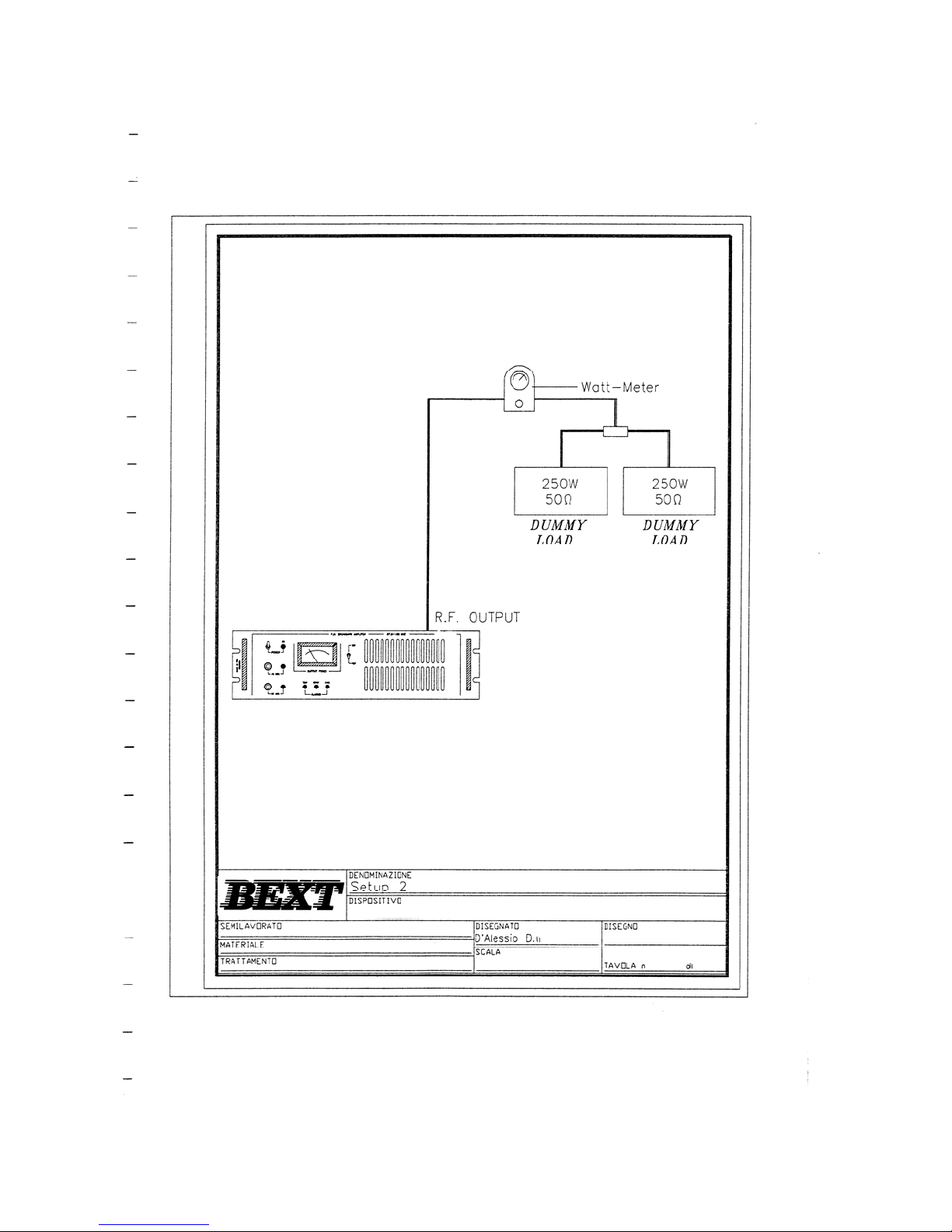
5) Connect a dummy load 25 ohm 500W (2 dummy loads 50 ohm 250W in parallel) with a through
wattmeter (e.g.. BIRD mod.43) in series, set for the reading of reflected power (SETUP 2).
6) Adjust the drive power to minimum and switch on the amplifier again.
7) Adjust the output power of the exciter to obtain a reading of 25W of reflected power on the
external wattmeter.
8) Adjust trimmer R6 placed on the directional coupler to obtain the same reading on the PJ250
meter.
ALARMS CARD ADJUSTMENT
There are three trimmers on the Alarms card that are necessary to adjust the alarm thresholds: overtemperature - (R4); VSWR - (R7); and overdrive - (R21).
14
Page 15

CALIBRATION OF OVER-TEMPERATURE ALARM THRESHOLD
1) Short-circuit the thermal switch placed on the RF section’s heat sink.
2) Adjust the trimmer, R4, placed on the Alarms card until the over-temperature protection is
activated, and the TEMP led lights up (3.Fig.1).
3) Remove the short-circuit on the thermal switch and verify that the TEMP led goes out.
4) Repeat this procedure again to verify the correct trimmer R4 adjustment.
CALIBRATION OF VSWR
1) Connect a dummy load, 25 ohm 500W (two dummy loads 50 ohm 250W in parallel) with a by-
pass wattmeter in series (e.g., BIRD mod.43) set for reflected power reading (SETUP 2).
2) Adjust the output power of the exciter to obtain a reading of 25W of reflected power on the
external wattmeter and the PJ250 meter.
3) Adjust the trimmer, R7, placed on the Alarms card until the R.O.S. protection is activated, and the
SWR led lights up (5.Fig.l).
4) Decrease the output power of the exciter and wait for the SWR led to go out (automatic
protection cycle).
5) Increase the output power of the exciter again over the R.0.S. threshold of 25W, and verify once
again, that the SWR led lights up (5.Fig.1).
CALIBRATION OF OVER-DRIVE ALARM THRESHOLD
1) Adjust the driver power to minimum and switch on the amplifier.
2) Place the DIR/REF selector (12.Fig,l) to the REF position.
3) Connect (1.Fig.2) a non inductive dummy load 50 ohm 250W to the RF output with a through
wattmeter (e.g., BIRD mod.43) in series as shown in the SETUP 1.
4) Set the exciter power to obtain 250W on the through external wattmeter and on the PJ250 meter.
5) Increase the output power of the exciter again until a reading of 270W on the PJ250 meter is
obtained.
6) Adjust the trimmer, R21, placed on the Alarms card until the over-drive protection is activated,
and the INPUT led lights up (4.Fig.1) with immediate shutdown of the amplifier.
7) Decrease the drive power of the exciter and wait for the INPUT led to go out.
8) Increase the drive power of the exciter again over the overdrive threshold of 270W, and verify,
that the INPUT led lights up (4.Fig.1).
RF SECTION ADJUSTMENT
No adjustment is required inside the RF section because it's a factory adjusted module; if calibration is
necessary, please send the module to your local distributor.
LOW-PASS FILTER ADJUSTMENT
No adjustment is required inside the Low-Pass Filter module because it's a factory adjusted module; if
calibration is necessary, please send the module to your local distributor.
15
Page 16
SETUP 1
16
Page 17
SETUP 2
17
Page 18
18
Page 19
19
Page 20
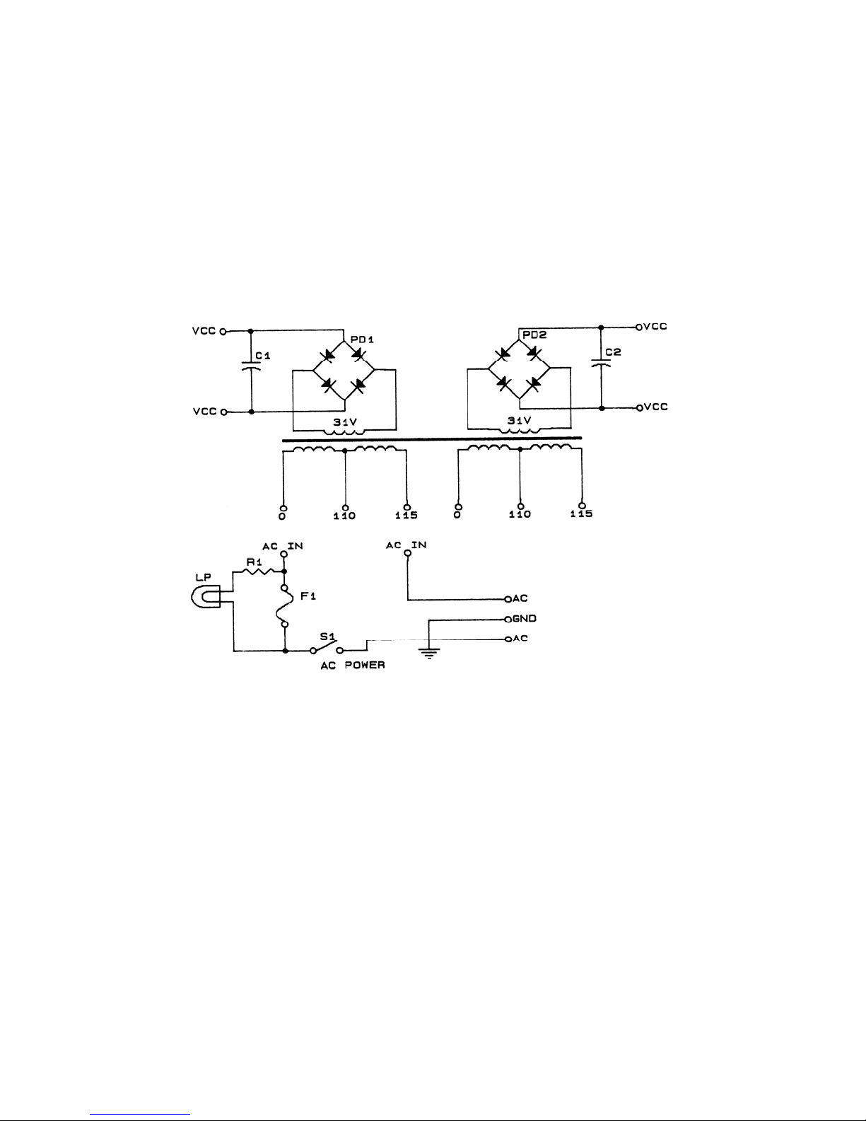
FIGURE 5 SCHEMATIC, UNREGULATED POWER
20
Page 21
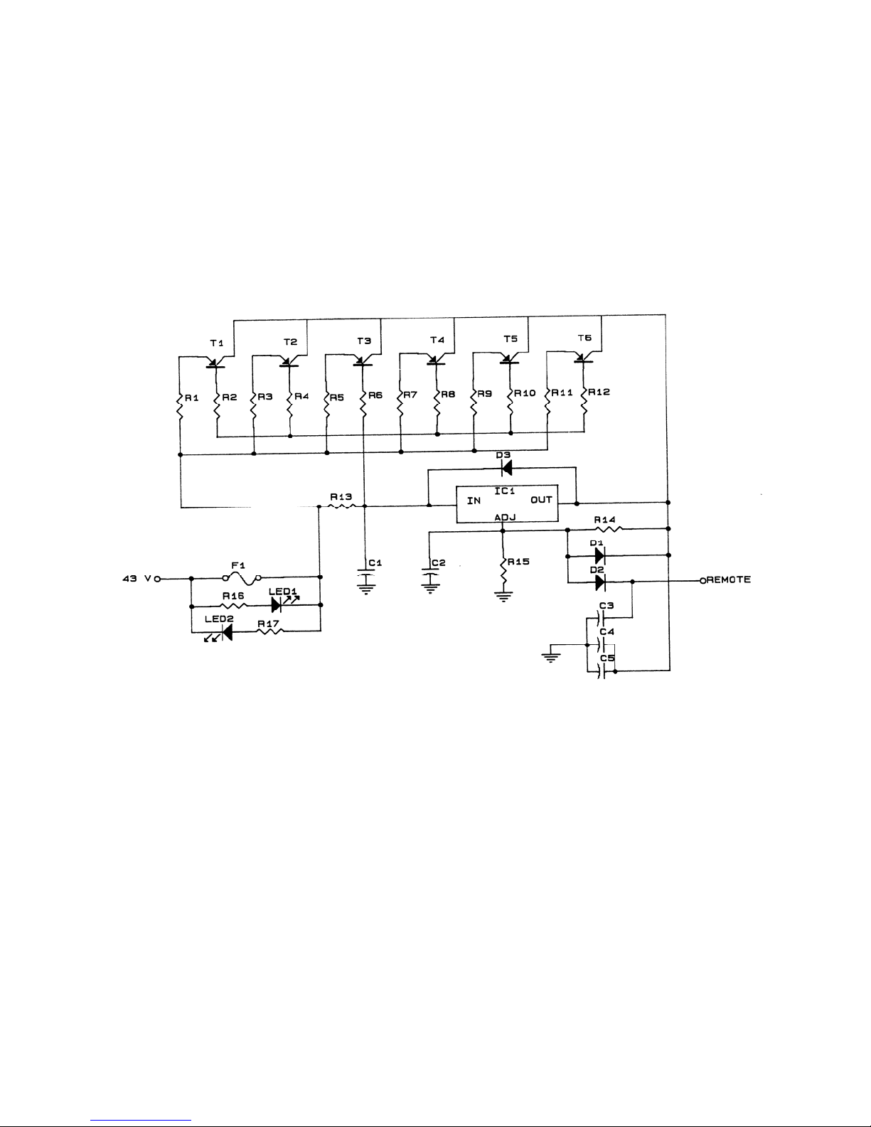
FIGURE 6 SCHEMATIC, REGULATED POWER
21
Page 22

PARTS LIST
POWER SUPPLY
UNREGULATED F2 Fuse 20 amp
C1 Capacitor Elec. 10 nF 63Vdc I1 IC, Regulator LM317HVK
C2 Capacitor Elec. 10 nF 63Vdc
LED1 Indicator LED, Red
F1 Fuse 6 amps (220 Vac) 15 amps LED2 Indicator LED, Green
(120 Vac)
R 1 Resistor WW 0.22 ohm 5 watt
PD Bridge Rectifier 100piv 25 amps R2 Resistor 5.6 ohm 1/2 watt
R3 Resistor WW 0.22 ohm 5 watt
S1 AC Power Switch 15 amp R4 Resistor 5.6 ohm 1/2 watt
R5 Resistor WW 0.22 ohm 5 watt
TRF Transformer, Power 31 Vac 20 R6 Resistor 5.6 ohm 1/2 watt
amp, 18Vac 1 amp, tapped R7 Resistor WW 0.22 ohm 5 watt
primary R8 Resistor 5.6 ohm 1/2 watt
R9 Resistor WW 0.22 ohm 5 watt
REGULATED R10 Resistor 5.6 ohm 1/2 watt
R11 Resistor WW 0.22 ohm 5 watt
C1 Capacitor Elec. 10µF 63Vdc R12 Resistor 5.6 ohm 1/2 watt
C2 Capacitor Elec. 10µF 35Vdc R13 Resistor WW 4.7 ohm 5 watt
C3 Capacitor Ceramic 4.7nF R14 Resistor 220 ohm 1/2 watt
C4 Capacitor Elec 100µF 63Vdc R15 Resistor 4.7K ohm 1/2 watt
C5 Capacitor Ceramic 47nF R16 Resistor 2.2K ohm 1/2 watt
R17 Resistor 2.2K ohm 1/2 watt
D1 Diode 1 N4003
D2 Diode 1 N4003
22
Page 23
23
Page 24
F
I
G
U
R
E
7a
24
Page 25

PARTS LIST
RF DRIVER BOARD (PJ250 L/D ONLY)
C1 Capacitor, Ceramic, Group of 2 - 4.7nF, 4.7nF
C2 Capacitor, Ceramic, Group of 5 - 56pF, 56pF, 56pF, 12pF, 33pF
C3 Capacitor, Ceramic, Group of 3 - 82pF, 82pF, 100pF
C4 Capacitor, Mica, Unelco 1nF
C5 Capacitor, Ceramic, 100nF
C6 Capacitor, Ceramic, group of 8 - 82pF each
C7 Capacitor, Ceramic, 47nF
C8 Capacitor, Elec 100µF 35Vdc
C9 Capacitor, Ceramic 1nF
C10 Capacitor, Ceramic, Group of 4 - 56pF, 56pF 39pF, 33pF
C11 Capacitor, Ceramic, Group of 2 - 4.7nF, 4.7nF
J1 Inductor 2.2µH
J2 Inductor VK200
T1 Transistor, RF Power, PT9783
TR1 Transformer RF Broadband 4:1
TR2 Transformer RF Broadband 4:1
Z Ferrite Bead
25
Page 26
26
Page 27

PARTS LIST
RF POWER AMPLIFIER
NOTE: The PJ200 Power Amplifier is one section or half of the PJ250 Amplifier, therefore the parts list
and schematic are common. The second half of the PJ250 Amplifier is a mirror image of the first half.
C1 Capacitor, Ceramic 4.7nF R1 Resistor 47 ohm 1 watt
C2 Capacitor, Ceramic 4.7nF R2 Resistor 12 ohm 1/2 watt
C3 Capacitor, Ceramic 47nF R3 Resistor 12K ohm 1/2 watt
C4 Capacitor, Elec 100µF 35Vdc R4 Resistor 12 ohm 1/2 watt
C5 Not Used R5 Resistor 12 ohm 1/2 watt
C6 Capacitor, Mica 1nF SEMCO
C7 Capacitor, Ceramic chip 470pF T1 RF Power Transistor MRF317
C8 Capacitor, Ceramic chip 12pF T1' RF Power Transistor MRF317
C9 Capacitor, Ceramic chip 47pF T2 RF Power Transistor MRF317
C10 Capacitor, Ceramic, Group of 2 T2' RF Power Transistor MRF317
33pF each
C11 Capacitor, Mica 1nF SEMCO TR1 RF Transformer Broadband 4:1
C12 Not used TR2 RF Transformer Broadband 4:1
C13 Capacitor, Mica 1nF SEMCO
C14 Capacitor, Ceramic 47nF Z1 Ferrite Bead
C15 Capacitor, Elec 100µF 35Vdc Z2 Ferrite Bead
C16 Not used
C17 Capacitor, Mica 1nF SEMCO
L1 Inductor VK200
L2 Inductor VK200
27
Page 28
28
Page 29
29
Page 30

PARTS LIST
ALARMS PROTECTION CARD
C1 Capacitor, Elec 10µF 16Vdc IC1 Quad OP Amp LM3900
C2 Capacitor, Ceramic 47nF IC2 Integrated Circuit NE555
C3 Capacitor, Ceramic 47nF IC3 IC Counter MC4040
C4 Capacitor, Ceramic 4.7nF IC4 IC Counter MC4040
C5 Capacitor, Ceramic 47nF IC5 IC Regulator LM7815
C6 Capacitor, Ceramic 4.7nF
C7 Capacitor, Ceramic 4.7nF L1 Inductor 220µH
CB Capacitor, Elec 33µF 35Vdc
C9 Capacitor, Elec 4.7µF 25Vdc Q1 Transistor BC237
C10 Capacitor, Elec 2.2µF 25Vdc Q2 Transistor BC237
C11 Capacitor, Ceramic 47nF Q3 Transistor BC140
C12 Capacitor, Elec 4.7µF 25Vdc Q4 Transistor BC140
C13 Capacitor, Elec 4.7µF 25Vdc
C14 Capacitor, Ceramic 47nF R1 Resistor 680 ohm 1/2 watt
C15 Capacitor, Elec 100µF 25Vdc R2 Resistor 100 ohm 1/4 watt
C16 Capacitor, Elec 4.7µF 25Vdc R3 Resistor 2.2K ohm 1/4 watt
C17 Capacitor, Elec 10µF 25Vdc R4 Resistor 22K ohm Pot
C18 Capacitor, Elec .47µF 25Vdc R5 Resistor 1 K ohm 1/4 watt
C19 Capacitor, Elec .47µF 25Vdc R6 Resistor 1 K ohm 1/4 watt
C20 Capacitor, Elec 22µF 35Vdc R7 Resistor 22K ohm Pot
C21 Capacitor, Elec 4.7µF 35Vdc R8 Resistor 330 ohm 1/4 watt
R9 Resistor 47 ohm 1/4 watt
D1 Diode 1 N914 R10 Resistor 100K ohm 1/4 watt
D2 Diode 1 N914 R11 Resistor 100K ohm 1/4 watt
D3 Diode 1 N914 R12 Resistor 100K ohm 1/4 watt
D4 Diode 1 N914 R13 Resistor 10K ohm 1/4 watt
D5 Diode LED Red R14 Resistor 330 ohm 1/4 watt
D6 Diode LED Red R15 Resistor 100K ohm 1/4 watt
D7 Diode LED Red R16 Resistor 22K ohm 1/4 watt
D8 Diode 1 N914 R17 Resistor 100K ohm 1/4 watt
D9 Diode 1 N914 R18 Resistor 82K ohm 1/4 watt
D10 Diode 1 N914 R19 Resistor 100K ohm 1/4 watt
D11 Diode 1 N914 R20 Resistor 22K ohm 1/4 watt
D12 Diode 1 N914 R21 Resistor 22K ohm Pot
D13 Diode 1 N914 R22 Resistor 2.2K ohm 1/4 watt
D14 Diode 1 N914 R23 Resistor 10K ohm 1/4 watt
D15 Diode 1 N914 R24 Resistor 22K ohm 1/4 watt
D16 Diode 1 N914 R25 Resistor 82K ohm 1/4 watt
D17 Diode 1 N914 R26 Resistor 100K ohm 1/4 watt
D18 Diode 1 N914 R27 Resistor 100K ohm 1/4 watt
D19 Diode 1 N914 R28 Resistor 22K ohm 1/4 watt
D20 Diode, Zener 6.8V R29 Not used
D21 Diode LED Red R30 Resistor 1.2K ohm 1/4 watt
D22 Diode 1 N914 R31 Resistor 1.2K ohm 1/4 watt
R32 Resistor 1.2K ohm 1/4 watt
R33 Resistor 1.2K ohm 1/4 watt
R34 Resistor 220K ohm 1/4 watt
30
Page 31

R35 Resistor 22K ohm 1/4 watt
R36 Resistor 22K ohm 1/4 watt
R37 Resistor 22K ohm 1/4 watt
R38 Resistor 220K ohm 1/4 watt
R39 Resistor 10K ohm 1/4 watt
R40 Resistor 10K ohm 1/4 watt
R41 Resistor 2.2K ohm 14 watt
R42 Resistor 10K ohm 1/4 watt
R43 Resistor 47K ohm 1/4 watt
R44 Resistor 10K ohm 1/4 watt
R45 Resistor 10K ohm 1/4 watt
R46 Resistor 47K ohm 1/4 watt
R47 Resistor 10K ohm 1/4 watt
R48 Resistor 47K ohm 1/4 watt
R49 Resistor 10K ohm 1/4 watt
R50 Resistor 10K ohm 1/4 watt
R51 Resistor 10K ohm 1/4 watt
R52 Resistor 47K ohm 1/4 watt
R53 Resistor 22K ohm 1/4 watt
RY1 Relay, Double Pole, Double
Throw, 5 Amp Contacts
31
Page 32
32
Page 33

PARTS LIST
LOW PASS FILTER
L1 Coil 1.5mm wire, 8.6mm diameter
L2 Coil 1.5mm wire, 8.6mm diameter
L3 Coil 1.5mm wire, 8.6mm diameter
C1 27pF (Capacitor is part of divider)
C2 54pF (Capacitor is part of divider)
C3 54pF (Capacitor is part of divider)
C4 27pF (Capacitor is part of divider)
Caution: Do not change the pressure on the
dividers by tightening the divider screws.
Doing so will result in detuning the low pass
filter with resulting damage to the RF
amplifier due to mismatch.
PARTS LIST
DIRECTIONAL COUPLER
C1 Capacitor, Ceramic 1.8pF
C2 Capacitor, Variable 30pF
C3 Capacitor, Feedthru 1nF
C4 Capacitor, Feedthru 1nF
D1 Diode 1 N4148
D2 Diode 1 N4148
R1 Resistor 470 1/2 watt
R2 Resistor 47 ohm 1/2 watt
R3 Resistor 4.7K ohm 1/4 watt
R4 Resistor 47 ohm 1/2 watt
R5 Resistor 3.3K ohm 1/4 watt
R6 Resistor 22K ohm Pot
R7 Resistor 47 ohm 1/2 watt
R8 Resistor 3.3K ohm 1/4 watt
R9 Resistor 22K ohm Pot
TR1 Transformer, Toroid Broadband
33
Page 34
34
Page 35
35
Page 36
36
Page 37
37
Page 38

PARTS LIST
TELEMETRY CARD
C1 Capacitor Elec 10µF 25Vdc R8 Resistor 330 ohm 1/4 watt
C2 Capacitor Elec 10µF 25Vdc R9 Resistor 1 K ohm 1/4 watt
C3 Capacitor, Ceramic 47nF R10 Resistor 2.2K ohm 1/4 watt
C4 Capacitor, Ceramic 47nF R11 Resistor 3 Meg ohm 1/4 watt
C5 Capacitor, Ceramic 47nF R12 Resistor 10 Meg ohm 1/4 watt
C6 Capacitor, Ceramic 47nF R13 Resistor 3 Meg ohm 1/4 watt
C7 Capacitor, Ceramic 47nF R14 Resistor 10 Meg ohm 1/4 watt
C8 Capacitor, Ceramic 47nF R15 Resistor 2.2K ohm 1/4 watt
C9 Capacitor, Ceramic 47nF R16 Resistor 1 K ohm 1/4 watt
C10 Capacitor, Ceramic 47nF R17 Resistor 3 Meg ohm 1/4 watt
C11 Capacitor, Ceramic 47nF R18 Resistor 10 Meg ohm 1/4 watt
C12 Capacitor, Ceramic 47nF R19 Resistor 3 Meg ohm 1/4 watt
C13 Capacitor, Elec 10µF 25Vdc R20 Resistor 10 Meg ohm 1/4 watt
C14 Capacitor, Elec 100µF 25Vdc R21 Resistor 2.2K ohm 1/4 watt
R22 Resistor 1 K ohm 1/4 watt
D1 Diode 1 N4148 R23 Resistor 2.2 Meg ohm 1/4 watt
D2 Diode 1 N4148 R24 Resistor 2.2 Meg ohm 1/4 watt
D3 Diode 1 N4148 R25 Resistor 2.2 Meg ohm 1/4 watt
D4 Diode 1 N4148 R26 Resistor 1 Meg ohm 1/4 watt
D5 Diode 1 N4148 R27 Resistor 2.2K ohm 1/4 watt
R28 Resistor 1 K ohm 1/4 watt
IC1 Quad OP Amp LM3900 R29 Resistor 2.2 Meg ohm 1/4 watt
IC2 Quad OP Amp LM3900 R30 Resistor 2.2 Meg ohm 1/4 watt
R31 Resistor 2.2 Meg ohm 1/4 watt
P1 Pot 22K ohm R32 Resistor 1 Meg ohm 1/4 watt
P2 Pot 22K ohm R33 Resistor 2.2K ohm 1/4 watt
P3 Pot 22K ohm R34 Resistor 1 K ohm 1/4 watt
P4 Pot 2.7K ohm R35 Resistor 2.7K ohm 1/4 watt
P5 Pot 22K ohm R36 Resistor 180K ohm 1/4 watt
P6 Pot 4.7K ohm R37 Resistor 1 Meg ohm 1/4 watt
P7 Pot 470K ohm R38 Resistor 180K ohm 1/4 watt
P8 Pot 200K ohm R39 Resistor 470K ohm 1/4 watt
P9 Pot 4.7K ohm R40 Resistor 1.2K ohm 1/4 watt
P10 Pot 470K ohm
P11 Pot 100K ohm
P12 Pot 4.7K ohm
R1 Resistor 27K ohm 1/4 watt
R2 Resistor 2.7K ohm 1/4 watt
R3 Resistor 330 ohm 1/4 watt
R4 Resistor 1 K ohm 1/4 watt
R5 Resistor 2.2K ohm 1/4 watt
R6 Resistor 27K ohm 1/4 watt
R7 Resistor 2.7K ohm 1/4 watt
38
 Loading...