BERISE BR320D10 Specification

LC320WXN
Product Specification
SPECIFICATION
FOR
APPROVAL
)
(
(
Preliminary Specification
●
)
Final Specification
This Product must be used for a TV Application
This is not designed for the public display.
32.0” WXGA TFT LCDTitle
BUYER
MODEL
APPROVED BY
LG.Philips LCD Co., Ltd.SUPPLIER
LC320WXN*MODEL
SAC1 (RoHS Verified)SUFFIX
*When you obtain standard approval,
please use the above model name without suffix
SIGNATURE
DATE
/
/
/
APPROVED BY
J.H. Lee / Senior Manager
REVIEWED BY
H.I. JANG / Senior Manager
PREPARED BY
D.K. OH / Engineer
SIGNATURE
DATE
Please return 1 copy for your confirmation with
your signature and comments.
Ver. 0.5
TV Product Development Dept.
LG. Philips LCD Co., Ltd
1 / 26
Product Specification
CONTENTS
LC320WXN
COVER
CONTENTS
GENERAL DESCRIPTION1
ABSOLUTE MAXIMUM RATINGS2
ELECTRICAL SPECIFICATIONS3
ELECTRICAL CHARACTERISTICS3-1
INTERFACE CONNECTIONS3-2
SIGNAL TIMING SPECIFICATIONS3-3
SIGNAL TIMING WAVEFORMS3-4
COLOR DATA REFERENCE3-5
POWER SEQUENCE3-6
OPTICAL SPECIFICATIONS4
MECHANICAL CHARACTERISTICS5
ITEMNumber
Page
1
2
3RECORD OF REVISIONS
4
5
6
6
8
10
11
12
13
15
19
Ver. 0.5
RELIABILITY6
INTERNATIONAL STANDARDS7
SAFETY7-1
EMC7-2
PACKING8
DESIGNATION OF LOT MARK8-1
PACKING FORM8-2
22
23
23
23
24
24
24
25PRECAUTIONS9
25MOUNTING PRECAUTIONS9-1
26OPERATING PRECAUTIONS9-2
26ELECTROSTATIC DISCHARGE CONTROL9-3
26PRECAUTIONS FOR STRONG LIGHT EXPOSURE9-4
26STORAGE9-5
26HANDLING PRECAUTIONS FOR PROTECTION FILM9-6
2 / 26
Product Specification
RECORD OF REVISIONS
DescriptionPageRevision DateRevision No.
Preliminary Specification(First Draft) -Sept, 05, 20070.1
Second Draft -Oct, 01, 20070.2
Third Draft -Oct, 17, 20070.3
Fourth Draft -Oct, 30, 20070.4
Fifth Draft -Nov, 21, 20070.5
LC320WXN
Ver. 0.5
3 / 26
LC320WXN
Product Specification
1. General Description
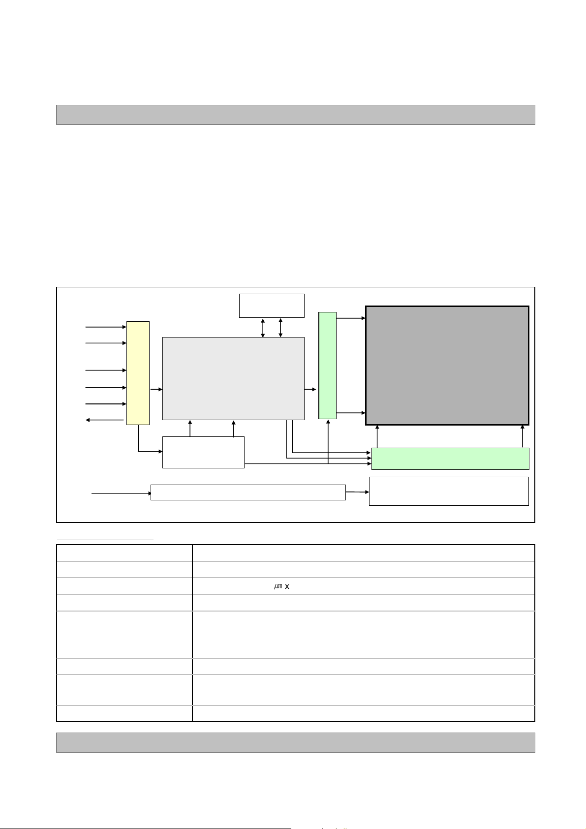
The LC320WXN is a Color Active Matrix Liquid Crystal Display with an integral
backlight system.
Direct (LED)
The matrix employs a-Si Thin Film Transistor as the active element.
Light Emitting Diode
It is a transmissive type display operating in the normally black mode. It has a 31.51 inch diagonally measured
ac t iv e d is p la y a re a w it h W X G A re s ol u ti on ( 7 68 v er t ic a l b y 1 3 66 h o ri zon t al pi x el a rra y) .
Each pixel is divided into Red, Green and Blue sub-pixels or dots which are arranged in vertical stripes.
Gray scale or the luminance of the sub-pixel color is determined with a 8-bit gray scale signal for each dot,
thus presenting a palette of more than 16.7M(true) colors.
It has been designed to apply the 8-bit 1-port LVDS interface.
It is intended to support LCD TV, PCTV where high brightness, super wide viewing angle, high color gamut,
high color depth and fast response time are important.
Lamp
+12.0V
LVDS
5pair
Select #9
DCR_Enable #10
VBR_EXT
+24.0V, VBR-A,
VBR-B, On/off
#28
#27VBR_OUT
CN1
(30pin)
General Features
EEPROM
SCL
SDA
Timing Controller
[LVDS Rx + ODC + DCR
+ SDRAM + Spread Spectrum
integrated]
Power Circuit
RGB
Block
CN2, Inverter (Master, 14Pin, High)
31.51 inches(800.4mm) diagonalActive Screen Size
760.0 mm(H) x 450.0 mm(V) x 48.0 mm(D) (Typ.)Outline Dimension
170.25 x 510.75㎛x RGBPixel Pitch
366 horiz. by 768 vert. pixels RGB stripe arrangementPixel Format
1
8bit, 16,7 M colorsColor Depth
10
00 cd/m2 (Center 1 point) (Typ.)Luminance, White
Viewing angle free ( R/L 178(Typ.), U/D 178(Typ.))Viewing Angle (CR>10)
Total Watt (Typ.) (Logic=3.5 W, Lamp= W [VBR-A= . V] )Power Consumption
80.5
6,150g(Typ.)Weight
Transmissive mode, normally blackDisplay Operating Mode
Hard coating(3H), anti-glare treatment of the front polarizer (Haze 13%)Surface Treatment
G1
Gate Driver Circuit
TFT - LCD Panel
(1366 × RGB × 768 pixels)
G768
S1 S1366
Source Driver Circuit
Back light Assembly (12EEFL)
3
77
3
Ver. 0.5
4 / 26
LC320WXN
Product Specification
2. Absolute Maximum Ratings
The following items are maximum values which, if exceeded, may cause faulty operation or damage to the
LCD module.
Table 1. ABSOLUTE MAXIMUM RATINGS
Value
Parameter Remark
Symbol
Unit
MaxMin
Power Input
Voltage
LCM
Backlight inverter
ON/OFF Control Voltage
Brightness Control Voltage
Operating Temperature
Storage Temperature
Operating Ambient Humidity
Storage Humidity
LCD
BL
ON/OFF
V
BR
OP
ST
OP
ST
+14.0-0.3V
+27.0-0.3V
+5.5-0.3V
+5.00
+500T
+60-20T
DC
V
DC
V
DC
V
DC
°C
°C
%RH9010H
%RH9010H
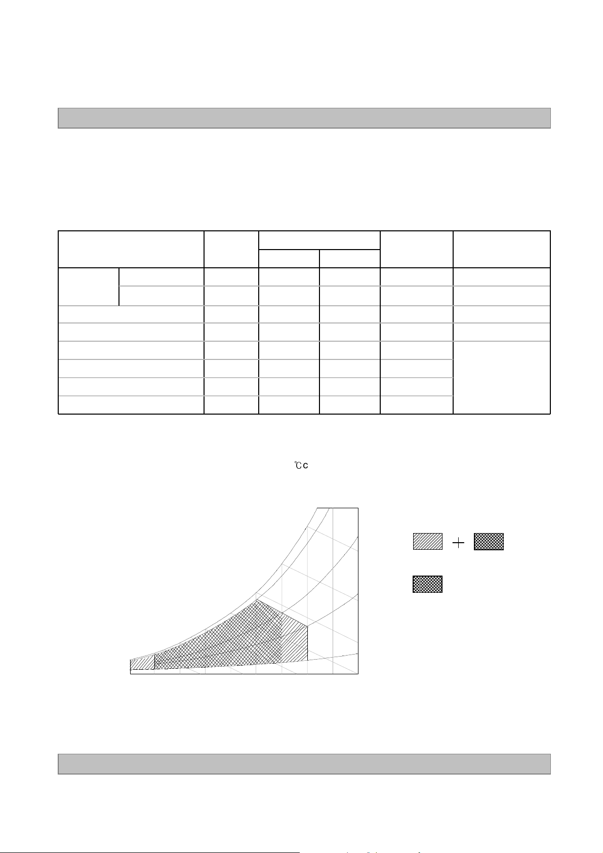
Notes : 1. Temperature and relative humidity range are shown in the figure below.
Wet bulb temperature should be 39 °C Max. and no condensation of water.
2. Gravity mura can be guaranteed under 40℃condition.
90%
60
60%
at 25 ± 2 °CV
Note 1,2
Ver. 0.5
Wet Bulb
Temperature [°C]
20
10
0
10 20 30 40 50 60 70 800-20
Dry Bulb Temperature [°C]
30
40
50
40%
10%
Storage
Operation
Humidity [(%)RH]
5 / 26
Product Specification
3. Electrical Specifications
3-1. Electrical Characteristics
It requires two power inputs. One is employed to power for the LCD circuit.
The other Is used for the EEFL backlight and inverter circuit.
Table 2. ELECTRICAL CHARACTERISTICS
LC320WXN
Parameter Symbol
Value
Circuit :
Power Input Voltage
Power Input Current
Power Consumption
Rush current
LCD
I
LCD
LCD
RUSH
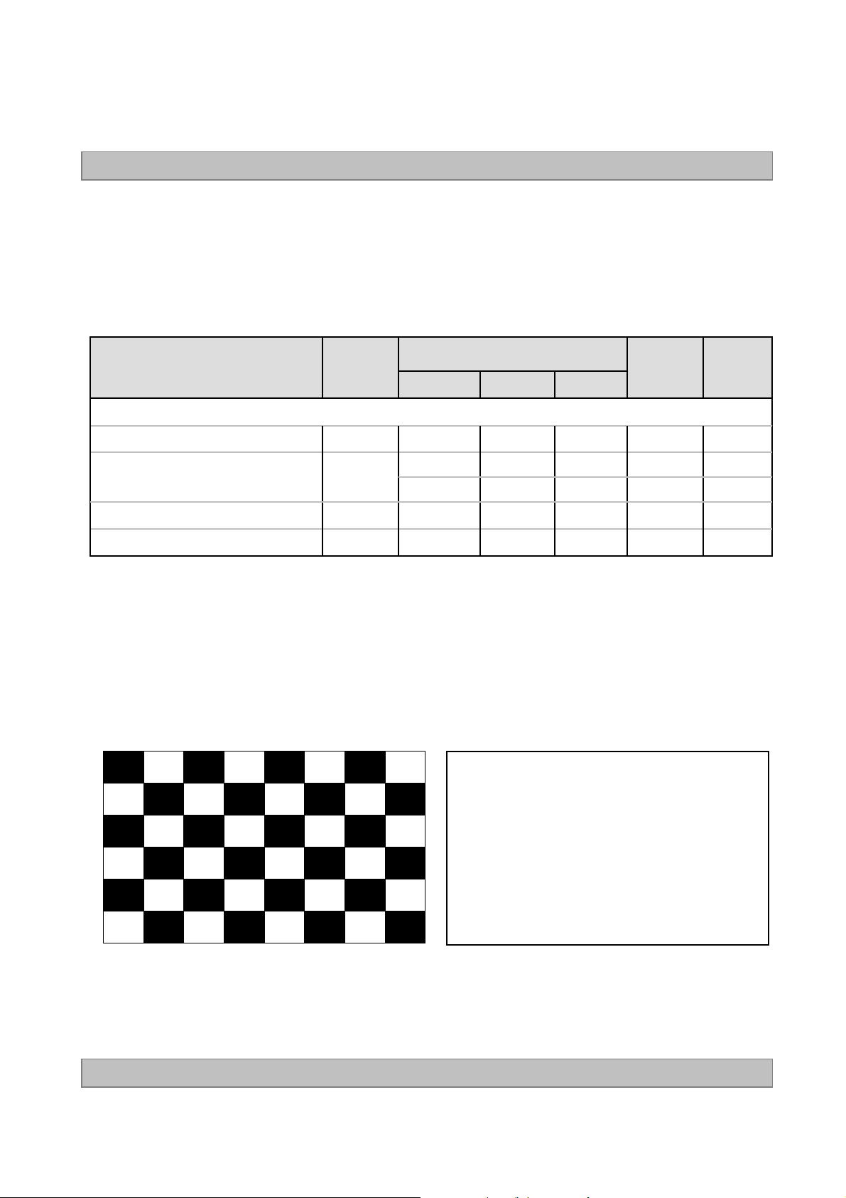
Notes : 1. The specified current and power consumption are under the V
condition whereas mosaic pattern(8 x 6) is displayed and fVis the frame frequency.
2. The current is specified at full white pattern.
3. The duration of rush current is about 2ms and rising time of power input is 1ms (min.).
White : 255 Gray
Black : 0 Gray
MaxTypMin
12.612.011.4V
=12.0V, 25 ± 2°C, fV=60Hz
LCD
V
DC
White : 255 Gray
NoteUnit
1mA384295-
2mA494380-
1Watt4.63.5-P
3A3.0--I
Ver. 0.5
Mosaic Pattern(8 x 6)
Full White pattern
6 / 26
Product Specification
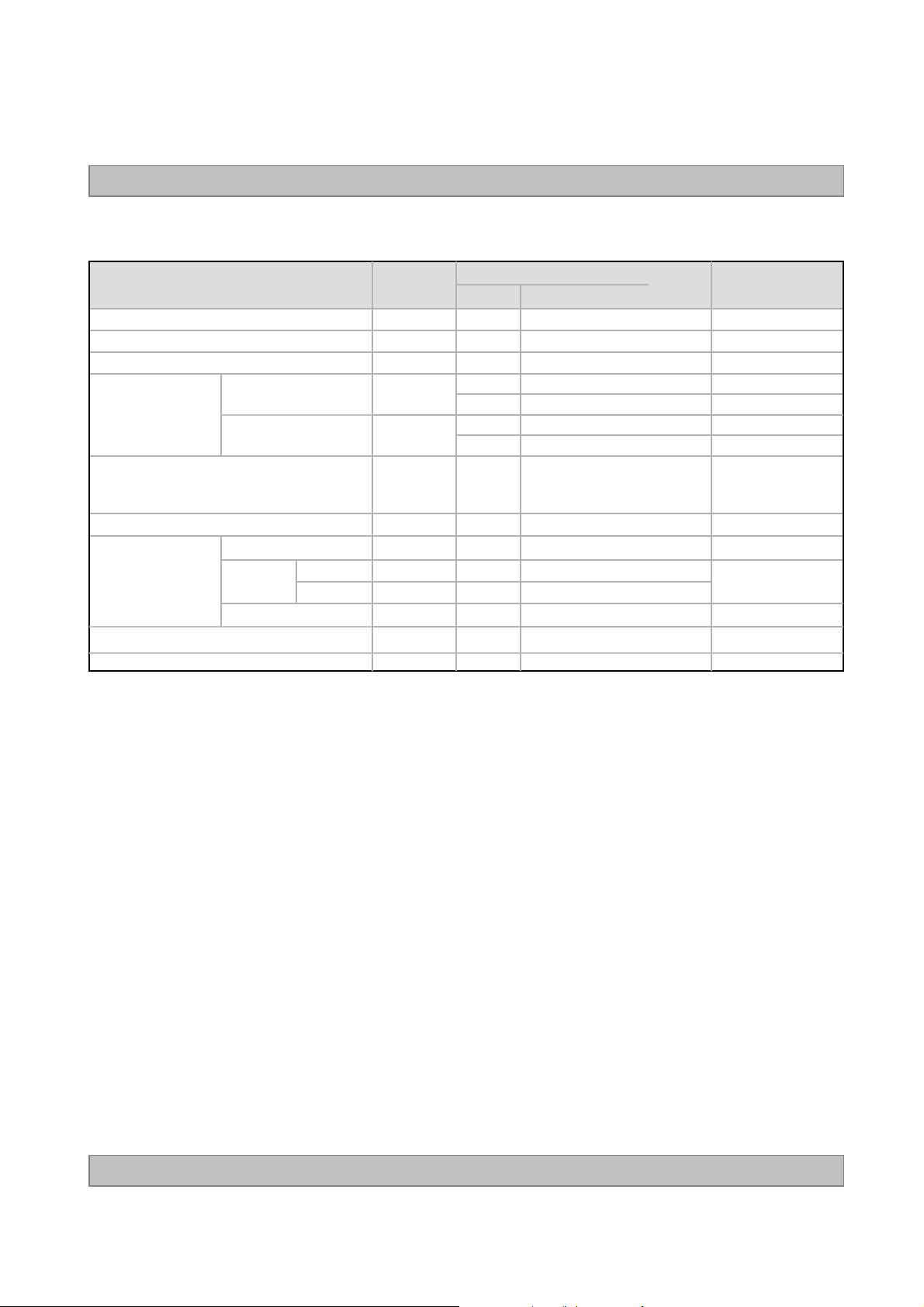
Table 3. ELECTRICAL CHARACTERISTICS (Continue)
LC320WXN
Parameter Symbol
Values
MaxTypMin
NotesUnit
Inverter :
Power Supply Input Voltage
Power Supply Input Voltage Ripple
Power Supply
Input Current
After Aging
Before Aging
Power Supply Input Current (In-Rush)
Power Consumption
Brightness Adjust
Input Voltage for
Control System
On/Off
Signals
Brightness Adjust
On
Off
IBL_A
IBL_B
VBR-A
VBR-B
3.5
77
Vdc25.224.022.8VBL
V
BR-A
V
BR-A
V
BR-A
V
BR-A
VBL= 22.8V
V
--Irush
6
.3
A
Vdc3.31.650.0
Vdc5.0-2.5V on
Vdc0.80.0-0.3V off
BR-B
V
BR-A
V
BR-A
1
1Vp-p0.5--
= 1.65V … 1A-
= 3.3V … 1A-
= 1.65V … 2A-
= 3.3V … 2A-
= 3.3V
= 1.65V
= 1.65V … 1W-PBL
3V3.3-0
Lamp:
Life Time
4Hrs50,000
Notes :
1. Electrical characteristics are determined after the unit has been ‘ON’ and stable for approximately 120
minutes at 25± 2°C. The specified current and power consumption are under the typical supply Input voltage
24Vand VBR (VBR-A : 1.65V & VBR-B :3.3V), it is total power consumption.
The ripple voltage of the power supply input voltage is under 0.5 Vp-p. LPL recommend Input Voltage is
24.0V ± 5%.
2. Electrical characteristics are determined within 30 minutes at 25± 2°C.
The specified currents are under the typical supply Input voltage 24V.
3. The brightness of the lamp after lighted for 5minutes is defined as 100%.
TS is the time required for the brightness of the center of the lamp to be not less than 95% at typical current.
The screen of LCD module may be partially dark by the time the brightness of lamp is stable after turn on.
4. Specified Values are for a single lamp which is aligned horizontally.
The life time is determined as the time which luminance of the lamp is 50% compared to that of initial value
at the typical lamp current (VBR-A : 1.65V & VBR-B :3.3V), on condition of continuous operating at 25± 2°C
5. The duration of rush current is about 20 ms.
Ver. 0.5
7 / 26
LC320WXN
Product Specification
3-2. Interface Connections
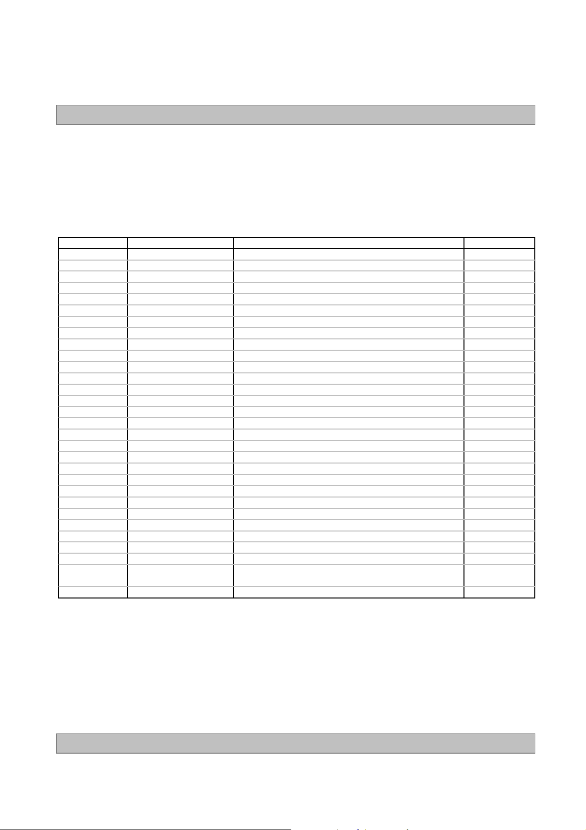
This LCD module employs two kinds of interface connection, a 30-pin connector is used for the module
electronics and One connectors(14-pin) are used for the integral backlight system.
3-2-1. LCD Module
- LCD Connector(CN1) : FI-X30SSL-HF (Manufactured by JAE) or Equivalent
- Mating Connector : FI-X30C2L (Manufactured by JAE) or Equivalent
Table 4. MODULE CONNECTOR(CN1) PIN CONFIGURATION
VLCD Power Supply +12.0V1
Power Supply +12.0VVLCD2
Power Supply +12.0VVLCD3
Power Supply +12.0VVLCD4
GroundGND5
GroundGND6
GroundGND7
GroundGND7
10
27
28
DCR Enable
Reserved29
Dynamic CR Enable ( ‘L ’ = Disable , ‘H’ = Enable )
GroundGND11
LVDS Receiver Signal(-)RA-12
LVDS Receiver Signal(+)RA+13
GroundGND14
LVDS Receiver Signal(-)RB-15
LVDS Receiver Signal(+)RB+16
GroundGND17
LVDS Receiver Signal(-)RC-18
LVDS Receiver Signal(+)RC+19
GroundGND20
LVDS Receiver Clock Signal(-)RCLK-21
LVDS Receiver Clock Signal(+)RCLK+22
GroundGND23
LVDS Receiver Signal(-)RD-24
LVDS Receiver Signal(+)RD+25
GroundGND26
VBR output fo rm LCD mo duleVBR_OUT
External VBR input from System to LCD moduleVBR_EXT
Low : Normal Operating
High : Interlace Free Mode
NoteDescriptionSymbolPin No.
1Select LVDS Data formatSelect9
2
3GroundGND30
Notes: 1. The pin no 9 is an option pin for DISM or LG format. ( VESA Format = “GND” / JEIDA Format =“VCC”)
Please refer to Appendix for further details.
2. The pin no 10 is an option pin for DCR Function ( Enable = “VCC” / Disable =“GND”)
3. The pin no 30 is LCD Test option.
LCM operates “AGP” (Auto Generation Pattern) or “NSB” (No Signal Black) is case that LVDS signals
are out of frequency or abnormal condition in spite of 12 volt power supply.
LPL recommends “NSB”. ( AGP : “VCC” or “OPEN” / NSB : “GND” )
4. All GND (ground) pins should be connected together, which should be also connected to the LCD
module’s metal frame.
5. All V
LCD
(power input) pins should be connected together.
6. Input Levels of LVDS signals are based on the IEA 664 Standard.
Ver. 0.5
8 / 26
Product Specification
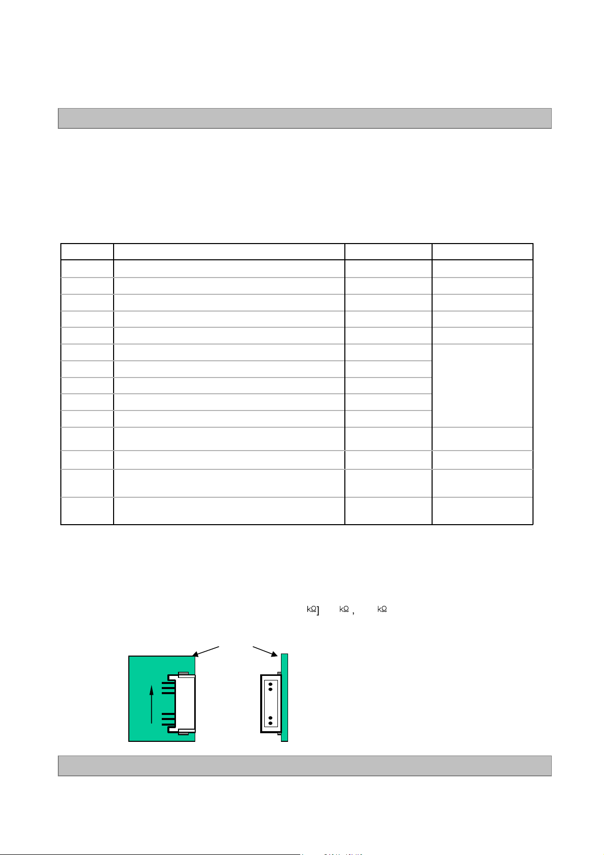
3-2-2. Backlight Inverter
Master
-Inverter Connector : 20022WR-14B1
(manufactured by Yeon-Ho) or Equivalent
- Mating Connector : PHR-14 or Equivalent
Table 7. INVERTER CONNECTOR PIN CONFIGULATION
1
2
3
4
5
6
7
8
9
10
GND
GND
GND
GND
GND
Power Supply +24.0VVBL
Power Supply +24.0VVBL
Power Supply +24.0VVBL
Power Supply +24.0VVBL
Power Supply +24.0VVBL
Backlight Ground
Backlight Ground
Backlight Ground
Backlight Ground
Backlight Ground
Master
VBL
VBL
VBL
VBL
VBL
GND
GND
GND
GND
GND
LC320WXN
NoteDescriptionSymbolPin No
1
11
12
13
14
ON/OFF
VBR-
Status
A
Burst dimming voltage
DC 0.0V ~ 3.3V
Normal : Upper 3.0V
Abnormal : Under 0.7V
Notes : 1. GND should be connected to the LCD module’s metal frame.
2. If Pin #1 is open, VBR-A = 1.65V. When apply over 1.65V( ~ 3.3V) continuously,
3
its luminance is increasing however lamp’s life time is decreasing.
It could be usable for boost up luminance when using DCR (=Dynamic contrast ratio) function only.
3. Minimum Brightness : VBR-B =0V Maximum Brightness : VBR-B = 3.3V
4. Even though Pin #14 is open, there is no effect on inverter operating, The output terminal of inverter.
5. Each impedance of pin #11,12 and 13 is 147[㏀], 38[㏀], 118[㏀]
◆◆◆◆ Rear view of LCM
PCB
14
…
1
…
On/Off0.0V ~ 5.0VV
VBR
3
2,
4Status
Ver. 0.5
9 / 26
LC320WXN
Product Specification
3-3. Signal Timing Specifications
Table 6 shows the signal timing required at the input of the LVDS transmitter. All of the interface signal
timings should be satisfied with the following specification for normal operation.
Table 6. TIMING TABLE for NTSC &PAL
CLK
HT
HV
-
H
WH
HBP
HFP
VT
VV
DCLK
Hsync
Period
Period
Horizontal Valid
Horizontal Blank
Frequency
Width
Horizontal Back Porch
Horizontal Front Porch
Period
Vertical Valid
HP-tHV
[ DE (Data Enable) Only ]
NoteUnitMaxTypMinSymbolITEM
ns15.813.812.5t
MHz8072.463-Frequency
t
192015281456t
136613661366t
t
162t
HP-tHV
5047.445f
-32-t
-5024t
-8040t
1063790776t
768768768t
CLK
t
CLK
KHz
t
CLK
t
HP
t
HP
t
HP
Hz636047f
t
HP
Hz-155t
t
HP
Vsync
Frequency
Width
Vertical Back Porch
Vertical Front Porch
-Vertical Blank
V
WV
VBP
VFP
VP-tVV
t
22t
VP-tVV
-5-t
-21t
Note :
1. The performance of the electro-optical characteristics may be influenced by variance of the vertical
refresh rate.
2. Above Timing Tables are only valid for DE Mode.
Ver. 0.5
Note 1)
PAL : 47~53Hz
NTSC : 57~63Hz
10 / 26
 Loading...