

Page 1

Q9T4-FP91G LCD Monitor Service Guide
Engineering Specification
Table of Contents
1. Introduction 3
2. Operational Specification 4
2.1 Power supply.................................................................................................................................4
2.2 Signal interface .............................................................................................................................4
2.3 Video performance........................................................................................................................5
2.4 Scan range.....................................................................................................................................6
2.5 Plug & Play DDC2B Support .......................................................................................................6
2.6 Support Timings............................................................................................................................6
3. Operational & Functional Specification 7
3.1 Video performance........................................................................................................................7
3.2 Brightness Adjustable Range........................................................................................................7
3.3 Acoustical Noise ...........................................................................................................................7
3.4 Environment..................................................................................................................................7
3.5 Transportation...............................................................................................................................8
3.6 Electrostatic Discharge Requirements...........................................................................................8
3.7 EMC..............................................................................................................................................8
3.8 Reliability......................................................................................................................................9
4. LCD Characteristics 9
4.1 The Physical definition & Technology summary of LCD panel...................................................9
4.2 Optical characteristics of LCD panel............................................................................................9
5. User Controls 10
5.1 User’s hardware control definition................................................................................................10
5.2 OSD control function definition....................................................................................................10
6. Mechanical Characteristics 11
6.1 Dimension.....................................................................................................................................11
6.2 W eight...........................................................................................................................................11
6.3 Plastic............................................................................................................................................11
6.4 Carton............................................................................................................................................12
1
Confidential
Page 2

Q9T4-FP91G LCD Monitor Service Guide
Engineering Specification
7. Pallet & Shipment 12
7.1 Container Specification.................................................................................................................12
7.2 Carton Specification......................................................................................................................12
Product:.................................................................................................................................12
Package:................................................................................................................................12
8. Certification 13
IEC60950 13
Appendix: Physical Dimension Front View and Side view 14
2
Confidential
Page 3
Q9T4-FP91G LCD Monitor Service Guide
N
Engineering Specification
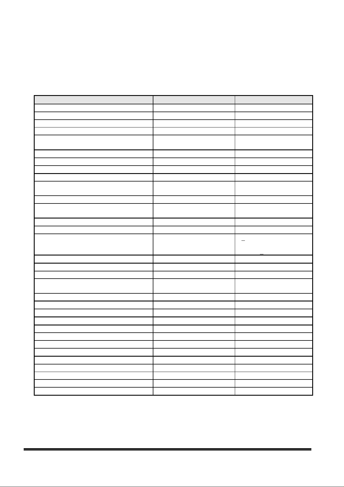
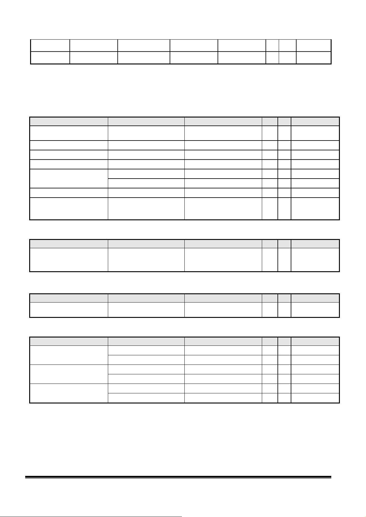
1. Introduction
This specification describes Q9T4, which is a 19.0” analog/digital interface color TFT LCD monitor without
audio. The monitor supports up to 1280x1024 pixel resolution and refresh rate of 75 Hz. The independent 6 bits
R, G, B colors are capable of displaying 262K colors (scaler dithering output 16.2M colors). In addition,
(typ.)
Panel spec.
With 15-pin D-sub connector
With 24-pin DVI-D connector
scaler dithering output 16.2M
colors
At CCFL 7mA & R/G/B
saturated condition
90-264 Volts, 47-63 Hz.
1W in power off preferred
<
mode, 120V
2W, 240V
<
Green/Amber/Non
8 languages
6 buttons including 1 monitor
power on/off control button.
“iKey” function
DDC2B only
From -5 to +20 degree
dithering function is supported. The features summary is shown below,
*All panel spec. in C201 definition depends on the variance of panel source.
Feature items Specifications Remark
Panel supplier & module name
Screen diagonal 19.0” (480mm) 376.32(H) x 301.056(V)
Display Format SXGA / 1280 (H) x 1024 (V)
Pixel Pitch 0.294 mm x 0.294 mm per one triad
Viewing Angle (@ Contrast Ratio = 10)
Analog interface with Scaling supported
DVI interface with Scaling supported
Video interface with Scaling supported No
Max resolution mode supported 1280 x 1024 @ 75Hz
umber of Display Colors supported
Contrast Ratio
Luminance
AC power input
DC power input (with AC power adapter) No
DPMS supported
LED indicator for power status showed
OSD for control & information supported
Multi-language supported for OSD
Buttons control supported
Flywheel control supported No
Scaling function supported
Auto adjustment function supported
DDC function supported (EDID ver. 1.3)
Audio speakers supported
Audio Jack (input connector) supported
Earphone Jack (input connector) supported
Microphone function supported No
Mechanical Tilt base design
VESA wall mounting design
Mechanical Rotate design No
Mechanical Lift base design No
Kensington compatible lock design
AUO M190EN04 V.2
R/L: 70/70 degrees (typ.)
and U/D: 70/65 degrees (typ.)
Yes
Yes
262K colors
450:1 (typ.)
250 cd/m
2
Yes
Yes
Yes
Yes
Yes
Yes
Yes
Yes
Yes
No
No
No
Yes
Yes
Yes
3
Confidential
Page 4
Q9T4-FP91G LCD Monitor Service Guide
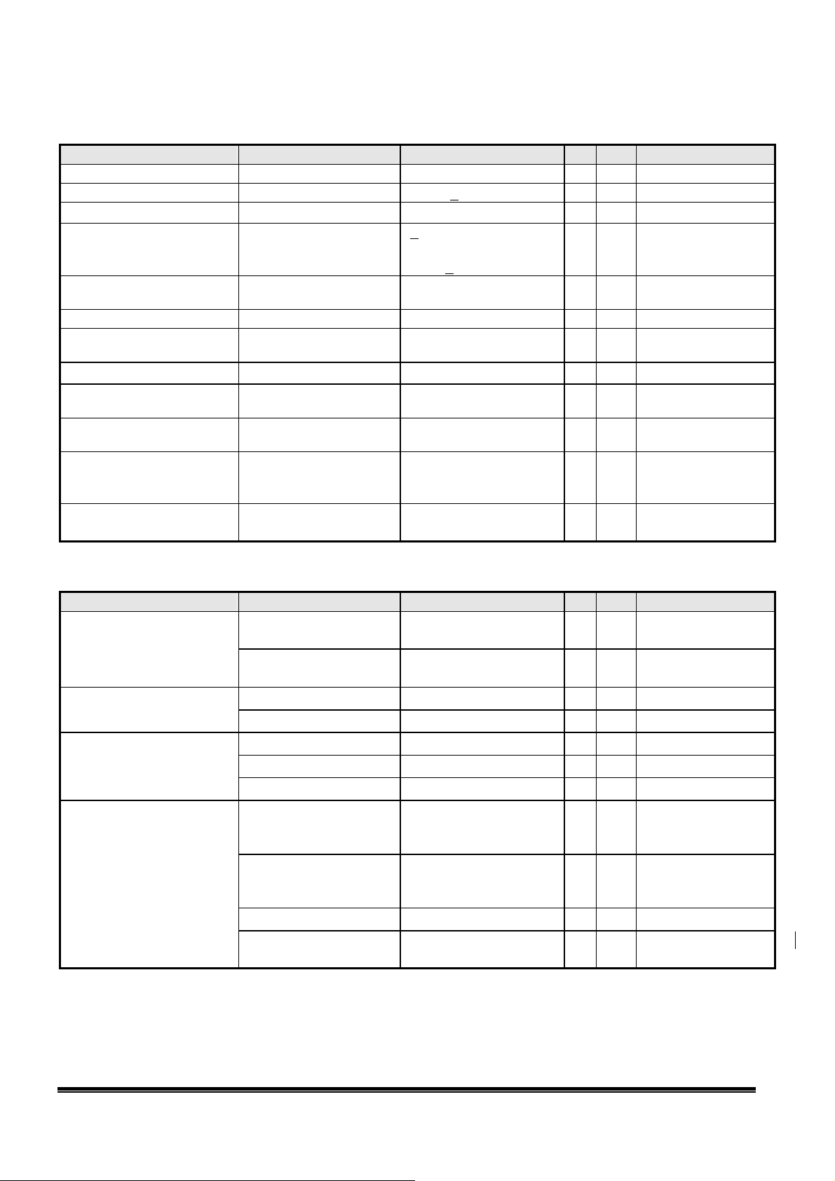
2. Operational Specification
2.1 Power supply
Item Condition Spec OK N.A Remark
Input Voltage range
Input Current range
Power Consumption
DPMS
Inrush Current
Earth Leakage Current
Hi-Pot
Power Line Transient
CCFL operation range
Universal input full range 90~264VAC /47~63Hz
90 ~ 264VAC < 2.0 Arms
Normal “On” operation
DPMS “Off” state
110 VAC
220 VAC
264 VAC/50Hz < 3.5 mA
1. 1500VAC, 1 sec
2. Ground test: 30A, 1sec
IEC1000-4-4 1KV √
IEC1000-4-5 (Surge)
90 ~ 264VAC 3.0 mA ~7.5mA
Engineering Specification
< 40 W (w/o speaker)
<
1 W in power preferred
mode, 120V
2 W, 240V
<
< 30 A (peak)
< 60 A (peak)
Without damage
< 0.1 ohm
Common: 2KV,
Differential: 1KV
√
√
LED: Green
√
LED: Amber
√
Cold-start
√
√
(on-line test)
√
√
√
(in-lab test)
Depends on panel
source
CCFL Frequency
Power cord
2.2 Signal interface
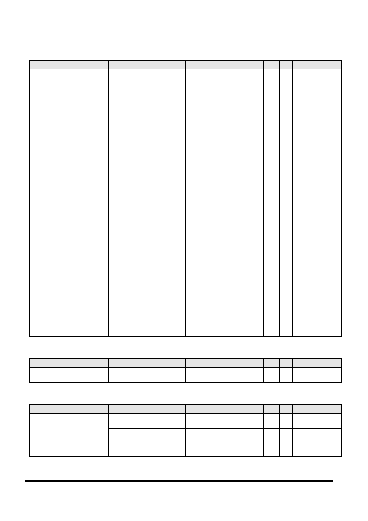
Item Condition Spec OK N.A Remark
Signal Cable
Pin assignment
Sync input
90 ~ 264VAC 40KHz ~ 80KHz
15-pin D-Sub
24-pin DVI-D
15-pin D-sub connector
24-pin DVI-D connector
Signal type
Level
Impedance
Signal type
Level
Impedance
Sync Pulse Width (SPW)
Logic High: 2.4V ~ 5.5V
Logic Low: 0V ~ 0.5V
Color: Black
Length: 1500
Color: Black
Length: 1500
Color: Black
Length: 2000
See Note-1
See Note-2
Separate analog R/G/B
700 mV (peak to peak)
75 Ohms +/- 1.5 Ohms
Separate H/V-sync
Composite H/V-sync
(Positive/Negative)
(TTL level)
Minimum 2.2K
0.7μs < H-SPW
1H < V-SPW
+/- 50 mm
+/-
30 mm
+/-
50 mm
Ω(pull down)
√
√
√
√
√
√
√
√
√
√
√
√
√
Depends on panel
source
For 15-pin D-sub
For 24-pin DVI-D
For 15-pin D-sub
Video input
For 15-pin D-sub
Refer to VESA VSIS
Standard V1R1
10KΩ for application
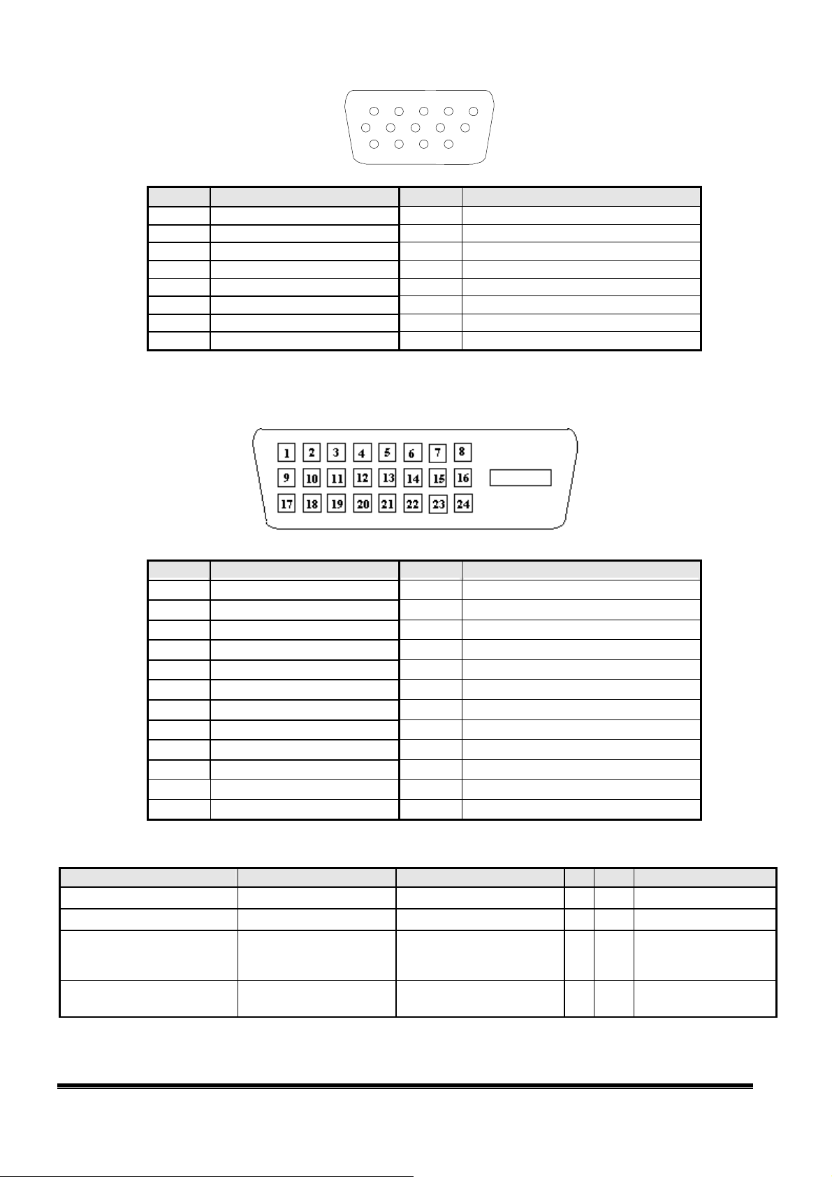
Note-1: The pin assignment of 15-pin D-sub connector is as below,
4
Confidential
Page 5
Q9T4-FP91G LCD Monitor Service Guide
1 5
Engineering Specification
6
11 15
10
Pin Signal Assignment Pin Signal Assignment
1 Red video 9 PC5V (+5 volt power)
2 Green video 10 Sync Ground
3 Blue video 11 Ground
4 Ground 12 SDA
5 Cable Detected 13 H-Sync (or H+V)
6 Red Ground 14 V-sync
7 Green Ground 15 SCL
8 Blue Ground
Note-2: The pin assignment of 24-pin DVI-D connector is as below,
Pin Signal Assignment Pin Signal Assignment
1 TMDS RX2- 13 Floating
2 TMDS RX2+ 14 +5V Power
3 TMDS Ground 15 Ground
4 Floating 16 Hot Plug Detect
5 Floating 17 TMDS RX06 DDC Clock 18 TMDS RX0+
7 DDC Data 19 TMDS Ground
8 Floating 20 Floating
9 TMDS RX1- 21 Floating
10 TMDS RX1+ 22 TMDS Ground
11 TMDS Ground 23 TMDS Clock+
12 Floating 24 TMDS Clock-
2.3 Video performance
Item Condition Spec OK N.A Remark
Max. support Pixel rate
Max. Resolution
< 6.25 ns
Rise time + Fall time
Settling Time after
overshoot /undershoot
5
Confidential
< 5% final full-scale value
135 MHz
1280 x 1024
(50% of minimum pixel
clock period)
√
√
√
√
1280 x 1024 @ 75Hz
(max. support timing)
Refer to VESA VSIS
Standard V1R1
Page 6
Q9T4-FP91G LCD Monitor Service Guide
OS
OS
OS
VES
VES
VES
VES
VES
VES
VES
VES
VES
SU
SU
VES
< 12% of step function
Overshoot/Undershoot
2.4 Scan range
Item Condition Spec OK N.A Remark
Horizontal
Vertical
2.5 Plug & Play DDC2B Support
Item Condition Spec OK N.A Remark
DDC channel type
EDID
2.6 Support Timings
Engineering Specification
voltage level over the full
voltage range
31 ~ 81 KHz
56 ~ 76 Hz
DDC2B
Version 1.3
√
√
√
√
√
Refer to VESA VSIS
Standard V1R1
Without Frame buffer
Refer to Q9T4 S/W
spec. document to see
the detailed EDID data
definition.
Input Timing
Resolution
640x350 31.47(P) 70.08(N) 25.17 1280x943
720x400 31.47(N) 70.08(P) 28.32 1280x1024
640x480 31.47(N) 60.00(N) 25.18 1280x1024
640x480 35.00(N) 67.00(N) 30.24 1280x1024
640x480 37.86(N) 72.80(N) 31.5 1280x1024
640x480 37.50(N) 75.00(N) 31.5 1280x1024
800x600 37.88(P) 60.32(P) 40.00 1280x1024
800x600 48.08(P) 72.19(P) 50.00 1280x1024
800x600 46.86(P) 75.00(P) 49.50 1280x1024
832X624 49.72(N) 74.55(N) 57.29 1280x1024
1024x768 48.36(N) 60.00(N) 65.00 1280x1024
1024x768 56.48(N) 70.10(N) 75.00 1280x1024
1024x768 60.02(P) 75.00(P) 78.75 1280x1024
1024X768 60.24(N) 74.93(N) 80.00 1280x1024
1152x864 67.50(P) 75.00(P) 108.00 1280x1024
1152x870 68.68(N) 75.06(N) 100.00 1280x1024
1152x900 61.80(N) 66.00(N) 94.50 1280x1024
1152x900 71.81(N) 76.14(N) 108.00 1280x1024
1280x1024 64.00(P) 60.00(P) 108.00 1280x1024
1280x1024 75.83(N) 71.53(N) 128.00 1280x1024
Horizontal Vertical Dot Clock Actual display
Actual Output
OK N.A
√
√
√
√
√
√
√
√
√
√
√
√
√
√
√
√
√
√
√
√
Remark
D
D
D
Macintosh
A
A
A
A
A
Macintosh
A
A
A
Macintosh
A
Macintosh
N 66
N
A
IBM1
6
Confidential
Page 7
Q9T4-FP91G LCD Monitor Service Guide
VES
S
Engineering Specification
1280x1024 80.00(P) 75.00(P) 135.00 1280x1024
1280x1024 81.18(N) 76.16(N) 135.09 1280x1024
Note-3: “P”, “N” stands for “Positive”, “Negative” polarity of incoming H-sync/V-sync (input timing).
√
√
3. Operational & Functional Specification
3.1 Video performance
Item Condition Spec OK N.A Remark
Resolution
Contrast ratio
Brightness
Response time
Viewing angle
CIE coordinate of White
Display colors
Any input resolution modes
which are under 1280 x 1024
450:1 (typ.)
At R/G/B saturated condition 250 cd/m2 (typ.) @ 7mA
Rising + Falling time 12 ms (typ.)
At Contrast ratio = 10 R/L: 70/70 degrees (typ.)
At Contrast ratio = 10 U/D: 70/65 degrees (typ.)
(0.31, 0.33) +/- (0.03, 0.03)
262K colors
1280 x 1024
√
√
√
√
√
√
√
√
3.2 Brightness Adjustable Range
Item Condition Spec OK N.A Remark
Brightness adjustable range
At default contrast level
(saturate point) & Full-white
color pattern
(Max. brightness value –
Min. brightness value)
≧ 100 cd/㎡
√
A
PARC2
scaler dithering
output 16.2M
colors
3.3 Acoustical Noise
Item Condition Spec OK N.A Remark
Acoustical Noise
3.4 Environment
Item Condition Spec OK N.A Remark
Temperature
Humidity
Altitude
At 1 meter distance
& “Audio” function disabled
Operating
Non-operating
Operating 10 ~ 90%
Non-operating 10 ~ 90%
Operating 0~3048m (10,000ft)
Non-operating 0~12,192m (40,000ft)
≦ 40 dB/A
0 ~ +40 ℃
-20 ~ +60 ℃
√
√
√
Non-condensing
√
Non-condensing
√
Without packing
√
With packing
√
7
Confidential
Page 8
Q9T4-FP91G LCD Monitor Service Guide
p
3.5 Transportation
Item Condition Spec OK N.A Remark
(1) Vibration
(2) Unpackaged Vibration
(3) Drop
(4) Shock
Package, Non-Operating
Unpackaged, Non-Operating
Package, Non-Operating
Wooden package,
Non-Operating
Engineering Specification
(1) Sine wave
5~200Hz 1.5G, 1 octave/min,
15 min dwell on each resonant
frequency, all primary axis,
one sweep (30 min minimum)
er orientation, total of 90+
min.
(2) Random
5 ~100 Hz, 0 dB/Oct. 0.015
2
/Hz
g
100 ~200 Hz, -6 dB/Oct.
200 Hz, 0.0038 g
Equivalent to 1.47 Grms, All
primary axis, 20 min perorientation, total is 60 min.
(3) Procedure:
Confirmed sample with
appearance and function ready
before testing then compare
with after test record as
brightness, uniformity and
contrast ratio. Perform
random vibration after
sine-wave vibration test.
Test Spectrum:
20 Hz 0.0185(g2/Hz)
200Hz 0.0185(g2/Hz)
Duration : 5 Minutes
Axis : 3 axis ( Horizontal
and Vertical axis ,Z axis)
91 cm Height (MP stage)
(1 corner, 3 edges, 6 faces)
Waveform: half sine
Faces: 6 sides/ per orientation
3 shocks.
Duration: <3ms
Velocity accelerate: 75g
2
/Hz
√
√
√
√
3.6 Electrostatic Discharge Requirements
Item Condition Spec OK N.A Remark
Electrostatic Discharge
IEC801-2 standard
Contact: 8KV
Air: 15KV
√
3.7 EMC
Item Condition Spec OK N.A Remark
Electric
TCO03
Magnetic
EMI
8
Confidential
FCC part 15J class B
Band 1 < 10 V/m
Band 2 < 1 V/m
Band 1 < 200nT
Band 2 < 25nT
After Mass production under
√
√
√
Page 9
Q9T4-FP91G LCD Monitor Service Guide
Engineering Specification
EN55022 class B
1dBuv for constant measure.
Besides DNSF and VCCI
class-2 are optional.
3.8 Reliability
Item Condition Spec OK N.A Remark
MTBF Prediction
CCFL Life time
Refer to MIL-217F > 60,000 Hours
At 25±2℃, under 7.0mA
50,000 Hours (typ.)
√
√
Excluding CCFL
Note-4: CCFL lifetime is determined as the time at which brightness of lamp is 50%. The typical lifetime of
CCFL is on the condition at 7.0±0.5mA lamp current.
4. LCD Characteristics
4.1 The Physical definition & Technology summary of LCD panel
Item Condition Spec OK N.A Remark
LCD Panel Supplier
Panel type of Supplier
Screen Diagonal
Display area
Physical Size
Weight
Unit=mm 376.32(H) x 301.056(V)
Unit=mm 396(H) x 324(V) x 18(D) (typ.)
Unit=gram 2700 (typ.)
Technology
Pixel pitch
Unit=mm 0.294 x 0.294
Pixel arrangement
Display mode
Support color
TN type
R/G/B vertical stripe
262K colors (scaler dithering output
AUO
M190EN04 V.2
480mm(19.0”)
Normally white
16.2M colors)
√
√
√
√
√
√
√
√
√
√
√
See Note-4
Per one triad
4.2 Optical characteristics of LCD panel
Item Unit Conditions Min. Typ. Max. Remark
[degree]
Viewing Angle
[degree]
[degree]
[degree]
Contrast ratio
[msec] Rising Time - 3.6 6.3
Response Time
[msec] Falling Time - 8.4 14.7
[msec] Rising + Falling - 12 21
Color / Chromaticity
Coordinates (CIE)
Color Coordinates (CIE) White
Luminance Uniformity
9
Confidential
[%] 9 points measurement
Horizontal (Right)
CR = 10 (Left)
Vertical (Up)
CR = 10 (Down)
Normal Direction
Red x 0.604 0.634 0.664
Red y 0.324 0.354 0.384
Green x 0.27 0.3 0.3
Green y 0.585 0.615 0.645
Blue x 0.108 0.138 0.168
Blue y 0.047 0.077 0.107
White x 0.28 0.31 0.34
White y 0.30 0.33 0.36
65
65
65
60
250 450
70 75 -
70
70
70
65
-
-
-
-
Page 10
Q9T4-FP91G LCD Monitor Service Guide
Engineering Specification
White Luminance @ CCFL
7.5mA (center)
Crosstalk (in 75Hz)
* The test methods for the above items’ definition, please refer to the relative panel specification.
[cd/m2]
[%]
200 250 -
1.5
5. User Controls
5.1 User’s hardware control definition
Item Condition Spec OK N.A Remark
Power button
Enter button
Right/Inc. button
Left/Dec. button
Exit /Volume or Input Select
button
iKey button
Mode button
Mute button
√
√
√
√
√
√
√
√
5.2 OSD control function definition
Item Condition Spec OK N.A Remark
Auto Adjust
Brightness
Contrast
Horizontal Position
Vertical Position
Pixel Clock
Phase
Color
OSD Position
OSD Time
Language
Recall
Mode
Input Select
Sharpness
Auto-Geometry
Bluish
Reddish
Normal
: Separate R/G/B adjustment
User
OSD Horizontal position
OSD Vertical position
From 5 sec to 60 sec
8 languages
Color recall
Recall All
D-sub
DVI
√
√
√
√
√
√
√
√
√
√
√
√
√
√
√
10
Confidential
Page 11
Q9T4-FP91G LCD Monitor Service Guide
Engineering Specification
Display Information
Volume
Mute
Hot key for Brightness
Hot key for Contrast
Hot key for Volume
Hot key for Input Select
Hot key for Mode
* The detailed firmware functions’ specification, please refer to C212 S/W spec. document.
For input timing
√
√
√
√
6. Mechanical Characteristics
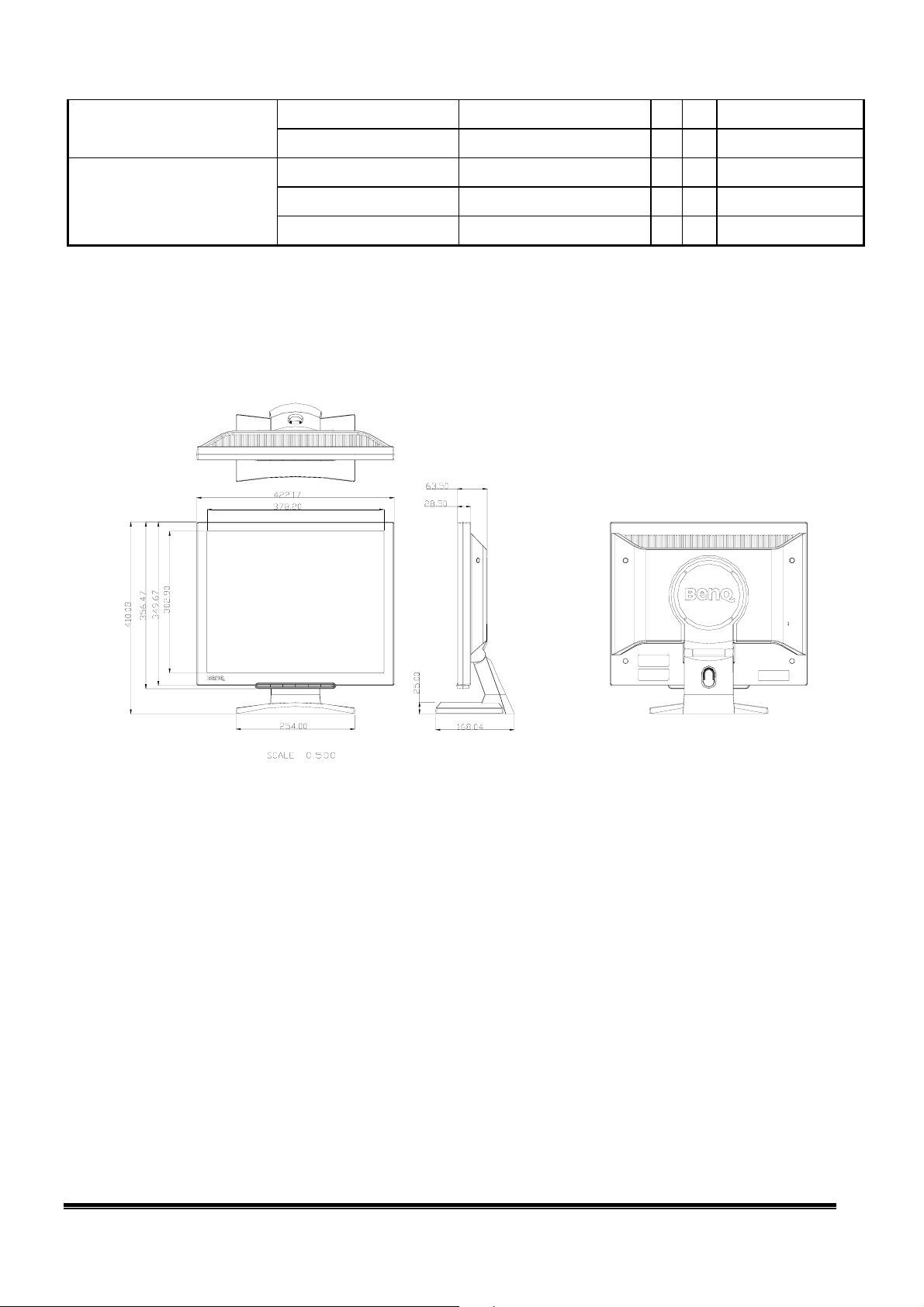
6.1 Dimension
Item Condition Spec OK N.A Remark
Bezel opening
Monitor without Stand
Monitor with Stand
Carton Box (outside)
Tilt and Swivel range
L x W x H mm
L x W x H mm
L x W x H mm
378.2 x 302.9 mm
356.5*422.2*63.5mm
410.1*422.2*168 mm
495 x 491x 157mm
Tilt: -5 ~ +20 degree
Swivel: 0 degrees
√
√
√
√
√
√
√
√
√
6.2 Weight
Item Condition Spec OK N.A Remark
Monitor (Net)
Monitor with packing
6.3 Plastic
Item Condition Spec OK N.A Remark
Flammability
Heat deflection To
UV stability
Resin
Texture
Color
(Gross)
ABS
ABS
(VW55/VE0856/D350)
5.1 Kg
6.8 Kg
94-HB
65 ℃
Delta E < 8.0
MPRII:
MT-11020
BCS-Y5003A
ABS
√
√
√
√
√
√
√
√
Bezel texture
MT-11010
Bezel painting
T8020C
11
Confidential
Page 12
Q9T4-FP91G LCD Monitor Service Guide
6.4 Carton
Item Condition Spec OK N.A Remark
Color
Material
Compression strength
Burst Strength
Stacked quantity
7. Pallet & Shipment
7.1 Container Specification
Quantity of products
Stowing Type Container
(sets)
(Every container)
Engineering Specification
Kraft
C Flute
396 KGF
(sets)
2
16 KGF/cm
13 Layers
Quantity of Products
(Every Pallet)
√
√
√
√
√
Quantity of pallet
(sets)
(Every Container)
With pallet
Without pallet
7.2 Carton Specification
Product:
Net Weight (Kg) Gross Weight (Kg)
Package:
20'
40'
20'
40'
5.1Kg 6.8Kg 356.5*422.2*63.5mm 410.1*422.2*168 mm
Carton Interior Dimension (mm)
L*W*H
485 x 481 x 139 495 x 491x 157
600 Pallet A: 60 Pallet A: 10
1440 Pallet A: 60 Pallet A: 24
600
1440
X X
Dimension w/o Base
L*W*H (mm)
Carton External Dimension (mm)
X X
X X
X X
Dimension w/ Base
L*W*H (mm)
L*W*H
12
Confidential
Page 13
Q9T4-FP91G LCD Monitor Service Guide
8. Certification
Item Condition Spec OK N.A Remark
Green design
Engineering Specification
API Doc. 715-C49
√
ISO14000
Requirement
Environment
PC-Monitor
Blue Angel German Standard
E-2000 Switzerland
EPA USA Standard
TCO’99
TCO’03
Green Mark
Microsoft Windows PC98/99
DPMS VESA
DDC 2B Version 1.3
USB External
UL (USA) UL60950 3rd edition
CSA (Canada) CAN/CSA-C22.2 No. 60950
Nordic / D.N.S.F EN60950
FIMKO EN60950
CE Mark 73/23/EEC
IEC60950
√
√
√
√
√
√
√
√
√
√
√
√
√
√
√
√
Safety
EMC
X- Ray Requirement
EN60950
CB
TUV/GS
CCC (China)
GOST EN60950
SASO
CE Mark 89/336/EEC
FCC (USA) FCC Part 15 B
EN60950
EN60950 /
EK1-ITB 2000:2003
√
√
√
√
√
√
√
√
EN55022 Class B
√
CISPR 22 Class B
VCCI (Japan) VCCI Class B
BSMI (Taiwan) CNS 13438
C-Tick (Australia) AS/ NZS CISPR22
DHHS (21 CFR) USA X- Ray Standard
√
√
√
√
√
13
Confidential
Page 14
Q9T4-FP91G LCD Monitor Service Guide
DNHW
Engineering Specification
√
PTB German X- Ray standard
TUV / Ergo
Ergonomics
ISO 13406-2
prEN50279
Appendix: Physical Dimension Front View and Side view
Fig. 1 Physical Dimension Front View and Side view
√
√
√
√
14
Confidential
Page 15
Q9T4-FP91G LCD Monitor Service Guide
N
Q9T4 TROUBLE SHOOTING GUIDE
1. No Display or display is unstable
Interface Board -
Y
N
Y N
o picture or picture
unstable
Power off?
Does cable plug in
connector?
Is power stable?
N
Trouble Shooting
Turn on power.
Plug all wires then turn on power again.
Check power BD.
Y
N
Is LED light green?
Y N
Does DVI signal work?
Y
+
+
Check control BD.
Check (U1) DDC data.
N
Is LED status normal?
Check MCU (U4) or replace it.
1
Confidential
Page 16

Q9T4-FP91G LCD Monitor Service Guide
Y N
Trouble Shooting
Does crystal work
correctly?
Y N
Is LED status normal?
Y
N
Does LVDS cable
connect to panel?
Y
Check Panel or replace it.
Check crystal (Y2) CKT or replace it.
Replace interface BD or check scaler TSU56AL (U2).
Plug LVDS cable again or replace it.
2
Confidential
Page 17

Q9T4-FP91G LCD Monitor Service Guide
2. BUTTON function
Control board -
N
OSD doesn’t work.
Trouble Shooting
Is control BD working?
Y N
Is button switch
working?
Y
N
Check Interface BD
L7~L12, R55~R60,
R41, R42, RN1, RN2
OK?
Check Interface BD.
Y
Plug control BD then retry.
Replace control BD then
Replace component then
3
Confidential
Page 18

Q9T4-FP91G LCD Monitor Service Guide
3. OSD function
Trouble Shooting
OSD doesn’t work
N
Is control BD working?
Y
Check Interface BD
Replace control BD
4
Confidential
Page 19

Q9T4-FP91G LCD Monitor Service Guide
4. Power Board
Backlig ht didn 't shine
Trouble Shooting
Check IC801
Plug CN701 again or
checking I/F BD
Plug CN601 again or
checking PW BD
Insert the m a gain
Y
N
N
N
IC801 PIN 9 IS
PWM existed?
Turn on level existed?
Check CN801~CN804
was pluged properly?
IC801,Q805,Q812
12~16V?
N
(BLT_ADJ)
Y
(BLT_ON)
Y
Y
Replace
Y
LED shined?
N
Y
3.3V existed? IS I/F board connected?
Y
Replace new fuse
N
Y
Check IC701 OK?
N
Checking F601
Broke?
N
Check IC601 Vcc
existed?
Y
Y
Replace IC701
Replace new fuse
Replace
IC601,Q602,
N
Replace new fuse
N
Replace IC602,
IC702,D701 or
check I/F BD
5
Confidential
Page 20

Q9T4-FP91G LCD Monitor Service Guide
Alignment Procedure
Table of Contents
1. ALIGNMENT PROCEDURE (FOR FUNCTION ADJUSTMENT)......................................................................................................2
The list of necessary alignment for a LCD monitor ...................................................................................................................2
A. Preparation............................................................................................................................................................................2
B. Geometry adjustment & checking (for preset timing modes).................................................................................................2
C. ADC calibration (White Balance)..........................................................................................................................................2
D. Color temperature measurement...........................................................................................................................................3
E. Writing EDID data into monitor............................................................................................................................................3
F. Command definition...............................................................................................................................................................3
2. EEPROM MAPPING.................................................................................................................................................................6
3. WIRE DRESSING.......................................................................................................................................................................7
- ASSEMBLY NOTE........................................................................................................................................................................7
4. ADD GLUE ..............................................................................................................................................................................10
1
Confidential
Page 21

Q9T4-FP91G LCD Monitor Service Guide
Alignment Procedure
1. Alignment procedure (for function adjustment)
The list of necessary alignment for a LCD monitor
Items Description Remark
1 Geometry adjustment & checking For Preset timing modes
2 ADC calibration (White balance adjustment) UVGA7 (1024x768/75Hz)
3 Color temperature measurement C1/Bluish, C2/Reddish & C3/Normal
4 Writing EDID data into monitor Analog/DVI-D
A. Preparation
1. Setup input timing to any preset modes or patterns.
2. Enter factory mode (press “Exit” & “Enter” & “Power” buttons at the same time to turn on monitor).
3. Press “iKey” into “Burn In Mode” tag and select “On” to enable burn-in mode.
4. Power off the monitor, remove the input source and then power on again.
5. Setup unit and keep it warm up for at least 30 minutes.
B. Geometry adjustment & checking (for preset timing modes)
1. Enter factory mode (press “Exit” & “Enter” & “Power” buttons at the same time to turn on monitor).
2. Select timing mode from figure-1 and input full screen display pattern to monitor.
3. Select “Auto Adjust” to run “AUTO” function for geometry adjustment.
4. Check if the position, phase and clock of the image are correct to make sure controlled functions and performance are
O.K..
5. Select “Recall All ” to erase user settings.
6. Turn off the monitor power.
7. Turn on the monitor power again to check if monitor’s image settings are O.K. and with following settings.
CONTRAST = 50
BRIGHTNESS = 90
COLOR = Normal (default setting)
OSD time = 20
Figure-1: Preset Timing modes list
Input Timing Actual Output
Resolution
720x400 31.47(N) 70.08(P) 28.32 1280x1024 √ DOS
800x600 46.87(P) 75.00(P) 49.5 1280x1024 √ VESA
1024x768 48.36(N) 60.00(N) 65.00 1280x1024 √ VESA
1024x768 60.02(P) 75.00(P) 78.75 1280x1024 √ VESA
1152x870 68.68(N) 75.06(N) 100.00 1280x1024 √ Mac
1152x900 71.81(N) 76.14(N) 108.00
1280x1024 80.00(P) 75.00(P) 135.00 1280x1024 √ VESA
1280x1024 81.18(N) 76.16(N) 135.09 1280x1024 √ SUN
Horizontal
Frequency (KHz)
C. ADC calibration (White Balance)
~~Analog only, it is not required for DVI-D input source
Vertical
Frequency (Hz)
Dot Clock
Frequency (MHz)
Actual display
Resolution
1280x1024 √ VESA
OK N.A Remark
2
Confidential
Page 22

Q9T4-FP91G LCD Monitor Service Guide
Alignment Procedure
1. Setup input timing UVGA7 (1024x768/75Hz), pattern 42 (5-Mosaic pattern with white color block) with Analog
signals from Chroma video pattern generator. (it depends on Scaler IC supplier’s recommendation)
2. Enter factory mode (press “Exit” & “Enter” & “Power” buttons at the same time to turn on monitor).
3. Press “iKey” into “Burn In Mode” tag and select “On” to enable burn-in mode.
4. Change color temperature from “Normal” (default) to “User Preset”.
5. Press hot-key “CONTRAST” to run “White Balance” function. (This procedure will get optimal gain/offset (clamp)
values)
Checking if the picture is O.K., or reject this monitor and check its circuit board or wire/cable connection.
6.
D. Color temperature measurement
1. Setup input timing ICL-605 (1280x1024/75Hz), pattern 41 (full white color pattern) with Analog signals from
Chroma video pattern generator.
2. Make sure ADC calibration (White Balance) had already been done.
3. Measure color temperature C1/Bluish, C2/Reddish & C3/Normal to meet following spec. requirement by Minolta CA110 (or equivalent equipment).
Color temperature X+- 0.283+(-) 0.03
(C1/9300K/Bluish set on OSD) Y+- 0.297+(-) 0.03
Color temperature X+- 0.326+(-) 0.03
(C2/5800K/Reddish set on OSD) Y+- 0.342+(-) 0.03
Color temperature X+- 0.313+(-) 0.03
(C3/6500K/sRGB set on OSD) Y+- 0.329+(-) 0.03
4. Turns off the monitor power.
E. Writing EDID data into monitor
1. Setup a PC with DDC card.
2. Connect PC to monitor with a D-sub signal cable.
3. Please refer to the C212 for the correct EDID file.
4. Runs the writing program to write the analog EDID data into EEPROM for analog input (ie. 15-pin D-sub).
5. Repeat step 4 and write the digital EDID data into EEPROM for DVI-D input (ie. 24-pin DVI-D).
6. Read both EEPROM data and confirm it to match with the C212 definition.
(Note: The DVI-D input may not operation correctly if the digital EDID data do not exist.)
F. Command definition
PC Host will send 0x7C IIC slave address and then following 4 bytes command
I2C Send Command Byte1 Byte2 Byte3 Byte4 OK N.A. Remark
Write Contrast to MCU RAM CA 55 Data cksum
Write Brightness to MCU RAM CA 56 Data cksum
Write Red Gain to MCU RAM CA 57 Data cksum
Write Green Gain to MCU RAM CA 58 Data cksum
Write Blue Gain to MCU RAM CA 59 Data cksum
Read Contrast from MCU RAM C3 55 XX cksum
Read Brightness from MCU RAM C3 56 XX cksum
Read Red Gain from MCU RAM by color index C3 57 XX cksum
Read Green Gain from MCU RAM by color
index C3 58 XX cksum
Read Blue Gain from MCU RAM by color index C3 59 XX cksum
3
Confidential
√
√
√
√
√
√
√
√
√
√
Write data to MCU RAM and
update the related register to
refresh the screen immediately.
Don’t store data to EEPROM.
Base on current color index to
read back the right gain value.
Page 23

Q9T4-FP91G LCD Monitor Service Guide
Write C1 (Bluish) R-Gain Data to EEPROM AA 3C Data
Write C1 (Bluish) G-Gain Data to EEPROM AA 3D Data cksum
Write C1 (Bluish) B-Gain Data to EEPROM AA 3E Data cksum
Write C2 (sRGB) R-Gain Data to EEPROM AA 4C Data cksum
Write C2 (sRGB) G-Gain Data to EEPROM AA 4D Data cksum
Write C2 (sRGB) B-Gain Data to EEPROM AA 4E Data cksum
Write C3 (Reddish) R-Gain Data to EEPROM AA 5C Data cksum
Write C3 (Reddish) G-Gain Data to EEPROM AA 5D Data cksum
Write C3 (Reddish) B-Gain Data to EEPROM AA 5E Data cksum
Write User R-Gain Data to EEPROM AA 6C Data cksum
Write User G-Gain Data to EEPROM AA 6D Data cksum
Write User B-Gain Data to EEPROM AA 6E Data cksum
Write Cx R-Gain Data to EEPROM AA 7C Data cksum
Write Cx G-Gain Data to EEPROM AA 7D Data cksum
Write Cx B-Gain Data to EEPROM AA 7E Data cksum
Write Contrast to EEPROM AA 92 Data
Write Brightness to EEPROM
AA
93 Data
cksum
cksum
cksum
√
√
√
√
√
√
√
√
√
√
√
√
√
√
Alignment Procedure
√
Reserved for some model have
√
extra color temperature
√
1=C1/9300/Bluish,
2=C2/6500/Normal,
3=C3/5800/Reddish,
Write C/T index to EEPROM
Write OSD-Hpos to EEPROM
Write OSD-Vpos to EEPROM AA 96 Data
Write Language to EEPROM
Write EEPROM OSD Timer
Write EEPROM Volume
Write EEPROM Gamma index AA 9A Data
Write OSD Transparency to EEPROM
Write OSD Rotation to EEPROM AA 9F Data cksum
Read C1 (Bluish) R-Gain data from EEPROM A3 3C XX cksum
Read C1 (Bluish) G-Gain data from EEPROM A3 3D XX cksum
Read C1 (Bluish) B-Gain data from EEPROM A3 3E XX cksum
Read C2 (sRGB) R-Gain data from EEPROM A3 4C XX cksum
Read C2 (sRGB) G-Gain data from EEPROM A3 4D XX cksum
Read C2 (sRGB) B-Gain data from EEPROM A3 4E XX cksum
Read C3 (Reddish) R-Gain data from EEPROM A3 5C XX cksum
Read C3 (Reddish) G-Gain data from EEPROM A3 5D XX cksum
Read C3 (Reddish) B-Gain data from EEPROM A3 5E XX cksum
Read User R-Gain data from EEPROM A3 6C XX cksum
Read User G-Gain data from EEPROM A3 6D XX cksum
Read User B-Gain data from EEPROM A3 6E XX cksum
Read Cx R-Gain data from EEPROM A3 7C XX cksum
AA
AA
AA
AA
AA
AA
94 0~4
95 Data
97 0~7
98 Data
99 Data
9E Data cksum
cksum
cksum
cksum
cksum
cksum
cksum
cksum
√
√
√
√
√
√
√
√
√
√
√
√
√
√
√
√
√
√
4=User, 5=Cx
0=DE, 1=EN, 2=ES, 3=FR,
4=IT, 5=JA, 6=繁中, 7=簡中
(Also Update MCU RAM)
For model with Gamma curve
selection function
√
√
√
Reserved for some model have
√
4
Confidential
Page 24

Q9T4-FP91G LCD Monitor Service Guide
And
Alignment Procedure
Read Cx G-Gain data from EEPROM A3 7D XX cksum
Read Cx B-Gain data from EEPROM A3 7E XX cksum
Read Contrast from EEPROM A3 92 XX
Read Brightness from EEPROM A3 93 XX
Read C/T index from EEPROM A3 94 XX
Read OSD-Hpos EEPROM A3 95 XX
Read OSD-Vpos from EEPROM A3 96 XX
Read Language from EEPROM A3 97 XX
Read OSD Timer from EEPROM A3 98 XX
Read Volume from EEPROM A3 99 XX
Read Gamma index from EEPROM A3 9A XX
cksum
cksum
cksum
cksum
cksum
cksum
cksum
cksum
cksum
√
√
√
√
√
√
√
√
Read OSD Transparency from EEPROM A3 9E XX cksum
Read OSD Rotation from EEPROM A3 9F XX cksum
Change Color Temp. to C1/9300K/Bluish CC 01 XX cksum
Change Color Temp. to C2/6500K/sRGB CC 02 XX cksum
Change Color Temp. to C3/5800K/Reddish CC 03 XX cksum
Change Color Temp. to User CC 04 XX cksum
√
√
√
√
Change Color Temp. to Cx CC 05 XX cksum
Change Input Source to D-Sub CD 01 XX cksum
Change Input Source to DVI CD 02 XX cksum
On burn in mode CE 01 XX cksum
Off burn in mode CE XX* XX cksum
√
√
Monitor is forced power saving CF 01 XX cksum
Monitor wake up from power saving CF XX* XX cksum
User mode to factory mode 1A 5A XX cksum
√
Auto Color (Offset1, Offset2, Gain) 1B 5A XX cksum
Copy EDID Serial number to EEPROM 1C 5A XX cksum
Factory mode to User mode 1E 5A XX cksum
Clear user mode and factory recall 1F 5A XX cksum
Write EDID data to MCU DDC RAM 55 NA NA NA
Copy DDC RAM data to EEPROM BB NA NA NA
√
√
√
√
Drive WP pin to low to enable write DDC IC 55 NA NA NA
Drive WP pin to high to disenable write function BB NA NA NA
EEPROM Bank R/W (For Debug using only, not for Production Line Write EEPROM directly)
Read EEPROM Bank 0 B0
Read EEPROM Bank 1 B1
Read EEPROM Bank 2 B2
Read EEPROM Bank 3 B3
Write EEPROM Bank 0 B8
Write EEPROM Bank 1 B9
Address
Address
Address
Address
Address
Address
XX cksum
XX cksum
XX cksum
XX cksum
Data cksum
Data cksum
√
√
√
√
extra color temperature
√
√
1=C1/9300/Bluish,
2=C2/6500/Normal
3=C3/5800/Reddish, 4=User,
5=Cx
0=DE, 1=EN, 2=ES, 3=FR,
4=IT, 5=JA, 6=繁中, 7=簡中
For model with Gamma curve
selection function
√
√
√
Change C/T immediately.
store C/T index to EEPROM.
Reserved
√
√
√
Store data to EEPROM
XX* = Non “1” value
Store data to EEPROM
√
XX* = Non “1” value
√
√
For specified “Industry
Customer” model.
√
Store data to EEPROM
For MTV312 MCU type
For MTV312 MCU type
For stand alone DDC IC
√
For stand alone DDC IC
√
(For 24C08 type)
√
(For 24C08 type)
√
5
Confidential
Page 25

Q9T4-FP91G LCD Monitor Service Guide
Write EEPROM Bank 2 BA
Write EEPROM Bank 3 BB
Note A: Byte4 (cksum) = Byte1 + Byte2 + Byte3
Note B: Data = The value write to MCU or EEPROM
Note C: XX = don't care, any value (<=0xFF).
When PC Host sends 0x7D command to MCU, MCU must return as following (2 bytes)
Return Code R-Byte1 R-Byte2
Checksum error code FC AA
Normal return code the above Byte3 (/data) FC
If normal return code is exact FCh FC CF
2. EEPROM mapping
Address
Address
Data cksum
Data cksum
Alignment Procedure
(For 24C08 type)
√
(For 24C08 type)
√
6
Confidential
Page 26

Q9T4-FP91G LCD Monitor Service Guide
3. Wire Dressing
- Assembly note
Alignment Procedure
A. Make sure the spring and gaskets are attached on main bracket.
B. Screw up only 3 points on Power BD.
7
Confidential
Page 27

Q9T4-FP91G LCD Monitor Service Guide
C. Connect Power BD with I/F BD by wire.
Alignment Procedure
D. Stick yellow tapes on LVDS FFC.
8
Confidential
Page 28

Q9T4-FP91G LCD Monitor Service Guide
E. Stick AL foil to cover the gap between panel and main bracket.
Alignment Procedure
F. Fix the main shielding by connector screws.
9
Confidential
Page 29

Q9T4-FP91G LCD Monitor Service Guide
G. Add spring between Ctrl BD and panel.
Alignment Procedure
H. Fix the Ctrl BD wire by clip.
4. Add Glue
10
Confidential
Page 30

Q9T4-FP91G LCD Monitor Service Guide
C605 (Power BD)
Alignment Procedure
11
Confidential
Page 31

Q9T4-FP91G LCD Monitor Service Guide
Circuit Operation Theory
I. Introduction:
The Q9T4 is a 19” SXGA (1280x1024), 262K (R/G/B 6-bit for V.2 version)/16.2M colors (R/G/B 6-bit + FRC
for V.5 version) TFT LCD monitor with multi-media function. It’s a Dual (analog and digital) interface LCD
monitor with a 15 pins D-sub signal cable and a 24 pins DVI-D cable. It’s compliant with VESA specification to
offer a smart power management and power saving function. It also offers OSD menu for users to control the
adjustable items and get some information about this monitor, and the best function is to offer users an easy
method to set all adjustable items well just by pressing one key, we called it “iKey” which can auto adjusting all
controlled items. Q9T4 also offer DDC2 function to meet VESA standard.
II. Block diagram
The Q9T4 consists of a head and a stand (base). The head consists of a LCD module with 4 lamps, a power board
(include AC/DC, DC/DC and inverter board), a control board and an interface board. The block diagram is shown
as below.
LCD module with 4 lamps (backlight)
Inverter
&
Power
Interface
board
Control
board
User control
AC power in
D-Sub DVI-D
1
Confidential
Page 32

Q9T4-FP91G LCD Monitor Service Guide
III. Circuit operation theory:
A.) HEAD:
A-1.) Interface board diagram:
Circuit Operation Theory
D-SUB
DVI-D
140MHz
ADC
140MHz
Single Link
TMDS
MTV312
MV64
TSU56AL
Clock
Generator
SXGA
1280×1024
LCM
KeypadIIC
2
Confidential
Page 33

Q9T4-FP91G LCD Monitor Service Guide
(a) Circuit operation theory:
A basic operation theory for the interface board is to convert input signal into digital RGB. Analog
RGB signal is converted to digital signal through ADC. DVI-D signal is converted through TMDS
receiver. The microprocessor TSU56AL receives video data and optimizes the image automatically. It
also supports input source selection, maximum 8 multi-color fonts as well as 256 color palette to form
a bitmap OSD, and keypad controlling. The output data are sent to LCD module.
(b) IC introduction:
1) DDC (Display Data Channel) function: We use DDC IC to support DDC2B function. DDC data
is stored in 24C02(EEPROM). Those data related to LCD monitor specification. PC can read
them by “SDA” and “SCL” serial communication for I²C communication for DDC2B.
2) TSU56AL IC: There are A/D, Scaling and OSD functions in the TSU56AL IC. Scaling IC is
revolutionary scaling engine, capable of expanding any source resolution to a highly uniform and
sharp image, combined with the critically proven integrated 8-bit triple-ADC and patented
Rapid-lock digital clock recovery system. It also support detect mode and DPMS control.
Circuit Operation Theory
3) EEPROM: We use 24C04 to store all the adjustable data and user settings, and use 24C02 to
store DVI EDID data.
4) MTV312M64: MCU control unit. It controls all the functions of this interface board, just like the
OSD display setting, the adjustable items, adjusted data storage, the external IIC communication,
support DDC2B.
3
Confidential
Page 34

Q9T4-FP91G LCD Monitor Service Guide
A-2.) Power board diagram:
Circuit Operation Theory
EMI Filter Rectifier and
filter
PWM controller
Isolation power
transformer
Switching element
Feedback Isolation
Rectifier and filter
Rectifier and filter
Inverter circuit
LDO regulator
Fig.1
#1 EMI Filter
This circuit (Fig. 2) is designed to inhibit electrical and magnetic interference for meeting FCC,
VDE, VCCI standard requirements.
Fig. 2
#2 Rectifier and filter
AC Voltage (90-264V) is rectified and filtered by BD601, C605 (See Fig 3) and the DC Output
voltage is 1.4*(AC input). (See Fig.3)
4
Confidential
Page 35

Q9T4-FP91G LCD Monitor Service Guide
#3 Switching element and Isolation power transformer
When the Q601 turns on, energy is stored in the transformer. During Q601 turn-off period, the
stored energy is delivered to the secondary of transformer. R607, C607 and D601 is a
voltage-snubber circuit. R615 is current sense resistor to control output power. (See Fig.4)
Circuit Operation Theory
Fig. 3
Fig. 4
5
Confidential
Page 36

Q9T4-FP91G LCD Monitor Service Guide
#4 Rectifier and filter
D701 and C703 C704 are to produce DC output. (See Fig.5)
#5 PWM Controller
The PWM controller NCP1200A implements a standard current mode architecture. With an
internal structure operating at a fixed 40KHz.Where the switch time is dictated by the peak
current setting-point. When the current setting-point falls below a given value. The output power
demand diminish, the IC automatically enters the so-called skip cycle mode and provides
excellent efficiency.
Circuit Operation Theory
Fig. 5
Fig. 6
#6 Feedback circuit
PC123 is a photo-coupler and TL431 is a shunt regulation. They are used to detect the output
voltage change and be the primary and secondary isolation. When output voltage changes, the
6
Confidential
Page 37

Q9T4-FP91G LCD Monitor Service Guide
feedback voltage will be compared and duty cycle will be decided to control the correct output
voltage. (See Fig.7)
A-3.) Inverter diagram:
1.Block Diagram
Fig.7
Circuit Operation Theory
15Vin
ON/OFF
BRT_ADJ
ON/OFF
switching
PWM CONTROLLER
TL1451 CIRCUIT
OSCILATOR
CIRCUIT
TRANSFORMER CCFL
PROTECTION
AND DETECT
2. General Specification
Input Voltage: 14.5V
Input Current: 2A max.
ON/OFF Voltage: 3.3V
Output Requirement:
Max. Output Current: 7.5mA
Min. Output Current: 2mA
Lamp Working Voltage: 700Vrms
Open Lamp Voltage: 1900Vrms
Frequency: 40-80KHz
3.Circuit Operation Theorem
7
Confidential
Page 38

Q9T4-FP91G LCD Monitor Service Guide
3.1 ON/OFF SWITCH
The turn-on voltage was controlled by R815 and R816.The inverter was turned on or off
by the switching transistors Q801 and Q802, Also regulator IC801 is control by Q801
and Q802 decide supply 14.5V to inverter part or instead.
Circuit Operation Theory
8
Confidential
Page 39

Q9T4-FP91G LCD Monitor Service Guide
3.2 PWM Control circuit
Circuit Operation Theory
TL1451 is a dual PWM controller. C807 and R811 decide the working frequency.
BLT_ADJ signal is from control board, control pulse width then decide how much
energy delivery to CCFL also decide CCFL brightness. Q803 and Q804 be the buffer to
rise the drive capability and the totem poles circuit can improve a capable of driving for
Q805.C813 decide the striking time delay.
9
Confidential
Page 40

Q9T4-FP91G LCD Monitor Service Guide
Circuit Operation Theory
3.3 Oscillator Circuit
Royer circuit uses the characteristic of transformer saturation to oscillate. When the DC power
inject, Q808 or Q809 will turns on, and the current Ic increases. After a period, the transistor will
leave the saturation status and Vce increase. The result causes the voltage of primary coil get
lower. Finally the transistor turn off, and another transistor turn on. These statuses are repeated
and the pin7 and pin8 of T801 will get a Sin Wave to turn on CCFL.
A-4.) Control board introduction:
The main parts of the control board are a push button and a LED.
(a) Push button: It’s a simple switch function. Pressing it for “ON” to do the auto adjustment,
select (unselect) adjustment or adjusting bar.
(b) LED: It indicates the DPMS status of this LCD monitor; green light means DPMS on
(Normal operating condition), amber light means DPMS off (Power off condition).
10
Confidential
Page 41

5
4
3
2
1
Q1
C25
220P J
R8
4.7K
2N390 6
R14
32
1
R1
2K
Q2
2N390 6
1K
1
1
32
32
R9
2K
Q3
2N390 4
R5
47
1 2
D2
3.3V
3.3V_M
C4
0.1 U
DSU B_SDA
DSU B_SCL
PC5V
1 2
D3
D4
6.2V
6.2V
1 2
1 2
3.3V_ MCU_1
EMI solution
D D
PC5V
PC5 V_OFF
PC 5V + 3.3V PC5 V_OFF
+ - H
+ + L
- + Don' t care
C C
D1
6.2V
3.3V_ MCU
TP5
TP7
TP9
TP10
If both P C5V and +3 .3V exi st:
PC 5V_OFF should set "LOW" to prevent PC5V from
en tering the system .
Wh en only PC5V exis ts:
1 2
11
12
13
14
15
20240 12A15
D5
6.2V
L6
220 OHM
DN 1
2
BAV99
3
1
TP1
TP2
J1
G1G2
6
1
7
2
8
3
9
4
10
5
R17
10K
1 2
D6
6.2V
R18
10K
TP3
TP4
TP6
TP8
TP26
R15
100
R16
100
3.3V_ MCU_1
2
1
C9
47P J
DN 3
BAV99
3
C50
0.1 U
R2
75
C10
47P J
DN 4
2
BAV99
3
0.1 U
1
R3
75
DN 2
BAV99
C41
0.1 U
OPEN OPEN OPEN
CABLE _DETECT
2
C1
3
C57
1
HS YNC
VS YNC
0.0 1U
R4
75
R+
G+
B+
ESD solution
L17
L18
L19
Z60
Z60
Z60
R6
82
C2 0.0 1U K
47
82
47
82
47
C3 0.0 1U K
C5 0.0 1U K
C6 0.0 1U K
C7 0.0 1U K
C8 0.0 1U K
R7
R10
R11
R12
R13
RED -
RED+
GREE N-
GREE N+
BLUE-
BLUE+
PC 5V_OFF should set "HIGH" to provid e CPU powe r.
Ac tually, in the in itial s tate, NO P C5V_OFF, i f VGA
ca ble is connected, PC5V e xists --> Q4 will ON .
Th at will make VCPU = 3.3V .
J2
TP17
TP11
TP12
TP13
TP14
TP15
TP16
TP18
TP19
TP20
TP21
TP22
TP23
D7
6.2V
1 2
5
RX2RX1RX0RX2+
RX1+
RX0+
DVI SCL
DVI PC5V
10K
C13
0.0 1U
DVI SDA
RXC+
RXC-
3
TP61
Hot-P lug
R30
CABLE _DETECT
D8
D9
6.2V
6.2V
1 2
ESD solution
1 2
3.3V_ MCU
2
DN1 3
BAV99
1
RX0-
RX0+
RX1-
RX1+
RX2-
RX2+
RXC-
RXC+
OPENOPEN
4
1
1
9
9
17
17
2
2
10
10
18
18
3
3
11
20220 09024
11
19
19
4
4
12
12
20
20
5
5
13
13
21
21
6
6
14
14
22
22
7
7
15
15
23
23
8
8
16
16
24
24
G1
G1
G2
G2
B B
A A
3.3V_ MCU
3
C19
C11
220P J
0.0 1U
2
DN 6
BAV99
2
1
DN 7
3
BAV99
2
1
DN 8
3
BAV99
2
1
DN 9
3
BAV99
2
1
DN1 0
3
BAV99
2
1
3
DN1 1
3
BAV99
1
3
EMI solution
2
DN1 2
BAV99
2
1
DN1 4
3
BAV99
1
ESD solution
R19
10
R22
10
R23
10
R26
10
R28
10
R31
10
R32
10
R33
10
2
RX0M
RX0P
RX1M
RX1P
RX2M
RX2P
RXCM
RXCP
Proj ect Code
Title
Size Doc ument Number Rev .
<Size>
Dat e: Sheet
+5V
DN 5
BAV70LT1
2
1
R20
4.7K
C34
47P J
OPEN OPEN
Q9T499.L1 J72.001
99.L1 J72.000 -C3-304-001
1
DVI PC5V
R21
4.7K
C35
47P J
3
C71
EMI solution
C12
0.1 U
1
2
3
4
220P J
U1
8
A0
VCC
7
A1
WP
6
A2
SCL
5
GND
SDA
AT24C02
R27
100K
R29
100
3.3V_ MCU
Model Name
PCB P/N
48.L1 J01.S03 S03
Sat urday , Febr uary 05, 2005
Pre pared By
ANG EL HU
INT ERFAC E BOA RD
PC B R ev.
Re viewed By Ap proved By
JE FF CHI
R24
47
R25
47
OEM/ ODM Mod el Name
<OEM/ODM>
o f
1 5
ALLE N PC LE E
DVI SCL
DVI SDA
1
Page 42

5
D D
RX2P
RX2M
RX1P
RX1M
R34
RX0P
RX0M
RXCP
RXCM
390
C C
VD VI
RED+
REDGREEN+
GREEN-
BLUE+
BLUEHS YNC
VS YNC
4
VAD V DVI VDPLL
26
RIN0P
25
RIN0M
23
GIN0P
22
GIN0M
24
SOGIN0
21
BIN0P
20
BIN0M
100
HSYNC0
1
VSYNC0
3
R+
4
R-
6
G+
7
G-
9
B+
10
B-
12
CK+
13
CK-
15
REXT
29
REFP
C31
0.1U
30
REFM
3
VPLL
18
98
28
AVDD
AVDD
AVDD_MPLL
8
14
AVDD_DVI
AVDD_DVI
3.3V_MCU +1.8V
16
VDDP43VDDP47VDDP54VDDP64VDDP76VDDP
AVDD_PLL
U2
TSU56AL
3.3V_MC U
90
87
LVA3P
LVA3M
LVACKP
LVACKM
LVA2P
LVA2M
LVA1P
LVA1M
LVA0P
LVA0M
LVB3P
LVB3M
LVBCKP
LVBCKM
LVB2P
LVB2M
LVB1P
LVB1M
LVB0P
LVB0M
52
53
56
57
58
59
60
61
62
63
68
69
70
71
72
73
74
75
78
79
TXE3+
TXE3TXEC+
TXECTXE2+
TXE2TXE1+
TXE1TXE0+
TXE0-
TXO3+
TXO3TXOC+
TXOCTXO2+
TXO2TXO1+
TXO1TXO0+
TXO0-
3.3V_MCU
12
+
+1.8V
SHORT
L1
220 OHM
C22
22U 25 V
SHORT
L3
220 OHM
VDDC46VDDC50VDDC67VDDC
C14
0.1U
2
C15
C16
C17
0.1U
0.1U
C23
C24
0.1U
0.1U
VD VI3.3V_MCU
C27
C28
0.1U
0.1U
0.1U
C18
0.1U
3.3V_MCU
3.3V_MCU
L2
220 OHM
SHORT
L4
220 OHM
VPLLVAD
12
+
VDPLL
C21
22U 25 V
C29
0.1U
1
C26
0.1U
C30
0.1U
R37
1M
4
32
34
33
95
35
36
37
96
97
81
80
ALE/CS
RDZ/SCL
WRZ/SDA
HWRESETZ
INT
PWM0
PWM1
XIN
XOUT
BYPASS
AVSS_LPLL
AVSS27AVSS_MPLL
AVSS
19
AVSS
99
31
AVSS_DVI
2
11
AVSS_DVI
AVSS_PLL17AVSS_DVI5GNDP44GNDP48GNDP51GNDP55GNDP77GNDP89GNDC45GNDC49GNDC
GNDP
65
AD0
AD1
AD2
AD3
BUS TYPE/NC
66
C32
C33
0.1U
0.1U
Curr ent sett ing=Direct DDR Bus
3.3V_MCU
93
AD0
40
AD1
41
AD2
94
AD3
82
GNDC
88
3
R38
4.7K
R40
100
OPEN
2
BUSt ype= High : Direct DDR Bus
BUSt ype= Low : 3-wire Bus
Proje ct Code
Title
Size Docu ment Numb er Re v.
PCB P/N
<Size>
Dat e: Sheet
48.L1 J01.S03 S03
Sat urd ay, Februa ry 05, 2 005
Prepa red By
ANGEL HU
Model Nam e
Q9T499.L1 J72.001
INT ERFACE BOARD
PC B Re v.
Revi ewed B y Appr oved By
JE FF CH I
OEM/OD M Model Name
99.L1J 72.000-C3-304-001
2 5
1
<OEM/ODM>
o f
ALLEN PC LEE
1
CSZ
RD Z
RESET
R36
C37
4.7U 25V
5
INT
100
X2
B B
BRT_ADJ
12
+
A A
R67
R35
30K
C38 4.7P C
OPEN
C39 4.7P C
OPEN
C36
0.1U
WR Z
100
Y1
14.31 8MHZ
OPEN OPEN
C40
0.1U
Page 43

5
4
3
2
1
**The pi vot dir ection i mpacts t he layo ut direc tion of SW1.
(SW1 lay out fol low this directi on)
2
SW 1
Y2
12M HZ
1K
334
3.3 V_MC U_1
R4 9
1M
OPEN
3.3 V_M
R5 0
4.7K
R N5
R5 8
123
876
112
4
R4 7
3.3 V_MCU
LED _ORG
LE D_GR N
1K
CAB LE_D ETECT
ROT ATE
KEY _LEF T
I- KEY
3.3 V_M
3.3 V_M
4.7K
4
4.7K
5
R5 9
C4 3
0.2 2U K
7
RST
8
VDD
9
P6.3/AD3
10
VSS
11
X2
12
X1
13
ISDA/P3.4/T0
14
ISCL/P3.5/T1
15
STOUT/P4.2
16
P6.2/AD2/HLFHI
17
P1.0
P1.118P3.2/INT019P1.220P1.321P1.422P1.523P1.624P1.725P6.1/AD126P6.0/AD027HSDA/P3.1/Txd
R6 8
10K
R6 9
10K
1K
R6 0
1K
C6 0
100P
50V J
4
D D
**C44 cl ose to scaler, R46 clos e to MCU.
X2
C C
B B
A A
C4 4 0. 1U
KEY_ EXIT
KEY _RIG HT
KE Y_ME NU
PW _SW
KEY _LEFT
I- KEY
5
3.3 V_M
32
R4 8
470
R5 5
1
2N3 904
Q4
1K
SPS F10010 0
R4 6
470
C4 5 6.8 P J
C4 6 6.8 P J
SD A
SC L
WP
BL_ ON
AD 0
AD 1
INT
AD 2
AD 3 C SZ
R5 6
1K
R5 7
3.3 V_MCU _1
123
R N1
876
3.3V_ M
3
4NC5NC6
VDD3
DA2/P5.21DA1/P5.12DA0/P5.0
U4
SOCKET P/N: 22.10079.044
MTV31 2MV64
3.3 V_MCU _1
1
3 2
L7
C6 1
100P
50V J
4
5
44
2N3 906
Q5
1
L8
R4 1
R4 2
4.7K
4.7K
4.7K
R4 5
4.7K
C5 8
0.1 U
C6 5
100P
50V J
3.3 V_M
123
4
R N2
4.7K
876
5
KE Y_RI GHT
KEY_ EXIT
PAN EL_O N
LE D_OR G
LE D_G RN
DS UB_S CL
DS UB_S DA
123
4
R N4
876
5
3.3 V_M
C5 9
0.1 U
L12
PC5 V_OF F
4.7K
J6
206 0089110
TP30
TP31
TP32
TP33
TP34
TP35
TP36
TP60
TP37
J4
1
2
3
4
5
6
7
8
9
206 0091109
PW _SW
KE Y_M ENU
42
43
VSYNC
HSYNC
DA5/P5.540DA4/P5.441DA3/P5.3
39
DA8/HLFHO
38
DA9/HALFV
37
HBLANK/P4.1
36
VBLANK/P4.0
35
DA7/HCLAMP
34
DA6/P5.6
33
P6.7/DA13
32
P6.6/DA12
31
P6.5/DA11
30
P6.4/DA10
29
HSCL/P3.0/Rxd
28
R5 1
100
123
4
RN 6
876
5
3.3 V_MCU
C2 0
220 P J
EMI solution EMI solution
R5 2
220
2N3 906
Q6
R5 3
3 2
C6 2
100P
50V J
220
L9
C6 3
100P
50V J
RESE T
WRZ
RDZ
4.7K
L13
L14
L10
C6 4
100P
50V J
L11
3
3.3 V_M
C4 2
U3
0. 1U
1
A0
VCC
2
A1
WP
3
A2
SCL
4
GND
SDA
AT2 4C04 N-10SI- 2.7
3.3 V_MCU
U5
G952T65U
1
IN
OUT
GND
C5 1
0. 1U
2
C5 6
0. 1U
GND
4
C4 8
0. 1U
1
2
TP27
3
4
5
6
7
8
9
10
2
R4 3
R4 4
4.7K
8
7
6
5
3
12
+
22U 25V
12
+
C5 2
22U 25V
4.7K
+1. 8V
C4 9
C4 7
0. 1U
TP24
TP25
TP28
TP29
12
C5 4
+
C5 3
22U 25V
0. 1U
Pro ject Code
Title
Size D ocum ent Num ber Re v.
PC B P/ N
<Size>
48. L1J0 1.S03 S0 3
Sat urda y, Febr uary 05, 2005
Dat e: Shee t
Pre pare d By
AN GEL HU
R7 0
4.7K
WP
SC L
SD A
L15
L16
C5 5
C7 0
220 P J
0. 1U
Mod el Nam e
Q9T49 9.L1 J72.001
INT ERF ACE BO ARD
PC B Rev.
Re view ed By App rov ed B y
JE FF CHI
1
BRT _ADJ
BL _ON
SHORT
80 OHM
80 OHM
OEM /ODM Model Name
<OEM/ ODM>
99. L1J7 2.000- C3-304- 001
o f
3 5
ALL EN P C LE E
+5V
3.3 V_MCU
1
Page 44

5
4
3
+5V
2
1
D D
R6 2
PANEL_ ON
C C
5V_ PANEL
B B
A A
5
4
20K
12
OPEN
OPEN
OPEN
TXE3+
TXE3-
TXEC+
TXEC-
TXE2+
TXE2-
TXE1+
TXE1-
TXE0+
TXE0-
TXO3+
TXO3-
TXOC+
TXOC-
TXO2+
TXO2-
TXO1+
TXO1-
TXO0+
TXO0-
+
C6 7
4.7 U 2 5V
R6 4 0
R6 5 0
R6 6 0
R6 3
10K
3
TP39
TP38
TP62
TP63
TP64
TP40
TP41
TP42
TP43
TP44
TP45
TP46
TP47
TP48
TP49
TP50
TP51
TP52
TP53
TP54
TP55
TP56
TP57
TP58
TP59
R6 1
100K
J5
G1
1
2
3
4
5
6
7
8
9
10
11
12
13
14
15
16
17
18
19
20
21
22
23
24
25
26
27
28
29
30
G2
20K2085030
+5V
C6 8
0. 1U
32
Q8
1
2N3904
G1
1
2
3
4
5
6
7
8
9
10
11
12
13
14
15
16
17
18
19
20
21
22
23
24
25
26
27
28
29
30
G2
3
Q7
1
ELM13 401CA
2
Pro jec t Code
Title
Size Docume nt Nu mbe r R e v .
PCB P/N
<Size>
Da te : Sheet
2
48. L1J01.S03 S03
Sat urd ay, Febr uary 05, 2005
Pre par ed By
ANGEL HU
5V_ PANEL
12
C6 6
+
47 U
25V
C6 9
0. 1U
Mod el Name
Q9T499. L1J72.001
IN TERFA CE BO ARD
PC B R ev.
Re vi ew ed By App ro v ed By
JE FF C HI
OEM /ODM Mode l Nam e
99.L1 J72.0 00-C3-304 -001
4 5
1
<OEM/ODM>
1
o f
ALL EN PC LEE
Page 45

5
D D
C C
4
3
2
1
1
B B
5
4
Opti cal Po ints
OP2
OP
OP3
OP
OP1
OP
A A
5
4
3
3
2
H1
HOL E-V8
2
9
8
7
6
Proj ect Cod e
Title
Size Do cum ent Num ber R e v.
<Size>
Da te: Sheet
1
5
4
3
2
H2
HOL E-V8
PC B P/N
Sat urda y, Feb ruary 0 5, 200 5
Pre pared By
AN GEL HU
9
8
7
6
Mod el Name
48.L 1J01.S03 S03
INT ERFA CE B OARD
Re view ed B y App roved By
5
4
3
2
H3
HOL E-V8
Q9T499.L1J7 2.001
PC B R ev.
JE FF CHI
1
9
8
7
6
OEM/ ODM Mo del Name
99.L 1J72.0 00-C3-304-001
5 5
1
ALL EN PC L EE
<OEM/ODM >
1
o f
Page 46

5
D D
4
3
2
1
CON 301
1
2
3
4
5
6
7
8
9
10
C C
B B
20600 89110
KEY_ MEN U
KEY_ RI GHT
G RN
OR G
KEY_ LEFT
KEY_EXIT
I _K EY
GR N
ORG
1
3
LED3 01
GR N/YE L
Y G
2
I _K EYPW_SW
KEY_EXIT
KEY_ LEFT
KEY_ RI GHT
KEY_ MEN U
PW_SW
SW3 06 2240069431
1 2
G2G1
SW3 01 2240069431
1 2
G2G1
SW3 02 2240069431
1 2
G2G1
SW3 03 2240069431
1 2
G2G1
SW3 04 2240069431
1 2
G2G1
SW3 05 2240069431
1 2
G2G1
LED use 06.3N5YG.14X;
Key use 22.40069.431
A A
5
4
3
Pro jec t Code
99. L1J72.001
Title
Size Docume nt Nu mbe r R e v .
PCB P/N
<Size>
Da te : Sheet
2
48. L1J03.S01 S01
Frid ay, N ove mb er 26, 2 004
Pre par ed By
ANGEL HU
Mod el Name
Q9T4
CTRL BOARD
PC B R ev.
Re vi ew ed By App ro v ed By
JE FF C HI DA VE N WU
OEM /ODM Mode l Nam e
99.L1 J72.0 00-C2-204 -003
1 1
1
<OEM/ODM>
o f
0
Page 47

Page 48

Page 49

 Loading...