

Page 1
DLP PROJECTOR
SERVICE MANUAL
MODEL:PE8700
CAUTION
BEFORE SERVICING THE PROJECTOR,
READ THE SAFETY PRECAUTIONS IN THIS MANUAL.
Page 2

Contents
1. Safety Precautions 2
2. Servicing Precautions 2
3. Engineering Specification 3
4. Spare Parts List 23
5. Block Diagram 24
6. Packing Description 25
7. Appearance Description 26
8. Alignment Procedure 28
9. Trouble Shooting Guide 39
10. Factory OSD Operation 49
11. Firmware upgrade procedure 56
12. RS232 Codes 58
13. Schematics 69
1
Page 3

1. Safety Precautions
1. Be sure to read this manual before servicing and save it for future reference.
2. The lamp becomes extremely hot during operation. Allow the projector to cool for
approximately 45 minutes prior to removing the lamp assembly for replacement. Do not
operate lamps beyond the rated lamp life. Excessive operation of lamps beyond the
rated life could cause them to explode on rare occasions.
3. Never replace the lamp assembly or any electronic components unless the projector is
unplugged.
4. To reduce the risk of electric shock, do not disassemble this appliance. Take it to a
qualified technician when service or repair is required. Incorrect re-assembly can cause
electric shock when the appliance is subsequently used.
5. Do not place this product on an unstable cart, stand, or table. The product may fail,
sustaining serious damage.
2. Servicing Precautions
1. When replace the lamp, be sure to avoid burns your fingers because the lamp becomes
too hot.
2. Never touch the lamp bulb with a finger or anything else. Never drop it or give it a shock.
They may cause bursting of the bulb.
3. This projector is provided with a high voltage circuit for the lamp. Do not touch the
electric parts of power unit when turn on the projector.
4. Do not touch the exhaust fan during operation.
2
Page 4
3. Engineering Specification
Superscripts indicate the method in Appendix B used for a given measurement, unless otherwise
noted.
1.0 Image Quality All tests must adhere to the assumptions in Appendix A
1.1 Brightness (In ‘optical test’ mode)
1.1.1 Typical 660 ANSI Lumens
1.1.2 Minimum 450 ANSI Lumens
1.2 Brightness Uniformity (In ‘optical test’ mode)
1.2.1 Typical 73 %
1.2.2 Minimum 60 %
1.3 Contrast Ratio (In ‘optical test’ mode)
1.3.1 Peak Contrast 1400:1 (Minimum)
1.4 Light Leakage
1.4.1 Blue Edge Procedure: Test @ distance 3m with 100% white pattern
Criteria: Color coordinateΔx,Δy≦0.015 (compared with the
center)
1.4.2 Light Leakage out of
Active Area
1.4.3 Reflective Edge Condition: distance 3m or image of 100” wide
1.4.4 Blemish / Dust Test Pattern: Blue 90 with linear de-gamma / Gray 6
1.5 Color All Color Measurements must adhere to the assumptions in
X Y
1.5.1 100% Gray (White) .274 ± .04 .318 ± .04
1.5.4 Red .647 ± .04 .341 ± .04
1.5.5 Green .304 ± .04 .566 ± .04
< 1 lux @ diagonal 60”
Test Pattern: without connecting any source to projector
Criteria: No horizontal and vertical lines outside of the image
Criteria: Follow HD2 DMD image quality specifications
Appendix A
TBD --PPR final
1.5.6 Blue .129 ± .04 .080 ± .04
1.6 Color Uniformity20 x y
1.6.1 100% Gray (White)
1.6.2.1 L1->L9 ±.04 ±.04
1.6.2.2 E10->E13 ±.04 ±.04
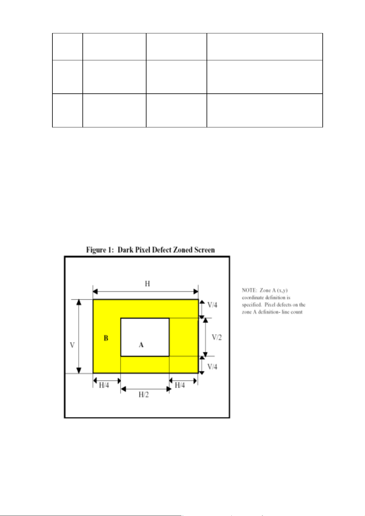
1.7 Mirror Defects / Dot Defects Dark pixels<=2, bright pixels =0 (See Appendix D)
1.8 Image Distortion Pincushion 1.0%
3
Page 5
Keystone 1.0%
1.9 Descriptive Image Quality There should be no streaks or jitter, good saturated colors, and
crisp resolution. Must adhere to Appendix E
1.10 Lateral Color 1 Pixel
1). 52” Diagonal for OPT test;
1.11 Screen Size for Testing
2). Distance 3.0m for Focus test. ( Tele @ the same Throw
Distance. )
Criteria: Pixel clear ( same as test chart )
2.0 Optical
2.1 Optical Structure Single Chip 0.8” 12° tilt DMD ( HD2 ) from Texas Instruments
(HD2 Front Projection Image Quality Specification described in
Appendix D)
2.2 Projection Lens Manual Zoom & Focus
2.2.2 F/#
2.8
2.2.3 Throw Ratio 100” Diagonal at 3m ( Wide )
2.2.4 Zoom Ratio 1.2 : 1
2.2.5 Focus and flare As following chart:
2.3 Lamp
2.3.1 Maker Ushio
2.3.2 Model NSH 210 MD
2.3.3 Type DC lamp
2.3.4 Lamp Wattage 210 watts
2.3.5 Lamp life 1000 Hours ( Typical )
2.4 Focus Distance 1.5 – 5m
2.5 Keystone Correction
2.5.1 Electronic ± 12°
2.6 Colors 24-bit color
2.7 Native Resolution
4
Page 6

2.7.1 PC Mode 1280 x 720 pixels
1280 x 720 pixels
2.7.2 Video Mode
3.0 Mechanical & Cosmetic
3.1 Dimensions 400L x 347W x 116H
3.2 Weight 16.7 lbs (7581 g)
3.3 Security Slot Kensington compatible slot 150N break away force
3.4 Feet 4 adjustable feet
3.5 Lamp Replace Position Front
4.0 Compatibility Supporting timing: see appendix E
4.1 RGB PC Compatible VGA, SVGA, XGA
4.2 Video Signal Composite, S-Video, Y/CB/CR
4.3 HDTV DTV Y/PB/PR , DTV RGBHV ,DTV DVI-I ( 480P, 1080i, 720P,
576P, 540P)
4.4 Image Inversion Mirror, Upside-down, Mirror Upside-down
4.5 Scaling Scaling from other resolutions to native by O-plus
chip
TM
scaling
4.6 Aspect ratio ANAMORPHIC, 4x3, LETTER BOX, VIRTUAL WIDE.
5.0 Interface Connectors
5.1 RGB Input DVI x 1 (include 5.2.5)
5.2 Video Input
5.2.1 Composite
RCA x 1
5.2.2 S-Video S-Video x 1
5.2.3 Component RCA x 3
5.2.4 Progressive component
BNC x 5
and DTV RGBHV
5.2.5 Digital Video DVI x 1 with HDCP
5.3 RS232C Input
Telephone jack
6.0 Electrical
6.1 RGB
6.1.1 Input
6.1.1.1 Amplitude 0.7 ± 0.1 VPP at 75Ω termination, positive bright
6.1.1.2 Input
75Ω
Impedance
6.1.1.3 Synch TTL compatible
6.1.2 Computer
Compatibility
The unit should be compatible with normal computer formats
ranging from VGA to XGA.
6.1.3 Video Compatibility Don’t use BUBUKAU DVD for test equipment.
5
Page 7

6.2 Control
6.2.1 IR Receivers
6.2.1.1 Location 2receiver, located on the front and rear of this projector
6.2.1.2 Range 8m ( front ) / 5m ( rear ) with 30 degree horizontal Angle and 15
degree vertical angle
7.0 Power Requirements
7.1 Power Supply VAC 100 – 240 Full range switch (50/60Hz), 3 Wire Grounded
7.2 Power Consumption 310W max.
7.3 Power Connector
8.0 Audible Noise Level
IEC
34 dB (
Max) @ 25℃ sea level
9.0 Thermal
9.1 Surface Metal
9.2 Surface Plastic
9.3 Exhaust Air
9.4 Screws, Terminals
60°C
65°C
80°C
70°C
10.0 Contamination
10.1 Prevention Optical system is closed
10.2 Dust in Optical Path No noticeable dust
11.0 Included Accessories
11.1 Cables Power Cord Set (US, UK, Euro) x 1, VGA Cable (1.8m) x 1,
Projector Common Cable x 1
11.2 Printed Matter User’s manual
11.3 Remote Control IR Remote x 1, AAA Batteries x 2
12.0 User Interface
12.0 Backlight
12.1 Operator Panel YES
12.2 Indicators Power Status LED, Lamp Status LED
12.3 Remote Control Front IR receiver , Rear IR receiver
12.4 Onscreen Menu Should be in 3 languages (English, French, Spanish )
12.8 User’s Manual Should be in 3 languages (English, French, Spanish )
13.0 Reliability
13.1 General Failure Def. See Appendix B
13.2 MTBF 20000 hours except for DMD chip , lamp , fans and color wheel.
14.0 Environmental
14.1 Operating 10 – 35°C, 20 – 90%RH, without condensation
14.2 Storage -10 – 70°C, 20 – 90%RH, without condensation
14.3 Altitude
14.4 Shock
NO
0 – 6000 feet above sea level, ambient 30 ℃
6
Page 8
14.4.1 Straight Drop 50mm
14.4.2 Tilt Over Should be able to fall over from tilting without taking any
damage. Must Adhere to Appendix B
14.5 Gas No corrosive, toxic, or combustible gas should be emitted
14.6 Electrostatic Discharge comply to the acceptance criteria as specified in EN
61000-4-2/1995
15.0 Regulatory UL, CE, FCC Class B. Must Adhere to Appendix B Section 10.0
15.1 Safety Requirements UL compliance: UL6500 (2th Version)
CSA compliance: E60065-00
TUV compliance: IEC60065:2001
CCC: GB8898; GB13837; GB17625.1: 1998
15.1 EMI Requirements 1. CE Mark compliance: EMC: 89/336/EEC
EN 55013:1990+A12 :1994+A13 :1996+A14 :1999
EN 61000-3-2:1995+A1 :1998+A2 :1998+A14 :2000
EN 61000-3-3:1995+A1 :2001
EN 55020:1994+A1 :1996+A12/A13/A14 :1999
IEC 61000-4-2/2001
16.0 Packaging
16.1 Packaging Form Must adhere to attached file
16.1.1 Dimensions 537 x 520 x 260 mm
16.1.2 Weight TBD
16.1.3 Palletization 1140 x 1050 x 120 mm
16.1.4 Carton Labeling Must adhere to attached file
16.2 Vibration Must adhere to Appendix B
16.3 Drop Test Must adhere to Appendix B
IEC 61000-4-3/2001
IEC 61000-4-4/1995+A1:2000+A2:2001
2. FCC
FCC Part 15B
3. C-Tick
ASIN2S 1053:1996
4. VCCI
VCCI/2002(15
th
Edition)
7
Page 9

Appendix A Optical Measurement
This part of the Optical Test Instruction describes those measurements to be executed
during the production of the optical engines.
Content:
A1 BRIGHTNESS
A2 BRIGHTNESS UNIFORMITY
A3 BRIGHTNESS DIFFERENCE
A4 ANSI CONTRAST
A5 PEAK CONTRAST
A6 LIGHT LEAKAGE
A7 IMAGE DISTORTION
A8 THROW RATIO
A9 ZOOM RATIO
A10 FOCUS RANGE
A11 COLOR
A12 COLOR UNIFORMITY
A13 OPTICAL KEYSTONE (FIXED)
General requirements
1. The unit shall be allowed to stabilize without further adjustment for a
minimum of 10 minutes, at nominal ambient room temperature of 25°C,
before making measurements.
2. Measurements shall take place in a light proof room, where the only source of
illumination is the projector. Less than 1% of the light on the screen shall be
from any source other than the projector.
3. All measurements shall be made on flat screens that do not provide any
advantage to the performance of the unit
4. All measurements shall be made at standard color temperature setting, 100%
white image (per ANSI IT7.228-1997), except where noted
8
Page 10
Practical consideration
+++++++
1. When measuring contrast manually, operators should not wear white
clothing since light reflected from white clothing can influence the
measurement.
2. Unless otherwise specified the projection lens is set in the widest zoom
position since zoom function can influence the measurement.
3. Measurement should be performed with Minolta Chromameter, Model
CL-100, or equivalent.
A1. BRIGHTNESS
Unit: Lumen
Brightness: Default
Contrast: Default
W: width of projected image; H: height of projected image
A (Area) = W * H (in meters)
987654321
ANSI Lumens = )()(
+
LLLLLLLLL
2
mAlux
∗
9
1
W
3
1
W
6
1
H
6
1
H
3
9
Page 11
A2. BRIGHTNESS UNIFORMITY
Unit: %
Brightness: Default
Contrast: Default
Uniformity =
EEEEMIN
1/20w
)13,12,11,10(
987654321
LLLLLLLLL
++++++++
9
E10
L5
E12
E11
E13
A3. BRIGHTNESS DIFFERENCE
Unit: %
Brightness: Default
Contrast: Default
Brightness Difference=
−
1/20h
))13,12,11,10()13,12,11,10((
EEEEMINEEEEMAX
9
987654321
LLLLLLLLL
++++++++
A4. ANSI CONTRAST
Unit: Contrast : 1
Brightness: Default
Contrast: Default
Contrast Ratio shall be determined from illuminance values obtained from a
black-and-white ”chessboard” pattern consisting of 16 equal rectangles. The
white rectangles shall be at 100% gray and the black rectangles at 0% gray.
Illuminance measurements shall be made at the center of each of the rectangles.
Contrast Ratio = Average lux value of the white rectangles/Average lux value
of the black rectangles
10
Page 12
−
+
A5. PEAK CONTRAST
Unit: Contrast : 1
Brightness: Default
Contrast: Default
Contrast Ratio = Lux value at the center of a solid white screen/the lux value
of a solid black screen
A6. LIGHT LEAKAGE
Unit: Lux
Brightness: Default
Contrast: Default
Leakage = The maximum light leakage of a solid black screen outside the
projected image
A7. IMAGE DISTORTION
Unit: %
Brightness: Default
Contrast: Default
Measurement procedure:
Measure the dimensions H1, H2 and H3, with H3 at the half image width, as
shown above for both zoom settings. For each the distortion is defined as:
3*221
distTV
=−
H
HHH
%100*
3*2
All should be within the absolute specification tolerance.
A8. THROW RATIO
Unit: Ratio : 1
Brightness: Default
Contrast: Default
Throw ratio = projection distance / the width of the projected image
11
Page 13
−
A9. ZOOM RATIO
Unit: Ratio : 1
Brightness: Default
Contrast: Default
Zoom ratio = maximum / minimum image diagonal size at a fixed projection
distance.
A10. FOCUS RANGE
Unit: m (Max~Min)
Brightness: Default
Contrast: Default
The minimum/maximum focus distance is the minimum/maximum projection
distance (front side projection lens and the image lane), expressed in meter,
at which the image is still at its best for focus.
A11. COLOR
Unit: x, y
Measurements at the center (except in the case of color uniformity
measurements) of a screen which is entirely of the color being measured and
at default brightness and contrast
settings.
A12. COLOR UNIFORMITY
Unit: x, y
Difference between any two points out of Lx and Ex should not exceed the
specification for the given color.
A13. OPTICAL KEYSTONE (FIXED)
Unit: %
Brightness: Default
Contrast: Default
Measure the dimensions W1, W2 and W3 at the half image height, as shown
above. The distortion is defined as:
WW
distTV
−
=− & %100*
%100*
distTV
=−
331W
WW
332W
12
Page 14

Appendix B Design Verification Test Procedure
1.Purpose
This standard establishes the environmental specification for projector related
products, which defines the level of product performance and reliability in the field. It is not
necessary the intent of these specification to simulate a typical user environment, but rather
to provide for a level of product robustness that when applied over a wide range of
manufacturing variability and environmental usage conditions.
2.Test Summary
Dynamic Testing Specification
Package Drop 76cm, 1 drop per orientation, all 6 primary surfaces, plus a selected
corners, and three selected edges, total of 10 drops
Package Vibration
Shock, non-operating 50g, 20ms half-sine, all primary axis, 1 shock per orientation, total of 3
Security Lock 150N break away force
Fragility
Atmospherics
Temperature/Humidity,
operating
Random , 0.01g2/Hz, 5~100Hz, all primary axis, 20 min per orientation,
total of 60min
Sine, 0.5g, 5~200Hz, 1 octave/min, 15 min dwell on each resonant
frequency, all primary axis, one sweep (30min minimum) per orientation,
total of 90+min
shocks
Shock, 50g, 20ms half-sine, all primary axis, 1 shock per orientation, total
of 3 shocks
Accelerate Life Test (operating), 65
Thermal shock(bare board), -65~125
Input Voltage, 90~264V
Input RGB signal, 0.7V±0.1
10~35oC/10~80RH, 48hr
o
C, 72hr
o
C, 48hr
Temperature/Humidity,
non-operating
Altitude, operation
Safety/EMC
UL/cUL
TUV Rheinland
Fcc/CE/C-Tick
-10~70oC/10~80RH, 48hr
0~6000ft@30oC, 4hr
13
Page 15

3.Definition
3.1 Failure Criteria:
The product is expected to perform to its full potential without loss of function,
performance, critical parametric changes, and other undesirable anomalies, over the
applied boundaries of this specification. The following product failure are not allowed within
the boundaries defined in this specification:
1.Failure including permanent damage, critical parametic changes (optical
performance defined in Appendix A), and latent defects.
2.Failure requiring operator intervention.
3.Failure violating external laws, regulatory agency standards, and government
directives.
4.Failure resulting in a safety, potential safety, issue.
3.2 EUT: Equipment under Test
3.3 Q: Peak Acceleration Response divided by acceleration input peak
4.Test Order
Atmospherics, Dynamic, and Safety test sets require separate units and can be
processed in parallel. EUT testing shall be performed serially within each set.
Set 1 (3 units) Set 2 (3 units) Set 3
Dynamics: Atmospherics: Safety/EMC:
Package Drop Temperature/Humidity, Operating EFT
Package Vibration Temperature/Humidity,
ESD
Non-operating
Shock Altitude, Operating EMI-Radiated
Bench Drop Aging EMI-Conducted
EMI-Susceptibility
14
Page 16
Appendix C Drawings and Attachments
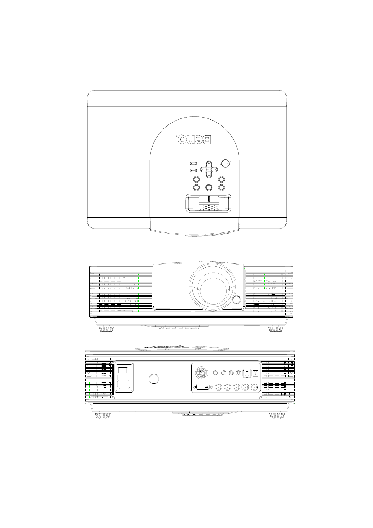
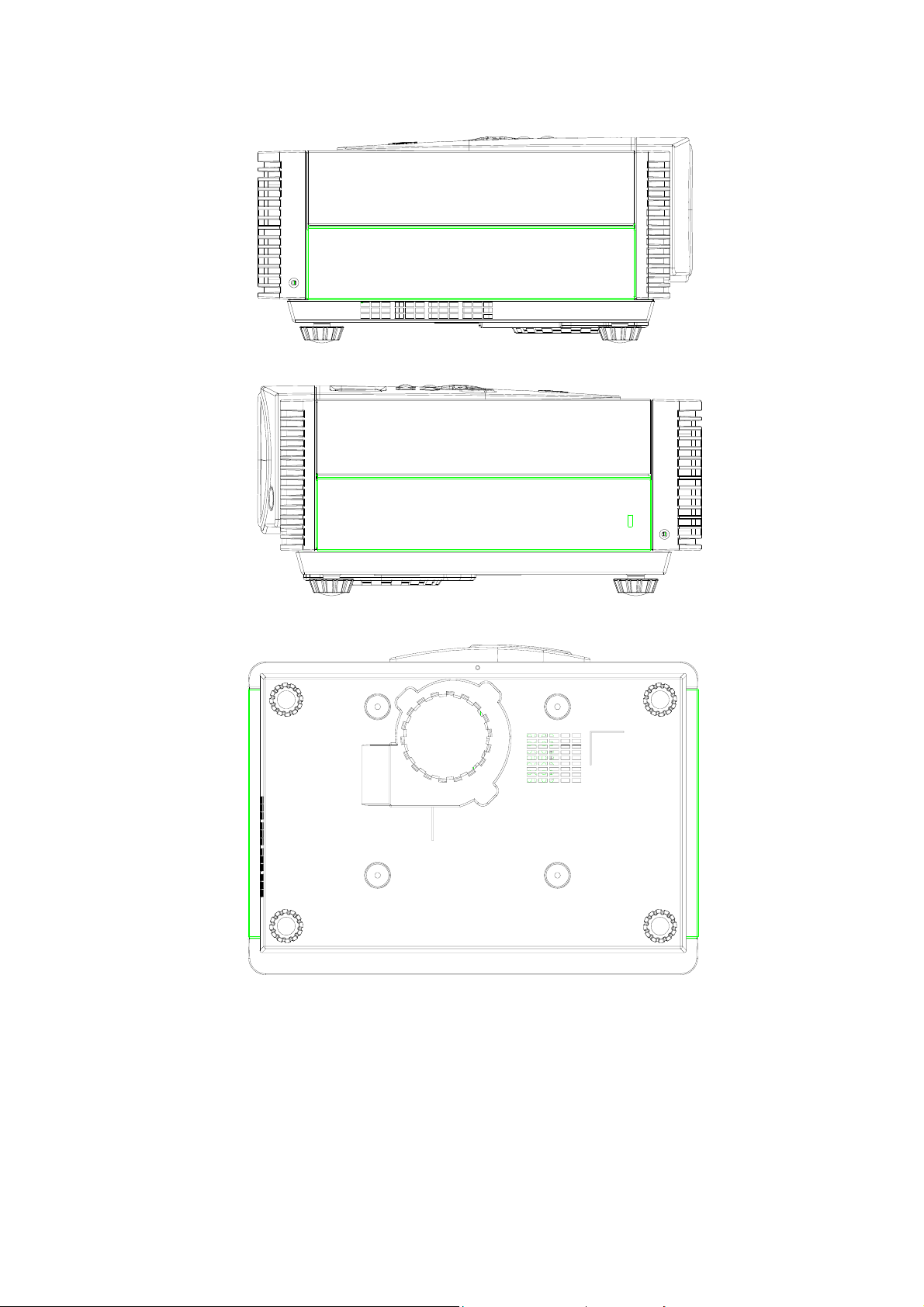
Drawing 1: Top view of BENQ PE8700 video projector
15
Page 17
16
Page 18

Appendix D HD2 Front Projection Image Quality Specification
1. SCOPE
This document specifies the image quality requirements applicable to the HD2 Component
Set for Front Projection image display. The HD2 Component Set provides digital imaging
functionality based on Digital Micromirror Device (DMD) technology.
2. DEFINITIONS
2.1 Blemish
A blemish is an obstruction (dark blemish), reflection, or refraction of light (light blemish)
that is visible, but out of focus in the projected image under specified conditions of
inspection (see Table 1). It is caused by a particle, scratch, or other artifact located in the
image illumination path.
2.2 Dark pixel
A dark pixel is a single pixel or mirror that is non-functional (stuck) in the OFF position.
2.3 Bright pixel
A bright pixel is a single pixel or mirror that is non-functional (stuck) in the ON position.
2.4 Unstable pixel
An unstable pixel is a single pixel or mirror that does not operate in sequence with
parameters loaded into memory. The unstable pixel appears to be flickering
asynchronously with the image.
2.5 Adjacent pixels
Adjacent pixels are defined as sharing a common border or common point.
2.6 Border defects
Border defects are bright blemishes (see 2.1) or bright pixel defects (see 2.3) in the
non-active area that may be visible in front projection mode.
2.7 Blue test screen
This screen is used to test for major dark blemishes and dark pixels. All areas of the screen
are colored at a specific blue level, based on MS Paint 0-255 RGB scale:
Major Dark Blemish
Blue Value 90
Red Value 0
Green Value 0
17
Page 19
2.8 Gray 6 test screen
This screen is used to test light blemishes and bright pixels. All areas of the screen are
colored at a specific gray level, based on MS Paint 0-255 RGB scale:
Major Light Blemish
Blue Value 6
Red Value 6
Green Value 6
2.9 Gray 10 test screen
This screen is used to test light blemishes and bright pixels. All areas of the screen are
colored at a specific gray level, based on MS Paint 0-255 RGB scale:
Major Light Blemish
Blue Value 10
Red Value 10
Green Value 10
2.10 White test screen
This screen is used to test light border blemishes and bright pixels. All areas of the active
area are colored at a specific gray level, based on MS Paint 0-255 RGB scale:
Major Dark Blemish
Blue Value 255
Red Value 255
Green Value 255
2.11 black test screen
This screen is used to test light border blemishes and bright pixels. All areas of the active
area are colored at a specific gray level, based on MS Paint 0-255 RGB scale:
Major Dark Blemish
Blue Value 0
Red Value 0
Green Value 0
18
Page 20
2.12 Red Ramp test screen
This screen is used to test light border blemishes and bright pixels. All areas of the active
area are colored at a specific gray level, based on MS Paint 0-255 RGB scale:
Major Dark Blemish
Blue Value 0
Red Value Start 0,end 255
Green Value 0
3. ACCEPTANCE REQUIREMENTS
3.1 Test Conditions (as tested in OEM projector)
· Projector degamma correction shall be linear. Using HD Control “Curtain” Mode is
equivalent.
· Image noise reduction algorithms “Blue Noise STM” and “Boundary Dispersion” shall be
set to “off”.
· Projector shall be used in front projection mode using a customer-specified screen, and
OEM optical system.
· The diagonal size of the projected image shall be 52 inches (132cm).
· The projected image shall be inspected from a 60 inches (1.52 meter) minimum viewing
distance.
· Projector will be properly focused on the DMD array as shown on the screen.
· Testing time is limited to 20seconds per screen.
· Refer to Table 1 for acceptance criteria, in specified order:
TEST
ORDER
1 Major Dark Blemish Blue 90 No dark blemishes visible on Blue 90
2 Dark Pixel Blue 90
3 Border Defects Gray 10 No border defects visible
4 Major Light Blemish Gray 6 No light blemishes visible on Gray 6
TEST SCREEN ACCEPTANCE CRITERIA
0 dark pixels allowed in Zone A
Zoned Screen (see
below figure 1)
<=2 dark pixels allowed in Zone B
No adjacent dark pixels
19
Page 21
5 Light Pixel Gray 6 No light pixels visible on Gray 6
6 Minor Blemishes White or Black
7 Unstable Pixel Red Ramp
Screen(or any
other
TABLE 1. Image Quality Specification
Total of Dark and Light Blemishes ≦
4
(See Test 4 , 5)
No unstable pixels
Notes:
1. The acceptance basis for all cosmetic DMD defects will be the projected image tests
referenced in Table 1.
2. Projected blemish numbers include the shadow of the artifact in addititon to the artifact
itself.(Count=4)
4. The projected image shall not contain any blemish more than 15 cm long, measured on
a 1.32m diagonal screen.
20
Page 22
Appendix E Supporting Timings
Table 1: Support Timings by DVI-I Input (Analog or Digital PC signals)
Resolution Vert. Freq
(Hz)
1 VGA 640 x 400 70.089 31.470 25.167 D/A -/+
2 VGA 640 x 480 59.590 31.470 25.167 D/A -/-
3 VGA 640 x 480 85.008 43.269 36.0 D/A -/-
4 SVGA 800 x 600 60.317 37.879 40.0 D/A +/+
5 SVGA 800 x 600 75.000 46.875 49.5 D/A +/+
6 SVGA 800 x 600 85.061 53.674 56.25 D/A +/+
7 XGA 1024 x 768 60.004 48.363 65.0 D/A -/-
8 XGA 1024 x 768 75.029 60.023 78.75 D/A +/+
9 XGA 1024 x 768 84.997 68.677 94.5 D/A +/+
Table 2: Support Timing by DVI-I Input
Index Format
name
Line
Rate
Pixel
Rate
Frame
Rate
Line
active
Hori. Freq
(kHz)
Line
total
Frame
active
Pixel freq
(MHz)
Frame
total
Digital (D)/
Analog (A)
H back
porch
H sync
width
Polarity
V back
porch
V sync
width
(kHz)
1 480p59 31.469 27 59.94 720 858 480 525 59 63 30 6
2 576p50 31.25 27 50 720 864 576 625 68 64 39 5
3 720p50 37.5 74.25 50 1280 1980 720 750 260 40 20 5
4 720p59 44.955 74.176 59.94 1280 1650 720 750 260 40 20 5
5 720p60 45 74.25 60 1280 1650 720 750 260 40 20 5
6 1080i25 28.125 74.25 25 1920 2640 1080 1125 148 44 15 5
7 1080i29 33.716 74.176 29.97 1920 2200 1080 1125 192 44 15 5
8 1080i30 33.75 74.25 30 1920 2200 1080 1125 192 44 15 5
(MHz)
(HZ)
(pixel)
(pixel)
(line)
(line)
(pixel)
(pixel)
(line)
(line)
21
Page 23
Table 3: EDTV and HDTV Timing supported by component (YPBPR) and RGBHV Input
Index Format
name
1 480i 15.734 13.5 59.94 720 858 480 525 59 63 30 6
2 576i 15.625 13.5 50 720 864 576 625 68 64 39 5
3 480p 31.469 27 59.94 720 858 480 525 59 63 30 6
4 576p 31.25 27 50 720 864 576 625 68 64 39 5
5 720p50 37.5 74.25 50 1280 1980 720 750 260 40 20 5
6 720p59 44.955 74.176 59.94 1280 1650 720 750 260 40 20 5
7 720p60 45 74.25 60 1280 1650 720 750 260 40 20 5
8 1080i25 28.125 74.25 25 1920 2640 1080 1125 148 44 15 5
9 1080i29 33.716 74.176 29.97 1920 2200 1080 1125 192 44 15 5
10 1080i30 33.75 74.25 30 1920 2200 1080 1125 192 44 15 5
Line
Rate
(kHz)
Pixel
Rate
(MHz)
Frame
Rate
(HZ)
Line
active
(pixel)
Line
total
(pixel)
Frame
active
(line)
Frame
total
(line)
H back
porch
(pixel)
H sync
width
(pixel)
V back
porch
(line)
V sync
width
(line)
22
Page 24

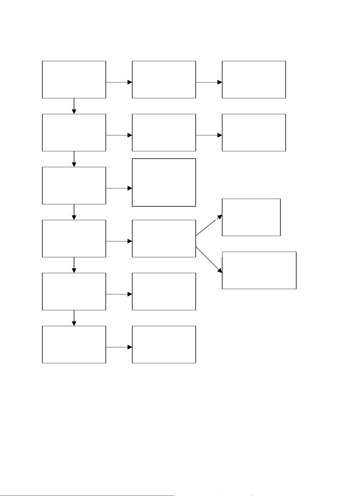
Chapter 4 Spare Parts List
Projector PE8700 99.J5877.B21
NO Parts NO Description
1 55.J2003.001 IR BD HT480W MI
2 55.J5801.011 PCBA MAIN/BD FOR BENQ
3 55.J5824.001 PCBA DMD BOTTOM/BD HT720G
4 55.J1313.001 PCB 1L SENSOR-B BD SL700 X MI
5 65.J2004.001 COLOR WHEEL SIX SEGMENT UNAXI
6 55.J5802.001 PCBA DMD/BD HT720G
7 65.J5801.001 ASSY LENS ZOOM HT720G PROT
8 71.00HD2.A00 IC MUSTANG DMD PREMIUM CLGA
9 65.J3403.001 ASSY BALLAST210W/USHIO DX660
10 55.J2006.010 PCBA KEYPAD/BD HT720G BENQ
11 55.J5817.001 PCBA TRANSLATION/BD HT720G
12 60.J2020.021 ASSY CVR BASE HT720W/BENQ
13 60.J2023.022 ASSY L/C HT720W/BENQ
14 60.J2037.011 ASSY CVR FRONT HT720W/BENQ
15 60.J2038.011 ASSY CVR BACK CONTOR HT720W
16 60.J2112.001 ASSY CVR LENS HT720W BENQ
17 55.J2013.001 PCBA THERMAL SENSOR/B HT480W
18 55.J2021.001 PCB FPC/BD FOR HT480W
19 55.J5810.011 PCBA CONNECTOR/BD FOR BENQ
20 55.J2005.001 PCBA POWER BD HT480W MI
21 55.J5811.001 PCBA PFC/BD HT720G
22 44.J2003.021 CTN AB 455X500X228 HT720G/BEN
23 47.J2008.001 CUSHION FRONT EPE HT480W
24 47.J5804.001 CUSHION REAR EPE HT720G BENQ
25 50.J2103.501 CABLE RGA/DVI-A (WHDDC) 1.8M
26 50.L2508.501 SIGNAL/C DUAL DVI-D/DVI-D 200
27 60.J2028.R01 ASSY AV CABLE RUNCO CL-500
28 98.J2032.B01 HT480W BENQ REMOTE CONTROL
29 60.J2104.CG1 ASSY CSD LAMP MODULE PE8700
23
Page 25
5. Black Diagram
RGB DVI
RGB PC
RGB/YPbPr
BNC
YCbCr
YPbPr
S-video
Video
YCbC r
RS232 RJ11
IR (TOP)
12V Trigger O/P
IR (fron t) IR Board
Conntctor Board Main Board
Sil169
(U17)
MUX
(U2,U3,U4)
IR Board
MUX
(U5)
RS232
Download
(U14)
IR
(U12)
12V
(Q2,Q3)
IR
Board
ADC AD9883
(U7)
Video Decoder
SAA7118
(U10)
SDRAM
(U3)
Keyboard
De-inter lace
SII504
(U2)
MCU503
(U4)
Video Port
Scaler
RM1-A
(U5)
CPU RDC8820
(U10)
Fan
Driver
(U1,U3)
Translatio n Board
Protec tion
Circuit
(U4)
Reset IC
(U18)
SDRAM
(U19,U20,
U21)
SRAM
(U9)
Frash
(U12)
RS232
Hardware
Monito r
(U14)
DMD Board
HD2
DMD
Color
Cheel
Blaster Lamp
400V
PFC
Board
Power
Board
3.3V
5V
12V
Therm al
Sensor
Fans
Therm al
Break
24
Page 26
6. Packaging Description
25
Page 27
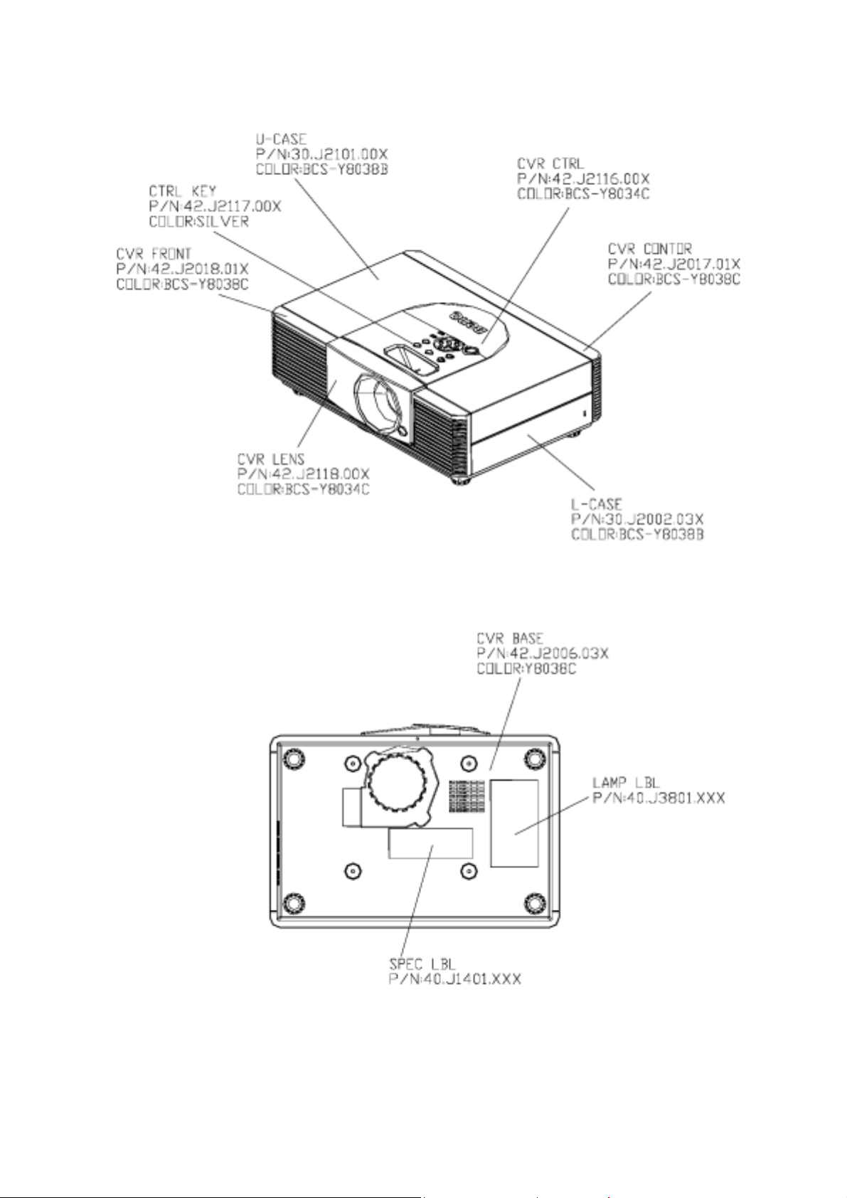
7. Appearance Description
26
Page 28
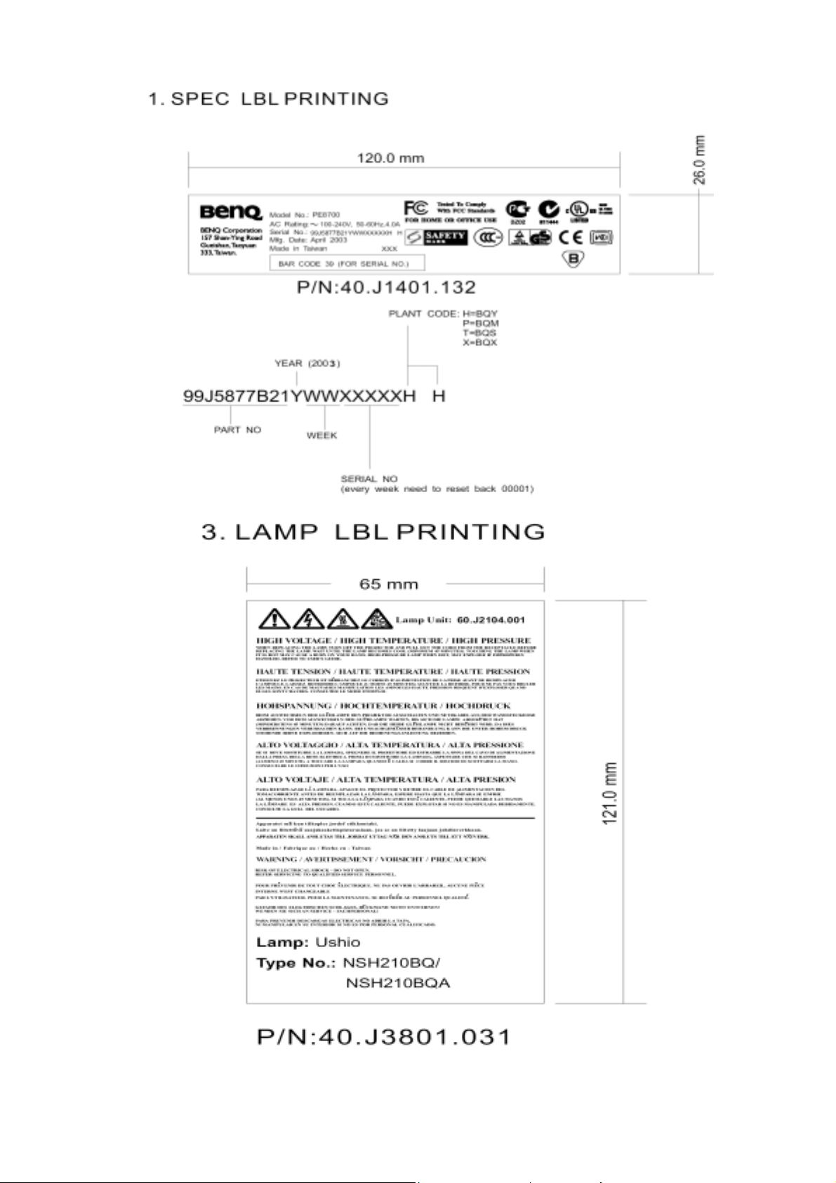
27
Page 29
8. Alignment Procedure
1. DMD Bias Voltage Alignment
Equipment:
- None
Procedure:
1. Watch DMD chip Label
2. Switch the DIP switch on DMD board according to the character on the DMD chip
B C D E
1 of SW H1 1 0 1 0
2 of SW H2 1 1 0 0
0: Left; 1:Right
2.Color Wheel Delay Alignment
Equipment:
- Battery Biased Silicon PIN Detector
- Oscilloscope
- Probe
OSD Default value used for color delay alignment
Item Value Item Value
USER>DVI-A> Factory>DLP>
Brightness 0 Brightness 0
Contrast 30 Contrast 49
Color 60 CW delay 20
Tint 15 User>Setup>Whit
Sharpness 0 Red Gamma 66
Filter 2 Green Gamma 66
Color Temp 0 Blue Gamma 66
R gain 512
G gain 512
B gain 512
R Offset 0
G Offset 0
B Offset 0
The default values let optical engine to get maximum contrast and brightness.
28
Page 30
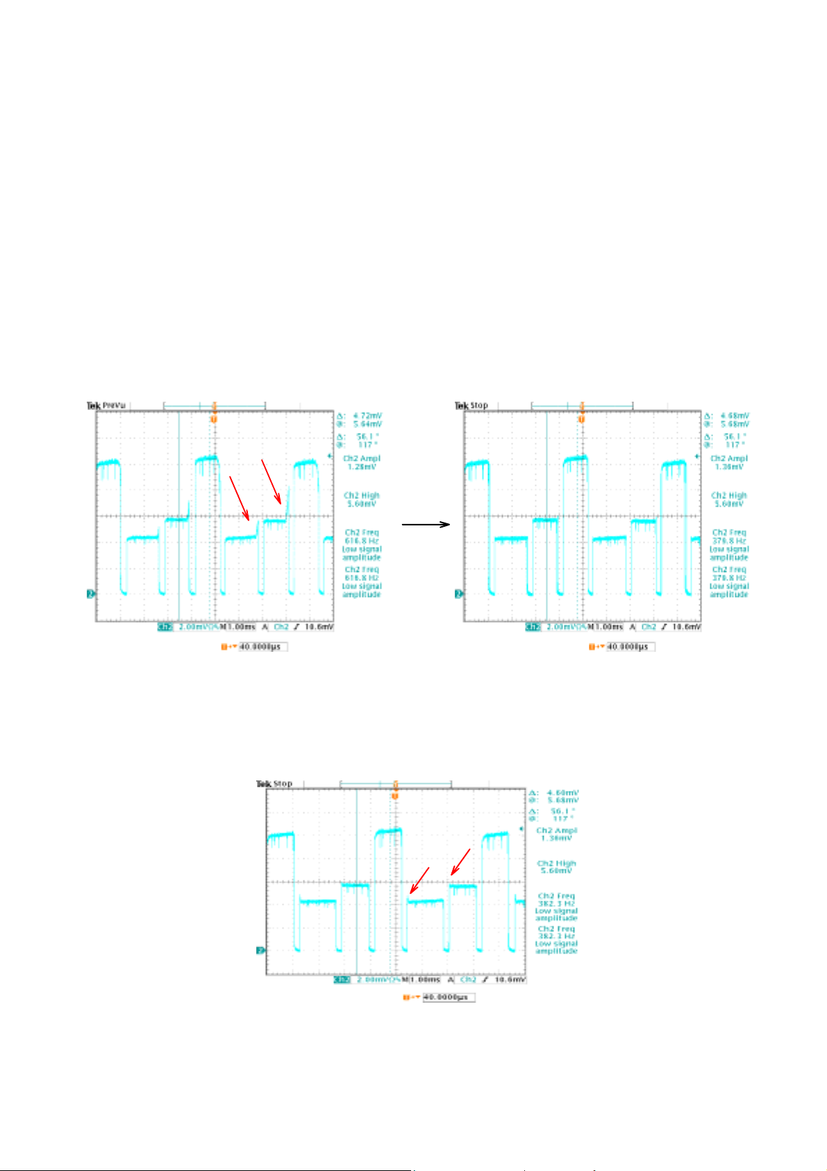
Procedure:
1. Probe impedance matches 50 ohm
2. Change Timing and pattern of pattern generator :
Timing : 800x600@60Hz (H:37.879Khz,V:60.317Hz)
pattern : full white
3. Adjust user & factory OSD values to default.
4. Open Factory OSD, and select color wheel delay item.
5. The image will become white.
6. Put the detector on the screen that white image was projected.
7. Watch the oscilloscope and notice the square waveform
8. Use the “” and “” key to increment or decrement the color wheel delay value
9. No matter the waveform is square or not, let the waveform was lagged first
Lag Exact
10. Then increment or decrement the value to let the waveform to be square
11. Do not adjust too much, let the signal get ahead, if it happens, go back to step 7 and do
it again.
Ahead
12. Select “Save Setting” at “Factory OSD>Factory>”.
29
Page 31

3. DVI-Analog Color Alignment Procedure
Default valve(User menu)
contrast color Sharpness
Video 17 23 3
S-Video 17 23 1
Comp 17 30 0
Comp-HD 17 30 3
RGBHV 17 30 3
DVI-I 17 30 1
The Gamma(RED ,GREEN,BLUE) is 66 for temperature 0,1,2,3,4.
Equipment:
- Pattern generator (Chroma 2250)
- Lux meter ( CL-100)
OSD Default value used for DVI-Analog color alignment
Item Value Item Value
USER>Picture> Factory>HDADJ>RG
Brightness 30 R offset 55
Contrast 17 G offset 63
Color 30 B offset 62
Tint 15 R Gain 89
Sharpness 1 G Gain 89
Filter 1 B Gain 89
Color Temp 2
Factory>DLP
Brightness 0
Contrast 49
User>Setup>White
Gamma Red, Green, 66
Gamma Red, Green, 0
30
Page 32

+
Procedure:
A. Black Level Adjustment: (DLP brightness)
1. Change pattern of pattern generator :
Pattern : Black (Gray 0)
2. Adjust DLP Brightness to let the black picture to just distinguish.
B. White Level Adjustment: (AD contrast---R,G,B gain)
1. Change pattern of pattern generator :
pattern : White (100% Gray)
2. Use Lux meter to measure the white level. Adjust the contrast value of AD9883 (RGB)
to let the light output to just max.
3. Change to 32-gray (0 ~ 100%) pattern. All steps must appear,
C. Offset adjustment at low brightness (AD R, G, B offset)
1. Change Timing and pattern of pattern generator :
pattern : 10% Gray
2. Set user color temp to 6500K.
3. Adjust AD9883 Red and Blue Offset to meet 6500K color spec.
D. Color Temperature at high brightness (Scalar Gamma R, G, B Gain)
1. Change Timing and pattern of pattern generator :
Timing : 800x600@60Hz (H:37.879Khz,V:60.317Hz)
Pattern : 80% gray
2 Color temperature spec: CIE 1976 u’, v’ chromaticity)
Color temperature
'
27
=
x
=
y
'
=
u
'
=
v
u
''
−
12
4
9
364818
vu
'
v
''
364818
+−
vu
x
3122
++−
yx
y
3122
++−
yx
5400°K 6500°K 7500°K
0.333 0.312 0.296
0.333 0.329 0.316
0.210 0.197 0.190
0.473 0.468 0.459
Deviation:
u’v’=
( vu ∆+∆
2
'
2
'
<=0.010 <=0.010 <=0.010
Color Temp 4 = color temp is the same as that of 6500K
31
Page 33
3 The variance of color coordinate via R,G,B gains:
x Y
R ↓ X ↓
G ↓
-
-
y ↓
B ↓ X ↑ y ↑
4. Adjust 6500K temperature color by changing Gamma-Rgain, Ggain, and Bgain.
5. Open Factory OSD and set the factory default value :
user>setup>white C0 C1(5400k C2(6500k C3(7500k
Gamma-Rgain 512 512 512 512
Gamma-Ggain 512 412 467 479
Gamma-Bgain 512 398 452 490
User the lux meter and adjust Gamma-Rgain, Gamma-Ggain, & Gamma-Bgain to
meet the spec.
6. Press “Save Graphics Color Temp” to save current setting into memory.
7. Select “Save Setting” at “Factory OSD>Factory>”.
8.Change pattern to 10% gray pattern and measure the color temp. If 6500K color spec is
not met, repeat all procedures in C and D.
9. Follow step 1 to 8 to adjust 5400K, 7500K color temperature.
10. For auto-alignment, use Command Y31/Y32/Y33 to save 5400K/6500K/7500K
temperature
11. For auto alignment, use Command to reset Temp4 color temp to 6500K
4. YPBPR Color Alignment
(A) YPbPr Component:
Equipment:
- Pattern generator (VG-828)
- Lux meter ( CL-100)
OSD Default value used for YPBPR color alignment
Item Value Item Value
USER>Picture>
Brightness 30
Contrast 17
Color 30
Tint 15
Sharpness 3 Brightness 60
Factory>HD ADJ>YPbPr>
32
Page 34

Filter 1 Contrast 76
Color Temp 2 Saturation 49
Pb offset 60
Pr offset 60
Procedure:
(a). PBPR Offset adjustment: (AD PB, PR Offset)
1. The variance of color coordinate via Pb offset and Pr offset:
x y
Pb offset ↓ x ↓ y ↓
Pb offset ↑ x ↑ y ↑
Pr offset ↓ x ↑ y ↓
Pr offset ↑ x ↓ y ↑
If we line the x and y, then the Pb offset is the shift action and the Pr offset is the
rotational action.
2. Connect power, YPbPr Video into projector.
3. Change Timing and pattern of pattern generator :
Timing : 480P(H:31.54 KHz,V:60.08 Hz)
pattern : 10gray Pattern
4. Turn on projector
5. Set user OSD values to default.
6. Enter factory mode.
7. Set Factory values to default.
8. Follow the Pb, Pr offset adjustment flow chart to adjust color temperature to 6500K
b). Gray Level: (AD YPBPR Contrast, Brightness)
1. Change Timing and pattern of pattern generator :
Timing : 480P(H:31.54 KHz,V:60.08 Hz)
pattern : gray 32( or gray16 only for overscan)
2. Adjust the Brightness of AD9883 (RGB) to let the black level of the gray
32 to just distinguish. Use Lux meter to measure the white level of the gray 32. Adjust
the contrast value of AD9883 (RGB) to let the light output to just max.
3. Check the 32 levels of gray. All steps must appear,
33
Page 35

(c). Saturation Level: (Scalar)
1. Change Timing and pattern of pattern generator :
Timing : 480P(H:31.54 KHz,V:60.08 Hz)
pattern : 100% blue
2. Adjust saturation and use lux meter to measure to let the light output just max.
3. Select “Save Setting” at “Factory OSD>Factory>”.
Use L ux m ete r to
read the coordinate of
black and the value
note (x1,y1).
Case
x1>x0 & y1>y0
Decrease Pb offset
until x<=x0 or
A B C
Case x<=x0:
The value note (x2,y2).
Dy = y2 - y0.
Decrease Pb o ffset until the y
value <= y2 - 1/2Dy . Now, the
reading of the Lux meter =
(x3,y3) and x3 will < x0, y3 will
> y0.
Decrease Pr offset the x value
will increa se an d y v alue w ill
decrease to meet the sp ec.
y<=y0
Case y<=y0:
The value note (x2,y2).
Dx = x2 - x0.
Decrease Pb offset until the x
value <= x2 - 1/2Dx . Now, the
reading of the Lux m eter =
(x3,y3) an d x 3 w ill > x0 , y3 w ill
Increase P r offset th e x va lue w ill
decrease and y value will increase
to meet the spec.
< y0.
Increase Pb offset
Case x>=x0:
The value no te (x2,y2).
Dy = y0 - y2.
Increase Pb offset until the y
value >= y2 + 1/2Dy . Now, the
reading of the Lux meter =
(x3,y3) and x3 will > x0, y3 will
< y0.
Increase Pr offset the x value will
decrease a nd y v alu e w ill in creas e
to meet the spec.
Case
x1<x0 & y1<y0
until x>=x0 or
y>=y0
value >= x2 + 1/2Dx . Now, the
(x3,y3) and x3 will < x0, y3 will
Decrease Pr offset the x valu e
D
Case y>=y0:
The value note (x2,y2).
Dx = x0 - x2.
Increase Pb offset until the x
reading o f the L ux m ete r =
> y0.
will increa se an d y v alu e will
decrease to me et the sp ec.
Case
x1>x0 & y1<y0
Increase Pr offset until
x<=x0 or y>=y0
Case x<=x0: Case y>=y0:
BC
Case
x1<x0 & y1>y0
Decrease Pr offset
until x>=x0 or y<=y0
Case x>=x0: Case y>=y0:
DA
34
Page 36

Case x1>x0 & y1 > y0 :
y =.331
x =.291
x0 =.281 y0 =.311
x =.301
x0 =.281 y0 =.311
y =.321
dec. Pb
dec. Pb
Case x1<x0 & y1 < y0 :
x0 =.281 y0 =.311
x =.271
x0 =.281 y0 =.311
x =.261
inc. Pb
y =.291
dec. Pb
y =.301
x =.281 y =.321
x0 =.281 y0 =.311
x =.291 y =.311
x0 =.281 y0 =.311
x0 =.281 y0 =.311
x =.281
x0 =.281 y0 =.311
x =.271
y =.301
y =.311
dy=.01
1/2dy=0.005
dec. Pb
dx=.01
1/2dx=0.005
dec. Pb
dy=.01
1/2dx=0.005
inc. Pb
dx=.01
1/2dx=0.005
inc. Pb
y =.316
x0 =.281 y0 =.311
x =.276
x =.286
x0 =.281 y0 =.311
x =.286
x0 =.281 y0 =.311
x0 =.281 y0 =.311
x =.276
y =.306
y =.306
y =.316
dec. Pr
inc. Pr
inc. Pr
dec. Pr
x =.281 y =.311
x =.281 y =.311
x =.281 y =.311
x =.281 y =.311
Case x1>x0 & y1 < y0 :
x =.291
x0 =.281 y0 =.311
x =.301
x0 =.281 y0 =.311
inc. Pr
y =.291
inc. Pr
y =.301
Case x1<x0 & y1>y0
y =.331
y =.321
dec. Pr
dec. Pr
x0 =.281 y0 =.311
x =.271
x0 =.281 y0 =.311
x =.261
x =.281
x0 =.281 y0 =.311
y =.301
x =.291 y =.311
x0 =.281 y0 =.311
y =.321
x0 =.281 y0 =.311
x =.281
x0 =.281 y0 =.311
x =.271
y =.311
dy=.01
1/2dx=0.005
inc. Pb
dx=.01
1/2dx=0.005
dec. Pb
dy=.01
1/2dy=0.005
dec. Pb
dx=.01
1/2dx=0.005
inc. Pb
x =.286
x0 =.281 y0 =.311
x =.286
x0 =.281 y0 =.311
x0 =.281 y0 =.311
x =.276
x0 =.281 y0 =.311
x =.276
y =.306
y =.306
y =.316
y =.316
inc. Pr
inc. Pr
dec. Pr
dec. Pr
x =.281 y =.311
x =.281 y =.311
x =.281 y =.311
x =.281 y =.311
35
Page 37
V
V
5. TV Color Alignment Procedure
5.1 TV Color Temp Alignment
Equipment:
- Pattern generator (VG-828)
- Lux meter ( CL-100)
OSD Default value used for YCBCR color temp alignment
Item
alue Item
alue
USER>Picture>
Brightness 30
Contrast 17
Color 30
Tint 15
Factory>SD
Sharpness 0 Brightness 180
Filter 3 Contrast 92
Color Temp 2 Saturation 90
User>Setup>White
Gamma Red, Green, 66
Gamma Red, Green, 0
1. Connect the signal to YCBCR component connector, and change Timing and pattern of
pattern generator :
Timing : NTSC(H:15.73 KHz,V:29.96 Hz)
pattern : 80% Gray
2. Color temperature spec:
Color temp. 4 is the same as that of 6500K
3. The variance of color coordinate via R,G,B gains:
4. Adjust 5400K / 6500K / 7500K temperature color.
5. Open Factory OSD and set the factory default value :
User>setup>white C0 C1(5700k C2(6500k C3(9300k
Gamma-Rgain 512 512 512 512
Gamma-Ggain 512 416 467 490
Gamma-Bgain 512 408 460 508
36
Page 38

6. User the lux meter and adjust Gamma-Rgain, Gamma-Ggain, & Gamma-Bgain to meet
the spec.
7. Press “Save Color Temp. Videos > AS Color Temp 5400” to save into memory.
8. Repeat 6~7 to perform the 6500K and 7500K color temperature.
9. Select “Save Setting” at “Factory OSD>Factory>”.
10. For auto-alignment, use Command Y80/Y81/Y82 to save 5700K/6500K/9300K
temperature.
5.2 Gray Level for YCBCR Component
Procedure:
(a). Gray Level:
1. Connect power, YCbCr Video into projector.
2. Change Timing and pattern of pattern generator :
Timing : NTSC(H:15.73 KHz,V:29.96 Hz)
pattern : gray 32( or gray16 only for overscan)
3. Light on projector
4. Set user OSD values to default.
5. Enter factory mode.
6. Set Factory values to default.
7. Adjust the Brightness and Contrast to let the black level to just distinguish, and the
light output of white level to just max.
8. Check the 32 levels of gray. All steps must appear,
(b). Saturation Level:
9. Change Timing and pattern of pattern generator :
Timing : NTSC(H:15.73 KHz,V:29.96 Hz)
pattern : 100% blue
10. Adjust saturation and use the Lux meter to measure to let the light output just max.
11. Select “Save Setting” at “Factory OSD>Factory>”.
37
Page 39
5.3 Gray Level for Composite Video & S-Video
Equipment:
- Pattern generator (VG-828)
- Lux meter ( CL-100)
OSD Default value:
Item Value Item Value
USER>Picture>
Brightness 30
Factory>SD
Contrast 17 Brightness 158
Color 23 Contrast 75
Tint 15 Saturation 91
Sharpness 3 Hue 0
Filter 3
Color Temp 2
Procedure:
(a) Gray Level
1. Connect power, Composite video or S-Video, into projector.
2. Change Timing and pattern of pattern generator :
Timing : NTSC(H:15.73 KHz,V:29.96 Hz)
pattern : gray 32( or gray16 only for overscan)
3. Light on projector
4. Set user OSD values to default.
5. Enter factory mode.
6. Set Factory values to default.
7. Adjust the Brightness and Contrast to let the black level to just distinguish, and the light
output of white level to just max.
8. Check the 32 levels of gray. All steps must appear,
(b). Saturation Level:
9. Change Timing and pattern of pattern generator :
Timing : NTSC(H:15.73 KHz,V:29.96 Hz)
pattern : 100% blue
10. Adjust saturation and use lux meter to measure to let the light output just max.
11. Select “Save Setting” at “Factory OSD>Factory>”.
6. Additional Patterns used for color final check
(a). Pattern 1: 0 ~ 14% gray, 2% change per step, (For DVI-A, YPBPR inputs)
Criteria: All gray bars should have the same color. Brightness change should be linear.
(b) Pattern 2: 16-gray (0 ~ 100%), For all input sources
Criteria: All gray bars should have the same color. Brightness change should be linear.
38
Page 40
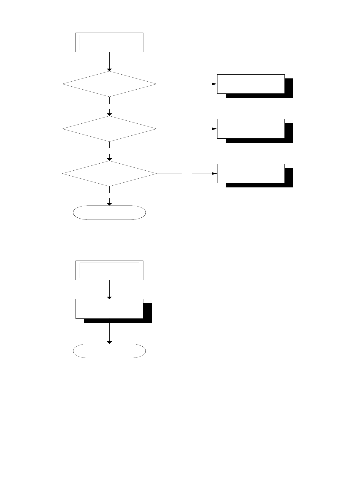
9. Trouble Shooting Guide
1. System trouble shooting :
Is LED light when
Main Power Switch
on?
n n
Check door luck
switch
1.Check +3Vs, +5Vs
2. Check power
Is Orange LED
active when remote
power on?
Is lamp turned on?
Does starting OSD
shows normally?
Does DVI-I signal
shows normally?
y
y
y
y
n
n
n
n
Are fans spinning?
Check DMD board
Check ballast
Check lamp
Does any stripe
shows on screen?
Check Connector
board and FPC
board
n
Check fans, wire and
Translation board
Check DMD board
y
Check DMD
socket
n
Check Main board, DMD
board
Does Video signal
shows normally?
y
n
Check Main board ,
FPC and Connector
board
39
Page 41
2. Main board trouble shooting:
Y
Y
Y
(1) Main:
REMOTE
POWERON
NO
ES
1. See CPU trouble shooting
U18, reset successful?
2. U17, RP25, RP24 OK?
3. CPU (U10) 56pin(IR) signal?
OSD ok?
When no valid
signal
OSD ok.
When input PC
signal
OSD ok.
When input
Video signal
NO
ES
NO
ES
NO
1. RP19,RP17,RP15,RP13
ok?
2. U19, U20 OK?
3. Check L8 with 100Mhz ok?
4. check L9 with 40Mhz ok?
1.check J2
1. RP1, RP2, RP3, RP4, R6
R3, R2, R4 ok? (SIL504
output)
2. check J2
Saving data in
EEPROM
YES
NO
1.Replace U6 (EEPROM)
2.check R36 R37(IIC pull high
resistors)
40
Page 42

Y
Y
Y
(2) SIL504 trouble shooting: (U4, U2)
X1, 20Mhz?
RESET
successful?
System IIC ok?
(U4 pin 15,14)
ES
SIL504 IIC ok?
(U4 pin 2, 3)
ES
DEINTDONE
Signal ok? (U4
pin21)
ES
No
No
No
No
1. check X1, C41, C42
2. check U17,RP25
1.Q2,Q3 ok? (level shift )
2. RP7 ok? ( IIC Pull high)
1. R10,R11ok? ( IIC Pull
high)
2. Replace U4
1. check SIL504 1.8V ok?
2. check U2, U3 ok?
41
Page 43

(3) CPU (U10) trouble shooting guide :
Check +3Vs
(pin92)
YES
Check X1
crystal
NO
1. Check C75, C76
2. replace X1
1. Check U9(SRAM), check CPU_LCS_N (pin 58) and
2. Check U12(Flash), check R68 and CPU_UCS_N (pin
YES
NO
RESET
Successful?
CPU_BHE_N is active?
57) is active?
YES
check U18, make sure U18
pin1 has delayed for certain
period of time ,from L go H.
42
Page 44

3. DMD board trouble shooting guide.
N
RESETZ And
POWERGOO
D?
Color wheel
Spinning?
Color wheel
Feedback (J3
pin3) ok?
Lamp light ok?
YES
YES
YES
O
NO
NO
NO
1. No RESETZ check main board and
translation board.
2. No POWERGOOD check main board
1. Check Color wheel and CW connector (J4)
2. CW power supply P12V of U13
1. Check CW sensor board and CW tag
2. Feedback 150Hz
1. Check J1 pin 1 (lampon) , normal status is
low
2. Check J1 pin 3(lamp light feedback) should
be low.
Normal Image
on screen ?
(32-Gray Pattern
in Factory mode
is
recommended)
YES
DMD pixels always on
Horizontal dark/bright lines
Check DMD socket.
Check C-spring
Check DMD B/D : DAD1000(U1) VCC (5V), VBIAS
(23 ~ 26V), VRST (-26V)
Vertical dark/bright lines
Check C-spring
Color missing
Check DMD socket.
43
Page 45

4. Connector board trouble shooting guide.
S-video is OK?
No
Composite is
No
OK?
Component is
No
OK?
Check L14,L17
Check U5
Check U10
Check L13
Check U5
Check U10
Check L15,L16,L18
Check U10
No
DVI- A is
OK?
DVI-D (HDCP)is
No
OK?
YPbPr is OK?
BNC-PC is OK?
No
No
J6 12V output?
Check L28,,L29,L31,L32,L33
Check U17
Check U18DDC
Check U17
Check L2,L3,L4
Check U2
Check U7
Check L2,L3,L4,L5,L6
Check U2,U3,U4
Check F1
Check Q2
Check L24
Check Q3
44
Page 46

RS232 is OK?
No
Check R61,R62
Check U14
Check main board
5. Power board trouble shooting guide.
Power BD Check.
Disconnect the wire
Fuse Broken ?
Yes
Proceed to "Prim ary
Circuit Check".
No
form b uttom b d . to
Short Pin12& P in9.
power bd.
No +3.3V Output.
Check + 3.3V-Fix exists ?
Yes
F704 Broken ?
Yes
Replace new fuse.
No
No
Check output
voltages.(1)+ 3.3V(2)
+1 2V (3 )+5 V (4)+ 5 V -
Fix(5)+3.3V-Fix.
Proceed to "No +3.3V-
Fix output".
Q 70 4 w o rk s no rm a lly ?
Yes
Check trace.
No
Check Q 702,Q703,
and O n/Off signal.
45
Page 47

N o +12V O utput
C heck 12V exists ?
Yes
Check Q703 works
norm ally ?(V ce<0.2V )
Yes
Check Q702 works
norm ally ?(V ce>10V )
Yes
C heck R 730 and
layout trace.
No +5V output.
C heck + 5V -F ix exist ?
No
No
No
No
Proceed to "N o 12V
Output".
Q 703 dam ages and
replace new
tran sistor.
Q 702 dam ages and
replace new
tran sistor.
Proceed to "No +5V -
Fix output".
Yes
Check Q701 works
norm ally ?(V ce<02V )
Yes
Check Q705 works
norm ally ?
Yes
C heck the trace of
+5V.
No
No
Q 701 dam ages and
replace new
tran sistor.
R eplace new P-
M O SFET.
46
Page 48
N o 12V output
o r N o + 5 V -F ix
output
C heck D 701 had been
inserted properly ?
Yes
C heck IC701 dam ages ?
No
C heck D 702 had been
inserted properly ?
Yes
Proceed to "Check
p rim a ry c irc uit" .
No
Yes
No
S o ld er it a g ain .
R eplace new IC 701.
S o ld er it a g ain .
No +3.3V-Fix
O utput
C heck IC705, IC602,
R 718, R 742, R 617,
Proceed to "Check
R616.
p rim a ry c irc uit" .
47
Page 49

Check primary
circ u it.
Fuse B roken ?
Yes
Yes
PinD & P inS of Q601
are shorted. Replace
new
R612,Q60 1,R611,ZD
602,IC601 and Fuse.
Check IC 601.
No
No
Proceed to "Check
IC601".
Check B D 651 dam ages ?Check Q601 dam ages ?
Yes
Inside diodes of
BD 601 are shorted.
Replace new bridge
diode.
No
Proceed to "Check
IC601".
Open R 612 an d inject
12V to Pin7 of
IC601.
Is the P W M w av efo rm o f
Pin6 of IC601 is correct ?
Yes
Replace ZD 601 and
IC603.
No
Replace IC601.
48
Page 50
10. Factory OSD Operation
There are 10 pages in this OSD, the ways to enter factory OSD are open user OSD, then
press power on button. If you have to return user OSD, open factory OSD and press power
on button again.
Go to \User OSD\Environment\lamp hours\minutes, then press Right, Left, Right, Left,
Enter in a row to switch to factory OSD.
1. Factory
This page is mostly for our factory to use.
Page Items Comment
Return User OSD
Save Settings
Load Saved Settings
Load Factory Default Load factory default
Load All User Default
Burn In Mode Burn-In mode On/Off
Factory
Burn In Timer Setup hours Set burn-in hours
Burn In Timer Running hours &
minutes
RS232 Baudrate Set baudrate of RS2329600 or 115200
Quit Factory OSD and return user OSD
Save current settings of factory OSD to EEPROM
Load previous saved settings from EEPROM
Restore all settings of user
OSD and PC/HD timing parameters
Running hours of burn-in mode
OSD Timer OSD automatic off time
Usage Hour Record total usage hours of this projector
Software version Software version
49
Page 51
2. HD Adj
This page is the settings of A/D converter. There are 2 sections, one is for RGBHV format
signal (DVI-A input and RGB-HD input), the other is for YPbPr format signal
(Comp-HD input).
Page Items Comment Range
Red Offset A/D converter red offset 0~127
Green Offset A/D converter green offset 0~127
Blue Offset A/D converter blue offset 0~127
RGBHV format
Red Gain A/D converter red gain 0~255
Green Gain A/D converter green gain 0~255
Blue Gain A/D converter blue gain 0~255
Page Items Comment Range
Brightness A/D converter green offset 0~127
Contrast A/D converter green gain 0~255
YPbPr format
3. STD Adj
This page is the settings of video decoder. There are 2 sections, one is for Video and
S-Video input, the other is for component input.
Page Items Comment Range
Saturation A/D converter red and blue gain 0~255
Pb-Offset A/D converter blue offset 0~127
Pr-Offset A/D converter red offset 0~127
Brightness V/D brightness 0~255
Contrast V/D contrast -128~127
Video & S-Video
Saturation V/D saturation -128~127
Hue V/D hue -128~127
50
Page 52
Page Items Comment Range
Brightness V/D brightness 0~255
Component
Contrast V/D contrast -128~127
Saturation V/D saturation -128~127
4. Color Balance
For color temperature settings, they are the combination of gamma gain and gamma
offset. This page allows operator to adjust gamma correction to fit the expected color
temperature, and save these settings as one of the color temperature settings. And this
page also provides the function to restore color temperature setting to default gamma
combination.
Page Items Comment Range
Red Adjust the shape of RM-1A gamma curve 0~128
Gamma
Green Adjust the shape of RM-1A gamma curve 0~128
Blue Adjust the shape of RM-1A gamma curve 0~128
Page Items Comment Range
Multiply gamma curve by a gain
1~512
(gain= settings/512)
Multiply gamma curve by a gain
1~512
(gain= settings/512)
Multiply gamma curve by a gain
1~512
(gain= settings/512)
Gamma Gain
Red
Green
Blue
Page Items Comment Range
Red Add an offset value to gamma curve 0~90
Gamma
Offset
Green Add an offset value to gamma curve 0~90
Blue Add an offset value to gamma curve 0~90
51
Page 53

Page Items Comment
Save Data Temp.
Page Items Comment
Save Video Temp.
Save gamma gain and gamm offset
as color temp 9300K
Save gamma gain and gamm offset
as color temp 6500K
Save gamma gain and gamm offset
as color temp 5700K
Restore combination
Save gamma gain and gamm offset as
color temp 9300K
Save gamma gain and gamm offset as
color temp 6500K
Save gamma gain and gamm offset as
For data input (Component >= 480p
signal, DVI-A, and DVI-D)
For data input (Component >= 480p
signal, DVI-A, and DVI-D)
For data input (Component >= 480p
signal, DVI-A, and DVI-D)
Restore default value of gamma
correction
For video input (Component < 480p
signal, Video, and S-Video)
For video input (Component < 480p
signal, Video, and S-Video)
For video input (Component < 480p
5. Filter Bypass
Page Items Comment
Filter Bypass
color temp 5700K
Restore combination
V-in
V-out On/Off status of RM-1A's video output filter
G-in On/Off status of RM-1A's graphics input filter
signal, Video, and S-Video)
Restore default value of gamma
correction
On/Off status of RM-1A's video input filter
52
Page 54

6. DLP
This page allows user to change DLP settings.
Page Items Comment Range
Brightness DLP brightness -64~64
Contrast DLP contrast 0~100
DLP
CW delay DLP color wheel delay 0~1023
Degamma
DLP degamma table 0~6
Table
7.Pattern1
This page allows user to call up DLP present curtains and RM-1A patterns.
Page Items Comment
Red Curtain
Green Curtain DLP present curtain. For CW delay measurement
Blue Curtain DLP present curtain. For CW delay measurement
Black Curtain DLP present curtain. For optical experiment.
Patterns 1
Color Bar RM-1A pattern. For checking gray scale.
DLP present curtain. For CW delay measurement
Checker Board RM-1A pattern. For optical contrast measurement.
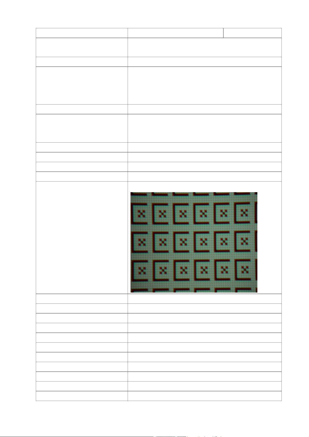
13-Points RM-1A pattern. For optical experiment.
Reflective Edge RM-1A pattern. For optical light leakage experiment
53
Page 55
8.Pattern2
This page allows user to call up DLP DDP1010 series present patterns.
Page Items Comment
Patterns 2
Solid Field - Yellow
Solid Field - Cyan
Solid Field - Magenta
Horizontal Ramp
Vertical Ramp
Horizontal Lines
Diagonal Lines DLP DDP1010 present pattern. Monochrome pattern.
Vertical Lines DLP DDP1010 present pattern. Monochrome pattern.
Grid
Checker Board DLP DDP1010 present pattern. Monochrome pattern.
DLP DDP1010 present pattern. For checking color.
DLP DDP1010 present pattern. For checking color.
DLP DDP1010 present pattern. For checking color.
DLP DDP1010 present pattern. Monochrome pattern,
for checking gray scale.
DLP DDP1010 present pattern. Monochrome pattern,
for checking gray scale.
DLP DDP1010 present pattern. Monochrome pattern.
DLP DDP1010 present pattern. Monochrome pattern.
9.Pattern3
This page allows user to call up DLP DDP1010 series present patterns, the major goal
of this page is for DMD inspection.
Page Items Comment
DLP DDP1010 present pattern. For inspection of 'major dark blemish' and
Patterns 3
Blue 90
'dark pixel' on DMD chip.
DLP DDP1010 present pattern. For inspection of 'border defects' on DMD
Gray 10
chip.
DLP DDP1010 present pattern. For inspection of 'major light blemish' and
Gray 6
light pixel' on DMD chip.
54
Page 56
White Full
Black Full
Red Ramp
DLP DDP1010 present pattern. For inspection of 'minor blemishes' on
DMD chip.
DLP DDP1010 present pattern. For inspection of 'minor blemishes' on
DMD chip.
DLP DDP1010 present pattern. For inspection of 'unstable pixel' on DMD
chip.
10 . Test Mode
For different situation, we need different settings. Here we define 5 kinds of settings in
‘Picture Adjust’ page to fit some situations.
Page Items Comment
Optical Test High brightness, high contrast, high saturation
Test Mode
Middle Value All settings in the middle value
Play DVD Optimal settings for watching DVD
Color Wheel Delay Low brightness, high contrast, high saturation
Blue Filter Only 'blue' is left, for 'color' and 'tint' adjustment
55
Page 57
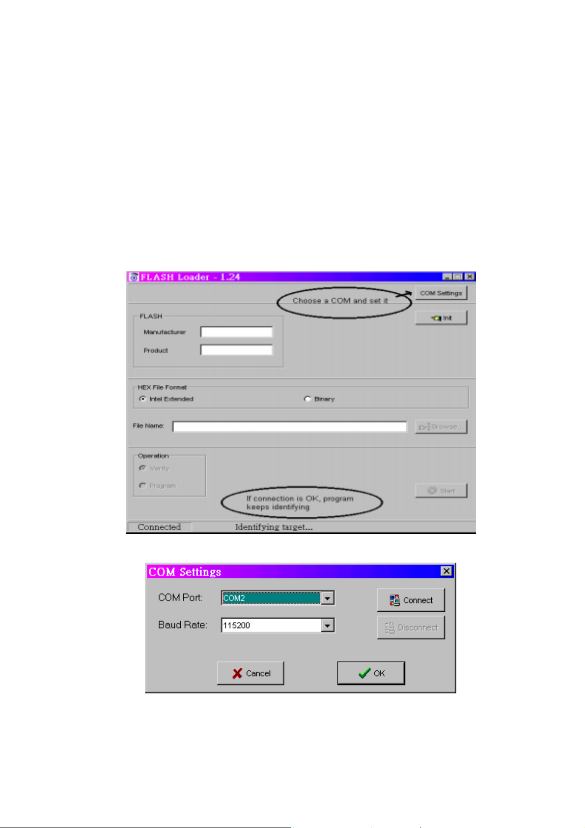
11. Firmware Upgrade Procedure
1. Connect specific download cable to RS232 (RJ-11) connector. Remember to turn the
AC switch off.
2. Execute the ‘Flash Loader’ program. If the ‘COM Settings’ item is ready, you can see
‘Identifying target…’ at the bottom of flash loader. If not, open ‘COM Settings’ item.
Choose the ‘COM Port’ you use, always set the baud rate 115200, then press ‘Connect’
and ‘OK’ button. The program returns to its main page, and ‘Connected’ and ‘Identifying
target’ are supposed to be displayed at the bottom of the flash loader.
56
Page 58

3. Turn the AC switch on. In 3 seconds, ‘flash loader’ will identify the flash ROM of this
unit. Choose ‘Hex File Format’ as ‘Intel Extended’, ‘Operation’ as ‘Program’, and
‘Browse’ the ‘File Name’. After that, press the ‘Start’ button. ‘Flash Loader’ starts to
load program to Flash ROM.
4. After download procedure finished, remove download cable and turn the AC switch off.
Then the user can operate this machine in normal condition.
5. The hex file to be loaded, the format of its name is
BenQ_PE8700_RM1A_Ver102_20030619.hex
I. II. III. IV. V.
I. Brand name
II. Model name
III. Scaler type
IV. Version of SW
V. Released date
57
Page 59

12. RS232 Codes
1. Set up peripherals
BenQ PE8700 provides an RJ-11 connector for RS232 serial communication control. The
user can use the ‘Hyper Terminal’ program of Microsoft Windows to control this unit.
To set the settings of serial port first is necessary. Choose which COM port you want
to connect, and set its settings as below:
Baud Rate: 115200 or 9600
Parity: None
Data bits: 8
Stop bits: 1
Flow Control: None
For baud rate setting, it depends on the settings in our \Factory OSD\FACTORY\RS232
BAUDRATE\ 9600 or 115200.
58
Page 60

After settling down, connect our specific RS232 cable and press the ‘call’ icon of ‘Hyper
Terminal’ program. After this, press ‘Enter’ key, if an ‘>’ symbol come up, that means the unit
is ready to accept commands for computer.
2. Commands list
There are 3 kinds of serial commands, X-group, Y-group and Z-group.
For X-group, these functions are public. Any end-user can control the unit by these
commands, as long as they set correct RS232 communication. Following table is the codes
list of X-group command.
59
Page 61

Code Function
X00 Must be Reversed , no function
X01 Power On
X02 Power Off
X03 Message On
X04 Message Off
X05 Lamp hours reset
X06 Load all user OSD default value
X07 Save current active source settings
X08 Change active OSD
X10 Menu
X11 Enter
X12 Exit
X13 Up(arrow key)
X14 Down(arrow key)
X15 Left(arrow key)
X16 Right(arrow key)
X20 Switch to Composite input
X21 Switch to S-Video input
X22 Switch to Component input
X23 Switch to Dsub_PC input
X24 Switch to YPbPr input
X25 Switch to BNC_PC input
X26 Switch to DVI input
X27 Switch to DVI_I input
X30 4:3 screen
X31 16:9 screen
X35 Aspect - Anamorphic
60
Page 62

X36 Aspect - Standard (4:3)
X37 Aspect - Letter box
X38 Aspect - Virtual wide
X39 Aspect - Through
X40 Load memory 1 settings
X41 Load memory 2 settings
X42 Load memory 3 settings
X43 Load 'optical test' mode settings
X44 Load 'middle' mode settings
X45 Load 'CW delay adjustment' mode settings
X46 Load default of current source
X47 Save memory 1 settings
X48 Save memory 2 settings
X49 Save memory 3 settings
X50 Scale up
X51 Scale down
X55 Switch active source
X56 Picture in picture display
X57 Picture by picture display
X60 Switch language 1
X61 Switch language 2
X62 Switch language 3
X63 Switch language 4
X64 Switch language 5
X65 Switch language 6
X66 Switch language 7
X67 Switch language 8
X85 PC input - auto
61
Page 63

X90 Image orientation - floor front
X91 Image orientation - ceiling front
X92 Image orientation - floor rear
X93 Image orientation - ceiling rear
X94 Back light board On
X95 Back light Board Off
X99 On line help
When an user sends a command, he must follow the command format in the list. After
he sends a command, program will acknowledge 2 pieces of information. This information,
we call it ‘ACK’ in the following content.
The format of first ACK is XnX
The length is 3, first and last characters are always be X. And the number ‘n’ is 0, 1 or
2. The explanation of n is
0: Right command format and function
1: Illegal format
2: Illegal function
So, if the user presses XA85, this one is wrong format, ACK will be X1X.
And if the user presses X98, because this function is not included in our command
table, ACK will be X2X.
For above situation, program sends the user an ACK, then waiting for a new
command.
If the user presses correct command, take an example, X35, first ACK, X0X will send
to the user. That tells the user it’s a right command. Then program starts to deal with this
command, and changes the aspect ratio to ‘anamorphic’ mode. When finish, the user will
receive 2nd ACK. The format is Xn_ccX
The length is 6. First and last characters are X, second character is the ACK, followed
by a ‘_’ character. ‘cc’ is the function number. So, in this case, the 2nd ACK is X0_35X. And
the user can continue to send next command.
For Y-group, this one is for our factory, not public. When our operators send
commands to the unit, the ACK format is identical as X-group, difference is only ‘Y’ instead
of ‘X’.
62
Page 64

Following is the list of Y-group:
Code Function
Y01 Save current factory settings
Y02 Load saved factory settings
Y03 Load factory default
Y04 Load all user default
Y05 Burn-In mode on
Y06 Burn-In mode off
Y07 Set RS232 baudrate as 9600
Y08 Set RS232 baudrate as 115200
Y10 Save as data color temperature 1
Y11 Save as data color temperature 2
Y12 Save as data color temperature 3
Y20 Save as video color temperature 1
Y21 Save as video color temperature 2
Y22 Save as video color temperature 3
Y30 Restore data color temperature to default
Y31 Restore video color temperature to default
Y32 Restore white balance settings to default
Y40 DMD -- Degamma table 0
Y41 DMD -- Degamma table 1
Y42 DMD -- Degamma table 2
Y43 DMD -- Degamma table 3
Y44 DMD -- Degamma table 4
63
Page 65

Y52 Red Curtain
Y53 Green Curtain
Y54 Blue Curtain
Y55 Black Curtain
Y57 Color Bar
Y58 Chess Board
Y59 Optical 13-point
Y60 Reflective Edge
Y61 Grid
Y62 Blue 90 Curtain
Y63 Gray 10 Curtain
Y64 Gray 6 Curtain
Y65 Full White Curtain
Y66 Full Black Curtain
Y67 Red Ramp Curtain
Y68 Gray 20 Curtain
Y70 Load 'optical test' mode settings
Y71 Load 'middle value' mode settings
Y72 Load 'Play DVD' mode settings
Y73 Load 'CW delay adjustment' mode settings
Y74 Load 'Blue filter' mode for color and tint adjustment
Y80 Load default for factory auto alignment procedure
Y81 Save corresponding settings after auto alignment
Y98 Display version
Y99 On line help
64
Page 66

Example:
1. Command = Y89893 (Enter)
ACK = Y1Y (Illegal format, wrong length)
2. Command = Y98 (Enter)
ACK = Y2Y (Illegal function)
3. Command = Y52 (Enter)
st
ACK = Y0Y
1
2nd ACK = Y0_52Y
For Z-group, this one is for ‘auto-alignment’ procedure in our factory. This one allows
engineers to read or write the unit settings without OSD operation, it will save time to set
the value. Following is the table of Z-group.
Code Function
Z001 Brightness adjustment
Z002 Contrast adjustment
Z003 Color adjustment
Z004 Sharpness adjustment
Z005 Tint adjustment
Z006 Color temperature adjustment
Z007 Filters adjustment
Z008 Independent color control - Red adjustment
Z009 Independent color control - Green adjustment
Z010 Independent color control - Blue adjustment
Z011 Independent color control - Yellow adjustment
Z012 DMD white peaking adjustment
Z020 Frequency adjustment
Z021 Phase adjustment
Z022 H - Position adjustment
Z023 V - Position adjustment
65
Page 67

Z030 Keystone adjustment
Z034 RGBHV input -- Red offset
Z035 RGBHV input -- Green offset
Z036 RGBHV input -- Blue offset
Z037 RGBHV input -- Red gain
Z038 RGBHV input -- Green gain
Z039 RGBHV input -- Blue gain
Z042 YPbPr input -- Brightness
Z043 YPbPr input -- Contrast
Z044 YPbPr input -- Saturation
Z045 YPbPr input -- Pb Offset
Z046 YPbPr input -- Pr Offset
Z050 CVBS & S-Video -- Brightness
Z051 CVBS & S-Video -- Contrast
Z052 CVBS & S-Video -- Saturation
Z053 CVBS & S-Video -- Hue
Z054 Component -- Brightness
Z055 Component -- Contrast
Z056 Component -- Saturation
Z060 Gamma--Index
Z061 Gamma--Red
Z062 Gamma--Green
Z063 Gamma--Blue
Z064 Gamma gain -- Red
Z065 Gamma gain -- Green
Z066 Gamma gain -- Blue
Z067 Gamma offset -- Red
Z068 Gamma offset -- Green
66
Page 68

Z069 Gamma offset -- Blue
Z070 DMD -- Brightness
Z071 DMD -- Contrast
Z072 DMD -- Color Wheel Delay
Z073 DMD -- Degamma table
Z080 Burn-in hours
Z099 On line help
The length of the command must be 11. The format, take an example, to read DMD
color wheel delay:
Z072RxxxxxZ, where
Byte 1: must be 'Z' or 'z'
Byte 2~4: function code
Byte 5: action, must be ‘r’ or ‘R’
Byte 6~10: Don’t care
Byte 11: must be 'Z' or 'z'
In contrast, if write DMD color wheel delay:
Z072W+0025Z, where
Byte 1: must be 'Z' or 'z'
Byte 2~4: function code
Byte 5: action, must be ‘w’ or ‘W’
Byte 6: sign byte, must be ‘-‘ or ‘+’
Byte 7~10: the value to be written
Byte 11: must be 'Z' or 'z'
67
Page 69

And the length of ACK must be 12, and format is
Z0_072+0025Z
Byte 1: Always ‘Z’
Byte 2: ACK
Byte 3: Always ‘_’
Byte 4~6: function code
Byte 7: sign byte, ‘+’ or ‘-‘
Byte 8~11: the current value after writing
Byte 12: Always ‘Z’
And ‘ACK’ value is
0: Right command and function
1: Illegal Format
2: Illegal Function
3: Illegal Action,
4: Illegal Adjusted Situation,
5. Written value is over up limit,
6. Written value is over down limit
If the ACK is 0, 5, 6, program will deal this command. If ACK = 5, program writes the legal
maximum value to the setting. If ACK = 6, writes the legal minimum value to the setting.
68
Page 70
5
120-Pin B2B Connectors
D D
C C
TP7
E1
1
SII141_PDO
B B
A A
TRIGGER
RM1_RST_N
MUX_SEL
+12VA +3VA+5VA+5VS +1_8V
SPAREI
SPAREO
SII141_PDO
TRIGGER
RM1_RST_N
MUX_SEL
SPAREI
SPAREO
+3VA
+5VA
+12VA
+1_8V
+5VS
1_120Pin B2B Connectors
5
D_INA[0..23]
D_VSYNC
D_HSYNC
DIN_CLK
DVI_SCDT
DI_IN[2..9]
DI_27M_CLK
DI_VSYNC
DI_HSYNC
CPU_RXD0
CPU_TXD0
MUX_SEL_P
MUX_BUFFER
DVI_ACTDATA
MUX_SEL_Q
DVI_SCDT
+3VA
DI_IN[2..9]
DI_27M_CLK
DI_VSYNC
DI_HSYNC
+1_8V+3VA
DEINTDONE
RESET_DVDO
TP20
TP18
TP19
E1
E1
E1
1
1
1
SCL
SDA
IR
1
1
TP8
TP9
E1
E1
+5VA+3VA
TP17
E1
1
1
TP15
E1
D_INA[0..23]
D_VSYNC
D_HSYNC
DIN_CLK
+3VA
8_SDRAM 64MBit x 3
SDRAM 64MBit x 3
Sil503_Deinterlacer
DI_IN[2..9]
DI_27M_CLK
DI_VSYNC
DI_HSYNC
RESET_DVDO
DEINTDONE
+1_8V
+3VA
2_Sil504_Deinterlacer
MCU503 Controller
DEINTDONE
+5VA
+3VA
3_MCU503 Controller
4
4
MEM_DQ[0..79]
MEM_A[0..11]
MEM_RAS_N
MEM_CAS_N
MEM_BS
MEM_CLK
MEM_WE_N
MEM_CS_N
MEM_DQM_L
MEM_DQM_U
V_IN[0..15]
V_ACTIVE
V_VSYNC
V_HSYNC
VCLK
DI_SDA
DI_SCL
DI_SCL
DI_SDA
MCURESETRESET_DVDO
DMD_SDA
DMD_SCL
3
TP4
TP2
TP3
TP1
E1
E1
E1
E1
SCL
SDA
CPU_RXD0
CPU_TXD0
MUX_SEL_P
MUX_BUFFER
MUX_SEL_Q
IR
3
TP11
E1
CPU_A1
CPU_A2
CPU_A3
CPU_A4
MCURESET
TRIGGER
SII141_PDO
MUX_SEL
DVI_SCDT
RM1_RST_N
1
CPU_RD_N
CPU_D[0..7]
CPU_A[0..7]
RM1_WR_N
RM1CLKIN
RM1_CS_N
RM1_IRQ
1
1
+12VA +5VS+3VA +3VS+5VA
CPU_D[0..7]
1
1
OP_A[0..23]
OP_VSYNC
OP_HSYNC
OP_ENABLE
OCLK_OUT
OP_FIELD
+3VS
CPU_RD_N
CPU_FLASH_SRAM
CPU_RD_N
CPU_D[0..7]
CPU_A[0..7]
RM1_WR_N
RM1CLKIN
RM1_CS_N
RM1_IRQ
SCL
SDA
CPU_RXD0
CPU_TXD0
MUX_SEL_P
MUX_BUFFER
BACKLIGHT_CTRL
MUX_SEL_Q
IR
5_CPU_FLASH_SRAM
80 Pin Connector to DLP
OP_A[0..23]
OP_VSYNC
OP_HSYNC
OP_ENABLE
OCLK_OUT
OP_FIELD
+5VS
+3VS
+12VA
+5VA
+3VA
I/O
CPU_A1
CPU_A2
CPU_A3
CPU_A4
MCURESET
TRIGGER
SII141_PDO
MUX_SEL
DVI_SCDT
RM1_RST_N
+3VS
CPU_RD_N
CPU_D[0..7]
6_I/O
SPAREI
SPAREI
SPAREO
SPAREO
CPU_PCS0_N
CPU_WR_N
CPU_PCS0_N
CPU_WR_N
CPU_WR_N
CPU_PCS0_N
DLP_SPARE
DLP_SPARE
DLP_SPARE
RESETVCC
RESETVCC
WRITE_PROT
RESETVCC
RESET_N
WRITE_PROT
RESET_N
RESET_N
WRITE_PROT
RM1
D_INA[0..23]
D_VSYNC
D_HSYNC
DIN_CLK
MEM_DQ[0..79]
MEM_A[0..11]
MEM_RAS_N
MEM_CAS_N
MEM_BS
MEM_CLK
MEM_WE_N
MEM_CS_N
MEM_DQM_L
MEM_DQM_U
V_IN[0..15]
V_ACTIVE
V_VSYNC
V_HSYNC
V_CLK
DI_SCL
DI_SDA
MCURESET
DMD_SDA
DMD_SCL
SCL
SCL
SDA
SDA
DVI_ACTDATA
+1_8V
MEM_DQ[0..79]
MEM_A[0..11]
MEM_RAS_N
MEM_CAS_N
MEM_BS
MEM_CLK
MEM_WE_N
MEM_CS_N
MEM_DQM_L
MEM_DQM_U
V_IN[0..15]
V_ACTIVE
V_VSYNC
V_HSYNC
VCLK
+3VA
+3VA
+1_8V
4_RM1
DVI_ACTDATA
OP_A[0..23]
OP_VSYNC
OP_HSYNC
OP_ENABLE
OCLK_OUT
OP_FIELD
RM1_RST_N
CPU_RD_N
CPU_D[0..7]
CPU_A[0..7]
RM1_WR_N
RM1CLKIN
RM1_CS_N
RM1_IRQ
BACKLIGHT_CTRL
2
DLP
Connector/POWER
SYNCVALID
BALLAST_CTRL
TP6
E1
POWERON
POWERON
KEYPAD[0..9]
1
SYNCVALID
BALLAST_CTRL
SYNCVALID
BALLAST_CTRL
LAMP_PROTECT
BACKLIGHT_CTRL
SYNCVALID
BALLAST_CTRL
LAMP_PROTECT
TP16
E1
1
CPU
2
POWERON
DLP_RESETZ
KEYPAD[0..9]
SCL
SDA
DLP_RESETZ
TP13
E1
1
DLP_RESETZ
POWERON
KEYPAD[0..9]
LAMP_PROTECT
SCL
SDA
BACKLIGHT_CTRL
KEY_LED2
FAN_CTRL
KEY_LED2
FAN_CTRL
KEY_LED2
FAN_CTRL
DMD_SCL
DMD_SDA
POWER
LAMPLIT
7_100 Pin Connector to DLP/POWE
KEYPAD&THERMAL_CONNECTOR
+3VS
+5VS
KEY_LED1
KEY_LED0
KEY_LED1
KEY_LED1
KEY_LED0
KEY_LED0
DMD_SCL
DMD_SDA
+12VA
DLP_RST
10_KEYPAD&THERMAL_CONNECTOR
DLP_RST
DLP_RST
LAMPLIT
POWER
+12VA
+5VA
+12VA
+5VA
+5VS
+3VA
+3VS
Benq Corporation
Project Code
99.J5877.001
Title
Size Document Number R e v.
PCB P/N
<Size>
Thursday, January 16, 2003
Date: Sheet
Prepared By
ANGEL HU
IR
LAMPLIT
POWER
+5VS
DMD_SCL
DMD_SDA
POWER
LAMPLIT
IR
+3VS
+3VA
48.J5801.S02
1
+5VS+3VS +12VA
Model Name
MAIN BOARD
1
TP5
E1
1
POWER
OEM/ODM Model Name
HT720G
PCB Rev.
99.J5877.R22-C3-304-001
S02
Reviewed By Approved By
COLIN CHANG B EN CHEN
NA
of
1
0
10
Page 71
5 4 3 2 1
D
+5VS
+5VS
C1
0.1UF
+12VA
J1
1
2
3
4
5
6
7
10
11
12
13
14
15
16
17
18
19
20
CON20
8
9
C
BACK_LIGHT_CTRL
KEYPAD0
KEYPAD1
KEYPAD2
KEYPAD3
KEYPAD4
KEYPAD5
KEYPAD6
KEYPAD7
KEYPAD8
KEYPAD9
KEY_LED0
KEY_LED1
KEY_LED2
IR
KEYPAD[0..9]
+12VA
LAMP_PROTECT
+3VS
SDA
SCL
FAN_CTRL
DLP_RST
POWERON
DLP_RESETZ
+3VS
SDA
SCL
1
2
3
4
5
6
7
8
9
10
11
12
CON_12P
J5
1
2
3
4
5
6
7
8
9
10
11
12
THERMAL CONNECTOR
B
BACKLIGHT_CTRL
A
KEYPAD CONNECTOR
+3VS
147
12
13
11
U8D
74HC132
BACK_LIGHT_CTRL
Benq Corporation
Project Code
99.J5877.001
Title
Size Document Number Re v.
PCB P/N
<Size>
Date: Sheet
48.J5801.S02
Thursday, January 16, 2003
Prepared By
ANGEL HU
Model Name
HT720G
MAIN BOARD
PCB Rev.
S02
Reviewed By Approved By
COLIN CHANG BEN CHEN
OEM/ODM Model Name
99.J5877.R22-C3-304-001
2
NA
10
of
0
Page 72
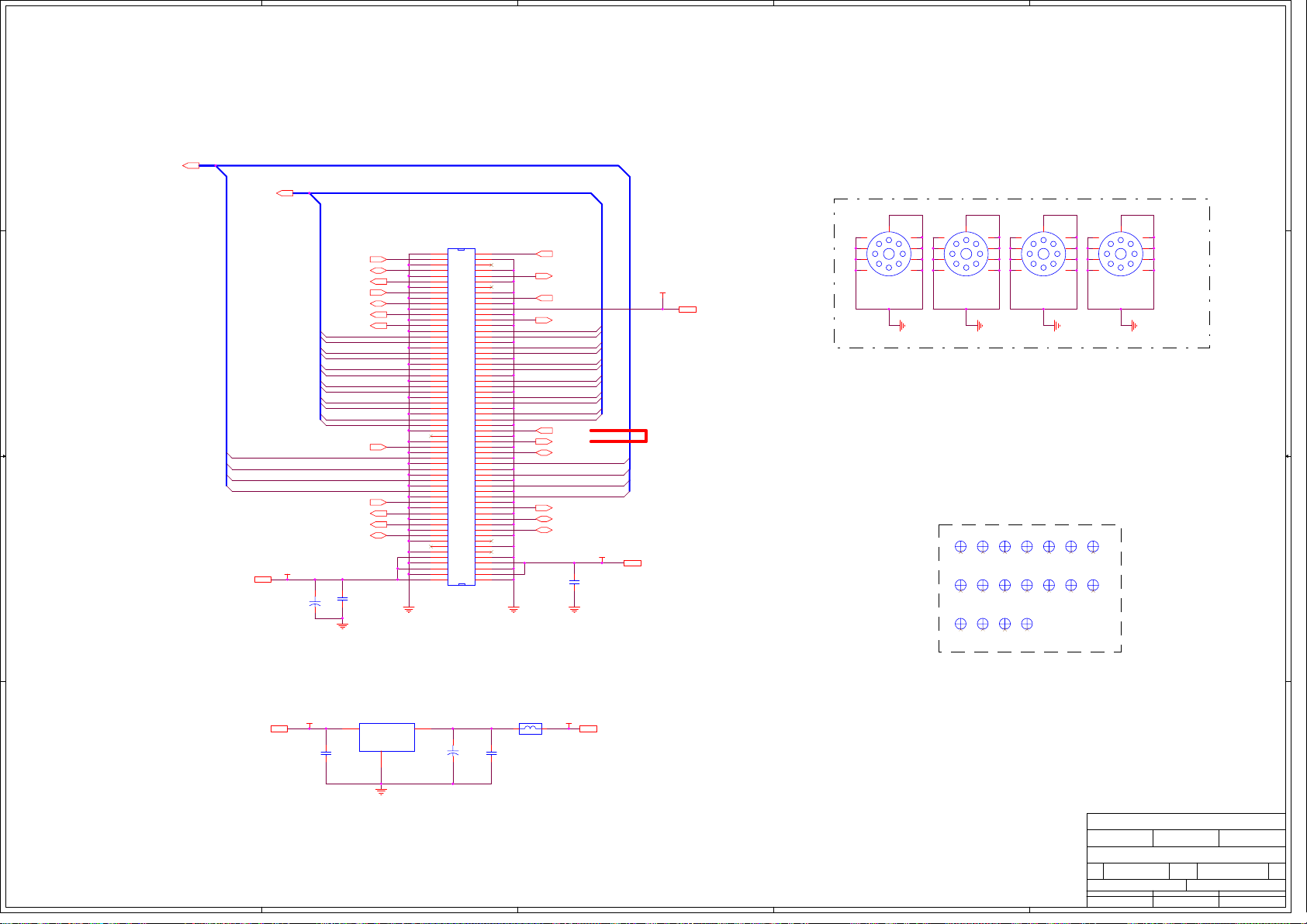
5
D D
DI_IN[2..9]
D_INA[0..23]
RED -- D_INA[23..16]
GREEN -- D_INA[15..8]
BLUE -- D_INA[7..0]
MUX_SEL_P
CPU_RXD0
CPU_TXD0
MUX_BUFFER
D_HSYNC
D_INA21
C C
B B
+5VA
+5VA
C3
10UF/16
D_INA20
D_INA17
D_INA16
D_INA13
D_INA12
D_INA9
D_INA8
D_INA5
D_INA4
D_INA1
D_INA0
DI_IN8
DI_IN6
DI_IN4
DI_IN2
RM1_RST_N
DI_HSYNC
DI_27M_CLK
+
TRIGGER
DIN_CLK
SPAREO
C4
0.1UF
4
3
2
1
Screw Holes
1
5
J2
1
61
1
61
2
62
2
62
3
63
3
63
4
64
4
64
5
65
5
65
6
66
6
66
7
67
7
67
8
68
8
68
9
69
9
69
10
70
10
70
11
71
11
71
12
72
12
72
13
73
13
73
14
74
14
74
15
75
15
75
16
76
16
76
17
77
17
77
18
78
18
78
19
79
19
79
20
80
20
80
21
81
21
81
22
82
22
82
23
83
23
83
24
84
24
84
25
85
25
85
26
86
26
86
27
87
27
87
28
88
28
88
29
89
29
89
30
90
30
90
31
91
31
91
32
92
32
92
33
93
33
93
34
94
34
94
35
95
35
95
36
SCL
96
97
98
99
100
101
102
103
104
105
106
107
108
109
110
111
112
113
114
115
116
117
118
119
120
36
96
37
97
38
98
39
99
40
100
41
101
42
102
43
103
44
104
45
105
46
106
47
107
48
108
49
109
50
110
51
111
52
112
53
113
54
114
55
115
56
116
57
117
58
118
59
119
60
120
AMP 120P D0.8
37
38
39
40
41
42
43
44
45
46
47
48
49
50
51
52
53
54
55
56
57
58
59
60
DVI_SCDT
IR
MUX_SEL
D_VSYNC
D_INA23
D_INA22
D_INA19
D_INA18
D_INA15
D_INA14
D_INA11
D_INA10
D_INA7
D_INA6
D_INA3
D_INA2
SII141_PDO
DVI_ACTDATA
SDA
DI_IN9
DI_IN7
DI_IN5
DI_IN3
DI_VSYNC
SPAREI
MUX_SEL_Q
C2
0.1UF
+12VA
+5VS
+5VS
SPARE for DVI interface
+12VA
4
3
2
H1
HOLE-V8
9
8
7
6
1
5
4
3
2
H2
HOLE-V8
Optical Points
OP1
OP
OP8
OP
OP15
OP
9
8
7
6
OP2
OP
OP9OPOP10
OP
OP16
OP
5
4
3
2
H3
HOLE-V8
OP3
OP4OPOP5OPOP6OPOP7
OP
OP
OP11OPOP12OPOP13
OP
OP17
OP18
OP
OP
1
9
8
7
6
OP14
OP
5
4
3
2
H4
HOLE-V8
1
9
8
7
6
U1
LM8117A-1.8(SOT223)
3
C6
0.1UF
VIN
GND
1
4
+3VA
A A
5
VOUT
+1.8VOUT
2
C5
+
22UF/16
C7
0.1UF
L1
112
FCB3216K
+1_8V+3VA
2
+1_8V
Benq Corporation
Project Code
99.J5877.001
Title
Size Document Number R e v.
PCB P/N
<Size>
Thursday, January 16, 2003
Date: Sheet
Prepared By
3
2
ANGEL HU
Model Name
MAIN BOARD
48.J5801.S02
1
OEM/ODM Model Name
HT720G
PCB Rev.
99.J5877.R22-C3-304-001
S02
Reviewed By Approved By
COLIN CHANG B EN CHEN
NA
of
3
0
10
Page 73
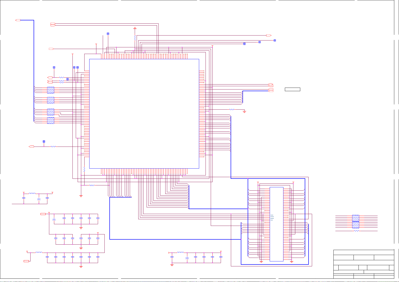
5
4
3
2
1
V_IN[0..15]
D D
C C
B B
A A
V_IN[0..15]
VCLK
Note: For compatability with Sil504
place bypass resistors
VDD_CORE
C8
0.1UF
AVSSI
+1_8V
+1_8V
RESET_DVDO
V_IN0
V_IN1
V_IN2
V_IN3
V_IN4
V_IN5
V_IN6
V_IN7
V_IN8
V_IN9
V_IN10
V_IN11
V_IN12
V_IN13
V_IN14
V_IN15
TP29
VCLK
L2
Z1000/100MHZ
+3VA
L3 Z1000/100MHZ
DI_VSYNC
DI_HSYNC
V_ACTIVE
V_VSYNC
V_HSYNC
RP1 47_RP
RP2 47_RP
RP3 47_RP
RP4 47_RP
E1
1
PLL Power
+
C9
10UF/16
TP25
+3VA
E1
R6 33
VDD_PLL
C10
0.1UF
C23
4.7UF/16
1
12
34
56
78
12
34
56
78
12
34
56
78
12
34
56
78
+
R2 33
R3 33
R4 33
C11
10UF/16
C17
0.1UF
C24
0.1UF
CB0
CB1
CB2
CB3
CB4
CB5
CB6
CB7
GREEN_Y2
GREEN_Y3
GREEN_Y4
GREEN_Y5
GREEN_Y6
GREEN_Y7
GREEN_Y8
GREEN_Y9
0.1UF
0.1UF
0.1UF
RESET_DVDO
+3VA
TP26
E1
TP28
503CBLANK
E1
V_CSYNC
1
503VSYNC
503HSYNC
VIDOUTCLK
C12
C18
C25
1
C13
0.1UF
C19
0.1UF
C26
0.1UF
DI_VSYNC
DI_HSYNC
TP27
E1
1
EXTREFSEL
R99
NC_R0603
C14
0.1UF
C20
0.1UF
C27
0.1UF
1
NC
2
VDDCORE_1.8
3
GND
4
LCDPWREN
5
/CBLANK
6
/CSYNC
7
/VSYNC
8
/HSYNC
9
BLUE_CB0
10
BLUE_CB1
11
BLUE_CB2
12
BLUE_CB3
13
BLUE_CB4
14
BLUE_CB5
15
GND
16
VDD
17
BLUE_CB6
18
BLUE_CB7
19
BLUE_CB8
20
BLUE_CB9
21
GND
22
GREEN_Y0
23
GREEN_Y1
24
GREEN_Y2
25
GREEN_Y3
26
VDD
27
GREEN_Y4
28
GREEN_Y5
29
GREEN_Y6
30
GREEN_Y7
31
GREEN_Y8
32
GREEN_Y9
33
GND
34
RED_CR0
35
RED_CR1
36
RED_CR2
37
RED_CR3
38
RED_CR4
39
RED_CR5
40
GND
41
VDDCORE_1.8
42
RED_CR6
43
RED_CR7
44
RED_CR8
45
RED_CR9
46
VIDOUTCLK
47
GND
48
/BYPPLLCLK48M
49
CLK48M
50
GND
51
VDDCORE_1.8
52
ExtRefSel_N
R98 4.7K
0.1UF
0.1UF
0.1UF
TP21
E1
197
199
198
196
GND
WSLN
SCKLN
VDDCORE_1.8
A4
A5
A7
A6
R1
10K
192
195
193
189
194
191
190
VDD
GND
SDLN
SDOUT
WSOUT
SCKOUT
A9
A8
A11
A10
1
AVSSI
VDD_PLL
CLK54_72M
205
203
207
208
201
202
206
200
204
GND
TEST0
TEST1
/RESET
AVSS_1.8
AVDD_1.8
CLK54_72M
VDDCORE_1.8
/BYPPLLCLK54_72M
EXTREFCLKXTALIN
GND55VDDCORE_1.856MEMADDR357MEMADDR258MEMADDR159MEMADDR060GND61MEMADDR462MEMADDR563MEMADDR664MEMADDR765GND66MEMADDR867MEMADDR968MEMADDR1069MEMADDR1170RSVD71GND72VDD73VDD74/RAS75/CAS76/WE77DQM78GND79MEMDATA780MEMDATA582MEMDATA4
ExtRefClkXtalOut
54
53
A3
A1
A0
A2
C15
C16
0.1UF
VDD_CORE
C22
C21
0.1UF
C28
C29
0.1UF
187
186
188
VDD
MEMADDR12
DEINTDONE_N
RASN
176
177
178
179
180
181
174
183
184
185
/DET32PD
/DET22PD
/DETVIDEO
U2
SII504
DQM
CASN
WEN
182
VDD
GND
173
175
HOSTDATA5
HOSTDATA4
HOSTDATA3
HOSTDATA2
HOSTDATA1
HOSTDATA0
HOSTDATA7 / VS
HOSTDATA6 / HS
MEMDATA681MEMDATA384GND85MEMDATA286MEMDATA187MEMDATA088VDD89PUPDIS90MEMDATA891MEMDATA992GND93MEMDATA1094MEMDATA1195MEMDATA1296MEMDATA1397MEMDATA1498VDDCORE_1.899GND
83
DQ0
DQ2
DQ3
DQ6
DQ7
DQ1
DQ5
DQ4
164
165
166
169
170
168
171
172
167
GND
RSVD
VDDCORE_1.8
HOSTDATA9 / VIDLNDATA13
HOSTDATA8 / VIDLNDATA12
HOSTDATA14 / VIDLNDATA18
HOSTDATA13 / VIDLNDATA17
HOSTDATA12 / VIDLNDATA16
HOSTDATA11 / VIDLNDATA15
HOSTDATA10 / VIDLNDATA14
DQ8
DQ10
DQ9
Z1000/100MHZ
+3VA
C34
0.1UF
163
160
161
162
159
157
158
GND
HOSTCLK
HOSTMODE
HOSTADDR6
HOSTADDR7
VDDCORE_1.8
HOSTADDR5
HOSTADDR4
HOSTADDR3
HOSTADDR2
HOSTADDR1
HOSTADDR0
HOSTDATA15 / VIDLNDATA19
/HOSTCS
/HOSTRD_SDA
/HOSTWR_SCL
VDDCORE_1.8
VIDLNCLK
VIDLNDATA9
VIDLNDATA8
VIDLNDATA7
VIDLNDATA6
VIDLNDATA5
VIDLNDATA4
VIDLNDATA3
VIDLNDATA2
RSVD
RSVD
MEMDATA16
MEMDATA17
MEMDATA18
MEMDATA19
MEMDATA20
MEMDATA21
MEMDATA22
MENDATA23
MEMDATA31
MEMDATA30
MEMDATA29
MEMDATA28
MEMDATA27
MEMDATA26
MEMDATA25
MEMDATA24
MEMDATA15
/BYPPLLMEMCLK
VDDCORE_1.8
MEMCLK
GND
RSVD
100
101
102NC103
104
DQ14
DQ13
DQ12
DQ11
L5
+
C35
10UF/16
DEINTDONE
INTERLACE_DETECT
2:2_DETECT
DI_RSVD1
DQ[0..31]
+3V_MEM
C38
0.1UF
DQ16
DQ18
DQ19
DQ20
DQ21
DQ22
DQ23
DQ31
DQ28
DQ27
DQ25
DQ26
DQ24
DQ15
M_CLK
DQ17
DQ29
DQ30
A[0..11]A[0..11]
C39
0.1UF
3:2_DETECT
DI_IN9
DI_IN8
DI_IN7
DI_IN6
DI_IN5
DI_IN4
DI_IN3
DI_IN2
VDD_CORE
156
155
154
153
152
151
150
GND
149
148
147
146
145
144
GND
143
142
141
140
139
138
137
136
135
VDD
134
133
132
VDD
131
GND
130
129
128
127
126
GND
125
124
123
122
121
GND
120
119
118
GND
117
VDD
116
115
114
GND
113
112
111
110
109
108
107
GND
106
105
NC
C37
C36
0.1UF
0.1UF
R5 10K
TP24
1
E1
DI_SDA
DI_SCL
DI_27M_CLK
DI_IN[2..9]
TP23
1
E1
Note: The Sil 503 does not support a standard
I2C protocol. See data sheet page 22.
+3VA
DQ0
DQ1
DQ2
DQ3
DQ4
DQ5
DQ6
DQ7
DQM
WEN
CASN
RASN
A11
A12
A10
A0
A1
A2
DQ16
DQ17
DQ18
DQ19
DQ20
DQ21
DQ22
DQ23
DEINTDONE
TP22
1
E1
DI_SDA
DI_SCL
DI_27M_CLK
DI_IN[2..9]
DQ[0..31]
1
VDD
2
DQ0
3
VDDQ
4
DQ1
5
DQ2
6
VSSQ
7
DQ3
8
DQ4
9
VDDQ
10
DQ5
11
DQ6
12
VSSQ
13
DQ7
14
NC
15
VDD
16
DQM0
17
WE
18
CAS
19
RAS
20
CS
21
NC
22
BA0
23
BA1
24
A10/AP
25
A0
26
A1
27
A2
28
DQM2
29
VDD
30
NC
31
DQ16
32
VSSQ
33
DQ17
34
DQ18
35
VDDQ
36
DQ19
37
DQ20
38
VSSQ
39
DQ21
40
DQ22
41
VDDQ
42
DQ23
VDD43VSS
K4S643232C-TC/L10
Input Port
+3V_MEM
U3
86
DQ15
VSSQ
DQ14
DQ13
VDDQ
DQ12
DQ11
VSSQ
DQ10
VDDQ
DQM1
DQM3
DQ31
VDDQ
DQ30
DQ29
VSSQ
DQ28
DQ27
VDDQ
DQ26
DQ25
VSSQ
DQ24
VSS
DQ9
DQ8
NC
VSS
NC
NC
CLK
CKE
A9
A8
A7
A6
A5
A4
A3
VSS
NC
DQ15
85
84
DQ14
83
DQ13
82
81
DQ12
80
DQ11
79
78
DQ10
77
DQ9
76
75
DQ8
74
73
72
DQM
71
70
69
M_CLK
68
67
A9
66
A8
65
A7
64
A6
63
A5
62
A4
61
A3
60
59
58
57
DQ31
56
55
DQ30
54
DQ29
53
52
DQ28
51
DQ27
50
49
DQ26
48
DQ25
47
46
DQ24
45
44
Note: Connect RP4, RP5 and R256 to bypass Sil503
V_IN8
1 2
V_IN9
RP5
NC_RP
RP6
NC_RP
Benq Corporation
Project Code
Title
Size Document Number R e v.
<Size>
Date: Sheet
3 4
V_IN10
5 6
V_IN11
7 8
V_IN12
1 2
V_IN13
3 4
V_IN14
5 6
V_IN15
7 8
VCLK
99.J5877.001
PCB P/N
48.J5801.S02
Thursday, January 16, 2003
Prepared By
ANGEL HU
R7 NC_R0603
Model Name
MAIN BOARD
DI_IN2
DI_IN3
DI_IN4
DI_IN5
DI_IN6
DI_IN7
DI_IN8
DI_IN9
DI_27M_CLK
OEM/ODM Model Name
HT720G
PCB Rev.
99.J5877.R22-C3-304-001
S02
Reviewed By Approved By
COLIN CHANG BEN CHEN
NA
0
of
10
4
Page 74

5
D D
4
3
2
1
RESET_DVDO
DMD_SDA
DMD_SCL
MCURESET
C C
SDA
SCL
DEINTDONE
B B
R120
R121
0
0
(open)
(open)
+5VA
+3VA
1
Q2
2
1
Q3
2
BSN20
BSN20
3
+3VA
1
Q1
3
2
BSN20
3
12
34
56
RP8 4.7K_RP
RP9 4.7K_RP
78
12
34
56
78
123456
+5VA
78
RP7
4.7K_RP
RESET_DVDO
SDA_5V
SCL_5V
DEINTDONE
R13 10M
X1 20 MHZ
C41
22PF
+5VA
MCEN
MCADDRSEL
FILM
SUBT
GAME
EXTGAME
CLKSPEED
YPBPR
24
13
PICXIN
PICXOUT
C42
22PF
1
15
14
21
6
7
5
4
11
12
13
25
26
28
9
10
U4
DVRESET
SDA
SCL
VSYNC
ENABLE
SA
FILMBIAS
SUBTITLE
GMODE
EXTGMD
MCKSEL
SQMODE
YPRPB
WAVE
OSC1
OSC2
MCU503
3
D
1
G2S
BSN20
PRMODE0
PRMODE1
VDD
DVSDA
DVSCL
GPIO0
GPIO1
RSVD0
+5VA
R8
R9
470
LED1_EN
12
470
LED2_EN
12
D2
LED_1206
+5VA
C40
0.1UF
20
DI_SDA
2
DI_SCL
3
LED0
23
LED1
24
22
27
18
RX
17
TX
16
19
Vss
8
Vss
R10
2.2K
R11
2.2K
D1
LED_1206
DI_SDA
DI_SCL
LED2 LED3 SOURCE
ON ON 3:2
ON OFF 2:2
OFF ON VID
OFF OFF GAME
A A
5
4
3
2
Benq Corporation
Project Code
99.J5877.001
Title
Size Document Number Rev.
PCB P/N
<Size>
Thursday, January 16, 2003
Date: Sheet
Prepared By
ANGEL HU
48.J5801.S02
Model Name
HT720G
MAIN BOARD
PCB Rev.
S02
Reviewed By Approved By
COLIN CHANG BEN CHEN
OEM/ODM Model Name
99.J5877.R22-C3-304-001
5
1
NA
10
of
0
Page 75

5
4
3
2
1
MEM_DQ[0..79]
VCLK
V_HSYNC
V_ACTIVE
CPU_RD_N
RM1_CS_N
V_VSYNC
RED -- D_INA[23..16]
GREEN -- D_INA[15..8]
BLUE -- D_INA[7..0]
V_IN[0..15]
+3VA
R28
R27
1K
1K
+1_8V
+3VA
D_INA[0..23]
CPU_D[0..7]
CPU_D0
R1633
R1733
OP_FIELD
RM1CLKIN
R20 NC_R0603
+3VA
RM1_IRQ
OP_A23
OP_A21
OP_A20
OP_A22
RP10 47_RP
OP_A18
OP_A19
OP_A14
RP11 47_RP
OP_A15
OP_A16
OP_A10
OP_A12
OP_A11
RP12 47_RP
OP_A13
OP_A6
OP_A7
RP14 47_RP
OP_A9
OP_A4
OP_A8
OP_A3
RP16 47_RP
OP_A5
OP_A1
OP_A0
OP_A2
RP18 47_RP
RED -- OP_A[23..16]
GREEN -- OP_A[15..8]
BLUE -- OP_A[7..0]
RM1CLKIN
24.576MHz
MPLL_CLK_IN , OPLL_CLK_IN ,
PPLL_CLK_IN are 24.576MHz
+3VA
R32
1K
C51
0.1UF
C63
0.1UF
RM1CLKIN
3 4
7 8
5 6
1 2
1 2
3 4
5 6
7 8
3 4
1 2
7 8
5 6
3 4
1 2
5 6
7 8
1 2
5 6
3 4
7 8
1 2
5 6
7 8
3 4
OP_A[0..23]
C52
0.1UF
C64
0.1UF
RM1_RST_N
C53
0.1UF
C65
0.1UF
R1833
CPU_D1
CPU_D3
CPU_D2
CPU_D6
CPU_D4
CPU_D5
CPU_D7
RM1_OP_ENABLE
RM1_OP_HSYNC
RM1_OP_VSYNC
OP_FIELD
RM1_OCLK_OUT
OUT_A23
OUT_A21
OUT_A20
OUT_A22
OUT_A18
OUT_A17OP_A17
OUT_A19
OUT_A14
OUT_A15
OUT_A16
OUT_A10
OUT_A12
OUT_A11
OUT_A13
OUT_A6
OUT_A7
OUT_A9
OUT_A4
OUT_A8
OUT_A3
OUT_A5
OUT_A1
OUT_A0
OUT_A2
C54
0.1UF
C66
0.1UF
+1_8V
+3VA
RM1CLKIN
MEM_CAS_N
MEM_A[0..11]
R14
120
R15
180
MEM_A11
DVI_ACTDATA
MEM_DQM_U
MEM_CS_N
MEM_DQM_L
MEM_A[0..11]
L8
Z1000/100MHZ
L9
Z1000/100MHZ
R19 33
DIN_CLK
D_VSYNC
D_HSYNC
MEM_RAS_N
MEM_WE_N
MEM_A1
MEM_A3
MEM_A5
MEM_A6
MEM_A0
MEM_A2
MEM_A7
MEM_A9
MEM_A4
MEM_A10
MEM_A8
RM1_MCLK_OUT
RM1_OCLK_OUT
C58
C70
0.1UF
0.1UF
RIGHT EDGEBOTTOM EDGELEFT EDGE
U5C
VDP01
R33
1K
C71
0.1UF
+1_8V
MEM_DQ22
MEM_DQ24
MEM_DQ23
VDD33
MEM_DQ20
MEM_DQ21
VDD18
VDD33
MEM_DQ19
MPLL_CLK_IN
MEM_DQ16
MEM_DQ17
VDD18
MEM_DQ18
MEM_DQ13
MEM_DQ14
MEM_DQ15
MEM_DQ10
MEM_DQ12
MEM_DQ9
MEM_DQ11
MEM_DQ6
MEM_DQ8
VDD33
MEM_DQ7
MEM_DQ2
MEM_DQ4
MEM_DQ5
MEM_DQ3
MEM_DQ79
MEM_DQ1
MEM_DQ76
MEM_DQ0
MEM_DQ75
MEM_DQ77
MEM_DQ78
MEM_DQ71
MEM_DQ73
MEM_DQ72
MEM_DQ74
MEM_DQ68
MEM_DQ69
VDD33
MEM_DQ70
MEM_DQ65
MEM_DQ67
MEM_DQ66
MEM_DQ62
MEM_DQ64
VDD18
MEM_DQ63
MEM_DQ60
MEM_DQ61
MEM_DQ59
MEM_DQ57
MEM_DQ58
MEM_DQ51
MEM_DQ56
MEM_DQ54
MEM_DQ55
VDD33
MEM_DQ52
MEM_DQ50
MEM_DQ53
NTRST
MEM_DQ48
MEM_DQ49
OP_B1
OP_B0
OP_B2
R34
1K
+3VA
U5B
VDP01
AF1
GND
AF2
DB1
AE2
GND
AF3
DB3
AE3
DB2
AD3
GND
AF4
DB6
AE4
DB4
AD4
DB5
AC4
GND
AF5
OP_ENABLE
AE5
DB7
AD5
OP_HSYNC
AC5
OP_VSYNC
AF6
VDD18
AE6
OP_FIELD
AD6
OPLL_CLK_IN
AC6
VDD33
AF7
GND
AE7
GND
AD7
VDD33
AC7
OP_FIELD_3D
AF8
RST_N
AE8
GND
AD8
IRQ
AC8
GND
AF9
OP_A23
AE9
OCLK_OUT
AD9
OP_A21
AC9
VDD18
AF10
OP_A20
AE10
OP_A22
AD10
OP_A18
AC10
GND
AF11
OP_A17
AE11
OP_A19
AD11
OP_A14
AC11
VDD33
AF12
OP_A15
AE12
OP_A16
AD12
OP_A10
AC12
OP_A12
AF13
OP_A11
AE13
OP_A13
AD13
OP_A6
AC13
GND
AF14
OP_A7
AE14
OP_A9
AD14
OP_A4
AC14
OP_A8
AF15
OP_A3
AE15
OP_A5
AD15
OP_A1
AC15
OP_B23
AF16
OP_A0
AE16
OP_A2
AD16
OP_B21
AC16
VDD33
AF17
OP_B20
AE17
OP_B22
AD17
OP_B17
AC17
OP_B19
AF18
OP_B16
AE18
OP_B18
AD18
OP_B13
AC18
GND
AF19
OP_B14
AE19
OP_B15
AD19
OP_B10
AC19
VDD18
AF20
OP_B11
AE20
OP_B12
AD20
PPLL_CLK_IN
AC20
GND
AF21
OP_B8
AE21
OP_B9
AD21
GND
AC21
VDD33
AF22
GND
AE22
VDD18
AD22
OP_B6
AC22
GND
AF23
OP_B7
AE23
VDD33
AD23
OP_B4
AF24
OP_B3
AE24
OP_B5
AF25
GND
C56
C55
0.1UF
C67
0.1UF
0.1UF
C68
0.1UF
C57
0.1UF
C69
0.1UF
TEST
+3VA
+3VA
+1_8V
B26
GND
C25
C26
D24
D25
D26
E23
GND
E24
E25
E26
GND
F23
F24
GND
F25
F26
G23
GND
G24
G25
G26
H23
H24
H25
H26
J23
GND
J24
J25
J26
K23
K24
K25
K26
L23
L24
L25
L26
M23
M24
M25
M26
N23
N24
N25
N26
P23
GND
P24
P25
P26
R23
R24
R25
R26
T23
T24
T25
T26
U23
GND
U24
U25
U26
V23
V24
V25
V26
W23
GND
W24
W25
W26
Y23
Y24
Y25
Y26
AA23
AA24
AA25
AA26
AB23
AB24
AB25
TMS
AB26
AC23
GND
AC24
TDI
AC25
TCK
AC26
TDO
AD24
GND
AD25
AD26
AE25
GND
AE26
AF26
GND
RM1_NTRST
RM1_TMS
R29
1K
+3VA
MEM_CLK
OCLK_OUT
MEM_DQ22
MEM_DQ24
MEM_DQ23
MEM_DQ20
MEM_DQ21
MEM_DQ19
RM1CLKIN
MEM_DQ16
MEM_DQ17
MEM_DQ18
MEM_DQ13
MEM_DQ14
MEM_DQ15
MEM_DQ10
MEM_DQ12
MEM_DQ9
MEM_DQ11
MEM_DQ6
MEM_DQ8
MEM_DQ7
MEM_DQ2
MEM_DQ4
MEM_DQ5
MEM_DQ3
MEM_DQ79
MEM_DQ1
MEM_DQ76
MEM_DQ0
MEM_DQ75
MEM_DQ77
MEM_DQ78
MEM_DQ71
MEM_DQ73
MEM_DQ72
MEM_DQ74
MEM_DQ68
MEM_DQ69
MEM_DQ70
MEM_DQ65
MEM_DQ67
MEM_DQ66
MEM_DQ62
MEM_DQ64
MEM_DQ63
MEM_DQ60
MEM_DQ61
MEM_DQ59
MEM_DQ57
MEM_DQ58
MEM_DQ51
MEM_DQ56
MEM_DQ54
MEM_DQ55
MEM_DQ52
MEM_DQ50
MEM_DQ53
MEM_DQ48
MEM_DQ49
R30
1K
C46
0.1UF
C50
0.1UF
C62
0.1UF
CPU_D[0..7]
OP_ENABLE
OP_HSYNC
OP_VSYNC
RM1_RST_N
+3VA
U5A
+1_8V
D_INA12
D_INA14
D_INA13
D_INA22
D_INA17 D_INA10
D_INA15
D_INA16
D_INA23
D_INA21
D_INA18
D_INA20
D_INA19
V_IN1
V_IN0
V_IN3
V_IN4
V_IN2
V_IN6
V_IN8
V_IN7
V_IN5
V_IN10
V_IN11
V_IN9
V_IN13
V_IN14
V_IN12
V_IN15
V_VALID
VCLK
V_HSYNC
V_FIELD
V_ACTIVE
CPU_RD_N
RM1_CS_N
V_VSYNC
CPU_A1
CPU_A0
CPU_A5
CPU_A3
CPU_A4
CPU_A2
CPU_A7
CPU_A6
RM1_WR_N
+
C43
10UF/16
+
C47
10UF/16
+
C59
10UF/16
A1
B1
B2
C1
C2
C3
D1
D2
D3
D4
E1
E2
E3
E4
F1
F2
F3
F4
G1
G2
G3
G4
H1
H2
H3
H4
J1
J2
J3
J4
K1
K2
K3
K4
L1
L2
L3
L4
M1
M2
M3
M4
N1
N2
N3
N4
P1
P2
P3
P4
R1
R2
R3
R4
T1
T2
T3
T4
U1
U2
U3
U4
V1
V2
V3
V4
W1
W2
W3
W4
Y1
Y2
Y3
Y4
AA1
AA2
AA3
AA4
AB1
AB2
AB3
AB4
AC1
AC2
AC3
AD1
AD2
AE1
CPU_D0
C44
C48
C60
0.1UF
0.1UF
0.1UF
VDP01
GND
D_INA12
GND
D_INA14
D_INA13
GND
D_INA17
D_INA15
D_INA16
GND
D_INA21
D_INA18
D_INA20
D_INA19
D_INB1
D_INA22
D_INB0
VDD50
D_INB3
D_INB2
D_INB4
D_INA23
D_INB6
D_INB5
D_INB7
GND
D_INB9
D_INB8
D_INB11
VDD18
D_INB12
D_INB10
D_INB14
GND
D_INB15
D_INB13
D_INB18
VDD50
D_INB17
D_INB16
D_INB21
VDD33
D_INB20
D_INB19
V_IN1
GND
V_IN0
D_INB22
V_IN3
D_INB23
V_IN4
V_IN2
V_IN6
V_IN8
V_IN7
V_IN5
V_IN10
VDD50
V_IN11
V_IN9
V_IN13
VDD33
V_IN14
V_IN12
V_VALID
GND
VCLK
V_IN15
V_HSYNC
VDD18
V_FIELD
V_ACTIVE
RD_N
GND
CS_N
V_VSYNC
AD1
VDD33
AD0
WR_N
AD5
AD3
AD4
AD2
AD7
DB0
AD6
GND
C45
0.1UF
C49
0.1UF
C61
0.1UF
D D
D_INA[0..23]
C C
V_IN[0..15]
YUV422
Y -- V_IN[15..8]
UV -- V_IN[7..0]
B B
CPU_A[0..7]
RM1_WR_N
A A
modify this area
5
4
3
2
MEM_DQ[0..79]
TP32
1
TP33
E1
TP49
1
TP35
E1
1
TP50 E1
+3VA
1 2
3 4
5 6
7 8
1 2
3 4
5 6
7 8
1 2
3 4
5 6
7 8
RP13 33_RP
RP15 33_RP
RP17 33_RP
RP19 33_RP
MEM_BS
From Pin B12,
Former R25
From Pin AE9,
Former R22
TP30
E1
1
1
E1
TP34
E1
1
E1
ADC_SYNC_INV
RM1_MCLK_OUTB
TP36
E1
DPLL_COAST
1 2
3 4
5 6
7 8
Place the resistors as close to the RM1
pins as possible.
TP31
E1
1
OVERFLOW2
D_INA4
WIRE_TP31
D_INA1
RM1_D_FIELD
RM1_D_VALID
WIRE_TP30
RM1_DPLL_CLK
1
CLAMP_TESTPIN
R230
RM1_ADC_CLKB
1
R2433
R26NC_R0603
RM1_MEM_WE_N
RM1_MEM_DQM_U
RM1_MEM_CS_N
RM1_MEM_DQM_L
RM1_MEM_A1
RM1_MEM_A3
RM1_MEM_CAS_N
RM1_MEM_A5
RM1_MEM_A6
RM1_MEM_A0
RM1_MEM_A2
RM1_MEM_A7
RM1_MEM_A9
RM1_MEM_A4
RM1_MEM_A10
RM1_MEM_A8
MEM_DQ47
MEM_DQ46
MEM_DQ45
MEM_DQ43
MEM_DQ42
MEM_DQ44
MEM_DQ40
MEM_DQ39
MEM_DQ41
MEM_DQ36
MEM_DQ38
MEM_DQ35
MEM_DQ37
MEM_DQ34
MEM_DQ31
MEM_DQ33
MEM_DQ32
MEM_DQ30
MEM_DQ28
MEM_DQ29
MEM_DQ27
MEM_DQ26
MEM_DQ25
R31
33
+1_8V
D_INA11
D_INA9
D_INA7
D_INA5
D_INA3
D_INA2
D_INA8
D_INA6
D_INA0
RM1_MCLK_IN
RM1_MEM_RAS_N
RM1_MCLK_OUT
RM1_DPLL_DIV
RM1_MEM_BS
TOP EDGE
+3VA
VDP01
A2
GND
A3
D_INA11
B3
D_INA9
A4
D_INA7
B4
D_INA5
C4
D_INA10
A5
D_INA3
B5
D_INA2
C5
D_INA8
D5
D_INA6
A6
D_INA0
B6
DINA_OVERFLOW2
C6
D_INA4
D6
VDD33
A7
DINA_OVERFLOW0
B7
D_FIELD
C7
D_INA1
D7
GND
A8
D_VALID
B8
DIN_CLK
C8
DINA_OVERFLOW1
D8
VDD18
A9
D_VSYNC
B9
DPLL_CLK
C9
D_ACTIVE
D9
GND
A10
CLAMP
B10
ADC_CLK
C10
D_HSYNC
D10
ADC_SYNC_INV
A11
MCLK_IN
B11
MCLK_OUTB
C11
ADC_CLKB
D11
VDD33
A12
MEM_RAS_N
B12
MCLK_OUT
C12
DPLL_COAST
D12
DPLL_DIV
A13
MEM_WE_N
B13
MEM_DQM_U
C13
MEM_CS_N
D13
MEM_DQM_L
A14
MEM_A1
B14
MEM_A3
C14
MEM_CAS_N
D14
GND
A15
MEM_A5
B15
MEM_A6
C15
MEM_A0
D15
MEM_A2
A16
MEM_A7
B16
MEM_A9
C16
MEM_A4
D16
VDD33
A17
MEM_A10
B17
MEM_DQ47
C17
MEM_A8
D17
GND
A18
MEM_DQ46
B18
MEM_DQ45
C18
MEM_BS
D18
VDD18
A19
MEM_DQ43
B19
MEM_DQ42
C19
MEM_DQ44
D19
GND
A20
MEM_DQ40
B20
MEM_DQ39
C20
MEM_DQ41
D20
MEM_DQ36
A21
MEM_DQ38
B21
MEM_DQ35
C21
MEM_DQ37
D21
VDD33
A22
MEM_DQ34
B22
MEM_DQ31
C22
MEM_DQ33
D22
MEM_DQ32
A23
MEM_DQ30
B23
MEM_DQ28
C23
MEM_DQ29
D23
GND
A24
MEM_DQ27
B24
MEM_DQ26
C24
GND
A25
MEM_DQ25
B25
GND
A26
GND
Benq Corporation
Project Code
Title
Size Document Number R e v.
<Size>
Date: Sheet
U5D
99.J5877.001
PCB P/N
48.J5801.S02
Thursday, January 16, 2003
Prepared By
ANGEL HU
RM1_GP0 , RM1_GP1
Input Only or Output Only
Model Name
MAIN BOARD
PCB Rev.
Reviewed By Approved By
COLIN CHANG B EN CHEN
1
HT720G
S02
OEM/ODM Model Name
99.J5877.R22-C3-304-001
6
NA
0
of
10
Page 76

5
RESET_N
SDA
SCL
R122
0
R123
CPU_PCS0_N
Note: Instead of KM616V1000B,
IS61LV25616-12T (256K x 16 bit
4M) can be stuffed for debug.
CPU_A5
1
+3VS
HI_A19
10K
+3VS
147
4
5
A4
2
A3
3
A2
4
A1
5
A0
6
CS#
7
I/O1
8
I/O2
9
I/O3
10
I/O4
11
VCC
12
VSS
13
I/O5
14
I/O6
15
I/O7
16
I/O8
17
WE#
18
A15
19
A14
20
A13
21
A12
22
NC
(128KBytes SRAM)
1
A15
2
A14
3
A13
4
A12
5
A11
6
A10
7
A9
8
A8
9
A19
10
NC
11
WE#
12
RESET#
13
NC
14
NC
15
RY/BY#
16
A18
17
A17
18
A7
19
A6
20
A5
21
A4
22
A3
23
A2
24
A1
(256K x 16Bit FLASH)
(PIO20)
CPU_DELAY1CPU_DELAY2
CPU_A4
CPU_A3
CPU_A2
CPU_A1
CPU_LCS_N
CPU_D0
CPU_D1
CPU_D2
CPU_D3
CPU_D4
CPU_D5
CPU_D6
CPU_D7
CPU_WR_N
CPU_A16
CPU_A15
CPU_A14
CPU_A13
CPU_A17
CPU_A17 CPU_A1
CPU_A16
CPU_A14
CPU_A13
CPU_A12
CPU_A11
CPU_A10
+3VS
CPU_A9
R65
CPU_WR_N
CPU_A19
CPU_A18
CPU_A8
CPU_A7
CPU_A6
CPU_A5
CPU_A4
CPU_A3
CPU_A2
+3VS
CPU_A1
R69
10K
CPU_WR_N
CPU_RD_N
ANTI_CLKDIV
MUX_BUFFER
MUX_SEL_P
U7B
6
74VHC32
CPU_PCS0_N
CPU_RXD0
CPU_TXD0
RESET_N
SDA
SCL
FAN_CTRL
DMD_SCL
DMD_SDA
CPU_WR_N
CPU_RD_N
MUX_BUFFER
MUX_SEL_P
RM1CLKIN
R74 33
CPU_D[0..7]
D D
CPU_A[0..7]
C C
B B
A A
CPU_D[0..7]
The RM1_WR_N is
delayed by 2 gates
because the data
should be stable
during the falling
edge of the WRITE
signal.
CPU_D0
CPU_D1
CPU_D2
CPU_D3
CPU_D4
CPU_D5
CPU_D6
CPU_D7
CPU_A0
CPU_A1
CPU_A2
CPU_A3
CPU_A4
CPU_A5
CPU_A6
CPU_A7
RM1_WR_N
5
0
U9
IS61LV25616-12T
U12
AM29LV160DT-90EI
1
TP45
8
4
R114
5.1K
OE#
UB#
LB#
I/O16
I/O15
I/O14
I/O13
VSS
VCC
I/O12
I/O11
I/O10
I/O9
A10
A11
BYTE#
DQ15/A-1
U7C
74VHC32
4
A5
A6
A7
NC
A8
A9
NC
A16
VSS
DQ7
DQ14
DQ6
DQ13
DQ5
DQ12
DQ4
VCC
DQ11
DQ3
DQ10
DQ2
DQ9
DQ1
DQ8
DQ0
OE#
VSS
CE#
A0
(PIO29)
(PIO21)
+3VS
44
43
42
41
40
39
38
37
36
35
34
33
32
31
30
29
28
27
26
25
24
23
48
47
46
45
44
43
42
41
40
39
38
37
36
35
34
33
32
31
30
29
28
27
26
25
+3VS
147
9
10
R115
5.1K
CPU_A6
CPU_A7
CPU_A8
CPU_RD_N
CPU_BHE_N
CPU_A0
CPU_D15
CPU_D14
CPU_D13
CPU_D12
+3VS
CPU_D11
CPU_D10
CPU_D9
CPU_D8 CPU_D4
CPU_A9
CPU_A10
CPU_A11
CPU_A12
CPU_A18
CPU_D15
CPU_D7
CPU_D14
CPU_D6
CPU_D13
CPU_D5
CPU_D12
CPU_D4
CPU_D11
CPU_D3
CPU_D10
CPU_D2
CPU_D9
CPU_D1
CPU_D8
CPU_D0
CPU_RD_N
FLASH1_CE
CPU_WR_N
+3VS
R71 33
R72 33
R68
NC_R0603
CPU_D0
CPU_D8
CPU_D1
CPU_D9
CPU_D2
CPU_D10
CPU_D3
CPU_D11
CPU_D12
CPU_D5
CPU_D13
CPU_D6
CPU_D14
CPU_D7
CPU_D15
CPU_TXD1
CPU_RXD1
CPU_RXD0
CPU_TXD0
CPU_UCS_N
TP42E1
1
CPU_UZI
3
U6
1
2
3
PIO1
R38 33
SDA
SCL
R41
R39
R40
10K
10K
+3VS
R47
R48
10K
10K
10K
(INT1)
INT0
+3VS
(PIO12)
77
78
AD0
79
DRQ0/INT5
AD8
80
AD1
81
AD9
82
AD2
83
AD10
84
AD3
85
AD11
86
AD4
87
AD12
88
AD5
89
GND
90
AD13
91
AD6
92
VCC
93
AD14
94
AD7
95
AD15
96
S6/LOCK/CLKDIV2
97
UZI
98
TXD1
99
RXD1
100
CTS0/ENRX0
1
RXD0
2
TXD0
+3VS
RTS0/RTR03BHE/ADEN4WR5RD6ALE7ARDY8S29S110S011GND12X113X214VCC15CLKOUTA16CLKOUTB17GND18A1919A1820VCC21A1722A1623A1524A1425A1326A12
R63
10K
(PIO21)
CPU_ARDY
MUX_BUFFER_1
ANTI_CLKDIV_1
R73 33
C77
22UF/16
+
(PIO20)
PIO20
Note: Infra-Red generates two interrupts: at the rising edge and at the falling edge,
for IR signal decoding.
C78
0.1UF
3
CPU_TMRIN0
(PIO13)
(PIO10)
76
75
74
TMRIN0
DRQ1/INT6
CPU_BHE_N
TP43
CPU_TMRIN1
(PIO1)
72
TMROUT173TMROUT0
TMRIN1/PIO0
CPU_S2
CPU_ALE
1
E1
C79
0.1UF
71
RES
CPU_MCS3_N
69
70
GND
MCS3/RFSH
CPU_S1
CPU_MCS2_N
68
MCS2
CPU_S0
67
VCC
66
RDC8820
R70
33
C80
0.1UF
(PIO17)
(PIO18)
POWERON_TEST
62
63
64
GND
PCS165PCS0
PCS3/RTS1/RTR1
PCS2/CTS1/ENRX1
U10
CPU_CLKOUTA
CPU_CLKOUTB
E1
1
TP44
CPU_LCS_N
PIO_PORT
CPU_UCS_N
(PIO19)
CPU_INT1
(PIO2)
INT2
53
54
55
57
58
60
61
56
VCC
INT0
PCS6/A259PCS5/A1
INT4
LCS/ONCE0
UCS/ONCE1
INT1/SELECT
MCS1
INT3/INTA1/IRQ
MCS0
INT2/INTA0/PWD
DEN/DS
DT/R
NMI
SRDY
HOLD
HLDA
WLB
WHB
GND
A0
A1
VCC
A2
A3
A4
A5
A6
A7
A8
A9
A10
A11
27
R67
CPU_X2
CPU_X1
1M
X2
25MHZ
24
13
C76
C75
20PF
20PF
CYX
L6
Z1000/100MHZ
C82
0.1UF
C83
0.1UF
C81
0.1UF
NC
NC
NC
GND4SDA
AT24C16
R42
10K
R54
NC_R0603
52
51
50
49
48
CPU_NMI
47
46
45
44
43
42
41
40
39
38
37
36
35
34
33
32
31
30
29
28
VCC
WP
SCL
R43
NC_R0603
+3VS
CPU_A12
CPU_A13
CPU_A14
CPU_A15
CPU_A16
CPU_A17
CPU_A18
CPU_A19
C84
0.1UF
8
7
6
5
PIO17_1
PIO19
INT4
CPU_MCS1_N
RM1_CS_N
R61 0
CPU_HOLD
CPU_HLDA
CPU_WLB
CPU_WHB
CPU_A0
CPU_A1
CPU_A2
CPU_A3
CPU_A4
CPU_A5
CPU_A6
CPU_A7
CPU_A8
CPU_A9
CPU_A10
CPU_A11
3
C85
0.1UF
+3VS
R49
U8A
PIO5
PIO4
2
+3VS
R621K
2
R35
5.1K
33
147
74HC132
RESETVCC
C86
0.1UF
+3VS
WRITE_PROT
1
2
(PIO5)
(PIO4)
(PIO6)
1
1
E1
+5VS
+3VS
R36
2K
IR_IN
1
R37
2K
KEY_LED2
C72
470PF
R57
NC_0603
48.J5801.S02
+5VS
Model Name
MAIN BOARD
1
KEY_LED1
WRITE_PROT
POWER
DLP_RST
BACKLIGHT_CTRL
IR
LAMPLIT
RM1_IRQ
BALLAST_CTRL
RM1_CS_N
MUX_SEL_Q
KEY_LED0
SYNCVALID
Link to test
board.
+3VS
+3VS
+3VA
+5VA
+12VA
OEM/ODM Model Name
HT720G
PCB Rev.
99.J5877.R22-C3-304-001
S02
Reviewed By Approved By
COLIN CHANG B EN CHEN
of
7
NA
0
10
CPU_A[0..19]
CPU_D[0..15]
+3VS
R45
5.1K
PIO17_2
TP37E1
1
E1
TP40
TP41
C87
0.1UF
RESETVCC
CPU_S0
CPU_S1
CPU_S2
SCL
SDA
CPU_HOLD
CPU_HLDA
CPU_BHE_N
RM1_CS_N
CPU_LCS_N
CPU_RXD0
CPU_TXD0
CPU_RXD1
CPU_TXD1
+5VS
R53 33
R58 33
CPU_A0
CPU_A2
CPU_A3
CPU_A4
CPU_A5CPU_A15
CPU_A6
CPU_A7
CPU_A8
CPU_A9
CPU_D0
CPU_D1
CPU_D2
CPU_D3
CPU_D4
CPU_D5
CPU_D6
CPU_D7
R46
5.1K
SYNVAL
+3VS
R44
R105
5.1K
2K
2
Q28
1
2N2907
3
R50 33
R51 33
R52 2K
RM1_IRQ
+3VS
R55
R56
5.1K
R119
R59 33
R60 33
R117
CPU_D[0..15]
CPU_A[0..19]
J3
1
1
41
2
2
42
3
3
43
4
4
44
5
5
45
6
6
46
7
7
47
8
8
48
9
9
49
10
10
50
11
11
51
12
12
52
13
13
53
14
14
54
15
15
55
16
16
56
17
17
57
18
18
58
19
19
59
20
20
60
21
21
61
22
22
62
23
23
63
24
24
64
25
25
65
26
26
66
27
27
67
28
28
68
29
29
69
30
30
70
31
31
71
32
32
72
33
33
73
34
34
74
35
35
75
36
36
76
37
37
77
38
38
78
39
39
79
40
40
80
AMP 80PIN D0.6
5.1K
33
33
CPU_A10
41
CPU_A11
42
CPU_A12
43
CPU_A13
44
CPU_A14
45
CPU_A15
46
CPU_A16
47
CPU_A17
48
CPU_A18
49
CPU_A19
50
51
CPU_D8
52
CPU_D9
53
CPU_D10
54
CPU_D11
55
CPU_D12
56
CPU_D13
57
CPU_D14
58
CPU_D15
59
60
POWERON_TEST
61
CPU_UCS_N
62
FLASH1_CE
63
RESET_N
64
RM1_IRQ
65
66
RM1CLKIN
67
CPU_WR_N
68
CPU_RD_N
69
CPU_MCS1_N
70
CPU_MCS2_N
71
CPU_MCS3_N
72
73
74
75
76
77
78
79
80
Benq Corporation
Project Code
99.J5877.001
Title
Size Document Number R e v.
PCB P/N
<Size>
Thursday, January 16, 2003
Date: Sheet
Prepared By
ANGEL HU
Page 77

5
4
3
2
1
KEYPAD[0..9]
D D
+3VS
147
U7A
12
13
U8B
74HC132
6
8
U8C
74HC132
+3VS
147
U7D
74VHC32
1
2
74VHC32
CPU_RD_N LAMP_PROTECT
C C
CPU_WR_N
CPU_PCS0_N
B B
IOCS_WR_SET_N
RESET_N
CPU_PCS0_N
CPU_WR_N
CPU_PCS0_N
+3VS
+3VS
147
4
5
S_BUFFER
+3VS
147
9
10
11
3
CPU_A1
CPU_A2
IOCS_WR_SET_N
+3VS
R78
5.1K
OUT_BUFFER_OE_N
CPU_A3
CPU_A4
IOCS_RD_SET_N
CPU_A1
CPU_A2
CPU_A3
14
13
15
A
B
G
RESET_N
16
U14A
2
A
3
B
1
G
+3VS
16
VCC
GND
74VHC139
8
VCC
GND
8
74VHC139
CPU_D[0..7]
U14B
Y0
Y1
Y2
Y3
CPU_D[0..7]
4
Y0
IORD0_NCPU_A4
5
Y1
IORD1_N
6
Y2
7
Y3
DVI_SCDT
SPAREI
CPU_D[0..7]
12
11
10
9
IOWR0_N IOWR0_N
CPU_D[0..7]
IOWR0_N1
R80
2
1K
U18
GND
AME8500BEET
TP53
TP52
TP51
TP46
TP47
CPU_D0
CPU_D1
CPU_D2
CPU_D3
CPU_D4
CPU_D5
CPU_D6
CPU_D7
OUT_BUFFER_OE_N
CPU_D0
CPU_D1
CPU_D2
CPU_D3
CPU_D4
CPU_D5
CPU_D6
CPU_D7
OUT_BUFFER_OE_N
VDD
RES
3.3VRESET
KEYPAD0
KEYPAD1
KEYPAD2
KEYPAD3
KEYPAD4
KEYPAD5 INLTCH1_6
KEYPAD6
KEYPAD7
IORD0_N
KEYPAD8
KEYPAD9
WIRE_TP53
E1
1
E1
WIRE_TP52
1
WIRE_TP51
E1
1
WIRE_TP46
E1
1
WIRE_TP47
E1
1
IORD1_N
+3VS
U17
2
D1
3
D2
4
D3
5
D4
6
D5
7
D6
8
D7
9
D8
11
CLK
1
OC
74ABT574
U22
2
D1
3
D2
4
D3
5
D4
6
D5
7
D6
8
D7
9
D8
11
CLK
1
OC
74ABT574
+3VS
RESETVCC
3
1
RP20 47_RP
1 2
3 4
5 6
7 8
1 2
3 4
5 6
7 8
RP21 47_RP
RP22 47_RP
1 2
3 4
5 6
RP23
7 8
12
34
56
78
47_RP
20
OUTLTCH1_1
19
Q1
OUTLTCH1_2
18
Q2
VCC
OUTLTCH1_3
17
Q3
OUTLTCH1_4
16
Q4
OUTLTCH1_5
15
Q5
OUTLTCH1_6
14
Q6
OUTLTCH1_7
13
Q7
OUTLTCH1_8
12
Q8
GND
10
+3VS
20
OUTSPARE1
19
Q1
OUTSPARE2
18
Q2
VCC
OUTSPARE3
17
Q3
OUTSPARE4
16
Q4
OUTSPARE5
15
Q5
OUTSPARE6
14
Q6
OUTSPARE7
13
Q7
OUTSPARE8
12
Q8
GND
10
R77
180
RESETVCC
R118
100K
2
D3
3
BAV99
1
C88
1U Z
+3VS
INLTCH1_1
INLTCH1_2
INLTCH1_3
INLTCH1_4 CPU_D3
INLTCH1_5
INLTCH1_7
INLTCH1_8
+3VS+3VS
INLTCH2_1
INLTCH2_2
INLTCH2_3
INLTCH2_4
INLTCH2_5
INLTCH2_6
INLTCH2_7
INLTCH2_8
RP24 47 _RP
1 2
3 4
5 6
7 8
1 2
3 4
5 6
7 8
RP25 47 _RP
R106
R107
0
0
SPAREO
DLP_SPARE
R108
0
11
13
15
17
19
11
13
15
17
19
2
4
6
8
1
74AHC244
2
4
6
8
1
74AHC244
R75
10K
R109
0
20
U13
1A1
1A2
VCC
1A3
1A4
2A1
2A2
2A3
2A4
1G
2G
20
U15
1A1
1A2
VCC
1A3
1A4
2A1
2A2
2A3
2A4
1G
2G
R76
10K
R110
0
CPU_D0
18
1Y1
CPU_D1
16
1Y2
CPU_D2
14
1Y3
12
1Y4
CPU_D4
9
2Y1
CPU_D5
7
2Y2
CPU_D6
5
2Y3
CPU_D7
3
2Y4
GND
10
CPU_D0
18
1Y1
CPU_D1
16
1Y2
CPU_D2
14
1Y3
CPU_D3
12
1Y4
CPU_D4
9
2Y1
CPU_D5
7
2Y2
CPU_D6
5
2Y3
CPU_D7
3
2Y4
GND
10
MUX_SEL
R111
0
TRIGGER
SII141_PDO
RM1_RST_N
MCURESET
POWERON
WRITE_PROT
DLP_SPARE
R112
0
Note: All outputs are disabled
after power-up until
IOCS_WR_SET_N is activated by
software.
R113
0
C90
C89
0.1UF
0.1UF
C91
0.1UF
+3VS
C92
C93
C94
0.1UF
0.1UF
0.1UF
** Generate Harward RESET Singnal **
A A
5
4
VDD
12
RST GND
AME8500AF27
3
3
SOT23
Benq Corporation
Project Code
99.J5877.001
Title
Size Document Number R e v.
PCB P/N
<Size>
Thursday, January 16, 2003
Date: Sheet
Prepared By
2
ANGEL HU
Model Name
MAIN BOARD
48.J5801.S02
1
OEM/ODM Model Name
HT720G
PCB Rev.
99.J5877.R22-C3-304-001
S02
Reviewed By Approved By
COLIN CHANG B EN CHEN
NA
of
8
0
10
Page 78

5 4 3 2 1
OP_A[0..23]
J4
1
D
C
OCLK_OUT OP_HSYNC
OP_ENABLE
DMD_SDA LAMPLIT
DMD_SCL
POWER
+3VS
+5VS
B
+12VA
OP_A23
OP_A21
OP_A19
OP_A17
OP_A15 OP_A14
OP_A13
OP_A11
OP_A9
OP_A7
OP_A5
OP_A3
OP_A1
1
3
3
5
5
7
7
9
9
11
11
13
13
15
15
17
17
19
19
21
21
23
23
25
25
27
27
29
29
31
31
33
33
35
35
37
37
39
39
41
41
43
43
45
45
47
47
49
49
51
51
53
53
55
55
57
57
59
59
61
61
63
63
65
65
67
67
69
69
71
71
73
73
75
75
77
77
79
79
81
81
83
83
85
85
87
87
89
89
91
91
93
93
95
95
97
97
99
99
GOLDEN_FINGER
100
2
2
4
4
6
6
8
8
10
10
12
12
14
14
16
16
18
18
20
20
22
22
24
24
26
26
28
28
30
30
32
32
34
34
36
36
38
38
40
40
42
42
44
44
46
46
48
48
50
50
52
52
54
54
56
56
58
58
60
60
62
62
64
64
66
66
68
68
70
70
72
72
74
74
76
76
78
78
80
80
82
82
84
84
86
86
88
88
90
90
92
92
94
94
96
96
98
98
100
DLPSP
SYNVAG
BALLAG
R126
R125
OP_A22
OP_A20
OP_A18
OP_A16
OP_A12
OP_A10
OP_A8
OP_A6
OP_A4
OP_A2
OP_A0
R124
0
0
0
PIN41, 42 is prohibited by
mechanical design,
OP_VSYNC
DLP_RESETZ
POWERON
DLP_SPARE
+3VA
SYNCVALID
BALLAST_CTRL
+5VA
OP_FIELD
THIS PIN ONLY FOR TEST
Benq Corporation
Project Code
99.J5877.001
A
Title
Size Document Number Re v.
PCB P/N
<Size>
Date: Sheet
48.J5801.S02
Thursday, January 16, 2003
Prepared By
ANGEL HU
Model Name
HT720G
MAIN BOARD
PCB Rev.
S02
Reviewed By Approved By
COLIN CHANG BEN CHEN
OEM/ODM Model Name
99.J5877.R22-C3-304-001
9
NA
0
10
of
Page 79

5
4
3
2
1
MEM_DQ[0..79]
D D
BS -- Bank Select
C C
CS -- Chip Select
RAS -- Row Address Strobe
CAS -- Column Address Strobe
WE -- Write Enable
DQM_L -- Lower Byte Data Qualifier
DQM_U -- Upper Byte Data Qualifier
(MEM_A11= =D_INA2_OVFL)
MEM_A[0..11]
MEM_DQM_L
MEM_WE_N
MEM_CAS_N
MEM_RAS_N
MEM_CS_N
MEM_CLK
MEM_BS
MEM_DQM_U
MEM_A11 -- Higher Bank Select (BA1)
MEM_BS -- Lower Bank Select (BA0)
MEM_DQ[0..79]
+3VB_MEM +3VA +3VB_MEM
U19
MEM_DQ16
MEM_DQ17
MEM_DQ18
MEM_DQ19
MEM_DQ20
MEM_DQ21
MEM_DQ22
MEM_DQ23
MEM_A11
MEM_A10
MEM_A0
MEM_A1
MEM_DQ32
MEM_DQ33
MEM_DQ34
MEM_DQ35
MEM_DQ36
MEM_DQ37 MEM_DQ69
MEM_DQ38
MEM_DQ39
1
2
3
4
5
6
7
8
9
10
11
12
13
14
15
16
17
18
19
20
21
22
23
24
25
26
27
28
29
30
31
32
33
34
35
36
37
38
39
40
41
42
K4S643232C-TC/L10
VDD
DQ0
DQ15
VDDQ
VSSQ
DQ1
DQ14
DQ2
DQ13
VSSQ
VDDQ
DQ3
DQ12
DQ4
DQ11
VDDQ
VSSQ
DQ5
DQ10
DQ6
VSSQ
VDDQ
DQ7
NC
VDD
DQM0
DQM1
WE
CAS
RAS
CS
NC
BA0
BA1
A10/AP
A0
A1
A2
DQM2
DQM3
VDD
NC
DQ16
DQ31
VSSQ
VDDQ
DQ17
DQ30
DQ18
DQ29
VDDQ
VSSQ
DQ19
DQ28
DQ20
DQ27
VSSQ
VDDQ
DQ21
DQ26
DQ22
DQ25
VDDQ
VSSQ
DQ23
DQ24
VDD43VSS
86
VSS
DQ9
DQ8
NC
VSS
NC
NC
CLK
CKE
A9
A8
A7
A6
A5
A4
A3
VSS
NC
MEM_DQ31
85
84
MEM_DQ30
83
MEM_DQ29
82
81
MEM_DQ28
80
MEM_DQ27
79
78
77
MEM_DQ25
76
75
MEM_DQ24
74
73
72
71
70
69
68
67
MEM_A9
66
MEM_A8
65
64
MEM_A6
63
MEM_A5
62
MEM_A4
61
MEM_A3
60
59
58
57
MEM_DQ47
56
55
MEM_DQ46
54
MEM_DQ45
53
52
MEM_DQ44
51
MEM_DQ43
50
49
MEM_DQ42
48
MEM_DQ41
47
46
MEM_DQ40
45
44
+3VA +3VA
U20
MEM_DQ0
MEM_DQ1
MEM_DQ2
MEM_DQ3
MEM_DQ4
MEM_DQ5
MEM_DQ6
MEM_DQ7
MEM_A11
MEM_A10
MEM_A0
MEM_A1
MEM_A2
1
2
3
4
5
6
7
8
9
10
11
12
13
14
15
16
17
18
19
20
21
22
23
24
25
26
27
28
29
30
31
32
33
34
35
36
37
38
39
40
41
42
K4S643232C-TC/L10
(Address and Control bus)
VDD
DQ0
VDDQ
VSSQ
DQ1
DQ2
VSSQ
VDDQ
DQ3
DQ4
VDDQ
VSSQ
DQ5
DQ6
VSSQ
VDDQ
DQ7
NC
VDD
DQM0
DQM1
WE
CAS
RAS
CS
NC
BA0
BA1
A10/AP
A0
A1
A2
DQM2
DQM3
VDD
NC
DQ16
VSSQ
VDDQ
DQ17
DQ18
VDDQ
VSSQ
DQ19
DQ20
VSSQ
VDDQ
DQ21
DQ22
VDDQ
VSSQ
DQ23
VDD43VSS
+3VA
DQ15
DQ14
DQ13
DQ12
DQ11
DQ10
DQ31
DQ30
DQ29
DQ28
DQ27
DQ26
DQ25
DQ24
86
VSS
DQ9
DQ8
NC
VSS
NC
NC
CLK
CKE
A9
A8
A7
A6
A5
A4
A3
VSS
NC
MEM_DQ15
85
84
MEM_DQ14
83
MEM_DQ13
82
81
MEM_DQ12
80
MEM_DQ11
79
78
MEM_DQ10MEM_DQ26
77
MEM_DQ9
76
75
MEM_DQ8
74
73
72
71
70
69
68
67
MEM_A9
66
MEM_A8
65
MEM_A7MEM_A7
64
MEM_A6
63
MEM_A5
62
MEM_A4
61
MEM_A3
60
59
58
57
56
55
54
53
52
51
50
49
48
47
46
45
44
+3VB_MEM
MEM_DQ48
MEM_DQ49
MEM_DQ50
MEM_DQ51
MEM_DQ52 MEM_DQ59
MEM_DQ53
MEM_DQ54
MEM_DQ55
MEM_A11
MEM_A10
MEM_A0
MEM_A1
MEM_A2MEM_A2
MEM_DQ64
MEM_DQ65
MEM_DQ66
MEM_DQ67
MEM_DQ68
MEM_DQ70
MEM_DQ71
1
VDD
2
DQ0
3
VDDQ
4
DQ1
5
DQ2
6
VSSQ
7
DQ3
8
DQ4
9
VDDQ
10
DQ5
11
DQ6
12
VSSQ
13
DQ7
14
NC
15
VDD
16
DQM0
17
WE
18
CAS
19
RAS
20
CS
21
NC
22
BA0
23
BA1
24
A10/AP
25
A0
26
A1
27
A2
28
DQM2
29
VDD
30
NC
31
DQ16
32
VSSQ
33
DQ17
34
DQ18
35
VDDQ
36
DQ19
37
DQ20
38
VSSQ
39
DQ21
40
DQ22
41
VDDQ
42
DQ23
VDD43VSS
K4S643232C-TC/L10
U21
86
DQ15
VSSQ
DQ14
DQ13
VDDQ
DQ12
DQ11
VSSQ
DQ10
VDDQ
DQM1
DQM3
DQ31
VDDQ
DQ30
DQ29
VSSQ
DQ28
DQ27
VDDQ
DQ26
DQ25
VSSQ
DQ24
VSS
DQ9
DQ8
NC
VSS
NC
NC
CLK
CKE
A9
A8
A7
A6
A5
A4
A3
VSS
NC
MEM_DQ63
85
84
MEM_DQ62
83
MEM_DQ61
82
81
MEM_DQ60
80
79
78
MEM_DQ58
77
MEM_DQ57
76
75
MEM_DQ56
74
73
72
71
70
69
68
67
MEM_A9
66
MEM_A8
65
MEM_A7
64
MEM_A6
63
MEM_A5
62
MEM_A4
61
MEM_A3
60
59
58
57
MEM_DQ79
56
55
MEM_DQ78
54
MEM_DQ77
53
52
MEM_DQ76
51
MEM_DQ75
50
49
MEM_DQ74
48
MEM_DQ73
47
46
MEM_DQ72
45
44
RP26
NC_RP
1 2
3 4
5 6
1 2
3 4
5 6
B B
7 8
7 8
NC_RP
NC_RP
1 2
3 4
5 6
1 2
3 4
5 6
7 8
7 8
Test parts and resistors are located at the end of bus chain.
All address and control signals must be routed in a daisy
chain, with the same trace length from RM1 to each SDRAM.
Termination resistors values = (traces impedance) x 2
RP33
RP32
RP31
VDD - Input buffers and the
0.1UF
C105
10UF/16
core supply
C106
0.1UF
C97
0.1UF
C107
0.1UF
C98
0.1UF
C108
0.1UF
0.1UF
C99
C96
C109
0.1UF
C100
0.1UF
0.1UF
C101
0.1UF
C110
0.1UF
C111
0.1UF
C102
C103
0.1UF
VDD - Output buffers
C112
C113
0.1UF
0.1UF
4
C114
0.1UF
C115
0.1UF
0.1UF
C116
C117
0.1UF
C118
0.1UF
0.1UF
+3VB_MEM
C120
0.1UF
C121
0.1UF
3
C119
+3VA
+
C95
A A
10UF/16
L7
Z1000/100MHZ
+3VA
+
C104
0.1UF
5
NC_RP
1 2
3 4
5 6
1 2
3 4
5 6
7 8
7 8
NC_RP
NC_RP
1 2
3 4
5 6
1 2
3 4
5 6
2
7 8
7 8
NC_RP
RP34
NC_RP
NC_RP
1 2
3 4
5 6
7 8
MEM_DQM_L
MEM_DQM_U
MEM_A0
MEM_A1
MEM_A2
MEM_A3
MEM_A4
MEM_A5
MEM_A6
MEM_A7
MEM_A8
MEM_A9
MEM_A10
MEM_A11
MEM_BS
MEM_CS_N
MEM_WE_N
MEM_RAS_N
MEM_CAS_N
MEM_CLK
RP35
NC_RP
1 2
3 4
5 6
7 8
Benq Corporation
Project Code
99.J5877.001
Title
Size Document Number R e v.
PCB P/N
<Size>
Thursday, January 16, 2003
Date: Sheet
Prepared By
ANGEL HU
Model Name
MAIN BOARD
48.J5801.S02
1
OEM/ODM Model Name
HT720G
PCB Rev.
99.J5877.R22-C3-304-001
S02
Reviewed By Approved By
COLIN CHANG B EN CHEN
NA
of
10
0
10
RP30
RP29
RP28
RP27
Page 80
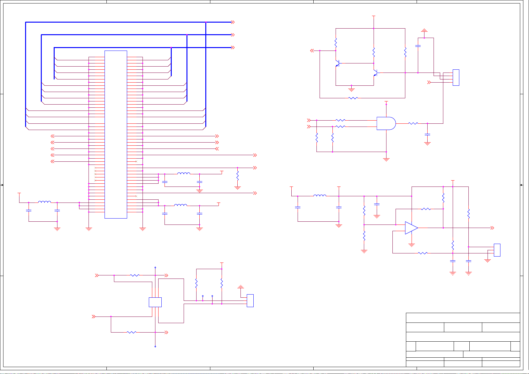
5
4
VOUT_BV[7..0]
3
2
P3P3V
1
LAMOLITZ CIRCUIT
VOUT_GY[7..0]
MHSYNCZ
MVSYNCZ
LAMPLITZ
P3P3V
VOUT_RU[7..0]
R125
10K
RESETZ
PWRGOOD
SYNCVALID
P3P3V
LAMPLITZ
RESETZ
LAMPEN
MMBT2222AWT1
R123
10K
C34
0.047U KC28
L9
120 OHM
D D
1
VOUT_RU7
VOUT_RU5
VOUT_RU3
VOUT_RU1
VOUT_GY7
VOUT_GY5
VOUT_GY3
VOUT_GY1
VOUT_BV7
VOUT_BV5
VOUT_BV3
VOUT_BV1
C C
P12V
B B
CLKIN
VIO20/M_DACT
SDA_DI
SCL_DI
BALLAST_CTRL
L8
80 OHM
0.1U Z
P12V_IN
C29
0.1U Z
3
5
7
9
11
13
15
17
19
21
23
25
27
29
31
33
35
37
39
43
45
47
49
51
53
55
57
59
61
63
65
67
69
71
73
75
77
79
81
83
85
87
89
91
93
95
97
99
20C1001100
1
3
5
7
9
11
13
15
17
19
21
23
25
27
29
31
33
35
37
39
43
45
47
49
51
53
55
57
59
61
63
65
67
69
71
73
75
77
79
81
83
85
87
89
91
93
95
97
99
2
2
J2
4
4
6
6
8
8
10
10
12
12
14
14
16
16
18
18
20
20
22
22
24
24
26
26
28
28
30
30
32
32
34
34
36
36
38
38
40
40
44
44
46
46
48
48
50
50
52
52
54
54
56
56
58
58
60
60
62
62
64
64
66
66
68
68
70
70
72
72
74
74
76
76
78
78
80
80
82
82
84
84
86
86
88
88
90
90
92
92
94
94
96
96
98
98
100
100
VOUT_RU6
VOUT_RU4
VOUT_RU2
VOUT_RU0
VOUT_GY6
VOUT_GY4
VOUT_GY2
VOUT_GY0
VOUT_BV6
VOUT_BV4
VOUT_BV2
VOUT_BV0
P3P3V_IN
P5V_IN
C24
0.1U Z
L7
C26
0.1U Z
L6
80 OHM
80 OHM
C25
0.1U Z
C27
0.1U Z
P5V
INPUT SIGNALS FROM MAIN BOARD
TP50
R119
4.7K
P3P3V
R120
4.7K
TP49
SCL_DTI
SDA_DTI
(IIC From Computer)
J5
3
2
1
20L2021003
3
TP51
R121
R122
NC_R0603
NC_R0603
44556
11223
TP52
6
3
4
SCL_D
SW2
2240138001
SDA_D
(Connector for DLP FALSH DOWNLOAD)
SCL_DI
(IIC From Main CPU)
SDA_DI
A A
5
Q1
R124
R112
R16
1K
32
1
MMBT2222AWT1
R126
NC
1K
1K
R111
10K
3V3_SENSOR
C35
4.7U Z
(1206)
LAMPD
2
R26
10K
R29
6.8K
Q2
10K
32
1
2
2V_REF
R17
1
P3P3V
U11A
14
3
7
74ACT08MTC
LAMPEN CIRCUIT
C36
0.047U K
CWSPPED1 CWSPEED
CWINDEX CIRCUIT
C22
0.047U K
R18
2K
20D0038104
1
2
3
4
J1
3V3_SENSOR
R22
2K
R25
75K
C33
10P J
R24
180
OPDIODE
C30
0.1U Z
CWINDEX
(To DDP1010)
J3
1
2
3
20L2021003
BALLAST_CTRL
R19
47
25
3
+
4
-
LMC7225
LAMPHIGH
R27
510K
1
U4
R28
10K
TURNON
C23
0.047U K
INPUTS, LAMPEN, LAMPLIZ, CWINDEX
Benq Corporation
Project Code
99.J5877.001
Title
Size Document Number R ev.
PCB P/N
<Size>
48.J5802.S01
Tuesday, January 14, 2003
Date: Sheet
Prepared By
ANGEL HU
Model Name
HT720G
DMD BOARD
PCB Rev.
S01
Reviewed By Approved By
ALEX HY TSENG BEN CHEN
OEM/ODM Model Name
99.J5877.R22-C3-304-002
18
1
NA
of
0
Page 81
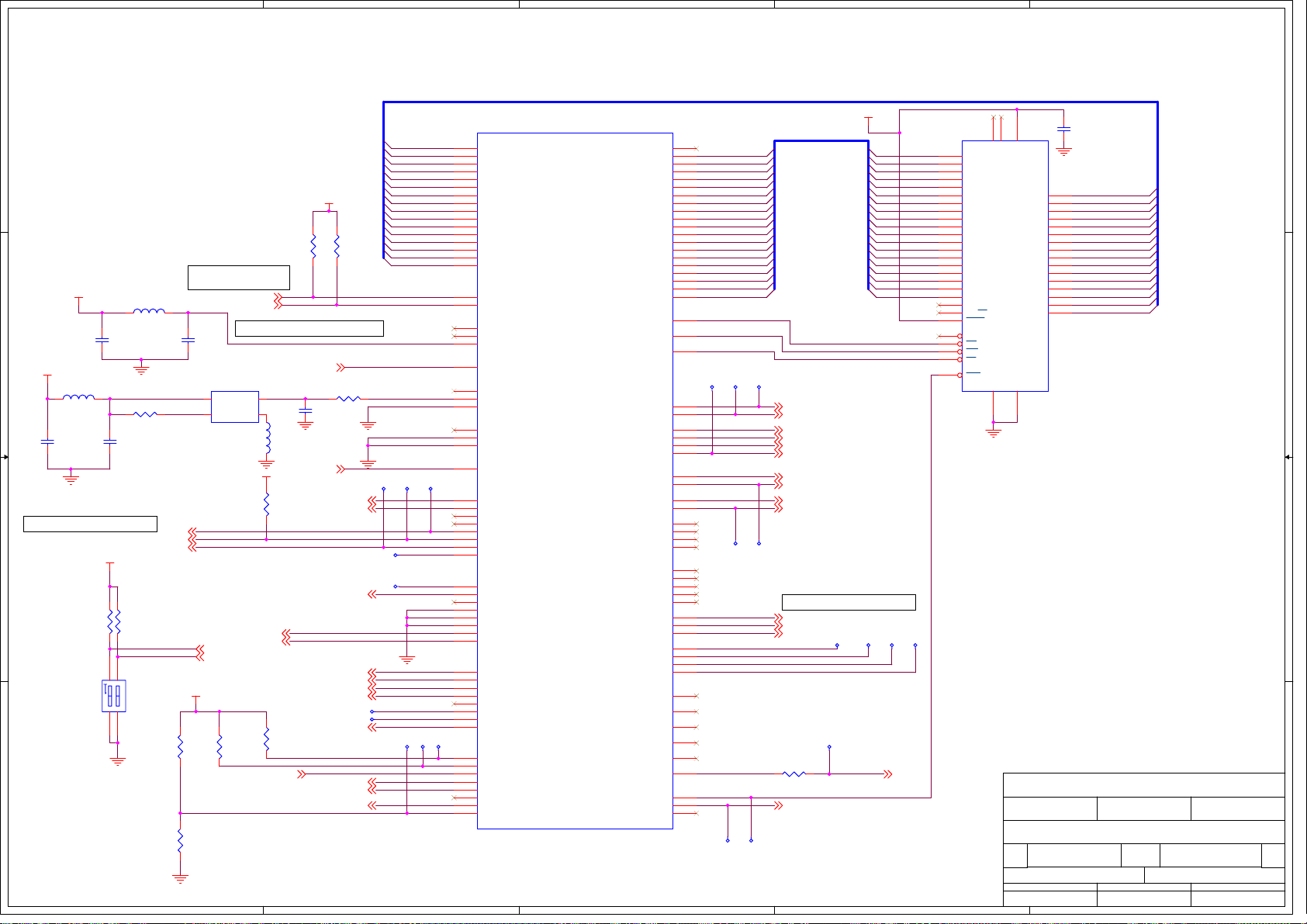
5
4
3
2
1
D D
FLDATA0
FLDATA1
FLDATA2
FLDATA3
FLDATA4
FLDATA5
P5V
R7
10K
R8
10K
FLDATA6
FLDATA7
FLDATA8
FLDATA9
FLDATA10
FLDATA11
FLDATA12
FLDATA13
FLDATA14
FLDATA15
AG26
AH26
AJ26
AF25
AG25
AJ25
AJ24
AF24
AG24
AH24
AF23
AG23
AG22
AJ22
AF20
AJ21
FLDATA0
FLDATA1
FLDATA2
FLDATA3
FLDATA4
FLDATA5
FLDATA6
FLDATA7
FLDATA8
FLDATA9
FLDATA10
FLDATA11
FLDATA12
FLDATA13
FLDATA14
FLDATA15
IIC Bus (open drain)
DDP2P5V
C C
P3P3V
L5
120 OHM
C19
0.1U Z
C17
0.1U Z
C20
0.1U Z
L4
120 OHM
R11
10K
VDDMOSC
MOSCEN
C18
0.1U Z
Pixel Clock (74.25MHz) from Scalar
SERIES CONTROL PORT 0
(To MUSTANG)
DDP3P3V
B B
R13
1.33KF
4
1
A A
R14
1.33KF
3
SW1
6240019001
2
SCPDO
SCPDI
SCPCLK
DDP3P3V
R115
10K
DIO31
R116
NC_R0603
5
SDA_D
SCL_D
Minimize Noise on PLL_VCCA
Master Clock (100MHz)
4
VCC
1
OE
68.00129.0D1
DMDSPARE0
DMDSPARE1
OUT
GND
Y1
100MHZ
DDP3P3V
DMDSPARE0
DMDSPARE1
3
2
L19
220OHM
R12
1K
CLKIN
(To SSI Motor)
R113
10K
R114
10K
CWINDEX
OCLKA
C31
22P J
R10
39.2F
DRCGPDZ
DADSELZ
MTRPWM
MTRRSTZ
MTRSELZ
MTRCLK
MTRDATA
TP2
TP1
DADINTZ
DIO24
IDO25
MTRDMUX
DMDRSTZ
DMDSELZ
MCRYSTALEN
TP29
TP30
PWM0
TP31
PWM1
TP32
TP33
4
MOSC
TP28
ARMTEST1
ARMTEST2
TP26
TP27
AH23
SDA0
AF22
SCL0
AG28
APLLMD1
AF28
APLLMD0
AG29
PLL_VCCA
AF27
COSC
F3
MOSCN
F2
MOSC
G4
MCRYSTALEN
G3
POSCN
G2
POSC
H4
PCRYSTALEN
T26
WCLK
AB28
DIO0
AA26
DIO1
AB27
DIO2
AB26
DIO3
AC28
DIO4
AC27
DIO5
AC26
DIO6
AD28
DIO7
AD27
DIO8
AD29
DIO9
AE28
DIO10
AE29
DIO11/ASICID0
AE27
DIO12/ASICID1
AE26
DIO13/ASICID2
AF29
DIO14
AH3
DIO15
AG4
DIO16
AH4
DIO17
AJ4
DIO18
AF5
DIO19
AG5
DIO20
AH6
DIO21
AF7
DIO22
AG7
DIO23
AB3
DIO24
AB4
DIO25
AC2
DIO26
AC3
DIO27
AC4
DIO28
AD2
DIO29
AD3
DIO30
AD4
DIO31
Micro, Clocks ,SR16 and Flash interface
DDP1010
U2B
FLADDR19
FLADDR18
FLADDR17
FLADDR16
FLADDR15
FLADDR14
FLADDR13
FLADDR12
FLADDR11
FLADDR10
FLADDR09
FLADDR08
FLADDR07
FLADDR06
FLADDR05
FLADDR04
FLADDR03
FLADDR02
FLADDR01
SR16STRB
SR16ADDR3
SR16ADDR2
SR16ADDR1
SR16ADDR0
SR16MODE1
SR16MODE0
SR16SEL1
SR16SEL0
SR16VCCEN
DMDVCCEN
SCP1_CLK
SCP1_DO
PUM_ARSTZ
EXT_ARSTZ
EXT_ARST
DDP1010
FLADDR0
FL_OE
FL_WE
FL_CS
SR16OEZ
DMDBIN3
DMDBIN2
DMDBIN1
DMDBIN0
VCC2EN
VBIASEN
VRSTEN
SCP1_DI
TSTPNT3
TSTPNT2
TSTPNT1
TSTPNT0
OCLKF
OCLKE
OCLKD
OCLKC
OCLKB
OCLKA
3
AH7
FLADDR18
AF8
FLADDR17
AG8
FLADDR16
AF9
FLADDR15
AG9
FLADDR14
AH9
FLADDR13
AG10
FLADDR12
AJ10
FLADDR11
AG13
FLADDR10
AH13
FLADDR9
AJ14
FLADDR8
AF15
FLADDR7
AJ15
FLADDR6
AJ17
FLADDR5
AH17
FLADDR4
AH18
FLADDR3
AG19
FLADDR2
AH20
FLADDR1
AJ20
FLADDR0 FLADDR18
AG20
AH27
AJ27
AF19
TP39
TP40
V2
W3
R4
R1
U1
U2
N2
P1
Y2
Y1
J3
K3
K1
N3
AB1
Y4
AA1
Y3
W4
AF1
AF2
AF3
A21
D19
C20
A20
J2
H3
F1
E1
D1
E3
C1
D2
D3
TP34
TP37
TSTPNT3
TSTPNT2
TSTPNT1
TSTPNT0
OCLKA1
TP35
FLADDR[0..18]
TP41
SR16STROBE
SR16OEZ
SR16ADDR3
SR16ADDR2
SR16ADDR1
SR16ADDR0
SR16MODE1
SR16MODE0
SR16SEL1
SR16SEL0
TP38
SERIES CONTROL PORT 1
SCP_CLK
SCP_DO
SCP_DI
(v-sync, delay CWI, spoketest for debug)
R15
22
PUM_ARSTZ
EXT_ARSTZ
P3P3V
FL_OEZ
FL_WEZ
FL_CSZ
(To DAD1000)
(To DAD1000)
TP45
TP46
TP36
50MHz Clock
(To DAD1000)
TP47
OCLKA
2
FLADDR0
FLADDR1
FLADDR2
FLADDR3
FLADDR4
FLADDR5
FLADDR6
FLADDR7
FLADDR8
FLADDR9
FLADDR10
FLADDR11
FLADDR12
FLADDR13
FLADDR14
FLADDR15
FLADDR16
FLADDR17
TP48
13
10
U3
25
A0
24
A1
23
A2
22
A3
21
A4
20
A5
19
A6
18
A7
8
A8
7
A9
6
A10
5
A11
4
A12
3
A13
2
A14
1
A15
48
A16
17
A17
16
A18
9
NC
15
RY/BY
47
BYTE
14
NC
28
OE
11
WE
26
CE
12
RST
37
NC
NC
VCC
29
D0
31
D1
33
D2
35
D3
38
D4
40
D5
42
D6
44
D7
30
D8
32
D9
34
D10
36
D11
39
D12
41
D13
43
D14
45
D15/A-1
29LV800BB-90EC
VSS
27
FLASH
VSS
AM29LV800BB-120EC
46
7229800219
(Pin 14 shoul d b e d is co nn ected from P3P3V)
DDP1010 Flash, Micro, Clocks, DAD1000 Control
Benq Corporation
Project Code
99.J5877.001
Title
Size Document Number R ev.
PCB P/N
<Size>
48.J5802.S01
Tuesday, January 14, 2003
Date: Sheet
Prepared By
ANGEL HU
FLDATA[0..15]FLDATA[0..15]
C21
0.1U Z
FLDATA0
FLDATA1
FLDATA2
FLDATA3
FLDATA4
FLDATA5
FLDATA6
FLDATA7
FLDATA8
FLDATA9
FLDATA10
FLDATA11
FLDATA12
FLDATA13
FLDATA14
FLDATA15
Model Name
HT720G
DMD BOARD
PCB Rev.
S01
Reviewed By Approved By
ALEX HY TSENG BEN CHEN
1
OEM/ODM Model Name
NA
99.J5877.R22-C3-304-002
of
28
0
Page 82
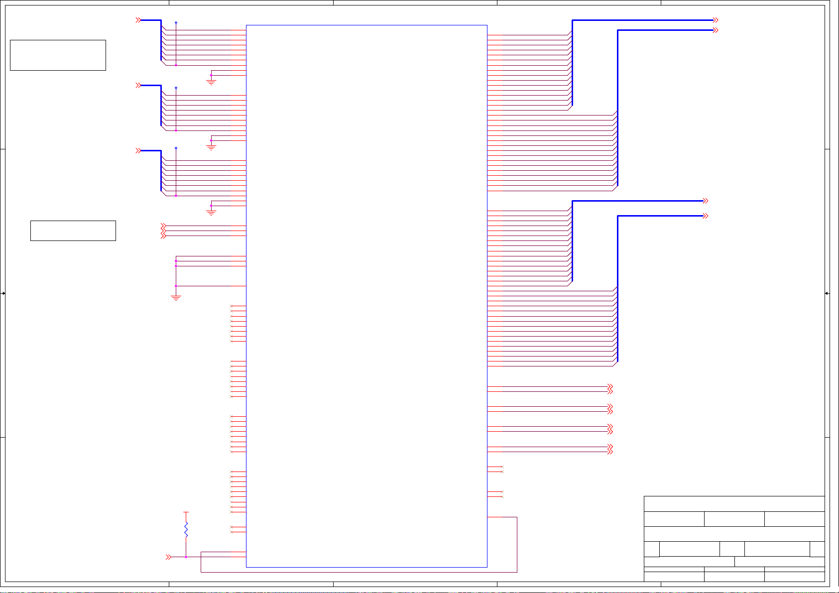
5
VOUT_GY[7..0]
Video Inputs From Scalar
RGB 888 Format (24bits)
D D
C C
B B
A A
Video Syncs From Scalar
VOUT_BV[7..0]
VOUT_RU[7..0]
5
VIO20/M_DACT
MVSYNCZ
MHSYNCZ
SYNCVALID
TP42
TP43
TP44
VOUT_GY7
VOUT_GY6
VOUT_GY5
VOUT_GY4
VOUT_GY3
VOUT_GY2
VOUT_GY1
VOUT_GY0
VOUT_BV7
VOUT_BV6
VOUT_BV5
VOUT_BV4
VOUT_BV3
VOUT_BV2
VOUT_BV1
VOUT_BV0
VOUT_RU7
VOUT_RU6
VOUT_RU5
VOUT_RU4
VOUT_RU3
VOUT_RU2
VOUT_RU1
VOUT_RU0
DDP3P3V
R70
(NC)
FSD16
M28
M27
M26
W29
W27
K28
K29
K27
K26
H29
H28
N29
N28
N27
N26
R26
R27
R28
R29
P29
P28
P27
P26
U26
U28
U27
V26
V28
E28
E29
E27
E26
D29
B27
A27
D24
C24
B24
D23
C23
B23
D22
C22
C26
B26
A26
D25
C25
A25
B25
A24
H27
H26
G28
G27
G26
C28
L26
J29
J28
J27
L28
L29
L27
T28
T29
F29
F28
F27
F26
J26
Y28
Y29
T27
4
A9
A8
A7
A6
A5
A4
A3
A2
A1
A0
B9
B8
B7
B6
B5
B4
B3
B2
B1
B0
C9
C8
C7
C6
C5
C4
C3
C2
C1
C0
MACT
MVSYNCZ
MHSYNCZ
SACT
SVSYNCZ
SHSYNCZ
OSDACT
RMG7
RMG6
RMG5
RMG4
RMG3
RMG2
RMG1
RMG0
RMB7
RMB6
RMB5
RMB4
RMB3
RMB2
RMB1
RMB0
RMR7
RMR6
RMR5
RMR4
RMR3
RMR2
RMR1
RMR0
RMA7
RMA6
RMA5
RMA4
RMA3
RMA2
RMA1
RMA0
RMACT
RMVSYNCZ
RMHSYNCZ
FILEDSYNC
SYNCVALID2
4
U2C D DP1010
3
H1
DDAP15
J1
DDAP14
K2
DDAP13
L1
DDAP12
L2
DDAP11
M2
DDAP10
N1
DDAP9
P3
DDAP8
T3
DDAP7
U3
DDAP6
V3
DDAP5
V4
DDAP4
AA2
DDAP3
AB2
DDAP2
AD1
DDAP1
AE3
DDAP0
K4
DDAN15
L4
DDAN14
L3
DDAN13
M4
DDAN12
M3
DDAN11
N4
DDAN10
P4
DDAN9
P2
DDAN8
T4
DDAN7
U4
DDAN6
W2
DDAN5
W1
DDAN4
AA3
DDAN3
AA4
DDAN2
AE2
DDAN1
AE4
DDAN0
AH22
DDBP15
AH21
DDBP14
AF18
DDBP13
AG18
DDBP12
AG17
DDBP11
AG16
DDBP10
AJ16
DDBP9
AG15
DDBP8
AH12
DDBP7
AH11
DDBP6
AJ11
DDBP5
AH10
DDBP4
AJ9
DDBP3
AH8
DDBP2
AF6
DDBP1
AJ5
DDBP0
AF21
DDBN15
AG21
DDBN14
AJ19
DDBN13
AH19
DDBN12
AF17
DDBN11
AF16
DDBN10
AH16
DDBN9
AH15
DDBN8
AF13
DDBN7
AG12
DDBN6
AF12
DDBN5
AG11
DDBN4
AF11
DDBN3
AJ8
DDBN2
AG6
DDBN1
AH5
DDBN0
T1
DCKAP
T2
DCKAN
R3
SCAP
R2
SCAN
AJ13
DCLKBP
AF14
DCLKBN
AG14
SCBP
AH14
SCBN
AA27
RMHSOZ
AA28
RMVSOZ
Y27
HSYNCOZ
W26
VSYNCOZ
AA29
FSD16
3
DDAP15
DDAP14
DDAP13
DDAP12
DDAP11
DDAP10
DDAP9
DDAP8
DDAP7
DDAP6
DDAP5
DDAP4
DDAP3
DDAP2
DDAP1
DDAP0
DDAN15
DDAN14
DDAN13
DDAN12
DDAN11
DDAN10
DDAN9
DDAN8
DDAN7
DDAN6
DDAN5
DDAN4
DDAN3
DDAN2
DDAN1
DDAN0
DDBP15
DDBP14
DDBP13
DDBP12
DDBP11
DDBP10
DDBP9
DDBP8
DDBP7
DDBP6
DDBP5
DDBP4
DDBP3
DDBP2
DDBP1
DDBP0
DDBN15
DDBN14
DDBN13
DDBN12
DDBN11
DDBN10
DDBN9
DDBN8
DDBN7
DDBN6
DDBN5
DDBN4
DDBN3
DDBN2
DDBN1
DDBN0
2
1
DDAP[15..0]
DDAN[15..0]
LVDS Differential DataBus DDA
(To Mustang DMD)
LVDS Differential DataBus DDB
(To Mustang DMD)
DDBP[15..0]
DDBN[15..0]
DCLKAP
LVDS Differential DCLKA
DCLKAN
LVDS Differential Series Control Bus A
SCTRLAP
SCTRLAN
LVDS Differential DCLKB
DCLKBP
DCLKBN
LVDS Differential Series Control Bus B
SCTRLBP
SCTRLBN
DDP1010 Video Input and DMD Output
Benq Corporation
Project Code
99.J5877.001
Title
Size Document Number R ev.
PCB P/N
<Size>
48.J5802.S01
Tuesday, January 14, 2003
Date: Sheet
Prepared By
2
ANGEL HU
Model Name
HT720G
DMD BOARD
PCB Rev.
S01
Reviewed By Approved By
ALEX HY TSENG BEN CHEN
OEM/ODM Model Name
99.J5877.R22-C3-304-002
38
1
NA
0
of
Page 83
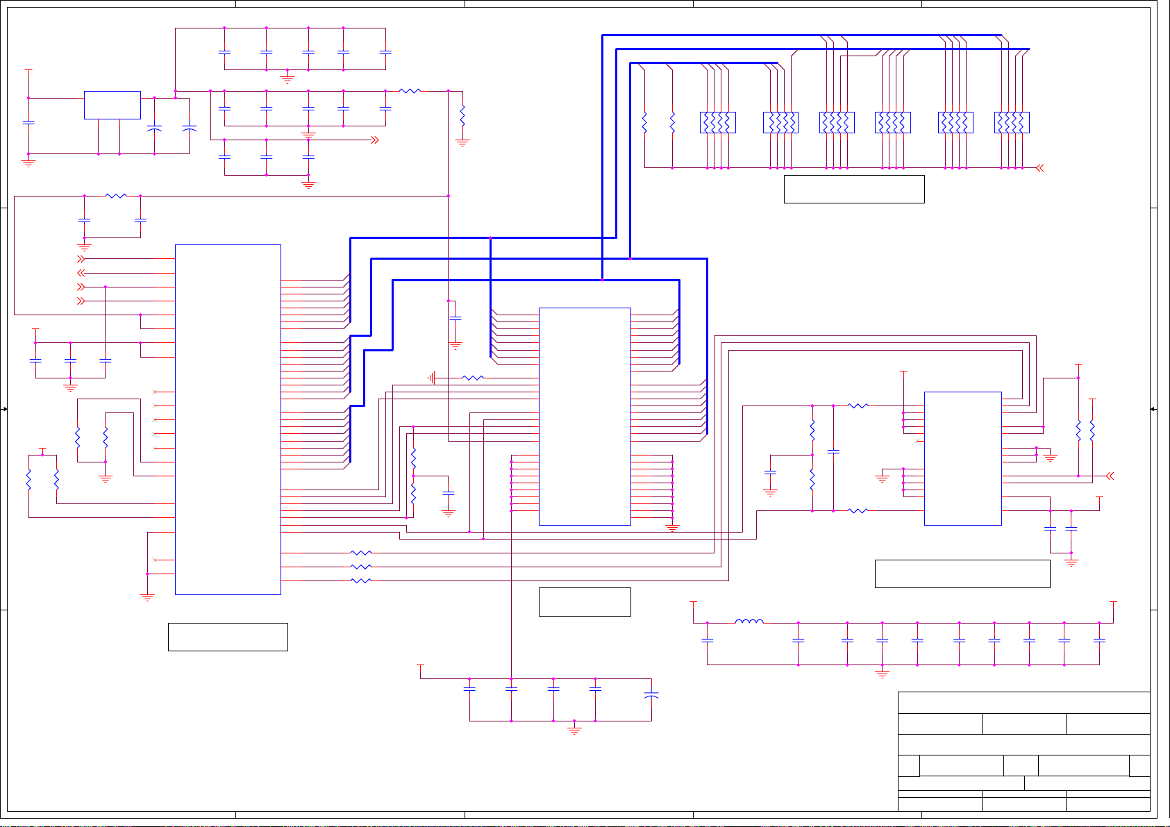
5
4
3
2
1
VTERM (1.8V) Bulk Decoupling Caps
C209
C208
C207
DDP3P3V
D D
C223
4.7U Z
(1206)
VREF_ASIC
MIC39100-1.8BS
1
IN
U10
OUT
GND12GND2
4
R108
110F
3
12
12
C231
+
+
100U
6.3V
C230
100U
6.3V
0.1U Z
C218
0.1U Z
C226
0.1U Z
0.1U Z
C219
0.1U Z
C227
0.1U Z
0.1U Z
C220
0.1U Z
C228
0.1U Z
0.1U Z
0.1U Z
C210
C221
C211
0.1U Z
C222
0.1U Z
VTERM
VREF_RDRAM
R109
3.4KF
R110
11.8KF
DQA3
R6
39.2F
DQA8
R9
39.2F
RN6
DQA4
876
123
DQA0
DQA7
DQA6
5
4
RQ5
DQA1
DQA2
DQA5
876
5
39
39
123
4
RN5
RN4
DQB5
DQB6
876
123
RQ0
DQB2
5
4
RQ4
RQ6
RQ1
876
RN3
123
5
4
39
DQB8
DQB7
DQB3
DQB4
876
5
123
39
4
39
RN2
Termination Components
RN1
DQB1
876
123
RQ2
DQB0
RQ3
5
4
39
VTERM
1.8V
RQ7
C213
0.1U Z
C212
0.1U Z
Rambus, JTAG and Customer Input
TRSTZ
TCK
5
V27
Y26
AG2
C2
A11
B8
B9
D12
E4
C29
J4
D27
B3
AG1
C4
A3
D28
AJ3
W28
E2
LAMPLITZ
LAMPEN
PWRGOOD
RESETZ
C C
VREF_ASIC
DDP2P5V
C195
68P J
R117
1K
C196
0.1U Z
R118
1K
ICEOENZ
ICTSENZ
C194
0.1U Z
JTAG is inactive for normal operation
DDP3P3V
R102
R101
10K
10K
B B
A A
U2A
DDP1010
LAMPSTAT
LAMPCTRL
PWRGOOD
STARTZ
RD_VREF1
RD_VREF0
RD_AVDD0
RD_AVDD1
TDO2
TMS2
TDO1
TMS1
TDI
TRSTZ/IBMT_LT
TCK
ICEOENZ
ICTSENZ
IBMT_RI
POSTST
LSSDEN
RQ7
RQ6
RQ5
RQ4
RQ3
RQ2
RQ1
RQ0
DQA8
DQA7
DQA6
DQA5
DQA4
DQA3
DQA2
DQA1
DQA0
DQB8
DQB7
DQB6
DQB5
DQB4
DQB3
DQB2
DQB1
DQB0
RD_SCK
RD_CMD
RD_SIO
RD_CFM
RD_CFMN
RD_CTM
RD_CTMN
PCLKM
SCLKN
REFCLK
RDRAM Memory Control
B11
C12
C13
B13
D14
C14
A15
B15
A4
D5
B5
A6
C6
B6
C7
B7
D8
C19
A19
B19
C18
C17
B17
D16
C16
A16
B22
A22
D21
D10
C9
C10
D11
C21
D20
B21
RQ7
RQ6
RQ5
RQ4
RQ3
RQ2
RQ1
RQ0
DQA8
DQA7
DQA6
DQA5
DQA4
DQA3
DQA2
DQA1
DQA0
DQB8
DQB7
DQB6
DQB5
DQB4
DQB3
DQB2
DQB1
DQB0
SCK
CMD
SIO
CFM
CFMN
CTM
CTMN
PCLKM1
SCLKN1
REFCLK1
R105
R106
R107
RQ[7..0]
4
DQA[0..8]
22
22
22
DQB[0..8]
DDP2P5V
R104
39.2F
R103
39.2F
CLKFM
RamBus Address Channel
RamBus Data Channel A
RamBus Data Channel B
RQ0
RQ1
RQ2
RQ3
RQ4
RQ5
RQ6
RQ7
SIO1
SIO
CMD
SCK
CTM
CTMN
CFM
CFMN
G1
F2
F6
F7
F1
E7
E6
E2
J3
J5
A5
A3
E1
D1
C7
D7
D2
A2
J2
D6
B5
C3
E5
F3
G5
H5
C225
0.1U Z
R95
1K
C201
0.1U Z
RDRAM VDD (2.5V) DECOUPING CAPS
C202
C203
0.1U Z
0.1U Z
RQ0
RQ1
RQ2
RQ3
RQ4
RQ5
RQ6
RQ7
SIO1
SIO0
CMD
SCK
CTM
CTMN
CFM
CFMN
VREF
VCMOS
VCMOS
VDDA
P2P5V
P2P5V
P2P5V
P2P5V
P2P5V
P2P5V
K4R271669DU8
PCLKM
SCLKN
REFCLK
RDRAM
C204
0.1U Z
3
DQB7
DQB6
DQB5
DQB4
DQB3
DQB2
DQB1
DQB0
DQA0
DQA1
DQA2
DQA3
DQA4
DQA5
DQA6
DQA7
GNDA
GND
GND
GND
GND
GND
GND
GND
GND
GND
C205
0.1U Z
NC1
NC2
DQB8
J1
DQB7
J7
DQB6
H2
DQB5
H6
DQB4
H7
DQB3
H1
DQB2
G2
DQB1
G6
DQB0
G7
DQA0
C1
DQA1
C2
DQA2
C6
DQA3
B1
DQA4
B7
DQA5
B6
DQA6
B2
DQA7
A7
DQA8
A1
D5
A6
B3
C5
D3
E3
F5
G3
H3
J6
C198
0.1U Z
CTM
CLKTM
CTMN
R98
56.2F
R99
56.2F
R94
110F
C197
4.7P C
R97
110F
CTM1_M
CTMN1_M
VDRCG
U9
CDCR83
2
REFCLK
20
CLK
3
VDD
9
VDD
16
VDD
22
VDD
19
NC
4
GND
5
GND
8
GND
17
GND
21
GND
18
CLKB
SYNCLKN
PCLKM
MULT0
MULT1
PWRDNB
STOPB
VDDIR
VDDIPD
7
6
15
14
24
S0
23
S1
13
S2
12
STOPZ
11
1
10
C199
0.1U Z
R96
1K
VDRCG
C200
0.1U Z
DDP2P5V
DDP2P5V
R100
1K
DRCGPDZ
Direct Rambus Clock Generator (DRCG)
L18
120 OHM
C184
0.1U Z
12
C229
+
150U
6.3V
C185
4.7U Z
(1206)
2
CDCR83 (DRCG) 3.3V Decoupling Caps
C188
C186
0.1U Z
C187
0.1U Z
68P J
Benq Corporation
Project Code
99.J5877.001
Title
Size Document Number R ev.
PCB P/N
<Size>
48.J5802.S01
Tuesday, January 14, 2003
Date: Sheet
Prepared By
ANGEL HU
C190
C189
68P J
Model Name
DMD BOARD
C191
0.1U Z
68P J
HT720G
PCB Rev.
99.J5877.R22-C3-304-002
S01
Reviewed By Approved By
ALEX HY TSENG BEN CHEN
1
VDRCGP3P3V
C192
C193
0.1U Z
68P J
OEM/ODM Model Name
NA
of
48
0
Page 84
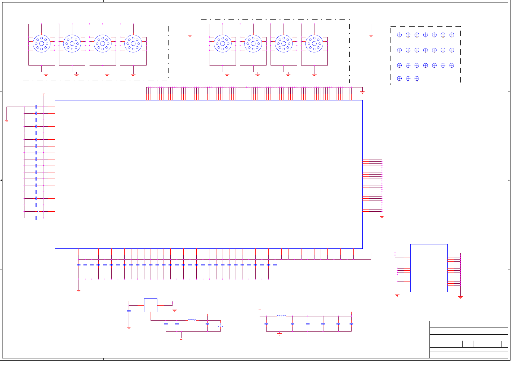
5
4
3
2
1
J25
GNDJ5GND
M29
GNDM1GND
N25
GNDN5GND
Screw Holes
5
4
3
2
H5
HOLE-V8
U25
U29
GNDU5GND
GND
GNDV1GND
Optical Points
MARK2
MARK4
OP
MARK14
OP
MARK15
OP
MARK5
OP
MARK17
OP
MARK16
OP
MARK6
OP
MARK18
OP
MARK19
OP
MARK7
OP
MARK20
OP
MARK21
OP
MARK3
MARK1
OP
OP
1
9
8
7
6
V29
AA5
AA25
AB29
AC1
AC29
AD26
GND
GND
GND
GND
GND
1
5
9
4
8
3
7
2
6
H6
HOLE-V8
AE1
M14
M15
M16
M17
M18
N12
N13
N14
M13
M12
GND
GND
GND
GND
GND
GND
GND
GND
GND
GND
GND
1
5
9
4
8
3
7
2
6
H7
HOLE-V8
N15
N16
N17
N18
P12
P13
P14
P15
P16
P17
P18
R12
R13
R14
GND
GND
GND
GND
GND
GND
GND
GND
GND
GND
GND
GND
GND
GND
1
5
9
4
8
3
7
2
6
H8
HOLE-V8
R15
R16
R17
R18
T12
T13
T14
T15
T16
T17
T18
U12
U13
U14
U15
U16
U17
U18
V12
V13
V14
GND
GND
GND
GND
GND
GND
GND
GND
GND
GND
GND
GND
GND
GND
GND
GND
GND
GND
GND
GND
GND
GND
U2D
V15
V16
V17
V18
DDP1010
GND
GND
GND
GND
AJ29
GND
AJ28
GND
AJ23
GND
AJ18
GND
AJ12
GND
AJ7
GND
AJ6
GND
AJ2
GND
AJ1
GND
AH29
GND
AH28
GND
AH25
GND
AH2
GND
AH1
GND
AG27
GND
AG3
GND
AF26
GND
AF10
GND
AF4
GND
AE25
GND
AE21
GND
AE17
GND
AE13
GND
AE9
GND
AE5
GND
OP
MARK9
OP
MARK8
OP
MARK22
OP
MARK11
OP
MARK10
OP
MARK23
OP
MARK12
OP
MARK13
OP
MARK24
OP
Screw Holes
1
5
9
4
8
3
D D
C C
B B
2
H1
HOLE-V8
C119 0.1U Z
C120 0.1U Z
C121 0.1U Z
C122 0.1U Z
C123 0.1U Z
C124 0.1U Z
C125 0.1U Z
C126 0.1U Z
C127 0.1U Z
C128 0.1U Z
C129 0.1U Z
C130 0.1U Z
C131 0.1U Z
C132 0.1U Z
C133 0.1U Z
C134 0.1U Z
C135 0.1U Z
C136 0.1U Z
DDP3P3V
7
6
AE20
AE19
AE18
AE12
AE11
AE10
Y5
W5
V5
M5
L5
K5
Y25
W25
V25
M25
L25
K25
VCC33
VCC33
VCC33
VCC33
VCC33
VCC33
VCC33
VCC33
VCC33
VCC33
VCC33
VCC33
VCC33
VCC33
VCC33
VCC33
VCC33
VCC33
5
4
3
2
H2
HOLE-V8
1
9
8
7
6
5
4
3
2
H3
HOLE-V8
1
9
8
7
6
5
4
3
2
H4
HOLE-V8
1
9
8
7
6
A12
A18
A23
A28
A29
B28
B29
C27
D26
E13
E17
E21
E25
G29
GNDA1GNDA2GNDA7GND
GND
GND
GND
GND
GNDB1GNDB2GND
GND
GNDC3GND
GNDD4GND
GNDE5GNDE9GND
GND
GND
GND
GNDF4GNDG1GND
VCC25
VCC25
VCC25
VCC25
VCC25
VCC25
VCC25
VCC25
VCC25
F25
H25
G25
C137
C139
C138
0.1U
0.1U
0.1U
A A
T25
P25
R25
AB25
AC25
AD25
C140
0.1U
C143
C142
C141
0.1U
0.1U
C145
C144
0.1U
0.1U
0.1U
P3P3V
4.7U Z
(1206)
C148
C147
C146
0.1U
0.1U
0.1U
U7
MIC39100
1
C180
3
C151
C150
C149
0.1U
0.1U
0.1U
4
GND
GND2IN
OUT
P2P5V_IN
C181
4.7U Z
(1206)
2.5V Regulator and Decoupling Caps
VCC25F5VCC25G5VCC25H5VCC25P5VCC25R5VCC25T5VCC25H2VCC25
5
4
VCC25
VCC25
VCC25
VCC25
VCC25
VCC25
VCC25
VCC25
VCC25
VCC25
VCC25
VCC25E6VCC25E7VCC25E8VCC25
AB5
C153
C152
0.1U
0.1U
C182
0.1U Z
AC5
C154
0.1U
L17
80 OHM
AE6
AE7
C156
0.1U
C157
0.1U
DDP2P5V
C183
0.1U Z
AE8
AE14
AE15
AE16
AE22
AE23
C159
C158
0.1U
C161
C160
0.1U
0.1U
0.1U
12
+
C236
150U
6.3V
AE24
C164
C163
C162
0.1U
0.1U
C166
C165
0.1U
0.1U
0.1U
P3P3V
C115
0.1U Z
AD5
C155
0.1U
C167
0.1U
VCC25
VCC25
VCC25
VCC25
VCC25
E14
E15
E16
E22
E23
E24
E10
L15
80 OHM
C232
C116
4.7U Z
0.1U Z
(1206) (1206) (1 206) (1206) (1206)
VCC25
C233
4.7U Z
VCC25
E11
VCC25
E12
VCC25
E18
C234
4.7U Z
VCC25
E19
E20
DDP3P3V
VCC25
C235
4.7U Z
DDP2P5V
DDP3P3V Decoupling Caps
3
2
DDP2P5V
B20
D15
B18
A14
D13
A10
B4
C5
C8
U2E
RD_VDD5
RD_VDD3
RD_VDD0
RD_RGND10
RD_RGND7
RD_RGND6
RD_RGND4
RD_RGND0
RD_RGNDC
DDP1010
D18
RD_RSGND17
D17
RD_RSGND16
A17
RD_RSGND15
B16
RD_RSGND14
C15
RD_RSGND13
B14
RD_RSGND12
A13
RD_RSGND11
B12
RD_RSGND10
C11
RD_RSGND9
B10
RD_RSGND8
A9
RD_RSGND7
A8
RD_RSGND6
D9
RD_RSGND5
D7
RD_RSGND3
D6
RD_RSGND2
A5
RD_RSGND1
Benq Corporation
Project Code
99.J5877.001
Title
Size Document Number Rev.
PCB P/N
<Size>
Tuesday, January 14, 2003
Date: Sheet
Prepared By
ANGEL HU
Model Name
DMD BOARD
48.J5802.S01
1
OEM/ODM Model Name
HT720G
PCB Rev.
99.J5877.R22-C3-304-002
S01
Reviewed By Approved By
ALEX HY TSENG BEN CHEN
NA
58
of
0
Page 85
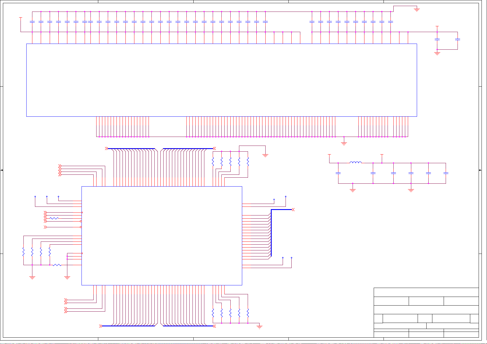
5
4
3
2
1
VCC
D D
C63
0.1U
A3
VCC
C64
0.1U
A11
VCC
C65
0.1U
A21
VCC
C66
0.1U
A13
VCC
C67
0.1U
A33
VCC
C68
0.1U
A27
VCC
C69
0.1U
A35
VCC
C70
0.1U
B38
VCC
C71
C72
0.1U
0.1U
VCCC1VCCD2VCC
C73
0.1U
E1
C74
0.1U
F40
VCC
C75
0.1U
F4
VCC
C76
0.1U
VCCJ3VCC
C77
0.1U
J39
C78
0.1U
C80
C79
0.1U
0.1U
M40
VCCK2VCCL1VCC
C82
C81
0.1U
0.1U
VCCP4VCCR3VCC
C84
C85
C83
0.1U
0.1U
0.1U
R39
VCCT2VCCU1VCCV2VCCW3VCC
C86
0.1U
C87
0.1U
C88
0.1U
W39
C90
C89
0.1U
0.1U
Y14
VCCY4VCC
C96
C95
0.1U
0.1U
Y22
Y28
Y34
Y36
VCC
VCC
VCC
VCC
VCC2F2VCC2G1VCC2H2VCC2
C97
0.1U
C98
0.1U
H38
C100
C99
C101
0.1U
0.1U
0.1U
H40
VCC2
VCC2J1VCC2M2VCC2N1VCC2
C102
0.1U
C103
0.1U
N37
C104
0.1U
N39
VCC2
R1
VCC2P2VCC2
VCC2
C113
1U Z
C114
1U Z
U6B
MUSTANG
GNDA5GND
GND
GNDB2GNDB4GND
GND
GND
GND
GND
GND
GND
GNDC3GNDC7GND
GND
GND
GND
GND
DDAP2
C5
B18
B20
B26
B32
C13
C15
C17
C19
DDAP10
DDAP11
DDAP12
DDAP13
DDAP14
DDAP3
DDAP4
DDAP5
DDAP6
DDAP7
DDAP8
DDAP9
B24
B28
B30
D38
D24
C27
C29
DDAP15
DDAN0
DDAN1
DDAN2
DDAN3
E35
E37
G35
G37
H36
B22
A25
C21
C23
K40
K36
A15
A37
B12
B14
B16
C C
DDAP[15..0]
SCTRLAN
SCTRLAP
DCLKAN
DCLKAP
B34
DDAP0
DDAP1
A23
D22
D34
D36
B36
GND
GND
GND
GND
GND
GNDD4GND
GND
GND
GND
GND
GND
GNDE3GNDE5GNDE7GNDF6GNDF8GND
C25
C31
C35
C37
C39
D10
D16
D18
D20
D26
D32
DDAN[15..0]
R52
DDAN14
DDAN15
K38
K34
RV_A0
C11
RV_A1
10K
D14
RV_A2
B10
RV_A3
A17
DDAN10
DDAN11
DDAN12
D30
DDAN13
DDAN8
DDAN9
E39
G39
G33
H34
D40
E33
DDAN4
DDAN5
DDAN6
DDAN7
A29
A31
D28
R53
10K
A19
RV_A4
R54
10K
GND
GND
F34
F36
F38
R55
10K
GNDG3GNDG5GNDG7GNDH4GNDH6GNDH8GNDJ5GNDJ7GND
J33
R56
10K
GND
GND
J35
J37
GNDK6GNDK8GNDL7GNDM8GND
M34
M36
GND
M38
GND
GNDP8GNDR5GNDR7GND
R33
GND
R35
GND
GNDT4GNDT6GNDT8GNDU3GNDU9GND
GND
GND
R37
U19
U25
U31
P3P3V VCC
C111
0.1U Z
L14
120 OHM
GNDV4GNDV8GND
V14
V20
GND
V26
GND
V32
GND
V36
GND
GND
V38
C112
0.1U Z
GND
GND
GNDW5GND
V40
W15
W21
GND
W33
W27
C107
2.2U Z
GND
GND
GNDY6GND
Y38
Y16
C108
2.2U Z
C109
2.2U Z
C110
2.2U Z
TP6
TP7
TP8
TPM0
U13
TPM1
Y10
TPM2
W11
SCPDOM
EVCC0
EVCC1
EVCC2
EVCC3
0
SCRLR
V34
C33
B6
D6
B8
D8
C9
W9
A7
W7
V6
U7
A9
R58
0
SCPCLK
SCPDO
SCPDI
DMDSELZ
DMDRSTZ
R59
0
R60
R57
33
R61
0
0
R62
B B
DCLK_AP
TP0
TP1
TP2
SCPCK
SCPDI
SCPDO
SCPEN
DMD_RESETB
EVCC
EVCC
EVCC
EVCC
FUSE_CLK
FUSE_DATA
PROG_FUSE_EN
SCR_CLR
DCLK_AN
SCTRL_AP
D_AP0
SCTRL_AN
D_AP2
D_AP1
D_AP4
D_AP3
D_AP5
D_AP6
D_AP8
D_AP7
D_AP9
D_AP10
D_AP11
MUSTANG
D_AP12
D_AP13
U6A
D_AP14
D_AP15
D_AN0
D_AN1
D_AN2
D_AN3
D_AN4
D_AN5
D_AN6
D_AN7
D_AN8
D_AN9
D_AN10
D_AN11
D_AN12
D_AN13
D_AN14
D_AN15
RSV_A0
RSV_A1
RSV_A2
RSV_A3
RSV_A4
READOUTA0
READOUTA1
READOUTB0
READOUTB1
MBRST00
MBRST01
MBRST02
MBRST03
MBRST04
MBRST05
MBRST06
MBRST07
MBRST08
MBRST09
MBRST10
MBRST11
MBRST12
MBRST13
MBRST14
MBRST15
V12
L5
U5
N3
Y12
U15
P6
N5
U17
W13
W17
V16
N7
M4
W19
V18
M6
L3
D12
K4
READOUTA0
READOUTA1
MBRST0
MBRST1
MBRST2
MBRST3
MBRST4
MBRST5
MBRST6
MBRST7
MBRST8
MBRST9
MBRST10
MBRST11
MBRST12
MBRST13
MBRST14
MBRST15
READOUTB0
READOUTB1
TP10
TP11
TP9
MBRST[15..0]
TP12
MUSTANG (HD2) DMD
D_BP0
D_BP2
D_BP4
D_BP6
D_BP8
D_BP10
D_BP12
D_BP14
D_BN0
D_BN2
D_BN4
D_BN6
D_BN8
D_BN10
D_BN12
D_BP1
D_BP3
D_BP5
D_BP7
D_BP9
D_BP11
D_BP13
D_BP15
D_BN1
D_BN3
D_BN5
SCTRL_BN
SCTRL_BP
DCLK_BN
DCLK_BP
L39
L35
T38
U23
DDBP4
T36
Y30
V28
DDBP5
DDBP6
W31
DDBP7
P38
V30
DDBP8
U37
DDBP9
P36
DDBP10
DDBP11
4
N35
DDBP12
DDBP13
W23
DDBP14
DDBP15
DDBN0
V22
DDBN1
Y24
U21
U35
U33
W37
A A
DCLKBP
DCLKBN
SCTRLBP
SCTRLBN
5
W35
DDBP[15..0]
DDBP0
DDBP1
DDBP2
W25
DDBP3
D_BN7
Y26
Y32
V24
U39
U27
U29
W29
DDBN2
DDBN3
DDBN4
DDBN5
DDBN6
DDBN7
DDBN8
D_BN9
T40
T34
DDBN10
DDBN9
D_BN11
P40
P34
N33
DDBN11
DDBN12
DDBN13
D_BN14
D_BN13
L37
L33
DDBN14
DDBN15
D_BN15
RSV_B0
RSV_B1
V10
U11
RVB0
RVB1
RVB2
R63
10K
DDBN[15..0]
RSV_B2Y8RSV_B3
RSV_B4
Y18
Y20
R64
10K
RVB4
RVB3
R65
10K
Benq Corporation
Project Code
99.J5877.001
R66
R67
10K
10K
3
2
Title
Size Document Number R ev.
PCB P/N
<Size>
48.J5802.S01
Tuesday, January 14, 2003
Date: Sheet
Prepared By
ANGEL HU
Model Name
HT720G
DMD BOARD
PCB Rev.
S01
Reviewed By Approved By
ALEX HY TSENG BEN CHEN
OEM/ODM Model Name
99.J5877.R22-C3-304-002
68
1
NA
0
of
Page 86
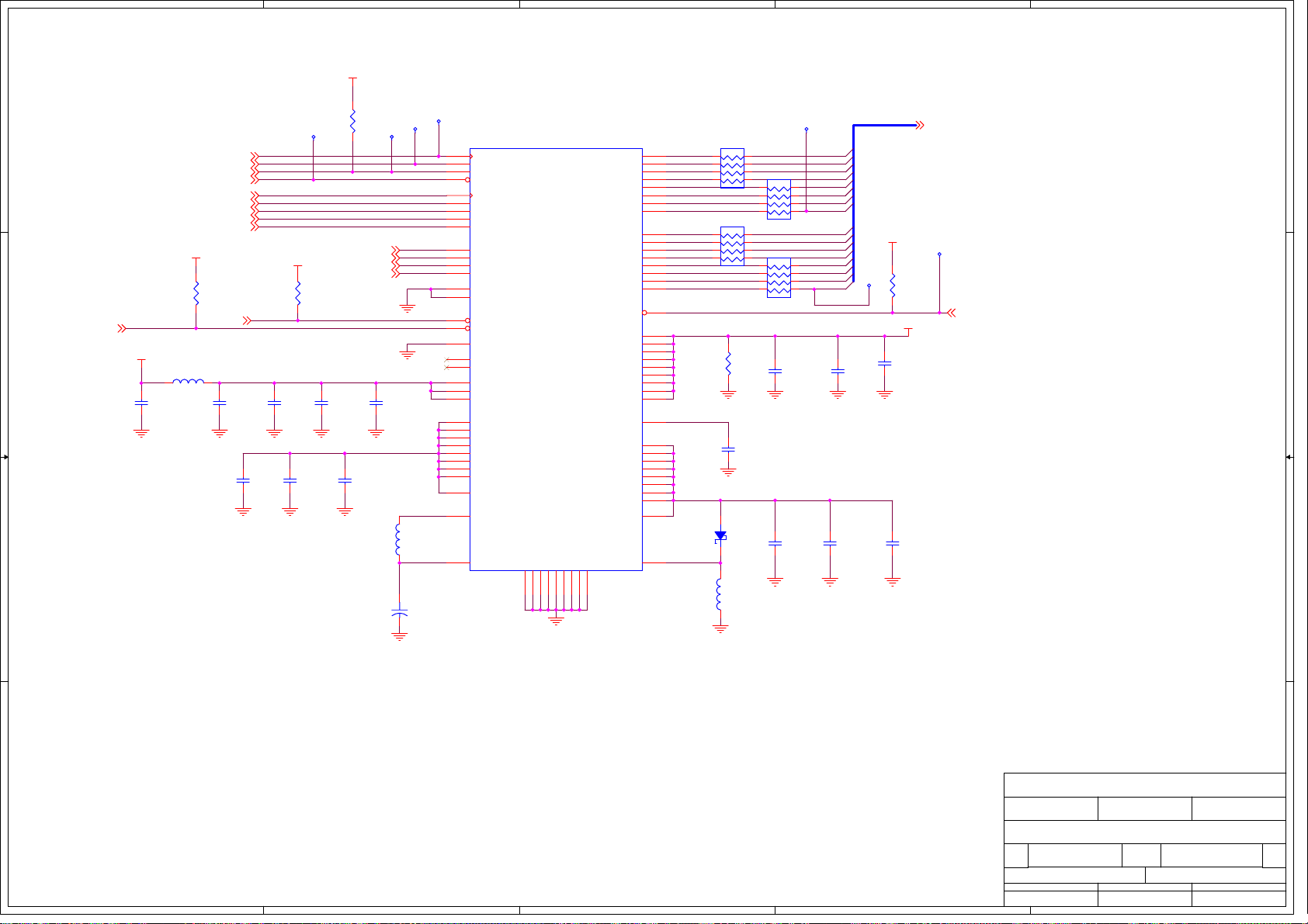
5
P3P3V
4
3
2
1
C8
TP14
VBIAS_SWL
L2
22UH
VBIAS_LHI
12
C16
+
10U
16V
TP13
56
57
42
58
15
2
3
4
5
16
17
18
19
45
44
59
6
54
52
51
50
48
11
80
71
70
61
40
31
30
21
9
8
10
U1
SCP_CLK
SCPDI
SCPDO
SCPENZ
STORBE
MODE1
MODE0
SEL1
SEL0
A3
A2
A1
A0
DAD1000
DEV_ID1
DEV_ID0
RESETZ
OEZ
VCC
V12_SWL1
V12_SWL0
V12_3
V12_2
V12_1
VBIAS_RAIL7
VBIAS_RAIL6
VBIAS_RAIL5
VBIAS_RAIL4
VBIAS_RAIL3
VBIAS_RAIL2
VBIAS_RAIL1
VBIAS_RAIL0
VBIAS
VBIAS_SWL
VBIAS_LHI
GND1GND7GND14GND20GND41GND46GND53GND55GND
60
OUT15
OUT14
OUT13
OUT12
OUT11
OUT10
OUT09
OUT08
OUT7
OUT6
OUT5
OUT4
OUT3
OUT2
OUT1
OUT0
IRQZ
VOFF_RAIL7
VOFF_RAIL6
VOFF_RAIL5
VOFF_RAIL4
VOFF_RAIL3
VOFF_RAIL2
VOFF_RAIL1
VOFF_RAIL0
VOFF
V5REG
VRST_RAIL7
VRST_RAIL6
VRST_RAIL5
VRST_RAIL4
VRST_RAIL3
VRST_RAIL2
VRST_RAIL1
VRST_RAIL0
VRST
VRST_SWL
79
77
74
72
69
67
64
62
39
37
34
32
29
27
24
22
43
78
73
68
63
38
33
28
23
49
47
76
75
66
65
36
35
26
25
13
12
RST15
RST14
RST13
RST12
RST11
RST10
RST9
RST8
RST7
RST6
RST5
RST4
RST3
RST2
RST1
RST0
V5REG
MBR0540T1
VRST_SWL
RP3
5
6
7
8
5
6
7
8
RP1
TP18
10
4
3
2
1
5
6
7
8
RP2
10
4
3
2
1
5
6
7
8
RP4
R5
10K
C9
--> (1U--> 0.22U) for more working margin
0.22U M
(0805)
12
D1
L3
22UH
10
10
C2
0.1U Z
C15
4.7U Z
(50V)
MBRST15
MBRST14
MBRST13
MBRST12
MBRST11
4
MBRST10
3
MBRST9
2
MBRST8
1
MBRST7
MBRST6
MBRST5
MBRST4
MBRST3
4
MBRST2
3
2
1
MBRST1
MBRST0
C3
0.1U Z
C13
0.1U Z
TP17
VRST
P3P3V
(50V)
R2
1K
VCC2
C1
4.7U Z
C14
0.1U Z
MBRST[15..0]
TP19
DADINTZ
R1
C7
0.1U Z
1K
SR16ADDR3
SR16ADDR2
SR16ADDR1
SR16ADDR0
C10
4.7U Z
(50V)
TP15
4.7U Z
(50V)
D D
SCP_CLK
SCP_DO
SCP_DI
DADSELZ
SR16STROBE
SR16MODE1
SR16MODE0
SR16SEL1
SR16SEL0
P3P3V
R3
1K
L1
120 OHM
EXT_ARSTZ
P12V_FLT
C5
0.1U Z
VBIAS
C11
0.1U Z
SR16OEZ
C C
B B
P12V
C4
0.1U Z
P3P3V
C6
0.1U Z
TP16
R4
10K
C12
0.1U Z
DAD1000
A A
5
4
3
2
Benq Corporation
Project Code
99.J5877.001
Title
Size Document Number R ev.
PCB P/N
<Size>
48.J5802.S01
Tuesday, January 14, 2003
Date: Sheet
Prepared By
ANGEL HU
Model Name
HT720G
DMD BOARD
PCB Rev.
S01
Reviewed By Approved By
ALEX HY TSENG BEN CHEN
OEM/ODM Model Name
99.J5877.R22-C3-304-002
78
1
NA
of
0
Page 87
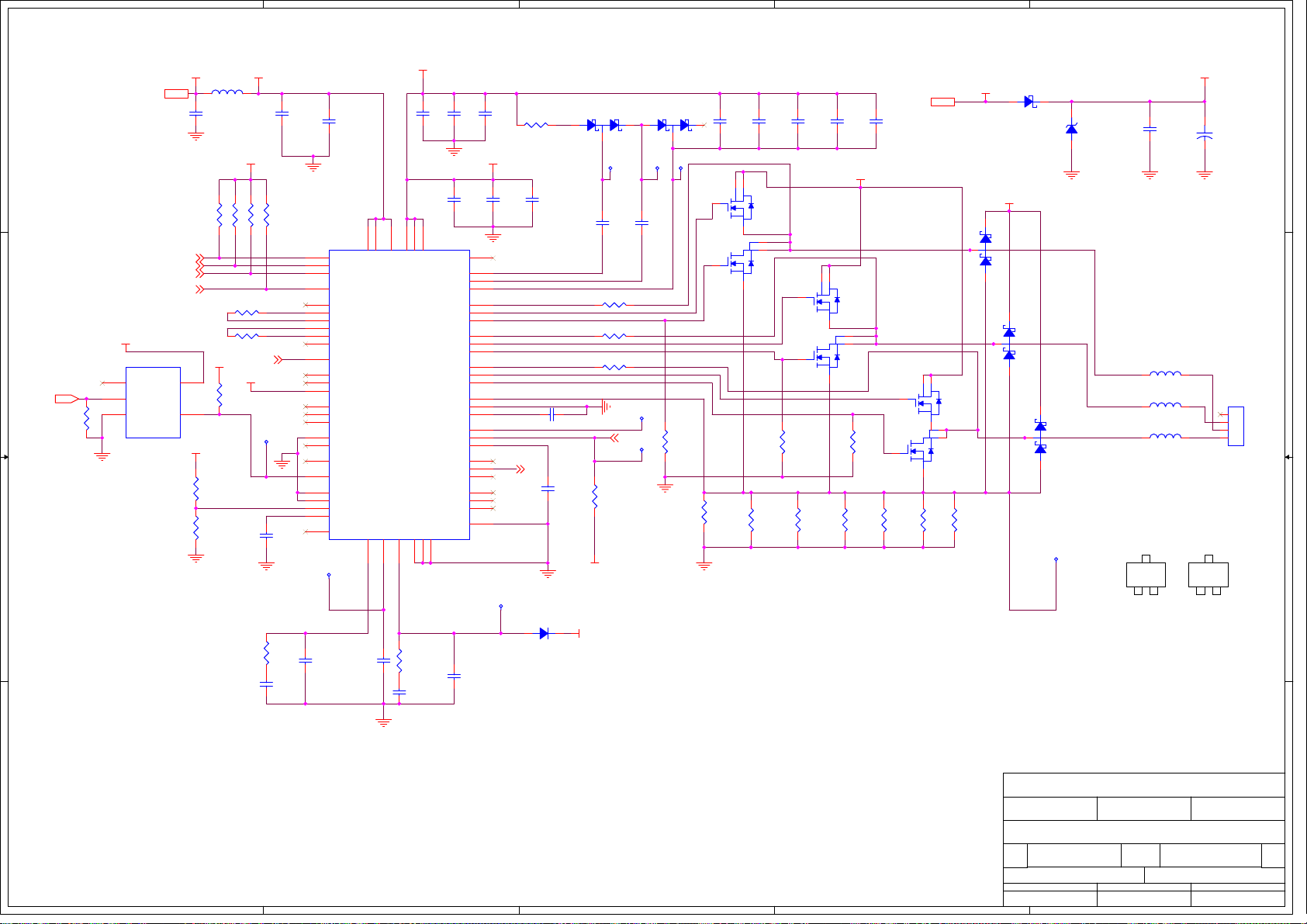
5
4
3
2
1
P5V
P5V
D D
MTRCLK
MTRDATA
MTRSELZ
MTRPWM
C C
MTRRSTZ
B B
R69
1K
DDP3P3V
U12
1
NC
2
A
3
GND
74LVC1G07
VCC
Y
SSI_VDD
5
4
SSI_VDD
L10
120 OHM
C37
1U Z
SSI_VDD P12V
R31
R32
3.3K
3.3K
SSI_VDD
SSI_VDD
R68
4.7K
PORZ
R40
2.74KF
2.26KF
(1206)
C38
4.7U Z
(1206) (1210)
R33
R34
3.3K
3.3K
AIN WHSD
R36
AOUT
1K
ERRN
ERR PV
R37
1K
RSV
TP20
VREFIN
2XVREF
C52
0.1U Z
SSI_RC
R50
3K
(0805)
C56
2.2U Z
11
10
9
64
38
37
36
35
34
33
24
19
15
14
18
17
16
32
31
20
49
39
40
42
43
12
TP21
C53
0.1U Z
0.1U Z
U13
SCLK
SDATA
SDEN
PWMIN
SUM
AIN
ADUT
ERRN
ERR
SOUT
RSV
PRG
PRI
PREG
NRG
NRC
NREG
ISET
GLS
RETZ
PORZ
PWNSB
PMWLSB
VREFIN
2XVREF
FP
C42
C54
330P J
P12V
C39
1U Z C46
(0805) (0805)(0805)
47
46
VCK5
48
45
V5
V12
VCK12
SSI-32H6742T
59
VM122VM2
RC51CVCO50VMAG1AGND121AGND230AGND3
60
CVCO
R51
150K
C57
2700P K
SWG
PUMPZ
PUMP
WHSD
WLSD
VHSD
VLSD
UHSD
ULSD
RSM
SGND
CRH
AMUX
DMUX
CCLK
GPA
VCMA
GNA
GPB
VCMB
GNB
DGND
PW
CP
PU
PV
C40
1U Z
C59
0.1U Z
5
6
7
8
61
53
52
62
55
54
63
57
56
58
44
2
41
3
4
26
23
25
29
27
28
13
VMAG
C55
270P J
C41
4.7U Z
0.1U Z
PUMPZ
PUMP
CP
PW
WLSD
VHSD
VLSD
PU
UHSD
ULSD
RSM
CRH
CCLK
TP22
C60
R30
300
(1/8W)
C61
0.1U Z
RSV
1 2
D7
1N4148
P12V_P
C50
120P J
SSI_AMUX
C51
100P J
D2
R35
R38
R39
SSI_VDD
SSI_VDD
3
BAT54SW
PUMPN2
TP3
C48
0.01U K
100
100
100
MTRDMUX
TP25
R41
3.3K
21
TP24
D3
PUMPN1
TP4
C49
0.01U K
P12V
C44
3
BAT54SW
TP5
C43
21
0.1U Z
5
0.1U Z
C45
0.1U Z
0.1U Z
V12A
C47
0.1U Z
4
Q5B
3 6
7
8
2
Q5A
FDS6930A
1
4
Q6B
5
3 6
7
8
2
Q6A
1
FDS6930A
R43
NC_R0805R49
R72
10M
R44
NC_R0805
R71
10M
R42
NC_R1206
(1206) (0805) (0805) (0805) (0805) (0805) (0805)
R73
10M
R45
NC_0805
4
2
FDS6930A
Q7A
R46
1
5
1
RSM
0.1U Z
2
C62
200 OHM
200 OHM
200 OHM
V12A
12
+
(80.10623.141)
MDY1
MDY2
MDY3
Motor Drive
C/A
3
SOT-323
2
1
AC
C58
10U K
35V
20K2002004
J4
1
2
3
4
D8 RB051L-40
P12V
1 2
(3A, 40V)
(4.6x2.6)
(ROHM)
(83.3R002.08P)
V12A
21
D4
BAT54SW
3
21
D5
BAT54SW
3
Q7B
7
3 6
R47
1
8
R48
1
3
21
D6
BAT54SW
TP23
D9
15V,1.5W,5%
(1SMB5929BT3)
1 2
(ONSEMI)
(83.15R03.03D)
MDY1A
MDY2A
MDY3A
P45
L11
L12
L13
C/A
3
SOT-323
1
C
A
SSI COLOR WHEEL DRIVE CIRCUIT
A A
5
4
3
2
Benq Corporation
Project Code
99.J5877.001
Title
Size Document Number R ev.
PCB P/N
<Size>
48.J5802.S01
Tuesday, January 14, 2003
Date: Sheet of
Prepared By
ANGEL HU
Model Name
HT720G
DMD BOARD
PCB Rev.
S01
Reviewed By Approved By
ALEX HY TSENG BEN CHEN
OEM/ODM Model Name
99.J5877.R22-C3-304-002
88
1
NA
0
Page 88

5
OP_A[0..23]
D D
OP_ENABLE
C C
OCLK_OUT
OP_A16
OP_A17
OP_A18
OP_A19
OP_A20
OP_A21
OP_A22
OP_A23
OP_A8
OP_A9
OP_A10
OP_A11
OP_A12
OP_A13
OP_A14
OP_A15
OP_A0
OP_A1
OP_A2
OP_A3
OP_A4
OP_A5
OP_A6
OP_A7
R14 10
R15 10
R16 10
R17 10
R18 10
R19 10
R20 10
R21 10
R22 10
R23 10
R24 10
R25 10
R26 10
R27 10
R28 10
R29 10
OP_ENABLE
R30 10
R31 10
R32 10
R33 10
R34 10
R35 10
R36 10
R37 10
R38 10
4
IN_OP_A8
IN_OP_A9
IN_OP_A10
IN_OP_A11
IN_OP_A12
IN_OP_A13
IN_OP_A14
IN_OP_A15
IN_OP_A16
IN_OP_A17
IN_OP_A18
IN_OP_A19
IN_OP_A20
IN_OP_A21
IN_OP_A22
IN_OP_A23
IN_OP_A0
IN_OP_A1
IN_OP_A2
IN_OP_A3
IN_OP_A4
IN_OP_A5
IN_OP_A6
IN_OP_A7
+V_DAC
1
G0
2
G1
3
G2
4
G3
5
G4
6
G5
7
G6
8
G7
9
G8
10
G9
11
BLACK
12
SYNC
SYNC
R11
10K
OCLK_OUT_INPUT
+V_DAC
R2
51K
RST_DAC
PWR_SAVE
38
37
39
R948R847R746R645R544R443R342R241R140R0
ADV7123
U1
RST
PSAVE
COMP
VREF
VAA
VAA
GND
GND
VAA13B014B115B216B317B418B519B620B721B822B923CLOCK
24
IOR
IOR
IOG
IOG
IOB
IOB
3
+3VA+5VA
+5VA
R4 560
+V_DAC
C16
VREF
36
COMP
35
34
33
32
31
30
29
28
27
26
25
0.1U Z
C17
0.1U Z
OUT_R
OUT_G
OUT_B
R8
R9
75
75
+3VA
R1
R3 NC
R5
R6 0
R7 0
R10
75
2
0
0
BAV99
DN1
C11
4.7U K
OUT_RED
OUT_GREEN
OUT_BLUE
+V_DAC
2
3
1
C12
0.047U K
2
3
BAV99
1
DN2
0.047U K
6
1
7
2
8
3
9
4
10
5
C13
0.047U K
J4
2022012015
+V_DAC
C14
11
12
13
14
15
1
C15
0.047U K
OP_VSYNC
B B
OP_HSYNC
OP_VSYNC
OP_HSYNC
R12 75
R13
75
VSYNC_OUT
HSYNC_OUT
Optical Points
OP2
OP1
OP
OP
OP3
OP
OP4
OP
OP5
OP
OP6
OP
OP7
OP
Screw Holes
OP8OPOP9
OP
1
5
4
3
2
A A
H1
HOLE-V8
5
9
8
7
6
5
4
3
2
H2
HOLE-V8
1
9
8
7
6
5
4
3
2
H3
HOLE-V8
4
1
9
8
7
6
5
4
3
2
H4
HOLE-V8
1
9
8
7
6
5
4
3
2
H5
HOLE-V8
1
9
8
7
6
3
5
4
3
2
H6
HOLE-V8
1
9
8
7
6
Benq Corporation
Project Code
Title
Size Document Number R ev.
<Size>
Date: Sheet
2
OP10
OP
99.J5877.001
PCB P/N
48.J5824.S02 S02
Wednesday, January 15, 2003
Prepared By
ANGEL HU
OP12OPOP13
OP11
OP
OP
Model Name
HT720G
DMD BOTTOM BOARD
PCB Rev.
Reviewed By Approved By
ALEX HY TSENG
OP14
OP
OEM/ODM Model Name
99.J5877.R22-C3-304-003
12
1
NA
0
of
BEN CHEN
Page 89
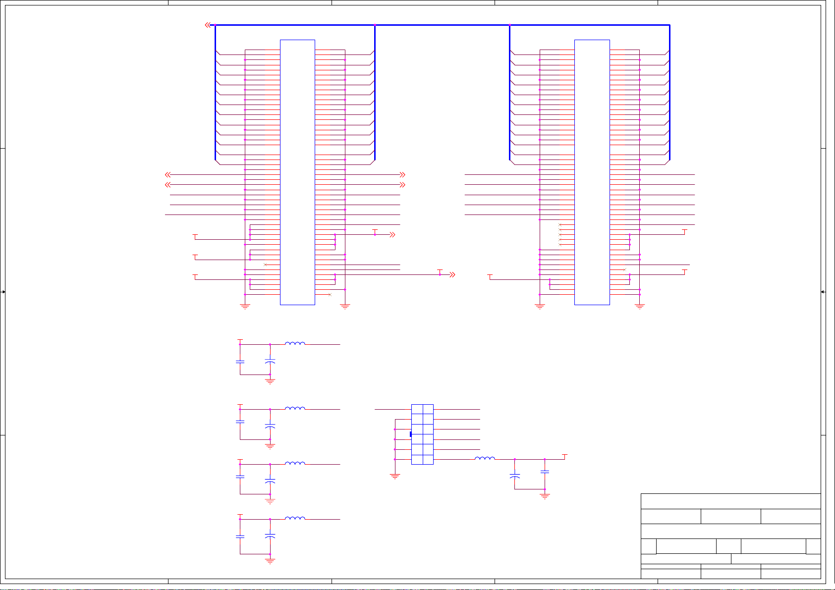
5
OP_A[0..23]
D D
OCLK_OUT
OP_ENABLE
C C
OCLK_OUT
OP_ENABLE
SDA
SCL
POWER
(CLK_OUT)
(OP_ENABLE)
+3VS
+5VS
+12VA
OP_A23
OP_A21
OP_A19
OP_A17
OP_A15
OP_A13
OP_A11
OP_A9
OP_A7
OP_A5
OP_A3
OP_A1
4
J1
1
3
5
7
9
11
13
15
17
19
21
23
25
27
29
31
33
35
37
39
43
45
47
49
51
53
55
57
59
61
63
65
67
69
71
73
75
77
79
81
83
85
87
89
91
93
95
97
99
1
3
5
7
9
11
13
15
17
19
21
23
25
27
29
31
33
35
37
39
43
45
47
49
51
53
55
57
59
61
63
65
67
69
71
73
75
77
79
81
83
85
87
89
91
93
95
97
99
20C1001100
2
2
4
4
6
6
8
8
10
10
12
12
14
14
16
16
18
18
20
20
22
22
24
24
26
26
28
28
30
30
32
32
34
34
36
36
38
38
40
40
44
44
46
46
48
48
50
50
52
52
54
54
56
56
58
58
60
60
62
62
64
64
66
66
68
68
70
70
72
72
74
74
76
76
78
78
80
80
82
82
84
84
86
86
88
88
90
90
92
92
94
94
96
96
98
98
100
100
OP_A22
OP_A20
OP_A18
OP_A16
OP_A14
OP_A12
OP_A10
OP_A8
OP_A6
OP_A4
OP_A2
OP_A0
OP_HSYNC
OP_VSYNC
LAMPLITZ
DLP_RESETZ
POWERON
PWRGOOD
+3VA
SYNCVALID
Ballast_Ctrl
+3VA
3
OP_HSYNC
OP_VSYNC
+5VA
+5VA
OCLK_OUT
OP_ENABLE
SDA
SCL
Ballast_Ctrl
+12VA
OP_A23
OP_A21
OP_A19
OP_A17
OP_A15
OP_A13
OP_A11
OP_A9
OP_A7
OP_A5
OP_A3
OP_A1
(CLK_OUT)
(OP_ENABLE)
1
3
5
7
9
11
13
15
17
19
21
23
25
27
29
31
33
35
37
39
43
45
47
49
51
53
55
57
59
61
63
65
67
69
71
73
75
77
79
81
83
85
87
89
91
93
95
97
99
20C1001100
2
J2
1
3
5
7
9
11
13
15
17
19
21
23
25
27
29
31
33
35
37
39
43
45
47
49
51
53
55
57
59
61
63
65
67
69
71
73
75
77
79
81
83
85
87
89
91
93
95
97
99
2
2
4
4
6
6
8
8
10
10
12
12
14
14
16
16
18
18
20
20
22
22
24
24
26
26
28
28
30
30
32
32
34
34
36
36
38
38
40
40
44
44
46
46
48
48
50
50
52
52
54
54
56
56
58
58
60
60
62
62
64
64
66
66
68
68
70
70
72
72
74
74
76
76
78
78
80
80
82
82
84
84
86
86
88
88
90
90
92
92
94
94
96
96
98
98
100
100
OP_A22
OP_A20
OP_A18
OP_A16
OP_A14
OP_A12
OP_A10
OP_A8
OP_A6
OP_A4
OP_A2
OP_A0
OP_HSYNC
OP_VSYNC
LAMPLITZ
DLP_RESETZ
POWERON
PWRGOOD
SYNCVALID
+3VA
+5VA
(For HD2)(For HD2)
(For HD2)(For HD2)
(For HD2)(For HD2)
1
+3VA
+5VS
+5VA
+3VS
C8
0.1U K
C6
0.1U K
C4
0.1U K
C10
0.1U K
4
B B
A A
5
L4
12
500 OHM
C7
+
22U
35V
L3
12
500 OHM
C5
+
22U
35V
L2
12
500 OHM
C3
+
22U
35V
12
500 OHM
C9
+
22U
35V
(1206)
L5
(1206)
(1206)
(1206)
3VA
5VS
5VA
3VS
10
11
12
7
8
9
J3
7
8
9
10
11
12
20E1006206
3
1
2
3
4
5
6
3VS
2
5VS
3
5VA
4
POWER
5
6
12VA
L1
500 OHM
(1206)
12
C1
+
22U
35V
C2
0.1U K
+12VA
Benq Corporation
Project Code
99.J5877.001
Title
Size Document Number R ev.
PCB P/N
<Size>
48.J5824.S02 S02
Wednesday, January 15, 2003
Date: Sheet
Prepared By
2
ANGEL HU
Model Name
HT720G
DMD BOTTOM BOARD
PCB Rev.
99.J5877.R22-C3-304-003
Reviewed By Approved By
ALEX HY TSENG
1
OEM/ODM Model Name
NA
of
22
BEN CHEN
0
3VA3VA
1
Page 90

5
4
3
120-Pin B2B Connectors
2
1
Graphics_ADC_AD9883
D_INA[0..23]
D D
HSYNC
VSYNC
Y/R
PB/G
PR/B
+5V_AD
+3VD
Y/R
PB/G
PR/B
VSYNC
HSYNC
+3VD
D_VSYNC
D_HSYNC
DIN_CLK
DVI_PDO
SDA
SCL
D_INA[0..23]
D_VSYNC
D_HSYNC
DIN_CLK
DVI_PDO
SDA
SCL
D_INA[0..23]
D_VSYNC
D_HSYNC
DIN_CLK
SDA
SCL
Trigger/3D/Thermal/RS232
+12VA+5VS
+5VS
IR
IR
+12VAIR
+5V_AD
DVI_CLK
TRIGGER
Graphics_Inputs
Y/R
PR/B
PB/G
VSYNC
HSYNC
PC_VS
C C
+5V_AD
+5V_AD
PC_HS
PC_GREEN
PC_RED
PC_BLUE
MUX_SEL_Q
+5V_MUX
+5V_MUX
YpYcG
PbCbB
PrCrR
YpYcG
PbCbB
PrCrR
MUX_SEL_P
MUX_SEL
1_Graphics Inputs
Video Inputs
B B
MUX_BUFFER
+5V_AD
+5V_MUX
MUX_BUFFER
+5V_MUX
+5V_AD
2_Video Inputs
A A
5
O_COMP_CR
O_COMP_CB
O_COMP_Y
L_Y_G
O_COMP_Y
O_COMP_CB
O_COMP_CR
O_COMP_Y
O_COMP_CB
O_COMP_CR
L_Y_G
L_Pb
L_Pr
L_Pb
L_Pr
L_Pr
L_Pb
L_Y_G
COMPOSITE
CB1
CR1
COMPOSITE
Y
C
+5V_AD
Y_RCA
Cb_RCA
Cr_RCA
+3VD
4
Y1
Y
C
3_Graphics ADC AD9883
PC_VS
PC_HS
PC_GREEN
PC_RED
PC_BLUE
MUX_SEL_Q MUX_SEL_Q
+3VD
Video Decoder SAA7118E
YpYcG
PbCbB
PrCrR
Y1
DVI
+5V_AD
8_DVI INPUT&RECEIVER
DI_IN[2..9]
DI_27M_CLK
DI_VSYNC
DI_HSYNC
CB1
CR1
COMPOSITE
Y
RESET_DEC
C
PC_VS
PC_HS
PC_GREEN
PC_RED
PC_BLUE
+5V_AD
+3VD
SDA
SCL
DVI_CLK
DVI_CLK
DVI_SCDT
D_HSYNC
D_VSYNC
D_INA[0..23]
DVI_ACTDATA
DVI_PDO
SDA
SCL
DVI_SCDT
DVI_ACTDATA
DI_IN[2..9]
DI_27M_CLK
DI_VSYNC
DI_HSYNC
RESET_DEC
DVI_PDO
DVI_SCDT
DVI_ACTDATA
DI_IN[2..9]
DI_27M_CLK
DI_VSYNC
DI_HSYNC
RESET_DEC
SPAREI
SPAREO
MUX_SEL_Q
CPU_TXD0
+3VD
CPU_RXD0
+5V_AD
5_Video Decoder SAA7118E
MUX_SEL
MUX_SEL_P
MUX_BUFFER
CPU_TXD0
3
CPU_RXD0
7_120Pin B2B Connector
MUX_SEL
MUX_SEL_P
MUX_BUFFER
+3VD
+5VS
+5V_AD
+12VA
+3VD
+5VS
+5V_AD
2
+12VA
TRIGGER
TRIGGER
CPU_TXD0
CPU_RXD0
6_Trigger/3D/Thermal/RS232
Benq Corporation
Project Code
99.J5877.001
Title
Size Document Number R ev.
PCB P/N
<Size>
48.J5810.S02
Monday, February 17, 2003
Date: Sheet
Prepared By
ANGEL HU
Model Name
HT720G
CONNECTOR BOARD
PCB Rev.
99.J5877.R22-C3-304-004
S02
Reviewed By Approved By
ALEX HY TSENG BEN CHEN
1
OEM/ODM Model Name
18
NA
0
of
Page 91
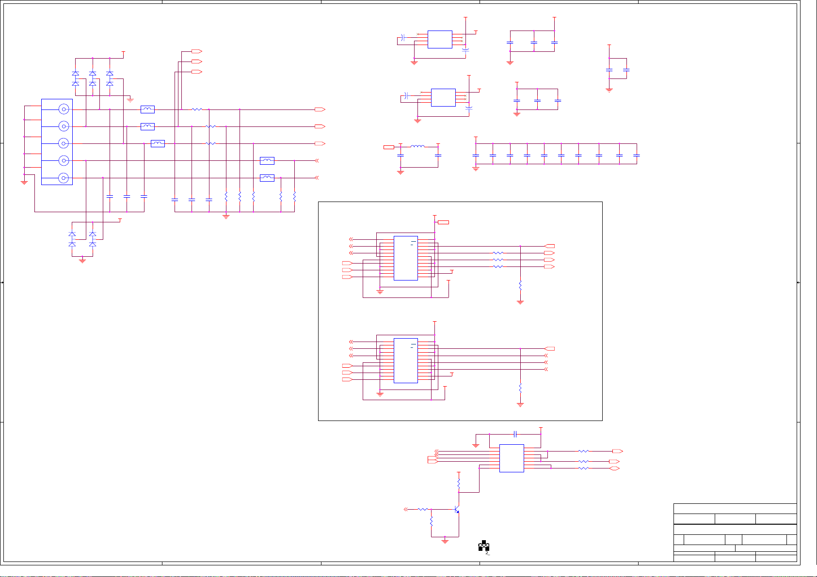
5
+5V_AD
2
2
D1
D D
J1
6
GND
7
GND
8
GND
9
GND
10
GND
BNC_5_IN_1
C C
BAV99
1
1
1
2
2
3
3
4
4
5
5
2
D4
BAV99
3
1
2
D2
D3
BAV99
BAV99
3
1
HS_B
2
1
VS_B
D5
BAV99
3
1
Pb_Cb_B
C137
0.1UF
+5V_AD
Pr_Cr_R
C138
0.1UF
L2
1
FCB3216K
L3
1
FCB3216K
0.1UF
2
2
L4
1
FCB3216K
C139
2
Y_Y_G
3
3
0.1UF
L_Y_G
L_Pb
L_Pr
18
R112
R113
R114
C140
C141
0.1UF
18
18
0.1UF
4
YpYcG
YpYcG
PbCbB
PbCbB
PrCrR
L5 FCB3216K
2
1
2
1
L6 FCB3216K
12
12
12
12
R1
R2
56
56
C142
R4
R3
4.7K
56
BNC_HS
BNC_VS
12
R5
4.7K
O_R
O_G
O_B
O_COMP_CR
O_COMP_CB
O_COMP_Y
+5V_AD
3
+
1
2
3
4
5
6
7
8
9
10
11
C135
10UF/16
+5V_AD
IN0A
DGND
IN1A
GND
IN2A
VCC
VEE
IN2B
GND
IN1B
GND
IN0B12VCC
U16
1
NC
CAPP+
2
12
CAP+
3
GND
CAPP-
CAP-4VOUT
+
C1
10UF/16
1
CAP+
2
12
3
CAP-
L1
Z1000/100MHZ
C2
0.1UF
+5V_MUX
U2
24
VCC
23
OE
22
SEL A/B
21
VCC
20
OUT0
19
VEE
18
OUT1
17
VCC
16
OUT2
15
VEE
14
DVCC
13
AD8183
This MUX is for seletion between
BNC_YPbPr and DSUB_BNC_RGB
+5V_MUX
OSC
ICL7660A
U1
NC
CAP+
GND
CAP-4VOUT
ICL7660A
+5V_MUX
0.1UF
V+
LV
OSC
C3
-5V
V+
LV
+5V_MUX
+5V_AD
2
-5V_RGB
+5V_AD
8
7
6
5
C136
+
10UF/16
1 2
-5V
+5V_AD
8
7
6
5
C4
+
10UF/16
1 2
+5V_MUX
C5
0.1UF
C6
0.1UF
C22
0.1UF
-5V
C7
0.1UF
C15
0.1UF
C8
0.1UF
C23
0.1UF
C16
0.1UF
-5V_RGB
C9
0.1UF
C24
0.1UF
C17
0.1UF
C10
0.1UF
C11
0.1UF
+5V_AD
C12
0.1UF
C18
0.1UF
C13
0.1UF
C19
0.1UF
C14
0.1UF
1
For AD8183
MUX_SEL
OUT_Y/R
OUT_PB/G
OUT_PR/B
R6 75
1 2
R7 75
1 2
R8 75
1 2
12
R9
1K
MUX_SEL
Y/R
PB/G
PR/B
U3
L_Y_G
PC_RED
PC_BLUE
PC_GREEN
L_Pb
L_Pr
B B
A A
5
4
1
2
3
4
5
6
7
8
9
10
11
MUX_SEL_P
24
IN0A
VCC
23
DGND
OE
22
IN1A
SEL A/B
21
GND
VCC
20
IN2A
OUT0
19
VCC
VEE
18
VEE
OUT1
17
IN2B
VCC
16
GND
OUT2
IN1B
VEE
GND
DVCC
IN0B12VCC
AD8183
This MUX is for seletion between
BNC-RGB and DSUB_RGB
PC_HS
PC_VS
R14 1K
3
15
14
13
BNC_HS
BNC_VS
+5V_AD
-5V_RGB
R13
5.1K
SEL
1
R15
10K
+5V_MUX
32
2N3904
MUX_SEL_P
SEL_HV
Q1
2N3904
1_B
1:BNC-HV
OUT
0:DSUB-HV
OUT
3_C
2_E
U4
7
GND
2
A0
5
A1
12
A2
9
A3
1
OE0
4
OE1
74126(73.74126.0HB)
C25
0.1UF
MUX_SEL_P
O_G
O_B
O_R
12
R10
10K
+5V_MUX
14
VCC
O0
O1
O2
O3
OE2
OE3
O_HS
O_VS
MUXPP
2
R11 75
1 2
R12 75
1 2
R73 0
1 2
HSYNC
VSYNC
MUX_SEL_Q
Benq Corporation
Project Code
99.J5877.001
Title
Size Document Number Rev.
PCB P/N
<Size>
Monday, February 17, 2003
Date: Sheet
Prepared By
ANGEL HU
Model Name
CONNECTOR BOARD
48.J5810.S02
1
OEM/ODM Model Name
HT720G
PCB Rev.
S02
Reviewed By Approved By
ALEX HY TSENG BEN CHEN
NA
99.J5877.R22-C3-304-004
of
28
0
3
6
11
8
13
10
Page 92

5
L39
42 OHM
L40
42 OHM
J3
RCA-JACK
1
1
2
2
J4
S-VIDEO
1
2
3
4
5
6
7
8
9
10
11
2
1
RCA_IN
SVIDEO_Y
3
3
4
4
SVIDEO_C
U5
IN0A
VCC
DGND
IN1A
SEL A/B
GND
VCC
IN2A
OUT0
VCC
VEE
VEE
OUT1
IN2B
VCC
GND
OUT2
IN1B
VEE
GND
DVCC
IN0B12VCC
AD8183
OE
L41
D D
C C
B B
42 OHM
YCC
CBB
L_Pr
L_Pb
L_Y_G
R124
R125
R126
0
0
0
5
6
YCC_U5
CBB_U5
CRR_U5CRR
5
6
C143
0.1UF
(open)
L14
1
FCB3216K
C145
0.1UF
(open)
L17
1
FCB3216K
C147
0.1UF
24
23
22
21
20
19
18
17
16
15
14
13
L13
1
FCB3216K
+5V_AV
4
+5V_AD
D11
BAV99
2
2
-5V_AV
2
OUT_YY
OUT_CC
MUX_YP
MUX_PB
MUX_PR
+5V_AD
1
OUT_COMP
(open)
C144
0.1UF
D15
BAV99
1
(open)
C146
0.1UF
D17
BAV99
1
(open)(open)
C148
0.1UF
3
3
1 2
3
R36 0
1 2
R37 0
1 2
R38 0
1 2
2
R21 18
1 2
2
+5V_AD
R23 18
2
+5V_AD
R28
1 2
18
+5V_AD
12
R70
56
12
R22
56
12
R25
56
12
R30
56
12
12
R71
R72
56
56
Y
C
12
R39
1K
3
COMPOSITE
2
4
6
MUX_BUFFER
O_COMP_Y
O_COMP_CB
O_COMP_CR
J5
2
4
6
RCA 3 IN 1
2
+5V_AD
2
2
D12
BAV99
3
1
Cr
1
1
3
3
5
5
Cb
2
D13
D14
BAV99
BAV99
3
3
ERRORON1
1
1
ERRORON2
L15
1
FCB3216K
C149
0.1UF
(open) (open)
L16
1
FCB3216K
C151
0.1UF
(open) (open)
C153
0.1UF
L18
1
FCB3216K
YC
The voltage level of CB/CR is
+0.35~-0.35 , add one diode
to prevent uncertain 'ON'
error
D16
2
2
C150
0.1UF
2
C152
0.1UF
2
BAV99
CRR
1
3
CBB
YCC
C154
0.1UF
R24 18
1 2
R27
1 2
R31 18
1 2
18
1
R26
56
R29
56
R35
56
CR1
CB1
Y1
12
12
12
(open) (open)
This MUX is BUFFER of
Composite and
S-Video
C31
0.1UF
+5V_MUX
-5V_AV
C26
+
10UF/16
A A
CAPP-
CAPP+
12
U6
1
NC
2
CAP+
3
GND
CAP-4VOUT
5
ICL7660A
OSC
V+
LV
+5V_AD
8
7
6
5
C38
+
10UF/16
1 2
-5V_AV
C29
0.1UF
C30
0.1UF
4
+5V_MUX
12
+
10UF/16
(open) (open)
(open)
Open if -5V is not necessary
L19
Z1000/100MHZ
12
C27
+
10UF/16
C28
C32
0.1UF
3
C33
0.1UF
For AD8183
C34
0.1UF
+5V_AV
C35
0.1UF
C36
0.1UF
+5V_AD
C37
0.1UF
Benq Corporation
Project Code
99.J5877.001
Title
Size Document Number R ev.
PCB P/N
<Size>
48.J5810.S02
Monday, February 17, 2003
Date: Sheet
Prepared By
2
ANGEL HU
Model Name
HT720G
CONNECTOR BOARD
PCB Rev.
99.J5877.R22-C3-304-004
S02
Reviewed By Approved By
ALEX HY TSENG BEN CHEN
1
OEM/ODM Model Name
NA
0
of
38
Page 93

5
D D
TP19
E1
Y/R
C C
PB/G
PR/B
HSYNC
VSYNC
1
TP20
E1
1
TP21
E1
1
Y/R
PB/G
TP22
E1
1
PR/B
R43
R44
R45
220
220
220
For AD8185
R=75
B B
4
AD_G2
AD_G7
AD_G1
AD_G6
AD_G5
AD_G0
AD_G4
AD_G3
C39
AD_RIN
47NF
C41
AD_GIN
47NF
C42
AD_BIN
47NF
C44
AD_SOGIN
1NF
12
R46
TP23
1K
E1
1
12
R48
51K
+3VD
H_SYNC
TP1
E1
TP3
E1
TP5
E1
TP7
E1
TP9
E1
TP11
E1
TP13
E1
TP15
E1
LP1 120 OHM
D_INA8
1
8
D_INA9
2
7
D_INA10
3
6
D_INA11
4 5
1
2
3
4 5
D_INA12
8
D_INA13
7
D_INA14
6
D_INA15
LP2 120 OHM
TP17
AD_R0
AD_R1
1
E1
79
80
77
VDD78VDD
GND
1
GND
2
G7
3
G6
4
G5
5
G4
6
G3
7
G2
8
G1
9
G0
10
GND
11
VDD
12
B7
13
B6
14
B5
15
B4
16
B3
17
B2
18
B1
19
B0
20
GND
GND21VDD22VDD23GND24GND25VD26VD27GND28COAST29HSYNC30VSYNC31GND32FILT33PVD34PVD35GND36MIDSCV37CLAMP38VD39GND
AD_B0
AD_B1
AD_B2
AD_B3
AD_B4
AD_B5
AD_B6
AD_B7
1
1
1
1
1
1
1
1
AD_R2
AD_R3
AD9883
AD_R4
U7
AD_R5
AD_R6
1
2
3
4 5
1
2
3
AD_R7
4 5
DATACK
69
68
R770R671R572R473R374R275R176R0
VDD
+3VC_A2D
FILT
3
(open) (open) (open) (open)
CN1
22P
5 4
LP4 120 OHM
LP3 120 OHM
HSOUT
SOGOUT
67
66
65
GND
HSOUT
DATACK
SOGOUT
REF BYPASS
1 2
R47
2.7K
8 1
7 2
6 3
8
7
6
8
7
6
1
VSOUT
61
63
64
62
VD
GND
GND
GND
VSOUT
VD
SDA
SCL
A0
RAIN
GND
VD
VD
GND
SOGIN
GAIN
GND
VD
VD
GND
BAIN
VD
GND
40
LP6 120 OHM
1
2
3
4 5
1
2
3
4 5
LP5 120 OHM
FLT
C45
82NK 16V
C46
8200P K
CN2
22P
TP18
E1
60
59
58
57
56
55
54
53
52
51
50
49
48
47
46
45
44
43
42
41
MIDSCV
5 4
R41 33
1 2
R42 33
1 2
REF_BYPASS
8
7
6
8
7
6
CN5
7 2
6 3
D_INA16
D_INA17
D_INA18
D_INA19
D_INA20
D_INA21
D_INA22
D_INA23
C43 0.1UF
817263
8 1
+3VB_A2D
D_INA0
D_INA1
D_INA2
D_INA3
CN3
22P
C40
0.1UF
(open)
7 2
6 3
5 4
6 3
5 4
D_INA4
D_INA5
D_INA6
D_INA7
54
22P
CN4
22P
8 1
(open)
7 2
8 1
7 2
6 3
5 4
SDA
SCL
CN6
22P
8 1
TP2
2
E1
1
TP4E1
1
TP6
1
E1
TP8E1
1
TP10
1
E1
E1
TP12
1
TP14
1
E1
TP16
1
E1
D_HSYNC
D_VSYNC
0
R115
U22_ADCLK
U22_DVICLK
1
2
3
4
5
6
7
8
9
10
11
R118
U23_CAP-
AD_CLK
DVI_CLK
1
1
1
1
1
1
1
0
R117
TP24
TP25
E1
TP26
E1
TP27
E1
TP28
E1
TP29
E1
TP30
E1
E1
AD_CLK
R116
U22
IN0A
DGND
IN1A
SEL A/B
GND
IN2A
VCC
VEE
IN2B
GND
IN1B
GND
IN0B12VCC
AD8183
0
C188
12
+
10U
16V
D_HSYNC
D_VSYNC
SDA
SCL
0
VCC
OE
VCC
OUT0
VEE
OUT1
VCC
OUT2
VEE
DVCC
U23_CAP
D_INA[0..23]
24
23
22
21
OUTDINCLK
20
19
18
17
16
15
14
13
U23
1
NC
2
CAP+
3
GND
CAP-4VOUT
+5V_ADDVI
-5V_ADDVI
OSC
ICL7660S 5V
1
C155
22P J
<Spec>
C187
0.1U Z
DVI_PDO
DIN_CLK
30 OHM
L30
C156
22P J
<Spec>
+5V_AD
C178
0.1U Z
-5V_ADDVI
+5V_AD
8
V+
7
6
LV
5
C189
+
10U
1 2
16V
-5V_ADDVI +5V_ADDVI
+3VD
+3VD
0.1UF
U8
C53
4.7UF/16
LD1117/SOT
3
2
VOUT
VIN
GND
1
12
+
C54
10UF/16
0.1UF
C56
C55
0.1UF
C57
0.1UF
C58
0.1UF
C59
0.1UF
C60
0.1UF
C61
0.1UF
C62
0.1UF
C63
0.1UF
C64
0.1UF
+5V_AD +3VB_A2D
C47
C48
0.1UF
0.1UF
C50
C49
0.1UF
0.1UF
C51
C52
0.1UF
C179
0.1U Z
C180
0.1U Z
C181
0.1U Z
C182
0.1U Z
C183
0.1U Z
C184
0.1U Z
C185
0.1U Z
C186
0.1U Z
A A
+5V_AD
+5V_AD
5
C65
4.7U/16V
U9
LD1117/SOT
3
VIN
0.1UF
C67
4
+3VC_A2D
C68
0.1UF
3
2
2
VOUT
12
GND
1
+
C66
10UF/16
Benq Corporation
Project Code
99.J5877.001
Title
Size Document Number Rev.
PCB P/N
<Size>
Monday, February 17, 2003
Date: Sheet
Prepared By
48.J5810.S02
ANGEL HU
Model Name
HT720G
CONNECTOR BOARD
PCB Rev.
S02
99.J5877.R22-C3-304-004
Reviewed By Approved By
ALEX HY TSENG BEN CHEN
OEM/ODM Model Name
NA
of
48
1
0
Page 94

5
4
3
2
1
TP31
E1
D D
Y
C
C C
PrCrR
CR1
PbCbB
B B
CB1
YpYcG
Y1
A A
COMPOSITE
5
1
SYIN
C69
47NF
TP40
E1
1
C70
47NF
TP54
E1
1
C74
47NF
TP56
E1
1
C76
47NF
TP57
E1
1
C77
47NF
TP58
E1
1
C78
47NF
TP59
C82
E1
47NF
1
C84
47NF
C97
TP60
47NF
E1
1
C98
47NF
TP61
E1
C105
47NF
1
C106
47NF
S_YIN
S_CIN
C71 47NF
C72 47NF
C73 47NF
C75 47NF
CB1_IN
SOG_Y
SOG_Y_IN
Y_IN
SOG_RCA
RAC_IN
CR1_IN
4
AI1C
AI1D
AI2C
AI2D
AI3C
AI3D
AI4C
AI4D
EXMCLR
TP55
1
E1
C6
B5
A5
TDI
TDO
TRST
M13
FSW
J2
AI11
K1
AI12
K2
AI13
L3
AI14
K3
AI1D
C2
AGND
G4
AI21
G3
AI22
H2
AI23
J3
AI24
H1
AI2D
E3
AI31
F2
AI32
F3
AI33
G1
AI34
F1
AI3D
L2
AGNDA
B1
AI41
D2
AI42
D1
AI43
E1
AI44
D3
AI4D
P3
EXMCLR
M1
AOUT
M2
VSSA0
J4
VSSA1
H3
VSSA2
+3VE
E4
VSSA3
C1
VSSA4
M3
VDDA0
K4
VDDA1
H4
VDDA2
F4
VDDA3
D4
VDDA4
L1
VDDA1A
J1
VDDA2A
G2
VDDA3A
E2
VDDA4A
VSSD2D7VSSD4
VSSD6
F11
D10
+3VD +3VD
I2C BUS SLAVE ADDRESS:
0x42 - W,0x43 - R
U11
LD1117/SOT
+5V_AD
C85
4.7UF/16
3
VIN
+5V_AD
D6
B6
P13
TCK
TMS
VSSD8
VSSD10L5VSSD12L9VDDD2C8VDDD4
J11
GND
1
VOUT
N14
TEST18P2TEST19
C10
3
N13
TEST17
F12
VDDD6
J12
TP36
E1
TP38
E1
C14
D13
TEST12
TEST13N1TEST14N2TEST15N3TEST16
VDDD8
VDDD10M5VDDD12M9VSSD1D5VSSD3D9VSSD5
3.3V_7118
2
12
+
10UF/16
C12
C13
TEST10
TEST11
VSSD7
VSSD9L4VSSD11L8VSSD13
D11
G11
L21
Z1000/100MHZ
C86
+3VD
1
1
B12
B13
B14
TEST5
TEST6
TEST7C3TEST8C4TEST9
U10
SAA7118E
VDDD1C5VDDD3C9VDDD5
L11
L23
Z1000/100MHZ
A12
A13
M12
P12
P11
TEST1
TEST2
TEST3B2TEST4
AMCLK
ALRCLK
AMXCLK
VDDD7
VDDD9M4VDDD11M8VDDD13
VSS(xtal)A4VDD(xtal)B3XTOUTA2XTALOA3XTALIB4ADP8P6ADP7M6ADP6L6ADP5N7ADP4P7ADP3L7ADP2M7ADP1
D12
H12
M11
VDD_XTAL
C81
0.1UF
12
+
10UF/16
+3VD
N11
C87
P10
ASCLK
N9
SDA
XTALO
INT_A
RESET
RTS0
RTS1
L10
P9
P5
M10
N10
N4
CE
SCL
RES
RTS1
RTCO
INT_A
XTALI
R53 820K
24
X1 24.576MHZ
C80
22PF
XTALA
C88
0.1UF
C99
0.1UF
C107
0.1UF
RTS0
13
N5
LLC2
TP32
LLC2
LLC
B11
P4
LLC
XRDY
XCLK
XPD0
XPD1
XPD2
XPD3
XPD4
XPD5
XPD6
XPD7
HPD0
HPD1
HPD2
HPD3
HPD4
HPD5
HPD6
HPD7
ITRDY
CLKEXT
ADP0
P8
C89
0.1UF
C100
0.1UF
C108
0.1UF
E1
1
XTRI
XRV
XRH
XDQ
ITRI
IGP1
IGP0
IGPV
IGPH
IDQ
ICLK
IPD0
IPD1
IPD2
IPD3
IPD4
IPD5
IPD6
IPD7
TP34
TP33
E1
E1
1
1
SCL
XRV
XRH
XRDY
XDQ
XCLK
XPD0
XPD1
XPD2
XPD3
XPD4
XPD5
XPD6
XPD7
L20
NC_L1206
L22
Z1000/100MHZ
C83
NC_C0603
C91
C102
C110
0.1UF
0.1UF
0.1UF
1
1
1
TP42
TP41
E1
1
C92
0.1UF
C103
0.1UF
C111
0.1UF
R49 33
D8
C7
A6
B7
A7
A8
B8
A9
B9
A10
B10
A11
C11
D14
E11
E13
E12
E14
F13
F14
G13
L12
K13
L14
K14
K12
N12
L13
M14
G14
G12
H11
H14
H13
J14
J13
K11
N6
N8
1
C79
22PF
2
XHELP
ANALOG SAA7118E
C90
0.1UF
DIGITAL SAA7118E - CORE
C101
0.1UF
DIGITAL SAA7118E - PERIPHERAL CELLS
C109
0.1UF
2
SDA
SCL
TP35
E1
RESET_DEC
TP37
E1
TP39
E1
E1
1
C93
C104
C112
TP43
E1
1
1 8
2 7
3 6
4 5
RP7 47_RP
1 8
2 7
3 6
4 5
RP8 47_RP
0.1UF
0.1UF
0.1UF
TP44
TP45
E1
E1
1
1
C94
0.1UF
C113
0.1UF
C95
0.1UF
DI_IN2
DI_IN3
DI_IN4
DI_IN5
DI_IN6
DI_IN7
DI_IN8
DI_IN9
+3VE
R50 33
R51 33
R52 33
C96
0.1UF
DI_27M_CLK
12
TP47
TP46
TP48
E1
E1
E1
1
1
1
DI_VSYNC
DI_HSYNC
DI_27M_CLK
TP49
TP50
TP51
TP52
E1
1
TP53
E1
E1
E1
E1
1
1
1
1
Benq Corporation
Project Code
99.J5877.001
Title
Size Document Number Rev.
PCB P/N
<Size>
Monday, February 17, 2003
Date: Sheet
Prepared By
48.J5810.S02
ANGEL HU
Model Name
HT720G
CONNECTOR BOARD
PCB Rev.
S02
99.J5877.R22-C3-304-004
Reviewed By Approved By
ALEX HY TSENG BEN CHEN
DI_IN[2..9]
OEM/ODM Model Name
NA
0
of
58
1
Page 95

5
4
3
2
1
+12VA
+12VA
TRIGGER
GG
2
1
C119
0.1UF
+5VS
FCB3216K
L27
VCC_IR
D D
U12
3
VCC
2
GND
1
VOUT
FM6038TM2
FRONT_IR
C117
0.1UF
R54 47
C118
4.7UF/16
L24
1
FCB3216K
R56 1K
2
TRIGTRIGGER
R57
10K
+
VOUT_TRIGGER
C114
10UF/25
R55
47K
32
2N3904
1
Q3
2N3904
Q2
1
S
2
S
3
S
4
G
Si4431DY
G
1:TURN ON
0:TURN OFF
3_C
8
D
7
D
6
D
5
D
84.04431.037
F1
DR
PICOFUSE
69.42001.021
R74
10K
C115
10UF/25
12
TOUT_12V
+
C116
0.1UF
1
2
3
J6
SCD437
1_B 2_E
R58 130
IR
C C
+5VS
J9
1
2
IR
B B
3
20.D0049.103
C124
0.1UF
C125
0.1UF
C123
0.1UF
RSV+
RSV-
232_C1-
232_C2+
232_C2-
232_C1+
C121
0.1UF
1
2
3
4
5
6
7
SP232
U14
C1+
V+
C1C2+
C2VT2OUT
R2IN8R2OUT
VCC
GND
T1OUT
R1IN
R1OUT
T1IN
T2IN
TX1
RX1
J7
+5VS
C122
0.1UF
16
15
14
13
12
11
10
9
RX
T1OUT
R1IN
+5VS
R61 150/1206
1 2
R62 150/1206
1 2
R59 NC_R1206
1 2
R60 NC_R1206
1 2
2213008001
1
1
2
2
3
3
4
4
D18
D19
27V
27V
RXX1
TXX1
D20
D21
27V
27V
C126
R69
+5VS
R63
1K
R68
1K
47PF/50
1K
A A
CPU_TXD0
CPU_RXD0
CPU_TXD0
CPU_RXD0
R64
100
C127
47PF/50
Benq Corporation
Project Code
99.J5877.001
Title
Size Document Number R ev.
PCB P/N
<Size>
48.J5810.S02
Monday, February 17, 2003
Date: Sheet
Prepared By
ANGEL HU
Model Name
HT720G
CONNECTOR BOARD
PCB Rev.
99.J5877.R22-C3-304-004
S02
Reviewed By Approved By
ALEX HY TSENG BEN CHEN
OEM/ODM Model Name
NA
of
68
0
Page 96

DI_IN[2..9]
5
4
3
2
1
D_INA[0..23]
D D
J8
1
61
2
62
3
63
4
64
5
65
6
66
7
67
8
68
9
69
10
70
11
71
12
72
13
73
14
74
15
75
16
76
17
77
18
78
19
79
20
80
21
81
22
82
23
83
24
84
25
85
26
86
27
87
28
88
29
89
30
90
31
91
32
92
33
93
34
94
35
95
36
96
37
97
38
98
39
99
40
100
41
101
42
102
43
103
44
104
45
105
46
106
47
107
48
108
49
109
50
110
51
111
52
112
53
113
54
114
55
115
56
116
57
117
58
118
59
119
60
120
AMP 120P D0.8
1
2
3
4
5
6
7
8
9
10
11
12
13
14
15
16
17
18
19
20
21
22
23
24
25
26
27
28
29
30
31
32
33
34
35
36
37
38
39
40
41
42
43
44
45
46
47
48
49
50
51
52
53
54
55
56
57
58
59
60
SPA8
SPA9
DVI_SCDT
IR
MUX_SEL
D_VSYNC
D_INA23
D_INA22
D_INA19
D_INA18
D_INA15
D_INA14
D_INA11
D_INA10
D_INA7
D_INA6
D_INA3
D_INA2
DVI_PDO
DVI_ACTDATA
SDA
DI_IN9
DI_IN7
DI_IN5
DI_IN3
DI_VSYNC
R65 NC_R0603
1 2
R66 0
1 2
SPAREI
MUX_SEL_Q
+5VS
C128
0.1UF
+5VS
61
SPA7
62
63
64
65
66
67
68
69
70
71
72
73
74
75
76
77
78
79
80
81
82
83
84
85
86
87
88
89
90
91
92
93
94
95
96
97
98
99
100
101
102
103
104
105
106
107
108
109
110
111
112
113
114
115
116
117
118
119
120
TRIGGER
MUX_SEL_P
CPU_RXD0
MUX_BUFFER
C C
B B
+5V_AD
+5V_AD
C129
0.1UF
12
+
C130
10UF/16
SPAREO
L25
1
FCB3216K
CPU_TXD0
D_HSYNC
DIN_CLK
D_INA21
D_INA20
D_INA17
D_INA16
D_INA13
D_INA12
D_INA9
D_INA8
D_INA5
D_INA4
D_INA1
D_INA0
SCL
DI_IN8
DI_IN6
DI_IN4
DI_IN2
RESET_DEC
DI_HSYNC
DI_27M_CLK
R67 NC_R0603
1 2
2
C131
0.1UF
5VA
Optical Points
OP1
OP
OP8
OP
234
678
234
678
234
678
234
678
OP2OPOP3
OP
OP9OPOP10
OP
5
1
9
5
1
9
5
1
9
5
1
9
OP4
OP
OP11
OP
H1
HOLE-V8
H3
HOLE-V8
H5
HOLE-V8
H7
HOLE-V8
OP5OPOP6OPOP7
OP
OP12OPOP13
OP
1
1
1
OP14
OP
OP15
OP16
OP
OP
H2
2
3
4
5
9
5
9
5
9
HOLE-V8
6
7
8
H4
2
3
4
HOLE-V8
6
7
8
H6
2
3
4
HOLE-V8
6
7
8
+5V_AD
C132
0.1UF
A A
U15
LD1117/SOT
3
VIN
1
GND
VOUT
2
+3VD
C134
10UF/16
+3VD
12VA
L26
1
FCB3216K
C133
0.1UF
+12VA
+12VA
Benq Corporation
Project Code
99.J5877.001
Title
Size Document Number R ev.
PCB P/N
<Size>
48.J5810.S02
Monday, February 17, 2003
Date: Sheet
Prepared By
ANGEL HU
Model Name
HT720G
CONNECTOR BOARD
PCB Rev.
99.J5877.R22-C3-304-004
S02
Reviewed By Approved By
ALEX HY TSENG BEN CHEN
OEM/ODM Model Name
NA
of
78
0
2
Page 97
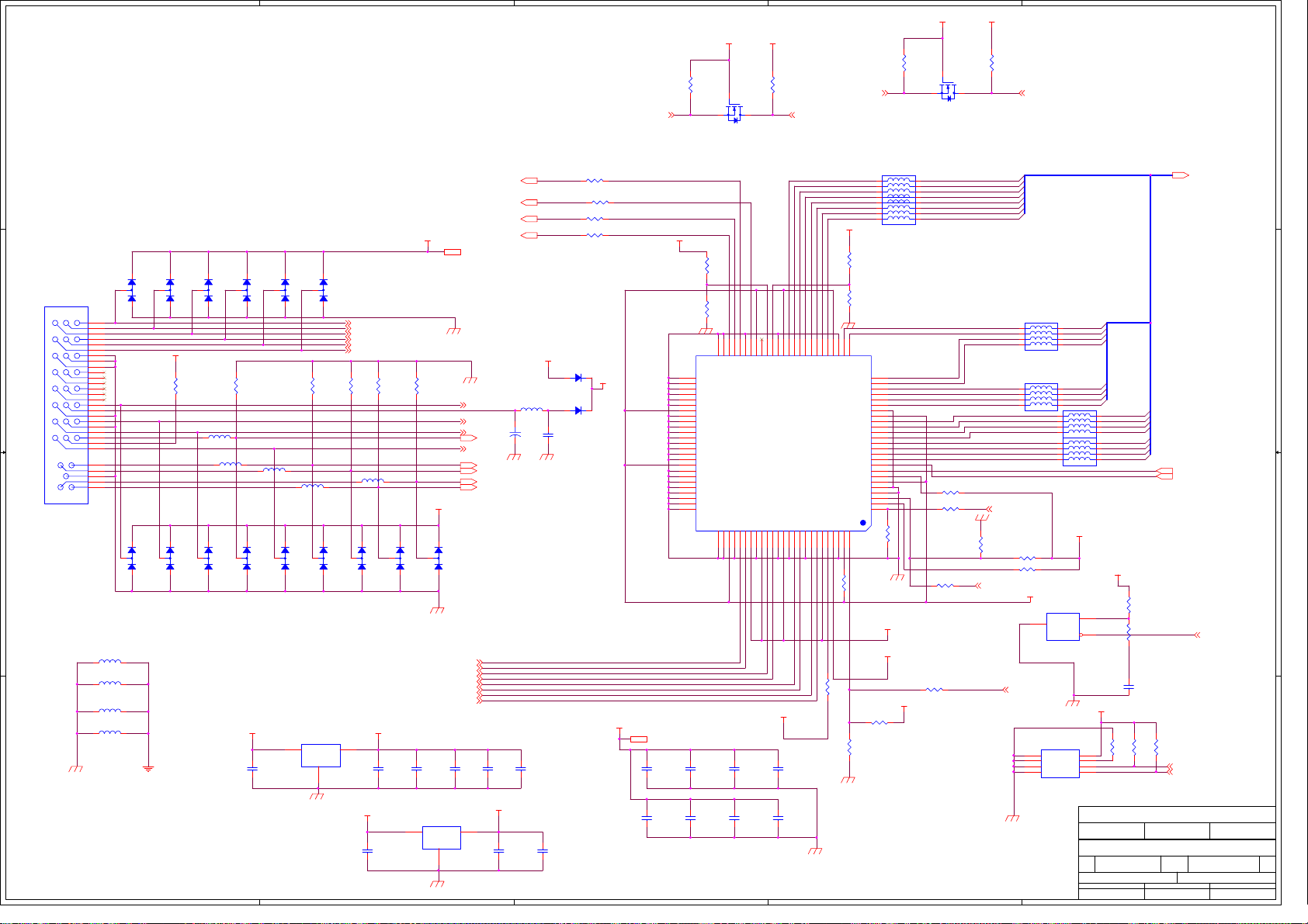
5
D D
2
D22
3
3
J10
1
9
17
2021008024
2
10
18
3
11
19
4
12
20
5
13
21
6
14
22
7
15
23
8
16
24
C1
C3
C5
C4
C2
C C
B B
A A
BAV99
1
PC_5V PC_5VIN
HOT_PLUG
2
D28
3
3
BAV99
1
L45
42 OHM
L44
42 OHM
L43
42 OHM
L42
42 OHM
5
2
D23
BAV99
1
+5V_EDID
51K
2
D29
BAV99
1
R79
PC_V
PC_R
PC_B
PC_H
PC_G
2
D24
3
3
BAV99
1
L28
42 OHM
42 OHM
L29
2
D30
3
3
BAV99
1
2
2
D25
3
BAV99
1
R80
4.7K
42 OHM
L33
2
D31
3
BAV99
1
+5V_AD +3V_ADVI
C157
4.7U Z
D26
BAV99
1
2
D32
BAV99
1
3
LD1117-3.3V
2
D27
3
BAV99
1
R81
75
L31
42 OHM
2
D33
3
BAV99
1
U19
VOUT
VIN
GND
1
4
+5V_AD
(open)
1 2
1 2
C175
0.1U Z
D38
1N4148
D37
1N4148
R1
R87
R2
R3
DVI_ACTDATA
DVI_CLK
D_VSYNC
D36
BAV99
+5V_AD
DVI_SCL
DVI_SDA
IDCK+
IDCK-
IDCK+
IDCK-
PC_RED
PC_BLUE
PC_HS
PC_GREEN
D2+
D2D1+
D1D0+
D0-
PC_VS
D_HSYNC
L34
42 OHM
12
+
C174
10U
16V
+5V_AD
D2D1D0D2+
D1+
D0+
R82
75
L32
2
D34
3
BAV99
1
R83
75
42 OHM
3
R84
4.7K
+5V_AD
2
2
D35
3
BAV99
1
1
2
C161
C160
+5V_AD
C163
4.7U Z
C158
4.7U Z
4
C159
0.1U Z
U20
3
VIN
LD1117-3.3V
0.1U Z
2
VOUT
GND
1
0.1U Z
+3V_PDVI
C164
4.7U Z
C162
0.1U Z
C165
0.1U Z
0
33
0
0
+5V_EDID
+3VD
3
DVI_SDA
+3VD
3
C166
0.1U Z
C170
0.1U Z
+5V_AD +3VD
R120
4.7K
1
3
2
Q4
BSN20
+3VD
R105
(open)
R106
(open)
51
52
53
54
55
56
57
58
59
60
61
62
63
64
65
66
67
68
69
70
71
72
73
74
75
0
0
QO2
QO3
QO4
QO5
QO6
QO7
OVCC
OGND
QO8
QO9
QO10
QO11
QO12
QO13
QO14
QO15
VCC
GND
QO16
QO17
QO18
QO19
QO20
QO21
QO22
DVIICLK
48
44
50
45
42
47
46
DE
QO049QO1
OVCC43ODCK
OGND
VSYNC
HSYNC
OGND76QO2377OVCC78AGND79RX2+80RX2-81AVCC82AGND83AVCC84RX1+85RX1-86AGND87AVCC88AGND89RX0+90RX0-91AGND92RXC+93RXC-94AVCC95EXT_RES96PVCC97PGND98RSVD99OCK_I
C168
C167
0.1U Z
0.1U Z
C172
C171
0.1U Z
0.1U Z
CTL2
CTL1
CTL140CTL241CTL3
SII151B
R121
4.7K
39
U17
+3VD
GND
DVI_RED7
38
37
VCC
C169
0.1U Z
C173
0.1U Z
DVI_SDA3V
DVI_RED6
DVI_RED4
DVI_RED5
DVI_RED2
DVI_RED3
R78
390
DVI_RED0
DVI_RED1
QE1630QE1731QE1832QE1933QE2034QE2135QE2236QE23
E_RES
29
28
OVCC
OGND
STAG_OUT
+3VD
27
RSVED
R103
(open)
R104
(open)
QE1426QE15
QE13
QE12
QE11
QE10
OGND
OVCC
SCDT
HS-DJTR
100
R96
10K
OCLK_INV
R77
10K
DVI_SCL
0
0
QE9
QE8
QE7
QE6
QE5
QE4
QE3
QE2
QE1
QE0
PDO
VCC
GND
PIXS
ST
PD
(open)
LP7
6
7
8
6
7
8
LP8 120 OHM
25
24
23
22
21
20
19
18
17
16
15
14
13
12
11
10
9
8
7
6
5
4
3
2
1
R100
0
+3V_ADVI
+3V_PDVI
R76
1.5K
2
120 OHM
SG_OUT
+3VD
2
R122
4.7K
45
3
2
1
45
3
2
1
HS_DJTR
R99
2
(open)
0
+5V_AD +3VD
1
3
Q5
BSN20
DVI_GREEN7
DVI_GREEN6
DVI_GREEN5
DVI_GREEN4
DVI_GREEN3
DVI_GREEN2
DVI_GREEN1
DVI_GREEN0
10K
R98
0
R101
(open)
ST
PD
0
R102
DVI_SDA3V
(OPEN)
R123
4.7K
D_INA23
D_INA22
D_INA21
D_INA20
D_INA19
D_INA18
D_INA17
D_INA16
RESETZ_DVI
R75
NC_R0603
(open)
6
7
8
6
7
8
DVI_BLUE7
DVI_BLUE6
DVI_BLUE5
DVI_BLUE4
DVI_BLUE3
DVI_BLUE2
DVI_BLUE1
DVI_BLUE0
R85
R86
DVI_SCL3V
DVI_SCL3V
LP9 120 OHM
LP10 120 OHM
1.5K
1.5K
+3VD
U21
2
GND
AME8500BEETAF29
U18
1
NC
2
NC
3
NC
GND4SDA
AT24C16 16K
1
D_INA[0..23]
D_INA15
45
D_INA14
3
D_INA13
2
D_INA12
1
D_INA11
45
D_INA10
3
D_INA9
2
D_INA8
1
LP11 120 OHM
6
7
8
6
7
8
LP12 120 OHM
+3VD
VDD
RES
VCC
WP
SCL
D_INA7
45
D_INA6
3
D_INA5
2
D_INA4
1
D_INA3
45
D_INA2
3
D_INA1
2
D_INA0
1
+3VD
EDID_VCC
3
1
+5V_EDID
R107
1K
8
WP
7
6
5
Benq Corporation
Project Code
99.J5877.001
Title
Size Document Number Rev.
PCB P/N
<Size>
48.J5810.S02
Monday, February 17, 2003
Date: Sheet
Prepared By
ANGEL HU
DVI_SCDT
DVI_PDO
R110
180
R111
100K
RESETR111
C176
1U Z
R108
R109
4.7K
4.7K
DVI_SCL
DVI_SDA
Model Name
HT720G
CONNECTOR BOARD
PCB Rev.
S02
Reviewed By Approved By
ALEX HY TSENG BEN CHEN
1
RESETZ_DVI
OEM/ODM Model Name
99.J5877.R22-C3-304-004
NA
0
of
88
 Loading...