

Page 1
H
10 (Data-Only)
Datasheet
HSDPA PCI Expre
Datasheet
Rev. 0.2 (Preliminary)
2007/06/22
ss
mini card
module
COPYRIGHT BENQ Corporation
This document contains proprietary technical information which is the property of BenQ Corporatio
and is issued in strict confidential and shall not be disclosed to others parties in
without written permission of BenQ Corporation
The documents contain information on a product, which is under development and is issued for
customer evaluation purposes only.
BENQ may make changes to product specifications at any time, without notice.
whole or in parts
n
1
Page 2
BenQ Corporatio
Mobile Co
18 JiHu Road, Nei-Hu, Taipei 114, Taiwan, R.O.C.
mmunications BG
n
Tel: +886-2-2799-8800
Fax: +886-2-2656-6390
http://
www.BenQ.com
HISTORY
Version
VER: 0.
VER: 0.
1
2
Dat
e
2007-APR-24
2007-JUN-22
FIRST RELEASE
Update characteristic of R
F
Notes
2
Page 3

1. INTRODUCTIO
1.1 Description
N
.....................................................................................................
.........................................................................................................4
4
1.2 Application Device
2. FEATURES
...............................................................................................................
2.1 General Characteristics
2.2 RF Functionalities
Maximum TX Power
Parametric Performance
Sensitivity
.........................................................................................................7
Radio Frequency
3. HARDWARE DESCRIPTION
3.1 System Interface
3.2 Functional Diagram
3.3 Pin Descriptio
3.4 Terminal Definition
3.5 Electrical Characteristics
DC characteristic
..............................................................................................4
.......................................................................................5
...............................................................................................6
........................................................................................6
................................................................................... 6
...............................................................................................7
.....................................................................................
..................................................................................................9
.......................................................................................... 10
n
................................................................................................. 11
.......................................................................................... 13
................................................................................... 15
s
........................................................................................... 15
5
9
Digital interface
USB Transceiver DC characteristic
USIM Interface
3.6 Environmenta
3.7 Physical Package
4. SOFTWARE CHARACTERISTIC
4.1 Introduction
4.2 Software Architectur
.............................................................................................. 16
s
................................................................. 16
............................................................................................... 17
l
.................................................................................................. 17
............................................................................................... 18
S
............................................................................
..................................................................................................... 21
e
........................................................................................ 21
21
5.1 Compliance with FCC Rules and Regulations
3
Page 4

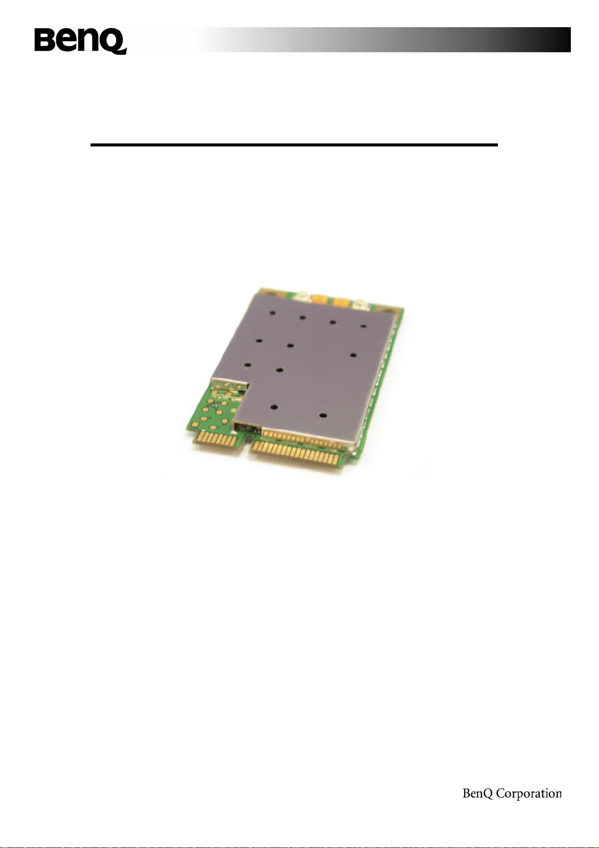
1. INTRODUCTIO
N
1.1 Descrip便ion
Overview
This document describes all the functions, features, and interfaces of the HSDP
PCI Express Mini Card Module -- H10 from BenQ. BenQ H10
HSDPA module su
pports Tri-band WCDMA/HSDPA and Quad-band
A
GSM/GPRS/EDGE network connection capability.
BenQ H10 HSDPA card can provides high speed data connection, and the
data speed of downlink path is up to
7.2Mbps. Furthermore, users can
ease to use this module by using the “Qsyncher” application software that we
provide for Windows XP and Vista system.
With the BENQ H10 HSDPA module, devices are enhanced in both functionalit
and usability based on state of the art wireless technology.
y
1.2 Applica便ion Device
Scope
BenQ H10 module is a high speed modem card with PCI Express minicard for
m
factor and is focusing on the Notebook, UMPC, MID and other
portable device marketing.
汗 No便ebook
汗 Ul便ra Mobile PC
汗 Mobile In便erne便 Device
汗 Wireless Rou便er
汗 USB Modem
汗 Car Embedded Sys便e
m
4
Page 5
2. FEATURE
S
2.1 General Charac便eris便ics
BAND
GSM
Ban
d
GSM
850
EGSM900
DCS
1800
PCS
1900
WCDMA
WCDMA
WCDMA
Su
:
850/EGSM900/DCS
850
1900
2100
pport SIM Interface:
T
X
824~849 MH
880~915 MH
1710~1785MHz
1850~1910MHz
824~849 MH
1850~1910MHz
1920~1980MHz
1.8V/3V
1800/PCS
z
z
z
1900/WCDMA
850/WCDMA
R
X
869~894MHz
925~960MHz
1805~1880MHz
1930~1990MHz
869~894MHz
1930~1990MHz
2110~2170MHz
1900/WCDMA
2100
Form factor
i.
Dimension:
ii.
Weight: 12g
Power
Operation Voltage:
Power Consumption:
50.95 x 30 x 5.0 mm
3.3V +/- 9%
Speech Mode:
Ban
d
GSM
850 / PCL=5
EGSM900 / PCL=5
DCS / PCL=0
PCS / PCL=0
WCDMA (all band)
Typ
385
395
312
280
720
M
a
x
400
mA
410
mA
325
mA
295
mA
820
mA
Uni
t
Standby Mode:
GSM / Page frame=2
Typ (Average)
3.5
Max (Average
4.5
mA
)
Uni
t
GSM / Page frame=9
DCS / Page frame=2
DCS / Page frame=9
PCS / Page frame=2
PCS / Page frame=9
WCDMA / DRX=6 (0.64 S)
WCDMA / DRX=9 (5.12 S)
2.0
3.5
2.0
3.5
2.0
3.6
1.5
5
3
mA
4.5
mA
3
mA
4.5
mA
3
mA
4.5
mA
3
mA
Page 6
Hardware Interface:
52 Pins PCI Express Mini Card connector interface
2 RF Antenna Coaxial Connectors
Software Interface
:
USB driver
Qsyncher software tool.
2.2 RF Func便ionali便ies
Maximum TX Power
The performance of the transmitter meets test requirement ETSI TS 151 010-1 chapter
13.3 for GSM, chapter
13.17.3 for EDGE and TS 34.121 chapter 5.2&5.4.3 for WCDMA
chapter 5.2A for HSDPA
Ban
d
GSM8S
0
EGS
M
DCS
PCS
GSM8S0(EDGE
EGSM(EDGE
DCS(EDGE)
PCS(EDGE)
UMTS-
UMTS-
UMTS-8S
1/1
S βo/βd 12/1S (HS-DPCCH
13/1
S βo/βd 1S/8 (HS-DPCCH
1S/
7 βo/βd 1S/0 (HS-DPCCH
2100
1900
)
)
0
)
)
)
M
a
x
33 dBm ±2dB
33 dBm ±2dB
30 dBm ±2dB
30 dBm ±2dB
27 dBm ±3dB
27 dBm ±3dB
26 dBm ±3dB
26 dBm ±3dB
24 dBm +1/-3d
24 dBm +1/-3d
24 dBm +1/-3d
24 dBm +1/-3d
23 dBm +2/-3d
22 dBm +3/-3d
m
m
m
m
m
m
m
m
B
B
B
B
B
B
m
m
m
m
m
m
Min
S dBm ±SdB
S dBm ±SdB
0 dBm ±SdB
0 dBm ±SdB
S dBm ±SdB
S dBm ±SdB
2 dBm ±SdB
2 dBm ±SdB
Less than -S0d
Less than -S0d
Less than -S0d
m
m
m
m
m
m
m
m
B
m
B
m
B
m
Parame便ric Performanc
e
,
Tests carried out at -20ºC, 25ºC and 60ºC for each voltage 3V,
3.3V and
3.6V. The Measured Peak Phase, RMS Phase, frequency error, power level,
and static sensitivity meets ETSI TS
151 010-1 chapter 13.1 for GSM and TS
34.121
chapter 5.13.1 for WCDMA, chapter 5.13.1A for HSDPA
Band (GSM
GSM8S
EGS
M
DCS
PCS
Band (WCDMA
UMTS-
UMTS-
UMTS-8S0(HS-DPCCH)
)
0
)
2100(HS-DPCCH
1900(HS-DPCCH
Peak Phase Erro
<
20°
<
20°
<
20°
<
20°
)
)
Error Vector Magnitude
<17.S%
<17.S%
<17.S%
r
RMS Phase Erro
<S°
<S°
<S°
<S°
r
6
Page 7
Sensi便ivi便y
The performance of the receiver meets test requirement ETSI TS
for GSM, chapter
14.18.1 for EDGE and TS 34.121 chapter 6.2 for WCDMA.
151 010-1 chapter 14.2.1
Ban
d
GSM8S
0
EGS
M
DCS
PCS
EDGE(GMSK modulation)
EDGE(8-PSK modulation
UMTS-
2100(Primary
UMTS-
2100(Secondary
UMTS-
1900
UMTS-8S0(Primary)
UMTS-8S0(Secondary)
Radio Frequency
GSM
850 (
850 MHz)
Frequency Range
Channel Spacin
Number of Channel
Modulation
Duplex Spacing
Frequency Stability
Power Output
Output Impedanc
Spurious Emissio
EGSM (900 MHz)
Frequency Range
Channel Spacin
Number of Channel
Modulation
Duplex Spacing
Frequency Stability
Power Output
Output Impedanc
Spurious Emissio
DCS (
Frequency Range
Channel Spacin
Number of Channel
Modulation
Duplex Spacing
Frequency Stability
Power Output
g
e
n
g
e
n
1800 MHz)
g
)
)
)
TX
824-849 MHz; RX
200 KHz
s
124 Carriers x 8 (TDMA)
GMSK / 8-PS
4S MHz
+/- 0.1 ppm (Uplink TX)
33 dBm Class 8 (2 W peak) – S d
S0 O
h
m
-36 dBm up to 1 GHz (< -30 dBm > 1 GHz)
TX
880-91S MHz; RX 92S-
200 KHz
s
124 Carriers x 8 (TDMA)
GMSK / 8-PS
4S MHz
+/- 0.1 ppm (Uplink TX)
33 dBm Class 8 (2 W peak) – S d
S0 O
h
m
-36 dBm up to 1 GHz (< -30 dBm > 1 GHz)
TX
1710-178S MHz; RX 180S-
200 KHz
s
374 Carriers x 8 (TDMA)
GMSK / 8-PS
9S MHz
+/- 0.1 ppm (Uplink TX)
30 dBm – 0 dB
K
K
K
869-894 MH
m
960 MH
Typical
-
107 d
-
107 d
-
107 d
-
107 d
-
107 d
-
104 d
-
109 d
-
109 d
-
107 d
-
109 d
-
109 d
z
B
m
z
B
m
1880 MH
B
m
B
m
B
m
B
m
B
m
B
m
B
m
B
m
B
m
B
m
B
m
Min
-
104 d
-
104 d
-
103 d
-
103 d
-
104 d
-
102 d
-
106.7 d
-
104.7 d
-
106.7 d
N/A
N/A
B
m
B
m
B
m
B
m
B
m
B
m
B
m
B
m
B
m
z
7
Page 8

Output Impedanc
Spurious Emissio
PCS (
1900 MHz)
Frequency Range
Channel Spacin
Number of Channel
Modulation
Duplex Spacing
Frequency Stability
Power Output
Output Impedanc
Spurious Emissio
e
n
g
e
n
WCDMA_IMT (
Frequency Range
Channel Raster
Number of Channel
Modulation
Duplex Spacing
Frequency Stability
Power Output
Output Impedanc
Spurious Emissio
Q
e
n
WCDMA_PCS (
Frequency Range
Channel Raster
Number of Channel
Modulation
Duplex Spacing
Frequency Stability
Power Output
Output Impedanc
Spurious Emissio
Q
e
n
WCDMA_850 (
Frequency Range
Channel Raster
Number of Channel
Modulation
Duplex Spacing
Frequency Stability
Power Output
Output Impedanc
Spurious Emissio
Q
e
n
s
2100 MHz)
s
1900 MHz)
s
850 MHz)
s
S0 O
h
m
-36 dBm up to 1 GHz (< -30 dBm > 1 GHz)
Compatible with phase 2 featur
TX: 18S0~1910MHz; RX:
200KH
z
299 Carriers x 8 (TDMA)
GMSK / 8-PS
80 MH
+/- 0.1 ppm (Uplink TX)
30 dBm – 0 dB
S0 O
-36 dBm up to 1 GHz (< -30 dBm > 1 GHz)
Compatible with phase 2 featur
K
z
m
h
m
e
1930~1990MHz
e
TX: 1920~1980MHz; RX:
200KH
z
299 Carriers x 8 (TDMA)
PSK
190 MH
z
+/- 0.1 ppm (Uplink TX)
24 dBm +1/-3dBm - less than -S0dB
S0 O
h
m
-67dBm(92S-93SMHz);-79dBm(93S-960MHz);-71dBm(
;-60dBm(
184S-
1880MHz);-41dBm(
2110~2170MHz
m
188S-
1920MHz
180S-
)
1880MHz)
TX: 18S0~1910MHz; RX:
200KH
z
299 Carriers x 8 (TDMA)
PSK
80 MH
z
+/- 0.1 ppm (Uplink TX)
24 dBm +1/-3dBm - less than -S0dB
S0 O
h
m
1930~1990MHz
m
TX
824-849 MHz; RX
200KH
z
299 Carriers x 8 (TDMA)
PSK
4S MHz
+/- 0.1 ppm (Uplink TX)
24 dBm +1/-3dBm - less than -S0dB
S0 O
h
m
-60dBm(869-894MHz;1930-1990MHz;2110-21SSMHz)
869-894 MH
z
m
8
Page 9

3. HARDWARE DESCRIPTION
3.1 Sys便em In便erface
The I/O connectors of H10 module are PCI EXPRESS MINI CARD and two RF antenna
connectors. Table 3-1 su
mmarizes the 25 signals and 18 power lines that are su
pported by
the PCI Express Mini Card System Interface. Table 3-2 shows the antenna interface.
Table 3-1 System Interface
Signal Grou
Power
G
ND
USB
PERST#
W_DISABLE
UIM
LED
p
#
Pin no.
S
13
2
1
1
4
3
Descripti
3.3V power sourc
Return current pat
USB serial data interface compliant to the USB 2.0 specification
Function reset to the card
Shutdown the HSDPA module
SIM function
Status indicators
o
n
e
h
Signal Grou
ANT
p
Connector no.
Table 3-2 Antenna interface
2
A
Descripti
ntenna interface
o
n
9
Page 10

3.2 Func便ional Diagra
m
1
Page 11

3.3 Pin Descrip便ion
Pin
Signal name
Direction
Description
1 N
2 +3.3Vau
3 N
4 G
5 N
6 N
7 N
8 UIM_PWR
9 G
10 UIM_DAT
11 N
12 UIM_CLK
13 N
14 UIM_RESET
15 G
16 N
C
C
ND
C
C
C
ND
C
C
ND
C
x
A
Power
Power
Outpu
t
Power
Input / Outpu
Outpu
t
Outpu
Power
t
No connect
3.3V power sourc
No connect
Return current pat
No connect
No connect
No connect
Power source for the USIM
Return current pat
t
USIM data signa
No connect
USIM clock signal
No connect
USIM reset signal
Return current pat
No connect
e
h
h
l
h
17 N
18 G
19 N
20
21 G
22
23 N
24 +3.3Vau
25 N
26 G
27 G
28 N
29 G
C
ND
C
W_DISABLE
ND
PERST#
C
C
ND
ND
C
ND
x
Power
#
Input
Power
Input
Power
Power
Power
Power
No connect
Return current pat
No connect
Active low signal.
This signal is used by the system t
shutdown the HSDPA module.
Return current pat
Active low signal.
Function reset to the card
No connect
3.3V power sourc
No connect
Return current pat
Return current pat
No connect
Return current pat
h
h
.
e
h
h
h
o
30 N
31 N
C
C
1
No connect
No connect
Page 12

32 N
C
No connect
33 N
34 G
35 G
36 USB_D
37 G
38 USB_D
39 +3.3Vau
40 G
41 +3.3Vau
42
43 G
44
45 N
46
C
ND
ND
-
ND
+
x
ND
x
LED_WWAN
ND
LED_WLAN#
C
LED_WPAN#
Power
Power
Input / Outpu
Power
Input / Outpu
Power
Power
Power
#
Outpu
Power
Outpu
t
t
Outpu
t
No connect
Return current pat
Return current pat
t
USB serial data interface (negative
Return current pat
t
USB serial data interface (postive
3.3V power sourc
Return current pat
3.3V power sourc
Active low signal.
WAN status LED driver
Return current pat
Active low signal.
LAN status LED driver
No connect
Active low signal.
PAN status LED driver
h
h
h
e
h
e
h
)
)
.
.
.
47 N
48 N
49 N
50 G
51 N
52 +3.3Vau
C
C
C
ND
C
Power
x
Power
No connect
No connect
No connect
Return current pat
No connect
3.3V power sourc
h
e
1
Page 13

3.4 Terminal Defini便ion
Recommend an便enna connec便
Hirose Coaxial Connectors
1
Page 14

Sys便em connec便o
r
52 pins PCI Express Mini Card
1
Page 15

3.5 Elec便rical Charac便eris便ic
DC charac便eris便ics
Pin
1 N
Function/ Name
C
Direction
s
Parameter
Min Typ M
ax Uni
t
2 +3.3Vau
3 N
C
4 G
ND
S N
C
6 N
C
7 N
C
8
UIM_PWR
9 G
ND
10 UIM_DAT
11
NC
12
UIM_C
13 N
C
14 UIM_RESE
1
S G
ND
16 N
C
x
A
LK
T
O
Power
Power Supply Voltage
3.0 3.3 3.6
Power
Ground
Outpu
t
Power
Input / Output
Supply Voltage
Curren
Ground
t
1.S 2.8
S 3.0
1S0
Outpu
t
utput
Power
Ground
S V
m
V
A
17 N
18 G
19 N
20
W_DISABLE
21 G
22
PERST#
23 N
24 +3.3Vau
2
S N
26 G
27 G
28 N
29 G
30 N
31 N
C
ND
C
ND
C
C
ND
ND
C
ND
C
C
#
x
Power
Input
Power
Input
Power
Power
Power
Ground
Logic High Input Voltag
Logic Low Input Voltage
Ground
Logic High Input Voltag
Logic Low Input Voltage
Power Supply Voltage
Ground
Ground
e
1.69 2.6 2.9
-0.
3 0 0.91 V
e
1.69 2.6 2.9
-0.
3 0 0.91 V
3.0 3.3 3.6
Power
Ground
V
V
V
1
Page 16

32 N
33
34
3
S G
NC
G
C
ND
ND
Power
Power
Ground
Ground
36 USB_D-
37 G
38 USB_D+
39 +3.3Vau
40 G
41 +3.3Vau
42 LED_WWAN
43 G
44 LED_WLAN#
4
S N
46 LED_WPAN#
47 N
48 N
49 N
S
0 G
S
1 N
ND
ND
ND
C
C
C
C
ND
C
x
x
#
O
O
O
Input / Output
Power
Input / Output
Power
Power
Power
utput
Power
utput
Termination Voltage
Ground
Termination Voltage
Power Supply Voltage
Ground
Power Supply Voltage
Driver current
Ground
Driver current
3.0 3.3 3.6
3.0 3.3 3.6
3.0 3.3 3.6
3.0 3.3 3.6
0
1S0
0
1S0
utput
Driver current
0
300
Power
Ground
m
m
m
V
V
V
V
A
A
A
S
2 +3.3Vau
x
Power
Power Supply Voltage
3.0 3.3 3.6
V
Digi便al in便erface
Logic High Input Voltag
Logic Low Input Voltage
Logic High Output Voltag
Logic Low Output Voltage
Parameter
e
e
Min
1.69
-0.
2.1
-0.
3
S
3
Typ
2.6
0
2.6
0
M
0.91
0.4
2.9
2.6
a
x
S
Uni
t
V
V
V
V
USB Transceiver DC charac便eris便ic
The USB interface is powered from
Parameter
Input sensitivity (differential)
Output voltage
Logic LOW
Logic HIG
Comments
|D+ D-|,
RL=1.SKΩ to 3.6V
H
RL=1.SKΩ to GND, IO=1m
s
3.3V power source.
V
=0.8 to 2.S
I
N
V
A
Min
Typ
M
a
x
Uni
t
0.2
2.8
0.3
3.6
V
V
V
Series output resistanc
e
D+, D
-
28
33
44
Ω
1
Page 17

Internal pull-up resisto
r
3.3V to D+, 3.3V to D
-
1.42
S
1.S
1.S7S
K
Ω
Internal pull-down resistor
USIM In便erfac
The USIM signals are defined on system connector to provide the interface between th
removable User Identity Module. USIM interface usually run off either
Pin
8
UIM_PWR
10
UIM_DAT
12
UIM_C
14
UIM_RESE
Parameter
Logic High Input Voltag
Logic Low Input Voltage
Logic High Output Voltag
Logic Low Output Voltage
e
Nam
e
O
A
LK
O
T
O
e
e
D+ to GND, D- to G
Direction
utput
Input / Output
utput
utput
Comments
ND
14.3
1
S
24.8
K
Ω
e
1.8V or 3.0V.
Description
Power source for the USIM
USIM data signa
USIM clock signal
USIM reset signal
Min
1.8S2
-0.
2.4
-0.
l
Typ
S
2.8
3
2.8
3
M
S
3.1
0
0.997
S
2.8
0
0.4
a
x
Uni
t
S
S
S
S
V
V
V
V
Schmitt Hysteresis
Logic input leakage current
Internal pull-up resisto
3.6 Environmen便al
Operational temperature: -20 ~ +60
Functional temperature: -20 ~ +70
Storage temperature: -40 ~ +85
r
Programmable range
1S0
-
200
1
200
30
m
V
n
A
K
Ω
1
Page 18

3.7 Physical Packag
Top View
e
1
Page 19

Bo便便om View
1
Page 20

Side View
2
Page 21

4. SOFTWARE CHARACTERISTICS
4.1 In便roduc便ion
We provide the PC Tool – Qsyncher for H10 HSDPA card. The main functions in this
tool are Contacts (only SIM card), SMS, Settings, and QMI.
QMI is the independent network software; user can run this service alone without
Qsycher active.
4.2 Sof便ware Archi便ec便ure
2
Page 22

5
Compliance with FCC Rules and Regulations
15.21
Federal
You a
re
sponsib
15.105(b)
Fe
This equipment has been tested and
Communications Commission (FCC) Statement
re c
autioned that changes or modifications not expressly approved by the part
le for c
omplian
ce could void the user’s
authority to operate th
deral Communications Commission (FCC) Statement
found to comply with th
e limits
e equipme
for
a Class B digital
nt.
dev
ice,
designed
a residential installati
frequency energy and, if no
instructi
However,
par
ticular installati
to radio
off and on, the user
or
more of the followi
-Reorient or relo
-Increas
-Conn
t
o which
-Consu
pursuan
to
ons,
t to part 15 of the FCC rules. These limits are
provide reasonab
on.
le
pro
tection against harmful interference in
This equipment generates, uses and can radiate radio
t installed a
nd used
in acc
ordan
ce with the
may cause harmful interference to radio communicati
there is no guarantee that interference will not occur in a
on. If
or
television recepti
is enc
this equipment does cause harmful interference
ouraged
ng
mea
on, which
sures
can be determined by t
to try to c
orr
ect the interference by one
:
urning th
e equipment
cate the receiving antenna.
e the separation between the equipment and receiver.
ect the equipment into an outlet on a circuit different
the receiver is c
lt the dealer or an experienced radio/TV technician
onn
ected.
for help.
fro
m that
ons.
You
are cautioned that changes or modificati
ons no
t e
xpressly
a
pproved by
t
h
e part
oper
Operation is
1) this dev
2) this dev
undesired oper
y responsib
ate the equipment.
subject to the following two conditions:
ice may not cause interference and
ice must accept any interference, including interference that may cause
ation of the device.
le
for
compliance could void
2
your
aut
hority
to
Page 23

FCC RF
1.
This Transmitter must not be co-located or operating in conjunction with any
Radiation Exposu
re
Statement:
other antenna or trans
mitter.
This equipment complies with FCC RF radiation e
uncontro
lled envi
ronment. This equipment should b
minimum distance of 20 centimeters between the radiator and
OEMs who install this module into an enclosure where the module’s FCC ID label is not
visible from the outside of the enclosure must label the enclosure with these words:
‘Contains Transmitter Module FCC ID: JVPH10.’ Failure to follow these labeling instructions
makes the OEM subject to sanctions from the FCC.”
xposur
e limits set
forth for an
e installed and operated with a
your body.
2
 Loading...