

Page 1

Q7T4-FP71G LCD Monitor Service Guide
Alignment Procedure
1. Alignment procedure (for function adjustment)
A. Preparation:
1. Setup input timing ICL-605( 1280x1024@75Hz ), 32-Grays pattern.
2. Setup unit and keep it warm up at least 30 minutes.
B. Timing adjustment:
1. Enter factory setting area (press “ENTER”, “EXIT” and then press “SOFTPOWER”).
2. Check the settings to following values:
Then, turn off the monitor power.
3. Turn on power enter user area.
C. Color balance adjustment:
Contrast = 50
Brightness = 90
OSD time = 20
Color = Normal
Language = English
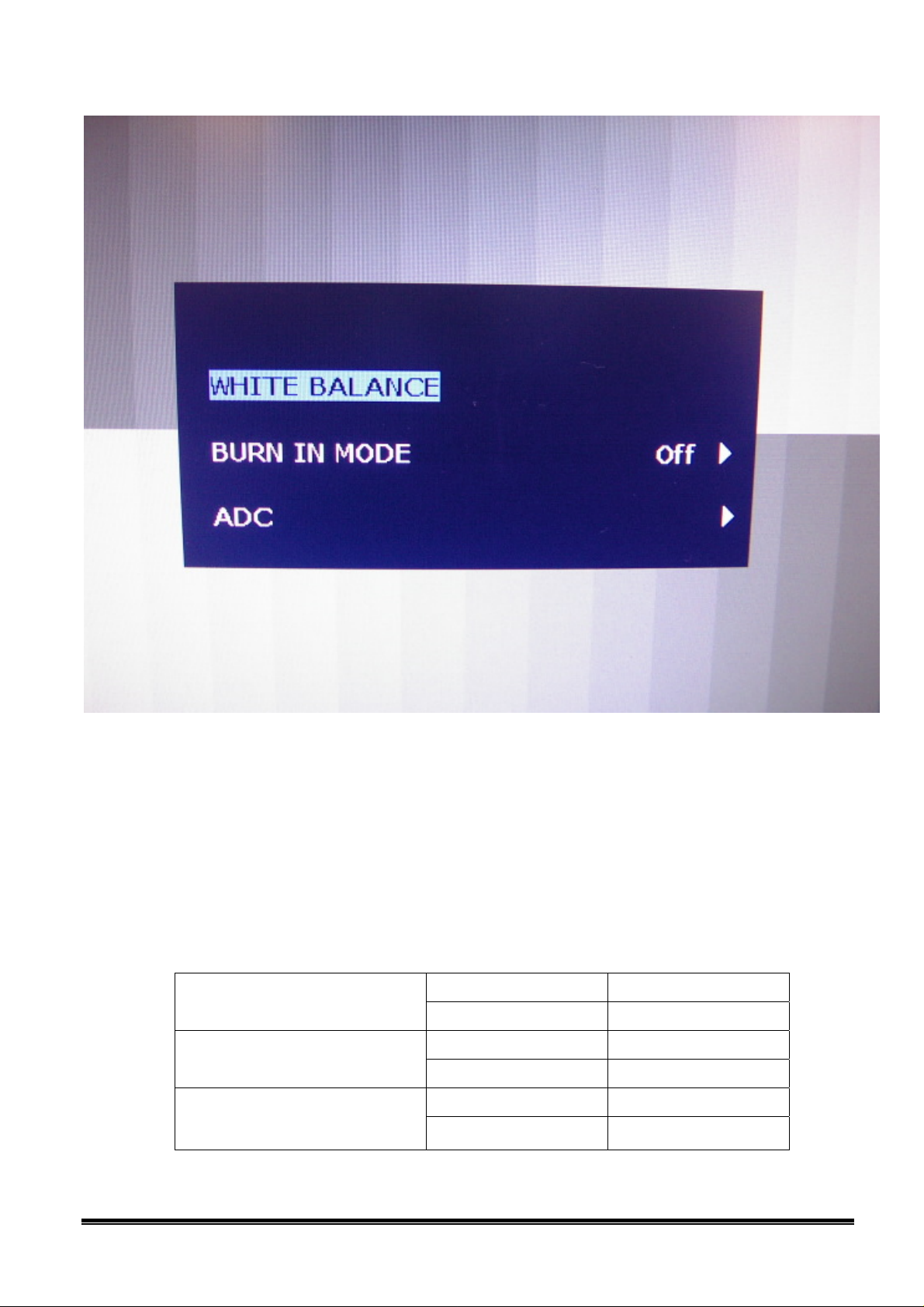
1. Enter factory setting area (press “ENTER”, “I-Key” and then press “SOFTPOWER”).
2. Setup input timing ICL-605(1280x1024@75Hz), 32-Gray pattern (pattern 48) .
3. Press “I-KEY”, and than OSD will show “White Balance” item and than press “ENTER” button
to do auto color.
1
Confidential
Page 2
Q7T4-FP71G LCD Monitor Service Guide
Alignment Procedure
D. Color adjustment:
1. Setup input timing ICL-605, white pattern .
2. Confirm auto color adjustment had already done.
3. Measure color temperature by Minolta CA-110 (or equivalent equipment).
4. Check the color temperature Bluish, Reddish & Normal. The color temperature specification
as follows:
X+- 0.283+(-) 0.03 White Balance
(Bluish, 9300K set on OSD)
Y+- 0.297+(-) 0.03
X+- 0. 326+(-) 0.03 White Balance
(Reddish, 5800K set on OSD)
Y+- 0. 342+(-) 0.03
X+- 0.313+(-) 0.03 White Balance
(sRGB, 6500K set on OSD)
Y+- 0. 329 +(-) 0.03
2
Confidential
Page 3
Q7T4-FP71G LCD Monitor Service Guide
Alignment Procedure
5. Setup input timing , 32 -Gray pattern.
To check if there are any abnormal display problems of preset timing modes .
Check the following preset timings with General pattern:
No. Mode H V
1 720×400 @ 70Hz 31.468 70.8
2 640×480 @ 60Hz 31.469 59.940
3 640×480 @ 75Hz 37.500 75.000
4 800×600 @ 60Hz 37.879 60.317
5 800×600 @ 75Hz 46.875 75.000
6 1024×768 @ 60Hz 48.363 60.004
7 1024×768 @ 75Hz 60.023 75.029
8 1152x864 @ 75Hz 67.500 75.000
9 1280×1024 @ 60Hz 63.981 60.020
10 1280×1024 @ 75Hz 79.976 75.025
6. Checking if the picture is no good, reject this monitor.
7. To check the power consumption by disabling “burn-in mode” setting
8. To clear user data and program complete DDC data to monitor by IIC bus communication.
E. Writing EDID file:
1. Setup a PC with DDC card.
2. Connect PC to monitor with a D-sub signal cable.
3. Please refer to the C212 for the correct EDID file.
4. Runs the writing program to write the EDID file into EEPROM .
5. Read EEPROM data and confirm it to match with the C212 document definition.
F. Command definition :
PC Host will send 0x7C IIC slave address and then following 4 bytes command
I2C Send Command
Write Contrast to MCU RAM CA 55 Data cksum
Write Brightness to MCU RAM CA 56 Data cksum
Write Red Gain to MCU RAM CA 57 Data
Write Green Gain to MCU RAM CA 58 Data cksum
Write Blue Gain to MCU RAM CA 59 Data cksum
Read Contrast from MCU RAM C3 55 XX cksum
Read Brightness from MCU RAM C3 56 XX cksum
Read Red Gain from MCU RAM by color index C3 57 XX cksum
Read Green Gain from MCU RAM by color
index C3 58 XX cksum
Read Blue Gain from MCU RAM by color index C3 59 XX cksum
Write C1 (Bluish) R-Gain Data to EEPROM AA 3C Data cksum
Write C1 (Bluish) G-Gain Data to EEPROM AA 3D Data cksum
Write C1 (Bluish) B-Gain Data to EEPROM AA 3E Data cksum
Write C2 (sRGB) R-Gain Data to EEPROM AA 4C Data cksum
Write C2 (sRGB) G-Gain Data to EEPROM AA 4D Data cksum
Write C2 (sRGB) B-Gain Data to EEPROM AA 4E Data cksum
Byte1 Byte2 Byte3
Byte4
cksum
OK N.A. Remark
√
√
√
√
√
√
√
√
√
√
√
√
√
√
√
√
Write data to MCU RAM and
update the related register to
refresh the screen immediately.
Don’t store data to EEPROM.
Base on current color index to
read back the right gain value.
3
Confidential
Page 4
Q7T4-FP71G LCD Monitor Service Guide
Write C3 (Reddish) R-Gain Data to EEPROM AA 5C Data cksum
Write C3 (Reddish) G-Gain Data to EEPROM AA 5D Data cksum
Write C3 (Reddish) B-Gain Data to EEPROM AA 5E Data cksum
Write User R-Gain Data to EEPROM AA 6C Data cksum
Write User G-Gain Data to EEPROM AA 6D Data cksum
Write User B-Gain Data to EEPROM AA 6E Data cksum
Write Cx R-Gain Data to EEPROM AA 7C Data cksum
Write Cx G-Gain Data to EEPROM AA 7D Data cksum
Write Cx B-Gain Data to EEPROM AA 7E Data cksum
Write Contrast to EEPROM AA 92 Data
Write Brightness to EEPROM
Write C/T index to EEPROM
Write OSD-Hpos to EEPROM
Write OSD-Vpos to EEPROM AA 96 Data
AA
AA
AA
93 Data
94 0~4
95 Data
cksum
cksum
cksum
cksum
cksum
√
√
√
√
√
√
√
√
√
√
√
Alignment Procedure
√
Reserved for some model have
√
extra color temperature
√
1=C1/9300/Bluish,
2=C2/6500/sRGB/,
3=C3/5800/Reddish,
4=User, 5=Cx
Write Language to EEPROM
Write EEPROM OSD Timer
Write EEPROM Volume
Write EEPROM Gamma index AA 9A Data
Write OSD Transparency to EEPROM
Write OSD Rotation to EEPROM AA 9F Data cksum
Read C1 (Bluish) R-Gain data from EEPROM A3 3C XX cksum
Read C1 (Bluish) G-Gain data from EEPROM A3 3D XX cksum
Read C1 (Bluish) B-Gain data from EEPROM A3 3E XX cksum
Read C2 (sRGB) R-Gain data from EEPROM A3 4C XX cksum
Read C2 (sRGB) G-Gain data from EEPROM A3 4D XX cksum
Read C2 (sRGB) B-Gain data from EEPROM A3 4E XX cksum
Read C3 (Reddish) R-Gain data from EEPROM A3 5C XX cksum
Read C3 (Reddish) G-Gain data from EEPROM A3 5D XX cksum
Read C3 (Reddish) B-Gain data from EEPROM A3 5E XX cksum
Read User R-Gain data from EEPROM A3 6C XX cksum
Read User G-Gain data from EEPROM A3 6D XX cksum
Read User B-Gain data from EEPROM A3 6E XX cksum
Read Cx R-Gain data from EEPROM A3 7C XX cksum
Read Cx G-Gain data from EEPROM A3 7D XX cksum
Read Cx B-Gain data from EEPROM A3 7E XX cksum
Read Contrast from EEPROM A3 92 XX
Read Brightness from EEPROM A3 93 XX
AA
AA
AA
AA
97 0~7
98 Data
99 Data
9E Data cksum
cksum
cksum
cksum
cksum
cksum
cksum
√
√
√
√
√
√
√
√
√
√
√
√
√
√
√
√
√
0=DE, 1=EN, 2=ES, 3=FR,
4=IT, 5=JA, 6=繁中, 7=簡中
(Also Update MCU RAM)
For model with Gamma curve
selection function
√
√
√
√
Reserved for some model have
√
extra color temperature
√
4
Confidential
Page 5
Q7T4-FP71G LCD Monitor Service Guide
And
Alignment Procedure
1=C1/9300/Bluish,
2=C2/6500/sRGB/,
3=C3/5800/Reddish,
4=User, 5=Cx
Read C/T index from EEPROM A3 94 XX
Read OSD-Hpos EEPROM A3 95 XX
Read OSD-Vpos from EEPROM A3 96 XX
Read Language from EEPROM A3 97 XX
Read OSD Timer from EEPROM A3 98 XX
Read Volume from EEPROM A3 99 XX
Read Gamma index from EEPROM A3 9A XX
Read OSD Transparency from EEPROM A3 9E XX cksum
Read OSD Rotation from EEPROM A3 9F XX cksum
Change Color Temp. to C1/9300K/Bluish CC 01 XX cksum
Change Color Temp. to C2/6500K/sRGB CC 02 XX cksum
Change Color Temp. to C3/5800K/Reddish CC 03 XX cksum
Change Color Temp. to User CC 04 XX cksum
Change Color Temp. to Cx CC 05 XX cksum
Change Input Source to D-Sub CD 01 XX cksum
Change Input Source to DVI CD 02 XX cksum
On burn in mode CE 01 XX cksum
Off burn in mode CE XX* XX cksum
Monitor is forced power saving CF 01 XX cksum
Monitor wake up from power saving CF XX* XX cksum
User mode to factory mode 1A 5A XX cksum
Auto Color (Offset1, Offset2, Gain) 1B 5A XX cksum
Copy EDID Serial number to EEPROM
Factory mode to User mode 1E 5A XX cksum
Clear user mode and factory recall 1F 5A XX cksum
Write EDID data to MCU DDC RAM
Copy DDC RAM data to EEPROM
Drive WP pin to low to enable write DDC IC
Drive WP pin to high to disenable write function
1C 5A XX cksum
55 NA NA NA
BB NA NA NA
55 NA NA NA
BB NA NA NA
cksum
cksum
cksum
cksum
cksum
cksum
cksum
EEPROM Bank R/W (For Debug using only, not for Production Line Write EEPROM directly)
Read EEPROM Bank 0 B0
Read EEPROM Bank 1 B1
Read EEPROM Bank 2 B2
Read EEPROM Bank 3 B3
Write EEPROM Bank 0 B8
Write EEPROM Bank 1 B9
Write EEPROM Bank 2 BA
Write EEPROM Bank 3 BB
Address
Address
Address
Address
Address
Address
Address
Address
XX cksum
XX cksum
XX cksum
XX cksum
Data cksum
Data cksum
Data cksum
Data cksum
√
√
√
0=DE, 1=EN, 2=ES, 3=FR,
4=IT, 5=JA, 6=繁中, 7=簡中
√
√
√
For model with Gamma curve
√
√
√
√
√
√
√
√
√
√
√
√
√
√
√
selection function
√
√
√
Change C/T immediately.
store C/T index to EEPROM.
Reserved
√
√
√
Store data to EEPROM
XX* = Non “1” value
Store data to EEPROM
√
XX* = Non “1” value
√
√
For specified “Industry
Customer” model.
√
Store data to EEPROM
For MTV312 MCU type
For MTV312 MCU type
For stand alone DDC IC
√
For stand alone DDC IC
√
(For 24C08 type)
√
(For 24C08 type)
√
(For 24C08 type)
√
(For 24C08 type)
√
5
Confidential
Page 6

Q7T4-FP71G LCD Monitor Service Guide
N
Alignment Procedure
Note A: Byte4 (cksum) = Byte1 + Byte2 + Byte3
Note B: Data = The value write to MCU or EEPROM
Note C: XX = don't care, any value (<=0xFF).
When PC Host sends 0x7D command to MCU, MCU must return as following (2 bytes)
Return Code R-Byte1 R-Byte2
Checksum error code FC AA
ormal return code the above Byte3 (/data) FC
If normal return code is exact FCh FC CF
6
Confidential
Page 7
Q7T4-FP71G LCD Monitor Service Guide
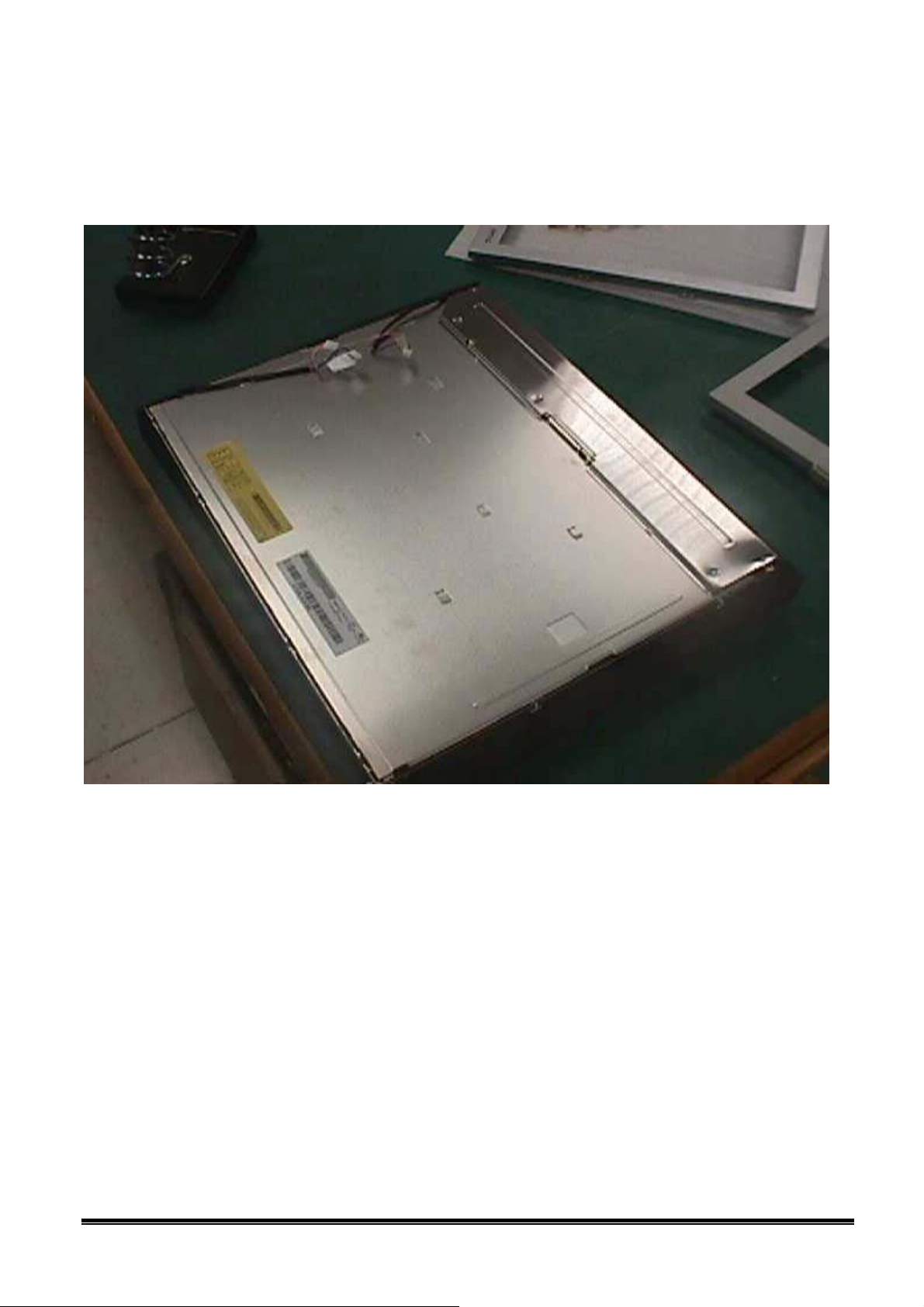
4. Wire Dressing and assembling concern
Prepare 1 panel
Alignment Procedure
Assembly panel and main BKT
7
Confidential
Page 8
Q7T4-FP71G LCD Monitor Service Guide
Alignment Procedure
Add 4 screw between panel and main BKT
8
Confidential
Page 9
Q7T4-FP71G LCD Monitor Service Guide
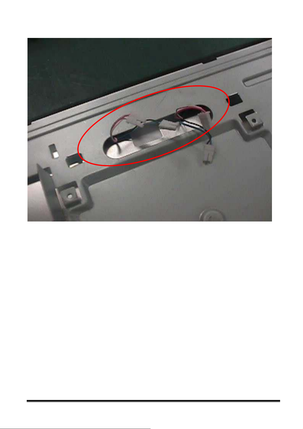
Alignment Procedure
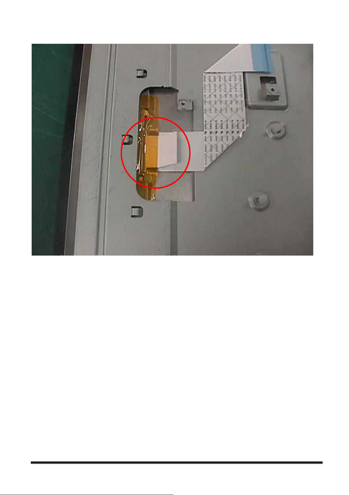
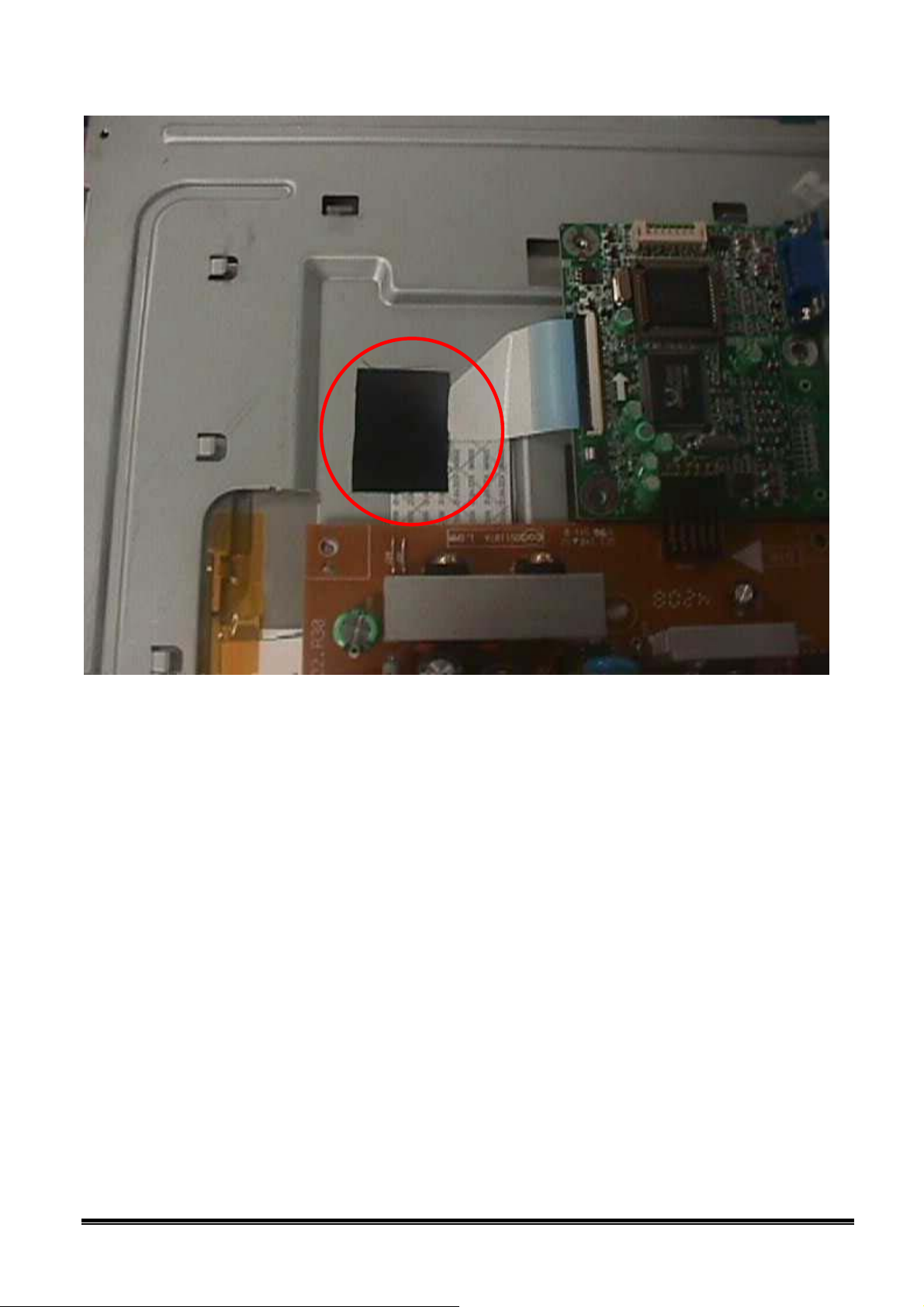
Add FFC
9
Confidential
Page 10
Q7T4-FP71G LCD Monitor Service Guide
Alignment Procedure
Add Tape
10
Confidential
Page 11
Q7T4-FP71G LCD Monitor Service Guide
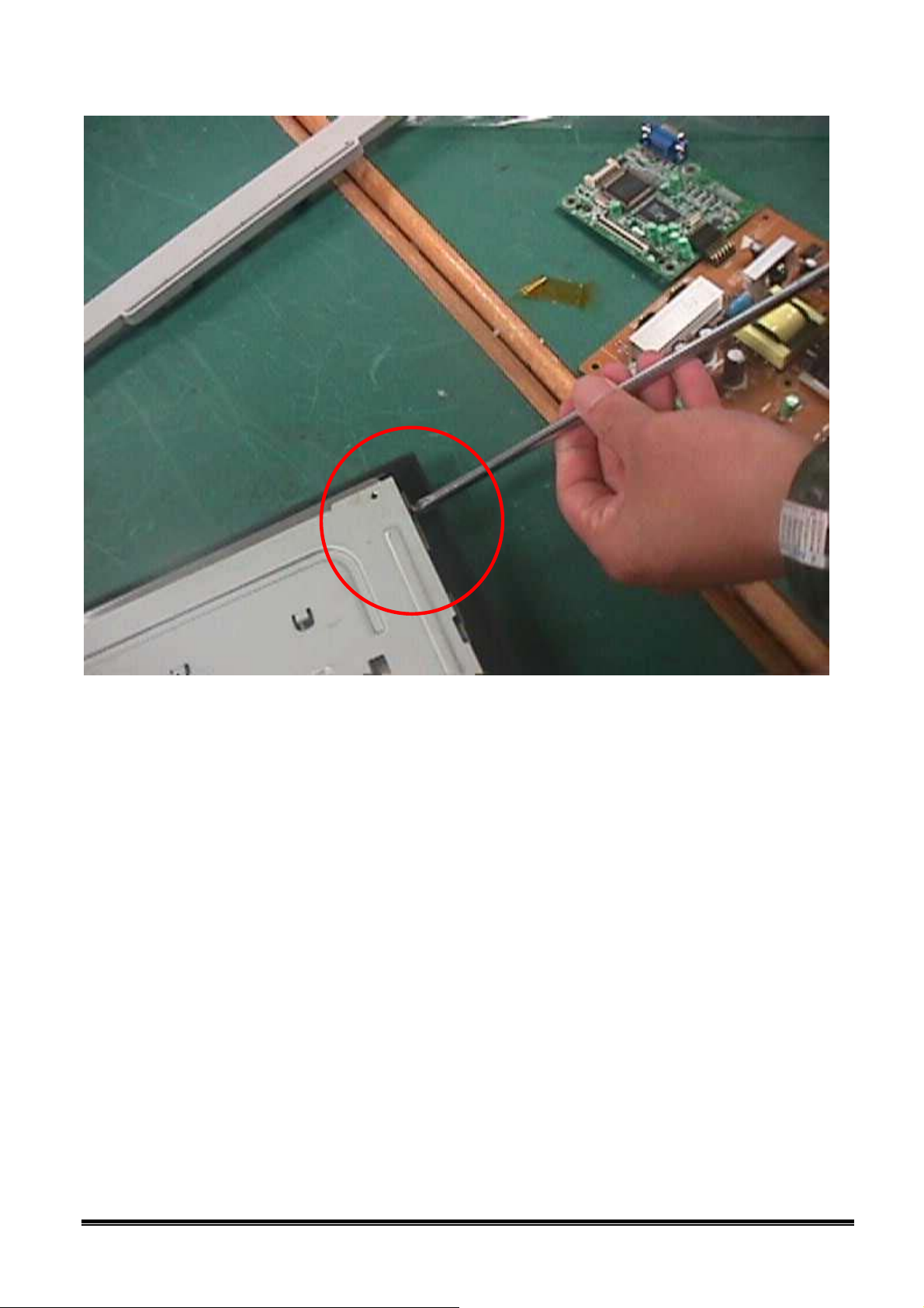
Alignment Procedure
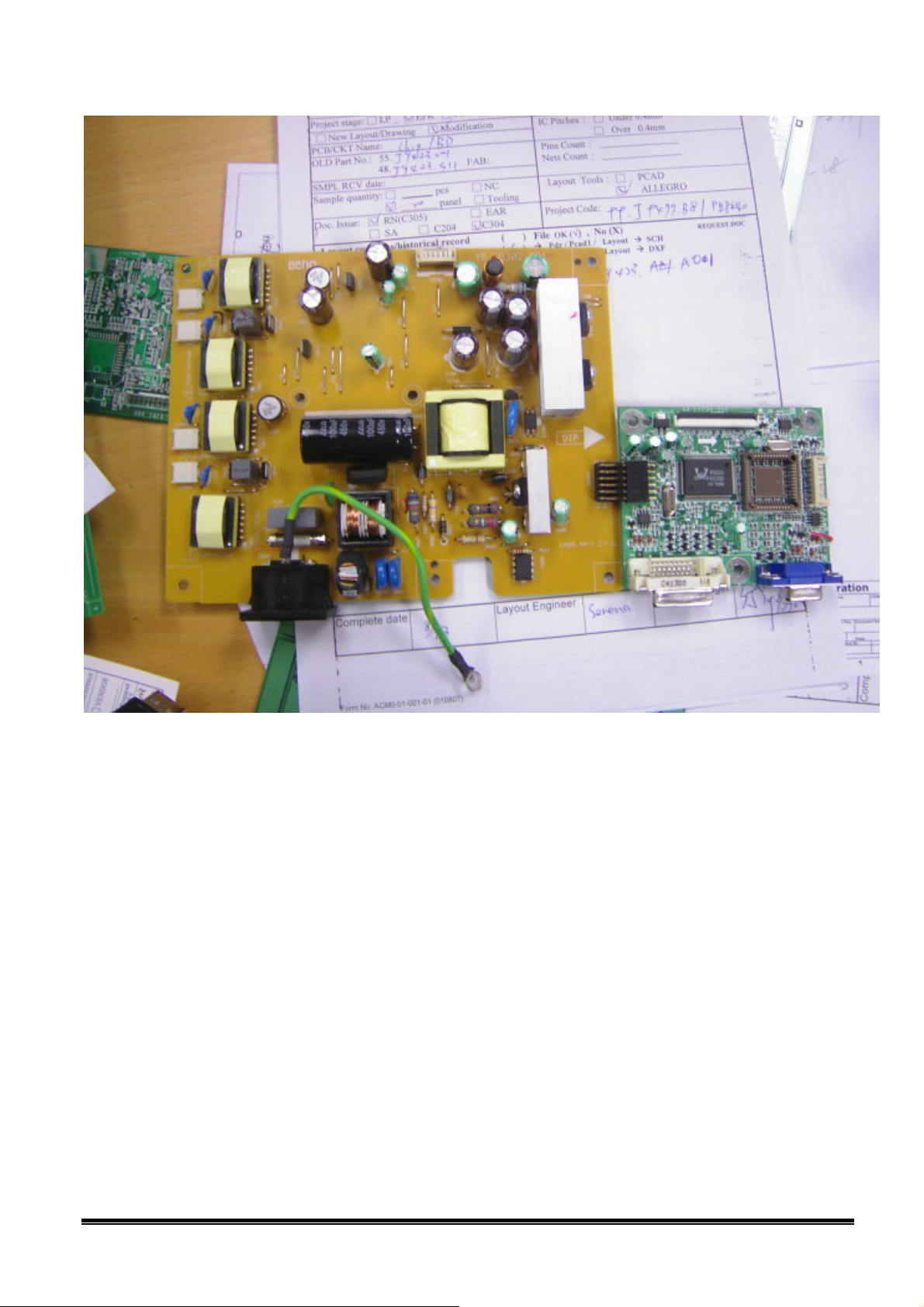
Assembly IF board and Power Board
11
Confidential
Page 12
Q7T4-FP71G LCD Monitor Service Guide
Alignment Procedure
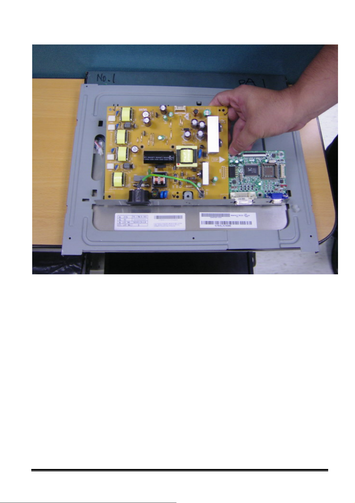
Assembly PCB module and main BKT
12
Confidential
Page 13
Q7T4-FP71G LCD Monitor Service Guide
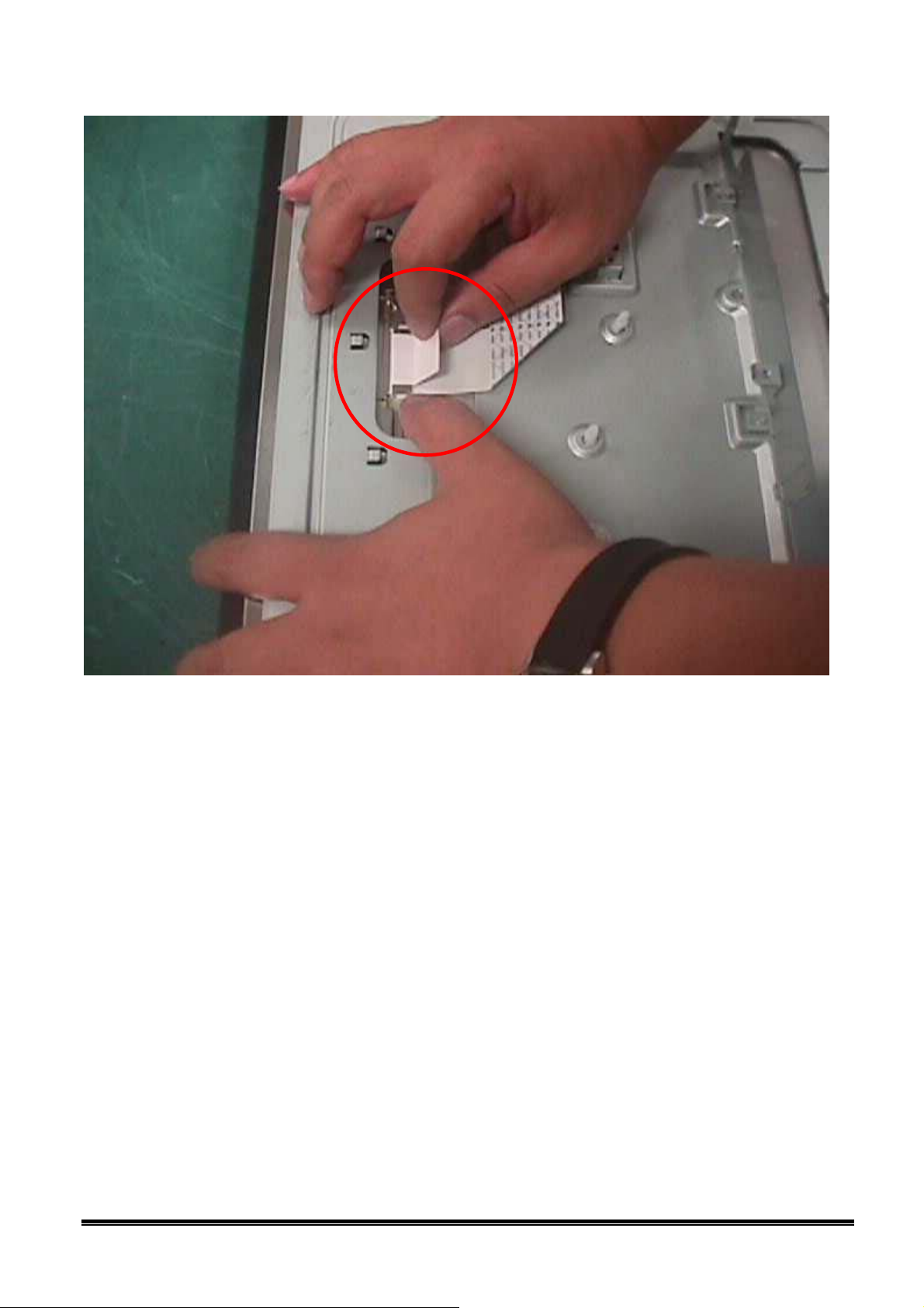
Alignment Procedure
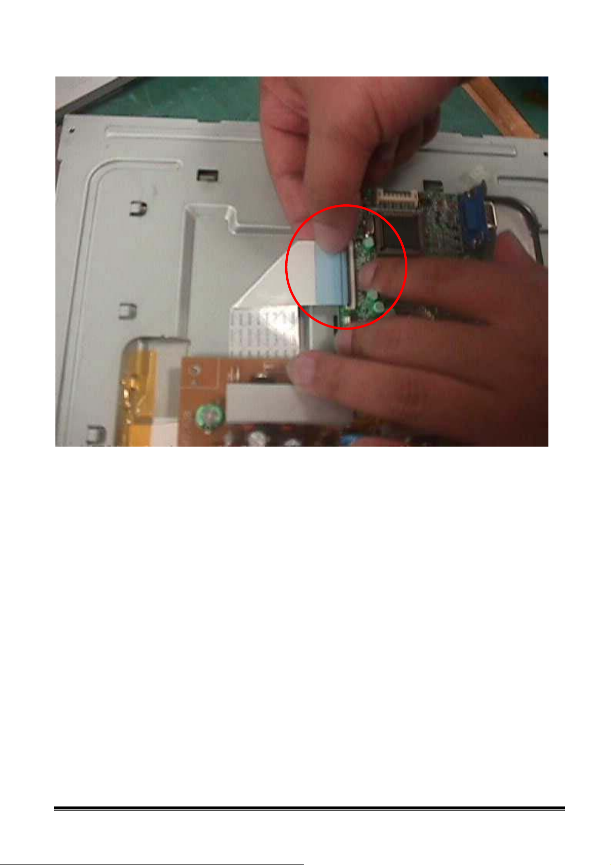
Assembly IF board and FFC
13
Confidential
Page 14
Q7T4-FP71G LCD Monitor Service Guide
Alignment Procedure
Add one tape
14
Confidential
Page 15
Q7T4-FP71G LCD Monitor Service Guide
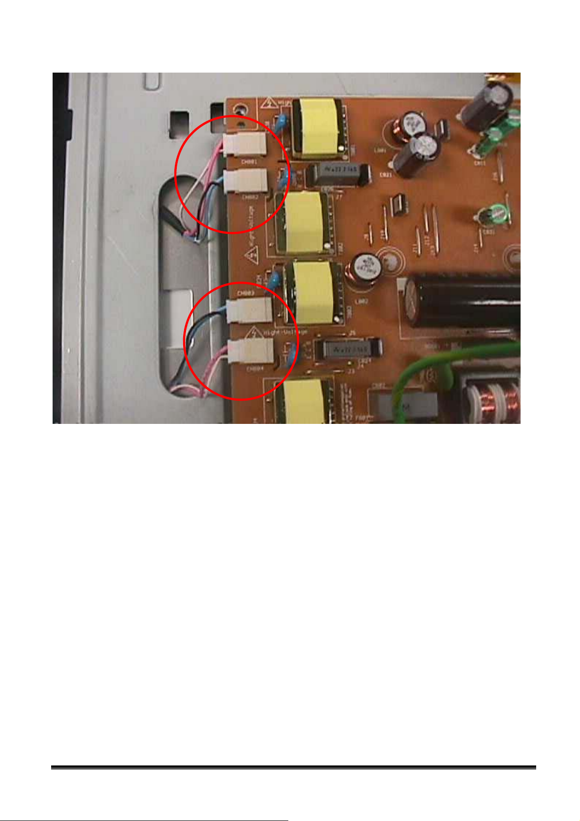
Alignment Procedure
Assembly lamp wire and Power Board
15
Confidential
Page 16
Q7T4-FP71G LCD Monitor Service Guide
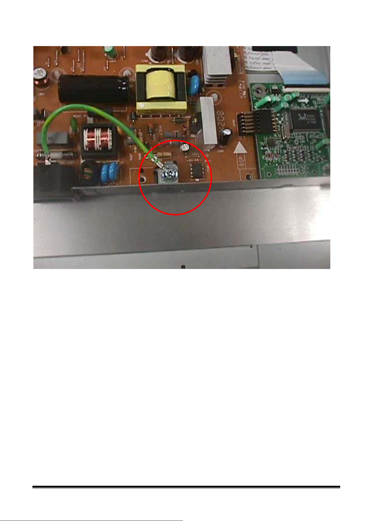
Alignment Procedure
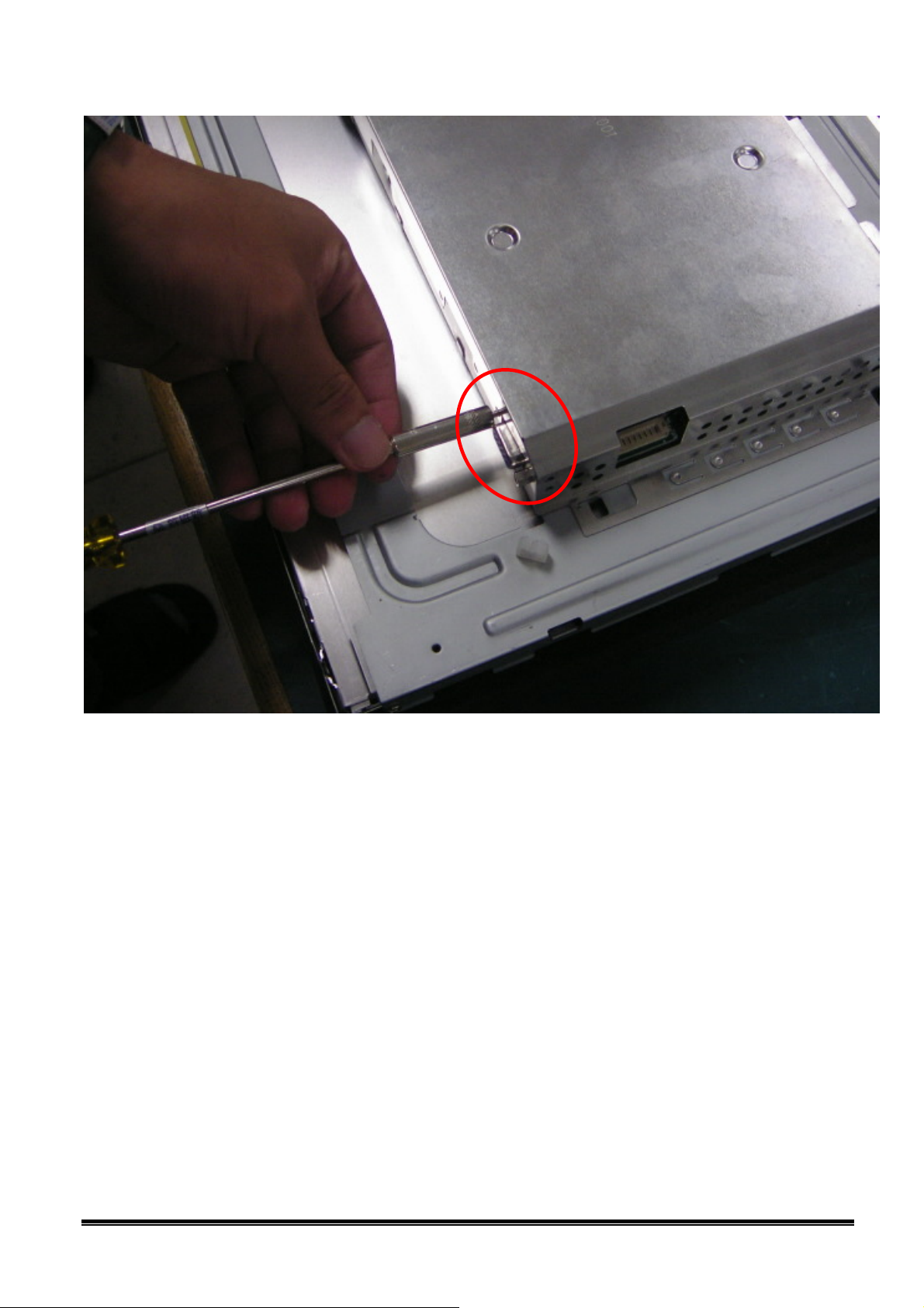
Add one screw
16
Confidential
Page 17
Q7T4-FP71G LCD Monitor Service Guide
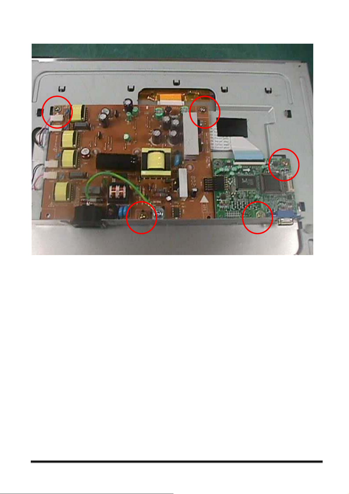
Alignment Procedure
Add 5 screw
17
Confidential
Page 18
Q7T4-FP71G LCD Monitor Service Guide
Alignment Procedure
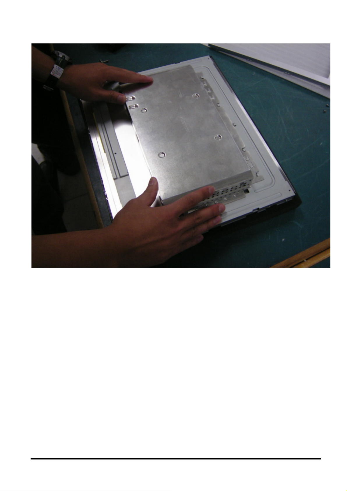
Assembly main shielding and main BKT
18
Confidential
Page 19
Q7T4-FP71G LCD Monitor Service Guide
Alignment Procedure
Add 2 screw
19
Confidential
Page 20
Q7T4-FP71G LCD Monitor Service Guide
Alignment Procedure
Assembly control board wire and IF board
20
Confidential
Page 21

Q7T4-FP71G LCD Monitor Service Guide
Alignment Procedure
21
Confidential
Page 22

Q7T4-FP71G LCD Monitor Service Guide
Alignment Procedure
Add one tape
22
Confidential
Page 23

Q7T4-FP71G LCD Monitor Service Guide
Alignment Procedure
Assembly Bezel and Rear Cover
23
Confidential
Page 24

Q7T4-FP71G LCD Monitor Service Guide
Alignment Procedure
Add 4 screw
24
Confidential
Page 25

Q7T4-FP71G LCD Monitor Service Guide
Alignment Procedure
Add 1 screw
25
Confidential
Page 26

Q7T4-FP71G LCD Monitor Service Guide
Alignment Procedure
Assembly Base and Rear cover
26
Confidential
Page 27

Q7T4-FP71G LCD Monitor Service Guide
Alignment Procedure
Finished
27
Confidential
Page 28

Q7T4-FP71G LCD Monitor Service Guide
Alignment Procedure
28
Confidential
Page 29

Q7T4-FP71G LCD Monitor Service Guide
Alignment Procedure
29
Confidential
Page 30

Q7T4-FP71G LCD Monitor Service Guide
Circuit Operation Theory
I. Introduction:
The Q7T4 is a 17” SXGA (1280x1024) , 16.2M colors(R, G, B 6-bit data+FRC data) TFT
LCD monitor. It’s an analog only interface LCD monitor with a 15 pins D-sub signal cable. it’s
compliant with VESA specification to offer a smart power management and power saving function. It
also offers OSD menu for users to control the adjustable items and get some information about this
monitor, and the best function is to offer users an easy method to set all adjustable items well just by
pressing one key, we called it “Auto key” which can auto adjusting all controlled items. Q7T4 also
offer DDC2 function to meet VESA standard.
II. Block diagram
The Q7T4 consists of a LCD module with 4 lamps, an power board, a control board ,and a
interface BD. The block diagram is shown as below.
LCD module with 4 lamps (backlight)
Inverter
Power
Interface board
Control board
D-Sub
AC power in
III. Circuit operation theory:
A-1.) Interface board diagram:
1
Confidential
Page 31

Q7T4-FP71G LCD Monitor Service Guide
MTV312M
64(AJ)
Circuit Operation Theory
Clock
Generator
D-SUB
140MHz
ADC
(a) Circuit operation theory:
A basic operation theory for the interface board is to convert input signal into digital RGB .
RTD 2023
XGA
1280×1024
LCM
Keypad IIC
Analog RGB signal is converted to digital signal through ADC. The microprocessor RTD2023
receives video data and optimizes the image automatically. It also supports 16 color from a 64k
palette bitmap OSD, and keypad controlling. The output data are sent to LCD module.
(b) IC introduction:
1.) DDC (Display Data Channel) function: We use DDC IC to support DDC/2B function. DDC
data is stored in 24C04(EEPROM). Those data related to LCD monitor specification. PC
can read them by “SDA” and “SCL” serial communication for I²C communication for
DDC2B.
2.) RTD2023 IC: There are triple ADC, LVDS transmitter ,Scaling, and OSD functions in the
RTD2023 IC. Scaling IC is revolutionary scaling engine, capable of expanding any source
resolution to a highly uniform and sharp image, combined with the critically proven
integrated 8 bit triple-ADC and patented Rapid-lock digital clock recovery system. It also
2
Confidential
Page 32

Q7T4-FP71G LCD Monitor Service Guide
support detect mode and DPMS control.
3.) MTV312M64: To stored the source code which is accessed by MCU to run program.
4.) EEPROM: We use 24C04 to store all the adjustable data and user settings.And use 24C02 to
store DVI EDID data.
A-2.) Control board introduction:
There are 6 keys for user's control which includes “Power”, “Enter”, “Up/Plus”,
“Down/Minus” , “Exit”, and “iKey” . The following descriptions are the introduction of these keys.
(1) Power key: to turn/off power of monitor
(2) “Enter” key: to enter sub-menus or select items.
(3) “Up/Plus key: to select previous and to increase adjustment
(4) “Down/Minus” key: to select next and to decrease adjustment
(5) “Exit” key: to back to previous menu, or leave OSD (auto save)
(6) “iKey”: to perform auto adjustment
(7) LED:
It indicates the DPMS status of this LCD monitor; green light means DPMS on (Normal
operating condition). Amber light means DPMS off (Powersaving).
Circuit Operation Theory
A-3.) Power board diagram:
EMI Filter Rectifier and
PWM controller
filter
Isolation power
transformer
Switching element
Rectifier and filter
Rectifier and filter
Inverter circuit
LDO regulator
Feedback Isolation
Fig.1
3
Confidential
Page 33

Q7T4-FP71G LCD Monitor Service Guide
Circuit Operation Theory
#1 EMI Filter
This circuit (fig. 2) is designed to inhibit electrical and magnetic interference for meeting FCC, VDE,
VCCI standard requirements.
Fig. 2
#2 Rectifier and filter
AC Voltage (90-264V) is rectified and filtered by BD601, C605 (See Fig 3) and the DC Output
voltage is 1.4*(AC input). (See Fig.3)
Fig. 3
4
Confidential
Page 34

Q7T4-FP71G LCD Monitor Service Guide
#3 Switching element and Isolation power transformer
When the Q601 turns on, energy is stored in the transformer.
During Q601 turn-off period, the stored energy is delivered to the
secondary of transformer. R607, C607 and D601 is a snubber circuit.
R615 is current sense resistor to control output power. (See Fig.4)
Circuit Operation Theory
Fig. 4
#4 Rectifier and filter
D701 and C703 are to produce DC output. L701 is used to suppress high Frequency switching spikes.
(See Fig.5)
Fig. 5
5
Confidential
Page 35

Q7T4-FP71G LCD Monitor Service Guide
#5 PWM Controller
The PWM controller NCP1200A implements a standard current mode architecture. With an
internal structure operating at a fixed 40KHz. Where the switch time is
dictated by the peak current set-point. When the current set-point falls
below a given value. The output power demand diminishes, the IC
automatically enters the so-called skip cycle mode and provides
excellent efficiency.
Circuit Operation Theory
Fig. 6
#6 Feedback circuit
PC123 is a photo-coupler and TL431 is a shunt regulation. They are
used to detect the output voltage change and be the primary and
secondary isolation. When output voltage changes, the feedback voltage
will be compared and duty cycle will be decided to control the correct
output voltage. (See Fig.7)
6
Confidential
Page 36

Q7T4-FP71G LCD Monitor Service Guide
A-3.) Control board introduction:
The main parts of the control board are a push button, and a LED.
(a) Push button:
It’s a simple switch function, pressing it for “ON” to do the auto
adjustment function, releasing it for “OFF” to do nothing.
(c) LED:
It indicates the DPMS status of this LCD monitor; green light means DPMS on
(Normal operating condition). Amber light means DPMS off (Power off condition).
Circuit Operation Theory
Fig. 7
7
Confidential
Page 37

Q7T4-FP71G LCD Monitor Service Guide
A-4.) Inverter diagram:
1.Block Diagram:
Circuit Operation Theory
15Vin
ON/OFF
BRT_ADJ
ON/OFF
switching
PWM CONTROLLER
TL1451 CIRCUIT
2. General Specification
Input Voltage: 15V
Input Current: 2A max.
ON/OFF Voltage: 5V
PWM Duty: 5V/50KHz
Output Requirement:
Max. Output Current: 7.5mA
Min. Output Current: 3.3mA
OSCILATOR
CIRCUIT
TRANSFORMER CCFL
PROTECTION
AND DETECT
Lamp Working Voltage: 660Vrms
Open Lamp Voltage: 1500Vrms
Frequency: 50KHz
8
Confidential
Page 38

Q7T4-FP71G LCD Monitor Service Guide
Circuit Operation Theory
3.Circuit Operation Theorem
3.1 ON/OFF SWITCH
The turn-on voltage was controlled by R815 and R816.The inverter was turned on or off by the
switching transistors Q801 and Q802.
9
Confidential
Page 39

Q7T4-FP71G LCD Monitor Service Guide
3.2 PWM Control circuit
Circuit Operation Theory
TL1451 is a dual PWM controller.C807 and R811 decide the working frequency.BLT_ADJ signal is
from control board, control pulse width then decide how much energy delivery to CCFL also decide
CCFL brightness. Q810 and Q811 be the buffer to rise the drive capability and the totem poles
circuit can improve a capable of driving for Q812.C813 decide the striking time delay.
10
Confidential
Page 40

Q7T4-FP71G LCD Monitor Service Guide
Circuit Operation Theory
3.3 Oscillator Circuit
Royer circuit uses the characteristic of transformer saturation to oscillate. When the DC power inject,
Q808 or Q809 will turns on, and the current Ic increases. After a period, the transistor will leave the
saturation status and Vce increase. The result causes the voltage of primary coil get lower. Finally the
transistor turn off, and another transistor turn on. These statuses are repeated and the pin7 and pin8 of
T801 will get a sine wave to turn on CCFL.
11
Confidential
Page 41

5
4
3
2
1
D D
C C
B B
CON 301
1
2
3
4
5
6
7
8
9
10
20600 89110
KEY_EXIT
KEY_ LEFT
BL U
OR G
KEY_ RI GHT
KEY_ MENU
PW_S W
LED3 01 BL U/ORG
BL U
A2
A1
KEY_ MENUI _K EY
J
KEY_ RI GHTOR G
KEY_ LEFT
PW_S W
KEY_EXIT
I _K EY
SW3 01 22 40069431
1 2
G2G1
SW3 02 22 40069431
1 2
G2G1
SW3 03 22 40069431
1 2
G2G1
SW3 06 22 40069431
1 2
G2G1
SW3 04 22 40069431
1 2
G2G1
SW3 05 22 40069431
1 2
G2G1
LED use 06.3N5YG.14X;
Key use 22.40069.431
Pro jec t Co de
99. L1C72.001
A A
5
4
3
Title
Size Doc ument Nu mb er R e v .
PCB P/ N
<Size>
Da te : Sheet
2
48. L1C03.S02
Thu rsd ay , A ugu st 26, 2004
Pre par ed By
ANGE L HU
Mod el Na me
Q7T4
CTRL BOA RD
PC B R ev.
S02
Re vi ew e d B y Ap pr ov ed By
ALL EN PC LEE DA VE N WU
OEM /ODM Mode l Nam e
99.L 1C72. 000- C3-30 4-00 2
1 1
1
NA
0
o f
Page 42

Q7T4-FP71G LCD Monitor Service Guide
Engineering Specification
Table of Contents
1. Introduction 3
2. Operational Specification 3
2.1 Power supply.................................................................................................................................3
2.2 Signal interface .............................................................................................................................4
2.3 Video performance........................................................................................................................5
2.4 Scan range.....................................................................................................................................6
2.5 Plug & Play DDC2B Support .......................................................................................................6
2.6 Support Timings............................................................................................................................6
3. Operational & Functional Specification 7
3.1 Video performance........................................................................................................................7
3.2 Brightness Adjustable Range........................................................................................................7
3.3 Acoustical Noise ...........................................................................................................................7
3.4 Environment..................................................................................................................................7
3.5 Transportation...............................................................................................................................7
3.6 Electrostatic Discharge Requirements...........................................................................................8
3.7 EMC..............................................................................................................................................8
3.8 Reliability......................................................................................................................................8
3.9 Audio performance........................................................................................................................9
4. LCD Characteristics 9
4.1 The Physical definition & Technology summary of LCD panel...................................................9
4.2 Optical characteristics of LCD panel............................................................................................9
5. User Controls 10
5.1 User’s hardware control definition................................................................................................10
5.2 OSD control function definition....................................................................................................10
6. Mechanical Characteristics 11
6.1 Dimension.....................................................................................................................................11
6.2 W eight...........................................................................................................................................11
6.3 Plastic............................................................................................................................................11
6.4 Carton............................................................................................................................................12
1
Confidential
Page 43

Q7T4-FP71G LCD Monitor Service Guide
Engineering Specification
Table of Contents
7. Pallet & Shipment 12
7.1 Container Specification.................................................................................................................12
7.2 Carton Specification......................................................................................................................12
Product:.................................................................................................................................12
Package:................................................................................................................................ 12
8. Certification 12
Appendix: Physical Dimension Front View and Side view 14
2
Confidential
Page 44

Q7T4-FP71G LCD Monitor Service Guide
N
Engineering Specification
1. Introduction
This specification describes Q7T4, which is a 17.0” analog interface color TFT LCD monitor without audio. The
monitor supports up to 1280x1024 pixel resolution and refresh rate of 75 Hz. The independent 6 bits R, G, B
colors are capable of displaying 16.2M colors (RGB-6bit + FRC data). In addition, dithering function is
supported. The features summary is shown below,
*All panel spec. in C201 definition depends on the variance of panel source.
Feature items Specifications Remark
Panel supplier & module name
Screen diagonal 17.0” (432mm) 337.920(H) x 270.336(V)
Display Format SXGA / 1280 (H) x 1024 (V)
Pixel Pitch 0.264 mm x 0.264 mm
Viewing Angle (@ Contrast Ratio = 10)
Analog interface with Scaling supported
DVI interface with Scaling supported
Video interface with Scaling supported No
Max resolution mode supported 1280 x 1024 @ 75Hz
umber of Display Colors supported 16.2M colors (RGB 6-bits + FRC data)
Contrast Ratio
Luminance
AC power input
DC power input (with AC power adapter) No
DPMS supported
LED indicator for power status showed
OSD for control & information supported
Multi-language supported for OSD
Buttons control supported
Flywheel control supported No
Scaling function supported
Auto adjustment function supported
DDC function supported (EDID ver. 1.3)
Audio speakers supported
Audio Jack (input connector) supported
Earphone Jack (input connector) supported
Microphone function supported No
Mechanical Tilt base design
VESA wall mounting design
Mechanical Rotate design No
Mechanical Lift base design No
Kensington compatible lock design
AUO M170EG01
R/L: 70/70 degrees (typ.)
and U/D: 70/60 degrees (typ.)
Yes
No
450:1 (typ.)
2
260 cd/m
(typ.)
Yes
Yes
Yes
Yes
Yes
Yes
Yes
Yes
Yes
No
No
No
Yes
Yes
Yes
Further divided into v.0 and v.1
versions (spec v.1)
Panel spec.
With 15-pin D-sub connector
White Luminance@CCFL
7.5mA (center)
90-264 Volts, 47-63 Hz.
≤ 1W at 115±5 VAC
≤2W at 230 VAC in Power off
Preferred Mode
Green/Amber/Non
8 languages
6 buttons including 1 monitor
power on/off control button.
“i-key” function
DDC2B only
From -5 to +20 degree
2. Operational Specification
2.1 Power supply
3
Confidential
Page 45

Q7T4-FP71G LCD Monitor Service Guide
Item Condition Spec OK N.A Remark
Input Voltage range
Input Current range
Power Consumption
DPMS
Inrush Current
Earth Leakage Current
Hi-Pot
Power Line Transient
CCFL operation range
CCFL Frequency
Power cord
Universal input full range 90~264VAC /47~63Hz
90 ~ 264VAC < 2.0 Arms
Normal “On” operation < 40 W
DPMS “Off” state
110 VAC
220 VAC
264 VAC/50Hz < 3.5 mA
1. 1500VAC, 1 sec
2. Ground test: 30A, 1sec
IEC1000-4-4 1KV √
IEC1000-4-5 (Surge)
90 ~ 264VAC 3 mA ~8mA
90 ~ 264VAC 40KHz ~ 80KHz
Engineering Specification
<
1 W in power preferred
mode, 115V
2 W, 230V
<
< 30 A (peak)
< 60 A (peak)
Without damage
< 0.1 ohm
Common: 2KV,
Differential: 1KV
Color: Black
Length: 1500
+/- 50 mm
√
√
LED: Green
√
LED: Amber
√
Cold-start
√
√
(on-line test)
√
√
√
√
√
(in-lab test)
Panel Spec.
3.0 ~ 8.0mA rms
Panel Spec.
40KHz ~ 80KHz
2.2 Signal interface
Item Condition Spec OK N.A Remark
Signal Cable
Pin assignment
Sync input
15-pin D-Sub
24-pin DVI-D
15-pin D-sub connector
24-pin DVI-D connector
Signal type
Level
Impedance
Signal type
Level
Impedance
Sync Pulse Width (SPW)
Color: Black
Length: 1500
Color: Black
Length: 2000
Separate analog R/G/B
700 mV (peak to peak)
75 Ohms +/- 1.5 Ohms
Separate H/V-sync
Composite H/V-sync
(Positive/Negative)
Logic High: 2.4V ~ 5.5V
Logic Low: 0V ~ 0.5V
(TTL level)
Minimum 2.2K
0.7μs < H-SPW
1H < V-SPW
+/-
+/-
See Note-1
See Note-2
Ω(pull down)
30 mm
50 mm
√
√
√
√
√
√
For 15-pin D-sub
For 24-pin DVI-D
√
For 15-pin D-sub
Video input
√
√
√
√
For 15-pin D-sub
Refer to VESA VSIS
Standard V1R1
10KΩ for application
Note-1: The pin assignment of 15-pin D-sub connector is as below,
1 5
6
11 15
10
4
Confidential
Page 46

Q7T4-FP71G LCD Monitor Service Guide
Pin Signal Assignment Pin Signal Assignment
1 Red video 9 PC5V (+5 volt power)
2 Green video 10 Sync Ground
3 Blue video 11 Ground
4 Ground 12 SDA
5 Cable Detected 13 H-Sync (or H+V)
6 Red Ground 14 V-sync
7 Green Ground 15 SCL
8 Blue Ground
Engineering Specification
Note-2: The pin assignment of 24-pin DVI-D connector is as below,
Pin Signal Assignment Pin Signal Assignment
1 TMDS RX2- 13 Floating
2 TMDS RX2+ 14 +5V Power
3 TMDS Ground 15 Ground
4 Floating 16 Hot Plug Detect
5 Floating 17 TMDS RX06 DDC Clock 18 TMDS RX0+
7 DDC Data 19 TMDS Ground
8 Floating 20 Floating
9 TMDS RX1- 21 Floating
10 TMDS RX1+ 22 TMDS Ground
11 TMDS Ground 23 TMDS Clock+
12 Floating 24 TMDS Clock-
2.3 Video performance
Item Condition Spec OK N.A Remark
Max. support Pixel rate
Max. Resolution
< 6.25 ns
Rise time + Fall time
Settling Time after
overshoot /undershoot
Overshoot/Undershoot
< 12% of step function
< 5% final full-scale value
voltage level over the full
5
Confidential
135 MHz
1280 x 1024
(50% of minimum pixel
clock period)
voltage range
√
√
√
√
√
1280 x 1024 @ 75Hz
(max. support timing)
Refer to VESA VSIS
Standard V1R1
Refer to VESA VSIS
Standard V1R1
Page 47

Q7T4-FP71G LCD Monitor Service Guide
OS
OS
OS
VES
VES
VES
VES
VES
VES
VES
VES
VES
SU
SU
VES
VES
S
2.4 Scan range
Item Condition Spec OK N.A Remark
Horizontal
Vertical
2.5 Plug & Play DDC2B Support
Item Condition Spec OK N.A Remark
DDC channel type
EDID
2.6 Support Timings
30 ~ 83 KHz
56 ~ 76 Hz
DDC2B
Version 1.3
Engineering Specification
√
Without Frame buffer
√
√
Refer to Q7C4 S/W
√
spec. document to see
the detailed EDID data
definition.
Input Timing
Resolution
640x350 31.47(P) 70.08(N) 25.17 1280x943
720x400 31.47(N) 70.08(P) 28.32 1280x1024
640x480 31.47(N) 60.00(N) 25.18 1280x1024
640x480 35.00(N) 67.00(N) 30.24 1280x1024
640x480 37.86(N) 72.80(N) 31.5 1280x1024
640x480 37.50(N) 75.00(N) 31.5 1280x1024
800x600 37.88(P) 60.32(P) 40.00 1280x1024
800x600 48.08(P) 72.19(P) 50.00 1280x1024
800x600 46.86(P) 75.00(P) 49.50 1280x1024
832X624 49.72(N) 74.55(N) 57.29 1280x1024
1024x768 48.36(N) 60.00(N) 65.00 1280x1024
1024x768 56.48(N) 70.10(N) 75.00 1280x1024
1024x768 60.02(P) 75.00(P) 78.75 1280x1024
1024X768 60.24(N) 74.93(N) 80.00 1280x1024
1152x864 67.50(P) 75.00(P) 108.00 1280x1024
1152x870 68.68(N) 75.06(N) 100.00 1280x1024
1152x900 61.80(N) 66.00(N) 94.50 1280x1024
1152x900 71.81(N) 76.14(N) 108.00 1280x1024
1280x1024 64.00(P) 60.00(P) 108.00 1280x1024
1280x1024 75.83(N) 71.53(N) 128.00 1280x1024
1280x1024 80.00(P) 75.00(P) 135.00 1280x1024
1280x1024 81.18(N) 76.16(N) 135.09 1280x1024
Horizontal Vertical Dot Clock Actual display
Actual Output
OK N.A
√
√
√
√
√
√
√
√
√
√
√
√
√
√
√
√
√
√
√
√
√
√
Remark
D
D
D
Macintosh
A
A
A
A
A
Macintosh
A
A
A
Macintosh
A
Macintosh
N 66
N
A
IBM1
A
PARC2
Note-3: “P”, “N” stands for “Positive”, “Negative” polarity of incoming H-sync/V-sync (input timing).
6
Confidential
Page 48

Q7T4-FP71G LCD Monitor Service Guide
p
3. Operational & Functional Specification
3.1 Video performance
Item Condition Spec OK N.A Remark
Resolution
Contrast ratio
Brightness
Response time
Viewing angle
CIE coordinate of White
Display colors
Any input resolution modes
which are under 1280 x 1024
450:1 (typ.)
At R/G/B saturated condition 260 cd/m2 (typ.) @ 7.5mA
Rising + Falling time 16 ms (typ.)
At Contrast ratio = 10 R/L: 70/70 degrees (typ.)
At Contrast ratio = 10 U/D: 70/60 degrees (typ.)
(0.31, 0.33) +/- (0.03, 0.03)
3.2 Brightness Adjustable Range
Item Condition Spec OK N.A Remark
At default contrast level
Brightness adjustable range
(saturate point) & Full-white
color pattern
Engineering Specification
1280 x 1024
16.2M colors
(RGB 6-bits + FRC data)
(Max. brightness value –
Min. brightness value)
≧ 100 cd/㎡
√
√
√
√
√
√
√
Support dithering
√
√
3.3 Acoustical Noise
Item Condition Spec OK N.A Remark
Acoustical Noise
3.4 Environment
Item Condition Spec OK N.A Remark
Temperature
Humidity
Altitude
3.5 Transportation
Item Condition Spec OK N.A Remark
(1) Vibration
At 1 meter distance
& “Audio” function disabled
Operating
Non-operating
Operating 10 ~ 90%
Non-operating 5 ~ 95%
Operating 0~3048m (10,000ft)
Non-operating 0~12,192m (40,000ft)
(1) Sine wave
5~200Hz 1.5G, 1 octave/min,
15 min dwell on each resonant
Package, Non-Operating
frequency, all primary axis,
one sweep (30 min minimum)
er orientation, total of 90+
min.
≦ 40 dB/A
0 ~ +40 ℃
-20 ~ +60 ℃
√
√
√
Non-condensing
√
Non-condensing
√
Without packing
√
With packing
√
√
7
Confidential
Page 49

Q7T4-FP71G LCD Monitor Service Guide
(2) Unpackaged Vibration
(3) Drop
(4) Shock
Unpackaged, Non-Operating
Package, Non-Operating
Wooden package,
Non-Operating
Engineering Specification
(2) Random
5 ~100 Hz, 0 dB/Oct. 0.015
2
/Hz
g
100 ~200 Hz, -6 dB/Oct.
200 Hz, 0.0038 g
Equivalent to 1.47 Grms, All
primary axis, 20 min perorientation, total is 60 min.
(3) Procedure:
Confirmed sample with
appearance and function ready
before testing then compare
with after test record as
brightness, uniformity and
contrast ratio. Perform
random vibration after
sine-wave vibration test.
Test Spectrum:
20 Hz 0.0185(g2/Hz)
200Hz 0.0185(g2/Hz)
Duration : 5 Minutes
Axis : 3 axis ( Horizontal
and Vertical axis ,Z axis)
91 cm Height (MP stage)
(1 corner, 3 edges, 6 faces)
Waveform: half sine
Faces: 6 sides/ per orientation
3 shocks.
Duration: <3ms
Velocity accelerate: 75g
2
/Hz
√
√
√
3.6 Electrostatic Discharge Requirements
Item Condition Spec OK N.A Remark
Electrostatic Discharge
3.7 EMC
Item Condition Spec OK N.A Remark
TCO03
EMI
3.8 Reliability
Item Condition Spec OK N.A Remark
MTBF Prediction
CCFL Life time
IEC801-2 standard
Electric
Magnetic
FCC part 15J class B
EN55022 class B
Refer to MIL-217F > 60,000 Hours
At 25±2℃, under 7.0mA
After Mass production under
1dBuv for constant measure.
Besides DNSF and VCCI
class-2 are optional.
Contact: 8KV
Air: 15KV
Band 1 < 10 V/m
Band 2 < 1 V/m
Band 1 < 200nT
Band 2 < 25nT
50,000 Hours (typ.)
√
√
√
√
Excluding CCFL
√
See Note-4
√
Note-4: CCFL lifetime is determined as the time at which brightness of lamp is 50%. The typical lifetime of
CCFL is on the condition at 7.5mA lamp current.
8
Confidential
Page 50

Q7T4-FP71G LCD Monitor Service Guide
3.9 Audio performance
Item Condition Spec OK N.A Remark
Preamp + Power amp
(1)Output power
(2)THD (@ 1W)
(3)S/N ratio
Speaker Driver
(1)Nominal impedance
(2)Rated input power
(3)Frequency response
(4)Output sound pressure level
(5)Dimension of box
Audio Control
(1)Volume range
(2)Mute
Engineering Specification
1 Wrms/CH @ 1KHz
<1%
>40dB
8 ohm
2 W/CH
180~20KHz SPL-10dB
84 ± 3 dB (1W 0.5M)
62x33cx20 mm
0 ~100 levels
On/Off
2
√
√
√
√
√
√
√
√
√
√
4. LCD Characteristics
4.1 The Physical definition & Technology summary of LCD panel
Item Condition Spec OK N.A Remark
LCD Panel Supplier
Panel type of Supplier
Screen Diagonal
Display area
Physical Size
Weight
Unit=mm 337.920(H) x 270.336(V)
Unit=mm 358.5(H) x 296.5(V) x 17.0 (D) (typ.)
Unit=gram 1900 (typ.)
Technology
Pixel pitch
Unit=mm 0.264 x 0.264
Pixel arrangement
Display mode
Support color
TN type
R/G/B vertical stripe
16.2M colors (RGB 6-bits + FRC data)
AUO
M170EG01 V1
432mm(17.0”)
Normally white
√
√
√
√
√
√
√
Per one triad
√
√
√
√
4.2 Optical characteristics of LCD panel
Item Unit Conditions Min. Typ. Max. Remark
Viewing Angle
Contrast ratio
Response Time
Color / Chromaticity
[degree]
[degree]
[degree]
[degree]
[msec] Rising Time - 12 20
[msec] Falling Time - 4 5
[msec] Rising + Falling - 16 25
Horizontal (Right)
CR = 10 (Left)
Vertical (Up)
CR = 10 (Down)
Normal Direction
Red x 0.61 0.64 0.67
Red y 0.31 0.34 0.37
60
60
60
50
250 450
70
70
70
60
-
-
-
-
9
Confidential
Page 51

Q7T4-FP71G LCD Monitor Service Guide
Engineering Specification
Green x 0.26 0.29 0.32
Coordinates (CIE)
Color Coordinates (CIE) White
Luminance Uniformity
White Luminance @ CCFL
7.5mA (center)
Crosstalk (in 75Hz)
* The test methods for the above items’ definition, please refer to the relative panel specification.
Green y 0.58 0.61 0.64
Blue x 0.11 0.14 0.17
Blue y 0.04 0.07 0.10
White x 0.28 0.31 0.34
White y 0.30 0.33 0.36
[%] 9 points measurement
[cd/m2]
[%]
75 80 -
210 260 -
1.5
5. User Controls
5.1 User’s hardware control definition
Item Condition Spec OK N.A Remark
Monitor Power button
Enter button
Right/Inc. button
Left/Dec. button
Exit /Volume button
I-key button
Mode Selection button
Mute button
Input source select button
√
√
√
√
√
√
√
√
√
5.2 OSD control function definition
Item Condition Spec OK N.A Remark
Auto Adjust
Brightness
Contrast
Horizontal Position
Vertical Position
Pixel Clock
Phase
Color
OSD Position
OSD Time
Language
Recall
Mode Selection
Auto-Geometry
Bluish
Reddish
sRGB
: Separate R/G/B adjustment
User
OSD Horizontal position
OSD Vertical position
From 5 sec to 60 sec
8 languages
Color recall
Recall All
√
√
√
√
√
√
√
√
√
√
√
√
√
10
Confidential
Page 52

Q7T4-FP71G LCD Monitor Service Guide
Engineering Specification
Input Select
Sharpness
Display Information
Volume
Mute
Hot key for Brightness
Hot key for Contrast
Hot key for Volume
Hot key for Mode
* The detailed firmware functions’ specification, please refer to C212 S/W spec. document.
D-sub
DVI
For input timing
√
√
√
√
6. Mechanical Characteristics
6.1 Dimension
Item Condition Spec OK N.A Remark
Bezel opening
Monitor without Stand
Monitor with Stand
Carton Box (outside)
Tilt and Swivel range
L x W x H mm
L x W x H mm
L x W x H mm
339.84 x 272.24 mm
323.75*378*60.5mm
362*378*135.31 mm
456(L)*423(W)*114(H)
Tilt: -5 ~ +20 degree
Swivel: 0 degrees
√
√
√
√
√
√
√
√
√
√
6.2 Weight
Item Condition Spec OK N.A Remark
Monitor (Net)
Monitor with packing
6.3 Plastic
Item Condition Spec OK N.A Remark
Flammability
Heat deflection To
UV stability
Resin
Texture
Color
(Gross)
ABS
ABS
(VW55/VE0856/D350)
3.8 Kg
5.7 Kg
94-HB
65 ℃
Delta E < 8.0
MPRII:
BCS-Y5003A
ABS
MT-11020
√
√
√
√
√
√
√
√
Bezel texture
MT-11000
Bezel painting
T8020C
11
Confidential
Page 53

Q7T4-FP71G LCD Monitor Service Guide
6.4 Carton
Item Condition Spec OK N.A Remark
Color
Material
Compression strength
Burst Strength
Stacked quantity
7. Pallet & Shipment
7.1 Container Specification
Quantity of products
Stowing Type Container
(sets)
(Every container)
Engineering Specification
Kraft
B Flute
288 KGF
(sets)
2
16 KGF/cm
18 Layers
Quantity of Products
(Every Pallet)
√
√
√
√
√
Quantity of pallet
(sets)
(Every Container)
With pallet
Without pallet
7.2 Carton Specification
Product:
Net Weight (Kg) Gross Weight (Kg)
Package:
20'
40'
20'
40'
3.8Kg 5.7Kg 323.75*378*60.5mm 362*378*135.31 mm
Carton Interior Dimension (mm)
L*W*H
1080 Pallet A: 90 Pallet A: 12
Pallet B: 72 Pallet B: 12
2520 Pallet A: 90 Pallet A: 14
Pallet B: 72 Pallet B: 14
X X
X X
X X
X X
Dimension w/o Base
L*W*H (mm)
Carton External Dimension (mm)
L*W*H
Dimension w/ Base
L*W*H (mm)
448(L)*415(W)*100(H) 456(L)*423(W)*114(H)
8. Certification
Item Condition Spec OK N.A Remark
Environment
12
Confidential
Green design
Blue Angel German Standard
E-2000 Switzerland
API Doc. 715-C49
√
√
√
ISO14000
Requirement
Page 54

Q7T4-FP71G LCD Monitor Service Guide
Engineering Specification
PC-Monitor
Safety
EPA USA Standard
TCO’99
TCO’03
Green Mark
Microsoft Windows PC98/99
DPMS VESA
DDC 2B Version 1.3
USB External
UL (USA) UL60950 3rd edition
CSA (Canada) CAN/CSA-C22.2 No. 60950
Nordic / D.N.S.F EN60950
FIMKO EN60950
CE Mark 73/23/EEC
IEC60950
EN60950
CB
EN60950
√
√
√
√
√
√
√
√
√
√
√
√
√
√
√
√
EMC
X- Ray Requirement
TUV/GS
EN60950 /
EK1-ITB 2000:2003
CCC (China)
GOST EN60950
SASO
CE Mark 89/336/EEC
FCC (USA) FCC Part 15 B
√
√
√
√
√
√
EN55022 Class B
√
CISPR 22 Class B
VCCI (Japan) VCCI Class B
BSMI (Taiwan) CNS 13438
C-Tick (Australia) AS/ NZS CISPR22
DHHS (21 CFR) USA X- Ray Standard
DNHW
PTB German X- Ray standard
√
√
√
√
√
√
√
√
√
√
Ergonomics
TUV / Ergo
ISO 13406-2
prEN50279
13
Confidential
Page 55

Q7T4-FP71G LCD Monitor Service Guide
Engineering Specification
Appendix: Physical Dimension Front View and Side view
Fig. 1 Physical Dimension Front View and Side view
14
Confidential
Page 56

5
3.3 V_MCU
D N1
BAV70 LT1
2
1
R1 3
4.7K
R1
4.7K
DD C_ WP_A
R2
4.7K
PC 5V
DS UB_S CL
DS UB_S DA
DS UB_S DA
DSU B_SC L
R1 4
47
R1 5
47
3
C2
0. 1U
U1
1
D D
2
3
4
A0
A1
A2
VSS
R1 0
AT24 C02A
8
VCC
7
WP
6
SCL
5
SDA
0
3.3 V_MCU
C C
J2
TP18
TP19
TP20
TP21
TP22
TP23
TP24
TP12
TP13
TP14
TP15
TP16
TP17
RX2RX1RX0RX2+
RX1+
RX0+
Hot -Plug
DVI _SC L
DVI PC5 V
DVI _SD A
R3 0
RXC+
10K
RXC-
D-d etec t
D6
6.2 V
1 2
D8
D7
6.2 V
6.2 V
ESD solution
1 2
1 2
C1 6
0.0 1U
3
1
1
9
9
17
17
2
2
10
10
18
18
3
3
11
11
19
19
4
4
12
12
20
20
5
5
13
13
21
21
6
6
14
14
22
22
7
7
B B
15
15
23
23
8
8
16
16
24
24
G1
G1
G2
G2
202 2009024
4
3
2
1
3.3 V_MCU
D N2
BAV 99
PC5 V
D1
6.2 V
1 2
11
TP5
12
TP7
13
TP9
14
TP10
15
TP1
TP2
J1
G1G2
6
1
7
2
8
3
9
4
10
5
TP3
TP4
TP6
TP8
202 4012A15
D2
D3
6.2 V
6.2 V
1 2
1 2
R1 6
R1 7
R1 8
D4
6.2 V
1 2
D5
2K
R1 9
2K
6.2 V
1 2
3.3 V_MCU
C1 5
2
D N7
BAV 99
3
RX0- RX0M
RX0+
RX1-
RX1+
RX2-
2
DN 13
BAV9 9
1
RX2+
RXC-
RXC+
2
D N8
1
BAV 99
3
2
D N9
1
BAV 99
3
2
DN 10
1
BAV9 9
3
2
DN 11
1
BAV 99
3
1
3
0.0 1U
2
DN 12
BAV 99
2
DN 14
1
BAV 99
3
2
DN 15
1
BAV 99
3
2
3
1
D N3
BAV 99
TP11
200
200
ESD solution
R2 2
R2 4
R2 6
R2 8
R3 1
R3 2
R3 3
R3 4
D N4
D N5
2
2
1
C7 7
0. 1U
BAV 99
3
2
BAV 99
C1
ESD solution
0.0 1U
3
3
1
1
R3
R4
75
R5
75
75
R+
L1
A-d etect
Z60
L2
Z60
L3
Z60
C1 0
C9
4.7 P C
4.7 P C
G+
B+
R3 5
100
C1 1
4.7 P C
C2 0
0.0 1U J
R6
R7
R8
R9
R1 1
R1 2
C2 5
0.0 1U J
100
C3 0.0 47U
100
C4 0.0 47U
100
C5 0.0 47U
100
C6 0.0 47U
C7 0.0 47U
100
C8 0.0 47U
100
RE D-
RE D+
GR EEN-
GRE EN+
BLU E-
BLU E+
C4 9
0.0 1U J
HS YN C
VS YN C
C1 3
C1 2
20P J
22P J
3.3 V_MCU
D N6
BAV7 0LT1
2
1
3
C1 4
0.1 U
U2
0
0
RX0P
0
RX1M
0
RX1P
0
RX2M
0
RX2P
0
RXCM
0
RXC P
1
2
3
4
R2 7
A0
A1
A2
VSS
AT2 4C02A
8
VCC
7
WP
6
SCL
5
SDA
0
R2 0
4.7K
DD C_ WP_D
R2 9
4.7K
3.3 V_MCU3.3 V_MCU
R2 1
4.7K
DV IPC 5V
R2 3
47
R2 5
DV I_SC L
47
DV I_SD A
1
A A
Pro ject Code
99. L1C7 2.001
Title
Size Docu ment Nu mber Re v .
PC B P/ N
<Size>
Thu rsda y, July 29, 2004
Dat e: Sheet
Pre pare d By
5
4
3
2
AN GEL HU
Mod el Nam e
INT ERF ACE BO ARD
48. L1C0 1.S02 S02
PC B Rev.
Re view ed By Ap pro ved By
ALL EN P C LEE DAV EN WU
1
Q7T4
OEM /ODM Model Name
NA
99. L1C7 2.00 0-C3-304 -001
o f
1 6
1
Page 57

5
Delete FB1, C20; FB2, C25 ;
6/16 change FB3,FB4,FB5 from
0805 to 0603
3.3 V_MCU
D D
C C
B B
FB 4
220 OHM
12
+
+2. 5V
FB 5
220 OHM
3.3 V_MCU AD C_V CC
FB 3
220 OHM
C3 4
22U 25V
<Spec >
R3 .3D VCC
12
+
C4 2
22U 25V
12
+
C3 0
22U 25V
C3 5
0. 1U
C2 6
0. 1U
<Spe c>
<Spe c>
C3 6
0. 1U
C2 7
0. 1U
C4 3
0. 1U
C3 1
0. 1U
C3 7
C3 8
0.1 U
0. 1U
TMD S_VCC
C2 8
C2 9
0.1 U
0. 1U
C4 4
C4 5
0.1 U
0. 1U
C3 2
C3 3
0.1 U
0. 1U
C3 9
0. 1U
R2 .5D VCC
C4 6
0. 1U
4
R3 .3D VCC
C4 0
C4 1
0. 1U
0. 1U
C1 7
18P J
C1 8
18P J
R3 .3D VCC
TMD S_VCC
AD C_V CC
RTD _RESE T
3
Y1
24. 576MH Z
C2 1
0. 1U
3.3 V_MCU
RESE T
R3 8
4.7K
2
R3 .3D VCC R 2.5 DVCC
109
XO
XI
DPLL_VDD
APLL_VDD
DPLL_GND
APLL_GND
PLL_TEST1
PLL_TEST2
TMDS_TST/PWM1
EXT_RES
RX2P
RX2N
RX1P
RX1N
RX0P
RX0N
RXCP
RXCN
TMDS_VDD
TMDS_VDD
TMDS_VDD
TMDS_VDD
TMDS_GND
TMDS_GND
TMDS_GND
TMDS_GND
B+
BSOG/ADC_TEST
G+
GR+
R-
ADC_VDD
ADC_VDD
ADC_VDD
ADC_REFIO
ADC_GND
ADC_GND
ADC_GND
ADC_GND
AHS
AVS
120
XO
1
XI
R6 7
RX2P
RX2M
RX1P
RX1M
RX0P
RX0M
RXC P
RXCM
RTD _SD O/SD I
DS UB_S DA
DS UB_S CL
12
14
15
17
18
20
21
23
24
11
13
19
26
10
16
22
25
30
31
33
34
35
37
38
29
36
41
28
27
32
39
40
42
43
RTD _SCL K
SD IO1
SD IO2
SD IO3
RTD _SCS B
2
4
5
3
8
6
7
9
C2 2
0.1 U
R3 9
1K
BLU E+
BLU E-
GRE EN+
GRE EN-
RE D+
RE D-
C2 4 0.1 U
HS YN C
VS YN C
R4 0
0
R4 1
0
4.7K
3.3V Ground
84
3.3V Ground
3.3V Ground963.3V Ground
SDIO[0]54SCLK50SCSB
53
121
57
48
3.3V Ground723.3V Ground
49
58
95
110
3.3V Power713.3V Power
3.3V Power
3.3V Power833.3V Power
3.3V Power
3.3V Ground
RTD2523
RESET#
DDCSDA47DDCSCL2
TCON[2]/SDIO[3]/PWM251TCON[3]/SDIO2]52TCON[4]/SDIO[1]
DDCSDA2
DDCSCL
56
46
111
126
125
128
69
97
98
127
3.3V Power
44
45
70
TCON[12]/COUT/PWM2
TCON[13]/COUT/PWM2
2.5V Power
2.5V Power
2.5V Power
2.5V Power
2.5V Ground
2.5V Ground
2.5V Ground
2.5V Ground
AG2N/TCON[10]
AG2P/TCON[11]
TCON[0]/VCLK
TCON[1]/V[7]
TCON[7]/V[4]
TCON[11]/V[0]
TCON[10]/V[1]
TCON[9]/V[2]
TCON[8]/V[3]
TCON[6]/V[5]
TCON[5]/V[6]
124
123
118
114
115
116
117
119
122
delete RN1, add R65
R66;Delete RN2 Add R67;
R35: Delete R65,R66 0615
PWM0/REFCLK
AR1N
AR1P/TCON[0]
AR2N/TCON[1]
AR2P/TCON[5]
AR3N/TCON[6]
AR3P/TCON[7]
AG1N/TCON[8]
AG1P/TCON[9]
BG3N
BG3P
BCLKN
BCLKP
BB1N
BB1P
BB2N
BB2P
BB3N
BB3P
AG3N/TEAN
AG3P/TEAP
ACLKN/TEBN
ACLKP/TEBP
AB1N/TECN
AB1P/TECP
AB2N/TECLKN
AB2P/TECLKP
AB3N/TEDN
AB3P/TEDP
BR1N/TOAN
BR1P/TOAP
BR2N/TOBN
BR2P/TOBP
BR3N/TOCN
BR3P/TOCP
BG1N/TOCLKN
BG1P/TOCLKP
BG2N/TODN
BG2P/TODP
R3 6
113
112
55
108
R3 7
107
106
105
104
103
102
101
100
99
68
67
66
65
64
63
62
61
60
59
94
93
92
91
90
89
88
87
86
85
82
81
80
79
78
77
76
75
74
73
RXOI N0RXOI N0+
RXOI N1RXOI N1+
RXOI N2RXOI N2+
RXO CKINRXO CKIN+
RXOI N3RXOI N3+
RXEI N0RXEI N0+
RXEI N1RXEI N1+
RXEI N2RXEI N2+
RXEC LKRXE CKIN+
RXEI N3RXEI N3+
1
100
12
+
100
12
+
C1 9
4.7 U 25 V
C2 3
4.7 U 25 V
VOL _ADJ
BRT _ADJ
3.3 V_MCU
A A
Pro ject Code
99. L1C7 2.001
Title
Size Docu ment Nu mber Re v .
PC B P/ N
<Size>
Thu rsda y, July 29, 2004
Dat e: Sheet
Pre pare d By
5
4
3
2
AN GEL HU
Mod el Nam e
INT ERF ACE BO ARD
48. L1C0 1.S02 S02
PC B Rev.
Re view ed By Ap pro ved By
ALL EN P C LEE DAV EN WU
1
Q7T4
OEM /ODM Model Name
NA
99. L1C7 2.00 0-C3-304 -001
o f
2 6
1
Page 58

5
4
3
2
1
delete RN4,RN5,RN6,RN8;
Q1,R44,C49,R46,R47
D D
RTD _SC SB
PAN EL_O N
**C50 cl ose to scaler, R43 clo se to MCU.
RESE T
3.3 V_MCU
3.3 V_MCU
R4 5
C5 0 6.8 P J
Y2
C5 1 6.8 P J
C C
RTD _SD O/SD I
SDI O1
SDI O2
SDI O3
RTD _SC LK
B B
R5 3
KEY_ EXIT
KEY _LEFT
KE Y_RI GHT
KE Y_ME NU
PW _SW
I- KEY
A A
1K
R5 4
5
12M HZ
SD A
SC L
DD C_ WP_A
DD C_ WP_D
1K
R5 5
1K
R5 6
1K
D-d etec t
3.3 V_MCU
C4 8
0.2 2U K
7
8
4.7K
9
10
11
12
13
14
15
16
17
LE D_OR G
LE D_G RN
R5 7
1K
R5 8
1K
3.3 V_MCU
3
4NC5NC6
RST
VDD
P6.3/AD3
VSS
X2
X1
ISDA/P3.4/T0
ISCL/P3.5/T1
STOUT/P4.2
P6.2/AD2/HLFHI
P1.0
RTD _RESE T
LE D_O RG
LE D_G RN
VDD3
U5
SOCKET P/N: 22.10079.044
MTV31 2MV64
P1.118P3.2/INT019P1.220P1.321P1.422P1.523P1.624P1.725P6.1/AD126P6.0/AD027HSDA/P3.1/Txd
R4 8
10K
R5 0
10K
L6
C6 7
100P
50V J
C6 8
100P
50V J
4
1
DA2/P5.21DA1/P5.12DA0/P5.0
L7
44
VSYNC
3.3 V_MCU
3 2
C6 9
100P
50V J
43
HSYNC
2N3 906
Q2
1
42
HSCL/P3.0/Rxd
28
2N3 906
Q3
3 2
L8
DA5/P5.540DA4/P5.441DA3/P5.3
DA8/HLFHO
DA9/HALFV
HBLANK/P4.1
VBLANK/P4.0
DA7/HCLAMP
DA6/P5.6
P6.7/DA13
P6.6/DA12
P6.5/DA11
P6.4/DA10
R N7
220 P J
R4 9
R5 1
C7 0
100P
50V J
123
876
3.3 V_MCU
C6 4
220
220
I- KEY
4
5
L9
3.3 V_MCU
876
5
4.7K
R N3
123
4
PW _SW
39
38
37
DD C_ WP_D
36
DD C_W P_A
35
34
33
32
31
30
29
KEY _LEFT
KEY_ EXIT
A-d etect
C5 4
100P
50V J
C5 5
100P
50V J
4.7K
C6 5
C6 6
0. 1U
0. 1U
L10
C7 1
100P
50V J
C7 2
100P
50V J
3
R6 8
4.7K
L11
KE Y_M ENU
3.3 V_MCU
TP32
TP33
TP34
TP35
TP36
TP37
TP38
TP39
TP40
KE Y_RI GHT
LE D_OR G
LE D_G RN
BL_ ON
VOL _ON
DSU B_SC L
DS UB_S DA
BRT _ADJ
VOL _ADJ
J4
1
2
3
4
5
6
7
8
9
206 0091109
C5 8
0. 1U
TP26
TP30
C5 9
0. 1U
TP25
1
3
5
7
9
11
J3
1
3
5
7
9
11
207 2060206
3.3 V_MCU
C4 7
U4
0. 1U
1
2
3
4
3.3 V_MCU
2
2
4
4
6
6
8
8
10
10
12
12
12
+
C5 6
22U 25V
R5 2
2
A0
VCC
A1
A2
SCL
GND
SDA
AT2 4C04 N-10SI- 2.7
U6
1
VIN
C5 2
0.1 U
C6 0
0. 1U
0
8
7
WP
6
5
GMT
3
VOUT
GND
GND
G950 T65U
2
G1
12
C6 1
+
C5 7
22U 25V
0. 1U
Pro ject Code
Title
Size Docu ment Nu mber Re v .
<Size>
Dat e: Sheet
R4 3
R4 2
4.7K
4.7K
+2. 5V
C5 3
0.1 U
L4
Z30
C6 3
C6 2
0. 1U
0.1 U
99. L1C7 2.001
PC B P/ N
48. L1C0 1.S02 S02
Thu rsda y, July 29, 2004
Pre pare d By
AN GEL HU
SC L
SD A
TP27
BL_ ON
TP28
L5
220 OHM
Mod el Nam e
Q7T4
INT ERF ACE BO ARD
PC B Rev.
Re view ed By Ap pro ved By
ALL EN P C LEE DAV EN WU
1
+5V
TP29
3.3 V_MCU
TP31
VOL _ON
OEM /ODM Model Name
99. L1C7 2.00 0-C3-304 -001
3 6
NA
1
o f
Page 59

5
4
3
2
1
D D
R6 0
PANEL_ ON
C C
B B
A A
5
20K
12
C7 5
+
OP EN
25V
4
R6 1
10K
5V_ PANEL
+5V
1
R6 2
R6 3
R6 4
RXEIN3+
RXEIN3RXECKIN+
RXECLK-
RXEIN2+
RXEIN2-
RXEIN1+
RXEIN1-
RXEIN0+
RXEIN0-
RXOI N3+
RXOI N3-
RXO CKIN +
RXO CKIN -
RXOI N2+
RXOI N2-
RXOI N1+
RXOI N1-
RXOI N0+
RXOI N0-
R5 9
100K
32
Q5
2N3904
0
0
0
TP45
TP46
TP47
TP48
TP49
TP50
TP51
TP52
TP53
TP54
TP55
TP56
TP57
TP58
TP59
TP60
TP61
TP62
TP63
TP64
TP41
TP42
TP43
TP44
+5V
1
C7 6
0. 1U
G1
1
2
3
4
5
6
7
8
9
10
11
12
13
14
15
16
17
18
19
20
21
22
23
24
25
26
27
28
29
30
G2
20K2085030
3
G1
1
2
3
4
5
6
7
8
9
10
11
12
13
14
15
16
17
18
19
20
21
22
23
24
25
26
27
28
29
30
G2
5V_ PANEL
3
Q4
ELM13 401CA
2
J5
12
+
C7 3
22U 25V
C7 4
0. 1U
G(1)
S(2)
D(3)
Pro jec t Co de
99. L1C72.001
Title
Size Doc ument Nu mb er R e v .
PCB P/ N
<Size>
Da te : Sheet
2
48. L1C01.S02 S02
Th ursda y, Ju ly 29, 2 004
Pre par ed By
ANGE L HU
Mod el Na me
Q7T4
IN TERFACE BO ARD
PC B R ev.
Re vi ew e d B y Ap pr ov ed By
ALL EN PC LEE D A VE N WU
OEM /ODM Mode l Nam e
99.L 1C72. 000- C3-30 4-00 1
4 6
1
NA
1
o f
Page 60

5
D D
C C
4
3
2
1
1
5
B B
Opti cal Po ints
OP1OPOP2
OP
A A
5
OP3
OP
4
3
2
H1
HOL E-V8
4
9
8
7
6
5
4
3
2
H2
HOL E-V8
1
9
8
7
6
5
4
3
2
H3
HOL E-V8
3
1
9
8
7
6
Proj ect Cod e
99.L 1C72.001
Title
Size D ocum ent Nu mber R ev .
PC B P/N
<Size>
48.L 1C01.S02 S02
Th ursda y, Ju ly 29, 2004
Da te: S heet
Pre pared By
2
AN GEL HU
Mod el Name
Q7T4
INT ERFA CE BO ARD
PC B R ev.
Re view ed B y Ap prove d By
ALL EN PC L EE D AVEN WU
OEM/ ODM Mo del Name
99.L 1C72.0 00-C3-304-00 1
5 6
1
NA
1
o f
Page 61

1. Add C20, C25, C49, C77 , R35
D D
C C
5
4
3
2
1
B B
A A
Proj ec t Code
Mode l Nam e
OEM/O DM Mod el Nam e
Q7T4
INT ER FA CE B OAR D
PC B R ev.
99.L 1C 72 .000 -C3-30 4-001
6 6
Revi ew ed By Ap pr ove d By
ALLE N P C LEE DA VE N W U
NA
1
99.L 1C 72.001
Title
Size D oc um e nt Numb er Re v.
PCB P/N
<Size>
48.L 1C 01.S0 2 S02
Thur sd ay , J ul y 29 , 20 04
Date : Sheet of
Prep ar ed B y
5
4
3
2
ANGE L HU
1
Page 62

Q7T4-FP71G LCD Monitor Service Guide
Trouble Shooting
Q7T4 TROUBLE SHOOTING GUIDE
No Display or display is unstable:
1.1 Interface Board:
No picture or picture unstable
Power off Yes Turn on power
No
Does cable plugs in No Check all of wire then turn on power
connector? switch again.
Yes
Does power stable? No Check Power BD
Yes
Is LED light green/orange? No Check control BD
Yes
Is LED status normal? No Check Flash Rom or replace it
Yes
Does crystal work correctly? No Check crystal CKT or replace it
Yes
Is interface BD normally? No Replace interface BD
Yes
Replace panel
1
Confidential
Page 63

Q7T4-FP71G LCD Monitor Service Guide
Trouble Shooting
2. BUTTON function:
2.1 Control Board
OSD is not working
Yes
Is control BD connecting? No Plug control BD then retry
Yes
Is bottom switch normally? Yes Replace control BD then retry
No
Replace Control BD
Is OSD working??
No
Check Interface BD
3. OSD function:
OSD doesn’t work
Is control BD working? No Replace control BD
Check interface BD
4. Power Board
2
Confidential
Page 64

Q7T4-FP71G LCD Monitor Service Guide
Backlight didn't shine
Trouble Shooting
Plug CN701 again or
checking I/F BD
Plug CN601 again or
checking PW BD
Insert them again
Y
IC801 PIN 9 IS 15V?Replace Q761
N
PWM existed?
(BLT_ADJ)
N
Turn on leve l existed?
N
Check CN801, CN802
was pluged properly?
Replace IC801,Q805
N
Y
(BLT_ON)
Y
Y
Y
LED shined?
N
Y
3.3V existed? IS I/F board connected ?
Y
Replace new fuse
N
Y
Check IC701 OK?
N
Checking F601
Broke?
N
Check IC601 Vcc
existed?
Y
Y
Replace IC701
Replace new fuse
Replace
IC601,Q602,Q603
R602
N
Replace new fuse
N
Replace IC602,
IC702,D701 or check
I/F BD
3
Confidential
Page 65

Page 66

BENQ LCD Q7T4(FP71G) Spare Parts List
P/N: 99.L1C72.ASE
ITEM DESCRIPTION PART NO. LOCATION
1 PCBA I/F BD MI AUO M170EG01 55.L1C01.001
2 IC CONTROLER RTD2023 QFP 128P 71.02023.00E U3
IC EEPROM AT24C02N-10SI-1.8SON 72.02402.C01 U1
3
IC EEPROM AT24C04N-10SI-2.7SON 72.02404.N01 U4
4
IC VR G950T65U SOT-223 74.95065.03C U6
5
IC FLASH MTV312MV64 (AJ) PLCC44 71.31264.A03 U5
6
PCBA SPS BD MI QT74 EG01 55.L1C02.001
7
8 PCBA CTRL BD MI Q7T4 55.L1C03.001
9 LCDM 17 M170EG01 V.1 AUO 56.91L83.011
10 ASSY FC ABS 8020C Q7T4 60.L1C01.001
11 ASSY RC ABS 5003A Q7T4 60.L1C02.001
12 ASSY BASE-CLUM ABS 5003A Q7T4 60.L1C03.001
13 CTN B 456*423*114 Q7T4/BENQ 44.L1C01.001
14 CSN BTM EPS Q7T4 47.L1C01.001
15 CSN TOP EPS Q7T4 47.L1C02.001
16 CABLE SIGNAL 15/15P CORE*1 1.5M 50.L9005.501
17 CD MANUAL Q7T4 53.L1C01.001
18 ASSY BASE ABS 5003A Q7T4 60.L1C04.001
* THIS PARTS LIST MAY BE SUBJECT TO CHANGE
WITH PRIOR NOTICE BY CSD OF BENQ.
Page : 1 / 1
 Loading...