

Page 1
Product: TDP70WN /
5.9.2000
SERVICE MANUAL
Dp_70ngbTOC.fm
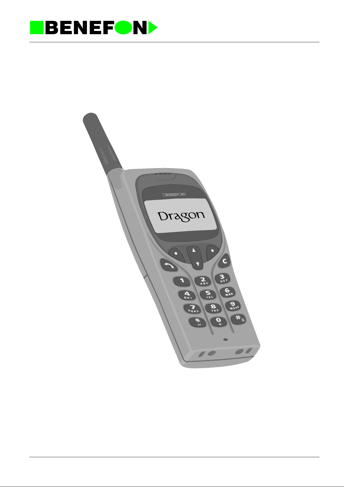
BENEFON DRAGON
TDP70WN
1
Page 2

Product: TDP70WN /
5.9.2000
CONTENTS
1.0 GENERAL . . . . . . . . . . . . . . . . . . . . . . . . . . . . . . . . . . 1 - 1
1.1 TECHNICAL INFORMATION . . . . . . . . . . . . . . . . . . . . . . . . 1 - 1
1.1.1 Operational System . . . . . . . . . . . . . . . . . . . . . . . . . . 1 - 1
1.1.2 Dimensions . . . . . . . . . . . . . . . . . . . . . . . . . . . . . . . . . 1 - 1
1.1.3 Power Consumption . . . . . . . . . . . . . . . . . . . . . . . . . . 1 - 1
1.1.4 Accessories . . . . . . . . . . . . . . . . . . . . . . . . . . . . . . . . . 1 - 1
1.1.5 Alert Functions . . . . . . . . . . . . . . . . . . . . . . . . . . . . . . 1 - 1
1.1.6 Memory . . . . . . . . . . . . . . . . . . . . . . . . . . . . . . . . . . . . 1 - 2
1.1.7 Clock . . . . . . . . . . . . . . . . . . . . . . . . . . . . . . . . . . . . . . 1 - 2
1.1.8 Auto Answer; Pager/Hands Free . . . . . . . . . . . . . . . . 1 - 2
1.1.9 Other Functions . . . . . . . . . . . . . . . . . . . . . . . . . . . . . 1 - 2
1.1.10 Additional Exchange-Based Features . . . . . . . . . . . . 1 - 3
1.1.11 Manufacturer . . . . . . . . . . . . . . . . . . . . . . . . . . . . . . . 1 - 3
1.2 PRODUCT FAMILY . . . . . . . . . . . . . . . . . . . . . . . . . . . . . . . 1 - 4
2.0 OWNER’S MANUAL . . . . . . . . . . . . . . . . . . . . . . . . . . 2 - 1
3.0 INSTALLATION INSTRUCTIONS . . . . . . . . . . . . . . . 3 - 1
3.1 Phone Programming . . . . . . . . . . . . . . . . . . . . . . . . . . . . . . . 3 - 1
3.1.1 Programming Subscriber ID in Dragon . . . . . . . . . . . . 3 - 1
3.1.2 To program Using the Phone Keys . . . . . . . . . . . . . . . 3 - 2
3.1.3 To program Using the BeneLoc Program . . . . . . . . . . 3 - 3
4.0 BeneLoc . . . . . . . . . . . . . . . . . . . . . . . . . . . . . . . . . . . 4 - 1
4.0.1 Installation of BeneLoc program . . . . . . . . . . . . . . . . . 4 - 1
4.0.2 To start the BeneLoc program . . . . . . . . . . . . . . . . . . 4 - 2
5.0 PHONE’S CONSTRUCTION . . . . . . . . . . . . . . . . . . . . 5 - 1
Dp_70ngbTOC.fm
4.0.3 Using the BeneLoc program . . . . . . . . . . . . . . . . . . . . 4 - 3
5.1 PROCESSOR . . . . . . . . . . . . . . . . . . . . . . . . . . . . . . . . . . . . 5 - 2
5.1.1 General . . . . . . . . . . . . . . . . . . . . . . . . . . . . . . . . . . . . 5 - 2
5.1.2 Connectors: . . . . . . . . . . . . . . . . . . . . . . . . . . . . . . . . 5 - 2
5.1.3 Functions . . . . . . . . . . . . . . . . . . . . . . . . . . . . . . . . . . 5 - 4
5.2 AUDIO . . . . . . . . . . . . . . . . . . . . . . . . . . . . . . . . . . . . . . . . . 5 - 7
2
Page 3

Product: TDP70WN /
5.9.2000
5.2.1 Function Description . . . . . . . . . . . . . . . . . . . . . . . . . . 5 - 7
5.2.2 TX-audio . . . . . . . . . . . . . . . . . . . . . . . . . . . . . . . . . . . 5 - 7
5.2.3 RX-Audio . . . . . . . . . . . . . . . . . . . . . . . . . . . . . . . . . . 5 - 8
5.2.4 FII Signal . . . . . . . . . . . . . . . . . . . . . . . . . . . . . . . . . . . 5 - 8
5.2.5 FFSK Modem . . . . . . . . . . . . . . . . . . . . . . . . . . . . . . . 5 - 9
5.2.6 The DTMF Generator/Receiver . . . . . . . . . . . . . . . . . 5 - 9
5.2.7 Signal level detectors . . . . . . . . . . . . . . . . . . . . . . . . . 5 - 9
5.2.8 Compander/Expander . . . . . . . . . . . . . . . . . . . . . . . . 5 - 10
5.2.9 Alarm buzzer . . . . . . . . . . . . . . . . . . . . . . . . . . . . . . . 5 - 10
5.2.10 The other in audio asic (I7) . . . . . . . . . . . . . . . . . . . 5 - 10
5.2.11 Scrambler (optional) . . . . . . . . . . . . . . . . . . . . . . . . 5 - 10
5.3 RX SYNTHESIZER . . . . . . . . . . . . . . . . . . . . . . . . . . . . . . . 5 - 11
5.3.1 General . . . . . . . . . . . . . . . . . . . . . . . . . . . . . . . . . . . 5 - 11
5.3.2 Functional Description . . . . . . . . . . . . . . . . . . . . . . . 5 - 11
5.3.3 Control- and Output-Signals . . . . . . . . . . . . . . . . . . . 5 - 11
5.4 TX-SYNTHESIZER . . . . . . . . . . . . . . . . . . . . . . . . . . . . . . . 5 - 12
5.4.1 General . . . . . . . . . . . . . . . . . . . . . . . . . . . . . . . . . . . 5 - 12
5.4.2 Function Description . . . . . . . . . . . . . . . . . . . . . . . . . 5 - 12
5.4.3 Control- and Output-Signals . . . . . . . . . . . . . . . . . . . 5 - 13
5.5 RECEIVER . . . . . . . . . . . . . . . . . . . . . . . . . . . . . . . . . . . . . 5 - 13
5.5.1 General . . . . . . . . . . . . . . . . . . . . . . . . . . . . . . . . . . . 5 - 13
5.5.2 Input- and Output-Signals . . . . . . . . . . . . . . . . . . . . . 5 - 14
5.6 TRANSMITTER . . . . . . . . . . . . . . . . . . . . . . . . . . . . . . . . . 5 - 15
5.6.1 General . . . . . . . . . . . . . . . . . . . . . . . . . . . . . . . . . . . 5 - 15
5.6.2 Function Description . . . . . . . . . . . . . . . . . . . . . . . . . 5 - 15
5.6.3 Control- and Output-Signals . . . . . . . . . . . . . . . . . . . 5 - 15
5.7 Module OC2285 (The Layout PC2200 A5) . . . . . . . . . . . . . 5 - 18
5.7.1 Parts list . . . . . . . . . . . . . . . . . . . . . . . . . . . . . . . . . . 5 - 18
Dp_70ngbTOC.fm
5.7.2 Layouts . . . . . . . . . . . . . . . . . . . . . . . . . . . . . . . . . . . 5 - 28
5.7.3 Circuit Diagrams . . . . . . . . . . . . . . . . . . . . . . . . . . . . 5 - 30
5.8 Module OC2295 (The Layout PC2200 A5) . . . . . . . . . . . . . 5 - 38
5.8.1 Parts list . . . . . . . . . . . . . . . . . . . . . . . . . . . . . . . . . . 5 - 38
5.8.2 Layouts . . . . . . . . . . . . . . . . . . . . . . . . . . . . . . . . . . . 5 - 48
5.8.3 Circuit Diagrams . . . . . . . . . . . . . . . . . . . . . . . . . . . . 5 - 50
5.9 KEYBOARD OK2200 . . . . . . . . . . . . . . . . . . . . . . . . . . . . . 5 - 58
3
Page 4

1.0 GENERAL
General
1.1 TECHNICAL INFORMATION
1.1.1 Operational System
NMT-450i
1.1.2 Dimensions
Size: 56 x 125 x 25 mm
Weight: 178 g
Product: TDP70WN / General
5.9.2000
Vo lum e: 13 9 cm³
1.1.3 Power Consumption
- Batteries: 3x 1.2 V NiMH
- Sleep current: 600 µA
- Standby current: 43 mA
- Conversation mode, high power: app. 1.1 A
- Conversation mode, low power: app. 0.45 A
Charger:
- automatic 1 h rapid charging for NiMH batteries
- automatic 6 h standard charging for NiMH batteries
1.1.4 Accessories
- light holder
- portable hands free
- mains charger
- cigarette lighter charger
- belt clip
1.1.5 Alert Functions
Adjustable ringing tones
- type
2DP_70GB.fm
1
Page 5

- volume
- progressive or fixed
Silent alert
- short tone and ‘call is coming’ text in the display
1.1.6 Memory
Alphanumeric
- 300 memory locations, 23 characters, 1 6 alphanumeric / memory location
- memory scroll and recall in alphabetical or numerical order
- writing in memory during a call
Repeat: last dialled number or one of 15numbers from the quick-memory locations
Product: TDP70WN / General
5.9.2000
1.1.7 Clock
- time and date display
- real time alarm setting
- real time power on setting
- real time power off setting
- elapsed conversation time counter (both incoming and outgoing)
- received call counter and time display
1.1.8 Auto Answer; Pager/Hands Free
- pre-set number of ring tones before answering (0...6)
Pager
- answers incoming calls and receives numeric messages
- 15memory locations (23 characters / location)
Hands Free
- answers incoming calls when connected to portable HF
1.1.9 Other Functions
DTMF - receiver / transmitter
DTMF - key tones
Display and key illumination
Volume control
2DP_70GB.fm
2
Page 6

Product: TDP70WN / General
5.9.2000
- 5 levels
- level indicator
Battery charge level indicator
- battery empty alarm tone and display
- used battery capacity display
Field strength indicator
Battery-saving function
Prefix editor
Keys lockable to prevent accidental operation
Phone code to prevent una u thorised use
SIS protection function
CLIP, calling line identity presentation
‘+’ international prefix
1.1.10 Additional Exchange-Based Features
Call management
- New call
- Pick incoming call
- Select call
MFT-function (DTMF signal transmission)
Voice privacy (also manual voice privacy)
SMS
1.1.11 Manufacturer
Benefon Oyj
2DP_70GB.fm
P.O. Box 84
24101 Salo
Finland
Tel. +358 2 77400 Fax. +358 2 7332633
3
Page 7

1.2 PRODUCT FAMILY
- BENEFON DRAGON HANDPORTABLE TDP70WN
- STANDARD MAINS CHARGER CSA-70-230
- QUICK MAINS CHARGER CMA-70-230
- CIGARETTE LIGHTER CHARGER CCS-70-12
- LIGHT HOLDER KDC-70
- PORTABL E HAND S FREE EHS-60
- BELT CLIP
Product: TDP70WN / General
5.9.2000
2DP_70GB.fm
4
Page 8

2.0 OWNER’S MANUAL
1user_gb.fm 1
Page 9

Product: TDP70WN / Installation Instructions
5.9.2000
3.0 INSTALLATION INSTRUCTIONS
Installation Instructions
3.1 Phone Programming
You can program Benefon Dragon by using either the keys on your phone, or
the BeneLoc computer program and maintenance adapter. In either case, you
will need a localbox.
Programming Menu Commands:
- SALES DATE
- RADIO PATH ID
- OWN NUMBER
- PHONE CODE
- Y1 Y3 ID (additional operator indicator)
- SW VERSION
- SAK
- PRODUCT CODE
- UPDATE LOCALBOX
- INTERLEAVING
- AUTOMATIC ROAMING
- RESET RAM
3.1.1 Programming Subscriber ID in Dragon
3.1.1.1 How to program the ID in Dragon:
1. Turn on the Dragon normally with its own battery.
2. Hook up the rapid charger until it the phone indicates that it has started
charging.
6DP_70GB.fm
3. Remove the battery and watch that the display shows an empty battery
frame.
4. Hook the localbox adapter up to the localbox via the Spica cable, and then
attach it to the phone where the battery would normally go.
5. Restart the Dragon.
6. You can get to the ***BENEFON*** menu with the arrow key. Select it, and
from there you will find "Radio Path ID", where you can program the ID of the
phone.
1
Page 10

Product: TDP70WN / Installation Instructions
5.9.2000
3.1.2 To program Using the Phone Keys
1. Connect the QPS50 localbox via maintenance adapter to your phone, and
turn the phone on. , will be flashing in the display in stand-by mode.
2. Press and the following text wi ll appear in the displa y: ***BENEFON***.
3.1.2.1 Sales Date
1. Choose SELECT. The following text will appear in the display:
SALES DATE [XXXXXX].
2. Choose CHANGE. [XXXXXX] will be replaced by the date
[daydaymonthmonthyearyear]. Remember to check that the date is correct.
If the date is correct, choose
choosing
daydaymonthmonthyearyear). To save the date, choose
and enter the correct date (six digits in the following form:
SAVE. If the date is incorrect, delete it by
SAVE.
It is possible to program the sales date ONLY ONCE, which means that you
will not be able to change it again afterwards. If the sales date has not been
programmed, your phone will not enter the normal stand-by mode.
3.1.2.2 Radio Path Identification
1. Press , an d the fo llowing text will appear in the display:
RADIO PATH ID [XXXXXXXXXX].
2. Choose
save the identification by choosing
radio path identification is correct.
CHANGE. Enter the radio path identification (ten digits), and
3.1.2.3 Own number
1. Press : own number [+ XXXX...X]
2. Choose CHANGE. Enter the own number (follo w the instruction of the
operator), and save it by choo sing SAVE. Remember to check that the own
number is correct.
Note! SMS doesn’t work if the own number has not been programmed.
SAVE. Remember to check that the
3.1.2.4 Phone Code
1. Press , and the following text will appear in the display:
PHONE CODE [XXXX].
2. Choose CHANGE. Enter the phone code (four digits) , and save th e code
by choosing SAVE.
3.1.2.5 Y1 Y3 ID (Additional operator indicator)
It is possible to change old/add new operator indicator which operates in
automatic roaming mode. (network selection mode: Automatic)
6DP_70GB.fm
2
Page 11
Product: TDP70WN / Installation Instructions
5.9.2000
1. Press : Y1:X Y3:XX ID: ABC
2. Choose SELE CT . Enter Y1 (Country code: one digit) and choose
SAVE.
Enter Y3 (Operator code: two digits) and choose SAVE.
Enter ID (Operator indicator, 3 characters) and choose SAVE.
3.1.2.6 Automatic roaming and Interleaving
The Dealer activates or deactives them according to the operator’s or the
customer’s likings.
3.1.2.7 Closing Instructions
1. Having programmed the necessary information choo se QUIT, and the
following text will appear in the di splay: ***BENEFON***.
2. Turn off your phone, and disconnect the localbox.
3. Turn the phone on once more, and make a test call.
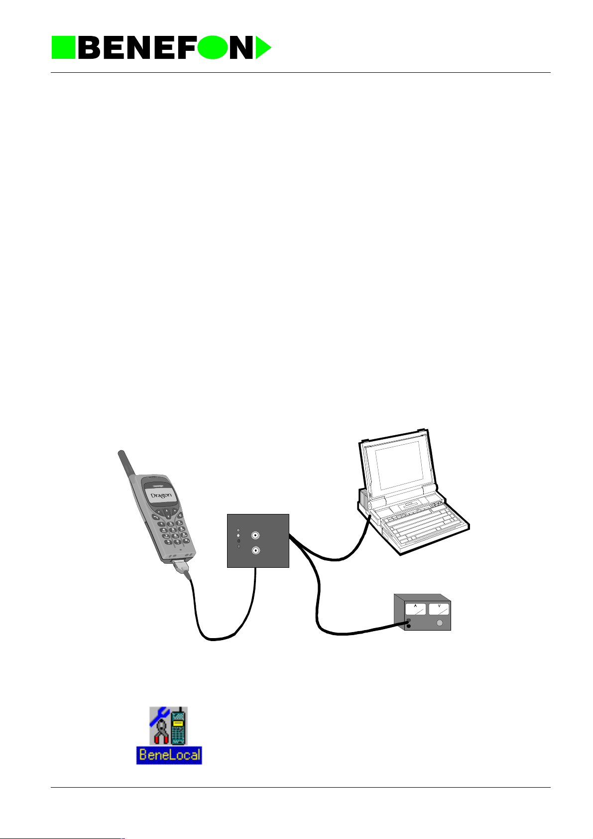
3.1.3 To program Using the BeneLoc Program
power
5V log
gen
flash
5V log
meter
6DP_70GB.fm
Start the installed program by clicking the icon. The phone must be connected
to the system as discribed above.
3
Page 12

Main window
Product: TDP70WN / Installation Instructions
5.9.2000
Press Dealer-key to enter the programming window.
6DP_70GB.fm
You can read the phone data by pressing the Read phone -key. You can
change the miscellanous settings with the computer and transfer them to
phone by pressing the Program phone -key.
BeneLoc includes Help-program for further information.
4
Page 13
4.0 BeneLoc
BeneLoc
Product: TDP70WN / BeneLoc
5.9.2000
power
5V log
gen
flash
5V log
meter
BeneLoc program is desi gned to hel p service person o n tuning and service purp ose.
With Flasher Program you can change the software to Benefon phones.
Both, BeneLoc and Flasher program will need Service Adapter, Power Supply and
Localbox with service rights to work.
4.0.1 Installation of BeneLoc program
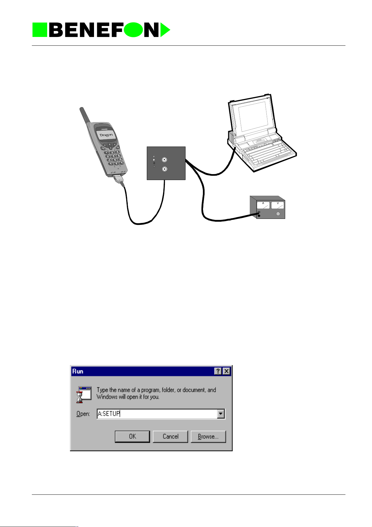
Start Windows. Close all other programs except Program Manager.
Insert BeneLoc Installation Disc 1 in the floppy disk drive of your computer. In the
Program Manager window, choose Run from File menu.
Ty pe the letter A: or B: to indicate your floppy disc drive, and then type SETUP.EXE.
For example, A:\SETUP.EXE.
3dp_70gb
Click the OK button, and follow the instructions displayed on your screen.
The Setup Program will ask you to specify the drive and directory in which you want
1
Page 14

to install the BeneLoc Program. The P r ogram suggests the following: C:\Bene-
App\BeneLoc. Accept the drive and director y by cli cking Next button. You can also
type your own directory for BeneLoc Program .
The Setup Program creates all nec es sary directories and subdirectories to your
computer. Setup Program also creates its own group window in Program Manager.
4.0.2 To start the BeneLoc program
Connect the Servic e Localbox to serial po rt of you r co m put er, which is called COM1
or COM2. The serial ports are usually located in the back of your computer, and
more precise instructions can be found in the manual accompanying the computer.
Adjust the Power Supply voltage to 4.0 Vdc. Connect the Service Localbox to the
Power Supply.
Connect the Servic e Adapter to the phone. Pl ug the cabl e with flat conn ector into the
connector at the bottom of the phone. When the cable has been connected and the
phone is switched on, the phone should be in LOCAL mode. You can test this by
pressing arrow button. There should be ***BENEFON*** on the di splay, if not, clean
connectors and try again. When phone is in LOCAL mode you can start the BeneLoc Program.
Product: TDP70WN / BeneLoc
5.9.2000
To start the BeneLoc Program, double click the BeneLoc icon.
In the BeneLoc Startup window, first sele ct th e correct serial p ort. The n, you ha ve to
select type of the phone. You can also use the Autodetect option. After selection
click OK to start Be neLoc Program. When operating without external power sup ply
the phone may be on sleep m ode an d r egi str a ti on f ai ls . You can wake up the phon e
by pressing some buttons on the phone.
3dp_70gb
2
Page 15

4.0.3 Using the BeneLoc program
In the main window of the BeneLoc, you will find submenus and buttons. Clicking the
buttons you can go to the submenus.
Change
For changing phone to another similar you do not need to do more than enter into
main menu. It means that this button is not needed. If you are going to change the
tested phone to one having different software in, clicking Change will start the registration protocol again.
Product: TDP70WN / BeneLoc
5.9.2000
Help
Dealer
About BeneLoc submenu will tell you version of the BeneLoc Program and also the
state of memory.
About Cellular submenu will show you information of t he phone. Type of phones
software, sales date, date of the software, serial number and present tuning values
of the phone. You can not change the tuning values from Help menu.
From Dealer submenu you can make or check programming of the phone. You will
also find the SIS information from Dealer submenu.
3dp_70gb
3
Page 16

Service
Product: TDP70WN / BeneLoc
5.9.2000
You can control the audio lines (for e xample , switch Rx aud io and com pan der on /off )
in the Service mai n menu . It is al so possible to contro l the ph one to de sired ch annel.
There is also possible to change the power of transmitter.
In the Ports submenu is you can see the status of different digital ports. There is
also possible to control some of the output ports.
You can read the status of the A/D converters from the A/D submen u. Select 8 di ffer ent topics to view. By clicking SCAN AD button The Beneloc will scan A/D the state
of converters continuously. Scanning can stopped by clicking ST OP AD .
Memory submenu allows you to make Ram reset.
By clicking Initialize You can clear all LOCAL settings in service menu.
Home button will return you back to main menu.
Tunings
3dp_70gb
From Tunings main menu you can select different tunings to do. Every tuning have
they own instruction window. Follow given instruc tions to do tunings. Clicking
START will start tuning. The value will be stored only by clicking SAVE. Some of th e
tunings are chained and you can enter to next phase by clicking NEXT.
4
4
Page 17

System
File
Product: TDP70WN / BeneLoc
5.9.2000
You select used mobile phone system from this submenu.
From settings submenu you can manually change settings of the communication
port.
3dp_70gb
5
Page 18

Product: TDP70WN /
5.9.2000
5.0 PHONE’S CONSTRUCTION
7dp_70gb
3
E
2
0
A
0
1
Page 19

LOGIC / AUDIO
OC2285 Processor/Audio/RF
5.1 PROCESSOR
5.1.1 General
The entire radio: The audio, processor and RF functions are found within a
single OC2200 board, along with the display and keyboard.
The processor controls the audio and radio (RF) parts, internal devices and
external accessories.
The µCBIC (processor-asic) includes:
µCBIC IG3010
PROM 29DL800BT Flash program memory
SIS IG2048
Product: TDP70WN / OC2285 Processor/Audio/RF
5.9.2000
H8/300H-cpu, 10k*8 CMOS RAM, 8 A/D, 4 D/A, 48
pcs I/O lines,3 series-interfaces, 2 modem-interfaces,
i2c-interface, frequency counter, realtime clock
Asic for SIS-function, 256k*8 EEPROM + Universal
EEPROM for tuning values
5.1.2 Connectors:
5.1.2.1 Connector for service purposes only
1 V-PROG flash programming voltage 0.5/12 -14 Vdc
2 GEN_OUTPUT rx audio signal output 100 mVrms
3 CHGDET charger detector 0/VCC digital
4 SCL i2c clock 0/VCC digital
5 SDA i2c clock 0/VCC digital
6 TXDO RS232 output 0/VCC digital
7 GEN_INPUT tx audio signal output 200 mVrms
8 RXDO RS232 input 0/VCC digital
5.1.2.2 Headset connector, V2
1 HFMIC microphone signal input 10 mVrms
2 HEADSET headset detector 0/VCC digital
3 HFERP earphone signal output 100 mVr ms
4 GND ground
4Z2200GB.fm
2
Page 20

Product: TDP70WN / OC2285 Processor/Audio/RF
5.9.2000
5.1.2.3 Charger connector, V6
1 Charger voltage 6 ...10 V DC
2 Ground
5.1.2.4 Battery connector, V5
1 Ground
2 VB_unfilter ed 3.6 V
5.1.2.5 Battery identification connector, V4
1 Bat_type_1 0/VB digital
2 Bat_type_2 0/VB digital
5.1.2.6 Display and keyboard connector, V3
1GND
2 KEYIN0 key matrix input 0/VCC
3 KEYIN1 key matrix input 0/VCC
4 KEYIN2 key matrix input 0/VCC
5 KEYIN3 key matrix input 0/VCC
6 KEYIN4 key matrix input 0/VCC
7 KEYOUT0 key matrix output 0/VCC
8 KEYOUT1 key matrix output 0/VCC
9 KEYOUT2 key matrix output 0/VCC
10 KEYOUT3 key matrix output 0/VCC
11 PWRSW key matrix input 0/VCC
12 PWRKEYIN powerkey 0/VCC
13 GND ground
14 VCC LCD power supply VCC
15 RESET reset signal 0/VCC
16 DCS1 display chip select 0/VCC
17 DAO L:control data H:display data 0/VCC
18 DSCL serial clock line for data 0/VCC
19 DSI serial data input 0/VCC
20..31 connected to the voltage components
32 GND ground
4Z2200GB.fm
3
Page 21

5.1.2.7 Circuit Diagram
The processor, audio and RF circuits diagram is split into seven parts. Signals
in the circuit diagrams have been given names, and signals with the same
name are connected between diagrams (<x> = page).
Page 1 of 7 module connector pins
5.1.3 Functions
Product: TDP70WN / OC2285 Processor/Audio/RF
5.9.2000
2 of 7 power supply + display
3 of 7 µCBIC, EPROM, SIS-function
4 of 7 audio parts
5 of 7 synthesizer
6 of 7 receiver
7 of 7 transmitter
5.1.3.1 µ CBIC
I3 is itself a processor-asic circuit. It is comprised H8/300H-cpu, 10k*8 CMOS
RAM, 8 A/D, 4 D/A, 48 pcs I/O lines, 3 series-interfaces, 2 modem-interfaces,
i2c-interface, frequency counter, realtime clock, timers and 4,8 MHz clock
oscillator. The µCBIC divides this by 4 to get timing signal E.
When the process or is operating, RESET = VCC, VCC = 2.8 V, E = 1.2 MHz.
5.1.3.2 Memories
Memory and external I/O-circuit address coding is done with the µCBIC circuit
I3. The circuit options CE, OE and WE are 0-active.
The program memory is in 8 Mbit Flash memory 29DL800.
RAM-memory is 10k*8 CMOS RAM and included in the µCBIC. µCBIC uses its
own power suppl y voltage which i s VRAM a nd is al ways oper ating, eve n when
the radio is in the OFF state.
5.1.3.3 The Modem
The FFSK modem is located in the audio circuit. The modem is connected to
the µCBIC by a series line, input to synchronised port, and transmission is
controlled by an µCBIC series output. The modem gives a 1200 Hz signal
RXCLK and TXCLK to the µCBIC. There is a data detector within the modem,
the speed of which is controlled by C57. The µCBIC A/D converter measures
the level of acceptance from ERPDET line. The same detector also serves to
control HF fu n c ti on.
5.1.3.4 AFC
4Z2200GB.fm
The AFC function is performed by an internal µCBIC frequency counter. A 450
kHz intermediat e frequency is amplified to a square-wave form by Q5. The
4
Page 22

frequency is adjusted by µCBIC D/A 1 signal. This approx. 1.5 Vdc voltage is
fed to the synthesiser AFC pin.
5.1.3.5 Sleep Timer
The phone puts the central functions to sleep for a time. Although everything
seems normal to th e user, but mo st of the fun ctions are closed dow n. The radio
and audio units are closed down completely. The processor still has a power
supply, but the processor is halted and has minimal power consumption. Only
the µCBIC circuit sleep timer and its 32 kHz crystal oscilla tor remain in active
mode. The phone is "woken up" by interrupting the sleep timer or by changing
the keyboard state. Th e sleep time r 32 kHz clock fr eque ncy is pr oduced by the
oscillator made by crystal X1.
5.1.3.6 Warm start
C32 and R38 meas ure th e l en gt h of a voltage break. The vol ta ge dr op s dur i ng
a break, after which it is measured by the A/D (AN2) converter. The time
constant is approx. 10 s. Thus a "warm start" is detected.
Product: TDP70WN / OC2285 Processor/Audio/RF
5.9.2000
5.1.3.7 Reset
The output (VCC) of the main voltage regulator I11 is connected to the power
supply reset monitor I1. The output of I1 resets (stops) the processor and
zeroes the controls when the battery voltage drops below 2.6 V. When the
voltage rises again, the processor restarts.
5.1.3.8 Power Switch
When the power switch is pressed, th e PWRSW line goes to high state and
drives the regulator to operate. The program commences and checks the
PWRSW line to ensure that the switch is being pressed, and sets hold on the
regulator for the PWRON line. Wh en the switch is d ep ressed fo r a lo ng er time,
the program directs power to the PWROFF line. During a short voltage break,
C1 remembers the previous control, i.e. C1 keeps the control voltage high
when the battery voltage is restored within 10 seconds. C1 also serves as a
watch-dog should the voltage drop or processor error-state continue; after 10
seconds, the radio will shut down completely.
Note1! When the phone is operative, the same power power switch acts also
the # key.
Note2! The µCBIC circuits have their own power supply voltage connected to
the battery to e nsu re an u ni nte r rupte d power supply. The µCBIC power su pp ly
is ensured during a battery-back change by the battery B 1.
5.1.3.9 Battery Voltage Measurement
The battery voltage is measured by an A/D converter (AN7). The reference
voltage for the measurement is provided by the main regulator 2.8 V supply.
Calibration is done by the program against a precisely known battery voltage.
4Z2200GB.fm
5
Page 23

5.1.3.10 I/O ports
The µCBIC I/O ports PA PF are 8-bit hold circuits. Data is fed to the addresed
output. When the RESET line is down (0 V) all the µCBIC ports are ze roed (0V).
As RESET rises again, all of th e two-way I/O p orts are inputs un til the prog ram
sets them to the desired state. With the radio in OFF state, RESET is down so
all of the controls are also down although µCBIC is still provided with
operational voltage VRAM.
5.1.3.11 SIS
SIM is performed by a BENEFON ASIC IG2048 manufactured by Atmel.
Integrated circui t IG 20 48 is E2 logic arra y. Th is typ e o f ar ra y i n corpo ra tes bo th
an electrically erasable and programmable read only memory (EEPROM) and
a gate array for SIM function.
SIM has 256 bytes internal EEPROM di vided to tw o part s: 224 byte s EEPROM
for universal use and 32 bytes EEPROM for SIS calculations are secured by
programmable fuse function.
Product: TDP70WN / OC2285 Processor/Audio/RF
5.9.2000
User specific information is stored in EEPROM which CANNOT be read from
outside the chip. All external attemps to read the information clear both.
EEPROM and RAM (fill with FF).
5.1.3.12 Power Adjustment
The transmitter control logic switches TX power and also adjusts it to the
correct level. The TXS_REG signal sets the transmitter to ready mode. Power
is controlled by the µCBIC analog output A/D 0 through the TXPWR line. 0 V
corresponds to "no power" and 2.8 V to maximum transmitter power. The
power levels are calibrated by the program at the source of me asurement.
5.1.3.13 Charging Control
The charger is con trol led by th e pro gram. The char ger is detect ed by a volta ge
at the CHGDET pin. The chargin g curr en t is con tro l led w ith Q10 which acts as
a switch. The switch Q10 is controlled by Q4 through the charge_on -line.
5.1.3.14 Temperature Measurement
The radio has one temperature sensor R72, situated just under the battery
pack. Inside the radio the NTC resisto r R72 voltage is measu red by the µCBIC
A/D converter (AN6). This value is converted by a programmed table to a
temperature reading.
5.1.3.15 Real-time Clock
A real-time clock is pr ovided with in µCBIC to give the ti me and dat e. The alarm
function can also be programmed to the ALARM pin. This will initiate the main
regulator and thus also the radio although it is in OFF state.
4Z2200GB.fm
6
Page 24

The µCBIC circuit has a continuous power supply and th e 3 2 kHz clock crystal
runs constantly. Not even the RESET line stops the clock. If the power supply
has dropped too low, the clock will need to be reset with the radio buttons (from
the menu).
5.2 AUDIO
5.2.1 Function Description
The audio module is comprised of the following functions:
1. TX-audio signal handling
2. RX-audio signal handling
3. Fii signal handling
Product: TDP70WN / OC2285 Processor/Audio/RF
5.9.2000
4. FFSK modem
5. DTMF generator/receiver
6. Signal level detectors
7. Compander
8. Expander
9. Buzzer
The audio functi ons are mainly located in a single circuit AK2339. This chip
from AKM is controlled by a serialbus. It is possible to shut down parts of the
circuit, one block at a time to minimise power consumption.
5.2.2 TX-audio
The input from the microphone is fed to the audio circuit I7 pin 61, which is an
operational amplifier (AMP1) inverting input. The operational amplifier gain is
set by resistor s R87 and R89. The amplifier is connected as a low pass filter.
After the amplifier is th e micr op ho ne sw i tch an d the n sum m ing j un c tion of MIC
input signal, EXTMIC input signal and transmit DTMF signal. VR1 is a
programmable am plifier, which sets the microphone signal (sensitivity) to the
correct level. After VR1 comes band-pass filter f or transmitting the voice signal.
A special scrambler circuit I9 can be mounted between the pins 57/58 and 59
of I7. This device is optional and it is controlled also by the serial interface
circuit. TXDET is the transmit voice signal detection circuit which works as a
full wave rectifier. Next comes ATT1 which is an attenuate circuit to set the
transmit signal level in the HF-mode. COMP is the compressor circuit.
Compress the transmitting signal amplitude with square root law. It can be
bypassed. The linearity is adjustable by the control register CVR. Next is VR2,
4Z2200GB.fm
7
Page 25

normal deviation gain control circuit to set the signal level. The P/E & LIMIT
pre-emphasis circuit and limiting circuit, emphasize the higher frequency
component of the signal in order to improve the signal-to-noise ratio of
modulated signal. This block includes a limiting circuit for signal amplitude in
order to confine the maximum deviation of the transmit modulated signal.
Before TXLPF is the FFSKTX switch. TXLPF is the low pass filter to reject the
higher frequency component on the transmit signal. VR3 is a maximum
deviation gain control circuit to set the transmit signal level. After the VR3
comes switch TXAUDON, which mutes the tx-audio signal using the TXMUTE
control. From the switch, the signal is fed to the summing junction (ADD3) of
the tx-audio signal and Fii-signal. Next comes VR4 gain control circuit to set.
SMF1 is smoothing filter for tx-audio signal. The tx-audio signal is then fed to
the RF-stages.
5.2.3 RX-Audio
Product: TDP70WN / OC2285 Processor/Audio/RF
5.9.2000
The rx-audio signal coming from the receiver through the V103 pin 8 is fed to
the audio circuit I7 pin 23. Inside the circuit, the signal is fed to the operational
amplifier (AMP2) inverting input. The amplifier gain is set by resistors R85 and
R95. The signal i s next passed through an anti-aliasi gn filter. VR5 is a gain
control circuit to set the rx-audio signal to the correct level. Next comes deemphasis (D/E) circuit. Equalize the pre-empassized rx-audio signal. The
signal passes from the D/E through the switch RXAUDON. RXBPF is the bandpass filter for the rx-audio signal. RXDET is the rx-audio signal detection circuit.
This circuit works as a full wave rectifier. After the RXBPF comes I8 which is
the split-switch of audiosignal and then expander circuit (EXP). Expand the rxaudio signal amplitude. It can be bypassed. The linearity is adjustable by the
control register EVR. VR6 is a gain control circuit to set the rx-audio signal to
the correct level. After VR6 comes the RXMUTE switch, which is operated by
the RXMUTE control. ADD4 is the summing junction of the rx-audio signal,
external signal (not used), DTMF signal and transmit signal. VR10 is the
volume control circuit to set the level of ea rphone and extern al earphon es. The
scrambler circuit I9 is optional and it is controlled by the serial interface circuit.
The signal is then fed via R91 to the audio amplifier I10. The amplifier drives
the earphone A4 and by controlling the I10 SE/BTL pin, the signal can be
routed to the HF-connector.
5.2.4 FII Signal
The NMT system uses the FII signal to check the radio path quality. This
approx. 4 kHz signal is split from the rx-audio signal after the VR5 and is
filtered through the band-pass filter (FBPF). VR7 sets the FII signal to the
correct level. Switch FILOOPON can be operated by the FIION control, to be
summed with the tx-audio signal before the VR4.
4Z2200GB.fm
8
Page 26

5.2.5 FFSK Modem
The FFSK data signal from FFSK modulator to be transmitted is passed
through the FFSK low-pass filter and pre-emphasis (FFSKP-EM) to the VR9,
which adjusts its level. The data signal is switched using switch FFSKTXON.
The received data signal is spl it from the rx-audi o signal after th e de-emp hasis
circuit. The data signal is fed through the FFSK band-pass filter to the FFSK
demodulator and FFSK data detector.
FFSK DET block. The block works to judge the FFSK signal existence by
comparing the amplitude of the noise reduced FFSK signal and the provided
detection level standard. Once the detector judges a valid FFSK signal, ’H’
signal is put out on the FFSKDET pin (pin43). The data detector speed is
determined by the external condensator C57.
FFSK DEMOD. To recover 1200 bps receive data and clock from the FFSK
signal.
Product: TDP70WN / OC2285 Processor/Audio/RF
5.9.2000
The modem is connected to the CPU by series lines, the receiver to a
synchronised gate, and transmission is directed to an ASIC series output. The
modem provides a 1200 Hz clock signal RXCLK to the processor and TXCLK
to ASIC.
5.2.6 The DTMF Generator/Receiver
The DTMF generator provides all sixteen standard DTMF tones, and each
individual frequen cy separately. The gene rator is used to pr oduce both key and
alarm tones and enable numeric message transmission during a call.
Key and alarm tones are taken from the generator to switch DTMFRXON and
is summed with the rx -a ud io sig nal. Key tones are connected t o earp hone and
external earphones.
When transmit ting a numeric message, the DTMF tones produced b y the
generator are fed through the VR8, which set the DTMF signal level to the
switch DTMFTXON, and then the signal is summed with the tx-audio signal.
The DTMF receiver takes in numeric messages sent to the phone. The route to
the DTMF receiver splits from the rx-audio signal after the summing junction
ADD4.
5.2.7 Signal level detectors
Audio signal level detectors are required for the HF-function to measure the
transmitted and received audio signal level, and to study the data signal level.
Measurement is done by rectifying the signal, and the resultant DC voltage is
read by a phone’s prosessor A/D conve rter. TX DET is at the tran smission side
detector and RXDET is at the receiver side detector.
4Z2200GB.fm
9
Page 27

5.2.8 Compander/Expander
Compander and expander units are included in audio asic I7 and can be
controlled by registers.
5.2.9 Alarm buzzer
Tones for the internal alarm tones are provided by the DTMF generator. The
internal alarm tones path way is DTMF generator, VR8, switch DTMFRXON,
summing junction ADD4, VR11, AMP5 and buzzer. The buzzer volume is
controlled by t he DA3.
5.2.10 The other in audio asic (I7)
OSC is the main oscillator and clock divider for the prosessor.
CLKBUF is clock buffer generate clock out from main clock.
Product: TDP70WN / OC2285 Processor/Audio/RF
5.9.2000
INTERFACE & DATA REGISTER is a 16 bit address/data serial interface
circuit.
BIAS is bias current generator for amplifiers.
TIMER is an 8 bit timer (not used).
DA1, DA2, DA3 are 8 bit linear DA converters.
5.2.11 Scrambler (optional)
The CD264 I9 is a frequency domain scrambler comp atible with NMT cellular
phone system. It contains separate TX and RX paths for full duplex operation
and operates under µProcessor control via a serial interface. The circuit is
optional.
4Z2200GB.fm
10
Page 28

RF
5.3 RX SYNTHESIZER
5.3.1 General
The RX synthesizer generates an upper side injection frequency for the receiver.
The injection frequency is fed to the receive r ’s first mixer.
Operating voltage 3.0 VDC
Current consumptio n 14 mA
Output level to the receiver +1 dBm
Frequency range 541.450...545.9 25 MHz
5.3.2 Functional Description
Product: TDP70WN / OC2285 Processor/Audio/RF
5.9.2000
The RX injection frequency is generated with a phase locked loop. The VCO produces the injection frequency determined by the control voltage. After the VCO
stage comes the amplifier stage Q430. After the amplifier stage, part of the sign al is
fed to the synthesizer cir cuits I400 divider. The synthesizer circuit co ntains a prescaler, programmable divider, reference frequency divider, and a phase detector.
The synthesizer circuit produces current pulses at output DO1 as controlled by the
phase detector. The current pulses either charge or discharge the loop filter. The
VCO control voltage is derived from the loop filter output.
The synthesizer 12.5kHz reference frequency is made by dividing the 13.00 MHz
signal from the temperature compensated oscillator (TCXO). The series-form signal
which control s the ch anne l fr equen cy come s fro m the proc essor. SDA TA, SCLK and
SLE signals are common to both TX- and RX-synthesizers. A positive pulse in the
SLE line loads the division ratio (corresponding to the frequency of the channel) fed
to the SDATA line, to the synthesizer circuit I400.
5.3.3 Control- and Output-Signals
VRX RX synthesizer operating voltage 3.0 V
SCLK Clock signal for the synthesizer control data
SDATA Synthesize r control data
SLE ENABLE pulse to the synthesizer
RXINJ RX synthesizer output to the receiver +1 dBm
RX_REG Control line for VRX-regulator
4Z2200GB.fm
11
Page 29

5.4 TX-SYNTHESIZER
5.4.1 General
The TX synthesizer generates the final modulated transmission frequency, which is
fed to the transmitter.
Operating voltage 3.0 VDC
Current consumption <30 mA
Output level to the transmitter +6 dBm
Frequency range 453.000...457.475 MHz
5.4.2 Function Description
The TX frequency is generated with a phase locked loop (PLL). The VCO produces
the injection frequency determined by the control voltage, and the VCO also has a
modulation input. After the VCO stage come two amplifier stages Q470 and Q480.
These ensure separation between the VCO and transmitter, and also boost the
injection level sufficiently. Part of the signal is fed from between the amplifier stages
to the synthesizer circuit I400 pre-scaler input Fin2. The synthesizer circuit contains
a pre-scaler, programmable divider, reference frequency divider, and a phase detector.
Product: TDP70WN / OC2285 Processor/Audio/RF
5.9.2000
The synthesizer circuit produces current pulses at output DO2 as a result of the
phase detection. The current pulses either charge or discharge the loop filter condensators. The VCO control voltage is derived from the loop filter output.
The synthesizer 12.5kHz reference frequency is made by dividing the 13.00 MHz
signal from the temperature compensated oscillator (TCXO). The series-form signal
which controls the channel frequency comes from the processor. SDATA and SCLK
signals are co mmon to both TX- and RX -synthesizers. A positive pulse in the SLEline loads the division ratio (corresponding to the TX frequency of the channel) fed to
the SDATA line, to the synthesizer circuit I400.
Modulation is fed to the TX synthesizer TX-AUDIO line. The frequency response is
corrected by the components R455 - R458, C454 and C455. Modulation sensitivity
is set by the resistor R459.
4Z2200GB.fm
12
Page 30

5.4.3 Control- and Output-Signals
VTXS TX synthesizer operating voltage (3.0 V)
TXAUDIO Transmitter audio signal
13MHz 13.00 MHz signal to the receiver circuit.
SCLK Clock signal for synthesizer control data
SDATA Synthesizer control dat a
SLE ENABLE pulse to the synthesizer
TXINJ TX synthesizer output to the transmitter (+6 dBm)
AFC AFC control voltage from AF/LOGIC-board
TXS_REG Control line for VTXS-regulator
5.5 RECEIVER
5.5.1 General
Product: TDP70WN / OC2285 Processor/Audio/RF
5.9.2000
The module contains all FM-receiver functional blocks.
RF-amplifier 3SK284
1. mixer balanced mixer
1. IF-amplifier 3SK284
FM IF system SA 607 includes the following blocks:
2. mixer
IF limiter
quadrature detector
RSSI (received signal strength indicator)
When the RF signal is received it is brought through the duplex filter to the amplifier
stage Q500. The amp lified signal is passed th rough the attenuator to the balanced
mixer.The balanced mixe r is ma de by using discret e components, diode D5 10 and
RF-transformer M510.
The upper side injection frequency is brought from the synthesizer through a small
resistive attenuator to the mixer. The 78.45 MHz intermediate frequency from the
mixer output is fed through the IF- filter X520 to the FM IF-circuit I550.
RX injection frequency 541.450...545.925MHz
4Z2200GB.fm
Injection-level/impedance +1 dBm / 50 ohm
The second inte rmediate-freqency local-oscillator-frequency required by the FM IF-
circuit is generated by multiplying the 13.00 MHz reference-oscillator frequency by
six. The multiplier circuit is made with transistor Q530.
The second intermediate frequency is 450 kHz. The phase-shift required by the
quadrature detector is ma de wit h th e L550 . The dete cted AF-s ignal temp eratur e correction is done in the buffer amplifier stage.
13
Page 31

5.5.2 Input- and Output-Signals
RF input from the duplex filter 463.000...467.475 MHz
RXINJ RX injection signal to the balanced mixer
13MHz
VRX RX operating voltage 3.0V from the regulator
450 kHz Output from 2. IF to the AFC detector
RXAUDIO Receiver audio output 175mVrms
RSSI
SENSITIVITY CHECK
channel RF input SINAD psof.
Product: TDP70WN / OC2285 Processor/Audio/RF
5.9.2000
13.00 MHz signal to the multiplier for the
2.mixer
Received signal strength indicator output
0,5...2V
001 -113 dBm >20 dB
180 -113 dBm >20 dB
4Z2200GB.fm
14
Page 32

5.6 TRANSMITTER
5.6.1 General
Operating voltage 3.5 ... 4.5 v
Current consumptio n mid power max. 1.1 A
Input level from the synthesizer +6 dBm
Output level to the duplex filter mid power 33 dBm (2.0W)
Frequency range 453.000...45 7.4 75 MHz
5.6.2 Function Description
The transmitter unit is comprised of three amplifier stages and two attenuator
stages. The pre-amplifier Q620/Q621 and power module I650 form the transmitter
amplifier chain. The attenuators surrounding the pre-amplifier are included to
enhance the electric separation between the TX synthesizer and the transmitter.
Product: TDP70WN / OC2285 Processor/Audio/RF
5.9.2000
low power max. 0.45 A
low power 24.7 dBm (0.3W)
The operationa l am plifi er I640 and transi stor s Q6 41 a nd Q6 42 se rve a s a pow er re gulator circuit, which adjusts the power level so that the voltage from the transmitter
power detector (D660) and the control voltage TXPWR from the audio/processor
unit are equal.
The negative bias voltage for the power amplifier is generated from the 13 MHz
TCXO signal.
I610 amplifies th e sign al for the sw itche d power suppl y Q610 /D61 0 and is the n reg ulated by the z enerdiode D611.
I600 serves as voltage regulator for pre-amplifier and for the negative voltage
generetor.
Q631 serves as the ON/OFF switch for the output power.
5.6.3 Control- and Output-Signals
VBAT
TXBIAS Power ON/OFF control
TXPWR
TXINJ RF signal from the TX synthesizer +6dBm
TXDUPLEX Transmitter output to the duplex filter
Transmitter operating voltage from the
battery-pack (fused )
Power level control signal from the D/A
converter
0...3V
4Z2200GB.fm
15
Page 33

Product: TDP70WN / OC2285 Processor/Audio/RF
5.9.2000
I
4Z2200GB.fm
16
Page 34

Product: TDP70WN / OC2285 Processor/Audio/RF
5.9.2000
4Z2200GB.fm
17
Page 35

Product: TDP70WN / OC2285_A5
5.9.2000
5.7 Module OC2285 (The Layout PC2200 A5)
OC2285_A5
5.7.1 Parts list
CODE PART DESCRIPT. VALUE MANUF. TYPE
AE0024 A2 Buzzer 10x10x3mm 1,5V/70mA Citizen CHB-03E
AM1840 A3 Electret Condenser micr. with rubber holder ????????? OBG-18S40-C33CEC
AE0023 A4 Dy namic transducer 13,3x2,6 low Z Philips WD00518/32U
AB0039 B1 Lithium battery 3V/50mAh Rayovac BR 1225SM2
CU3106 C1 SMD tantal 10uF / 6V +-20% AVX TAJA106M006R
CF0105 C10 SMD capasitor 1uF 10% 6,3V X5R AVX CM105X5R105K06AT
CG0104 C100 SMD capasitor 100nF/10% 6,3V X5R AVX CM05X5R104K06AH
CG0104 C101 SMD capasitor 100nF/10% 6,3V X5R AVX CM05X5R104K06AH
CU3106 C102 SMD tantal 10uF / 6V +-20% AVX TA JA 106M006R
CH0105 C104 SMD capasitor 1uF /-20/+80%/16V TaiyoYuden EMK212 F105Z00T
CG0101 C105 SMD capasitor X7R 100pF Ò5% Murata
CG0104 C11 SMD capasitor 100nF/10% 6,3V X5R AVX CM05X 5R104K 06AH
CG0104 C12 SMD capasitor 100nF/10% 6,3V X5R AVX CM05X 5R104K 06AH
CG0104 C13 SMD capasitor 100nF/10% 6,3V X5R AVX CM05X 5R104K 06AH
CG0104 C14 SMD capasitor 100nF/10% 6,3V X5R AVX CM05X 5R104K 06AH
CG0104 C15 SMD capasitor 100nF/10% 6,3V X5R AVX CM05X 5R104K 06AH
CF0105 C16 SMD capasitor 1uF 10% 6,3V X5R AVX CM105X5R105K06AT
CG0101 C17 SMD capasitor X7R 100pF Ò5% Murata
CG0220 C18 SMD capasitor NPO 22pF Ò5% Murata
CG0220 C19 SMD capasitor NPO 22pF Ò5% Murata
CG0101 C2 S MD capasitor X7R 100pF Ò5% Murata
CG0223 C20 SMD capasitor X7R 22nF 20% Murata
CG0471 C21 SMD capasitor X7R 470pF Ò10% Mu ra ta
CG0223 C22 SMD capasitor X7R 22nF 20% Murata
CD0105 C23 SMD capasitor 1uF/16V%10% X5R TaiyoYuden EMK212BJ105KG-T
CG0102 C24 SMD capasitor X7R 1nF Ò10% Mur a ta
CF0105 C25 SMD capasitor 1uF 10% 6,3V X5R AVX CM105X5R105K06AT
CH0105 C26 SMD capasitor 1uF/-20/+80%/16V TaiyoYuden EMK212 F105Z00T
CU3106 C27 SMD tantal 10uF / 6V +-20% AVX TAJA106M006R
CG0103 C28 SMD capasitor X7R 10nF Ò10% Murata
CG0472 C29 SMD capasitor X7R 4,7nF/Ò10%/25V AVX
CG0101 C3 S MD capasitor X7R 100pF Ò5% Murata
CG0101 C30 SMD capasitor X7R 100pF Ò5% Murata
CG0223 C31 SMD capasitor X7R 22nF 20% Murata
CU3106 C32 SMD tantal 10uF / 6V +-20% AVX TAJA106M006R
CG0104 C34 SMD capasitor 100nF/10% 6,3V X5R AVX CM05X 5R104K 06AH
CG0104 C35 SMD capasitor 100nF/10% 6,3V X5R AVX CM05X 5R104K 06AH
CG0104 C36 SMD capasitor 100nF/10% 6,3V X5R AVX CM05X 5R104K 06AH
CG0472 C37 SMD capasitor X7R 4,7nF/Ò10%/25V AVX
CG0103 C39 SMD capasitor X7R 10nF Ò10% Murata
CU3106 C4 SMD tantal 10uF / 6V +-20% AVX TAJA106M006R
CG0103 C40 SMD capasitor X7R 10nF Ò10% Murata
CF0223 C400 SMD capasitor 22 nF 10% 50 V X7R Philips
CH0105 C401 SMD capasitor 1uF/-20/+80%/16V TaiyoYuden EMK212 F105Z00T
CH0105 C402 SMD capasitor 1uF/-20/+80%/16V TaiyoYuden EMK212 F105Z00T
CF0223 C403 SMD capasitor 22 nF 10% 50 V X7R Philips
CG0220 C41 SMD capasitor NPO 22pF Ò5% Murata
CD0223 C410 SMD capasitor 22 nF 10% 50 V X7R Philips
CU0334 C411 SMD tantalium capasitor 0.33uF/20V/20% AVX/KYO-
CER
TAJR334M020R
4C2285_A5GB.fm
18
Page 36

Product: TDP70WN / OC2285_A5
5.9.2000
CODE PART DESCRIPT. VALUE MANUF. TYPE
CD0103 C412 SMD capasitor 10 nF 10% 50 V X7R Philips
CF0223 C413 SMD capasitor 22 nF 10% 50 V X7R Philips
CG0220 C42 SMD capasitor NPO 22pF Ò5% Murata
CG0101 C420 SMD capasitor X7R 100pF Ò5% Murata
CG0150 C421 SMD capasitor NPO 15pF Ò5% Mu ra ta
CG0479 C423 SMD capasitor NPO 4. 7pF Ò0 ,2 5 pF Murata
CG0150 C424 SMD capasitor NPO 15pF Ò5% Mu ra ta
CG0120 C425 SMD capasitor NPO 12pF Ò5% Mu ra ta
CG0180 C426 SMD capasitor NPO 18pF Ò5% Mu ra ta
CG0472 C43 SMD capasitor X7R 4,7nF/Ò10%/25V AVX
CG0101 C430 SMD capasitor X7R 100pF Ò5% Murata
CG0223 C431 SMD capasitor X7R 22nF 20% Murata
CG0109 C432 SMD capasitor NPO 1. 0pF Ò0,2 5 pF Murata
CG0479 C433 SMD capasitor NPO 4. 7pF Ò0 ,2 5 pF Murata
CG0101 C434 SMD capasitor X7R 100pF Ò5% Murata
CG0101 C435 SMD capasitor X7R 100pF Ò5% Murata
CU3106 C436 SMD tantal 10uF / 6V +-20% AVX TAJA106M006R
CG0472 C44 SMD capasitor X7R 4,7nF/Ò10%/25V AVX
CG0103 C440 SMD capasitor X7R 10nF Ò10% Murata
CH0105 C441 SMD capasitor 1uF/-20/+80%/16V TaiyoYuden EMK212 F105Z00T
CG0330 C442 SMD capasitor NPO 33pF Ò5% Mu ra ta
CG0101 C443 SMD capasitor X7R 100pF Ò5% Murata
CG0103 C444 SMD capasitor X7R 10nF Ò10% Murata
CG0223 C45 SMD capasitor X7R 22nF 20% Murata
CD0473 C450 SMD capasitor 47 nF 10% 50 V X7R Philips
CU2105 C451 SMD tantal 1uF/10V AVX TAJR105M010R
CD0103 C452 SMD capasitor 10 nF 10% 50 V X7R Philips
CD0223 C453 SMD capasitor 22 nF 10% 50 V X7R Philips
CU0334 C454 SMD tantalium capasitor 0.33uF/20V/20% AVX/KYO-
CER
CU0334 C455 SMD tantalium capasitor 0.33uF/20V/20% AVX/KYO-
CER
CG0101 C456 SMD capasitor X7R 100pF Ò5% Murata
CG0101 C46 SMD capasitor X7R 100pF Ò5% Murata
CG0101 C460 SMD capasitor X7R 100pF Ò5% Murata
CG0220 C461 SMD capasitor NPO 22pF Ò5% Mu ra ta
CG0109 C462 SMD capasitor NPO 1. 0pF Ò0 ,2 5 pF Murata
CG0479 C463 SMD capasitor NPO 4. 7pF Ò0 ,2 5 pF Murata
CG0150 C464 SMD capasitor NPO 15pF Ò5% Mu ra ta
CG0120 C465 SMD capasitor NPO 12pF Ò5% Mu ra ta
CG0390 C466 SMD capasitor NPO 39pF Ò5% Mu ra ta
CH0105 C47 SMD capasitor 1uF/-20/+80%/16V TaiyoYuden EMK212 F105Z00T
CG0101 C470 SMD capasitor X7R 100pF Ò5% Murata
CG0223 C471 SMD capasitor X7R 22nF 20% Murata
CG0109 C472 SMD capasitor NPO 1. 0pF Ò0,2 5 pF Murata
CG0390 C473 SMD capasitor NPO 39pF Ò5% Mu ra ta
CG0101 C474 SMD capasitor X7R 100pF Ò5% Murata
CG0101 C475 SMD capasitor X7R 100pF Ò5% Murata
CU3106 C476 SMD tantal 10uF / 6V +-20% AVX TAJA106M006R
CG0104 C48 SMD capasitor 100nF/10% 6,3V X5R AVX CM05X 5R104K 06AH
CG0101 C480 SMD capasitor X7R 100pF Ò5% Murata
CG0101 C481 SMD capasitor X7R 100pF Ò5% Murata
CG0101 C482 SMD capasitor X7R 100pF Ò5% Murata
CG0109 C483 SMD capasitor NPO 1. 0pF Ò0 ,2 5 pF Murata
CG0229 C484 SMD capasitor NPO 2. 2pF Ò0 ,2 5 pF Murata
CF0105 C49 SMD capasitor 1uF 10% 6,3V X5R AVX CM105X5R105K06AT
CH0105 C490 SMD capasitor 1uF/-20/+80%/16V TaiyoYuden EMK212 F105Z00T
CD0104 C491 SMD capasitor 100 nF 10% 50 V X7R Philips
CU3106 C492 SMD tantal 10uF / 6V +-20% AVX TAJA106M006R
CG0102 C493 SMD capasitor X7R 1nF Ò10% Mu ra ta
TAJR334M020R
TAJR334M020R
4C2285_A5GB.fm
19
Page 37

Product: TDP70WN / OC2285_A5
5.9.2000
CODE PART DESCRIPT. VALUE MANUF. TYPE
CU2105 C494 SMD tantal 1uF/10V AVX TAJR105M010R
CD0104 C495 SMD capasitor 100 nF 10% 50 V X7R Philips
CU3106 C496 SMD tantal 10uF / 6V +-20% AVX TAJA106M006R
CG0102 C497 SMD capasitor X7R 1nF Ò10% Mu ra ta
CU0224 C498 SMD tanlat 0.22uF/20V/10% AVX/KYO-
CER
CG0104 C5 SMD capasitor 100nF/10% 6,3V X5R AVX CM05X5R104K06AH
CG0223 C50 SMD capasitor X7R 22nF 20% Murata
CG0150 C500 SMD capasitor NPO 15pF Ò5% Mu ra ta
CG0180 C501 SMD capasitor NPO 18pF Ò5% Mu ra ta
CG0109 C502 SMD capasitor NPO 1. 0pF Ò0 ,2 5 pF Murata
CG0399 C503 SMD capasitor NPO 3. 9pF Ò0 ,2 5 pF Murata
CG0101 C504 SMD capasitor X7R 100pF Ò5% Murata
CG0180 C505 SMD capasitor NPO 18pF Ò5% Mu ra ta
CG0399 C506 SMD capasitor NPO 3. 9pF Ò0 ,2 5 pF Murata
CG0101 C507 SMD capasitor X7R 100pF Ò5% Murata
CG0101 C508 SMD capasitor X7R 100pF Ò5% Murata
CG0101 C509 SMD capasitor X7R 100pF Ò5% Murata
CG0104 C51 SMD capasitor 100nF/10% 6,3V X5R AVX CM05X 5R104K 06AH
CG0569 C510 SMD capasitor NPO 5. 6pF Ò0 ,2 5 pF Murata
CG0339 C512 SMD capasitor NPO 3. 3pF Ò0 ,2 5 pF Murata
CG0473 C52 SMD capasitor Y5V 47nF/Ò10%/25V AVX
CG0390 C520 SMD capasitor NPO 39pF Ò5% Mu ra ta
CG0150 C521 SMD capasitor NPO 15pF Ò5% Mu ra ta
CG0102 C522 SMD capasitor X7R 1nF Ò10% Mu ra ta
CG0102 C523 SMD capasitor X7R 1nF Ò10% Mu ra ta
CG0689 C524 SMD capasitor NPO 6. 8pF Ò0 ,2 5 pF Murata
CG0399 C525 SMD capasitor NPO 3. 9pF Ò0 ,2 5 pF Murata
CG0101 C526 SMD capasitor X7R 100pF Ò5% Murata
CG0103 C527 SMD capasitor X7R 10nF Ò10% Murata
CG0104 C53 SMD capasitor 100nF/10% 6,3V X5R AVX CM05X 5R104K 06AH
CG0101 C530 SMD capasitor X7R 100pF Ò5% Murata
CG0150 C531 SMD capasitor NPO 15pF Ò5% Mu ra ta
CG0103 C532 SMD capasitor X7R 10nF Ò10% Murata
CG0103 C533 SMD capasitor X7R 10nF Ò10% Murata
CG0102 C534 SMD capasitor X7R 1nF Ò10% Mu ra ta
CG0103 C535 SMD capasitor X7R 10nF Ò10% Murata
CG0150 C536 SMD capasitor NPO 15pF Ò5% Mu ra ta
CG0399 C537 SMD capasitor NPO 3. 9pF Ò0 ,2 5 pF Murata
CG0330 C538 SMD capasitor NPO 33pF Ò5% Mu ra ta
CG0399 C539 SMD capasitor NPO 3. 9pF Ò0 ,2 5 pF Murata
CF0105 C54 SMD capasitor 1uF 10% 6,3V X5R AVX CM105X5R105K06AT
CG0339 C540 SMD capasitor NPO 3. 3pF Ò0,2 5 pF Murata
CG0479 C541 SMD capasitor NPO 4. 7pF Ò0 ,2 5 pF Murata
CF0223 C542 SMD capasitor 22 nF 10% 50 V X7R Philips
CH0105 C55 SMD capasitor 1uF/-20/+80%/16V TaiyoYuden EMK212 F105Z00T
CF0223 C550 SMD capasitor 22 nF 10% 50 V X7R Philips
CF0223 C551 SMD capasitor 22 nF 10% 50 V X7R Philips
CF0223 C552 SMD capasitor 22 nF 10% 50 V X7R Philips
CF0223 C553 SMD capasitor 22 nF 10% 50 V X7R Philips
CF0223 C554 SMD capasitor 22 nF 10% 50 V X7R Philips
CG0100 C555 SMD capasitor NPO 10pF -+0.25pF Murata
CF0223 C556 SMD capasitor 22 nF 10% 50 V X7R Philips
CG0104 C56 SMD capasitor 100nF/10% 6,3V X5R AVX CM05X 5R104K 06AH
CG0103 C560 SMD capasitor X7R 10nF Ò10% Murata
CG0103 C561 SMD capasitor X7R 10nF Ò10% Murata
CU2105 C562 SMD tantal 1uF/10V AVX TAJR105M010R
CG0331 C563 SMD capasitor X7R 330pF Ò10% Mu ra ta
CG0473 C57 SMD capasitor Y5V 47nF/Ò10%/25V AVX
CU3106 C570 SMD tantal 10uF / 6V +-20% AVX TAJA106M006R
TAJR224K020R
4C2285_A5GB.fm
20
Page 38

Product: TDP70WN / OC2285_A5
5.9.2000
CODE PART DESCRIPT. VALUE MANUF. TYPE
CG0102 C571 SMD capasitor X7R 1nF Ò10% Mu ra ta
CF0223 C572 SMD capasitor 22 nF 10% 50 V X7R Philips
CG0104 C58 SMD capasitor 100nF/10% 6,3V X5R AVX CM05X 5R104K 06AH
CG0223 C59 SMD capasitor X7R 22nF 20% Murata
CD0105 C6 SMD capasitor 1uF/16V%10% X5R TaiyoYuden EMK212BJ105KG-T
CG0223 C60 SMD capasitor X7R 22nF 20% Murata
CF0180 C600 SMD capasitor 18 pF 5% 50 V NPO Philips
CG0102 C601 SMD capasitor X7R 1nF Ò10% Mu ra ta
CG0103 C602 SMD capasitor X7R 10nF Ò10% Murata
CD0104 C603 SMD capasitor 100 nF 10% 50 V X7R Philips
CU1105 C604 SMD tantal 1uF/16V AVX TAJR105M016R
CU3106 C605 SMD tantal 10uF / 6V +-20% AVX TAJA106M006R
CG0222 C61 SMD capasitor X7R 2.2nF Ò10% Murata
CG0101 C610 SMD capasitor X7R 100pF Ò5% Murata
CG0103 C611 SMD capasitor X7R 10nF Ò10% Murata
CG0390 C612 SMD capasitor NPO 39pF Ò5% Mu ra ta
CU2105 C613 SMD tantal 1uF/10V AVX TAJR105M010R
CG0103 C614 SMD capasitor X7R 10nF Ò10% Murata
CG0331 C615 SMD capasitor X7R 330pF Ò10% Mu ra ta
CG0103 C616 SMD capasitor X7R 10nF Ò10% Murata
CU2105 C617 SMD tantal 1uF/10V AVX TAJR105M010R
CG0103 C618 SMD capasitor X7R 10nF Ò10% Murata
CU2105 C619 SMD tantal 1uF/10V AVX TAJR105M010R
CG0101 C62 SMD capasitor X7R 100pF Ò5% Murata
CG0101 C620 SMD capasitor X7R 100pF Ò5% Murata
CG0103 C621 SMD capasitor X7R 10nF Ò10% Murata
CG0220 C622 SMD capasitor NPO 22pF Ò5% Mu ra ta
CG0101 C623 SMD capasitor X7R 100pF Ò5% Murata
CG0471 C63 SMD capasitor X7R 470pF Ò10% Mur a ta
CG0471 C64 SMD capasitor X7R 470pF Ò10% Mur a ta
CG0222 C640 SMD capasitor X7R 2.2nF Ò10% Murata
CG0332 C641 SMD capasitor X7R 3.3nF Ò10% Murata
CU2105 C642 SMD tantal 1uF/10V AVX TAJR105M010R
CF0105 C65 SMD capasitor 1uF 10% 6,3V X5R AVX CM105X5R105K06AT
CG0569 C650 SMD capasitor NPO 5. 6pF Ò0,2 5 pF Murata
CU1225 C651 SMD tantal 2.2uF/10V AVX TAJS225M010R
CG0102 C652 SMD capasitor X7R 1nF Ò10% Mu ra ta
CG0102 C653 SMD capasitor X7R 1nF Ò10% Mu ra ta
CU1225 C654 SMD tantal 2.2uF/10V AVX TAJS225M010R
CG0104 C66 SMD capasitor 100nF/10% 6,3V X5R AVX CM05X 5R104K 06AH
CG0101 C660 SMD capasitor X7R 100pF Ò5% Murata
CG0101 C661 SMD capasitor X7R 100pF Ò5% Murata
CG0101 C663 SMD capasitor X7R 100pF Ò5% Murata
CG0104 C67 SMD capasitor 100nF/10% 6,3V X5R AVX CM05X 5R104K 06AH
CG0223 C68 SMD capasitor X7R 22nF 20% Murata
CG0101 C69 SMD capasitor X7R 100pF Ò5% Murata
CG0101 C7 S MD capasitor X7R 100pF Ò5% Murata
CG0104 C70 SMD capasitor 100nF/10% 6,3V X5R AVX CM05X 5R104K 06AH
CG0104 C71 SMD capasitor 100nF/10% 6,3V X5R AVX CM05X 5R104K 06AH
CG0104 C72 SMD capasitor 100nF/10% 6,3V X5R AVX CM05X 5R104K 06AH
CG0104 C73 SMD capasitor 100nF/10% 6,3V X5R AVX CM05X 5R104K 06AH
CG0104 C74 SMD capasitor 100nF/10% 6,3V X5R AVX CM05X 5R104K 06AH
CG0104 C75 SMD capasitor 100nF/10% 6,3V X5R AVX CM05X 5R104K 06AH
CG0104 C76 SMD capasitor 100nF/10% 6,3V X5R AVX CM05X 5R104K 06AH
CG0101 C77 SMD capasitor X7R 100pF Ò5% Murata
CG0103 C78 SMD capasitor X7R 10nF Ò10% Murata
CU3106 C79 SMD tantal 10uF / 6V +-20% AVX TAJA106M006R
CF0105 C8 SMD capasitor 1uF 10% 6,3V X5R AVX CM105X5R105K06AT
CG0104 C80 SMD capasitor 100nF/10% 6,3V X5R AVX CM05X 5R104K 06AH
CG0102 C81 SMD capasitor X7R 1nF Ò10% Mura ta
4C2285_A5GB.fm
21
Page 39

Product: TDP70WN / OC2285_A5
5.9.2000
CODE PART DESCRIPT. VALUE MANUF. TYPE
CG0221 C82 SMD capasitor X7R 220pF Ò10% Mur a ta
CG0103 C83 SMD capasitor X7R 10nF Ò10% Murata
CG0103 C84 SMD capasitor X7R 10nF Ò10% Murata
CG0101 C85 SMD capasitor X7R 100pF Ò5% Murata
CG0104 C86 SMD capasitor 100nF/10% 6,3V X5R AVX CM05X 5R104K 06AH
CG0104 C87 SMD capasitor 100nF/10% 6,3V X5R AVX CM05X 5R104K 06AH
CG0470 C88 SMD capasitor NPO 47pF Ò5% Murata
CC2103 C89 SMD capasitor 10nF 10% 100V X7R AVX 12061C103KAT2A
CF0105 C9 SMD capasitor 1uF 10% 6,3V X5R AVX CM105X5R105K06AT
CG0101 C90 SMD capasitor X7R 100pF Ò5% Murata
CG0101 C91 SMD capasitor X7R 100pF Ò5% Murata
CG0101 C915 SMD capasitor X7R 100pF Ò5% Murata
CG0101 C916 SMD capasitor X7R 100pF Ò5% Murata
CG0102 C92 SMD capasitor X7R 1nF Ò10% Mur a ta
CG0101 C93 SMD capasitor X7R 100pF Ò5% Murata
CG0472 C94 SMD capasitor X7R 4,7nF/Ò10%/25V AVX
CG0101 C95 SMD capasitor X7R 100pF Ò5% Murata
CG0101 C96 SMD capasitor X7R 100pF Ò5% Murata
CU3106 C97 SMD tantal 10uF / 6V +-20% AVX TAJA106M006R
CG0101 C98 SMD capasitor X7R 100pF Ò5% Murata
CG0101 C99 SMD capasitor X7R 100pF Ò5% Murata
DS1070 D1 SMD diode pair 70V/100mA common cathode Philips BAV 70W
DS1070 D2 SMD diode pair 70V/100mA common cathode Philips BAV 70W
DY0016 D3 SMD shottky diode 40V/1,33A VF=0.55V Shindengen M1FS4
DS1070 D32 SMD diode pair 70V/100mA com mon cat hode Philips BAV 70W
DS1070 D4 SMD diode pair 70V/100mA common cathode Philips BAV 70W
DC0229 D420 SMD silicon tuning diode 1V/19pF...4V/11pF Toshiba 1SV229
DC0229 D460 SMD silicon tuning diode 1V/19pF...4V/11pF Toshiba 1SV229
DS0019 D5 SMD diode 100v / 200mA Philips BAS19
DY0071 D510 SMD shottky diode 70V 15mA SGS-
Thomso
DY0384 D610 SMD shottky barrier diod 15V /200mA/ VF=0.35V Toshiba 1SS384-TE85L
DZ3327 D611 SMD zenerdiode 2V7 5% 500mW Temic BZM55C2V7-TR
DY0062 D660 SMD shcottky diode 40V 20mA Siemens BAT 62
AF4300 F1 SMD fuse 3A Littlefuse 0430003.WR
IX5061 I1 Power supply reset monit or/ 2,6V Impala ILC5061M-26
IA0311 I10 Audio amplifier 2-5,5V / 250mW Texas Inst TPA31 1DGN
IR7080 I 11 Regulator 2,85V 100mA/SOT23-5 I mpala ILC7081AIM5-28
IR7062 I 12 Regulator LDO 3,0 V /150mA Impala ILC7062CM-30
IX0826 I13 EL-lamp driver 4,5V / 120V Supertex HV826MG
IG3010 I3 Digital-Asic Hitachi HG71C
IS2335 I400 Dual freg.sy nthesizer PLL+prescaler 1.2GHz NationalSe LMX23352TMX
IR1230 I 490 Regulator 3,0V Toko TK11230BM
IR1230 I 495 Regulator 3,0V Toko TK11230BM
IG2048 I5 SIS ASIC Atmel
IV6070 I550 FM IF-system Philips SA607DK
IM8011 I6 Flash mem ory 8 Mb (512x16/1Mx8) 3V A tmel AT49BV8011-90TI
IR1230 I 600 Regulator 3,0V Toko TK11230BM
IC7S00 I610 2-input NAND SOT-23-5 NationalSe NC7S00M5X
IA2211 I640 Single op. amp. 2,7 - 10V 150mW Texas Inst TLV2211CDBV
IW2391 I650 RF-power amplifier 450MHz-485MHz Iwatsu HAB239B
IX2339 I7 Audio processor CMOS base band pros AsahiKasei AK2339
IC0454 I 8 SMD 2x multip./demultip. Toshiba TC4W53FU-TE 12L
IX0264 I9 Scrambler Compatible with NMT450/900 CML CD264
LC0567 L1 SMD inductors 560uH 10% 3,2x2,5mm Murata LQH3C561K34
LC1224 L420 SMD inductor 220 nH/+- 10% Coilcraft 0805CS-221XKBC
LC1224 L460 SMD inductor 220 nH/+- 10% Coilcraft 0805CS-221XKBC
LC3183 L480 SMD inductor 18n -+2% PANA-
SONIC
LC3472 L500 SMD inductor 4n7 -+2% Panasonic ELJRE4N7ZF2
BAS 70-04
ELJRE18NGF2
4C2285_A5GB.fm
22
Page 40

Product: TDP70WN / OC2285_A5
5.9.2000
CODE PART DESCRIPT. VALUE MANUF. TYPE
LC3682 L501 SMD inductor 6n8 -+2% Panasonic ELJRE6N8ZF2
LC3183 L502 SMD inductor 18n -+2% PANA-
SONIC
LC3183 L503 SMD inductor 18n -+2% PANA-
SONIC
LC3822 L504 SMD inductor 8n2 -+2% Panasonic ELJRE8N2ZF2
LC3273 L510 SMD inductor 27nH -+2% Panasonic ELJRE27NGF2
LC3153 L513 SMD inductor 15n -+2% PANA-
SONIC
LC3334 L520 SMD inductor 330nH +-10% TDK MLF1608DR33K
LC3334 L521 SMD inductor 330nH +-10% TDK MLF1608DR33K
LC3224 L530 SMD inductor 220nH+-10% magnet.shielded TDK MLF1608DR22KT
LC3104 L531 SMD inductor 100nH+-10% magnet.shielded TDK MLF1608DR10KT
LC3334 L540 SMD inductor 330nH +-10% TDK MLF1608DR33K
LI1687 L550 SMD Quad. coil 680uH/180pF 455kHz Toko 303LC-1150
LC3472 L600 SMD inductor 4n7 -+2% Panasonic ELJRE4N7ZF2
LC4106 L610 SMD inductor 10uH -+10% TDK MLF3216E100KT
LC3273 L620 SMD inductor 27nH -+2% Panasonic ELJRE27NGF2
AV2200 M1 Vibra motor SanyoSeimi BF-2175
LT1019 M510 RF-transformer SM-T4 1:1:1, 4,5->600MHz Neosid 00 5532 05
QS1847 Q1 piensignaali yleistransi NPN 100mA/45V hfe=200...450 Philips BC847BW
QF6702 Q10 P-channel MOSFE T Vdss 20V rds 0,2 ohm I&R IRLMS6702
QS0060 Q11 SMD transistor arrey NPN/PNP 100mA/50V Siemens BCR 10PN
QS1847 Q2 piensignaali yleistransi NPN 100mA/45V hfe=200...450 Philips BC847BW
QS1857 Q3 piensignaali yleistransi PNP 100mA/45V hfe=220...470 Philips BC857BW
QS1847 Q4 piensignaali yleistransi NPN 100mA/45V hfe=200...450 Philips BC847BW
QA4867 Q420 SMD RF-transistor NPN G=13dB NF=1.2dB/1GHz Sanyo 2SC4867-4
QA4867 Q430 SMD RF-transistor NPN G=13dB NF=1.2dB/1GHz Sanyo 2SC4867-4
QS1847 Q440 piensignaali yleistransi NPN 100mA/45V hfe=200...450 Philips BC847BW
QA4867 Q460 SMD RF-transistor NPN G=13dB NF=1.2dB/1GHz Sanyo 2SC4867-4
QA4867 Q470 SMD RF-transistor NPN G=13dB NF=1.2dB/1GHz Sanyo 2SC4867-4
QA4867 Q480 SMD RF-transistor NPN G=13dB NF=1.2dB/1GHz Sanyo 2SC4867-4
QS1847 Q5 piensignaali yleistransi NPN 100mA/45V hfe=200...450 Philips BC847BW
QF0320 Q500 SMD Dual FET N-channel Toshiba 3SK320
QF0320 Q520 SMD Dual FET N-channel Toshiba 3SK320
QA4867 Q530 SMD RF-transistor NPN G=13dB NF=1.2dB/1GHz Sanyo 2SC4867-4
QAA193 Q610 SMD RF-transistor 6GHz/300mW F=1.9dB Philips BFR93AW
QA4867 Q620 SMD RF-transistor NPN G=13dB NF=1.2dB/1GHz Sanyo 2SC4867-4
QA4867 Q621 SMD RF-transistor NPN G=13dB NF=1.2dB/1GHz Sanyo 2SC4867-4
QF0138 Q630 N-c hannel fet 50V/0,2A Motorola BSS138LT1
QF9430 Q631 S MD p-channe l MOSFET 20V/4,8A/Rds=0.06 Siliconix Si9430DY
QS1847 Q640 piensignaali yleistransi NPN 100mA/45V hfe=200...450 Philips BC847BW
QS1847 Q641 piensignaali yleistransi NPN 100mA/45V hfe=200...450 Philips BC847BW
QS0031 Q642 SMD transistor PNP 1A/25V Sanyo 2SB1119S-TD
QS1857 Q7 piensignaali yleistransi PNP 100mA/45V hfe=220...470 Philips BC857BW
QS1847 Q8 piensignaali yleistransi NPN 100mA/45V hfe=200...450 Philips BC847BW
QF0200 Q9 N-channel MOSFET 20V/0,73A TEMIC TN0200T
RG0104 R1 S MD resistor 100k 5% 0.063W Kamaya RMC1/16S
RG0104 R10 SMD resistor 100k 5% 0.063W Kamaya RMC1/16S
RG0472 R101 SMD resistor 4k7 5% 0.063W Kamaya RMC1/16S
RG0472 R102 SMD resistor 4k7 5% 0.063W Kamaya RMC1/16S
RG0101 R103 SMD resistor 100R 5% 0.063W Kamaya RMC1/16S
RG0105 R104 SMD resistor 1M0 5% 0.063W Kamaya RMC1/16S
RG0102 R105 SMD resistor 1k0 5% 0.063W Kamaya RMC1/16S
RG0222 R107 SMD resistor 2k2 5% 0.063W Kamaya RMC1/16S
RG0472 R108 SMD resistor 4k7 5% 0.063W Kamaya RMC1/16S
RG0224 R109 SMD resistor 220k 5% 0.063W Kamaya RMC1/16S
RG0102 R11 SMD resistor 1k0 5% 0.063W Kamaya RMC1/16S
RG0105 R110 SMD resistor 1M0 5% 0.063W Kamaya RMC1/16S
RG0105 R111 SMD resistor 1M0 5% 0.063W Kamaya RMC1/16S
ELJRE18NGF2
ELJRE18NGF2
ELJRE15NGF2
4C2285_A5GB.fm
23
Page 41

Product: TDP70WN / OC2285_A5
5.9.2000
CODE PART DESCRIPT. VALUE MANUF. TYPE
RG0102 R12 SMD resistor 1k0 5% 0.063W Kamaya RMC1/16S
RG0103 R13 SMD resistor 10k 5% 0.063W Kamaya RMC1/16S
RG0105 R14 SMD resistor 1M0 5% 0.063W Kamaya RMC1/16S
RG0105 R15 SMD resistor 1M0 5% 0.063W Kamaya RMC1/16S
RG0103 R16 SMD resistor 10k 5% 0.063W Kamaya RMC1/16S
RG0104 R17 SMD resistor 100k 5% 0.063W Kamaya RMC1/16S
RG0224 R18 SMD resistor 220k 5% 0.063W Kamaya RMC1/16S
RG0101 R19 SMD resistor 100R 5% 0.063W Kamaya RMC1/16S
RG0103 R2 S MD resistor 10k 5% 0.063 W Kamaya RMC1/16S
RG0102 R20 SMD resistor 1k0 5% 0.063W Kamaya RMC1/16S
RG0102 R21 SMD resistor 1k0 5% 0.063W Kamaya RMC1/16S
RG0102 R22 SMD resistor 1k0 5% 0.063W Kamaya RMC1/16S
RG0100 R23 SMD resistor 10 R 5% 0.063W Kamaya RMC1/ 16S
RG0564 R24 SMD resistor 560k 5% 0.063W Kamaya RMC1/16S
RG0102 R25 SMD resistor 1k0 5% 0.063W Kamaya RMC1/16S
RG0100 R26 SMD resistor 10 R 5% 0.063W Kamaya RMC1/ 16S
RG0100 R27 SMD resistor 10 R 5% 0.063W Kamaya RMC1/ 16S
RG0102 R28 SMD resistor 1k0 5% 0.063W Kamaya RMC1/16S
RG0104 R29 SMD resistor 100k 5% 0.063W Kamaya RMC1/16S
RG0105 R3 S MD resistor 1M 0 5% 0.063W Kamaya RMC1/16S
RG0823 R30 SMD resistor 82k 5% 0.063W Kamaya RMC1/16S
RG0471 R31 SMD resistor 470R 5% 0.063W Kamaya RMC1/16S
RG0104 R32 SMD resistor 100k 5% 0.063W Kamaya RMC1/16S
RG0104 R33 SMD resistor 100k 5% 0.063W Kamaya RMC1/16S
RG0101 R34 SMD resistor 100R 5% 0.063W Kamaya RMC1/16S
RG0101 R35 SMD resistor 100R 5% 0.063W Kamaya RMC1/16S
RG0223 R36 SMD resistor 22k 5% 0.063W Kamaya RMC1/16S
RF0106 R37 SMD resistor 10 M 5% 0.125 W Kamaya
RG0105 R38 SMD resistor 1M0 5% 0.063W Kamaya RMC1/16S
RG0104 R39 SMD resistor 100k 5% 0.063W Kamaya RMC1/16S
RG0104 R4 S MD resistor 100k 5% 0.063W Kamaya RMC1/16S
RG0104 R40 SMD resistor 100k 5% 0.063W Kamaya RMC1/16S
RG0470 R400 SMD resistor 47R 5% 0.063W Kamaya RMC1/16S
RG0220 R401 SMD resistor 22R 5% 0.063W Kamaya RMC1/16S
RG0220 R402 SMD resistor 22R 5% 0.063W Kamaya RMC1/16S
RG0470 R403 SMD resistor 47R 5% 0.063W Kamaya RMC1/16S
RG0472 R404 SMD resistor 4k7 5% 0.063W Kamaya RMC1/16S
RG0472 R405 SMD resistor 4k7 5% 0.063W Kamaya RMC1/16S
RG0472 R406 SMD resistor 4k7 5% 0.063W Kamaya RMC1/16S
RG0105 R41 SMD resistor 1M0 5% 0.063W Kamaya RMC1/16S
RG0272 R411 SMD resistor 2k7 5% 0.063W Kamaya RMC1/16S
RG0152 R412 SMD resistor 1k5 5% 0.063W Kamaya RMC1/16S
RG0152 R413 SMD resistor 1k5 5% 0.063W Kamaya RMC1/16S
RG0100 R414 SMD resistor 10 R 5% 0.063W Kamaya RMC1/16S
RG0102 R42 SMD resistor 1k0 5% 0.063W Kamaya RMC1/16S
RG0682 R420 SMD resistor 6k8 5% 0.063W Kamaya RMC1/16S
RG0152 R421 SMD resistor 1k5 5% 0.063W Kamaya RMC1/16S
RG0680 R422 SMD resistor 68R 5% 0.063W Kamaya RMC1/16S
RG0224 R43 SMD resistor 220k 5% 0.063W Kamaya RMC1/16S
RG0220 R430 SMD resistor 22R 5% 0.063W Kamaya RMC1/16S
RG0392 R431 SMD resistor 3k9 5% 0.063W Kamaya RMC1/16S
RG0102 R432 SMD resistor 1k0 5% 0.063W Kamaya RMC1/16S
RG0151 R433 SMD resistor 150R 5% 0.063W Kamaya RMC1/16S
RG0151 R434 SMD resistor 150R 5% 0.063W Kamaya RMC1/16S
RG0100 R435 SMD resistor 10 R 5% 0.063W Kamaya RMC1/16S
RG0100 R44 SMD resistor 10 R 5% 0.063W Kamaya RMC1/ 16S
RG0103 R440 SMD resistor 10k 5% 0.063W Kamaya RMC1/16S
RG0100 R441 SMD resistor 10 R 5% 0.063W Kamaya RMC1/16S
RG0473 R442 SMD resistor 47k 5% 0.063W Kamaya RMC1/16S
RG0104 R443 SMD resistor 100k 5% 0.063W Kamaya RMC1/16S
4C2285_A5GB.fm
24
Page 42

Product: TDP70WN / OC2285_A5
5.9.2000
CODE PART DESCRIPT. VALUE MANUF. TYPE
RG0103 R444 SMD resistor 10k 5% 0.063W Kamaya RMC1/16S
RG0104 R45 SMD resistor 100k 5% 0.063W Kamaya RMC1/16S
RG0182 R451 SMD resistor 1k8 5% 0.063W Kamaya RMC1/16S
RG0472 R452 SMD resistor 4k7 5% 0.063W Kamaya RMC1/16S
RG0472 R453 SMD resistor 4k7 5% 0.063W Kamaya RMC1/16S
RG0100 R454 SMD resistor 10 R 5% 0.063W Kamaya RMC1/16S
RG0183 R455 SMD resistor 18k 5% 0.063W Kamaya RMC1/16S
RG0823 R456 SMD resistor 82k 5% 0.063W Kamaya RMC1/16S
RG0103 R457 SMD resistor 10k 5% 0.063W Kamaya RMC1/16S
RG0472 R458 SMD resistor 4k7 5% 0.063W Kamaya RMC1/16S
RG0151 R459 SMD resistor 150R 5% 0.063W Kamaya RMC1/16S
RG0104 R46 SMD resistor 100k 5% 0.063W Kamaya RMC1/16S
RG0822 R460 SMD resistor 8k2 5% 0.063W Kamaya RMC1/16S
RG0182 R461 SMD resistor 1k8 5% 0.063W Kamaya RMC1/16S
RG0101 R462 SMD resistor 100R 5% 0.063W Kamaya RMC1/16S
RG0104 R47 SMD resistor 100k 5% 0.063W Kamaya RMC1/16S
RG0220 R470 SMD resistor 22R 5% 0.063W Kamaya RMC1/16S
RG0392 R471 SMD resistor 3k9 5% 0.063W Kamaya RMC1/16S
RG0102 R472 SMD resistor 1k0 5% 0.063W Kamaya RMC1/16S
RG0101 R473 SMD resistor 100R 5% 0.063W Kamaya RMC1/16S
RG0101 R474 SMD resistor 100R 5% 0.063W Kamaya RMC1/16S
RG0100 R475 SMD resistor 10 R 5% 0.063W Kamaya RMC1/16S
RG0104 R48 SMD resistor 100k 5% 0.063W Kamaya RMC1/16S
RG0182 R480 SMD resistor 1k8 5% 0.063W Kamaya RMC1/16S
RG0392 R481 SMD resistor 3k9 5% 0.063W Kamaya RMC1/16S
RG0220 R482 SMD resistor 22R 5% 0.063W Kamaya RMC1/16S
RG0100 R483 SMD resistor 10 R 5% 0.063W Kamaya RMC1/16S
RG0221 R484 SMD resistor 220R 5% 0.063W Kamaya RMC1/16S
RG0104 R49 SMD resistor 100k 5% 0.063W Kamaya RMC1/16S
RG0473 R493 SMD resistor 47k 5% 0.063W Kamaya RMC1/16S
RG0473 R497 SMD resistor 47k 5% 0.063W Kamaya RMC1/16S
RG0103 R5 S MD resistor 10k 5% 0.063 W Kamaya RMC1/16S
RG0102 R50 SMD resistor 1k0 5% 0.063W Kamaya RMC1/16S
RG0680 R501 SMD resistor 68R 5% 0.063W Kamaya RMC1/16S
RG0561 R502 SMD resistor 560R 5% 0.063W Kamaya RMC1/16S
RG0100 R503 SMD resistor 10 R 5% 0.063W Kamaya RMC1/16S
RG0103 R506 SMD resistor 10k 5% 0.063W Kamaya RMC1/16S
RG0333 R507 SMD resistor 33k 5% 0.063W Kamaya RMC1/16S
RG0103 R51 SMD resistor 10k 5% 0.063W Kamaya RMC1/16S
RG0271 R510 SMD resistor 270R 5% 0.063W Kamaya RMC1/16S
RG0180 R511 SMD resistor 18R 5% 0.063W Kamaya RMC1/16S
RG0271 R512 SMD resistor 270R 5% 0.063W Kamaya RMC1/16S
RG0103 R513 SMD resistor 10k 5% 0.063W Kamaya RMC1/16S
RG0101 R52 SMD resistor 100R 5% 0.063W Kamaya RMC1/16S
RG0220 R520 SMD resistor 22R 5% 0.063W Kamaya RMC1/16S
RG0472 R521 SMD resistor 4k7 5% 0.063W Kamaya RMC1/16S
RG0102 R522 SMD resistor 1k0 5% 0.063W Kamaya RMC1/16S
RG0471 R523 SMD resistor 470R 5% 0.063W Kamaya RMC1/16S
RG0103 R53 SMD resistor 10k 5% 0.063W Kamaya RMC1/16S
RG0100 R530 SMD resistor 10 R 5% 0.063W Kamaya RMC1/16S
RG0333 R531 SMD resistor 33k 5% 0.063W Kamaya RMC1/16S
RG0473 R532 SMD resistor 47k 5% 0.063W Kamaya RMC1/16S
RG0471 R533 SMD resistor 470R 5% 0.063W Kamaya RMC1/16S
RG0104 R54 SMD resistor 100k 5% 0.063W Kamaya RMC1/16S
RG0472 R540 SMD resistor 4k7 5% 0.063W Kamaya RMC1/16S
RG0104 R55 SMD resistor 100k 5% 0.063W Kamaya RMC1/16S
RG0272 R550 SMD resistor 2k7 5% 0.063W Kamaya RMC1/16S
RG0102 R551 SMD resistor 1k0 5% 0.063W Kamaya RMC1/16S
RG0222 R552 SMD resistor 2k2 5% 0.063W Kamaya RMC1/16S
RG0332 R553 SMD resistor 3k3 5% 0.063W Kamaya RMC1/16S
4C2285_A5GB.fm
25
Page 43

Product: TDP70WN / OC2285_A5
5.9.2000
CODE PART DESCRIPT. VALUE MANUF. TYPE
RG0333 R554 SMD resistor 33k 5% 0.063W Kamaya RMC1/16S
RG0101 R56 SMD resistor 100R 5% 0.063W Kamaya RMC1/16S
RG0393 R560 SMD resistor 39k 5% 0.063W Kamaya RMC1/16S
RG0683 R561 SMD resistor 68k 5% 0.063W Kamaya RMC1/16S
RTN157 R562 (RNT157)NTC resistor 22k 5% B=3750 Ohizumi 157-223-65001
RG0102 R563 SMD resistor 1k0 5% 0.063W Kamaya RMC1/16S
RG0682 R564 SMD resistor 6k8 5% 0.063W Kamaya RMC1/16S
RG0473 R565 SMD resistor 47k 5% 0.063W Kamaya RMC1/16S
RG0683 R567 SMD resistor 68k 5% 0.063W Kamaya RMC1/16S
RG0333 R568 SMD resistor 33k 5% 0.063W Kamaya RMC1/16S
RG0222 R569 SMD resistor 2k2 5% 0.063W Kamaya RMC1/16S
RG0105 R57 SMD resistor 1M0 5% 0.063W Kamaya RMC1/16S
RG0220 R570 SMD resistor 22R 5% 0.063W Kamaya RMC1/16S
RG0105 R58 SMD resistor 1M0 5% 0.063W Kamaya RMC1/16S
RG0102 R59 SMD resistor 1k0 5% 0.063W Kamaya RMC1/16S
RG0103 R6 S MD resistor 10k 5% 0.063 W Kamaya RMC1/16S
RG0102 R60 SMD resistor 1k0 5% 0.063W Kamaya RMC1/16S
RG0473 R600 SMD resistor 47k 5% 0.063W Kamaya RMC1/16S
RG0102 R605 SMD resistor 1k0 5% 0.063W Kamaya RMC1/16S
RG0102 R61 SMD resistor 1k0 5% 0.063W Kamaya RMC1/16S
RG0100 R610 SMD resistor 10 R 5% 0.063W Kamaya RMC1/16S
RG0105 R611 SMD resistor 1M0 5% 0.063W Kamaya RMC1/16S
RG0102 R612 SMD resistor 1k0 5% 0.063W Kamaya RMC1/16S
RG0151 R613 SMD resistor 150R 5% 0.063W Kamaya RMC1/16S
RG0220 R614 SMD resistor 22R 5% 0.063W Kamaya RMC1/16S
RG0102 R62 SMD resistor 1k0 5% 0.063W Kamaya RMC1/16S
RG0220 R620 SMD resistor 22R 5% 0.063W Kamaya RMC1/16S
RG0101 R621 SMD resistor 100R 5% 0.063W Kamaya RMC1/16S
RG0821 R622 SMD resistor 820R 5% 0.063W Kamaya RMC1/16S
RG0222 R623 SMD resistor 2k2 5% 0.063W Kamaya RMC1/16S
RG0222 R624 SMD resistor 2k2 5% 0.063W Kamaya RMC1/16S
RG0222 R625 SMD resistor 2k2 5% 0.063W Kamaya RMC1/16S
RG0100 R626 SMD resistor 10 R 5% 0.063W Kamaya RMC1/16S
RG0105 R63 SMD resistor 1M0 5% 0.063W Kamaya RMC1/16S
RG0103 R630 SMD resistor 10k 5% 0.063W Kamaya RMC1/16S
RG0224 R631 SMD resistor 220k 5% 0.063W Kamaya RMC1/16S
RG0224 R632 SMD resistor 220k 5% 0.063W Kamaya RMC1/16S
RG0103 R64 SMD resistor 10k 5% 0.063W Kamaya RMC1/16S
RG0224 R640 SMD resistor 220k 5% 0.063W Kamaya RMC1/16S
RG0332 R641 SMD resistor 3k3 5% 0.063W Kamaya RMC1/16S
RG0102 R642 SMD resistor 1k0 5% 0.063W Kamaya RMC1/16S
RG0271 R643 SMD resistor 270R 5% 0.063W Kamaya RMC1/16S
RG0271 R644 SMD resistor 270R 5% 0.063W Kamaya RMC1/16S
RG0104 R65 SMD resistor 100k 5% 0.063W Kamaya RMC1/16S
RG0391 R650 SMD resistor 390R 5% 0.063W Kamaya RMC1/16S
RG0100 R651 SMD resistor 10 R 5% 0.063W Kamaya RMC1/16S
RG0391 R652 SMD resistor 390R 5% 0.063W Kamaya RMC1/16S
RG0103 R660 SMD resistor 10k 5% 0.063W Kamaya RMC1/16S
RG0184 R661 SMD resistor 180k 5% 0.063W Kamaya RMC1/16S
RG0103 R662 SMD resistor 10k 5% 0.063W Kamaya RMC1/16S
RG0104 R663 SMD resistor 100k 5% 0.063W Kamaya RMC1/16S
RG0102 R67 SMD resistor 1k0 5% 0.063W Kamaya RMC1/16S
RG0101 R68 SMD resistor 100R 5% 0.063W Kamaya RMC1/16S
RG0102 R69 SMD resistor 1k0 5% 0.063W Kamaya RMC1/16S
RG0334 R7 S MD resistor 330k 5% 0.063W Kamaya RMC1/16S
RG0103 R70 SMD resistor 10k 5% 0.063W Kamaya RMC1/16S
RG0473 R71 SMD resistor 47k 5% 0.063W Kamaya RMC1/16S
RTN154 R72 SMD NTC-resistor 150k 5% B=4100 Hokuriku 157-154-4500 1TP
RG0104 R73 SMD resistor 100k 5% 0.063W Kamaya RMC1/16S
RG0104 R74 SMD resistor 100k 5% 0.063W Kamaya RMC1/16S
4C2285_A5GB.fm
26
Page 44

Product: TDP70WN / OC2285_A5
5.9.2000
CODE PART DESCRIPT. VALUE MANUF. TYPE
RG0101 R75 SMD resistor 100R 5% 0.063W Kamaya RMC1/16S
RG0105 R76 SMD resistor 1M0 5% 0.063W Kamaya RMC1/16S
RG0104 R77 SMD resistor 100k 5% 0.063W Kamaya RMC1/16S
RG0100 R79 SMD resistor 10 R 5% 0.063W Kamaya RMC1/ 16S
RG0102 R8 S MD resistor 1k0 5% 0.063 W Kamaya RMC1/16S
RG0101 R80 SMD resistor 100R 5% 0.063W Kamaya RMC1/16S
RG0563 R81 SMD resistor 56k 5% 0.063W Kamaya RMC1/16S
RG0222 R82 SMD resistor 2k2 5% 0.063W Kamaya RMC1/16S
RG0102 R83 SMD resistor 1k0 5% 0.063W Kamaya RMC1/16S
RG0563 R84 SMD resistor 56k 5% 0.063W Kamaya RMC1/16S
RG0563 R85 SMD resistor 56k 5% 0.063W Kamaya RMC1/16S
RG0563 R86 SMD resistor 56k 5% 0.063W Kamaya RMC1/16S
RG0153 R87 SMD resistor 15k 5% 0.063W Kamaya RMC1/16S
RG0153 R88 SMD resistor 15k 5% 0.063W Kamaya RMC1/16S
RG0274 R89 SMD resistor 270k 5% 0.063W Kamaya RMC1/16S
RG0103 R9 S MD resistor 10k 5% 0.063 W Kamaya RMC1/16S
RG0223 R90 SMD resistor 22k 5% 0.063W Kamaya RMC1/16S
RG0393 R91 SMD resistor 39k 5% 0.063W Kamaya RMC1/16S
RG0104 R92 SMD resistor 100k 5% 0.063W Kamaya RMC1/16S
RG0103 R93 SMD resistor 10k 5% 0.063W Kamaya RMC1/16S
RG0563 R94 SMD resistor 56k 5% 0.063W Kamaya RMC1/16S
RG0563 R95 SMD resistor 56k 5% 0.063W Kamaya RMC1/16S
RG0104 R96 SMD resistor 100k 5% 0.063W Kamaya RMC1/16S
RG0104 R97 SMD resistor 100k 5% 0.063W Kamaya RMC1/16S
RG0104 R98 SMD resistor 100k 5% 0.063W Kamaya RMC1/16S
RG0224 R99 SMD resistor 220k 5% 0.063W Kamaya RMC1/16S
VN0009 V2 Stereo jack 2,5mm miniature Hosiden HSJ1603-010020
VW0109 V3 Connec tor 32-pin 1mm pitch Elco 589158032000011
VM0002 V4 Modulat cntact 2pin 2A/pin Bours 70AAJ002M0
VM0002 V5 Modulat cntact 2pin 2A/pin Bours 70AAJ002M0
VW0111 V 6 DC -jack 3,5 x 1,0 mm Elka Ltd AJ23 2 - SMT
VR0248 V902 SMA connector ????????? 982589
X32766 X1 SMD crystal 32.768kHz +-30ppm MicroCryst MS1V-TK
X48007 X2 SMD crystal 4,8MHz CL=16pF 30ppm Citezen CS 20
LF0062 X3 SMD EM I filter 10nF/2A Panasonic ELKE103FA
LF0062 X4 SMD EM I filter 10nF/2A Panasonic ELKE103FA
XR1650 X420 Ceramic coaxial resonato 650MHz 4x4x13mm Q>250 Siemens B69614-G0655-B42
XO5130 X440 VCTCXO 13.0 MHz TEW TTS10V
XR1550 X460 Ceramic coaxial resonato 550MHz 4x4x14,5mm Q>250 Siemens B69614-G0550-BA4
XF7845 X520 Crystal filter 78.45MHz 7x5x1.35mm TEW MF78R
XC3450 X550 Ceramic IF-filter 450Khz Murata CFUCG450E
XC4450 X551 Ceramic IF-filter 450kHz M urata CFUCG450F
XI0005 X650 Directional coupler NMT450 MKT Taisei DCS3120-09
LF0062 X901 SMD EMI filter 10nF/2A Panasonic ELKE103FA
OD1085 X902 Duplexer PL Rx463/Tx453MHz LK-Product S2-A9/NP1.0
PC2200 Y254 PCB for OC2200 Elprintta
Last
update
14.08.00
4C2285_A5GB.fm
27
Page 45

5.7.2 Layouts
Product: TDP70WN / OC2285_A5
5.9.2000
4C2285_A5GB.fm
28
Page 46

Product: TDP70WN / OC2285_A5
5.9.2000
4C2285_A5GB.fm
29
Page 47

5.7.3 Circuit Diagrams
Product: TDP70WN / OC2285_A5
5.9.2000
4C2285_A5GB.fm
30
Page 48

Product: TDP70WN / OC2285_A5
5.9.2000
4C2285_A5GB.fm
31
Page 49

Product: TDP70WN / OC2285_A5
5.9.2000
4C2285_A5GB.fm
32
Page 50

Product: TDP70WN / OC2285_A5
5.9.2000
4C2285_A5GB.fm
33
Page 51

Product: TDP70WN / OC2285_A5
5.9.2000
4C2285_A5GB.fm
34
Page 52

Product: TDP70WN / OC2285_A5
5.9.2000
4C2285_A5GB.fm
35
Page 53

Product: TDP70WN / OC2285_A5
5.9.2000
4C2285_A5GB.fm
36
Page 54

Product: TDP70WN / OC2285_A5
5.9.2000
4C2285_A5GB.fm
37
Page 55

Product: TDP70WN / OC2295_A5
5.9.2000
5.8 Module OC2295 (The Layout PC2200 A5)
OC2295_A5
5.8.1 Parts list
CODE PART DESCRIPT. VALUE MANUF. TYPE
AE0024 A2 Buzzer 10x10x3mm 1,5V/70mA Citizen CHB-03E
AM1840 A3 Electret Condenser micr. with rubber holder ????????? OBG-18S40-C33CEC
AE0023 A4 Dy namic transducer 13,3x2,6 low Z Philips WD00518/32U
AB0039 B1 Lithium battery 3V/50mAh Rayovac BR 1225SM2
CU3106 C1 SMD tantal 10uF / 6V +-20% AVX TAJA106M006R
CF0105 C10 SMD capasitor 1uF 10% 6,3V X5R AVX CM105X5R105K06AT
CG0104 C100 SMD capasitor 100nF/10% 6,3V X5R AVX CM05X5R104K06AH
CG0104 C101 SMD capasitor 100nF/10% 6,3V X5R AVX CM05X5R104K06AH
CU3106 C102 SMD tantal 10uF / 6V +-20% AVX TAJA106M006R
CG0104 C103 SMD capasitor 100nF/10% 6,3V X5R AVX CM05X5R104K06AH
CH0105 C104 SMD capasitor 1uF/-20/+80%/16V TaiyoYuden EMK212 F105Z00T
CG0101 C105 SMD capasitor X7R 100pF 5% Murata
CG0104 C11 SMD capasitor 100nF/10% 6,3V X5R AVX CM05X 5R104K 06AH
CG0104 C12 SMD capasitor 100nF/10% 6,3V X5R AVX CM05X 5R104K 06AH
CG0104 C13 SMD capasitor 100nF/10% 6,3V X5R AVX CM05X 5R104K 06AH
CG0104 C14 SMD capasitor 100nF/10% 6,3V X5R AVX CM05X 5R104K 06AH
CG0104 C15 SMD capasitor 100nF/10% 6,3V X5R AVX CM05X 5R104K 06AH
CF0105 C16 SMD capasitor 1uF 10% 6,3V X5R AVX CM105X5R105K06AT
CG0101 C17 SMD capasitor X7R 100pF 5% Murata
CG0220 C18 SMD capasitor NPO 22pF 5% M urata
CG0220 C19 SMD capasitor NPO 22pF 5% M urata
CG0101 C2 S MD capasitor X7R 100pF 5% Murata
CG0223 C20 SMD capasitor X7R 22nF 20% Murata
CG0471 C21 SMD capasitor X7R 470pF 10% Murata
CG0223 C22 SMD capasitor X7R 22nF 20% Murata
CD0105 C23 SMD capasitor 1uF/16V%10% X5R TaiyoYuden EM K212B J105K G- T
CG0102 C24 SMD capasitor X7R 1nF 10% Murata
CF0105 C25 SMD capasitor 1uF 10% 6,3V X5R AVX CM105X5R105K06AT
CH0105 C26 SMD capasitor 1uF/-20/+80%/16V TaiyoYuden EMK212 F105Z00T
CU3106 C27 SMD tantal 10uF / 6V +-20% AVX TAJA106M006R
CG0103 C28 SMD capasitor X7R 10nF 10% Murata
CG0472 C29 SMD capasitor X7R 4,7nF/10%/25V AVX
CG0101 C3 S MD capasitor X7R 100pF 5% Murata
CG0101 C30 SMD capasitor X7R 100pF 5% Murata
CG0223 C31 SMD capasitor X7R 22nF 20% Murata
CU3106 C32 SMD tantal 10uF / 6V +-20% AVX TAJA106M006R
CG0104 C34 SMD capasitor 100nF/10% 6,3V X5R AVX CM05X 5R104K 06AH
CG0104 C35 SMD capasitor 100nF/10% 6,3V X5R AVX CM05X 5R104K 06AH
CG0104 C36 SMD capasitor 100nF/10% 6,3V X5R AVX CM05X 5R104K 06AH
CG0472 C37 SMD capasitor X7R 4,7nF/10%/25V AVX
CG0103 C39 SMD capasitor X7R 10nF 10% Murata
CU3106 C4 SMD tantal 10uF / 6V +-20% AVX TAJA106M006R
CG0103 C40 SMD capasitor X7R 10nF 10% Murata
CF0223 C400 SMD capasitor 22 nF 10% 50 V X7R Philips
CH0105 C401 SMD capasitor 1uF/-20/+80%/16V TaiyoYuden EMK212 F105Z00T
CH0105 C402 SMD capasitor 1uF/-20/+80%/16V TaiyoYuden EMK212 F105Z00T
CF0223 C403 SMD capasitor 22 nF 10% 50 V X7R Philips
CG0220 C41 SMD capasitor NPO 22pF 5% M urata
CD0223 C410 SMD capasitor 22 nF 10% 50 V X7R Philips
4C2295_A5GB.fm
38
Page 56

Product: TDP70WN / OC2295_A5
5.9.2000
CODE PART DESCRIPT. VALUE MANUF. TYPE
CU0334 C411 SMD tantalium capasitor 0.33uF/20V/20% AVX/KYO-
CER
CD0103 C412 SMD capasitor 10 nF 10% 50 V X7R Philips
CF0223 C413 SMD capasitor 22 nF 10% 50 V X7R Philips
CG0220 C42 SMD capasitor NPO 22pF 5% M urata
CG0101 C420 SMD capasitor X7R 100pF 5% Murata
CG0150 C421 SMD capasitor NPO 15pF 5% Murata
CG0479 C423 SMD capasitor NPO 4. 7pF 0,25pF Murata
CG0150 C424 SMD capasitor NPO 15pF 5% Murata
CG0120 C425 SMD capasitor NPO 12pF 5% Murata
CG0180 C426 SMD capasitor NPO 18pF 5% Murata
CG0472 C43 SMD capasitor X7R 4,7nF/10%/25V AVX
CG0101 C430 SMD capasitor X7R 100pF 5% Murata
CG0223 C431 SMD capasitor X7R 22nF 20% Murata
CG0109 C432 SMD capasitor NPO 1. 0pF 0,25pF Murata
CG0479 C433 SMD capasitor NPO 4. 7pF 0,25pF Murata
CG0101 C434 SMD capasitor X7R 100pF 5% Murata
CG0101 C435 SMD capasitor X7R 100pF 5% Murata
CU3106 C436 SMD tantal 10uF / 6V +-20% AVX TAJA106M006R
CG0472 C44 SMD capasitor X7R 4,7nF/10%/25V AVX
CG0103 C440 SMD capasitor X7R 10nF 10% Murata
CH0105 C441 SMD capasitor 1uF/-20/+80%/16V TaiyoYuden EMK212 F105Z00T
CG0330 C442 SMD capasitor NPO 33pF 5% Murata
CG0101 C443 SMD capasitor X7R 100pF 5% Murata
CG0103 C444 SMD capasitor X7R 10nF 10% Murata
CG0223 C45 SMD capasitor X7R 22nF 20% Murata
CD0473 C450 SMD capasitor 47 nF 10% 50 V X7R Philips
CU2105 C451 SMD tantal 1uF/10V AVX TAJR105M010R
CD0103 C452 SMD capasitor 10 nF 10% 50 V X7R Philips
CD0223 C453 SMD capasitor 22 nF 10% 50 V X7R Philips
CU0334 C454 SMD tantalium capasitor 0.33uF/20V/20% AVX/KYO-
CER
CU0334 C455 SMD tantalium capasitor 0.33uF/20V/20% AVX/KYO-
CER
CG0101 C456 SMD capasitor X7R 100pF 5% Murata
CG0101 C46 SMD capasitor X7R 100pF 5% Murata
CG0101 C460 SMD capasitor X7R 100pF 5% Murata
CG0220 C461 SMD capasitor NPO 22pF 5% Murata
CG0109 C462 SMD capasitor NPO 1. 0pF 0,25pF Murata
CG0479 C463 SMD capasitor NPO 4. 7pF 0,25pF Murata
CG0150 C464 SMD capasitor NPO 15pF 5% Murata
CG0120 C465 SMD capasitor NPO 12pF 5% Murata
CG0390 C466 SMD capasitor NPO 39pF 5% Murata
CH0105 C47 SMD capasitor 1uF/-20/+80%/16V TaiyoYuden EMK212 F105Z00T
CG0101 C470 SMD capasitor X7R 100pF 5% Murata
CG0223 C471 SMD capasitor X7R 22nF 20% Murata
CG0109 C472 SMD capasitor NPO 1. 0pF 0,25pF Murata
CG0390 C473 SMD capasitor NPO 39pF 5% Murata
CG0101 C474 SMD capasitor X7R 100pF 5% Murata
CG0101 C475 SMD capasitor X7R 100pF 5% Murata
CU3106 C476 SMD tantal 10uF / 6V +-20% AVX TAJA106M006R
CG0104 C48 SMD capasitor 100nF/10% 6,3V X5R AVX CM05X 5R104K 06AH
CG0101 C480 SMD capasitor X7R 100pF 5% Murata
CG0101 C481 SMD capasitor X7R 100pF 5% Murata
CG0101 C482 SMD capasitor X7R 100pF 5% Murata
CG0109 C483 SMD capasitor NPO 1. 0pF 0,25pF Murata
CG0229 C484 SMD capasitor NPO 2. 2pF 0,25pF Murata
CF0105 C49 SMD capasitor 1uF 10% 6,3V X5R AVX CM105X5R105K06AT
CH0105 C490 SMD capasitor 1uF/-20/+80%/16V TaiyoYuden EMK212 F105Z00T
CD0104 C491 SMD capasitor 100 nF 10% 50 V X7R Philips
TAJR334M020R
TAJR334M020R
TAJR334M020R
4C2295_A5GB.fm
39
Page 57

Product: TDP70WN / OC2295_A5
5.9.2000
CODE PART DESCRIPT. VALUE MANUF. TYPE
CU3106 C492 SMD tantal 10uF / 6V +-20% AVX TAJA106M006R
CG0102 C493 SMD capasitor X7R 1nF 10% Murata
CU2105 C494 SMD tantal 1uF/10V AVX TAJR105M010R
CD0104 C495 SMD capasitor 100 nF 10% 50 V X7R Philips
CU3106 C496 SMD tantal 10uF / 6V +-20% AVX TAJA106M006R
CG0102 C497 SMD capasitor X7R 1nF 10% Murata
CU0224 C498 SMD tanlat 0.22uF/20V/10% AVX/KYO-
CER
CG0104 C5 SMD capasitor 100nF/10% 6,3V X5R AVX CM05X5R104K06AH
CG0223 C50 SMD capasitor X7R 22nF 20% Murata
CG0150 C500 SMD capasitor NPO 15pF 5% Murata
CG0180 C501 SMD capasitor NPO 18pF 5% Murata
CG0109 C502 SMD capasitor NPO 1. 0pF 0,25pF Murata
CG0399 C503 SMD capasitor NPO 3. 9pF 0,25pF Murata
CG0101 C504 SMD capasitor X7R 100pF 5% Murata
CG0180 C505 SMD capasitor NPO 18pF 5% Murata
CG0399 C506 SMD capasitor NPO 3. 9pF 0,25pF Murata
CG0101 C507 SMD capasitor X7R 100pF 5% Murata
CG0101 C508 SMD capasitor X7R 100pF 5% Murata
CG0101 C509 SMD capasitor X7R 100pF 5% Murata
CG0104 C51 SMD capasitor 100nF/10% 6,3V X5R AVX CM05X 5R104K 06AH
CG0569 C510 SMD capasitor NPO 5. 6pF 0,25pF Murata
CG0339 C512 SMD capasitor NPO 3. 3pF 0,25pF Murata
CG0473 C52 SMD capasitor Y5V 47nF/10%/25V AVX
CG0390 C520 SMD capasitor NPO 39pF 5% Murata
CG0150 C521 SMD capasitor NPO 15pF 5% Murata
CG0102 C522 SMD capasitor X7R 1nF 10% Murata
CG0102 C523 SMD capasitor X7R 1nF 10% Murata
CG0689 C524 SMD capasitor NPO 6. 8pF 0,25pF Murata
CG0399 C525 SMD capasitor NPO 3. 9pF 0,25pF Murata
CG0101 C526 SMD capasitor X7R 100pF 5% Murata
CG0103 C527 SMD capasitor X7R 10nF 10% Murata
CG0104 C53 SMD capasitor 100nF/10% 6,3V X5R AVX CM05X 5R104K 06AH
CG0101 C530 SMD capasitor X7R 100pF 5% Murata
CG0150 C531 SMD capasitor NPO 15pF 5% Murata
CG0103 C532 SMD capasitor X7R 10nF 10% Murata
CG0103 C533 SMD capasitor X7R 10nF 10% Murata
CG0102 C534 SMD capasitor X7R 1nF 10% Murata
CG0103 C535 SMD capasitor X7R 10nF 10% Murata
CG0150 C536 SMD capasitor NPO 15pF 5% Murata
CG0399 C537 SMD capasitor NPO 3. 9pF 0,25pF Murata
CG0330 C538 SMD capasitor NPO 33pF 5% Murata
CG0399 C539 SMD capasitor NPO 3. 9pF 0,25pF Murata
CF0105 C54 SMD capasitor 1uF 10% 6,3V X5R AVX CM105X5R105K06AT
CG0339 C540 SMD capasitor NPO 3. 3pF 0,25pF Murata
CG0479 C541 SMD capasitor NPO 4. 7pF 0,25pF Murata
CF0223 C542 SMD capasitor 22 nF 10% 50 V X7R Philips
CH0105 C55 SMD capasitor 1uF/-20/+80%/16V TaiyoYuden EMK212 F105Z00T
CF0223 C550 SMD capasitor 22 nF 10% 50 V X7R Philips
CF0223 C551 SMD capasitor 22 nF 10% 50 V X7R Philips
CF0223 C552 SMD capasitor 22 nF 10% 50 V X7R Philips
CF0223 C553 SMD capasitor 22 nF 10% 50 V X7R Philips
CF0223 C554 SMD capasitor 22 nF 10% 50 V X7R Philips
CG0100 C555 SMD capasitor NPO 10pF -+0.25pF Murata
CF0223 C556 SMD capasitor 22 nF 10% 50 V X7R Philips
CG0104 C56 SMD capasitor 100nF/10% 6,3V X5R AVX CM05X 5R104K 06AH
CG0103 C560 SMD capasitor X7R 10nF 10% Murata
CG0103 C561 SMD capasitor X7R 10nF 10% Murata
CU2105 C562 SMD tantal 1uF/10V AVX TAJR105M010R
CG0331 C563 SMD capasitor X7R 330pF 10% M urata
TAJR224K020R
4C2295_A5GB.fm
40
Page 58

Product: TDP70WN / OC2295_A5
5.9.2000
CODE PART DESCRIPT. VALUE MANUF. TYPE
CG0473 C57 SMD capasitor Y5V 47nF/10%/25V AVX
CU3106 C570 SMD tantal 10uF / 6V +-20% AVX TAJA106M006R
CG0102 C571 SMD capasitor X7R 1nF 10% Murata
CF0223 C572 SMD capasitor 22 nF 10% 50 V X7R Philips
CG0104 C58 SMD capasitor 100nF/10% 6,3V X5R AVX CM05X 5R104K 06AH
CG0223 C59 SMD capasitor X7R 22nF 20% Murata
CD0105 C6 SMD capasitor 1uF/16V%10% X5R TaiyoYuden EMK212BJ105KG-T
CG0223 C60 SMD capasitor X7R 22nF 20% Murata
CF0180 C600 SMD capasitor 18 pF 5% 50 V NPO Philips
CG0102 C601 SMD capasitor X7R 1nF 10% Murata
CG0103 C602 SMD capasitor X7R 10nF 10% Murata
CD0104 C603 SMD capasitor 100 nF 10% 50 V X7R Philips
CU1105 C604 SMD tantal 1uF/16V AVX TAJR105M016R
CU3106 C605 SMD tantal 10uF / 6V +-20% AVX TAJA106M006R
CG0222 C61 SMD capasitor X7R 2.2nF 10% Murata
CG0101 C610 SMD capasitor X7R 100pF 5% Murata
CG0103 C611 SMD capasitor X7R 10nF 10% Murata
CG0390 C612 SMD capasitor NPO 39pF 5% Murata
CU2105 C613 SMD tantal 1uF/10V AVX TAJR105M010R
CG0103 C614 SMD capasitor X7R 10nF 10% Murata
CG0331 C615 SMD capasitor X7R 330pF 10% M urata
CG0103 C616 SMD capasitor X7R 10nF 10% Murata
CU2105 C617 SMD tantal 1uF/10V AVX TAJR105M010R
CG0103 C618 SMD capasitor X7R 10nF 10% Murata
CU2105 C619 SMD tantal 1uF/10V AVX TAJR105M010R
CG0101 C62 SMD capasitor X7R 100pF 5% Murata
CG0101 C620 SMD capasitor X7R 100pF 5% Murata
CG0103 C621 SMD capasitor X7R 10nF 10% Murata
CG0220 C622 SMD capasitor NPO 22pF 5% Murata
CG0101 C623 SMD capasitor X7R 100pF 5% Murata
CG0471 C63 SMD capasitor X7R 470pF 10% Murata
CG0471 C64 SMD capasitor X7R 470pF 10% Murata
CG0222 C640 SMD capasitor X7R 2.2nF 10% Murata
CG0332 C641 SMD capasitor X7R 3.3nF 10% Murata
CU2105 C642 SMD tantal 1uF/10V AVX TAJR105M010R
CF0105 C65 SMD capasitor 1uF 10% 6,3V X5R AVX CM105X5R105K06AT
CG0569 C650 SMD capasitor NPO 5. 6pF 0,25pF Murata
CU1225 C651 SMD tantal 2.2uF/10V AVX TAJS225M010R
CG0102 C652 SMD capasitor X7R 1nF 10% Murata
CG0102 C653 SMD capasitor X7R 1nF 10% Murata
CU1225 C654 SMD tantal 2.2uF/10V AVX TAJS225M010R
CG0104 C66 SMD capasitor 100nF/10% 6,3V X5R AVX CM05X 5R104K 06AH
CG0101 C660 SMD capasitor X7R 100pF 5% Murata
CG0101 C661 SMD capasitor X7R 100pF 5% Murata
CG0101 C663 SMD capasitor X7R 100pF 5% Murata
CG0104 C67 SMD capasitor 100nF/10% 6,3V X5R AVX CM05X 5R104K 06AH
CG0223 C68 SMD capasitor X7R 22nF 20% Murata
CG0101 C69 SMD capasitor X7R 100pF 5% Murata
CG0101 C7 S MD capasitor X7R 100pF 5% Murata
CG0104 C70 SMD capasitor 100nF/10% 6,3V X5R AVX CM05X 5R104K 06AH
CG0104 C71 SMD capasitor 100nF/10% 6,3V X5R AVX CM05X 5R104K 06AH
CG0104 C72 SMD capasitor 100nF/10% 6,3V X5R AVX CM05X 5R104K 06AH
CG0104 C73 SMD capasitor 100nF/10% 6,3V X5R AVX CM05X 5R104K 06AH
CG0104 C74 SMD capasitor 100nF/10% 6,3V X5R AVX CM05X 5R104K 06AH
CG0104 C75 SMD capasitor 100nF/10% 6,3V X5R AVX CM05X 5R104K 06AH
CG0104 C76 SMD capasitor 100nF/10% 6,3V X5R AVX CM05X 5R104K 06AH
CG0101 C77 SMD capasitor X7R 100pF 5% Murata
CG0103 C78 SMD capasitor X7R 10nF 10% Murata
CU3106 C79 SMD tantal 10uF / 6V +-20% AVX TAJA106M006R
CF0105 C8 SMD capasitor 1uF 10% 6,3V X5R AVX CM105X5R105K06AT
4C2295_A5GB.fm
41
Page 59

Product: TDP70WN / OC2295_A5
5.9.2000
CODE PART DESCRIPT. VALUE MANUF. TYPE
CG0104 C80 SMD capasitor 100nF/10% 6,3V X5R AVX CM05X 5R104K 06AH
CG0102 C81 SMD capasitor X7R 1nF 10% Murata
CG0221 C82 SMD capasitor X7R 220pF 10% Murata
CG0103 C83 SMD capasitor X7R 10nF 10% Murata
CG0103 C84 SMD capasitor X7R 10nF 10% Murata
CG0101 C85 SMD capasitor X7R 100pF 5% Murata
CG0104 C86 SMD capasitor 100nF/10% 6,3V X5R AVX CM05X 5R104K 06AH
CG0104 C87 SMD capasitor 100nF/10% 6,3V X5R AVX CM05X 5R104K 06AH
CG0470 C88 SMD capasitor NPO 47pF 5% M urata
CC2103 C89 SMD capasitor 10nF 10% 100V X7R AVX 12061C103KAT2A
CF0105 C9 SMD capasitor 1uF 10% 6,3V X5R AVX CM105X5R105K06AT
CG0101 C90 SMD capasitor X7R 100pF 5% Murata
CG0101 C91 SMD capasitor X7R 100pF 5% Murata
CG0101 C915 SMD capasitor X7R 100pF 5% Murata
CG0101 C916 SMD capasitor X7R 100pF 5% Murata
CG0102 C92 SMD capasitor X7R 1nF 10% Murata
CG0101 C93 SMD capasitor X7R 100pF 5% Murata
CG0472 C94 SMD capasitor X7R 4,7nF/10%/25V AVX
CG0101 C95 SMD capasitor X7R 100pF 5% Murata
CG0101 C96 SMD capasitor X7R 100pF 5% Murata
CU3106 C97 SMD tantal 10uF / 6V +-20% AVX TAJA106M006R
CG0101 C98 SMD capasitor X7R 100pF 5% Murata
CG0101 C99 SMD capasitor X7R 100pF 5% Murata
DS1070 D1 SMD diode pair 70V/100mA common cathode Philips BAV 70W
DS1070 D2 SMD diode pair 70V/100mA common cathode Philips BAV 70W
DY0016 D3 SMD shottky diode 40V/1,33A VF=0.55V Shindengen M1FS4
DS1070 D32 SMD diode pair 70V/100mA com mon cat hode Philips BAV 70W
DS1070 D4 SMD diode pair 70V/100mA common cathode Philips BAV 70W
DC0229 D420 SMD silicon tuning diode 1V/19pF...4V/11pF Toshiba 1SV229
DC0229 D460 SMD silicon tuning diode 1V/19pF...4V/11pF Toshiba 1SV229
DS0019 D5 SMD diode 100v / 200mA Philips BAS19
DY0071 D510 SMD shottky diode 70V 15mA SG S-
Thomso
DY0384 D610 SMD shottky barrier diod 15V /200mA/ VF=0.35V Toshiba 1SS384-TE85L
DZ3327 D611 SMD zenerdiode 2V7 5% 500mW Temic BZM55C2V7-TR
DY0062 D660 SMD shcottky diode 40V 20mA Siemens BAT 62
AF4300 F1 SMD fuse 3A Littlefuse 0430003.WR
IX5061 I1 Power supply reset monit or/ 2,6V Impala ILC5061M-26
IA0311 I10 Audio amplifier 2-5,5V / 250mW Texas Inst TPA31 1DGN
IR7080 I 11 Regulator 2,85V 100mA/SOT23-5 I mpala ILC7081AIM5-28
IR7062 I 12 Regulator LDO 3,0 V /150mA Impala ILC7062CM-30
IX0826 I13 EL-lamp driver 4,5V / 120V Supertex HV826MG
IG3010 I3 Digital-Asic Hitachi HG71C
IS2335 I400 Dual freg.sy nthesizer PLL+prescaler 1.2GHz NationalSe LMX23352TMX
IR1230 I 490 Regulator 3,0V Toko TK11230BM
IR1230 I 495 Regulator 3,0V Toko TK11230BM
IG2048 I5 SIS ASIC Atmel
IV6070 I550 FM IF-system Philips SA607DK
IM8011 I6 Flash mem ory 8 Mb (512x16/1Mx8) 3V A tmel AT49BV8011-90TI
IR1230 I 600 Regulator 3,0V Toko TK11230BM
IC7S00 I610 2-input NAND SOT-23-5 NationalSe NC7S00M5X
IA2211 I640 Single op. amp. 2,7 - 10V 150mW Texas Inst TLV2211CDBV
IW2391 I650 RF-power amplifier 450MHz-485MHz Iwatsu HAB239B
IX2339 I7 Audio processor CMOS base band pros AsahiKasei AK2339
IC0454 I 8 SMD 2x multip./demultip. Toshiba TC4W53FU-TE 12L
LC0567 L1 SMD inductors 560uH 10% 3,2x2,5mm Murata LQH3C561K34
LC1224 L420 SMD inductor 220 nH/+- 10% Coilcraft 0805CS-221XKBC
LC1224 L460 SMD inductor 220 nH/+- 10% Coilcraft 0805CS-221XKBC
LC3183 L480 SMD inductor 18n -+2% PANA-
SONIC
BAS 70-04
ELJRE18NGF2
4C2295_A5GB.fm
42
Page 60

Product: TDP70WN / OC2295_A5
5.9.2000
CODE PART DESCRIPT. VALUE MANUF. TYPE
LC3472 L500 SMD inductor 4n7 -+2% Panasonic ELJRE4N7ZF2
LC3682 L501 SMD inductor 6n8 -+2% Panasonic ELJRE6N8ZF2
LC3183 L502 SMD inductor 18n -+2% PANA-
SONIC
LC3183 L503 SMD inductor 18n -+2% PANA-
SONIC
LC3822 L504 SMD inductor 8n2 -+2% Panasonic ELJRE8N2ZF2
LC3273 L510 SMD inductor 27nH -+2% Panasonic ELJRE27NGF2
LC3153 L513 SMD inductor 15n -+2% PANA-
SONIC
LC3334 L520 SMD inductor 330nH +-10% TDK MLF1608DR33K
LC3334 L521 SMD inductor 330nH +-10% TDK MLF1608DR33K
LC3224 L530 SMD inductor 220nH+-10% magnet.shielded TDK MLF1608DR22KT
LC3104 L531 SMD inductor 100nH+-10% magnet.shielded TDK MLF1608DR10KT
LC3334 L540 SMD inductor 330nH +-10% TDK MLF1608DR33K
LI1687 L550 SMD Quad. coil 680uH/180pF 455kHz Toko 303LC-1150
LC3472 L600 SMD inductor 4n7 -+2% Panasonic ELJRE4N7ZF2
LC4106 L610 SMD inductor 10uH -+10% TDK MLF3216E100KT
LC3273 L620 SMD inductor 27nH -+2% Panasonic ELJRE27NGF2
AV2200 M1 Vibra motor SanyoSeimi BF-2175
LT1019 M510 RF-transformer SM-T4 1:1:1, 4,5->600MHz Neosid 00 5532 05
QS1847 Q1 piensignaali yleistransi NPN 100mA/45V hfe=200...450 Philips BC847BW
QF6702 Q10 P-channel MOSFE T Vdss 20V rds 0,2 ohm I&R IRLMS6702
QS0060 Q11 SMD transistor arrey NPN/PNP 100mA/50V Siemens BCR 10PN
QS1847 Q2 piensignaali yleistransi NPN 100mA/45V hfe=200...450 Philips BC847BW
QS1857 Q3 piensignaali yleistransi PNP 100mA/45V hfe=220...470 Philips BC857BW
QS1847 Q4 piensignaali yleistransi NPN 100mA/45V hfe=200...450 Philips BC847BW
QA4867 Q420 SMD RF-transistor NPN G=13dB NF=1.2dB/1GHz Sanyo 2SC4867-4
QA4867 Q430 SMD RF-transistor NPN G=13dB NF=1.2dB/1GHz Sanyo 2SC4867-4
QS1847 Q440 piensignaali yleistransi NPN 100mA/45V hfe=200...450 Philips BC847BW
QA4867 Q460 SMD RF-transistor NPN G=13dB NF=1.2dB/1GHz Sanyo 2SC4867-4
QA4867 Q470 SMD RF-transistor NPN G=13dB NF=1.2dB/1GHz Sanyo 2SC4867-4
QA4867 Q480 SMD RF-transistor NPN G=13dB NF=1.2dB/1GHz Sanyo 2SC4867-4
QS1847 Q5 piensignaali yleistransi NPN 100mA/45V hfe=200...450 Philips BC847BW
QF0320 Q500 SMD Dual FET N-channel Toshiba 3SK320
QF0320 Q520 SMD Dual FET N-channel Toshiba 3SK320
QA4867 Q530 SMD RF-transistor NPN G=13dB NF=1.2dB/1GHz Sanyo 2SC4867-4
QAA193 Q610 SMD RF-transistor 6GHz/300mW F=1.9dB Philips BFR93AW
QA4867 Q620 SMD RF-transistor NPN G=13dB NF=1.2dB/1GHz Sanyo 2SC4867-4
QA4867 Q621 SMD RF-transistor NPN G=13dB NF=1.2dB/1GHz Sanyo 2SC4867-4
QF0138 Q630 N-c hannel fet 50V/0,2A M otorola BSS138LT1
QF9430 Q631 S MD p-channe l MOSFET 20V/4,8A/Rds=0.06 Siliconix Si9430DY
QS1847 Q640 piensignaali yleistransi NPN 100mA/45V hfe=200...450 Philips BC847BW
QS1847 Q641 piensignaali yleistransi NPN 100mA/45V hfe=200...450 Philips BC847BW
QS0031 Q642 SMD transistor PNP 1A/25V Sanyo 2SB1119S-TD
QS1857 Q7 piensignaali yleistransi PNP 100mA/45V hfe=220...470 Philips BC857BW
QS1847 Q8 piensignaali yleistransi NPN 100mA/45V hfe=200...450 Philips BC847BW
QF0200 Q9 N-channel MOSFET 20V/0,73A TEMIC TN0200T
RG0104 R1 S MD resistor 100k 5% 0.063W Kamaya RMC1/16S
RG0104 R10 SMD resistor 100k 5% 0.063W Kamaya RMC1/16S
RG0472 R101 SMD resistor 4k7 5% 0.063W Kamaya RMC1/16S
RG0472 R102 SMD resistor 4k7 5% 0.063W Kamaya RMC1/16S
RG0101 R103 SMD resistor 100R 5% 0.063W Kamaya RMC1/16S
RG0105 R104 SMD resistor 1M0 5% 0.063W Kamaya RMC1/16S
RG0102 R105 SMD resistor 1k0 5% 0.063W Kamaya RMC1/16S
RG0222 R107 SMD resistor 2k2 5% 0.063W Kamaya RMC1/16S
RG0472 R108 SMD resistor 4k7 5% 0.063W Kamaya RMC1/16S
RG0224 R109 SMD resistor 220k 5% 0.063W Kamaya RMC1/16S
RG0102 R11 SMD resistor 1k0 5% 0.063W Kamaya RMC1/16S
RG0105 R110 SMD resistor 1M0 5% 0.063W Kamaya RMC1/16S
ELJRE18NGF2
ELJRE18NGF2
ELJRE15NGF2
4C2295_A5GB.fm
43
Page 61

Product: TDP70WN / OC2295_A5
5.9.2000
CODE PART DESCRIPT. VALUE MANUF. TYPE
RG0105 R111 SMD resistor 1M0 5% 0.063W Kamaya RMC1/16S
RG0102 R12 SMD resistor 1k0 5% 0.063W Kamaya RMC1/16S
RG0103 R13 SMD resistor 10k 5% 0.063W Kamaya RMC1/16S
RG0105 R14 SMD resistor 1M0 5% 0.063W Kamaya RMC1/16S
RG0105 R15 SMD resistor 1M0 5% 0.063W Kamaya RMC1/16S
RG0103 R16 SMD resistor 10k 5% 0.063W Kamaya RMC1/16S
RG0104 R17 SMD resistor 100k 5% 0.063W Kamaya RMC1/16S
RG0224 R18 SMD resistor 220k 5% 0.063W Kamaya RMC1/16S
RG0101 R19 SMD resistor 100R 5% 0.063W Kamaya RMC1/16S
RG0103 R2 S MD resistor 10k 5% 0.063 W Kamaya RMC1/16S
RG0102 R20 SMD resistor 1k0 5% 0.063W Kamaya RMC1/16S
RG0102 R21 SMD resistor 1k0 5% 0.063W Kamaya RMC1/16S
RG0102 R22 SMD resistor 1k0 5% 0.063W Kamaya RMC1/16S
RG0100 R23 SMD resistor 10 R 5% 0.063W Kamaya RMC1/ 16S
RG0564 R24 SMD resistor 560k 5% 0.063W Kamaya RMC1/16S
RG0102 R25 SMD resistor 1k0 5% 0.063W Kamaya RMC1/16S
RG0100 R26 SMD resistor 10 R 5% 0.063W Kamaya RMC1/ 16S
RG0100 R27 SMD resistor 10 R 5% 0.063W Kamaya RMC1/ 16S
RG0102 R28 SMD resistor 1k0 5% 0.063W Kamaya RMC1/16S
RG0104 R29 SMD resistor 100k 5% 0.063W Kamaya RMC1/16S
RG0105 R3 S MD resistor 1M 0 5% 0.063W Kamaya RMC1/16S
RG0823 R30 SMD resistor 82k 5% 0.063W Kamaya RMC1/16S
RG0471 R31 SMD resistor 470R 5% 0.063W Kamaya RMC1/16S
RG0104 R32 SMD resistor 100k 5% 0.063W Kamaya RMC1/16S
RG0104 R33 SMD resistor 100k 5% 0.063W Kamaya RMC1/16S
RG0101 R34 SMD resistor 100R 5% 0.063W Kamaya RMC1/16S
RG0101 R35 SMD resistor 100R 5% 0.063W Kamaya RMC1/16S
RG0223 R36 SMD resistor 22k 5% 0.063W Kamaya RMC1/16S
RF0106 R37 SMD resistor 10 M 5% 0.125 W Kamaya
RG0105 R38 SMD resistor 1M0 5% 0.063W Kamaya RMC1/16S
RG0104 R39 SMD resistor 100k 5% 0.063W Kamaya RMC1/16S
RG0104 R4 S MD resistor 100k 5% 0.063W Kamaya RMC1/16S
RG0104 R40 SMD resistor 100k 5% 0.063W Kamaya RMC1/16S
RG0470 R400 SMD resistor 47R 5% 0.063W Kamaya RMC1/16S
RG0220 R401 SMD resistor 22R 5% 0.063W Kamaya RMC1/16S
RG0220 R402 SMD resistor 22R 5% 0.063W Kamaya RMC1/16S
RG0470 R403 SMD resistor 47R 5% 0.063W Kamaya RMC1/16S
RG0472 R404 SMD resistor 4k7 5% 0.063W Kamaya RMC1/16S
RG0472 R405 SMD resistor 4k7 5% 0.063W Kamaya RMC1/16S
RG0472 R406 SMD resistor 4k7 5% 0.063W Kamaya RMC1/16S
RG0105 R41 SMD resistor 1M0 5% 0.063W Kamaya RMC1/16S
RG0272 R411 SMD resistor 2k7 5% 0.063W Kamaya RMC1/16S
RG0152 R412 SMD resistor 1k5 5% 0.063W Kamaya RMC1/16S
RG0152 R413 SMD resistor 1k5 5% 0.063W Kamaya RMC1/16S
RG0100 R414 SMD resistor 10 R 5% 0.063W Kamaya RMC1/16S
RG0682 R420 SMD resistor 6k8 5% 0.063W Kamaya RMC1/16S
RG0152 R421 SMD resistor 1k5 5% 0.063W Kamaya RMC1/16S
RG0680 R422 SMD resistor 68R 5% 0.063W Kamaya RMC1/16S
RG0224 R43 SMD resistor 220k 5% 0.063W Kamaya RMC1/16S
RG0220 R430 SMD resistor 22R 5% 0.063W Kamaya RMC1/16S
RG0392 R431 SMD resistor 3k9 5% 0.063W Kamaya RMC1/16S
RG0102 R432 SMD resistor 1k0 5% 0.063W Kamaya RMC1/16S
RG0151 R433 SMD resistor 150R 5% 0.063W Kamaya RMC1/16S
RG0151 R434 SMD resistor 150R 5% 0.063W Kamaya RMC1/16S
RG0100 R435 SMD resistor 10 R 5% 0.063W Kamaya RMC1/16S
RG0100 R44 SMD resistor 10 R 5% 0.063W Kamaya RMC1/ 16S
RG0103 R440 SMD resistor 10k 5% 0.063W Kamaya RMC1/16S
RG0100 R441 SMD resistor 10 R 5% 0.063W Kamaya RMC1/16S
RG0473 R442 SMD resistor 47k 5% 0.063W Kamaya RMC1/16S
RG0104 R443 SMD resistor 100k 5% 0.063W Kamaya RMC1/16S
4C2295_A5GB.fm
44
Page 62

Product: TDP70WN / OC2295_A5
5.9.2000
CODE PART DESCRIPT. VALUE MANUF. TYPE
RG0103 R444 SMD resistor 10k 5% 0.063W Kamaya RMC1/16S
RG0104 R45 SMD resistor 100k 5% 0.063W Kamaya RMC1/16S
RG0182 R451 SMD resistor 1k8 5% 0.063W Kamaya RMC1/16S
RG0472 R452 SMD resistor 4k7 5% 0.063W Kamaya RMC1/16S
RG0472 R453 SMD resistor 4k7 5% 0.063W Kamaya RMC1/16S
RG0100 R454 SMD resistor 10 R 5% 0.063W Kamaya RMC1/16S
RG0183 R455 SMD resistor 18k 5% 0.063W Kamaya RMC1/16S
RG0823 R456 SMD resistor 82k 5% 0.063W Kamaya RMC1/16S
RG0103 R457 SMD resistor 10k 5% 0.063W Kamaya RMC1/16S
RG0472 R458 SMD resistor 4k7 5% 0.063W Kamaya RMC1/16S
RG0151 R459 SMD resistor 150R 5% 0.063W Kamaya RMC1/16S
RG0104 R46 SMD resistor 100k 5% 0.063W Kamaya RMC1/16S
RG0822 R460 SMD resistor 8k2 5% 0.063W Kamaya RMC1/16S
RG0182 R461 SMD resistor 1k8 5% 0.063W Kamaya RMC1/16S
RG0101 R462 SMD resistor 100R 5% 0.063W Kamaya RMC1/16S
RG0104 R47 SMD resistor 100k 5% 0.063W Kamaya RMC1/16S
RG0220 R470 SMD resistor 22R 5% 0.063W Kamaya RMC1/16S
RG0392 R471 SMD resistor 3k9 5% 0.063W Kamaya RMC1/16S
RG0102 R472 SMD resistor 1k0 5% 0.063W Kamaya RMC1/16S
RG0101 R473 SMD resistor 100R 5% 0.063W Kamaya RMC1/16S
RG0101 R474 SMD resistor 100R 5% 0.063W Kamaya RMC1/16S
RG0100 R475 SMD resistor 10 R 5% 0.063W Kamaya RMC1/16S
RG0104 R48 SMD resistor 100k 5% 0.063W Kamaya RMC1/16S
RG0182 R480 SMD resistor 1k8 5% 0.063W Kamaya RMC1/16S
RG0392 R481 SMD resistor 3k9 5% 0.063W Kamaya RMC1/16S
RG0220 R482 SMD resistor 22R 5% 0.063W Kamaya RMC1/16S
RG0100 R483 SMD resistor 10 R 5% 0.063W Kamaya RMC1/16S
RG0221 R484 SMD resistor 220R 5% 0.063W Kamaya RMC1/16S
RG0104 R49 SMD resistor 100k 5% 0.063W Kamaya RMC1/16S
RG0473 R493 SMD resistor 47k 5% 0.063W Kamaya RMC1/16S
RG0473 R497 SMD resistor 47k 5% 0.063W Kamaya RMC1/16S
RG0103 R5 S MD resistor 10k 5% 0.063 W Kamaya RMC1/16S
RG0102 R50 SMD resistor 1k0 5% 0.063W Kamaya RMC1/16S
RG0680 R501 SMD resistor 68R 5% 0.063W Kamaya RMC1/16S
RG0561 R502 SMD resistor 560R 5% 0.063W Kamaya RMC1/16S
RG0100 R503 SMD resistor 10 R 5% 0.063W Kamaya RMC1/16S
RG0103 R506 SMD resistor 10k 5% 0.063W Kamaya RMC1/16S
RG0333 R507 SMD resistor 33k 5% 0.063W Kamaya RMC1/16S
RG0103 R51 SMD resistor 10k 5% 0.063W Kamaya RMC1/16S
RG0271 R510 SMD resistor 270R 5% 0.063W Kamaya RMC1/16S
RG0180 R511 SMD resistor 18R 5% 0.063W Kamaya RMC1/16S
RG0271 R512 SMD resistor 270R 5% 0.063W Kamaya RMC1/16S
RG0103 R513 SMD resistor 10k 5% 0.063W Kamaya RMC1/16S
RG0101 R52 SMD resistor 100R 5% 0.063W Kamaya RMC1/16S
RG0220 R520 SMD resistor 22R 5% 0.063W Kamaya RMC1/16S
RG0472 R521 SMD resistor 4k7 5% 0.063W Kamaya RMC1/16S
RG0102 R522 SMD resistor 1k0 5% 0.063W Kamaya RMC1/16S
RG0471 R523 SMD resistor 470R 5% 0.063W Kamaya RMC1/16S
RG0103 R53 SMD resistor 10k 5% 0.063W Kamaya RMC1/16S
RG0100 R530 SMD resistor 10 R 5% 0.063W Kamaya RMC1/16S
RG0333 R531 SMD resistor 33k 5% 0.063W Kamaya RMC1/16S
RG0473 R532 SMD resistor 47k 5% 0.063W Kamaya RMC1/16S
RG0471 R533 SMD resistor 470R 5% 0.063W Kamaya RMC1/16S
RG0104 R54 SMD resistor 100k 5% 0.063W Kamaya RMC1/16S
RG0472 R540 SMD resistor 4k7 5% 0.063W Kamaya RMC1/16S
RG0104 R55 SMD resistor 100k 5% 0.063W Kamaya RMC1/16S
RG0272 R550 SMD resistor 2k7 5% 0.063W Kamaya RMC1/16S
RG0102 R551 SMD resistor 1k0 5% 0.063W Kamaya RMC1/16S
RG0222 R552 SMD resistor 2k2 5% 0.063W Kamaya RMC1/16S
RG0332 R553 SMD resistor 3k3 5% 0.063W Kamaya RMC1/16S
4C2295_A5GB.fm
45
Page 63

Product: TDP70WN / OC2295_A5
5.9.2000
CODE PART DESCRIPT. VALUE MANUF. TYPE
RG0333 R554 SMD resistor 33k 5% 0.063W Kamaya RMC1/16S
RG0101 R56 SMD resistor 100R 5% 0.063W Kamaya RMC1/16S
RG0393 R560 SMD resistor 39k 5% 0.063W Kamaya RMC1/16S
RG0683 R561 SMD resistor 68k 5% 0.063W Kamaya RMC1/16S
RTN157 R562 (RNT157)NTC resistor 22k 5% B=3750 Ohizumi 157-223-65001
RG0102 R563 SMD resistor 1k0 5% 0.063W Kamaya RMC1/16S
RG0682 R564 SMD resistor 6k8 5% 0.063W Kamaya RMC1/16S
RG0473 R565 SMD resistor 47k 5% 0.063W Kamaya RMC1/16S
RG0683 R567 SMD resistor 68k 5% 0.063W Kamaya RMC1/16S
RG0333 R568 SMD resistor 33k 5% 0.063W Kamaya RMC1/16S
RG0222 R569 SMD resistor 2k2 5% 0.063W Kamaya RMC1/16S
RG0105 R57 SMD resistor 1M0 5% 0.063W Kamaya RMC1/16S
RG0220 R570 SMD resistor 22R 5% 0.063W Kamaya RMC1/16S
RG0105 R58 SMD resistor 1M0 5% 0.063W Kamaya RMC1/16S
RG0102 R59 SMD resistor 1k0 5% 0.063W Kamaya RMC1/16S
RG0103 R6 S MD resistor 10k 5% 0.063 W Kamaya RMC1/16S
RG0102 R60 SMD resistor 1k0 5% 0.063W Kamaya RMC1/16S
RG0473 R600 SMD resistor 47k 5% 0.063W Kamaya RMC1/16S
RG0102 R605 SMD resistor 1k0 5% 0.063W Kamaya RMC1/16S
RG0102 R61 SMD resistor 1k0 5% 0.063W Kamaya RMC1/16S
RG0100 R610 SMD resistor 10 R 5% 0.063W Kamaya RMC1/16S
RG0105 R611 SMD resistor 1M0 5% 0.063W Kamaya RMC1/16S
RG0102 R612 SMD resistor 1k0 5% 0.063W Kamaya RMC1/16S
RG0151 R613 SMD resistor 150R 5% 0.063W Kamaya RMC1/16S
RG0220 R614 SMD resistor 22R 5% 0.063W Kamaya RMC1/16S
RG0102 R62 SMD resistor 1k0 5% 0.063W Kamaya RMC1/16S
RG0220 R620 SMD resistor 22R 5% 0.063W Kamaya RMC1/16S
RG0101 R621 SMD resistor 100R 5% 0.063W Kamaya RMC1/16S
RG0821 R622 SMD resistor 820R 5% 0.063W Kamaya RMC1/16S
RG0222 R623 SMD resistor 2k2 5% 0.063W Kamaya RMC1/16S
RG0222 R624 SMD resistor 2k2 5% 0.063W Kamaya RMC1/16S
RG0222 R625 SMD resistor 2k2 5% 0.063W Kamaya RMC1/16S
RG0100 R626 SMD resistor 10 R 5% 0.063W Kamaya RMC1/16S
RG0105 R63 SMD resistor 1M0 5% 0.063W Kamaya RMC1/16S
RG0103 R630 SMD resistor 10k 5% 0.063W Kamaya RMC1/16S
RG0224 R631 SMD resistor 220k 5% 0.063W Kamaya RMC1/16S
RG0224 R632 SMD resistor 220k 5% 0.063W Kamaya RMC1/16S
RG0103 R64 SMD resistor 10k 5% 0.063W Kamaya RMC1/16S
RG0224 R640 SMD resistor 220k 5% 0.063W Kamaya RMC1/16S
RG0332 R641 SMD resistor 3k3 5% 0.063W Kamaya RMC1/16S
RG0102 R642 SMD resistor 1k0 5% 0.063W Kamaya RMC1/16S
RG0271 R643 SMD resistor 270R 5% 0.063W Kamaya RMC1/16S
RG0271 R644 SMD resistor 270R 5% 0.063W Kamaya RMC1/16S
RG0104 R65 SMD resistor 100k 5% 0.063W Kamaya RMC1/16S
RG0391 R650 SMD resistor 390R 5% 0.063W Kamaya RMC1/16S
RG0100 R651 SMD resistor 10 R 5% 0.063W Kamaya RMC1/16S
RG0391 R652 SMD resistor 390R 5% 0.063W Kamaya RMC1/16S
RG0103 R660 SMD resistor 10k 5% 0.063W Kamaya RMC1/16S
RG0184 R661 SMD resistor 180k 5% 0.063W Kamaya RMC1/16S
RG0103 R662 SMD resistor 10k 5% 0.063W Kamaya RMC1/16S
RG0104 R663 SMD resistor 100k 5% 0.063W Kamaya RMC1/16S
RG0102 R67 SMD resistor 1k0 5% 0.063W Kamaya RMC1/16S
RG0101 R68 SMD resistor 100R 5% 0.063W Kamaya RMC1/16S
RG0102 R69 SMD resistor 1k0 5% 0.063W Kamaya RMC1/16S
RG0334 R7 S MD resistor 330k 5% 0.063W Kamaya RMC1/16S
RG0103 R70 SMD resistor 10k 5% 0.063W Kamaya RMC1/16S
RG0473 R71 SMD resistor 47k 5% 0.063W Kamaya RMC1/16S
RTN154 R72 SMD NTC-resistor 150k 5% B=4100 Hokuriku 157-154-4500 1TP
RG0104 R73 SMD resistor 100k 5% 0.063W Kamaya RMC1/16S
RG0104 R74 SMD resistor 100k 5% 0.063W Kamaya RMC1/16S
4C2295_A5GB.fm
46
Page 64

Product: TDP70WN / OC2295_A5
5.9.2000
CODE PART DESCRIPT. VALUE MANUF. TYPE
RG0101 R75 SMD resistor 100R 5% 0.063W Kamaya RMC1/16S
RG0105 R76 SMD resistor 1M0 5% 0.063W Kamaya RMC1/16S
RG0104 R77 SMD resistor 100k 5% 0.063W Kamaya RMC1/16S
RG0000 R78 SMD resistor 0 ohm
RG0100 R79 SMD resistor 10 R 5% 0.063W Kamaya RMC1/ 16S
RG0102 R8 S MD resistor 1k0 5% 0.063 W Kamaya RMC1/16S
RG0101 R80 SMD resistor 100R 5% 0.063W Kamaya RMC1/16S
RG0563 R81 SMD resistor 56k 5% 0.063W Kamaya RMC1/16S
RG0222 R82 SMD resistor 2k2 5% 0.063W Kamaya RMC1/16S
RG0102 R83 SMD resistor 1k0 5% 0.063W Kamaya RMC1/16S
RG0563 R84 SMD resistor 56k 5% 0.063W Kamaya RMC1/16S
RG0563 R85 SMD resistor 56k 5% 0.063W Kamaya RMC1/16S
RG0563 R86 SMD resistor 56k 5% 0.063W Kamaya RMC1/16S
RG0153 R87 SMD resistor 15k 5% 0.063W Kamaya RMC1/16S
RG0153 R88 SMD resistor 15k 5% 0.063W Kamaya RMC1/16S
RG0274 R89 SMD resistor 270k 5% 0.063W Kamaya RMC1/16S
RG0103 R9 S MD resistor 10k 5% 0.063 W Kamaya RMC1/16S
RG0223 R90 SMD resistor 22k 5% 0.063W Kamaya RMC1/16S
RG0393 R91 SMD resistor 39k 5% 0.063W Kamaya RMC1/16S
RG0104 R92 SMD resistor 100k 5% 0.063W Kamaya RMC1/16S
RG0103 R93 SMD resistor 10k 5% 0.063W Kamaya RMC1/16S
RG0563 R94 SMD resistor 56k 5% 0.063W Kamaya RMC1/16S
RG0563 R95 SMD resistor 56k 5% 0.063W Kamaya RMC1/16S
RG0104 R96 SMD resistor 100k 5% 0.063W Kamaya RMC1/16S
RG0104 R97 SMD resistor 100k 5% 0.063W Kamaya RMC1/16S
RG0104 R98 SMD resistor 100k 5% 0.063W Kamaya RMC1/16S
RG0224 R99 SMD resistor 220k 5% 0.063W Kamaya RMC1/16S
VN0009 V2 Stereo jack 2,5mm miniature Hosiden HSJ1603-010020
VW0109 V3 Connec tor 32-pin 1mm pitch Elco 589158032000011
VM0002 V4 Modulat cntact 2pin 2A/pin Bours 70AAJ002M0
VM0002 V5 Modulat cntact 2pin 2A/pin Bours 70AAJ002M0
VW0111 V 6 DC -jack 3,5 x 1,0 mm Elka Ltd AJ23 2 - SMT
VR0248 V902 SMA connector ????????? 982589
X32766 X1 SMD crystal 32.768kHz +-30ppm MicroCryst MS1V-TK
X48007 X2 SMD crystal 4,8MHz CL=16pF 30ppm Citezen CS 20
LF0062 X3 SMD EM I filter 10nF/2A Panasonic ELKE103FA
LF0062 X4 SMD EM I filter 10nF/2A Panasonic ELKE103FA
XR1650 X420 Ceramic coaxial resonato 650MHz 4x4x13mm Q>250 Siemens B69614-G0655-B42
XO5130 X440 VCTCXO 13.0 MHz TEW TTS10V
XR1550 X460 Ceramic coaxial resonato 550MHz 4x4x14,5mm Q>250 Siemens B69614-G0550-BA4
XF7845 X520 Crystal filter 78.45MHz 7x5x1.35mm TEW MF78R
XC3450 X550 Ceramic IF-filter 450Khz Murata CFUCG450E
XC4450 X551 Ceramic IF-filter 450kHz M urata CFUCG450F
XI0005 X650 Directional coupler NMT450 MKT Taisei DCS3120-09
LF0062 X901 SMD EMI filter 10nF/2A Panasonic ELKE103FA
OD1085 X902 Duplexer PL Rx463/Tx453MHz LK-Product S2-A9/NP1.0
PC2200 Y254 PCB for OC2200 Elprintta
Last
update
04.09.00
4C2295_A5GB.fm
47
Page 65

5.8.2 Layouts
Product: TDP70WN / OC2295_A5
5.9.2000
4C2295_A5GB.fm
48
Page 66

Product: TDP70WN / OC2295_A5
5.9.2000
4C2295_A5GB.fm
49
Page 67

5.8.3 Circuit Diagrams
Product: TDP70WN / OC2295_A5
5.9.2000
4C2295_A5GB.fm
50
Page 68

Product: TDP70WN / OC2295_A5
5.9.2000
4C2295_A5GB.fm
51
Page 69

Product: TDP70WN / OC2295_A5
5.9.2000
4C2295_A5GB.fm
52
Page 70

Product: TDP70WN / OC2295_A5
5.9.2000
4C2295_A5GB.fm
53
Page 71

Product: TDP70WN / OC2295_A5
5.9.2000
4C2295_A5GB.fm
54
Page 72

Product: TDP70WN / OC2295_A5
5.9.2000
4C2295_A5GB.fm
55
Page 73

Product: TDP70WN / OC2295_A5
5.9.2000
4C2295_A5GB.fm
56
Page 74

Product: TDP70WN / OC2295_A5
5.9.2000
4C2295_A5GB.fm
57
Page 75

5.9 KEYBOARD OK2200
OK2200
The Top and Bottom Side Layouts PK2200_a3
Product: TDP70WN / OK2200
5.9.2000
4k2200GB.fm
58
Page 76

Product: TDP70WN / OK2200
5.9.2000
4k2200GB.fm
59
 Loading...