

BELINEA 10 55 70 Service Manual

Notes
Belinea IO 55 70 Service Manual
??
Preface
??
Before You Start
General Safety Precautions
1.
2.
3.
Use an isolation transformer in
the
power line and AC
supply to troubleshoot.
When servicing, observe the original lead dress, espe-
cially in the high voltage circuits. If a short circuit is
found, replace all parts which have been overheated or
damaged.
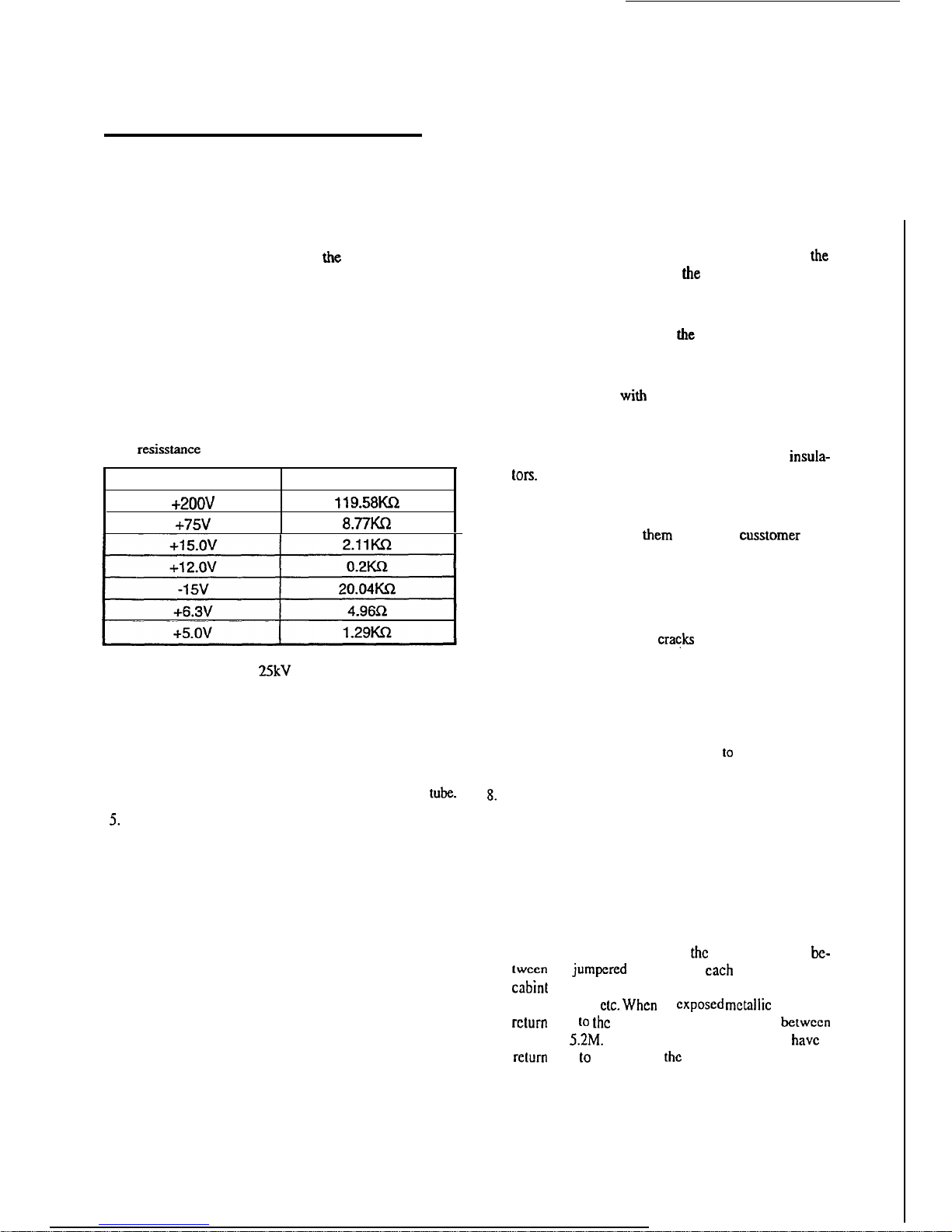
Before turing the display on, measure the resistance
between B+ line and chassis ground. Connect the negative side of an ohmmeter to the B+ lines and the positive
side to chassis ground. Each line should have more
resisstance
than the following specifications:
B+ Line
Minimum Resistance
+2oov
119.5am
+75v
a.77m
4.
Potentials, as high as
25kV
are present when this display
is in operation. Operation of the display without the rear
cover involves the danger of a shock hazard from the
display power supply. Servicing should not be attempted by anyone who is not thoroughly familiar with
the precautions necessary when working on high voltage equipment. Always discharge the anode of the picture tube to the display chassis before handling the tube.
5.
After servicing, be sure to check the items listed in the
Safety Checkout, below before returning the serviced
unit to the customer.
Safety Checkout
The following checks must be made after correcting
the
original service problem and before the unit is returned to the
customer.
1.
2.
3.
4.
5.
6.
7.
8.
Check the area of your repair for unsoldered or poorly
soldered connections. Check the entire board surface for
solder splashes and bridges.
Check the inter board wiring to ensure that no wires are
pinched or coated
with
high-wattage resistors.
Check that all control knobs, shields, covers, ground
straps and mounting hardware have been replaced.
Makde absolutely sure you have replaced all the
insula-
t0l-S.
Look for any unauthorized replacement parts, particu-
larly transistors, that may have been installed dueing a
previous repair. Point
them
out to the
cusstomer
land
recommend their replacement.
Look for parts which, though functioning, show obvious
signs of deterioration. Point them out to the customer
and recommend their replacement.
Check the line cord for
cracks
and abrasion. Recom-
mend the replacement of any such line cord to the
customer.
After making any repair, check the B+ and HV to see
whether they are at the values specified. Make sure your
instruments are accurate; if your HV meter always
shows a low HV, check the meter lo ensure it is not
malfunctioning.
Carry out the leakage current checks as detailed below
overleaf.
Leakage Current Cold Check
1.
Unplug the AC cord and connect a jumper between the
two prongs on the plug.
2. Turn on the display power switch.
3.
Use an ohmmeter to measure
the
resistance value
bc-
twcen
the
jumpered
AC plug and
each
exposed metallic
cabint part on the display, such as screwheads, terminals
control shafts.
etc. When
an
exposed metallic
part has a
return path to the chassis, the reading should be bctwccn
240k and
5.2M.
When exposed metal does not
have
a
return
path lo the chassis,
the
reading must be.

Leakage Current Hot Check How to Find A Good Earth
1.
Plug the AC cord into the AC outlet. Do not use an
isolation transformer for this check.
2. Connect a
1.5k,
10 watt resistor in parallel with a 0.15F
capacitor between each exposed metallic part on the set
and a good earth ground (see How to Find a Good Earth,
below) as shown in the diagram below.
A cold water pipe is a guaranteed earth ground; the cover plate
retaining screw on most AC outlet boxes is also at earth
ground. If the retaining screw is to be used as your earth
ground, verify that it is at ground by measuring the resistance
between it and a cold water pipe with an ohmmeter. The
reading should be zero (0) ohms. If a cold water pipe is not
accessible, connect a 60-100 watt trouble light (not a neon
lamp) between the hot side of an AC power receptacle and the
retaining screw. Try both slots, if necessary, to locate the hot
side of the line. The lamp should light at
normal
brilliance if
the screw is at ground potential
r
.
Leakage Current Hot-Chedc Circuit
AC
VOLTMETER
Example of Leakage Current Hot-Check Circuit
3.
4.
5.
6.
Use an AC voltmeter with 1000 ohms/volt or more
sensitivity to measure the potential across the resistor.
Check each exposed metallic part, and measure the
voltage at each point.
Reverse the polarity of the AC plug in the AC outlet and
repeat the above measurements.
The potential at any point should not exceed 0.75 volt
RMS. A leakage current tester (Simpson Model 229,
RCA WT-540A or equivalent) may be used to make the
hot checks.
Trouble light
Cold water
pipe
How to Check for Earth Ground
Leakage current must not exceed 0.5 milliarnp. If a measurement is outside of the specified limit, there is a possibility of
a shock hazard and the monitor should be repaired and rechecked before it is returned to the customer.
cm
i-
Disassembly Instructions
r
PaH 1.
VA Version
.-
2.1.
Removing the Rear Cover. . . . . . . . . . . . . . . . . . . . .
2-1
2.2.
internal Disassembly (Right Side). . . . . . . . . . . . . . .
2-l
2.3.
Internal Disassembly (Left Side). . . . . . . . . . . . . . .
O
2-l
2.4.
Removing the Neck Board and Main Board . . . . . . .
2-2
2.5.
Removing the Control Board. . . . . . . . . . . . . . . . . . .
2-2
.-
Part 2. Non-VA Version
2.6.
Removing the Rear Cover.
.................... 2-3
2.7.
Internal Disassembly (Right Side).
..............
2-3
2.8.
Internal Disassembly (Left Side).
...............
2-3
2.9.
Removing the Neck Board and Main Board
.......
2-4
2.10.
Removing the Control Board. ..................
2-4
??
VA Version
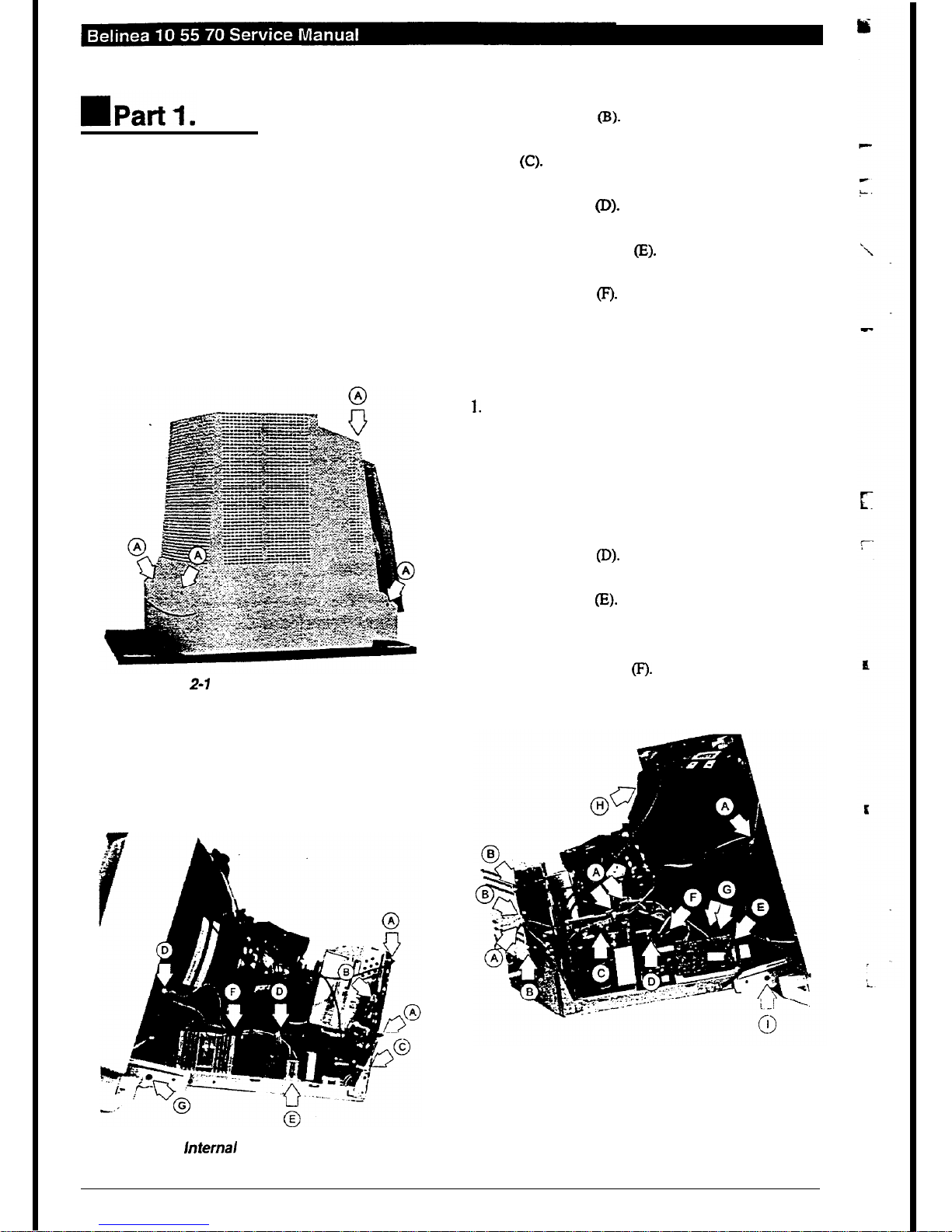
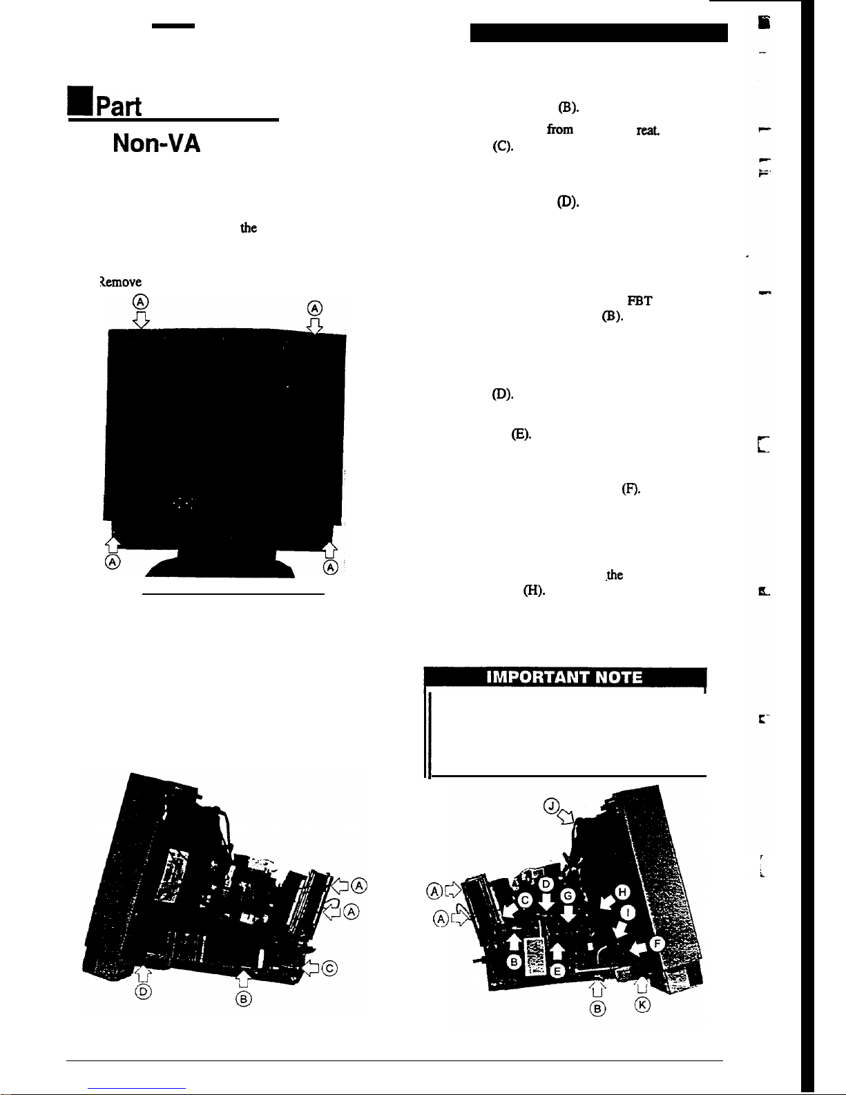
2.1. Removing the Rear Cover
1.
Turn the display so it is resting face downwards on the
work surface. Be sure to place a cloth or other soft
material on the work surface to avoid scratching the
screen surface.
2.
Remove the four screws at the rear of the display. Refer
to the figure 2-l (A).
3.
Remove the rear cover.
Figure
2-1
Remove the Rear Cover
2.2. Internal Disassembly (Right Side)
The neck board is plugged on to the CRT neck and is enclosed
in a metal shielding.
1.
Disconnect the two ground wires from the Neck Shield.
Refer to the figure 2-2 (A).
Figure 2-2
internal
Disassembly (Right Side)
2.
Remove the connected pin from the Neck Board. Refer
to the figure 2-2 (B).
3.
Remove the screw at the rear chassis. Refer to the figure
2-2 (C).
4. Cut the two cable ties indicated to free the cables. Refer
to the figure 2-2 (D).
5.
Disconnect the degaussing coil from the Main Board.
Refer to the figure 2-2
Q.
6.
Release the cable wire indicated to free the cables. Refer
to the figure 2-2
(F).
7.
Remove the nylon revets holding from Bezel. Refer to
the figure 2-2 (G).
2.3. Internal Disassembly (Left Side)
1.
Cut the four cable ties indicated to free the cables. Refer
to the figure 2-3 (A).
2. Disconnect the three ground wires from the Neck
Shield. Refer to the figure 2-3 (B).
3.
Remove the screw at the FBT cover. Refer to the figure
2-3 (C).
4.
Remove the nylon revets holding from fix plate. Refer
to the figure 2-3 (D).
5.
Remove the connected pin from the Logic Board. Refer
to the figure 2-3 (E).
6. Remove Logic Board.
7.
Remove the connected pin from the Connector Board.
Refer to the figure 2-3
(F).
8.
Remove the two connected pins from the Main Board.
Refer to the figure 2-3 (G).
Figure 2-3 Internal Disassembly (Left side)
2-l
cr
E
c
-
To avoid risk of electric shock, before
re-
moving the anode cap, made sure tdhe
a&
ode has been completely discharged as
high voltage may remain on the anode for
extended time after power off.
9.
Remove the anode cap from the CRT. Refer to the figure
2-3
(H).
10. Remove the nylon revets holding from Bezel. Refer to
the figure 2-3 (I).
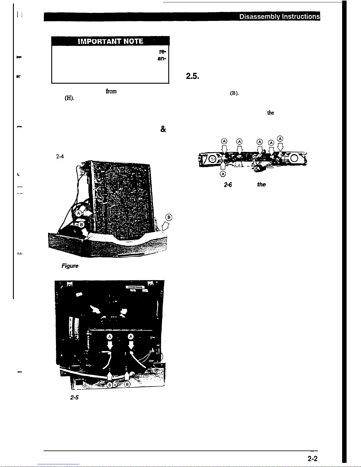
2.4. Removing the Neck Board
&
Main Board
1.
Remove the screw from U Bracket. Refer to the figure
2-4
(A).
figure
2-4 Remove the Control Panel
Figure
Z-5
Remove the Neck Board and Main
Board
2 Remove the two Lock Caps from the
nylon ties.
Refer to
the figure 2-5 (A).
3.
Remove the two ground wires from the Neck Shield.
Refer to the figure 2-5 (B).
4.
Remove the Neck Shield.
5.
Remove Neck Board.
6.
Remove the Main Board.
2.5. Remove the Control Board
1.
Remove the two screws from Control Panel. Refer to
the figure
2-4 (B).
2.
Remove the Control Panel.
3.
Remove the six screws from the Control
Board.
Refer
to the figure 2-6 (A).
4.
Remove the Control Board.
Figure Z-6
Remove
the
Control
Board
-
2-2
UPart
2.
??
con-VA
Version
2.6.
Removing the Rear Cover
1.
Remove the four screws at the rear of the display, and
lift the cover vertically away from the monitor. Refer to
the figure 2-7
(A).
2. 1
Xemove the rear cover.
Figure 2-7 Remove the Rear Cover
2.7. Internal Disassembly
(Right Side)
The neck board is plugged on to the CRT neck and is enclosed
in a metal shielding.
1.
Disconnect the ground wires from the metal casing of
the neck board. Refer to the figure 2-8 (A).
Figure 2-8 Internal Disassembly (Right Side)
2.8.
Internal Disassembly (Left Side)
1.
2.
3.
Disconnect the ground wires from the metal
casing
of’
the neck board. Refer to the figure 2-9 (A).
Remove the two screws from the
PBT
cover and U
bracket. Refer to the figure 2-9 (B).
Rmove the ground pin from the neck board. Refer to the
figure 2-9 (C).
4.
Cut the cable tie indicated to free the cables. Refer to the
figure 2-9
0).
5.
Remove the nylon revets holding from Bezel. Refer to
the figure 2-9 (E).
6.
7.
8.
9.
Disconnect the ribbon cable from the Logic Board and
the cable from the CRT connected to the rear side of the
logic board. Refer to the figure 2-9
(P).
Remove the Logic Board.
Remove the connected pin from the Connector Board.
Refer to the figure 2-9 (G).
Remove the connected pin from
the
Main Board. Refer
to the figure 2-9 (H).
2.
Disconnect the degaussing coil from the main board.
Refer to the figure 2-8 (B).
3.
Removing the screw from the chassis mat. Refer to the
figure 2-8 (C).
4.
Place the display flat on
its
face and remove the nylon
revets holding the main board in place on the frame.
Refer to the figure 2-8 (D).
10. Remove the connected from Main Board, and the connected from Main Board to Earphone Board.. Refer to
the figure 2-9 (I).
To avoid risk
of
electric shock, before re-
moving the anode cap, made sure tdhe an-
1
ode has been completely discharged as
high voltage may remain on the anode for
extended time after power off.
0
A[
@
Figure 2-9 Internal Disassembly (Lift Side)
2-3
1
c
F
I-
-.
-
-
11.
Remove the CRT anode cap. Refer
to the figure 2-9
(J).
12. Place the diiplay flat on its face and remove the nylon
revets
holding the main board in place on the frame.
Refer to the figure 2-9 (K).
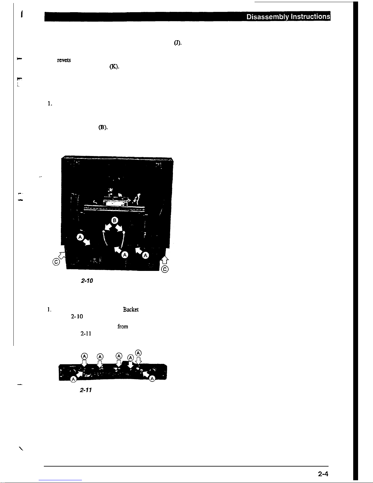
2.9.
Removing the Neck
Board and
Main Board
1. Disconnect the three ground wires from the metal casing
of the neck board. Refer to the figure 2-10 (A).
2.
Remove the two
Lock
Caps from the nylon ties. Refer
to the figure 2-10 (B).
3.
Remove the Neck Board from the CRT.
4.
Remove the Main Board.
Figure
Z-10
Removing the Main Board
2.10. Removing the Control PCB
1.
Remove the
two
screws from Backet Cover. Refer to the
figure 2- 10 (C).
2.
Remove the seven screws from Control Panel. Refer to
the figure 2-11 (A).
3.
Remove
the Control Board.
Figure
2-11
Removing the Control PCB
2-4
Notes
c
1.
2-5
I
-
Part 7. VA Version
3.1.
3.2.
3.3.
3.4.
3.5.
Switching Power Supply
.......................
3-1
The Deflection Circuit ........................
3-3
Video Amplifier
.................I...........
3-11
Microprocessor and Sync Processing.
...........
3-12
Audio Amplifier
.............................
3-12
Part 2. Non-VA Version
3.6.
Sw.itching
Power Supply ......................
3-13
3.7.
The Deflection Circuit ........................
3-15
3.8.
Video Amplifier
.............................
3-23
3.9.
Microprocessor and Sync Processing. ........... 3-24
3.10.
Audio Amplifier
.............................
3-25
??
Part 1.
bA
Version
3.1. Switching Power Supply
The switching power supply (SPS) used in this display is a
15OW flyback mode type. The power supply provides seven
outputs (B+, 75V,
lN,
-15V, 6.3V ,+12V and +5V). Please
refer to schematic diagram for details of the circuit layout. The
input voltage is from
85VAC - UOVAC
with an input
frequency of
47Hz -
63Hz, as shown in Figure 3-
1.
The current first passes through the EMI control circuit and
is regulated to DC by the bridge diodes
(BDl)
and filter
capacitor (C9). During rectification a large current surge is
generated and as C9 has a very low impedance while being
charged the fuse, on/off switch and bridge diode are all liable
to be damaged. For this reason, a thermal resistor (THh4ER)
is added before the bridge diode in order to limit the large
current surge generated during the charging of the capacitor.
During rectification, Cl2 is charged through R7, R12 and
42.
When Cl2 is charged to 16V, IC2 3842A starts to operate (for
details, of the functions of this IC, please refer to the relevant
data sheet) and outputs a pulse signal from Pin 6 to set the
transistor Q6 in the ON state. At this time, transformer T3.
which is connected in parallel, starts to store power. When the
current passing through the resistor R45, and the supplementary current from R39, R41 and R27 (Pin 4 to Pin 3) into Pin
3 of IC2 reaches 1.1 V, IC2 is reset, causing the energy stored
by the transformer to reach the rated value. In order to prevent
the transformer from being saturated and causing damage to
the transistor, when transistor 46 is in the OFF state, the
energy stored in the transformer T3 is released into the secondary coil and is regulated through the various output loops and
filters and converted to the required DC output. In addition to
this, at the appropriate time, the windings pin 1 - pin2 supply
Pin 7 of IC2 with a fixed power supply for normal operation.
Also, when windings pin1
-
pin3 are in power saving active
state, power is supplied to Pin 7 of IC2 for normal operation.
In any of the above cased, the output pulse is terminated and
the FET is turned off, causing the voltage on the output of the
FET to rise rapidly, and the voltage across the winding of the
primary to reverse in polarity, thus tending to reset the flux
within the core. At this point, the diodes D16-D19, D22 and
D24 on the secondary supply winding become forward biased
and begin to conduct, thus transferring energy from primary
to the secondary, and charging the secondary capacitors.
There is also secondary winding the primary side of the power
supply which, through diode D8 and Q5 recharges the control
IC reservoir capacitor C12. This supply then keeps the IC
running. In the event of a secondary short circuit, the supply
fails to recharge, thus the voltage across Cl2 drops to a
threshold limit below which the IC cuts out and returns to its
low current load operation.
During normal operation, the supply rails charge until the
error amplifier realized by IC4 on the secondary begins to turn
on the opto-coupler,
PHl.
At this point, the photo-transistor
of this opto-coupler on the primary side begins to conduct.
draining current from the primary control IC supply through
diode D6. This reverse biased the gate of the thyristor
42.
As
POWER
XFORMER
O/P
RECTIFIER
FILTER CIRCUIT
--,
75v
-›,
15v
-b 12v
+
-15v
-b 6.3V
--b
5v
E
-.
-
-
E
, .
i
FM MONITOR H.V. FEEDBACK
Figure
3-7
Switching Power Supply Block Diagram
3-1
the anode of 42 is fed from an alternating source, once the
gate is reverse biased, this device is then turned off until the
c
current in the opto-coupler drops to zero, thus eliminating the
power that would otherwise be washed in the start-up resis-
tors, R7 and R12.
b
Under normal operation IC4 regulates the current flow
through
PH 1, and hence determines the output voltage of the
error ampliier internal to IC2. Various passive components
around IC4 and IC2 set the gain compensation for optimum
stability and regulation characteristics.
In the event of a fault condition occurring, either Q4 may be
turned on by the lack of voltage at pin2 of IC2 or zener diode
ZDl
may conduct, due to excessive voltage on the primary IC
supply. In the latter case, the triac 43 will fire, thus dragging
down the output of the control IC error amplifier, which in
turn will limit the duty cycle and reduce the output voltage. It
will stay in this mode until the AC input power is removed.
--
When the
feedback
signal passing through the main 75V
output is completed, the transistor’s duty cycle is adjusted
through the transfer to Pin 2 of IC2 3842 of the primary coil
by
PH14N35
and IC4 TL431, stabilizing the output current.
At this time, it is important to note that before the feedback
signal is established, the charge level of Cl5 cannot trigger
43
SCR or it will cause a faulty power startup. In addition, in
order to synchronize the supply power and mdtiitor and reduce
noise that will cause interference to the display, in the area
Dll the monitor’s feedback transformer gets a feedback
signal in order to ensure synchronization between the power
supply and monitor, with synchronization in the range 3OkHz
-
69kHz. Because the power operating frequency changes
with the monitor causing changes in the value of IP, (the value
of LP is fixed while the value of IP increase or decreases
according to the frequency), this affects the test value of Pin
3 of IC2 3842A. This causes the total power supplied to vary
according to the frequency, so a compensation value is provided by D12 in order to reduce the difference in total power
for different frequencies. In addition, because the AC input
ranges from 85VAC to 270VAC, this causes the value of the
direct current on the DC bus to vary, affecting the rise rate of
IP, the oscillator and the duty cycle, and causing the test value
obtained at Pin 3 of IC2 to vary. To resolve this, a compensation value is provided by R39 and R41 which reduces the
difference resulting from the different input voltages.
3.1
.l. Auto-degaussing
.
-
When Pin29 of P2 connector is in high state, the
transistor Ql
2SC945P
is on, causing the relay to
jump from Normal Open (N.O.) to Normal Close (N.
C.) to perform auto-degaussing operations. The duration of this operation is controlled
by
a logic pulse
and lasts approximately 6 (six) seconds. When transistor Ql enters the OFF stale and the relay returns
to N.O. to terminate the auto-degaussing operation is
completed.
3.1.2. Suspend Mode Operation
Two feedback ratios can be selected, both sensing
from the 75V rail. In the event of QX being turned on
by micro processor, additional current is drawn from
the virtual earth node of IC4, thus causing the power
supply to serve the rail to a high voltage, nominally
75V. This is trimmed by resistor
VRl.
The other
supply rail are predetermined ratios of this winging,
being
+15V,-15V&.3V
and
+2OOV
nominally. In
addition, a low voltage primary side winding feeds
the control IC directly through D7 turning off the
control IC supply through Q5, which would otherwise dissipate excessively.
When Q8 is turned off, the 75V rail drop to around
17V.
In this case, the primary control supply fed
through D7 drops to a value that is below the level
needed to sustain operation. Instead, Q5 begins to
conduct and the higher voltage supply winding taken
via D8 is used to keep the primary side powered up
with minimal power losses.
The 5V power supply is driven by one of two sources,
In normal operation when the 75V is present, the
5V
regulator, IC6, is fed from the 15V rail through diode
D21. When switched to standby mode (75V rail
drops to 12V) then the 15V rail drops too low to
supply IC6. In this case QIO and Ql 1 take over and
maintains the supply to IC6 at around 9V.
In addition to the 5V regulated supply, in normal
operation there is also a 12V regulated supply take
from the 12V rail.
To ensure that micro processor gets a good 5V power
supply, there is a power good detection circuit
formed by IC3. This monitors the supply going into
the 5V rail (not the 5V rail directly). It detects
whether there is sufficient voltage to enable the
5V
regulator to work effectively. It
is
not a detection of
the 5V rail itself, but relies upon the premise that the
regulator is not faulty and that there is no faulty load
condition on the 5V.
During power up, there is a delay to the signal at the
output of the threshold comparator IC3 a caused by
R57 and C3 1, in order to allow the micro circuit time
to stabilize. The threshold is chosen such that the
RESET line drops low at least 25ms before the
5V
drop out of regulation.
Finally a synchronization pulse taken from the hori-
zontal output stage maintains the SMPS operating
frequency in sync with the horizontal scan. Dl 1
injects a pulse which prematurely triggers the oscillator within IC2 which would
othcrwisc
run at a
frequency lower than the minimum
required
sync
frequency.
DC to DC Circuit
Another special characteristic of this power supply is
the addition of a DC to DC circuit to the output. In
order to support the monitor at different frequencies,
a similar high voltage is required (26kV). To accommodate this requirement, a buck loop has been added
to the 200V output. The synchronization signal is got
3-2
from the monitor H.D. area, and after getting syn-
chronization through
QPl
trigger pin2 of
ICP2,
a
high voltage feedback signal ( FB). is input to QP2
to obtain the DC level. A comparison is carried out
between pin5 of ICP2 and ICP3 to establish the duty
cycle of transistor QP3 so that even under different
frequencies, a similar high voltage value is still obtained.
3.2. The Deflection Circuit
9.
10.
11.
Please refer to the block diagram of the deflection circuit and
video circuit and logic circuit as shown in Figure 3-2.
36.1. IC308
UPC1883
12.
13.
1.
2.
3.
4.
5.
6.
7.
8.
IC308
UPC1883 is a horizontal and vertical
processor. The horizontal section consists of a
‘ITL interface, two comparators and an oscilla-
tor. The vertical section consists of a
TlL
input
interface and an oscillator. This IC includes a
voltage stabilizer to provide about 5V.
When sync is input as a
TIL
level, this causes
a negative edge trigger. Pin 26 serves as the
H-sync input point and Pin 27 as the V-sync
input point.
14.
15.
16.
Pin 18 is the horizontal output. The output
current is too small to drive
T301,
therefore
4374 and 4375 are added as a buffer followed
by a transistor 43 10.
17.
Pin 20 and 22 provide the external control of
the horizontal oscillator free run. Free run is
controlled by changing the resistance value of
R479 and C431 to obtain different DC voltage
levels. By adding an external F/V on Pin 19, the
difference between a variety of input frequencies and free run is maintained at a similar lenel.
In this way, when different timing modes are
input, if the ration between the active display
and total display is similar, then the position of
the phase will also be similar.
3.2.2. Vertical Deflection Circuit
1.
X202
TDA8172 consists of a flyback gener-
ator, voltage stabilizer, drive circuit and verti-
cal output amplifier.
2.
The vertical oscillator circuit
(a) The frequency and phase of
rhe
vertical
oscillator circuit is generated by the vertical
synchronization signal.
The parallelogram of different modes can be
individually adjusted by changing the VDC
level at pin 4.
The pin-balance of different modes can be in-
dividually adjusted by changing the VDC level
at pin 5.
The vertical size of different mode can be indi-
vidually adjusted by changing the VDC level
at pin8.
The vertical center of different modes can be
individually adjusted by changing the VDC
level at pin 11.
The vertical linerarity of different modes can
be individually adjusted by changing the VDC
level at pin 12 and 13.
The horizontal phase of different modes can be
individually adjusted by changing the VDC
level at pin 25.
The horizontal duty of different modes can be
individually adjusted by changing the VDC
level at pin 23.
When it is not use for pin 1 to pin 5, it shall be
connected to Vcc (9V).
The pin 2 and pin 4 are setting the trapezoid or
parallelogram and output waveforms from the
pin 28. pin 3 and pin 5 are setting the side pin
or side pin balance and output waveforms from
the pin 10.
Pins 6 provides the external control of the vertical oscillator free run. Free run is controlled
by changing the
capcitance
value of C432 to
obtain different DC voltage levels. It does not
need an external F/V control because this IC
can keep vertical synchronization. Pin7 pro-
vides vertical A.G.C function.
The pin-comer of different modes can be indi-
vidually adjusted by changing the VDC
level
at pinl.
The trapezoid of different modes can be indi-
vidually adjusted by changing
the
VDC
level
at pin2.
The pincushion of different modes can be indi-
vidually adjusted by changing the VDC level
at pin3.
(b) The synchronization signal is input from
Pin 27 of
LC308
UPC1883, after being proc-
essed by the synchronization circuit, is sent to
the vertical synchronization oscillator circuit to
trigger the vertical oscillator and synchronize
the oscillator frequency with Ihe external synchronization signal. The frequency of its internal free
osciilalion
is set by the time constant
of C432. It
dots
not
need
an cxrernal
F/V
control
because
this
IC308
can
keep vertical
synchronization. Pin 7 provides vertical A.G.C
function, so the pin 7 of IC308 is use to maintain the difference between the free oscillation
frequency and external synchonization signal
frequency at a similar level and make the sawtooth wave amplitude from pin 9 of IC308 the
same.
t
-.
L
1
: ’
L.
3-3
I
I
,
t’
-
I
1
PAWCS)
AMPI
IFICR
I
1
I
-
???
?
????
??????????
?
???????
CtRCUIT
lC503
IYcu-TI@
b
SYNC ON GREEN
ClRCUlT
IC504
v
moo
I
.
.
OSD CiRCUlT
IC502,Q511 ,Q512,Q513
L_,
1
I
t
RGA’N
:
7
DAC CIRCUIT
-
I I
G
GAIN
0PM-
@GM
.
IC505TDA8444
SBuIcowRol
c
Gl
I
(
-18OV)
I
I I
WV
BLANKING
1
1
HRET
--------iv
.
WET
I
CIRCUIT
Q503,Q505,Q509
.
A
X-RAY CONTROL
I I
.
4
I
]
CIRCUIT
Q370.Q371
.
L
I
I
I
II t
‘H
SdC
1
HSYNC+
7
c>-
COMBINE0
HORKONTAL
6
MRTICAL
PRoCESSof?
WrTH
GEOMETRY
CONTRol-”
DYNAMIC
Pocus
CIRCUIT
T401,CMlO
4420
+-
H-WIOTH
CONTROL
CS CONTROL
CtRCUlT
E>-
CIRCUIT
IC302,4360
.
-t>-
4350,4302,Q309
Q353.Q354,Q355
RL301
,Q347,0348
I
B*
CONTROL CIRCUIT
4
QPl
,QPZ,QP3,QP4,
R-SIDE
ic,
CNO
!o,/-
AUDIO PREAMPLIFIER
CIRCUIT
ICQOl
L
?
L-SIDE
3;
1
lJPc1408HA
A
W
b
3.
Vertical Si Control
The pulse voltage output by the oscillator is
sent to the sawtooth wave generator. The size
and amplitude of the voltage of the sawtooth
wave generation can bc changed by DC value
which output from Pin
IO,1
1 of IC306 and the
vertical size can thus be controlled. This sawtooth wave voltage passes through a buffer and
is output from Pin 9 of IC308 to pin 1 of IC202
TDA8172 of the vertical drive circuit.
The verticai ramp and DC offset are also controlled by DAC output. The vertical ramp generated across C432 is buffered internally to
IC308
by DC controlled variable gain stage.
The voltage is derived by sum of 2 DAC output,
VSIZEl
and
VSIZE2.
which are summed to-
gether to give 128 bit resolution.
4. Vertical Drive Circuit
(a) It is not sufficient to rely solely on the
oscillator circuit output to ensure the stability
of the vertical output, so a first or second level
amplifier circuit must be inserted between the
oscillator circuit and the output. This circuit is
called the drive amplifier and in
-addition
to
amplifying the sawtooth wave also corrects the
vertical linearity.
After adding the drive circuit, because the level
of amplification can be considerable, enough
negative feedback can be added to correct vertical linearity and increase the stability of the
circuit.
(b) If the current of the sawtooth wave flowing
through the deflection yoke is distorted, then
the top and bottom portions of the display will
be expanded or compressed, resulting in poor
linearity. In order to solve this problem, correction of the linearity of the sawtooth wave can
be carried out before the drive level.
5.
IC202 TDA8172
Vertical Drive Circuit
The IC202 uses a double power source, so it
can be viewed as an OCL drive ampiification
circuit.
In order
that
the DC coupled output stage accurate DC reference, a DC reference voltage is
taken from IC308 from
pin 12.
This used as the
reference voltage (via divider resisdtors, R497
and R499) for the DC coupled power amplifier,
IC202. This is 8 simple voltage to current in-
verting amplifier, using R203 to derive a voltage proportional to the current in the dcflcction
winding of the yoke. This voltage is fed back
to the virtual signal earth inverting input of the
power amplifier(pin1) by R204. This back to
back diode feedback network modifies the
linearity of the transfer characteristic in order
to give precept “S” correction linearity. in ad-
dition to the variable correction in the ramp
generator.
The vertical output amplifier has a voltage
boost circuit to triple the positive supply volt-
age during retrace in order to speed up flyback.
It does this by charging capacitor C202 through
diode D212 during the normal forward scan.
Pin6 of the IC is the voltage supply to the power
output stage. When
flyback
occurs, pin3 is
switched to the positive supply rail on
pi&
thus adding the voltage across C202 to that of
the supply rail, effective doubling the supply
momentarily.
6.
Vertical Centering Adjustment
Since IC202 functions as an OCL circuit, VDC
is output from Pin 7 of IC202, so the central
current can be changed to shift the on-screen
display up or down to prevent voltage
fluctua-
tion. After adjusting the power stabilizer at Pin
14 of IC308 UPC1883 (about 5V) and pin 11
of
IC308
with R487, R497 and R499 this is
input to Pin 7 of IC202 to change the value of
the vertical center.
The DC operating point of the amplifier can be
varied by the VPOS DAC output which adds
or subtracts an offset into the output, thus varying the DC offset of the scan and hence the
vertical centring.
3.2.3. Pincushion Correction Circuit
1.
If the width of the border in the center of the
screen is insufficient, the waveform
shown
in
Figure 3-3 below,
can
be used to add to hori-
zontal deflection B+ in order to change the
deflection of the horizontal deflection circuit.
%
This waveform is the parabola obtained after
regulation of the vertical period, and is created to
perform amplitude modulation on the horizontal
deflection current, as shown in Figure 3-4.
/-J&J&
Figure 3-3
Vdtage
Correction Wave
-
FH: Horizontal Frequency
FW Vertical Frequency
Figure 3-4 Current Correction Wave
3-5
--
e
I.
tor output, is added to horizontal B+
to provide
pincushion distortion correction.
‘Ihe
diode modulator pm-amplifier provides
this filtering action. The op amp IC302 is con-
figured with 4353
to
provide a current source
output at the collector of 4353 . The
PWM
parabola is filtered to remove horizontal rate
harmonics by 657.
r
3.2.4. Structure of Horizontal Deflection Circuit
The function of the horizontal deflection circuit is to
cause left/right scanning of the electron beam using
the sawtooth wave current flowing through the horizontal deflection yoke, and is made up of the horizontal oscillator circuit, horizontal drive circuit,
horizontal output circuit. synchronous AFC circuit
and high voltage generator circuit.
!--
1.
Horizontal Drive Amplifier
In order to rapidly saturate the output transistor
(ON) or cut it off (OFF), a sufficient basic
current must be provided. Because of this, an
amplifier circuit is added between the oscillator
circuit and the output circuit to amplify the
pulse voltage. At the same time, after the waveform has been regulated, by adding this circuit
to the
output circuit, this amplification circuit
functions as a drive amplifier.
:
I-
2.
The
sawtooth wave is Atput from Pin
.lO
of
IC308 and
through C354 and R360 and input
to Pin 2 of IC302. It
is then output from Pin 1
of IC302 and after being sent to Q353’s collec-
2.
IC UPC1883 consists of a vertical sawtooth
wave generator, horizontal sawtooth wave generator, horizontal oscillator circuit, vertical oscillator circuit, AFC circuit, phase regulator
circuit, geometry control circuit and drive am-
plification circuit. This IC includes the vertical
and horizontal circuits combined in one package.
When the synchronization signal input to Logic
circuit and pin 26 of
IC308.
The pin 18 of
IC308 output horizontal frequency is achieved
by the pin 12 and pin 13 of
IC306
(D.A.C
control) and flyback
pulse
from
pin 6 of T302
(A.F.C) fed to pin 17 of IC308, so the pin 18 of
IC308
output horizontal frequency through
4374,
4375.
Q3 10 and
I301
provide a hori-
zontal output transistor base current of
430
1.
The horizontal output transistor base drive
is
taken from a conventional base
drive
trans-
former stage. This circuit
as in a similar manner
to a flyback power supply. The square wave
horizontal oscillator output signal is coupled
into the base of base drive stage transistor,
Q310,
via C334,
C330,
D333, R326,
R325,
Q3 10 turns on and connects the primary winding of transformer ‘I301 across the +15V and
-
15V supplies. This causes the primary current
to increase linearly until such time as 4310
turns off, hence storing a predetermined
amount of flux energy in the transformer. As
43
10 tums off, and the primary current falls to
zero, the secondary voltage is driven above the
threshold of the base-emitter junction voltage
of the horizontal output transistor, 4301. Current flows through
R304,
R457, R329 and
D3 12 into the base of 4301 hence turning this
device on. The high base current of around
1.lA.
Lamps is so high
that
4301 is driven
heavily into saturation. This is important in
order that the collector voltage should be as low
as low as possible whilst conducting the high
peak currents that flow through the horizontal
deflection winding. In turn.
this is vital to limit
dissipation.
At the required time as determined by the hori-
zontal oscillator, the base drive transistor is
turned back on. The voltage at 4310 collector
fall rapidly back towards the -15V rail. However, the secondary current still remains flowing in a positive direction for a short time, due
to the finite leakage inductance of T301. Also,
due to the heavy saturation of Q301, the base
voltage remains at around IV. The current in
the secondary winding rapidly reverses and
goes sharply negative as the charge stored
within the base region of
4301
is removed
Diode D312 helps to speed up this charge re-
moval. Note that during this time, the collector
output of the
4301
is still turned on, even
though the base current is flowing out of the
base.
This period of time is known as the storage time
of the device and may take between
2-3~s
depending upon peak collector current and
temperature and various other design factors.
Finally, when all charge in the base region of
4301
is dissipated the base current suddenly
stops, and the secondary current drops almost
instantly to
zero. At
that point, the device now
become non conducting and the collector current flow also terminates. The secondary voltage on T30 I drops to it’s unloaded voltage and
the current flow in the primary settles to it
initial value once more.
3.
Horizontal Output Circuit
The horizontal output circuit uses the switch
operation of a transistor and a damping diode,
and provides a sawtooth wave current to the
dcllection
yoke.
The horizontal deflection yoke
is made up of
the
L
value
on
the
coil and
resistance r inside the coil connected in series.
Its resistance is extremely small, and the time
constant
(Vr)
is extremely
large.
Because of
this
the voltage at
the
two
terminals
of
the coil
cause rapid variation in the current flowing in
the coil still will slowly vary, creating a saw-
3-6
tooth current.
‘l%e
basic circuit and equivalent
circuit are shown in Figures 3-5 and 3-6.
Damping diode
figure
3-5 The Basic Deflection Circuit
Figure 3-5 Equivalent Circuit
4.
Horizontal Output Equivalent Circuit
Operation
Refer to Figure 3-7 above for the current wave
of the voltage of the horizontal output circuit
during operation.
(a)
tl-
t2
Period
The base of the output transistor is added to the
forward bias voltage. As the current through
the base is very large, it will cause the output
transistor to be saturated, corresponding to the
ON state of S 1 in the equivalent circuit. At this
time the deflection yoke contains a current flow
and because the time constant is large. the
current will slowly show a linear increase as
shown in Figures 3-7 (b) and 3-8 (a).
(b) t2-t3 Period
At
t2.
a negative load is applied to the to the
base and the output transistor changes to OFF
(Sl
in open state). There is no current passing
through the transistor at this time and the L and
C components of the deflection yoke become
independent oscillation circuits. If the current
is suddenly cut off, then the polarity of the
inverse voltage generated at L will be as shown
in Figure 3-8 (b). This voltage is viewed as the
source voltage and will cause current to flow,
at which time the current flowing to C is as
shown in Figure 3-7 (d). At time 13 this current
is 0 but the voltage at the two capacitor terminals is at maximum. This waveform is known
as flyback pulse, and is
shown in Figure 3-7
(0.
(c) (U - t4) Period
The energy accumulated in C is released to the
deflection yoke, the direction of the current
flow being shown in Figure
3-8 (c). The current
increases as the voltage
onC
decreases, and at
time t4, the voltage of C is 0, at which time the
current is at maximum, which means the cur-
rent flowing into the deflection yoke is also
maximum.
C is then charged and if a damping
resistor is not
co~ected, the
energy between L
and C will be reversed, which is the oscillation
frequency set by the oscillator at L and C.
(d) t4 - t5 Period
At
t4,
the voltage of C is 0. After this it is
recharged in the opposite direction and this
voltage exceeds the voltage of the power source
at time 14. At this time the damping diode is ON
and the L and C circuits are shorted out and stop
oscillating. Because of this the time constant of
r and L in the damping diode is large so the
current flowing
in
the deflection yoke does not
suddenly become 0. The current shows a linear
decrease, and when it becomes 0 at time
t.5
the
transistor is ON and the operation described
above is repeated.
As described above, the current flowing in the
deflection yoke during scanning is the sum of
the current which has passed through the transistor and the damping diode current. Please
refer to Figure 3-7 (e).
(e) Horizontal output operation:
The actual output stage differs from the simple
model described in a number of ways. Refer to
the basic schematic of the major components in
Figure 3-9 on the following page.
The main inductance L is now divided into the
primary winding of the Flyback Transformer
(FBT), T302 and the deflection yoke winding.
The deflecting yoke is coupled through a ca-
pacitor C3
11,
which has two function. Primarily it prevents DC unwanted DC currents
flowing through the deflection yoke which
would otherwise cause an undesirable deflection of the CRT beam.
Secondly, the voltage drop across it due to the
AC ramp current flowing causes a parabolic
modulation in the slope of the ramp, leading to
a progressive curve in the ramp, symmetrical
about the zero current value as shown in Figure
3-10, below. This intentional distortion of the
linear
ramp is required to compensate for the
‘S’.
or symmetric
linearity
distortion in the
CRT.
In series with C3 1 I and the deflection yoke is
another indicter, L303. This is a saturating in-
dictor that is biased with a permanent magnet.
Consequently this device has a linearity that is
higher for current flow in one direction than in
the opposite direction. This function provides
compensation for resistive losses that would
otherwise cause an undesirable exponential
3-7
Transistor ON
/
(a) Base Input voltage
(b) Current through transistor
(c) Current through diode
(d) Capacitor current
(e) Current through deflection yoke
(9
Voltage generated in deflection yoke
Figure
3-7 Horizontal Output Voltage/Current Waves
curve to the linear ramp, resulting in
asymmet-
rical
linearity errors in the displayed image.
In addition to the AC coupling of the deflection
yoke, another major difference is that the
damper diode is split into two diodes. A second
resonant circuit comprising of
C307
and
L304
are connected at this point. This second resonant circuit acts exactly as a smaller version of
the
flyback
circuit. A ramp current is set up in
L304,
proportional to the voltage at the output
of the diode modulator circuit, VDM. A small
flyback
voltage is also created across
C307
as
a result of this. Consequently, the voltage seen
across the yoke winding is the difference
bc-
tween the constant heigh main
flyback pulse
seen across
Q301
and
the
smaller, variable
flyback
pulse seen across
C307.
As the current
flowing in the yoke is proportion to this difference, the deflection current (and therefore the
VDM. This voltage is derived from the output
of 4353 after buffering by a unity voltage gain
amplifier formed by 4354 and 4355.
The voltage seen in the output stage require
special attention. The B+ supply can varying
between
60-
180. The main
flyback
pulse seen
across
4301
and associated components is
around 1200V. Consequently, appropriate precautionary measures must be taken when servicing the monitor.
In addition to the basic topology as
dcscribcd
above, there
arc a
number
of
other
additional
dcviccs.
4302
and 4309 can bc
indepcndcntly
turned
on or off
under
logic control.
These
devices
switch addition capacitors, C3 I3 and
C324 in parallel with C3 I I to alter the amount
of ‘S’ correction at different horizontal scan
frequencies.
displayed image width) can hence bc
modu- D308 and D309 set up a positive and a negative
lated
by varying the diode modulator voltage, supply rail with respect to the main B+ supply.
3-8
(a) Second half of scanning period (tl -
C?)
*
I~+-
(b) First half of return line period
(t2 -
t3)
+
-t/
+T
A
=J
1
I/ P
I
- xi
(c) Second half of return line period (t3 - t4),
(d) First half of scanning period (t4 - t5)
Figure 3-8 Polarity of Transformer Voltage
current into
L303. ‘Ihis
current flows into the
deflection yoke and adds a variable DC offset
to allow image raster entering to be achieved.
The B+ supply is configured so as to maintain
a constant anode voltage. The anode voltage
is
derived from the
flyback
transformer,
T302.
As
the
flyback
voltage across the primary is
al-
ready a high voltage pulse of around
1.2kV,
it
requires only a modest turns ratio to step this
pulse up to around
26kV.
the working voltage
of the CRT.
Figure 3-9 Basic Horizontal Output Circuit
Parabolic voltage
acrOSS
(2311
s’txmeckd
ov
_ - Lineard
amp
--
The
flyback
pulse at the primary of
T302
is
proportional to the
both
frequency and the sup-
ply rail, B+. In order to maintain the anode
voltage at a constant 26kV a regulation system
is required. This is achieved
using a buck regu-
lation stage formed by a
ICP2
driving a
FET,
synchronized by the horizontal oscillator. The
ICP2
has an error amplifier that generates an
error signal from the feedback network formed
by the high voltage bleed resistor (it is internal
to
T302).
Resistors
VRPl,
RP14 and RP13 set
the DC feedback ratio, and by adjustment of
VRP I, this ratio can be adjusted at
setup
to set
the high
voltage
at it’s nominal
value
of 26kV.
The
AC
frcqucncy rcsponsc
of
the scrvc
loop
is set by CPI 1 and RP21 for optimum stability
and relegation
characteristics.
Figure 3-10 Linear Ramp Distortion
Q352 acts as a constant current source that can
be programmed under logic control. This cur-
rent source drives the transistor pair
Q304
and
4305
which thus drive an adjustable constant
The output of
the
error
amplifier
which can bc
observed on ICP2 of pin 5 is
internally
compared with a DC voltage. This DC is produced
across.
CP4, charge by
RW.
The voltage across this
capacitor is periodically discharged by
QPl
which is fed by a pulse from the horizontal
3-9
c
.-
-
drice via RP4 and CP3. This pulse is triger ICP2
and getting the synchtunixation.
In the event of the horizontal oscillator stop
ping, as occurs during mode change etc., the
ramp generator stops functioning, this prevents
operation of the horizontal output stage immediately after the oscillator has stopped in order
to protect 4301 from excessive voltage.
The ICP2 compares the ramp in pin 2 with the
error voltage on pin 5 and produces a pulse
width modulated output on pin 3. This output
drives through a small pulse transformer, TPI ,
to the gate of the FET, QP3. This device acts as
the power switch to the buck regulation stage,
the inductor
LPI
acting as the storage element.
During mode change, the B+ supply can be
instantly turned off by pulling up the error
amplifier input on pin 5 and pin 4. These can
be achieved by QP6, QP4 and QPS which is
driven from the logic signal
PMGTl.
Whilst
QP6, QP4 and QP5 can switch off the B+
supply almost instantly, the time taken for the
supply to restart is programmed by the value of
CP16. This capacitor slowly discharges when
QP6 is turned off, thus allowing the B+ voltage
to follow an exponential rising charge curve,
set by the
value
of CP16 and RP24.
The average beam current through the CRT
also flows
through
the secondary high voltage
winding of T302 connected to pin 8 of T302,
C319 smooths the pulse of current flowing in
the secondary winding and the average DC
current is supplies through resistor R311 and
VR301.
Pin 8 is clamped between 5V and
ground by
D310.
When no anode current is
flowing, the voltage at pin 8 is at the clamp
voltage of 5.5V. When the average secondary
current flowing exceed
46OmA.
this voltage
begins to drop below
this
threshold. Thus a
signal is generated which can be fed to video
amplifier for automatic beamcurrent limiting
(ABL). This is fed into the error amplifier.
APWN signal is used to drive a switching FET
QP3 which drop the voltage down to maintain
a constant EHT, the DC operating point of
which is adjusted by
VRPl.
The horizontal output stage is a conventional
diode modulator type.
3.2.5. Horizontal Size Control Circuit
The different DC value output from Pin
9-10
of
IC307
passes
through
the
distributed voltage from
R359 and R358 achieves one fixed DC value which
is sent to Pin 3 of IC302. so the VDC from Pin 9-10
of IC307 is not the same, causing Pin 1 of IC302 to
output a different
dc
value, after passing though the
buffer, collector of Q353, output to Q354 and Q355
Darlington current amplification though L304 to ad-
just the current though H-DY’s current
value
achiev-
ing size control.
In addition, width control is achieved by adding a DC
offset to the output current at
4353
collector proportional to the DAC outputs on pin 9 and 10 of IC307.
This DC voltage is switched for a constant period by
4360
which is driven by the flyback pulse derived
from pin 6 of the
PBT.
The resultant output is a
current pulse of constant width, which is then averaged by the capacitor
C355.
In this way a voltage
proportional to frequency is gained as the reference
for the non inverting input of
the
diode modulator
pre-amplifier. This in turn will ensure that the width
of the scan produced on the screen is constant for all
frequencies of operation for any given DAC output
The output of the pre-amplifier is a current source at
the collector of 4353. This current is transformed to
a voltage by resistor R365, which is connected to the
B+ supply. In this way, any ripple present on the B+
supply rail as a result of anode voltage loading will
be also seen at the collector of Q353. Thus anode
voltage loading effects, which cause ripple on the B+
line, do not influence the scan width as the width is
proportional to the voltage across R365 i.e. independent of B+ ripple. This voltage is buffered by the
quasi-darlington pair
4354
and
4355
to drive the
diode modulation output stage. To improve effective
screen width regulation, additional compensation for
high voltage ripple is injected into the amplifier by
the network R312, C323 and
C360.
This signal
modulates the horizontal scan amplitude to compensate for loading effects on the anode voltage.
X-RAY Protection Circuit
The feedback pulse voltage from T302 F.B.T
is regulated through D373 to obtain a DC voltage and the appropriate set voltage is distributed by R470 and R47 1. When the feedback
pulse voltage exceeds the set voltage, a DC
voltage develops in the cathode of ZD310
which turns on Q370 and Q37 1. As a result,
48
is turned off (PGMTO is low), putting the
power supply is “OFF” mode. This is the phenomenon of high voltage pretection.
Horizontal linearity and CS Switching
Switching CS is necessary to ensure the lines arc
in
accordance with the specifications in multi-sync
monitors.
Cl
For frequencies
55-68kHz
up, RL301 is ON
and
4302
is OFF
and CS
is C3 1
I.
El
For frequencies
55-42kHz.
RL30 1 is ON and
Q302isONandCSisC313andC311.
0
For frequencies
42-36kHz.
RL301 is OFF and
Q302 is OFF and CS is C3 11 and C324 i n par-
allcl.
3-10
0
For frequencies
36-29kHx,
RL301 is OFF and
4302
is ON and CS is C31
l,C313
and C324 in
1
Mode 1
Hsync Vsync1 PGTMl
1
PGTMOI
I
I
55-68KhZ 42-55KhZ 36-42KhZ 29-36KhZ
I I
I
I
iSCAP
H 1 L
i
H 1 L
1
I
I I
I I
ISCAP21‘
H
I
H
L
L
I
3.3. Video Amplifier
The RGB video and sync signals are supplied through a video
cable directly to the Video Board at connector P501. The RGB
signals are terminated in 75 ohms by R501 and R503, R505
and R506.
The RGB signals then enter an LM1207 video pre-amplifier
IC, providing synchronous black level clamping. variable
picture contrast (gain) and RGB gain balance for color alignment. Separate gain control voltages for the three pre-ampli-
fier
channels are provided via R556, R557 and
R558
from
the TDA8444 DAC which is loaded by the microcontroller
via the 12C bus. These inputs enable the individual gains of
each channel to be varied to allow channel gain balance. In
addition, a common signal is applied on pin12 to adjust all
three channels by the same amount, to allow for overall gain
or contrast control.
A synchronous clamping signal is derived from the horizontal
sync pulse by one half of IC504. This takes the trailing edge
of the horizontal sync pulse, differentiates it through C531,
then squares it via the monostable feedback action of C525
and R513 to provide a precise length digital clamping pulse
which is applied
IC503
via pin14. The timing is shown in
Figure 3-
11,
below.
Video Signal
Clamp Signal
Pin 14 of
ICB
Video signal after
horizontal blanking
NOTE:
A.
Clamp1
signal is
gmemted
from tlyback
time
6. wllen Ihe
Clamp1 signal is less than
1.4vpp. the IC’S inlemal clamp
loop
will
opera1e; wtmn greater
than
1.4vpp.
it
will
not operate.
Figure
3-l 1
Timing of Pin 74 Clamp Signal
The outputs of the video preamplifier are fed to
IC501,
a
hybrid power amplifier IC type LM2419, through resistors
R524, R526 and R528. In addition, on screen display video
information
generated
by IC502 can be injected via diodes
D513.0514
and D515.
IC.501
amplifies the video signals to around
35Vpp.
The
outputs are AC coupled to the CRT cathodes via C523, C5 12
and C513. In order to bias the DC level of the cathodes
correctly, the AC coupled signal is DC restored by clamping
to a DC voltage
which
can be varied under microprocessor
control. Considering Red channel output on
IC501
as an
example, the signal is clamped by D5 17 to the voltage set by
the transistor amplifiers formed by Q502, which amplify the
adjustable voltage at the output of the DAC. A
similar
stage
can be seen for the green and blue channel outputs.
When the
RC~
video signal amplification circuit is added for
amplification, this waveform will change as shown in Figure
3- 12 (a). Without the DC component, as shown in Figure 3- 12
(b),
the DC level of darker and brighter displays will be
different, so when this kind of signal without a DC component
is sent to the CRT, it will cause the contrast of the image to
change as the signal changes. Therefore,
4502
and D5 17
serve as a DC clamp and the CRT’s anode DC voltage can be
adjusted by the DAC.
!y+~&.~~~~L+-
(Dark image) (Bright image)
Average
Layer
Waveform without ti component
Figure
3-72
The Post Output Amplifier Circuit
IC502
is an On Screen Dispay processor. This is a simple
video generation IC that has its own crystal oscillator, X501
by using an internal PhaseLocked Loop (PLL) the IC
can sync
to the incoming vertical and horizontal oscillator frcqucncies
and produce the OSD video signals
once initialized
and
loaded by the commands and data rcccivcd on the
l2C
bus.
When the OSD display is activated, the blanking output of
the
IC502
also sends a signal to the blanking input of
lC503
(pin 13) to provide
an optional black background for the
OSD
display.
The RGB signals arc amplified to
drive
the
CRT by an
LM2419 hybrid amplifier and capacitively coupled to the
cathodes.
Brightness control is achieved by varying the bias of
Gl
of
the CRT
via a transistor stage formed by Q507 which is also
driven by an output of the TDA8444. Horizontal and vertical
3-l 1
blanking signals are coupled into this amplifier to prevent
visible retrace lines.
3.4. Microprocessor And Sync
Processing
The microprocessor
is an
87C54
type. It has 16k internal
masked ROM which contains a basic communication ‘boot’
routine and various other simple routines. It
is also used
to
store the OSD icon bit map. ‘Ibe main firmware routines and
variable data are stored in the 16k external EEROM, IC702.
When the micro is instructed via the RS232 bus, the internal
ROM boot routine will load up the EEROM with program
data from the RS232 bus. Thus it can be made to load its own
firmware. From then on it will run jointly out of EEROM and
internal ROM. Another important routine within the internal
ROM is the routine which allows data writes to be made to
the EEROM. This must be resident in the micro as it cannot
run from the EEROM whilst writing data. These control the
addressing and I/O port selection from the micro,
X701.
AlsospecialixedportsPinl8andPinl9ofIC7O1
formtheIIC
bus
interface which is used internally to set the DAC valuse
and the OSD IC and the
da&
The micro also drives the sync selection circuits. IC704 is
used to set the polarity of the incoming sync signals. IC705
allows the micro to sample the vertical and horizontal syncs
and to select the correct polarity on the outputs HSYNC and
VSYNC appropriately. In addition, whilst sampling the polarity, the micro can measure the frequency of both syncs. By
suitable selection of
HSYNC
and VSYNC control lines,
IC705
can also select the signals derived on HDR and
VRET.These two signals come from the horizontal and verti-
cal oscillators. By measuring these with the internal timers&e
micro can set up the oscillators for optimum lock to the sync
signals. It does this when ever a mode change occurs.
A mode change is detected by either a change in vertical
frequency, which is monitored by firmware, or by a sudden
change in horizontal frequency. IC701 is clocked and reset by
the horizontal sync pulse and the HDR line. If any sync pulse
is not matched by a HDR pulse then an interrupt is created on
the MODEC line.
When power is disturbed to the unit, the power reset line goes
low. This also causes an input to the micro via the MODEC
line. On detecting this interrupt, the micro first checks inputs
PinlOand
Pin15 ofIC701. If these
arealso
low, then it knows
the MODEC interrupt was caused by an impending power
failure. In this case the micro saves the current RAM data in
EEROM and prepares for power off. The RESET line is
delayed for 7ms by R722 and C702 to allow time for the data
to be saved. The REST line then holds off the micro and the
EEROM until power is good once more.
If the front panel ON/OFF button is pressed, a MODEC
interrupt is also created. This time only P3.3 is pulled low so
the micro can detect that the interrupt was from the front
panel. In this case the micro saves the data but flips the bit
which stores the last power on state. The micro is then reset.
When the reset disappears the micro bring up the power in the
opposite state to before, i.e., if the power was off before then
power is now on. In this way the front user on/off switch can
toggle the on/off state and also always act as a micro reset
switch.
3.4.1. DAC Assignments
The DAC assignments are shown in the table below.
3.5. Audio Amplifier
The R/L audio signals are supplied through a P905 directly to
the Main Board at connector
P904
and
P903.
The audio
signals are impedances by R901, R902, R903 and R904. The
R/L audio signals then enter an
UPC1406HA
audio pre-am-
plilier
IC701, providing variable sound control gain. Scparatc
gain control voltage for the two prc-amplifier channels arc
provided by R912 from the IC307 TDA8444 DAC which is
loaded by microcontroller via the
12C
bus. The outputs of the
audio pre-amplifier arc fed to IC702, a hybrid power amplilicr
IC type UPC13 16C through resistors R905, R907 and capaci-
tor C907, C9
11, X702
amplifier the audio signal to around
1.5W maximun. The outputs arc AC coupled to the speaker
via C920 and C924.
apart
2.
??
Non-VA Version
3.6. Switching Power Supply
The switching power supply (SPS) used in this display is a
15OW flyback mode type. The power supply provides seven
outputs
@+, 75V, 15V, -15V, 6.3V .+12V
and
+5V).
Please
refer to schematic diagram for details of the circuit layout. The
input voltage is from
85VAC -
270VAC with an input
frequency of
47Hz -
63Hz, as shown in Figure 3-l 3.
The current first passes through the FMI control circuit and
is regulated to DC by the bridge diodes
(BDl)
and filter
capacitor (C9). During rectification a large current surge is
generated and as C9 has a very low impedance while being
charged the fuse, on/off switch and bridge diode are all liable
to be damaged. For this reason, a thermal resistor (THMER)
is added before the bridge diode in order to limit the large
current surge generated during the charging of the capacitor.
During rectification, Cl2 is charged through R7, R12 and
42.
When Cl2 is charged to 16V, IC2 3842A starts to operate (for
details, of the functions of this IC, please refer to
ihe
relevant
data sheet) and outputs a pulse signal from Pin 6 to set the
transistor 46 in the ON state. At this time, transformer
73,
which is connected in parallel, starts to store power. When the
current passing through the resistor R45, and the supplementary current from R39, R41 and R27 (Pin 4 to Pin 3) into Pin
3 of IC2 reaches 1.
lV,
IC2 is reset, causing the energy stored
by the transformer to reach the rated value. In order to prevent
the transformer from being saturated and causing damage to
the transistor, when transistor 46 is in the OFF state, the
energy stored in the transformer 73 is released into the secondary coil and is regulated through the various output loops and
filters and converted to the required DC output. In addition to
this, at the appropriate time, the windings pin 1 - pin2 supply
Pin 7 of IC2 with a fixed power supply for normal operation.
Also, when windings pin1
-
pin3 are in power saving active
state, power is supplied to Pin 7 of IC2 for normal operation.
In any of the above cased, the output pulse is terminated and
the FET is turned off, causing the voltage on the output of the
FET to rise rapidly. and the voltage across the winding of the
primary to reverse in polarity, thus tending to reset the flux
within the core. At this point, the diodes D16-D19, D22 and
024
on the secondary supply winding become forward biased
and begin to conduct, thus transferring energy from primary
to the secondary, and charging the secondary capacitors.
There is also secondary winding the primary side of the power
supply which, through diode D8 and Q5 recharges the control
IC
reservoir capacitor C12. This supply then keeps the IC
running. In the event of a secondary short circuit, the supply
fails to recharge, thus the voltage across Cl2 drops to a
threshold limit below which the IC cuts out and returns to its
low current load operation.
During normal operation, the supply rails charge until the
error amplifier realized by IC4 on the secondary begins to turn
on the opto-coupler,
PHl.
At this point, the photo-transistor
of this opto-coupler on the primary side begins to conduct,
draining current from the primary control IC supply through
diode D6. This reverse biased the gate of the thyristor
42.
As
ISOLATION
CIRCUIT
FMFBT
3OKhZ -69KhZ
+
SYNC
El-
b
PWM
CONTROL
ClRCUlT
MAlN
SWITCH
CIRCUIT
Uc3&2(lc2)
06
FUSE
-
EMI
--
&WAC -
26dVAC
AC
I/P
l/P RECTlFlER
0
ClRCUlT -
& FILTER ClRCUil’
-b
FM MONITOR H.V. FEEDBACK
Figure 3-13 Switching Power Supply Block Diagram
 Loading...