

Page 1

ANNEX 2 TO
SERVICE MANUAL
CTN-BB
This supplement refers to change of Microprocessor for Circuit Reference 7600.
Chassis type is changed from CTN to CTN-BB.
Page 2

Contents Page
Introduction 2
Circuit Diagrams 3 - 6
Print board layout 7 - 8
Circuit Description
Small signal processing 9 - 10
RBG Amplifiers 11
Sound Circuit 11
Power Supply 12 - 13
Deflection 14
Microcontroller/Text 14 - 15
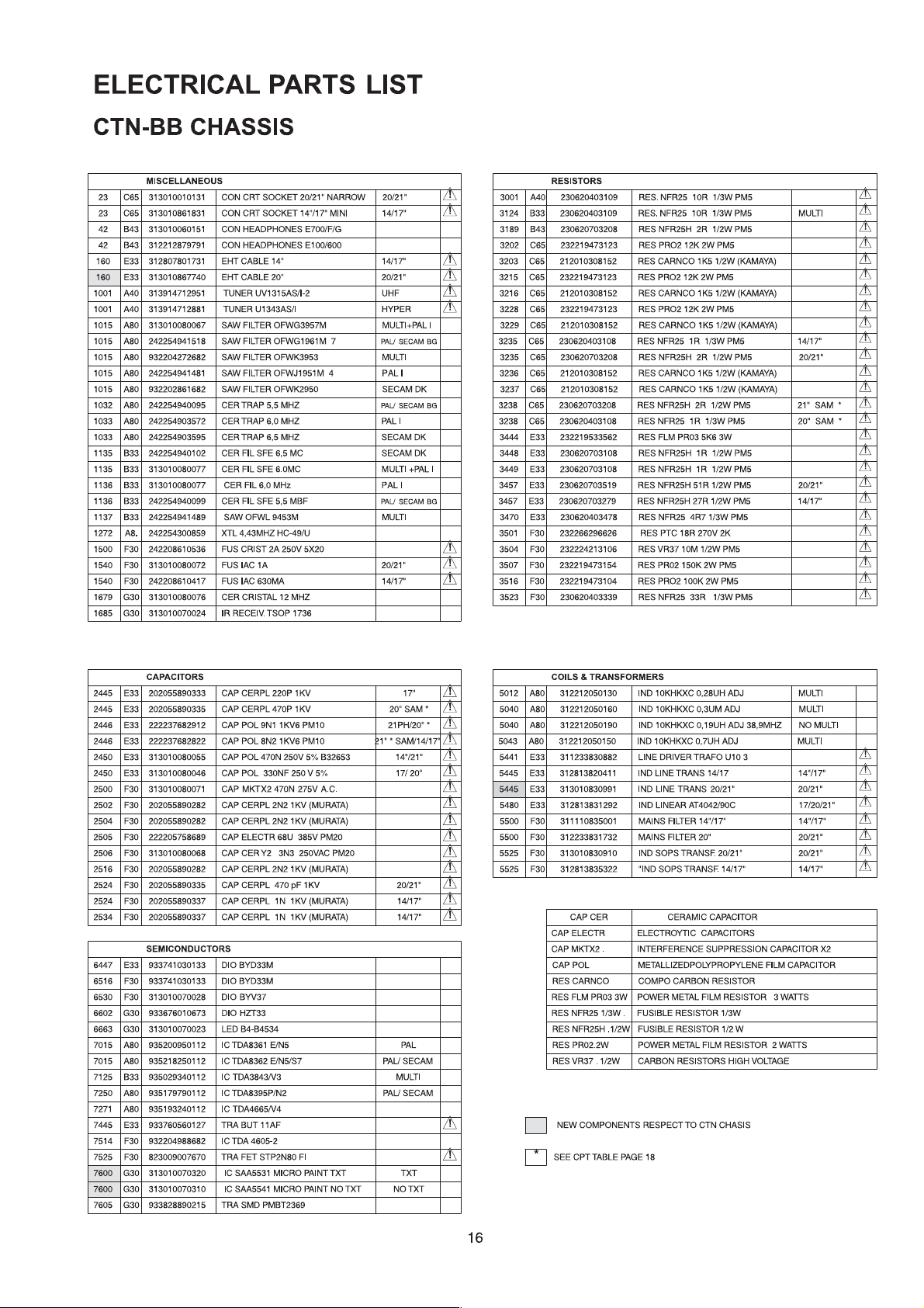
Service components 16 - 17 - 18
Introduction
The main change on this Chassis to the previous CTN-AA type are the introduction of
new Microprocessors for both - T ext and Non Text Models.
Also the Flyback Transformer for 20″ ONL Y MODELS has been changed.
The relevant Circuit Diagrams and PCB Layouts have been amended to show these
changes, plus minor corrections/updates have been made to all other circuit information
where this has been found necessary .
Page 16, 17 and 18 shows different Part Numbers for the Component changes on the
new chassis.
Please use the original CTN Service Manual for all other parts information.
2
Page 3

3284 M4
3285 M4
3286 M5
3289 M5
3290 K5
3291 K5
3292 K5
3340 B8
3341 B8
3342 B9
3345 D7
3350 C7
3351 A7
3353 B7
3354 B7
3370 D7
3371 D8
3372 D8
3841 J7
3843 J7
3845 K7
3848 L7
3850 I8
3851 I7
3852 J8
3853 J7
3854 I8
3855 K7
3858 L7
3860 I7
3862 L7
3865 L7
3871 M8
3875 L8
3876 M8
3879 J8
3880 J9
3881 J8
3882 K8
3883 K8
3884 M7
5001 F6
5010 B5
5012 B3
5015 G2
5032 E3
5040 C2
5043 B2
6001 F6
6014 A3
6020 B5
6042 B2
6275 L1
6289 L5
6372 D8
6849 L7
7001 F6
7015 D4
7016 F1
7030 E2
7250 H2
7271 K1
7875 M8
7876 J9
7877 K8
9001 G8
9002 H7
9003 F6
9004 E6
9005 F6
9012 A4
9015 G9
9016 G2
9017 D7
9020 G3
9021 G3
9034 F2
9035 M8
9043 A2
9051 E5
9080 G6
9115 A4
9124 G2
9261 M3
9262 K6
9265 G2
9271 J3
9289 M5
9331 D7
9354 M1
9366 A8
9367 C8
9370 C7
9371 C7
9372 D8
9600 F6
9810 L8
9812 K9
1M7 M5
2M7 M4
3M7 M4
4M7 M3
5M7 M3
1001 F7
1015 C4
1032 E3
1033 E4
1272 I5
2001 G6
2002 H7
2003 F6
2005 G8
2006 G8
2007 F2
2010 B4
2011 B4
2013 B4
2014 A3
2015 F5
2016 F5
2017 B5
2018 C5
2019 G1
2022 D6
2025 D5
2030 E2
2034 E4
2037 E2
2041 B2
2043 B2
2044 A2
2045 D2
2050 G3
2053 E4
2080 G5
2082 G5
2084 G5
2261 J5
2262 J5
2265 I5
2267 I3
2268 I3
2271 I1
2272 J2
2273 J2
2274 K1
2275 L1
2279 L3
2280 L3
2284 M4
2285 M4
2286 M5
2291 K6
2292 K6
2293 K6
2297 H1
2340 B9
2350 A8
2351 A7
2354 A7
2366 B9
2370 C7
2371 C7
2850 I8
2852 I8
2856 I9
2860 H7
2876 M8
3000 F8
3001 E6
3002 E7
3003 E7
3004 E8
3005 F7
3006 E9
3007 F9
3008 F9
3010 B4
3011 B3
3012 B4
3013 E6
3017 C5
3018 C5
3019 B5
3020 C4
3021 E5
3022 E5
3023 E6
3026 E8
3029 E3
3030 E2
3031 E3
3032 E3
3033 F4
3043 B2
3044 A2
3045 D2
3049 B3
3051 E5
3260 I5
3261 M3
3262 J5
3272 J1
3273 J1
3275 L1
3280 H3
3
Page 4

3216 D6
3217 D6
3218 C7
3219 D6
3220 D5
3221 D6
3222 E 6
3224 E 7
3225 E 7
3226 F7
3227 E 7
3228 E 6
3229 E 6
3230 F6
3232 D7
3233 F6
3234 F5
3236 E 4
3237 E 4
3244 F6
5101 I7
5235 E 4
6115 I8
6116 J8
6170 L 8
6205 B 6
6218 D6
6227 E 6
7015 L 7
7114 J2
7115 J1
7125 I7
7126 J8
7127 J8
7140 J3
7170 M8
7187 L 4
7205 B 6
7210 B 7
7211 D7
7212 E 7
7218 D6
7225 F7
7227 E 6
9110 J4
9111 J2
9112 J1
9114 K 6
9125 J5
9143 L 5
9156 I2
9157 I3
9183 L 4
9190 L 3
9191 L 3
9191 M2
9192 J3
9201 E 7
9202 C7
1L1 C8
1L2 F5
1M3 M2
2L1 D8
2L2 F4
2M3 L2
3L1 D8
3L2 F4
3M3 L2
4L1 B8
4L2 F4
5L1 B8
L3 F3
L4 C4
42 L1
1135 L 8
1136 L 8
1137 J7
1990 D3
2101 I8
2109 J1
2112 K 6
2117 K 8
2124 I6
2125 I6
2126 J7
2127 J6
2128 J6
2143 L 8
2152 M6
2155 M6
2156 H2
2169 L 8
2170 M8
2180 M7
2184 L 4
2185 L 4
2187 K 3
2188 K 3
2189 M4
2191 L 2
2192 L 2
2202 B 7
2204 C6
2206 F5
2217 D6
2230 F6
2237 F4
3111 J2
3112 J2
3114 J2
3115 J2
3117 J8
3118 I8
3119 I8
3120 J8
3121 J8
3124 H6
3125 J5
3126 J5
3143 L 8
3144 L 7
3151 L 7
3152 M6
3155 H4
3156 I4
3170 M8
3171 M8
3173 L 8
3184 L 5
3185 L 5
3189 K 4
3191 K 2
3194 L 2
3202 B 6
3203 B 6
3204 C6
3205 B 7
3206 C6
3207 C5
3208 C6
3210 C7
3211 D7
3212 E 7
3213 B 7
3214 D7
3215 D6
4
Page 5

3509 B5
3510 D5
3512 D4
3513 D4
3516 E3
3517 D5
3518 D5
3519 B4
3520 B4
3521 E5
3523 D4
3524 B4
3525 B4
3527 E5
3528 E4
3540 F5
3570 F4
3571 F4
3573 G4
3574 F4
3576 F5
3577 F5
5441 I5
5443 K5
5445 K3
5447 J3
5449 K5
5480 I4
5500 C3
5525 E3
5532 F5
5534 F3
5540 F5
5541 F6
5550 D6
5552 E4
6416 I2
6417 H2
6440 H6
6443 L5
6447 J5
6449 L6
6451 I4
6470 J3
6502 D3
6503 D3
6504 D3
6505 D3
6515 D5
6516 E3
6521 D6
6530 F3
6540 F5
6570 F4
6571 F4
7400 H2
7440 H5
7445 J5
7514 C4
7525 E4
7571 F5
7575 F4
9400 J2
9460 L4
9480 I4
9506 E6
9523 D4
9524 C5
9560 G5
9561 G6
1M1 A3
1M2 C2
1M5 J4
1M6 I3
2M1 A2
2M2 C2
2M6 J5
3M6 J5
4M5 J4
4M6 L4
5M5 K2
6M5 J2
22 B3
47 J2
47 J4
49 C3
1500 A2
2401 I1
2402 J2
2404 K2
2405 L2
2414 H2
2415 I2
2416 J2
2440 H5
2442 I5
2443 L5
2444 H5
2445 J5
2446 K5
2448 J3
2449 J3
2450 I4
2451 I4
2453 L6
2458 J3
2460 L4
2463 L5
2470 I3
2500 B3
2502 D3
2504 D3
2505 D4
2506 B6
2508 E5
2509 B4
2510 D5
2511 D5
2514 D6
2515 D5
2516 D3
2520 D5
2523 B5
2524 E4
2530 F3
2532 F5
2534 F2
2540 F6
2561 G4
2562 G4
3235 J5
3238 J5
3400 K1
3401 K2
3402 J1
3403 K2
3404 L2
3405 L2
3406 L2
3407 L2
3408 H2
3410 L2
3411 L2
3412 K2
3415 J2
3416 J2
3440 H5
3441 H6
3442 I6
3444 H5
3445 I5
3448 K5
3449 K5
3451 I4
3455 H4
3456 H4
3457 J3
3460 L4
3470 J3
3480 I4
3501 C3
3504 A3
3507 B5
3508 D5
5
Page 6
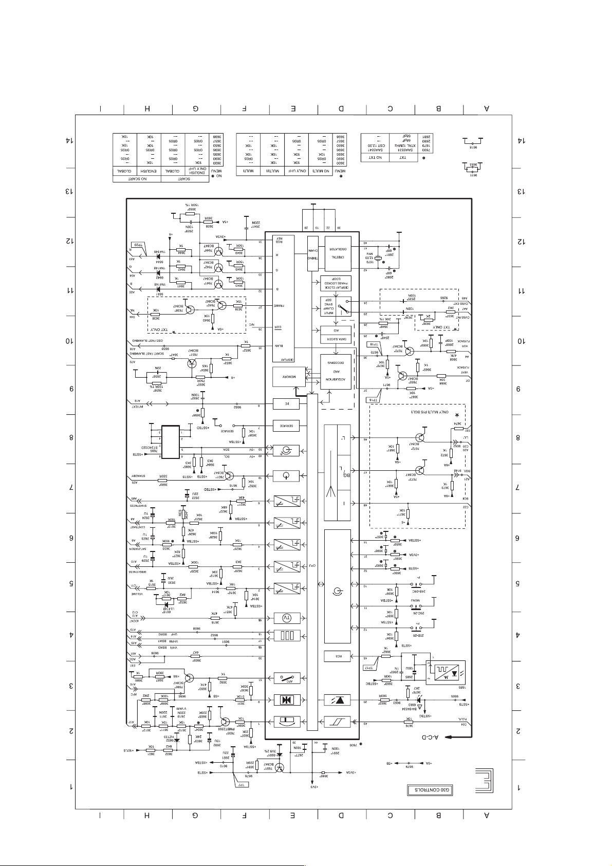
3657 C6
3658 G12
3659 G13
3660 C3
3661 C7
3662 C4
3663 C3
3664 B9
3665 B9
3667 C9
3668 B10
3669 B10
3670 C9
3671 C6
3672 B8
3673 B7
3674 B8
3675 C3
3676 C2
3680 H7
3681 C8
3682 F7
3684 G7
3685 G7
3686 H3
3687 H3
3688 H3
3689 H3
3690 C5
3691 F1
3692 F3
3693 G3
3694 C4
3695 C6
3696 C6
3697 C4
3698 G9
3699 C5
6602 G2
6616 H5
6641 H11
6642 H11
6644 H12
6663 B3
6691 E2
7600 D2
7601 F7
7605 F2
7638 G11
7640 G11
7641 G11
7642 G11
7644 G12
7651 G10
7665 C9
7670 C10
7672 B8
7673 B7
7685 H8
7686 G3
7691 E1
9052 B8
9148 B7
9266 B11
9609 H4
9610 F1
9611 A13
9614 G5
9616 F7
9618 A14
9650 H10
9651 F4
9652 G4
9653 A13
9658 G4
9663 C3
9665 B3
9670 C10
9671 C9
9678 F1
9679 C1
9686 G3
9692 F9
B3
1679 C12
24B-24C B5
25B-26 B4
25C-26 B5
2602 G2
2610 G2
2611 H2
2622 G7
2623 H6
2624 H6
2629 H6
2630 H5
2635 C11
2636 C11
2641 F12
2648 C10
2651 F2
2656 H9
2659 G12
2660 C3
2669 B10
2677 E2
2680 C11
2681 C12
2685 C3
2691 D2
2692 G9
3600 C5
3601 H2
3602 H2
3603 G2
3604 G2
3605 G2
3606 F2
3607 F2
3608 F8
3609 G4
3610 G2
3611 H2
3612 H2
3613 H6
3614 F5
3615 H5
3616 F5
3617 H5
3618 G4
3619 F5
3620 F5
3621 F7
3622 F7
3623 G6
3624 G6
3625 F6
3626 G6
3627 G6
3628 F6
3629 G5
3630 F3
3631 F3
3632 G5
3633 H6
3636 B10
3637 B11
3638 H11
3639 F11
3640 G10
3641 G11
3642 G11
3643 F11
3644 G12
3645 F11
3646 D1
3647 G10
3648 C10
3649 F12
3650 C6
3651 F4
3652 F10
3653 F10
3654 G9
3655 G9
3656 H9
6
Page 7
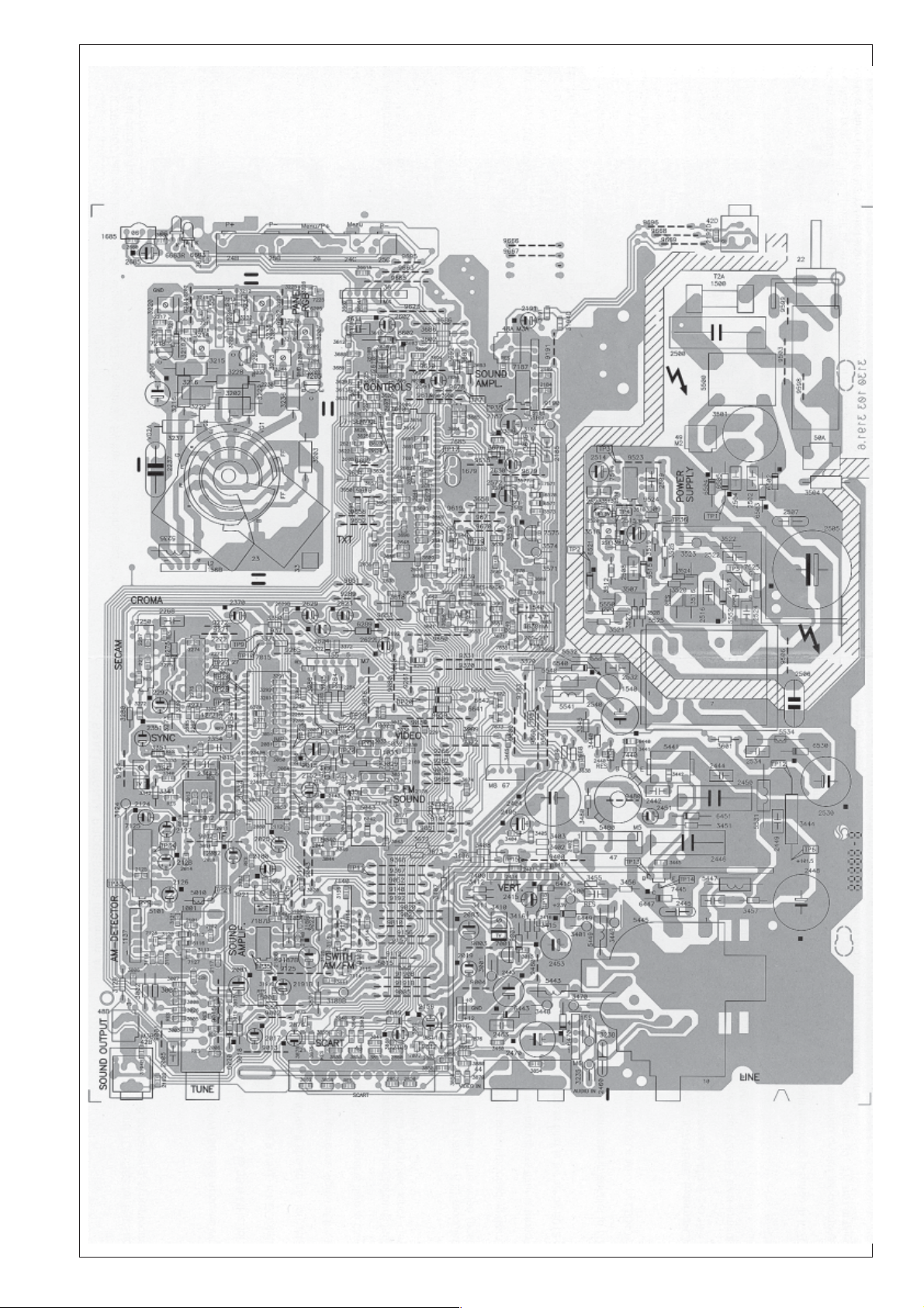
OUTOUT
OUTOUT
OUT
YY
YY
Y
ARD LAARD LA
ARD LAARD LA
ARD LA
PRINT BOPRINT BO
PRINT BOPRINT BO
PRINT BO
7
Page 8
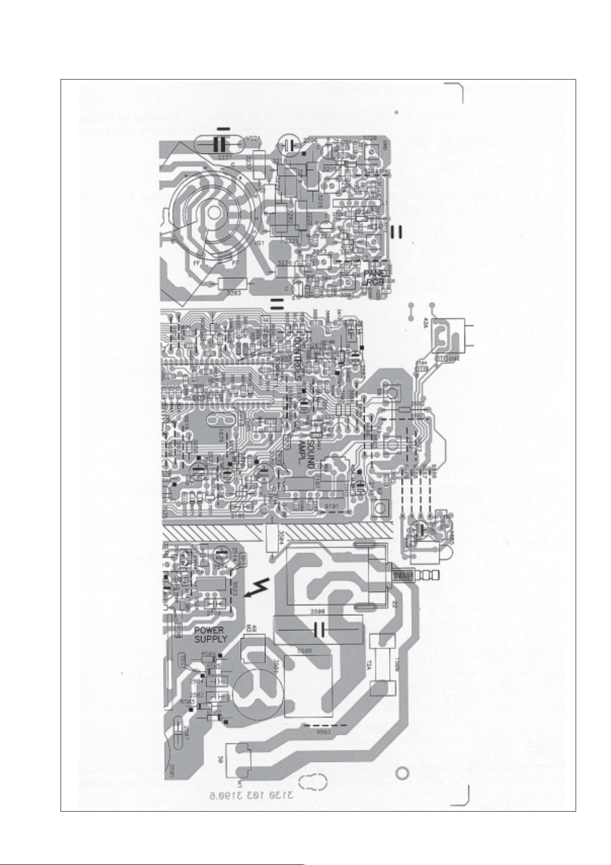
PRINT BOPRINT BO
PRINT BO
PRINT BOPRINT BO
ARD LAARD LA
ARD LA
ARD LAARD LA
YY
OUTOUT
Y
OUT
YY
OUTOUT
8
Page 9

CIRCUIT DESCRIPTIONCIRCUIT DESCRIPTION
CIRCUIT DESCRIPTION
CIRCUIT DESCRIPTIONCIRCUIT DESCRIPTION
1.- SMALL SIGNAL PROCESSING (Diagram A)1.- SMALL SIGNAL PROCESSING (Diagram A)
1.- SMALL SIGNAL PROCESSING (Diagram A)
1.- SMALL SIGNAL PROCESSING (Diagram A)1.- SMALL SIGNAL PROCESSING (Diagram A)
The small signal is processed by TDA8361, (TDA8360 no scart) for Pal sets and TDA8362 for Pal/Secam
sets (IC 7015), including IF detection, video processing, chroma decoder, RGB processing, sync processor
and FM sound decoder.
1.1- IF detection (IC7015/6A)
- IF input (pins 45,46)- IF input (pins 45,46)
- IF input (pins 45,46): The IF signal comes from pin 11 of the tuner to the IF SA W (Surf ace Acoustic W av e)
- IF input (pins 45,46)- IF input (pins 45,46)
filter (1015) and the IF-detector IC7015/6A (pins 45 and 46).
- IF filter (1015): The IF bandpass characteristic, determined by the SAW filter, is 33.4 to 38.9 MHz. for BG
sets, 33.5 to 39.5 MHz. for PAL I sets and 32.4 to 38.9 MHz. for DK sets.
- IF oscillator (pins 2,3)- IF oscillator (pins 2,3)
- IF oscillator (pins 2,3): Carrier frequency, present in coil L5040, is tuned at 38.9 MHz. for BG sets or
- IF oscillator (pins 2,3)- IF oscillator (pins 2,3)
39.5 MHz for Pal I sets
- A- A
GC vGC v
- A
- A- A
for 1mV. antenna signal by means of R3021 (pin 49).
- AFC signal (pin 44):- AFC signal (pin 44):
- AFC signal (pin 44): The Automatic Frequency Control is obtained from the reference signal of the IF-
- AFC signal (pin 44):- AFC signal (pin 44):
detector. C2037 smoothes the AFC voltage.
- Identification (pin 4)- Identification (pin 4)
- Identification (pin 4): The identification output is applied to pin 16 of the µC. This signal is high in case of
- Identification (pin 4)- Identification (pin 4)
signal detected.
--
Video output (pin 7)Video output (pin 7)
-
Video output (pin 7) : This baseband CVBS signal with 2Vpp of nominal amplitude, also contains the FM
--
Video output (pin 7)Video output (pin 7)
intercarrier sound signal. Sound is filtered out by a ceramic trap (1032 or 1033) which frequency can be
different depending on the system: 5.5 MHz. for BGLL’, 6.0 MHz. Pal I or 6,5 MHz. for DK.
oltage (pin 47):oltage (pin 47):
GC v
oltage (pin 47): The AGC dela y ed v oltage is applied to pin 1 of the tuner. It should be adjusted
GC vGC v
oltage (pin 47):oltage (pin 47):
Multistandard sets
-The IC TDA8362 changes automatically between negative (BGIDK) and positive (LL’) modulation.
The IC also determines if the AGC circuit should control at the top white level of the video (positive
modulation) or at the top sync level (negative modulation).
-Saw filter (1015) bandpass characteristic is modified by BG/L switching signal proceeding from the
microcontroller:
- For BGIDK reception BG/L is low, D6014 does no conduct and the bandpass filter is tuned by
5012 and 2013 at 32.9MHz. to 38,9 MHz.
- For LL’ reception BG/L is high, D6014 conducts and so the bandpass filter is tuned b y 5012 and
C2014 at 32.4 to 38.9 MHz.
-Oscillator frequency is controlled by the L/L’ switching signal:
-For BGIL reception L/L’ is lo w, D6042 conduct and so coil 5043 is connected in parallel to 5040.
- The circuit is tuned to 38.9 MHz.
- For L’ reception L/L’ is high, D6042 does nor conduct and the circuit is tuned to 33.4 MHz. by L5040 only.
1.2- Source select, luminance and chroma separation (IC7015/6B)
- Source select (pin 13, 15, 16)- Source select (pin 13, 15, 16)
- Source select (pin 13, 15, 16): The internal CVBS signal is now f ed to pin 13 IC7015/6B. External CVBS
- Source select (pin 13, 15, 16)- Source select (pin 13, 15, 16)
from the pin 20 of Euroconnector is present on pin 15. The source selector s witch between internal (pin 16 = 0V .)
or external (pin 16 = 8V.).
- Luminance and chrominance separation- Luminance and chrominance separation
- Luminance and chrominance separation: Chrominance signal is filtered out (-20dB) by a luminance
- Luminance and chrominance separation- Luminance and chrominance separation
notch filter which is internally calibrated at the subcarrier frequency (4.43MHz).
1.3- Chroma Decoding (IC7015/6C)
Pal or Secam signals are recognized automatically by the IC. For Pal signals decoding is made in IC7015/
6C and for Secam signals in IC7250 (TDA8395).
- P- P
al signalal signal
- P
al signal: This signal is amplified and demodulated. The 4.43 MHz. reference crystal for chrominance
- P- P
al signalal signal
demodulation is present at pin 35 of IC7015/6C. The R-Y and B-Y out-puts (pins 30, 31) are applied to
chroma delay line IC7221 (TD A4665).
- Secam signal (pin 27)- Secam signal (pin 27)
- Secam signal (pin 27): This signal is applied to pin 16 of Secam decoder IC7250.
- Secam signal (pin 27)- Secam signal (pin 27)
9
Page 10

- Secam ref- Secam ref
- Secam ref
- Secam ref- Secam ref
erence (pin 32)erence (pin 32)
erence (pin 32): Pal or Secam signals are recognized using a DC level by bi-directional
erence (pin 32)erence (pin 32)
communication line between this pin and pin 1 of IC7250.
-If IC7015/6C has detected a Pal signal, Vpin 32 is made 1,5V. By then the demodulated R-Y and BY outputs (pins 30, 31) are applied to delay line IC7271.
-If IC7015/6C has not detected a Pal signal, Vpin 32 is made 5V. By then the demodulated R-Y and
B-Y at outputs (pins 30, 31) are not used.
-If IC7250 has detected a Secam signal, Vpin 1 IC7250 becomes lo w, sinking typical 150µA. current
from pin 32 (5V.) of IC7015/6C, which one detect this current to know that a Secam signal has been
detected. In this case R-Y and B-Y signals are applied to the delay line IC7271 via outputs of
IC7250 (pins 9 and 10).
This bi-directional communication line uses AC level to calibrate the 4,43MHz. between the PLL and chroma
cloche filter of IC7250.
1.4- RGB-dematrixing(IC7015/6D)
- R-Y- R-Y
, B-Y inputs (pins 28, 29), B-Y inputs (pins 28, 29)
- R-Y
, B-Y inputs (pins 28, 29): The R-Y and B-Y signals come from delay line (IC7271) and the Y signal
- R-Y- R-Y
, B-Y inputs (pins 28, 29), B-Y inputs (pins 28, 29)
comes (internally) from IC7015/6B.
The sandcastle pulse coming (internally) from the IC7015/6E (pin 38) synchronizes RGB dematrixing and
suppresses the RGB signals during line and frame flyback.
--
Video controls (pins 17, 25, 26)Video controls (pins 17, 25, 26)
-
Video controls (pins 17, 25, 26): These inputs for contrast, brightness and saturation can be adjusted
--
Video controls (pins 17, 25, 26)Video controls (pins 17, 25, 26)
from 0,5V to 4,5V by the µC. If beam current is limited reducing contrast with D6289 circuit.
- RGB inputs (pins 22, 23, 24)- RGB inputs (pins 22, 23, 24)
- RGB inputs (pins 22, 23, 24): External RGB inputs come from Euroconnector and are switched by fast
- RGB inputs (pins 22, 23, 24)- RGB inputs (pins 22, 23, 24)
blanking.
- F- F
ast bast b
- F
- F- F
lanking (pin 21)lanking (pin 21)
ast b
lanking (pin 21): W hen voltage of pin 21 is 0,4V. internal RGB is used. F or a pin 21 voltage between
ast bast b
lanking (pin 21)lanking (pin 21)
0,4V. and 3,5V. the set switch to external RGB.
If voltage of pin 21 is 4V. both internal and external are deleted. The up uses this status to insert RGB signals
from OSD generator directly to RGB outputs.
Fast blanking can switch signals for full screen (by a DC voltage) or for a part of the screen (by a pulse
voltage).
- RGB outputs (pins 18, 19, 20)- RGB outputs (pins 18, 19, 20)
- RGB outputs (pins 18, 19, 20): See RGB amplifier .
- RGB outputs (pins 18, 19, 20)- RGB outputs (pins 18, 19, 20)
1.5- Horizontal synchro (IC7015/6E)
- Star- Star
t up (pin 36)t up (pin 36)
- Star
t up (pin 36): When the set is switched on, v oltage at pin 36 rises and when exceeds 7V. the horizontal
- Star- Star
t up (pin 36)t up (pin 36)
oscillator starts running at approx. 25 KHz. (slow start). After the line starts, main supply of IC7015 (pin 10)
comes up to 8V. and the line frequency changes to 15625 Hz.
StandbStandb
-
Standb
StandbStandb
y (pin 36)y (pin 36)
y (pin 36): This pin is used also for standby function. In this case the voltage is reduced to 3V. by
y (pin 36)y (pin 36)
the uP and so the line is shut down.
- Hor- Hor
..
oscillator oscillator
- Hor
.
oscillator: Thi s oscillator is fully integrated and internally calibrated. F requency is obtained derived of
- Hor- Hor
..
oscillator oscillator
chroma oscillator on pin 35 of IC7015/6C.
- Hor- Hor
..
sync separ sync separ
- Hor
.
sync separ
- Hor- Hor
..
sync separ sync separ
- Oscillator synchro (pin 40)- Oscillator synchro (pin 40)
- Oscillator synchro (pin 40): Oscillator is synchronized with video signal by a first control loop circuit. The
- Oscillator synchro (pin 40)- Oscillator synchro (pin 40)
atorator
ator: This circuit (fully integrated) separates hor. pulses of CVBS proceeding from 7051/6B.
atorator
control voltage is present at pin 39.
- Hor- Hor
..
phase control (pin 39) phase control (pin 39)
- Hor
.
phase control (pin 39): Line fly-back (pin 38) is synchronized with oscillator b y a second control loop
- Hor- Hor
..
phase control (pin 39) phase control (pin 39)
circuit. The control voltage is present at pin 39. Phase can be adjusted by 3354.
- Hor- Hor
..
output (pin 37) output (pin 37)
- Hor
.
output (pin 37): Oscillator is converted in square wave voltage at this pin.
- Hor- Hor
..
output (pin 37) output (pin 37)
Sandcastle (pin 38)Sandcastle (pin 38)
-
Sandcastle (pin 38): This pin is used as line fly-back input and also as sandcastle output. Levels of
Sandcastle (pin 38)Sandcastle (pin 38)
sandcastle pulse are 5,3V for burst detection, 3V. for line b lanking and 2V. f or fr ame blanking.
1.6- Vertical synchro (IC7015/6E)
--
VV
erer
tical oscillator (pin 42)tical oscillator (pin 42)
-
V
er
tical oscillator (pin 42): Frequency is obtained dividing frequency of chroma oscillator on pin 35
--
VV
erer
tical oscillator (pin 42)tical oscillator (pin 42)
IC7015/6C. At pin 42 a sawtooth signal is present. Resistor 3342 is used to correct vertical amplitude with
beam current.
--
VV
erer
t.t.
sync. sync.
-
V
er
t.
--
VV
erer
t.t.
--
VV
erer
t.t.
-
V
er
t.
--
VV
erer
t.t.
--
VV
erer
t.t.
-
V
er
t.
--
VV
erer
t.t.
separ separ
sync.
separ
sync. sync.
separ separ
dr dr
iviv
e (pin 43)e (pin 43)
dr
iv
e (pin 43): This out-put is used to drive the vertical amplifier (7400)
dr dr
iviv
e (pin 43)e (pin 43)
f f
eedbaceedbac
f
eedbac
f f
eedbaceedbac
atorator
ator: I t separates fr ame sync. pulses from CVBS and so synchronizes frame oscillator .
atorator
k (pin 41)k (pin 41)
k (pin 41): this f eedback is proportional to deflection current and is used to correct the vert.
k (pin 41)k (pin 41)
drive signal.
10
Page 11

2.- RGB AMPLIFIERS (diagram B)2.- RGB AMPLIFIERS (diagram B)
2.- RGB AMPLIFIERS (diagram B)
2.- RGB AMPLIFIERS (diagram B)2.- RGB AMPLIFIERS (diagram B)
- RGB inputs- RGB inputs
- RGB inputs : The RGB signals a vailable at pins 20, 19 and 18 of IC7015/6D are drived b y emitter followers
- RGB inputs- RGB inputs
(7210, 7211, 7212), to RGB amplifiers.
- Ref- Ref
- Ref
- Ref- Ref
erence verence v
erence v
erence verence v
oltage (7225)oltage (7225)
oltage (7225): An internal reference voltage of 2.5V. is produced on the emitter of transistor
oltage (7225)oltage (7225)
7225 to keep the black level stable.
- RGB amplifiers (7205, 7218, 7227)- RGB amplifiers (7205, 7218, 7227)
- RGB amplifiers (7205, 7218, 7227): Signal is inverted and dr ived to the CPT by RGB amplifiers. To
- RGB amplifiers (7205, 7218, 7227)- RGB amplifiers (7205, 7218, 7227)
improve high frequency amplification there are small capacitors (2204, 2217 and 2230).
- Flash-o- Flash-o
- Flash-o
- Flash-o- Flash-o
vv
er protectionser protections
v
er protections: Clamping diodes to +8V. (6203, 6216, 6229) and 1K5 series resistors (3203,
vv
er protectionser protections
3216, 3229) are added for protect the circuit from CPT flash-over.
--
White adjustmentWhite adjustment
-
White adjustment: The gain of B and G amplifiers can be adjusted by 3213 and 3214.
--
White adjustmentWhite adjustment
- Cut-off adjustment- Cut-off adjustment
- Cut-off adjustment: The black level of the CPT can be adjusted by 3207, 3220, 3234 and Vg2.
- Cut-off adjustment- Cut-off adjustment
3.- SOUND CIRCUIT (diagram C)3.- SOUND CIRCUIT (diagram C)
3.- SOUND CIRCUIT (diagram C)
3.- SOUND CIRCUIT (diagram C)3.- SOUND CIRCUIT (diagram C)
3.1- FM Sound detection (IC7015/6F)
- FM input (pin 5)- FM input (pin 5)
- FM input (pin 5): FM sound is extracted from baseband video (CVBS) proceeding of IF detector and
- FM input (pin 5)- FM input (pin 5)
filtered through 1136 (5.5 MHz. for BG sets, 6.0 Mhz. for Pal I sets, 6.5 Mhz. for DK sets).
- FM demodulation- FM demodulation
- FM demodulation: FM - mono sound demodulation takes place in IC7015/6F. No adjustment is required
- FM demodulation- FM demodulation
because demodulation is doing by an automatic PLL (4.2 to 6.8 MHz.).
- De-emphasis (pin 1)- De-emphasis (pin 1)
- De-emphasis (pin 1): Sound frequency characteristic is defined by de-emphasis capacitor C2112 at pin 1.
- De-emphasis (pin 1)- De-emphasis (pin 1)
- Exter- Exter
- Exter
- Exter- Exter
nal FM audio out (pin 1)nal FM audio out (pin 1)
nal FM audio out (pin 1): The signal at this pin is amplified by T7114 and T7115 to drive the
nal FM audio out (pin 1)nal FM audio out (pin 1)
euroconnector sound outputs (pins 1,3).
- External FM audio in (pin 6)- External FM audio in (pin 6)
- External FM audio in (pin 6): External audio proceeding of euroconnector (pins 2,6) is applied to this pin.
- External FM audio in (pin 6)- External FM audio in (pin 6)
Selection between internal or external is done by pin 16 of IC7015/6B.
This output is drived to pin 3 of the final sound amplifier IC7187 (TDA7052 or TDA7056).
Multistandard sets:
-FM demodulation: This function is done in the same wa y that no multi sets. The only diff erence consist
of a second Pal I 6MHz. filter (1135) in addition to the 5,5MHz. BG filter (1136). 6MHz. filter is switched
off for BG reception by transistor 7170 depending on BG/I signal.
-AM demodulation: In Multistandard sets, also AM demodulation for LL’ systems is necessary. AM
sound is extracted directly from the tuner instead of from baseband video.
AM Sound detection (IC7125)
- AM input (pins 1,16): AM signal at 32,4MHz. for L system or 39,9MHz. for L’, is removed from IF
signal coming from tuner by SA W filter 1137 (double band pass char acteristic). Sound is switched by
T7126, D6115, TS7127 and D6116 depending on L/L’ signal: For L’ reception (L/L’ is high) IF signal is
present at pin 1, and For L reception, IF signal is present at pin 2.
The required frequency spectrum is fed to pins 1 and 16 of the AM demodulation IC7125.
- AGC (pin 3,5): C2126 and 2127 are AGC related storage capacitors.
- AM Sound output (pin 6): The demodulated signal at pin 6 of IC7125 is supplied to the source selection
switch (pins 1, 5 IC 7140).
AM Sound switching (IC7140)
- External audio out (pin 15): Audio out is selected between AM sound (pin1) or FM sound (pin2) by
internal switch depending on BG/L signal (pin 10).
- Audio in (pins 3, 4, 5): Top switch in IC7140 select between internal AM sound (pin 5) and EXT sound
from SCART (pin3) by INT/EXT signal (pin 9). The output of this selector (pin 4) is f ed to input pin 6 of
FM demodulator (IC7015/6F).
- Internal AM audio switching (pin 13): This pin is switched to 8V when the set is in L or L’ system (AM
sound). Then, pin 1 of IC7015/6F is 8V. and this IC s witches internally its sound input from pin 5 to pin
6, where AM sound is present. (Sound proceeding from pin 4 of IC7140 can be internal AM or external).
11
Page 12

3.2- Sound amplifier (IC7187)
Sound amplifier can be TD A7052 f or 14" and 17" models or TDA7056 f or 20" and 21" models .
Amplified sound is drived to the headphones output and loudspeakers. If headphones are connected, loudspeakers
are switched off.
Volume control on DC level is present at pin 4 for TD A7052 or pin 5 for TDA7056.
4.- PO4.- PO
4.- PO
4.- PO4.- PO
WER SUPPLWER SUPPL
WER SUPPL
WER SUPPLWER SUPPL
Y (DiagY (Diag
Y (Diag
Y (DiagY (Diag
rr
am D)am D)
r
am D)
rr
am D)am D)
Mains isolated switched mode power supply (SMPS), controlled b y IC7514 (TDA4605) in v ariable frequency
mode.
- Switching beha- Switching beha
- Switching beha
- Switching beha- Switching beha
viourviour
viour: The switching period is divided in on-time, when energy is extracted from the
viourviour
mains into the primary winding (8-12 of 5525), off-time, when energy in the transformer is supplied to the
loads via secondary windings of 5525 and dead when no energy is extracted or supplied.
- Standb- Standb
- Standb
- Standb- Standb
y modey mode
y mode: Output voltages are present when the set is on stand by, due to standby is done cutting
y modey mode
line deflection. On-time is lo w er and power consumption is very low.
4.1- Primary side
- Degaussing- Degaussing
- Degaussing: R3501 is a dual PTC (2 PTC’s in one housing). After switch on set, PTC is cold so low-
- Degaussing- Degaussing
ohmic and so degaussing current is very high. After degaussing, PTC is heated so high-ohmic, so in
normal operation degaussing current is very low.
- Rectifier- Rectifier
- Rectifier: Mains voltage is filtered by L5500, full wave rectified by diodes D6502-D6503-D6504-D6505
- Rectifier- Rectifier
and smoothed by C2505 (300V. DC for 220V AC mains).
4.2- Control circuit (IC7514)
- Star- Star
t up and supply (pin 6)t up and supply (pin 6)
- Star
t up and supply (pin 6): When the set is switched on, a current via R3507 is applied to pin 6. When
- Star- Star
t up and supply (pin 6)t up and supply (pin 6)
C2514 is charged to 15V. the power supply starts and a current from pin 5 to T7525 is drived. T7525 and
starts conduction and a voltage across transformer windings is built up. The voltage across winding 4-2 is
rectified by diode D6521 and used to supply the IC on pin 6.
- Soft star- Soft star
- Soft star
- Soft star- Soft star
t (pin 7)t (pin 7)
t (pin 7): The capacitor C2523 causes a slow increase of the duration of the output pulse during
t (pin 7)t (pin 7)
start up.
- IC output (pin 5)- IC output (pin 5)
- IC output (pin 5): This output drives T7525. R3523 is a fuse resistor to protect IC from short circuits in
- IC output (pin 5)- IC output (pin 5)
T7525. D6516 limits the maximum voltage in T7525.
- Star- Star
t conduction of t conduction of
- Star
t conduction of
- Star- Star
t conduction of t conduction of
T7525 (pin 8)T7525 (pin 8)
T7525 (pin 8): A voltage proceeding from winding 4-2 is applied to this pin. The zero
T7525 (pin 8)T7525 (pin 8)
crossing detector recognizes the complete discharge of the energy stored in the transformer core, in addition
to a dead time depending on C2508. This circuit guarantee that T7525 star ts conduction at minimum Vds
voltage (see signals 4.5 pag 13).
- Primary current info (pin 2)- Primary current info (pin 2)
- Primary current info (pin 2): Current primary winding is simulated by a pin 2 voltage.
- Primary current info (pin 2)- Primary current info (pin 2)
- Output v- Output v
- Output v
- Output v- Output v
oltage infoltage inf
oltage inf
oltage infoltage inf
o (pin 1)o (pin 1)
o (pin 1): The voltage across winding 4-2 is rectified by diode D6515, divided by
o (pin 1)o (pin 1)
R3527, R3518 and R3508 and applied to pin 1. Internal control voltage (Vcont) in versely proportional to V
pin 1 is generated. Tipical Vpin1 is 400 mV.
- Output regulation (pins 1, 2, 8)- Output regulation (pins 1, 2, 8)
- Output regulation (pins 1, 2, 8): IC7514 stabilizes output voltage b y controlling T-on and so the frequency
- Output regulation (pins 1, 2, 8)- Output regulation (pins 1, 2, 8)
and the duty cycle:
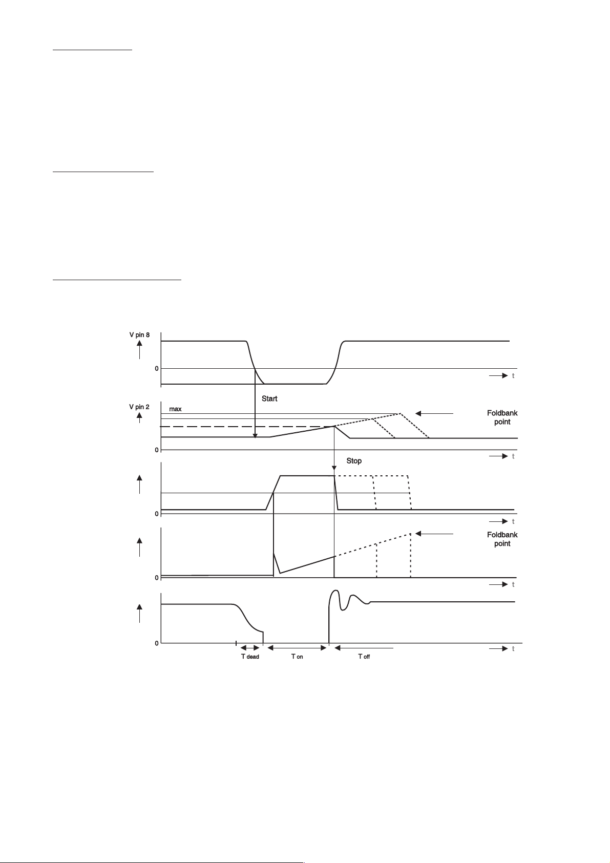
Start pulse to T7525 is determined by pin 8 circuit (see signals 4.5 page 13 ).
Then a sawtood voltage Vpin 2 is generated at pin 2. Stop pulse to T7525 is produced when Vpin 2
reaches Vcont.
Output control is done by the following way:
If output is higher, Vpin 1 is higher, Vcont is lower , T-on and output will be reduced.
If output is lower , output will be increased.
Output voltage of supply can be adjusted by R3518.
Mains voltage variation is stabilized in the following way:
If mains voltage is higher , slope in the sawtood voltage Vpin 2 is higher , stop point is reached before
and T-on is reduced.
If mains voltage is lower, T-on is increased.
12
Page 13
4.3- Protections
- Ov- Ov
erer
- Ov
- Ov- Ov
load protection (pin 2)load protection (pin 2)
er
load protection (pin 2): This is produced if T-on is increased till Vpin 2 voltage reaches the foldback
erer
load protection (pin 2)load protection (pin 2)
point (see signals 4.5). The IC will switch into overload mode (off and on continuously).
- Output v- Output v
- Output v
- Output v- Output v
oltage protections (pin 6)oltage protections (pin 6)
oltage protections (pin 6): Limiting values of Vpin 6 voltage (7.25 and 16V.) provide under and
oltage protections (pin 6)oltage protections (pin 6)
overvoltage protections for the circuit.
- Mains o- Mains o
- Mains o
- Mains o- Mains o
vv
erer
vv
oltage (pin 3)oltage (pin 3)
v
er
v
oltage (pin 3): The voltage at pin 3 IC7515 is a measure for the mains v oltage and so the DC
vv
erer
vv
oltage (pin 3)oltage (pin 3)
voltage across C2505. As soon as the voltage Vpin 3 reaches 6.6V. the supply will stop running.
4.4- Secondary side
- Line supply- Line supply
- Line supply: The value to adjust the supply is 101,5V. for 14" CPT’S, 102,5V. f or 17" CPT’S and 107V. for
- Line supply- Line supply
20"/21" CPT’S. This supply is also used to obtain the +33V. varicap voltage by D6602.
- A- A
- A
- A- A
uxiliaruxiliar
uxiliar
uxiliaruxiliar
y supply (+11Vy supply (+11V
y supply (+11V
y supply (+11Vy supply (+11V
.).)
.): This supply is used f or sound output amplifier, for start up the line circuitry and
.).)
for the stand by of the microprocessor. +5STB is regulated by T7525 and D6575. A +5V. power on reset
signal (POR) is obtained during start up by R3573 till T7571 conducts by D6570.
4.5- Power supply signals
V pin 5 = V pin 5 =
V pin 5 =
V pin 5 = V pin 5 =
V contV cont
V cont
V contV cont
V GS (7525)V GS (7525)
V GS (7525)
V GS (7525)V GS (7525)
I DS (7525)I DS (7525)
I DS (7525)
I DS (7525)I DS (7525)
V DS (7525)V DS (7525)
V DS (7525)
V DS (7525)V DS (7525)
13
Page 14

5.- DEFLECTION (Diagram E)5.- DEFLECTION (Diagram E)
5.- DEFLECTION (Diagram E)
5.- DEFLECTION (Diagram E)5.- DEFLECTION (Diagram E)
5.1- Frame deflection
This function is performed by the integrated circuit TDA3653 (7400).
- Frame supply (pins 6, 8, 9)- Frame supply (pins 6, 8, 9)
- Frame supply (pins 6, 8, 9): Pin 9 is used to supply the IC except output stage which one is supplied by
- Frame supply (pins 6, 8, 9)- Frame supply (pins 6, 8, 9)
pin 6. At pin 6 there is a higher voltage during flyback time. This is produced adding the flyback signal
present at pin 8 to a +25V. supply by D6416 and C2415. Pin 8 is also used to drive v ertical flyback input at
pin 37 of the up. (IC 7600)
--
VV
erer
tical input (pins 1, 3)tical input (pins 1, 3)
-
V
er
tical input (pins 1, 3): The input circuit is driven b y pin 44 of IC7015/6E. V ertical signal is amplified and
--
VV
erer
tical input (pins 1, 3)tical input (pins 1, 3)
inverted.
--
VV
erer
tical output (pin 5)tical output (pin 5)
-
V
er
tical output (pin 5): Vertical output is applied to deflection coil. DC current is suppressed b y C2404. A
--
VV
erer
tical output (pin 5)tical output (pin 5)
voltage proportional to current deflection is present in R3411/12 and a feedback of it is sent to pin 42 of
IC7015/6 by 3407, so that amplitude can be adjusted by 3410. DC feedback is present in R3406. Linearity
is corrected by the network around C2405.
--
TRC protection (pin 7TRC protection (pin 7
-
TRC protection (pin 7): When frame deflection is broken down, the tube is protected blanking all the
--
TRC protection (pin 7TRC protection (pin 7
picture by pin 7 output.
5.2- Line deflection
The final line transistor is driven by the transformer 5441, whose primary winding is driven by the transistor
T7440 connected to the line drive output of IC7015/6E.
The horizontal deflection stage is carried out in a conventional way, with the deflection transistor (T7445)
and line transformer (5545).
Beam current info (BCI) is present at C2460.
There are the following auxiliary supply voltages obtained from line transformer (5545):
+25V.: To supply frame deflection..
+12V.: To obtain +8V . by IC7016 (diagram A) for small signal, +5V. by T7001 (diagram A) for the tuner
and for the microcontroller .
6.- MICROCONTROLLER/TEXT (Diagram E)6.- MICROCONTROLLER/TEXT (Diagram E)
6.- MICROCONTROLLER/TEXT (Diagram E)
6.- MICROCONTROLLER/TEXT (Diagram E)6.- MICROCONTROLLER/TEXT (Diagram E)
The CTN-BB chassis is designed to accept 2 different microcontrollers: SAA5531 and SAA5541.
Both microcontrollers are mounted in the same position (7600), and the associated circuitry is the same.
The ROM of the ICs contain an specific program that assures all the functions of the appliance, including a
MENU to control the set is (see Instructions Manual).
For no TXT sets SAA5541 is used.
For TXT sets SAA5531 is used which one also contains a teletext decoder , including the follo wing functions:
TXT on/off, reveal, freeze, temporary cancellation, clock, subcode, zoom, index, flof, page +/-, X/26 and 8/
30 packet decoding (station identification and start-up page).
Following there is an explanation of the different functions of the microcontroller indicating pins number
assigned:
- P- P
oo
ww
er supply (pins 31, 39, 44)er supply (pins 31, 39, 44)
- P
o
w
er supply (pins 31, 39, 44): The IC has several +3,3V pow er supplies, analog (pin 31), core (pin 39),
- P- P
oo
ww
er supply (pins 31, 39, 44)er supply (pins 31, 39, 44)
and periphery ( pin 44 ). All supplies are present during stand by.
- P- P
.O.O
.R..R.
- P
- P- P
(pin 43) (pin 43)
.O
.R.
(pin 43): POR (power on reset) is activated when the set is switched on (see 4.4 pag 13 ). If the
.O.O
.R..R.
(pin 43) (pin 43)
system shows abnormal behaviour it is important to reset it switching off/on the set. Reset can be produced
also connecting pin 43 to +5V. for an instant.
- LED (pin 20)- LED (pin 20)
- LED (pin 20): The LED (6663) lights up with a low current when the television set is ON and with a high
- LED (pin 20)- LED (pin 20)
current when the set is on Standby. While the set is receiving a remote control signal, the led is blinking.
- RC5 (pin 45)- RC5 (pin 45)
- RC5 (pin 45): The commands transmitted by the remote control handset are received b y infrared receiver
- RC5 (pin 45)- RC5 (pin 45)
(1685) and passed to the microcontroller for decoding.
- Control k- Control k
- Control k
- Control k- Control k
ee
ys (pins 10, 11, 12)ys (pins 10, 11, 12)
e
ys (pins 10, 11, 12): When a control key is activated, the correspondent pin is connected to
ee
ys (pins 10, 11, 12)ys (pins 10, 11, 12)
ground.
14
Page 15

- I2C b- I2C b
- I2C b
- I2C b- I2C b
us (pins 49 and 50)us (pins 49 and 50)
us (pins 49 and 50): The microcontroller is connected to non-volatile memory IC7685 (EEPROM)
us (pins 49 and 50)us (pins 49 and 50)
via bus I2C. Personal preferences (PP) and channel data are stored in the memory. The system can store
79 channels (with the data on tuning voltage and band) and personal preference.
- Ser- Ser
vice (pin 7)vice (pin 7)
- Ser
vice (pin 7): If this pin is connected to earth when the set is switched on, the unit will go into Service
- Ser- Ser
vice (pin 7)vice (pin 7)
Default Mode (see Repair Facilities in chassis CTN Service Manual).
- Options (pins 14, 21, 52)- Options (pins 14, 21, 52)
- Options (pins 14, 21, 52): While start up, the microcontroller checks option pin voltages to know the
- Options (pins 14, 21, 52)- Options (pins 14, 21, 52)
special features of this chassis. This one is implemented changing the associated components of these
pins. Different options (menu, multistandard, etc. ) can be seen on tables of diagram E.
- Multistandard out-puts (pins 46, 47, 48): These signals are only used on multistandard units, for
switching the system f or decoding sound and video. Signals from pins 46 and 47 are in v erted and
set at the correct level b y transistors 7672 and 7673, respectively. After the y are in v erted together
with the signal from pin 48, they make up the system status lines: BG/I is high f or Pal I system, BG/
L is high for L and L’ systems and L/L’ is high for L’ system.
- OSD synchronization (pins 36, 37)- OSD synchronization (pins 36, 37)
- OSD synchronization (pins 36, 37): In order to synchronize the OSD and the TXT information with the
- OSD synchronization (pins 36, 37)- OSD synchronization (pins 36, 37)
picture signal, the VER T FLYBACK signal (pin 37) and HOR FLYBA CK signal (pin 36) are added in inv erted
form to the integrated circuit. Due to this if the video signal is lost, the TXT keeps synchronism. - Video
inputs (pins 23 and 24): These inputs are only used on TXT sets . The teletext information is extracted from
the video signal inserted on pins 23 (inter nal video) and 24 (external video), depending on status of INT/
EXT (pin 8).
- Oscillator (pins 41 and 42)- Oscillator (pins 41 and 42)
- Oscillator (pins 41 and 42): A 12-MHz. oscillator is determined by a 12-MHz. crystal between pins 41 and
- Oscillator (pins 41 and 42)- Oscillator (pins 41 and 42)
42.
--
TT
uning (pins 1, 9, 16, 51)uning (pins 1, 9, 16, 51)
-
T
uning (pins 1, 9, 16, 51): The unit has a VST (V oltage Synthesized Tuning) system. This system works by
--
TT
uning (pins 1, 9, 16, 51)uning (pins 1, 9, 16, 51)
tuning to a station on the tuner through a linear variation of the tuning voltage (V-VARI) from 0V. to 33V.
applied on pin 2 of the tuner. It is generated on pin 1 of the uP and converted to an adequate level for the
tuner using T7605. The AFC signal (Automatic Frequency Control) of IF detector is added to the tuning
voltage V-VARI by R3689 and R3688 to compensate for the slow variation of the tuning feature.
While searching for the station, pin 51 is set on high, which means that the AFC voltage will not be added to
the V-V ARI. If an IDENT signal is receiv ed on pin 16 while searching for a station, the uP stop searching and
checks via input pin 9 if the tuning is correct and whether the AFC signal can be activated again.
- A- A
GC auto tuningGC auto tuning
- A
GC auto tuning (pin 30): This pin is used to limit the AGC voltage in automatic tuning so that noise
- A- A
GC auto tuningGC auto tuning
signals are not memorized.
- Band s- Band s
- Band s
- Band s- Band s
witching (pins 15, 17, 18)witching (pins 15, 17, 18)
witching (pins 15, 17, 18): There are 3 outputs f or band switching pin 15 f or VHFI, pin 17 f or VHFIII
witching (pins 15, 17, 18)witching (pins 15, 17, 18)
and pin 18 for UHF. The uP controls the channel band in the tuner by a v oltage of +5V. at the correspondent
output.
- Picture and sound adjustments (pins 2, 3, 4, 5, 6)- Picture and sound adjustments (pins 2, 3, 4, 5, 6)
- Picture and sound adjustments (pins 2, 3, 4, 5, 6): Volume control (pin 2), brightness control (pin 3),
- Picture and sound adjustments (pins 2, 3, 4, 5, 6)- Picture and sound adjustments (pins 2, 3, 4, 5, 6)
colour control (pin 4), contrast control (pin 5), and sharpness control (pin 6).
The RC networks are used to convert the modulated pulse output to a DC voltage lev el. These settings can
be pre-programmed in the memory as a personal preference (PP). Mute is controlled internally on the up
during automatic station search or when the signal received is interrupted (detected via the IDENT signal on
pin 16).
- INT/EXT (pin 8)- INT/EXT (pin 8)
- INT/EXT (pin 8): When this output is 0V. the set is s witched to external via transistor (7877). This signal is
- INT/EXT (pin 8)- INT/EXT (pin 8)
added to the signal from pin 8 of Euroconnector, so that either of them can be used to s witch to external. This
line is also used by the microcontroller as an input line, to switch the adequate video input (internal or
external) used for decoding TXT.
- Standb- Standb
- Standb
- Standb- Standb
y (pin 19)y (pin 19)
y (pin 19): When this output is high, the set is switched to stand by. The start-up voltage of the
y (pin 19)y (pin 19)
TDA8361A (pin 36) is reduced and the line oscillator stops.
- F- F
ast bast b
- F
- F- F
- NIL (Pin 27)- NIL (Pin 27)
- NIL (Pin 27): This control signal is used (only on TXT sets), to eliminate interlacing for TXT signals. It is
- NIL (Pin 27)- NIL (Pin 27)
lanking (pin 35)lanking (pin 35)
ast b
lanking (pin 35): This pin is used for delete the video picture signal while RGB insertion is produced.
ast bast b
lanking (pin 35)lanking (pin 35)
applied to the vertical deflection by switching transistor 7640.
- RGB outputs( pins 32, 33, 34)- RGB outputs( pins 32, 33, 34)
- RGB outputs( pins 32, 33, 34): The RGB outputs are used for On-Screen Display (OSD) and also for
- RGB outputs( pins 32, 33, 34)- RGB outputs( pins 32, 33, 34)
TXT (TXT character set is used for both functions). RGB signals are applied trough common base amplifiers
(7641, 7642, 7644) to RGB outputs of 7015 (pins 20, 19, 18).
15
Page 16
Page 17
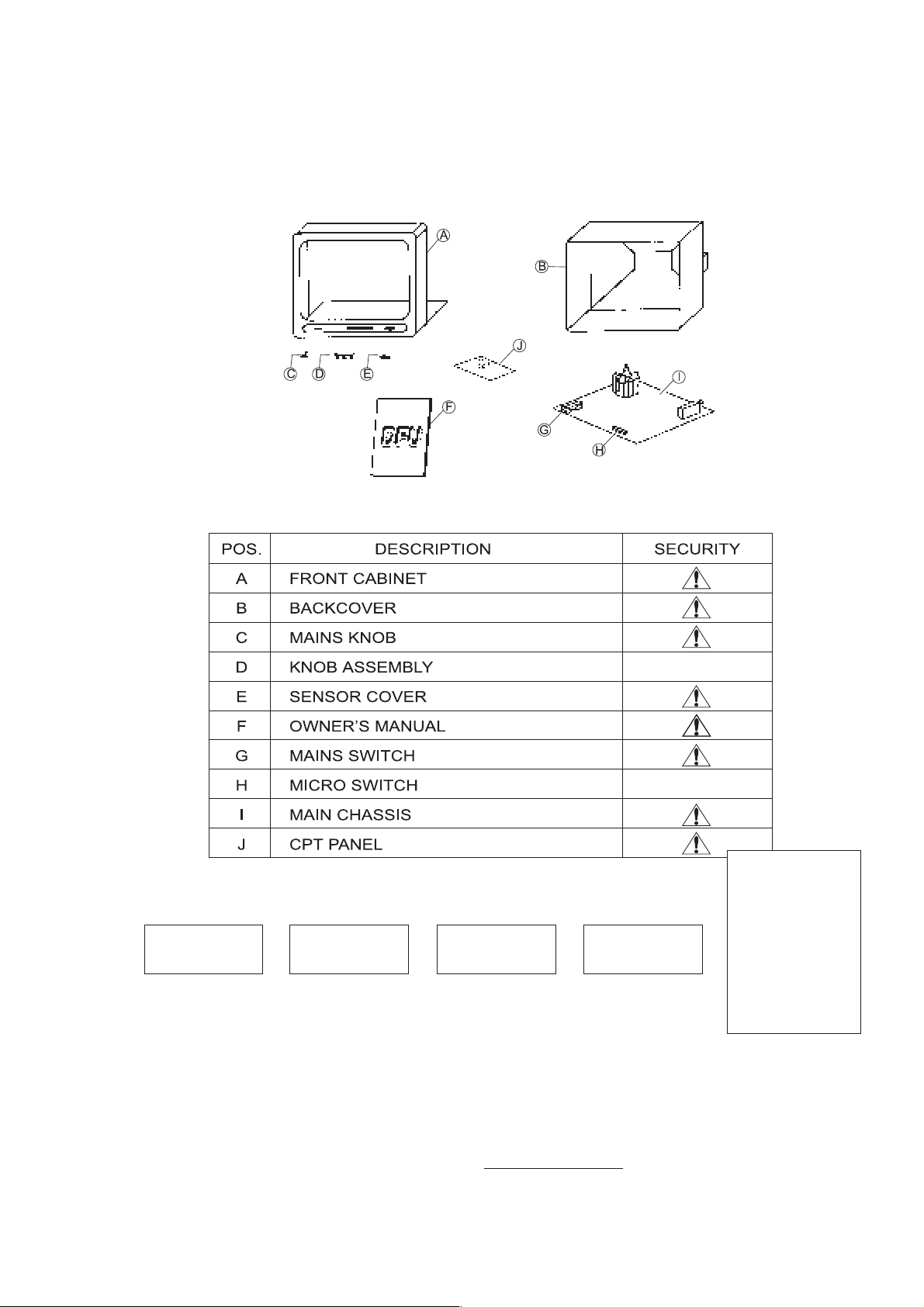
Mechanical Parts List
CTN-BB CHASSIS
**
HOW TO ORDER
EXAMPLE: FRONT CABINET OF TV700TX COLOUR BLUE:
TV MODELSCREENPOSITION
COLOUR
*
A * 14 * TV700TX * AZ
17
NG-BLACK
BL-WHITE
GR-GREY
MA-IVORY
GO-DARK GREY
VE-GREEN
RS-PINK
RJ-RED
AZ-BLUE
PL-SILVER
Page 18
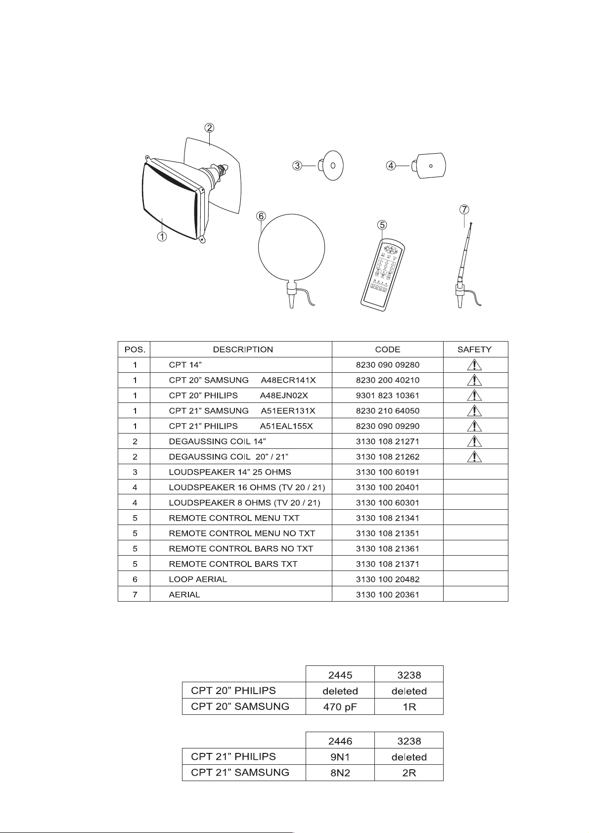
Mechanical and electrical parts list
CTN-BB CHASSIS
Philips CPT 20”/21” can be replace by Samsung CPT 20”/21” or vice versa, modifying components (supplied together
with CPT a Kit) according the following table.
18
Page 19

3130 105 2423.1
 Loading...