

Page 1

23WL46G 30WL46G
L6B TFT- LCD TV
SERVICE MANUAL
Page 2

CONTENTS
PAGES
Safety instructions
Technical specifications
Panel Specification
Back appearance of TV
Interconnectıon Diagram
Block diagram
Block diagram of power supply
Service mode
Service Mode items and values
Data sheet of important IC’s and parts
1
2
3
5
5
6
7
8
10
11
Recommended Part List
Frequency list of channels
23
25
Page 3
SAFETY PRECAUTIONS
GENERAL GUIDELINES
1. It is advised to insert an isolation transformer in the
AC supply before servicing a hot chassis.
2. Always use the manufacturer’s replacement safety
components. The critical safety components marked
with on the schematics diagrams should not be
by other substitutes. Other substitute may create the
electrical shock , fire or other hazards. Take
attention to replace the spacers with the originals.
Furthermore where a short circuit has occurred ,
replace those components that indicate evidence of
overheating.
3. After servicing , see that all the protective devices
such as insulation barriers, insulation papers, shields
and isolation R-C combinations are correctly
installed.
4. When the receiver is not being used for a long time
of period of time , unplug the power cord of the
Adaptor from the AC outlet.
Color TFT LCD Module is very sensitive
both electrically and physically.Users,
therefore, are requested to follow the
“Guidance of handling color TFT LCD
Module”on the followings.
1 -
Be careful not to make scratch on the
polarizer.
Surface of polarizer is soft and can be physically
damaged easily.Please do not touch, push or rub
polarizer surface with materials over HB hardness.
2 - Keep clean the surface.
Please wear rubber glove when touch the surface of
LCD screen. Please use soft and anti-static material
as cleaner.
3 -Keep out of water.Water on/in the LCD may
cause electrical short or corrosion. Please wipe out
dry or water carefully
4 -Prevent swift Temperature & Humidity
change.Instantaneous temperature and/or humidity
change can make dew or ice which cause
nonconformance such as malfunction.
5 - High temperature & high
reduce the life-time.
LCD is not proper to be used at high temperature
and high humidity. Please keep specified
temperature and humidity condition.
6 - Keep out of Corrosive Gas.Corrosive gas
effect the polarizer and the circuit chemically and
cause defects accordingly.
.
humidity
There are electro-static sensitive components such
as CMOS in LCD Module. Please earth human
body when handle the LCD.In addition, please do
not touch the interface connector pin with bare.
8 - Do not operate for a long time under
the same pattern
Operating LCD for a long time under the same
pattern can cause image persistence and can
damage it. Please follow following guidance.
1. Turn the power off when do not use.
2. Change the pattern periodically.
LEAKAGE CURRENT COLD CHECK
1.
Unplug the AC cord and connect a jumper
between the two prongs of the plug.
2. Turn the receiver’s power switch.
3. Measure the resistance value with an ohmmeter,
between the jumpered AC plug and each exposed
metallic cabinet part on the receiver. When the exposed
metallic part a return path to the chassis the reading
should be between 4Mohm and the 20Mohm. When the
exposed metal does not have a return path to the chassis,
the reading must be infinite.
LEAKAGE CURRENT HOT CHECK
1.
Plug the AC cord directly in to the AC outlet. Do
not use an isolation transformer for this check.
2. Connect a 2Kohm 10W resistor in series with an
exposed metallic part on the receiver and an earth,
such as a water pipe.
3. Use an AC voltmeter with high impedance to
measure the potential across the resistor.
4. Check each exposed metallic part and check the
voltage at the each point.
5. Reverse the AC plug at the outlet and repeat each of
the above measurements.
6. The potential at the any point should not exceed 1.4
Vrms. In case a measurement is outside the limits
specified , there is the possibility of a shock hazard ,
and the receiver should be repaired and rechecked
before it is returned to the customer.
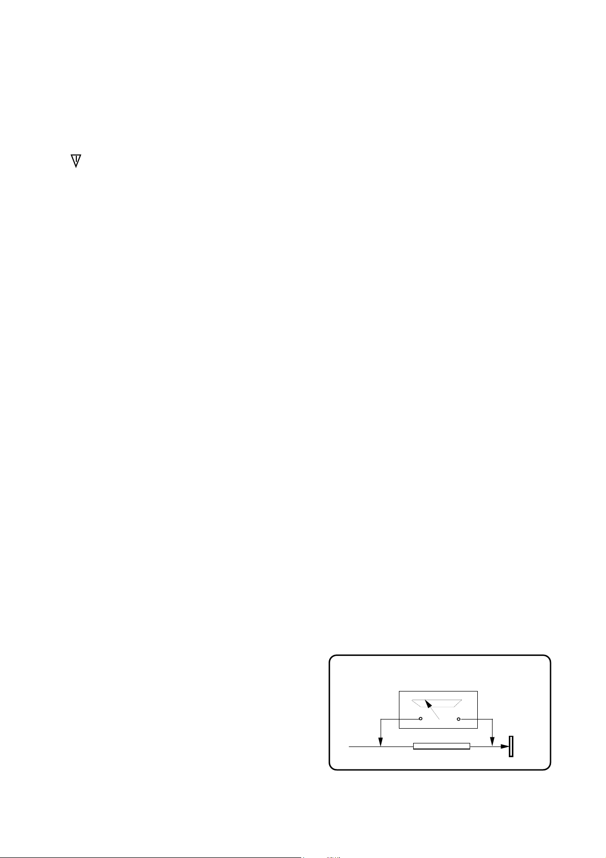
HOT CHECK CIRCUIT
TO INSTRUMENTS
EXPOSED
METALLIC PARTS
AC-Voltmeter
Water pipe
(earth)
2 K Ohm
7 - Electrostatic discharge can make
Damage
Page 4
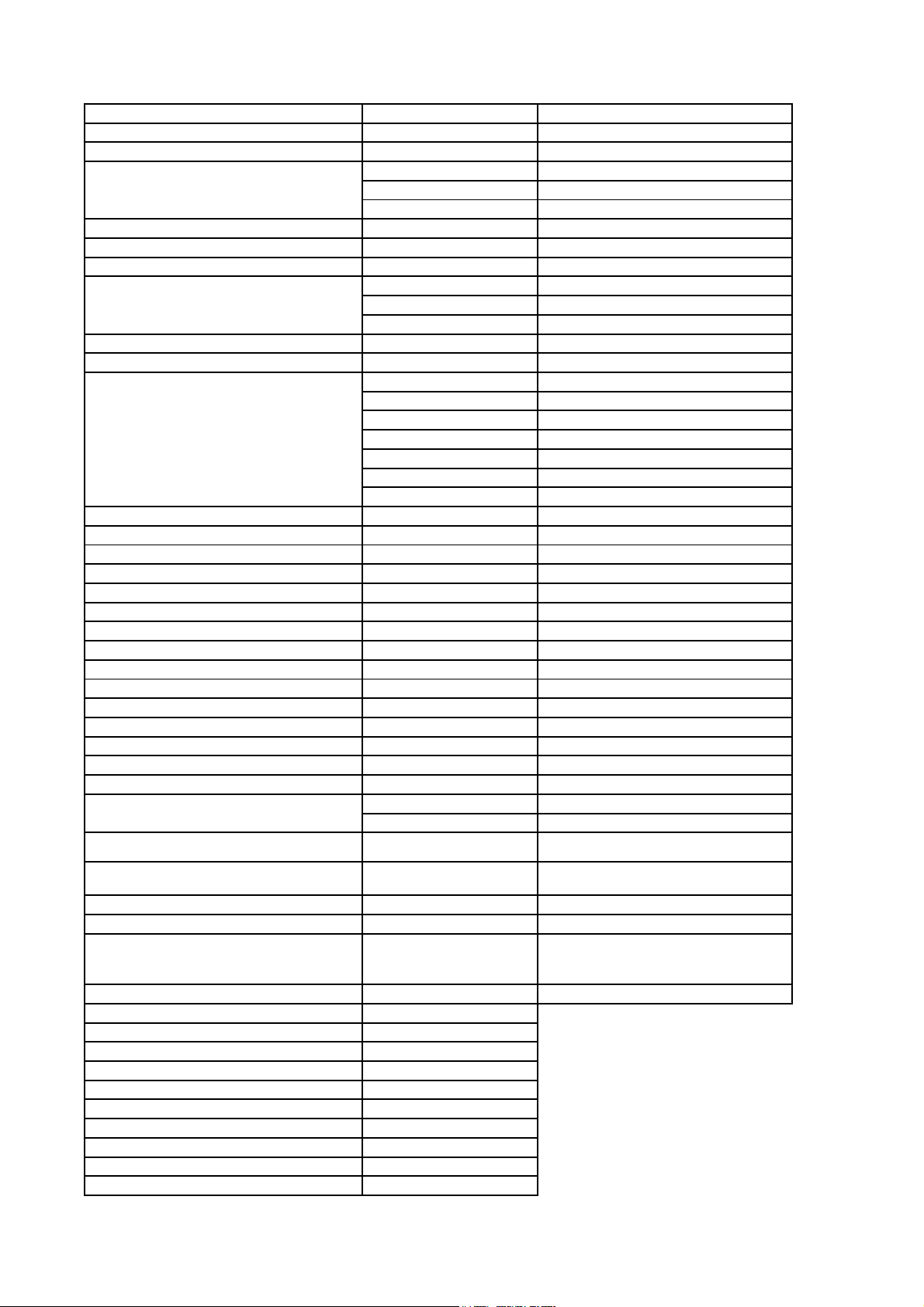
L6B TECHNICAL SPECIFICATION
Receiving System PAL B/G+I+D/K SECAM L/L'
Comb Filter Adaptive 4H\2H
LTI, CTI Filters +
DVI 1.0 Compliant +
DVI Receiver
Gamma Correction 8 to 10-bit LUT
PIP\PAP\POP\PAT +
OSD Graphics Based 8-bit\pixel
Teletext
WSS +
VPS\PDC +
Picture Formats
(4:3, 16:9, 14:9, Panorama, LetterBox,
Subtitle)
WSS (Wide Screen Signalling) +
ATS (Automatic Tuning System) Frequency Search
Manual Search Channel Table Search
Number of Program Storage +
No Ident Timer +
Picture Freeze +
Equalizer +
AVL (Automatic Volume Level) +
Sound Status Memory +
Picture Status Memory +
Swap +
Child Lock +
Program Lock +
Picture Format Switching Tru Pin 8 +
Auto RGB Detect Tru Pin 16 +
Timer
Picture Smart (User, Soft, Natural, Rich) +
Sound Smart (User, Music, Sports, Cinema,
Speech)
Scart2 Out Selectable +
S-Video Input Through Scart2 +
Audio Output Power
RMS in Max at 10% THD)
Stereo (German A2, Nicam, BTSC) German A2, Nicam
S-video In (DIN) 1
AV In (3 RCA) 1
AV Out (3 RCA) 1
PC Audio (L, R) 1
D-Sub 15 1
Headphone 1
CVBS In 4
Y\C In 1
DVI In YES
CVBS Out 4
Resolution VGA to SXGA
2 Pixel \ Clk Support +
Level (1.5, 2.5, Teleweb) Teletext 1.5
Type (Fast\Top\Simple) Simple, Fast, Top
Page Memory 800p
4:3 +
16:9 +
14:9 +
Panorama +
Letterbox +
Subtitle +
Zoom +
Off Timer (Sleep Timer) +
On Timer +
+
2x5W for 22"W, 23"W
2x10W for 26"W
2x10W for 30"W
Page 5
-
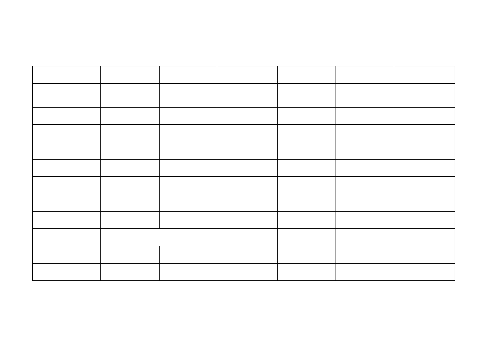
PANEL SPECIFICATION
Sizes 22" 23" 26" 27" 30" 32"
Manufacturer Samsung
Interface
Resolution
Brightness (cd/m2)>=
Contrast>=
Response Time
(Tr+Tf) msec =<
Viewing Angle
R\L\H\L>=
Adaptor İnput
PoweR consumptions
St-By Power
Consumption
Single LVDS Single LVDS Singlel LVDS Singel LVDS Single LVDS Single LVDS
WXGA (1280x720) WXGA (1280x768) WXGA (1280x768) WXGA (1280x720) WXGA (1280x768) WXGA (1280x768)
85/85 85/85 85/85 85/85 85/85/85/85 85/85/85/85 85/85/85/85 85/85/85/85
100W 100W 120W 120W 140W 180W
Samsung LG
Philips Hannstar
450 450 450 550 550 450
500 400 400 600 600 700
25 25 25 25 25 23
15V 24V Built-in TV Built-in TV Built-in TV Built-in TV
<4W <4W <4W <4W <4W <4W
Samsung LGPhilips AUO
Chimei
Chimei AUO
LG-Philips
Input Range
100V-240V/50- 60Hz 100V-240V/50- 60Hz 100V-240V/50- 60Hz 100V-240V/50- 60Hz 100V-240V/50- 60Hz 100V-240V/50- 60Hz
Page 6
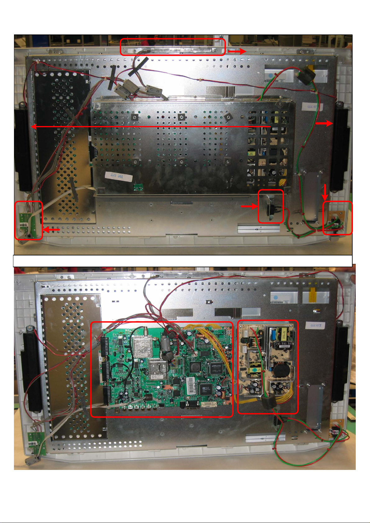
BACK SIDE APPEARANCES
CONTROL
BOARD
SPEAKERS
POWER
SWITCH
LED/IR BOARD
MAIN
CHASSIS
220VAC INPUT
POWER SUPPLY
BOARD
NOTE: LOCATION AND THE SHAPE OF IR /LED BAORD, CONTROL BOARD AND MAIN SWITCH
BOARD MAY CHANGE ACCORDING TO THE COSMETIC OF THE TV AND SIZE
Page 7
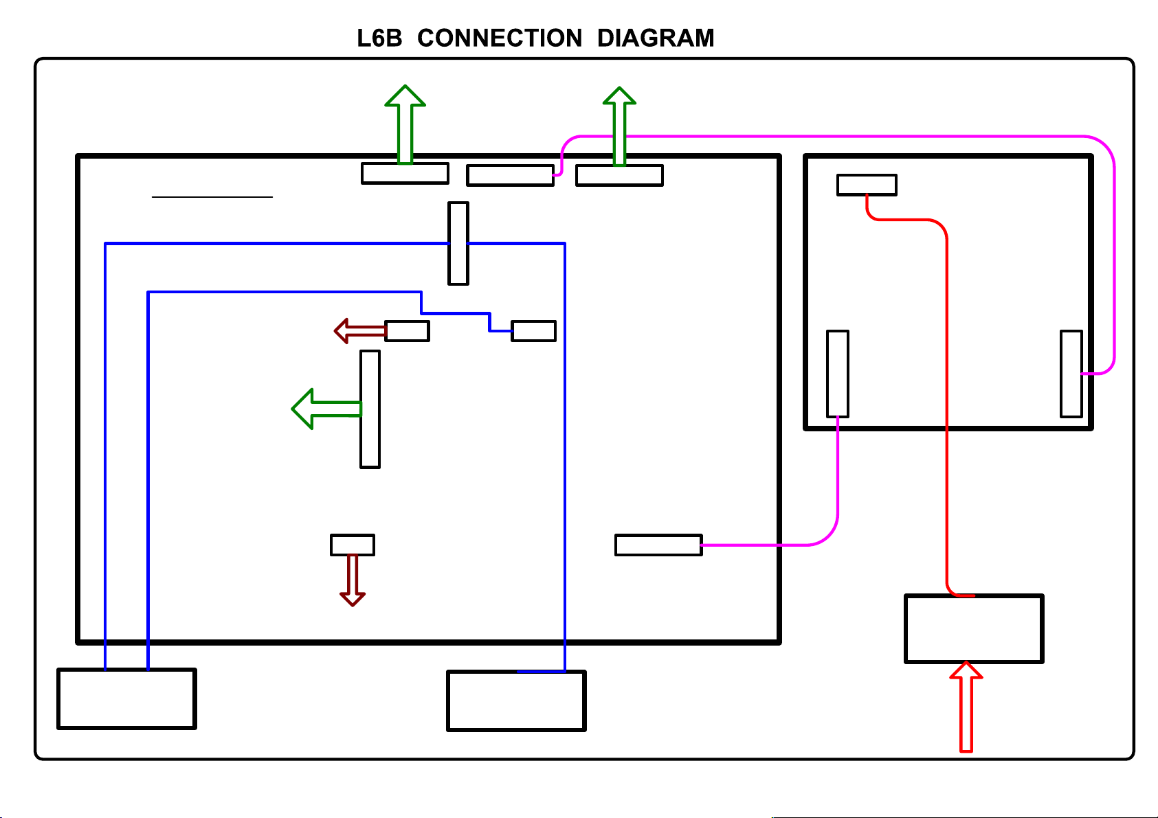
TO PANEL
MAIN CHASSIS
SPEAKER
PANEL
TO
S50
S150
S2
S350
JP451JP452
S550
JP453
JP450
CN1
POWER
SUPPLY
MODULE
CN2CN3
IR RECEIVER/LED
MODULE
TO HEADPHONE JACK
KEY BOARD
MODULE
MAIN POWER
SWITCH
MODULE
220V AC
INPUT
Page 8
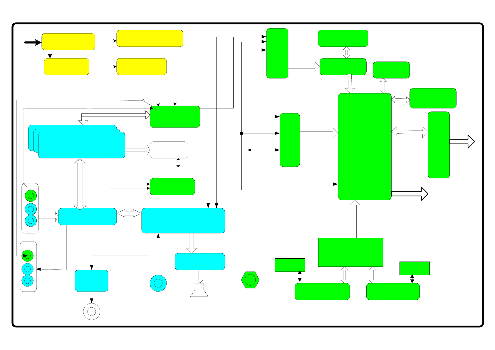
L6B BLOCK DIAGRAM
RF In
AV-Out Video
AV4 Video-In
AV4
Audio-In
Tuner-Main
Tuner-PIP
SCART 1 2 3
Audio-In/Out
Audio-Switch
TDA6420
IF IC TDA9886T
IF IC TDA9886T
Video In/Out
I2C Communication
SC1-SC2 RGB
Audio
In-Out
PIP-Video
Main-Video
Video Switch
TDA6415C
Pin 8 Switch
PCF8591
RGB Switch
PI5V30
AUDIO PROCESSOR
MSP3410D
QSS-Main
QSS-PIP
Video-Main
Video-PIP
Scart RGB
Multi Standard
Video Decoder
SAA7118MP
Multi Standard
Video Decoder
16 Bit
YUV
SAA7118MP
MT48LC16M
De-Interlacer
24 Bit RGB
16 Bit
YUV
IR In
SDRAM
PW1231
PROCESSOR
De-Interlacer
Micro-Cont.
Gamma Corr.
EEPROM
24C64
PW181
IMAGE
Scaler
OSD
48 Bit RGB VS/HS
Flash Memory
AM29VL160
Progressive
or Intrelaced
24 Bit Dual
RGB ,HS,VS
DE,PCLK
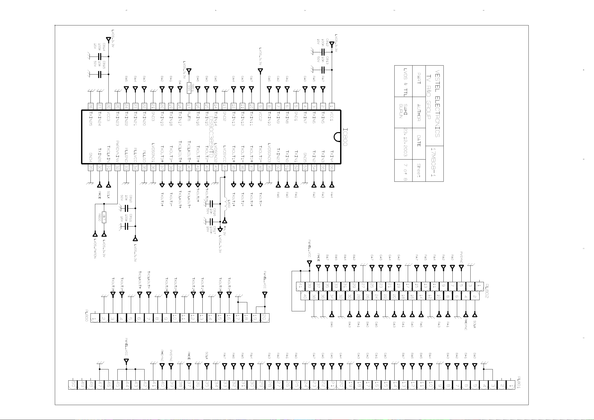
DS090C385
LVDS Transmitter
Stand by
LED’s
Reset
Mute
B/L Enable
Digital Dim
TO THE
PANEL
AV Out Audio
Headphone Jack
Headphone
Amp.
TDA1308
PC DVI Audio -In
Audio Amplifier
TA2024
Speaker
SVHS Y/C
SVHS Socket
EEPROM
24LC21
Dual İnterface for
RGB HS/VS-In
D-SUB 15 socket
FPD
AD9887
EEPROM
24LC21
DVI Input
DVI Socket
Page 9
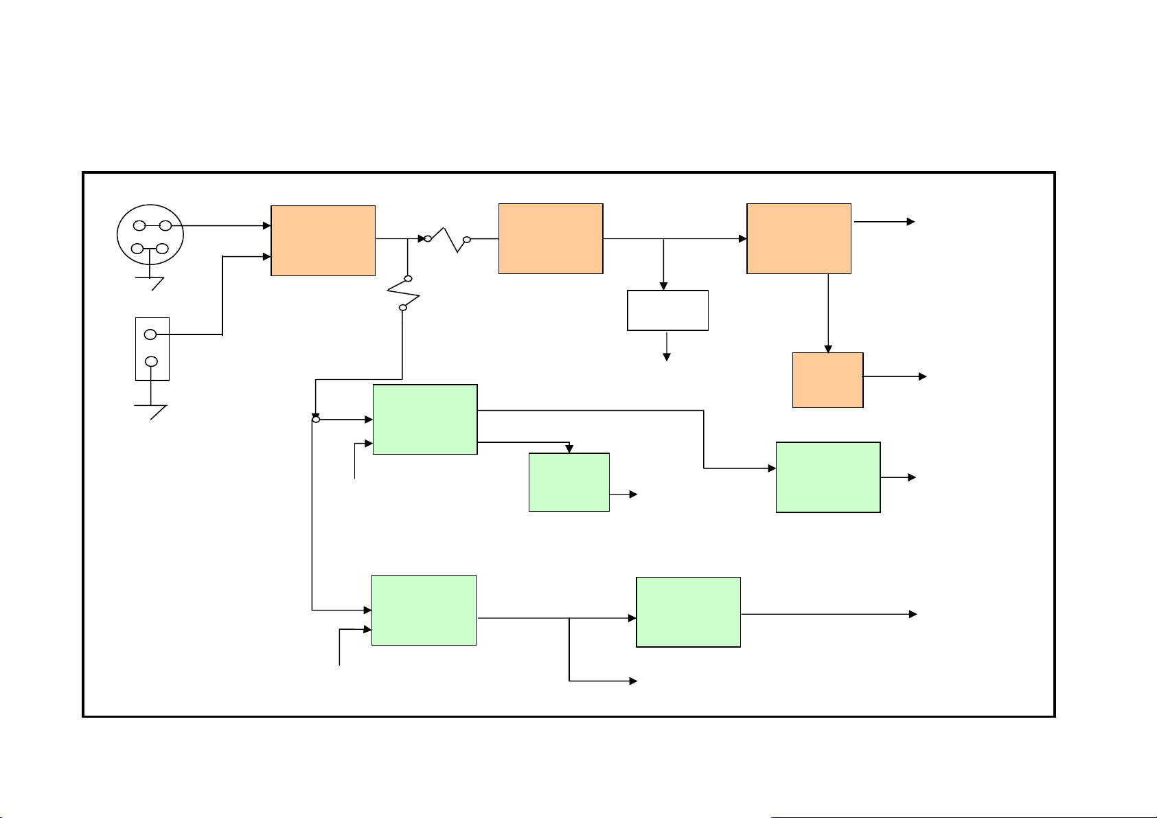
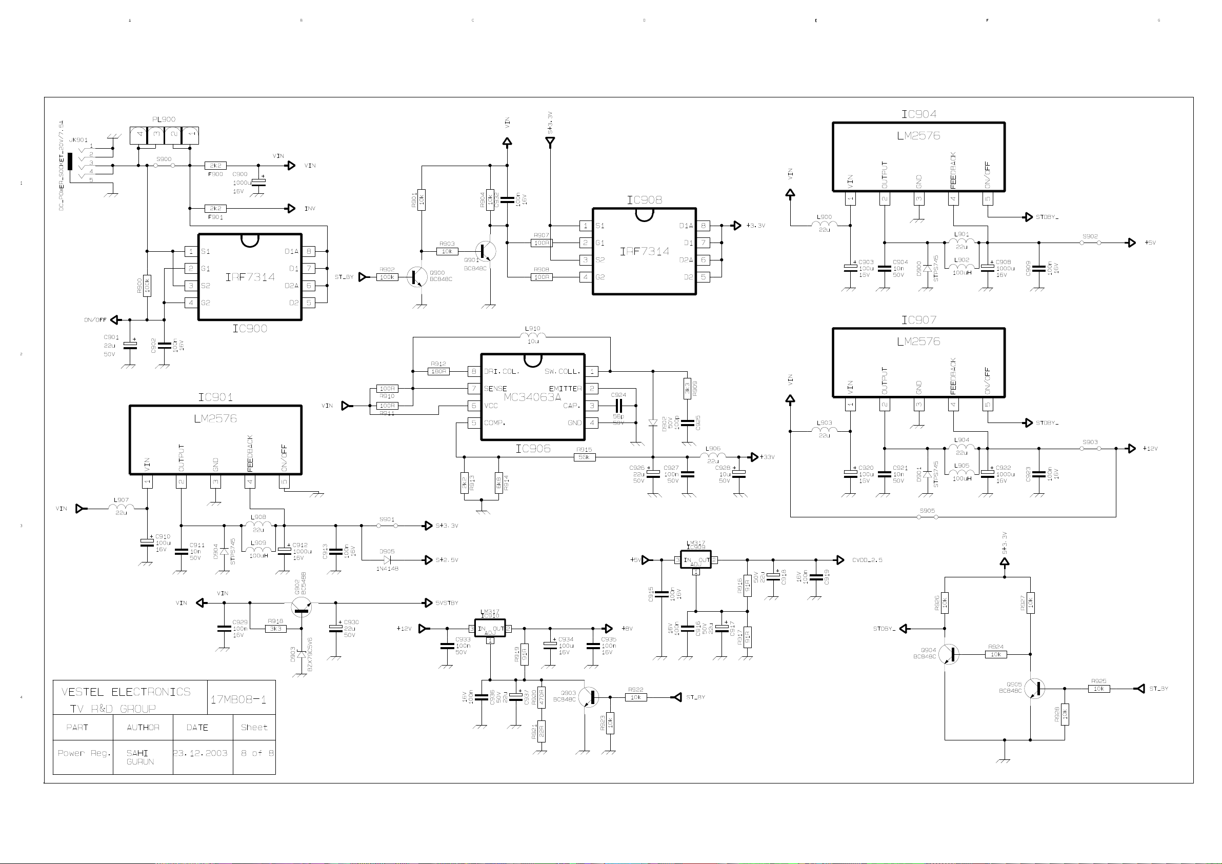
L6B POWER SUPPLY BLOCK DIAGRAM (MAIN CHASSIS)
J450
12V F450 +2,5V_STBY
U451
FDS9933A
DC_IN
GND
S450 +3,3V_STBY
(5V) +5V_STBY
F451
U454
LM2576
VOLTAGE
DOUBLER
U458
NCP1117
GND
12V '33V +1,5V_STBY
U452
FDS9933N
STAND_BY +3,3V
U453
FDS9933N
PNL_EN +12V_INVERTER
12V_AMP
+5V
U457
NCP1117
+12V PANEL_POWER
U455
LM2576
U450
NCP117
U456
LM317
+8V
Page 10

L6B SERVICE MENU
1. Activating the Service Menu
When the menu is on the screen press ‘9’, ‘3’, ’0’, ’1’ on the remote controller. This will
activate the service menu.
2. Service Menu Structure
The service menu has three items: display, calibre and version
2.1 Display
Display item has seven options:
a- Panel
Panel option gives information about the current panel resolution. It is a read only
option and can not be set.
b- Power on time
Power on time gives information about the last update time of the SW running. It
is a read only option and can not be set.
c- Backlight on time
Backlight on time option reserved.
d- Scart prescale
Scart prescale option sets the prescale values for the input sounds entering the scart
input of the MSP(Micronas Sound Processor). Changing this value you can adjust
the level of the output sound going to loudspeakers for all the sources except the
Tuners. The range is between 0 and 100.
e- nicam prescale
Nicam prescale option sets the prescale values for the Nicam standard sounds for
tuner inputs. Changing this value you can adjust the level of the output sound
going to loudspeakers for Nicam sounds entering the analog sound input of MSP.
The range is between 0 and 100.
f- fm/am prescale
fm/am prescale option sets the prescale values for the FM/AM standard sounds for
tuner inputs. Changing this value you can adjust the level of the output sound
going to loudspeakers for FM/AM sounds entering the analog sound input of MSP.
The range is between 0 and 100.
g- Agc(Automatic Gain Control) adjust
Agc adjust option sets the input voltage going to IF decoder AGC pin. Changing
this value you can adjust this voltage for optimum Tuner performance. The range
is between 0 and 31.
h- R/G/B Brightness/Contrast: These are used for color bias adjustment. The range is
Between 0 and 255
Page 11

2.2 Calibre
2.3 Version
Calibre item has nine options:
a- video format
Video format option force the video format to the desired format. Selectable
formats are Auto, Pal, NTSC and SECAM.
b- colorspace
Colorspace option gives the information about the video input colorspace input to
PW181 IC. Do not change this value unless an error occurred in the colors
displayed.
c- test pattern
This option activates the internal pattern of PW181 IC. There are 3 choices: none,
vert bars, solid color. None will deactivate the internal pattern. Vert bars choice
activates the bar pattern for the selected color component. Solid color activates the
solid pattern with one color selected in color component and also you can change
the level of the color by solid field level.
d- Color components:
This option selects the color for the internal pattern of PW181 IC. There are 4
choices: all, red, green and blue. If you choose all, you can see the white pattern
and if you choose one of the other choices you can see the test pattern with the
selected color.
e- solid field level
This option will adjust the level of the colors for the test pattern. The range is
betwwen 1 and 64.
f- Initial ATS
This option will enable or disable the Initial setup for the TV. Setting this option to
On, the TV will open from the Quick setup menu. Setting this option to Off will
disable this option.
g- factory reset
Factory reset option executes a reset operation for the NVRAM. Pressing OK
when this option is selected will erase the NVRAM and load default values to
NVRAM.
h- dpms
This option selects the Power option for the TV. Setting this option to On the TV
will switch to the last state for power on transition. Setting this to Off will disable
this option and the TV will always switch to Stand-by state while power on
transition.
i- osd timeout
This option sets the OSD timeout for the main menu structure. Selections are 5, 15
and 60 secs. The default is 60 sec.
This item gives the information about the version of the software. Also you can see the
last modified time for the GUI(graphical user interface).
Page 12
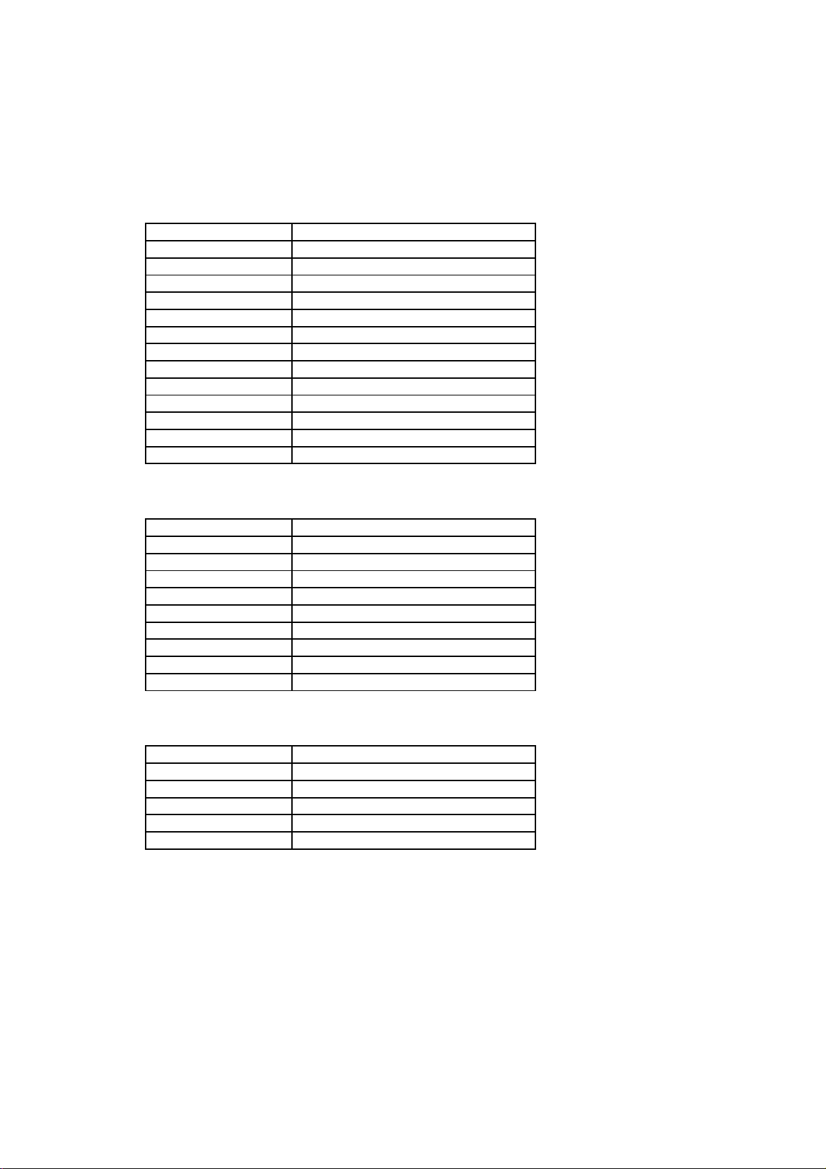
L6 CHASSIS SERVICE MODE ITEMS
display menu
ITEM TYPICAL VALUES/OPTIONS
panel 1280x768
power on time 03:39:45
back light time 03:39:45
scart prescale 25
nicam prescale 45
fm/am prescale 24
agc adjust 16
red brightness 128
red contrast 128
green brightness 128
green contrast 128
blue brightness 128
blue contrast 128
calibre menu
ITEM TYPICAL VALUES/OPTIONS
video format auto
color space RGB
test pattern none
color components all
solid field level 33
initial ats on
factory reset press <ok> to reset
dpms on
osd time out 60 sec
version
ITEM TYPICAL VALUES/OPTIONS
Software
SL630T_CH1_T13 L6B 1.22 Chi30
GUI
Project; L6B Toshiba
Generated Date: October 01,2004 at 22.42
Page 13
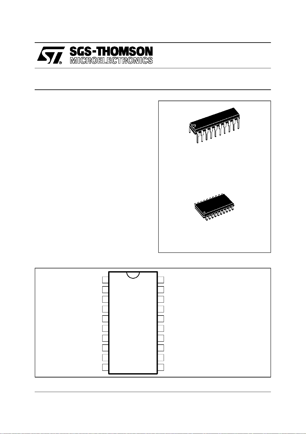
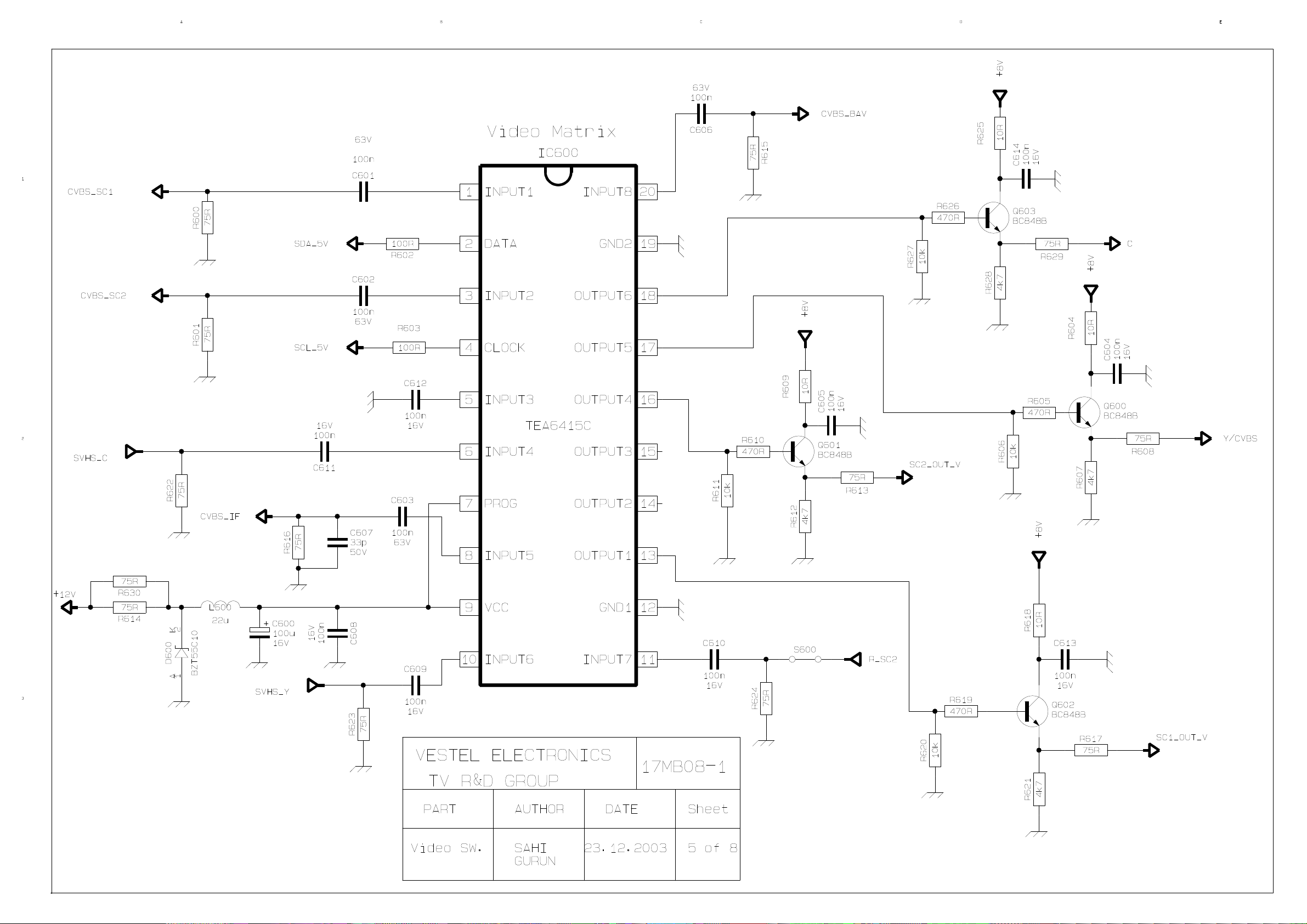
BUS-CONTROLLED VIDEO MATRIX SWITCH
■
20MHz BANDWIDTH
■
CASCADABLE WITH ANOTHER TEA6415C
(INTERNAL ADDRESS CAN BE CHANGED BY
PIN 7 VOLTAGE)
■
8 INPUTS (CVBS, RGB, MAC, CHROMA, ...)
■
6 OUTPUTS
■
POSSIBILITY OF MAC OR CHROMA SIGNAL
FOR EACH INPUT BY SWITCHING-OFF THE
CLAMP WITH AN EXTERNAL RESISTOR
BRIDGE
■
BUS CONTROLLED
■
6.5dB GAIN BETWEEN ANYINPUT AND OUTPUT
■
-55dB CROSSTALKAT5MHz
■
FULLYESD PROTECTED
DESCRIPTION
The main functionof the TEA6415Cis to switch 8
videoinput sources on the 6 outputs.
Each output can be switched to only one of the
inputs whereas but any same input may be connectedto several outputs.
Alltheswitchingpossibilitiesarecontrolledthrough
2
the I
C bus.
TEA6415C
DIP20
(Plastic Package)
ORDER CODE : TEA6415C
SO20
(Plastic Micropackage)
ORDER CODE : TEA6415CD
PINCONNECTIONS
INPUT
DATA
INPUT
CLOCK
INPUT
INPUT
PROG
INPUT
V
CC
INPUT
1
2
3
4
5
6
7
8
9
10
20
19
18
17
16
15
14
13
12
11
INPUT
GROUND
OUTPUT
OUTPUT
OUTPUT
OUTPUT
OUTPUT
OUTPUT
GROUND
INPUT
6415C-01.EPS
Page 14
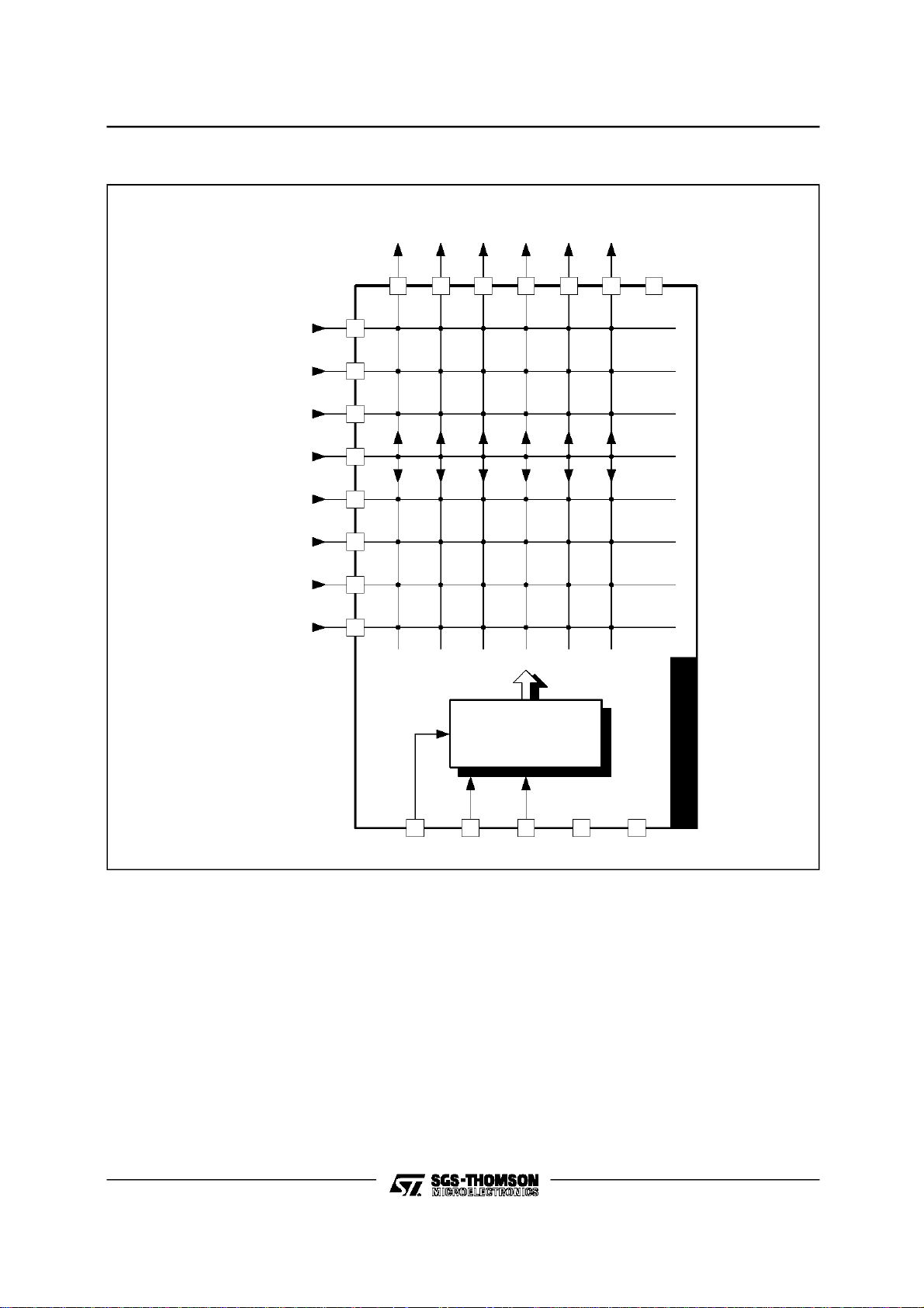
TEA6415C
BLOCK DIAGRAM
CVBS
(MAC/DEC)
CVBS
(PERI PLUG1)
CVBS
(AMTUNER)
MAC S IGNAL
(AMTUNER)
CVBS
(PERI PLUG2)
CVBS
(FM TUNER)
MAC S IGNAL
(FM TUNER)
SYNCHRO
(TTX/BTX)
PERI
TV2
TTX LUMA
CHROMA
POWER
PERI
TV1
18 17 16 15 1 4 13 12
1
3
5
6
8
10
11
20
PIP MAC
DEC.
GND
274
DATA GNDCLOCK V
GENERALDESCRIPTION
ThemainfunctionoftheICistoswitch8videoinput
sources on6 outputs.
Each output can be switched on onlyone of each
input. On each input an alignment of the lowest
level ofthesignal ismade (bottomof synch.top for
CVBS or blacklevel for RGB signals).
Each nominal gain between any input and output
is 6.5dB.For D2MAC or Chroma signalthe alignment is switched off by forcing, with an external
resistor bridge,5 V
ontheinput. Each inputcan
DC
be used asa normal input or as aMAC orChroma
T
E
BUS
DECODER
A
6
4
1
5
C
919
PROG
CC
input (withexternal resistorbridge). All the switching possibilitiesare changedthrough the BUS.
Driving 75Ω load needsan external transistor.
It is possible to have the sameinput connectedto
severaloutputs.
The starting configuration upon power on (power
supply: 0 to10V) isundetermined.
In this case, 6 words of 16 bits are necessary to
determineone configuration.In othercase,1 word
of 16 bits isnecessaryto determineone configuration.
6415C-02.EPS
Page 15
I2C-buscontrolled single and multistandard
alignment-free IF-PLL demodulators
1 FEATURES
• 5 V supply voltage
• Gain controlled wide-band Vision Intermediate
Frequency (VIF) amplifier, AC-coupled
• Multistandard true synchronous demodulation with
active carrier regeneration: very linear demodulation,
good intermodulation figures, reduced harmonics, and
excellent pulse response
• Gated phase detector for L and L-accent standard
• Fully integrated VIF Voltage Controlled Oscillator
(VCO), alignment-free, frequencies switchable for all
negative and positive modulated standards via I
• Digital acquisition help, VIF frequencies of 33.4, 33.9,
38.0, 38.9, 45.75, and 58.75 MHz
• 4 MHz reference frequency input: signal from
Phase-Locked Loop (PLL) tuning system or operating
as crystal oscillator
• VIF Automatic Gain Control (AGC) detector for gain
control, operating as peak sync detector for negative
modulated signals and as a peak white detector for
positive modulated signals
• External AGC setting via pin OP1
• Precise fully digitalAutomatic Frequency Control (AFC)
detector with 4-bit digital-to-analog converter, AFC bits
2
readable via I
• TakeOver Point (TOP) adjustable via I
C-bus
2
C-bus or
alternatively with potentiometer
• Fully integrated sound carrier trap for 4.5, 5.5, 6.0,
and 6.5 MHz, controlled by FM-PLL oscillator
• Sound IF (SIF) input for single reference Quasi Split
Sound (QSS) mode, PLL controlled
2
C-bus
TDA9885; TDA9886
• SIF-AGC for gain controlled SIF amplifier, single
reference QSS mixer able to operate in high
performance single reference QSS mode and in
intercarrier mode, switchable via I
• AM demodulator without extra reference circuit
• Alignment-free selectiveFM-PLL demodulatorwith high
linearity and low noise
• I2C-bus control for all functions
2
C-bus transceiver with pin programmable Module
• I
Address (MAD)
• Four I
2
C-bus addresses via MAD.
2 GENERAL DESCRIPTION
The TDA9885 is an alignment-free multistandard
(PAL and NTSC) vision and sound IF signal PLL
demodulator for negative modulation only and
FM processing.
The TDA9886 is an alignment-free multistandard
(PAL, SECAM andNTSC) vision andsound IF signal PLL
demodulator for positive and negative modulation,
including sound AM and FM processing.
3 APPLICATIONS
• TV, VTR, PC and STB applications.
2
C-bus
4 ORDERING INFORMATION
PACKAGE
TYPE NUMBER
NAME DESCRIPTION VERSION
TDA9885T/V3 SO24 plastic small outline package; 24 leads; body width 7.5 mm SOT137-1
TDA9885TS/V3 SSOP24 plastic shrink small outline package; 24 leads; body width 5.3 mm SOT340-1
TDA9885HN/V3 HVQFN32 plastic, heatsink very thin quad flat package; no leads; 32 terminals;
SOT617-1
body 5 × 5 × 0.85 mm
TDA9886T/V3 SO24 plastic small outline package; 24 leads; body width 7.5 mm SOT137-1
TDA9886TS/V3 SSOP24 plastic shrink small outline package; 24 leads; body width 5.3 mm SOT340-1
Page 16
This text is here in white to force landscape pages to be rotated correctly when browsing through the pdf in the Acrobat reader.This text is here in
_white to force landscape pages to be rotated correctly when browsing through the pdf in the Acrobat reader.This text is here inThis text is here in
white toforce landscape pages tobe rotated correctly whenbrowsing through the pdfin the Acrobat reader.white to force landscapepages to be ...
handbook, full pagewidth
external reference signal
or 4 MHz crystal
7 (5)
DGND
REF AFC
AFC DETECTOR
SOUND TRAPS
FM-PLL DEMODULATOR
12 (11)18 (20)20 (22)
SIOMADSDASCL
4.5 to 6.5 MHz
AUDIO PROCESSING
AND SWITCHES
NARROW-BAND
(18) 17
CVBS
video output: 2 V (p-p)
[1.1 V (p-p) without trap]
AUD
(7) 8
(3) 5
(4) 6
4 (2)10 (9)
MHC108
DEEM
AFD
audio output
de-emphasis
network
C
AF
VIF2
VIF1
SIF2
SIF1
2 (31)
1 (30)
24 (27)
23 (26)
TOP
TUNER AGC
SUPPLY
V
P
C
VAGC(pos)
TAGC
14 (15)
C
AGC(neg)
VAGC
VIF-AGC
SINGLE REFERENCE QSS MIXER
SIF AGC
(6, 12, 13, 14, 17,
19, 25, 28, 29, 32)
13
n.c.AGND
VIF-PLL
filter
(1)
C
BL
INTERCARRIER MIXER
AND AM DEMODULATOR
C
AGC
VPLL
19 (21)9 (8) 16 15 (16) 21 (23)
RC VCO
VIF-PLL
OUTPUT
PORTS
22 (24)3 (1)
OP1 OP2 FMPLL
DIGITAL VCO CONTROL
TDA9885
TDA9886
MAD
I2C-BUS TRANSCEIVER
11 (10)
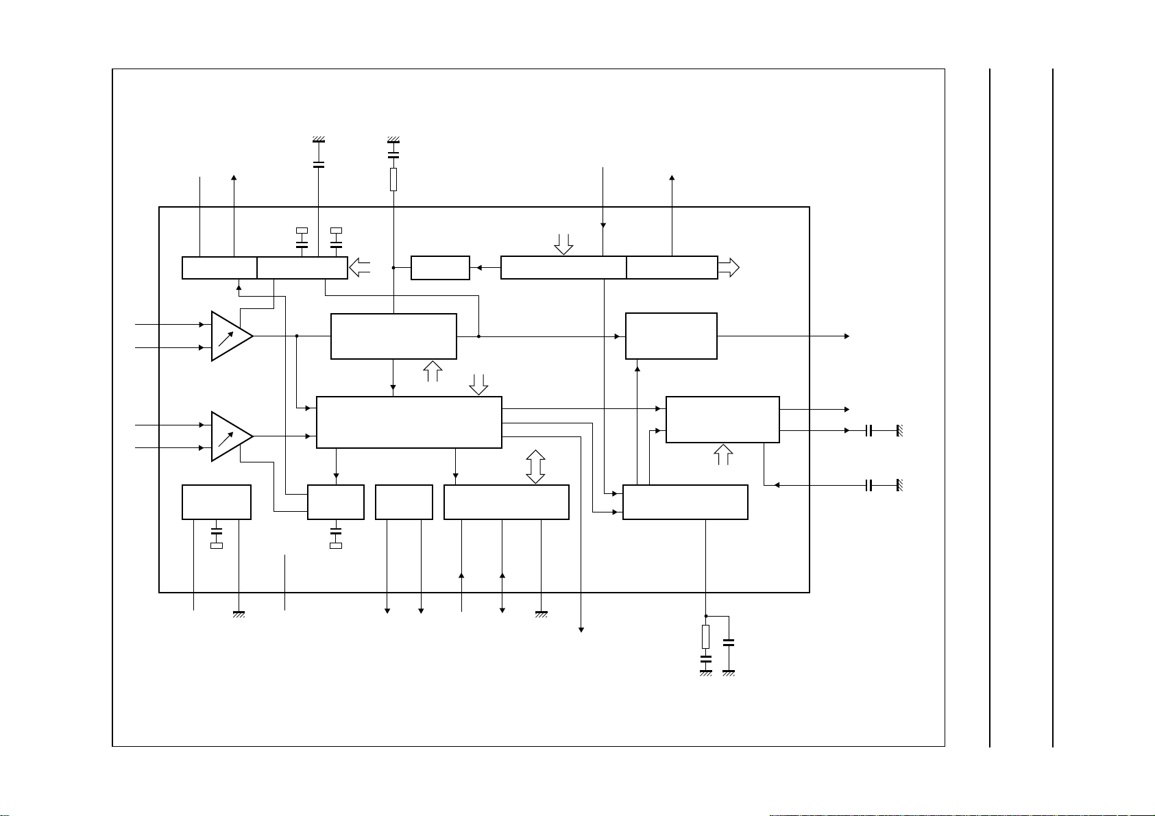
6 BLOCK DIAGRAM
alignment-free IF-PLL demodulators
I
2
C-buscontrolled single andmultistandard
TDA9885; TDA9886
(1) Not connected for TDA9885.
Pin numbers for TDA9885HN in parenthesis.
sound intercarrier output
and MAD select
Fig.1 Block diagram.
FM-PLL
filter
Page 17
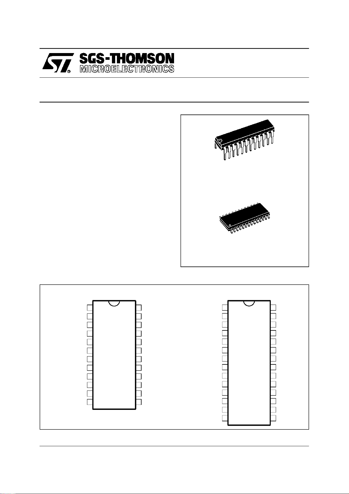
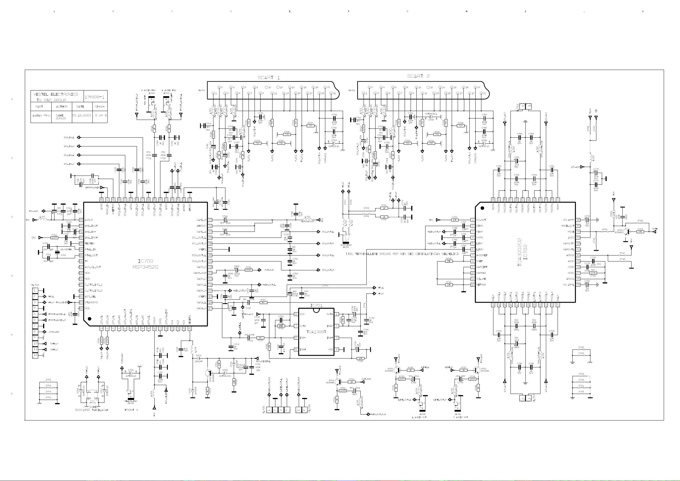
BUS-CONTROLLEDAUDIO MATRIX
.
5 STEREOINPUTS
.
4 STEREOOUPUTS
.
GAIN CONTROL 0/2/4/6dB/MUTEFOR EACH
OUTPUT
.
CASCADABLE(2 different addresses)
.
SERIALBUS CONTROLLED
.
VERYLOW NOISE
.
VERYLOW DISTORSION
DESCRIPTION
The TEA6420 switches 5 stereo audio inputs on
4 stereo outputs.
All theswitching possibilitiesare changed through
2
C bus.
the I
TEA6420
SHRINK24
(Plastic Package)
ORDER CODE : TEA6420
SO28
(Plastic Micropackage)
ORDER CODE : TEA6420D
PINCONNECTIONS
GND
CAPACITANCE
V
S
L1
L2
L3
L4
L5
LOUT1
ROUT1
LOUT2
ROUT2
SHRINK24
1
2
3
4
5
6
7
8
9
10
11
12
24
23
22
21
20
19
18
17
16
15
14
13
SDA
SCL
ADDR
R1
R2
R3
R4
R5
ROUT4
LOUT4
ROUT3
LOUT3
GND
CAPACITANCE
V
L1
L2
L3
NC
NC
L4
L5
LOUT1
ROUT1
LOUT2
ROUT2
SO28
1
2
3
S
4
5
6
7
8
9
10
11
12
13
14
28
27
26
25
24
23
22
21
20
19
18
17
16
15
SDA
SCL
ADDR
R1
R2
R3
NC
NC
R4
R5
ROUT4
LOUT4
ROUT3
LOUT3
6420-01.EPS / 6420-02.EPS
Page 18
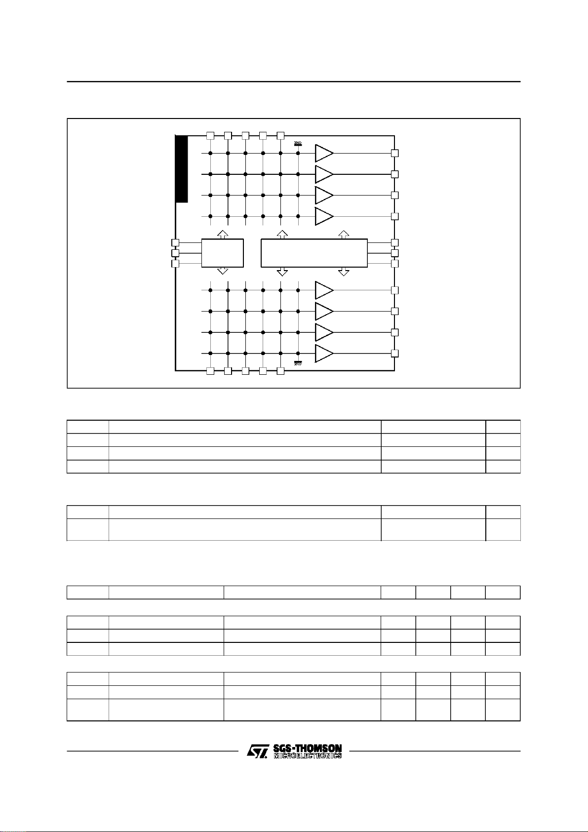
TEA6420
BLOCK DIAGRAM
RIGHT INPUTS
GND
T
E
A
6
4
2
0
V
S
C
SUPPLY BUS DECODER
LEFT INPUTS
GAIN = 0/2/4/6 dB
GAIN = 0/2/4/6 dB
RIGHT
OUTP UTS
SDA
SCL
ADDR
LEFT
OUTP UTS
ABSOLUTEMAXIMUM RATINGS
Symbol Parameter Value Unit
V
T
oper
T
Supply Voltage 10.2 V
CC
Operating Ambient Temperature 0, + 70
Storage Temperature - 20, + 150
stg
6420-03.EPS
o
C
o
C
6420-01.TBL
THERMALDATA
Symbol Parameter Value Unit
R
th(j-a)
Junction Ambient ThermalResistance SHRINK24
SO28
75
75
ELECTRICAL CHARACTERISTICS
=25oC, VS= 10V,RL=10kΩ,RG= 600Ω, f = 1kHz (unlessotherwise specified)
T
A
Symbol Parameter Test Conditions Min. Typ. Max. Unit
SUPPLY
V
I
SVR Ripple Rejection V
MATRIX
V
R
C
Supply Voltage 8 9 10.2 V
S
Supply Current 5 8 mA
S
= 500mV
IN
Input DC Level 4.5 5 5.5 V
IN
Input Resistance 30 50 100 kΩ
I
Channel Separation VIN=2V
S
f = 1kHz Gain = 6dB
RMS
, BW = 20 - 20kHz 70 80 dB
RMS
Gain = 0dB
80
70
90
82
o
C/W
dB
dB
6420-02.TBL
6420-03.TBL
Page 19
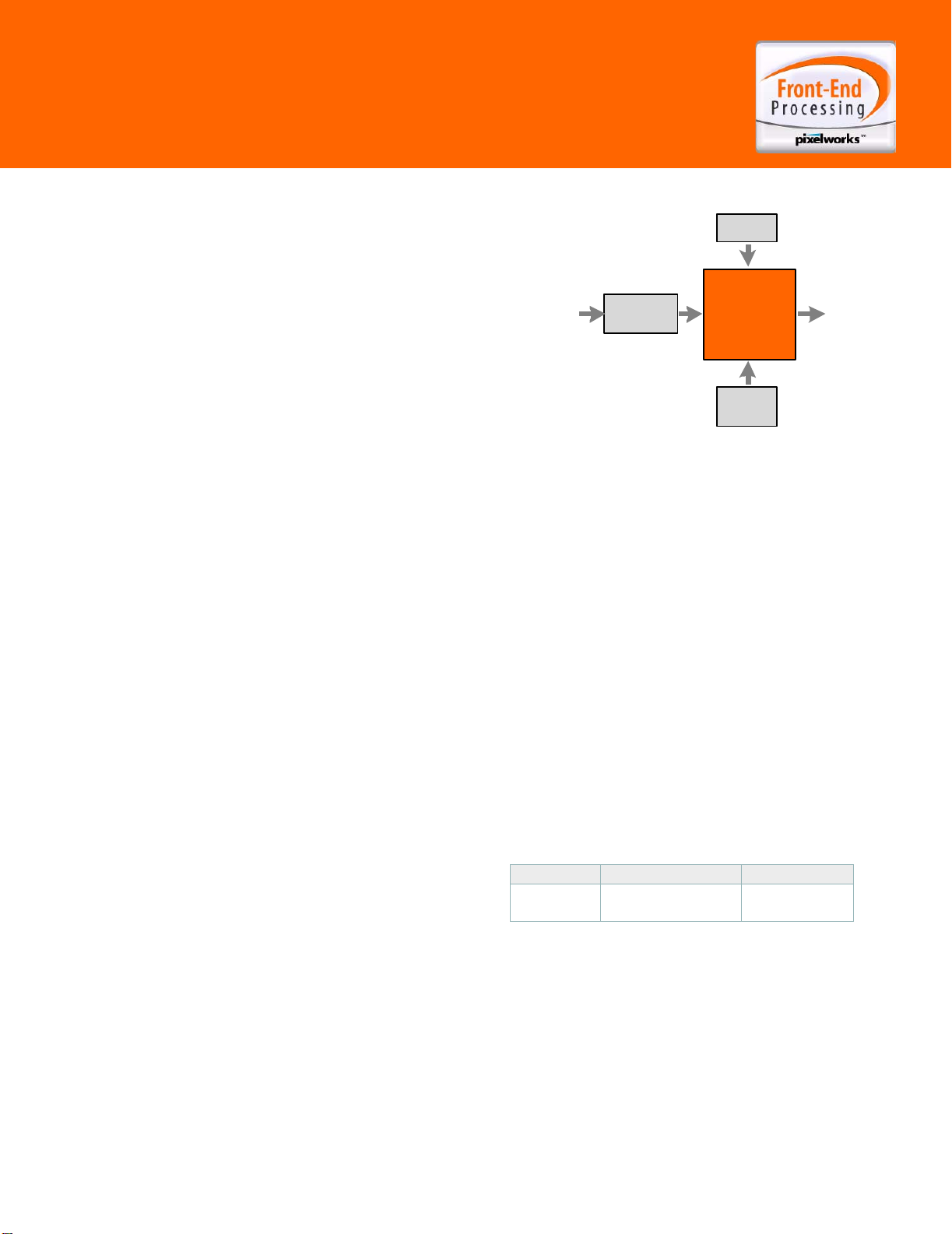
PW1231
Product Specification
General
The PW1231 is a high-quality, digital video signal
processor that incorporates Pixelworks’ patented
deinterlacing, scaling, and video enhancement
algorithms. The PW1231 accepts industry-standard video
formats and resolutions, and converts the input into any
desired output format.The video algorithms are highly
efficient, providing excellent quality video.
The PW1231 Video SignalProcessor combines many
functions into a single device, including memory
controller, auto-configuration, and others. This high level
of integration enables simple, flexible, cost-effective
solutions featuring fewer required components.
Cr ystal
Video
PW1231
System Block Diagram
Video
Decoder
PW1231
SDRAM
Dig i ta l
Output
Features
• Built-In Memory Controller
• Motion-Adaptive Deinterlace Processor
• Intelligent Edge Deinterlacing
• Digital Color/Luminance Transient Improvement (DCTI/DLTI)
• Interlaced Video Input Options, including NTSC and PAL
• Independent horizontal and vertical scaling
• Copy Protection
• Two-Wire Serial Interface
Applications:
For use with Digital Displays
• Flat-Panel (LCD, DLP) TVs
• Rear Projection TVs
• Plasma Displays
• LCD Multimedia Monitors
• Multimedia Projectors
Device Application Package
PW1231
PW1231-L
NOTE: “L” denotes lead (Pb) free
Up to XGA 160-pin PQF
Page 20
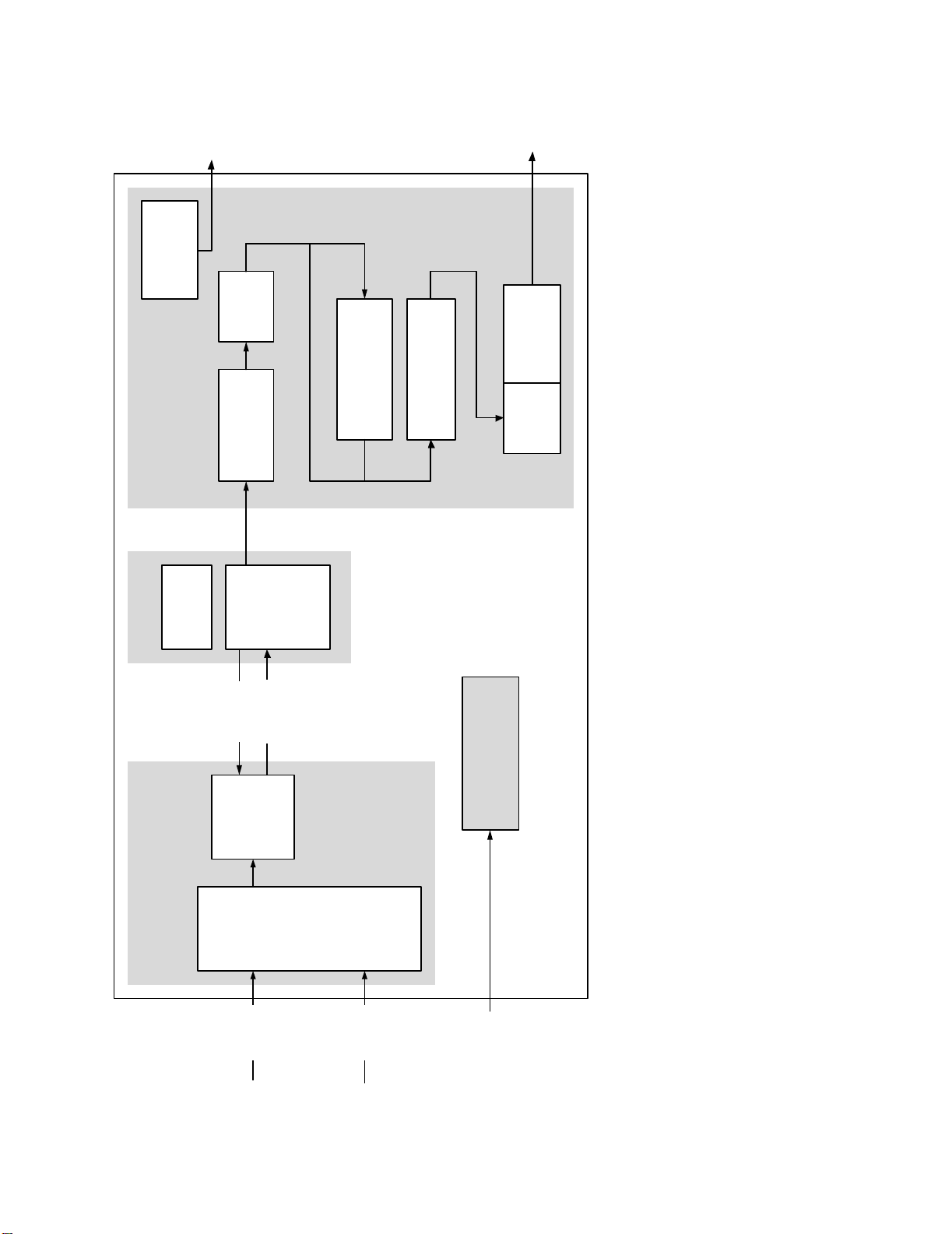
Data
Digital
Output
Ti m in g
Timing
Dis pla y
YU V
Digital
Output
Up
Scaler
HSync
Ti mi ng
VSync /
Video
Enhancem ents
Deinterlace r
RGB
Color Space
Converter (CSC)
Blue
Screen
Dis p lay Un it
Pictur e
Detection
(3:2 & 2:2)
Film-Mode
Memory Unit
Prim ary
Figure 1-1 Internal Block Diagram
Vid eo
Previou s
I-Channel
Noise
Motio n
Reduction
Input Unit
Detect and
Programming Unit
PW1231
Input
Video
Internal Block Diagram
601
ITU-R BT
Primary
Video Port
Secondary
656
ITU-R BT
Video Port
Interface
Tw o -W i re
Page 21
Pinout Information Pin Diagram
2W_A 2
2W_A 1
XTA LO
XTA LI
VR7
VR6
VR5
VR4
VR3
VR2
VR1
VR0
PVHS
PVVS
CREF
PVCL K
VSS
VDD
VG7
VG6
VG5
VG4
VG3
VG2
VG1
VG0
SVCL K
SVVS
SVHS
PVSS
PVDD
VB7
VB6
VB5
VB4
VB3
VB2
VB1
VB0
NC
81
82
83
84
85
86
87
88
89
90
92
93
94
95
96
97
98
99
100
10291103
104
106
107
108
109
110
111
112
113
114
PVDD
PVSS
MPD VSS
MPAVD D
SCL
SDA
TDO
TCK
TDI
TMS
TRSTN
RESETn
VDD
VSS
TEST
DCLK
DVS
DHS
DB0
DB1
DB2
DB3
DB4
DB5
DB6
PVDD
PVSS
DB7
DG0
DG1
DG2
DG3
DG4
DG5
DG6
DG7
DR0
DR1
DR2
PVDD
115
116
117
118
119
120
121
122
123
124
125
126
127
128
129
130
131
132
133
134
135
136
137
138
139
140
141
142
143
144
145
146
147
148
149
150
151
152
153
154
155
156
157
158
159
160
123456789101112131415161718192021222324252627282930313233343536373839
105
101
PW1231
(Top View)
80
79
78
77
76
75
74
73
72
71
70
69
68
67
66
65
64
63
62
61
60
59
58
57
56
55
54
53
52
51
50
49
48
47
46
45
44
43
42
41
40
PVDD
PVSS
DPAVSS
DPAVDD
DPDVSS
DPDVDD
CGMS
DEN
TESTCLK
VSS
VDD
MD0
MD15
MD1
MD14
MD2
MD13
MD3
MD12
MD4
MD11
MD5
MD10
MD6
MD9
MD7
MD8
PVSS
PVDD
MCL K
MWE
MCAS
MRAS
MCLKFB
MA1 2
MA1 1
MA1 3
MA9
MA1 0
MA8
PVSS
DR3
DR4
DR5
DR6
DR7
NCNCNCNCNCNCNCNCNCNCNCNCNCNCNCNCNCNCNC
VSS
VDD
PVSS
NC
NC
NC
MA4
MA3
MA5
MA2
MA6
MA1
MA7
PVDD
MA0
Figure 2-1 PW1231 Pin Layout
Page 22
PW181
Product Specification
General Description
The PW181 ImageProcessor is a highly integrated
“system-on-a-chip” that interfaces computer graphics and
video inputs in virtually any format to a fixed-frequency flat
panel display.
Computer and video images from NTSC/PAL to WUXGA
at virtually any refresh rate can be resized to fit on a fixedfrequency target display device with any resolution up to
WUXGA. Video data from 4:3 aspect ratio NTSC or PAL
and 16:9 aspect ratio HDTV or SDTV is supported. Multiregion, nonlinear scaling allows these inputs to be resized
optimally for the native resolution of the display.
Advanced scaling techniques are supported, such as
format conversion using multiple programmable regions.
Three independent image scalers coupled with frame
locking circuitry and dual programmable color lookup
tables create sharp images in multiple windows, without
user intervention.
Embedded SDRAM frame buffers and memory controllers
perform frame rate conversion and enhanced video
processing completely on-chip. A separate memory is
dedicated to storage of on-screen display images and
CPU general purpose use.
Advanced video processing techniques are supported
using the internal frame buffer, including motion adaptive,
temporal deinterlacing with film mode detection. When
used in combination with the new third-generation scaler,
this advanced video processing technology delivers the
highest quality video for advanced displays.
Both input ports support integrated DVI 1.0 content
protection using standard DVI receivers.
A new advanced OSD Generator with more colors and
larger sizes supports more demanding OSD applications,
such as on-screen programming guides. When coupled
with the new, faster, integrated microprocessor, this OSD
Generator supports advanced OSD animation techniques.
Crystal
Video
Input
Compute r
PW181
System Block Diagram
Video
Decoder
AD C /
TMDS
ROM
Features
• Third-generation, two-dimensional filtering techniques
• Third-generation, advanced scaling techniques
• Second-generation Automatic Image Optimization
• Frame rate conversion
• Video processing
• On-Screen Display (OSD)
• On-chip microprocessor
• JTAG debugger and boundary scan
• Picture-in-picture (PIP)
• Multi-region, non-linear scaling
• Hardware 2-wire serial bus support
Applications
• Multimedia Displays
• Plasma Displays
• Digital Television
Device Application Package
PW181-10V Up to XGA Displays
352 PBGAPW181-20V Up to UXGA Displays
PW181-30V Up to WUXGA Display
Dis p la yPW181
Programmable features include the user interface, custom
start-up screen, all automatic imaging features, and
special screen effects.
Page 23
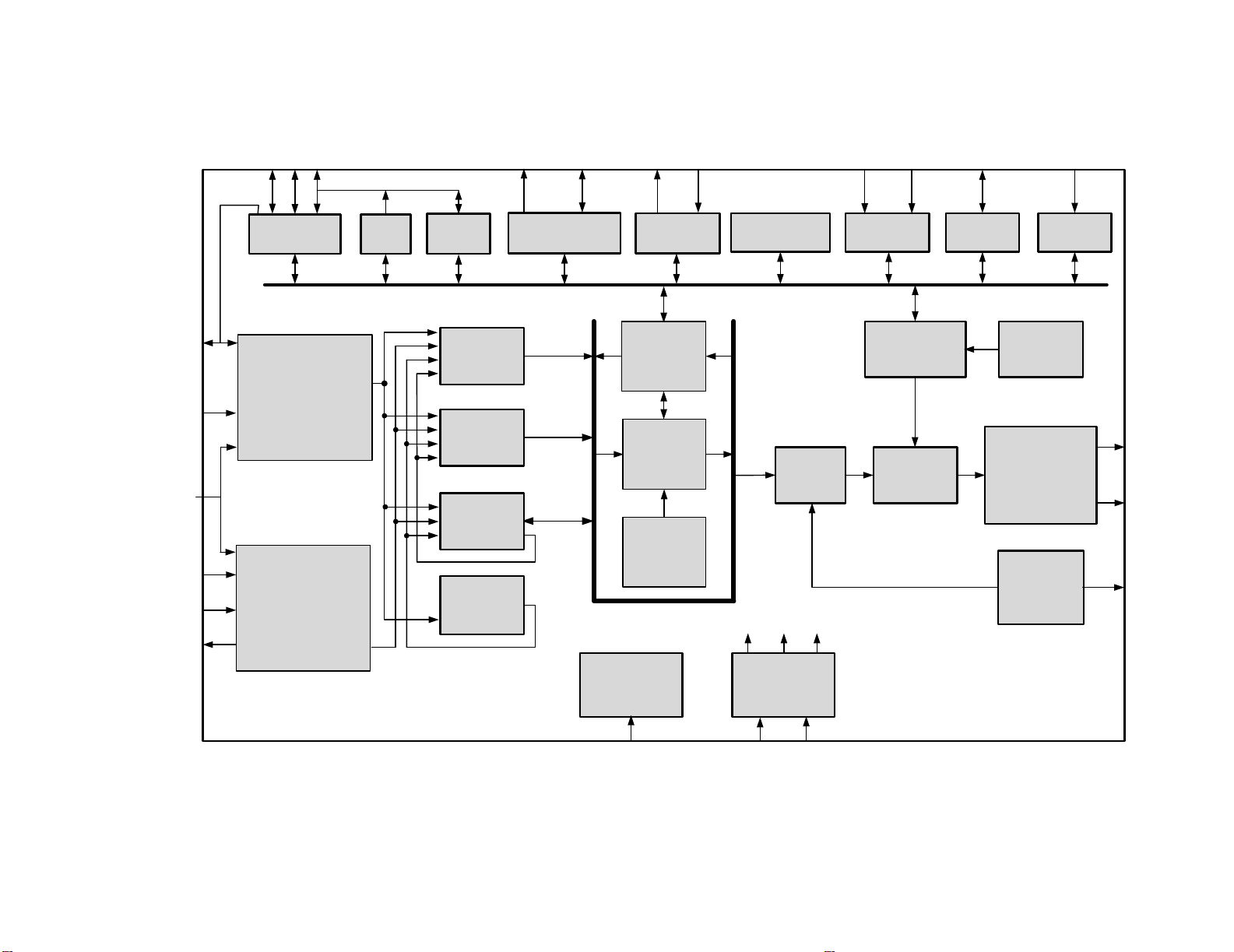
PortD(7:0)
PortE(7:0)
PortF(7:0)
PortB
PortC
(7:0)
(7:0)
GPIO PWM
PortA
(7:0)
RAMWE,
RAMOE,
ROMWE,
ROMOE
2-Wire
Serial
Microprocessor Bus
Processor ROM/
RAM Interface
A(19:0),
D(15:0),
BHEN,
CS(1:0),
RD, WR
CPUTDO
16-bit
Turbo µP
CPUTMS,
CPUTCK,
CPUTDI
Watchdog and
Timers
NMI EXTINT
Interrupt
Controller
RxD, TxD
UART
IRRCVR (1:0)
IR
Decoders
VRGB
(23:0)
VCLK, VPEN,
VVS, VHS,
Field
GCLK, GFBK,
GPEN, GVS,
GHS, GSOG
GRGB
(47:0)
GCOAST,
GREF,
GBLKSPL,
GHSFOUT
Video Port
Sync Decoder
Auto Im age
Optimizer
Color Space
Converter HDCP
Graphics Port
Sync Decoder
Auto Image
Optimizer
Color Space
Converter HDCP
Horizontal
Image
Scaler
CRISP
Image
Scaler
Video
Deinterlace
Spatial
Noise
Reduction
Bus
Memory In
Master Reset
Processor
Memory
Interface
SDRAM
Memory
Controller
Reset
Frame
Buffer
Frame
Buffer
Memory Out Bus
Image
Scaler
MCLK DCLK UCLK
Dual PLL
Clock
Generator
MCLKEXT,
XI*
XO*
OSD and CPU
SDRAM
OSD
Memory
Bus
OSD/CPU
Memory
Controller
Display Port
OSD
Control &
Blend
Color Matrix,
Gamma Correction
CLTs, Color Space
Expander
Display
Timing
Generator
PW181 Internal Block
Diagram
*For internal clock generatorDCLKEXT,
RGBE
(23:0)
RGBO
(23:0)
DVS,
DHS,
DEN,
DCLK
Figure 1-1 Internal Block Diagram
Page 24
L6B RECOMMEDED SPARE PARTS
POSITION PART NUMBER PART DESCRIPTION
056T27-CH1 LCD CHIMEI V270W1-L04 (LCD TV)
056T30-CH1 LCD CHI-MEI V296W1-L14 (LCD TV) 30")
056W26-LP2 LCD LG-PHILIPS LC260W01-A5K6 (LCD TV)
L38172 CU ASSY 30'' L6B (ZR1192-21)
L57172 CU ASSY 27'' L6B (ZR1192-21)
UR3110 L6B CHASIS 27"TOS MS/NX/3/SK/PIP/PEN/DVI
US1110 L6B CHASIS TOS 30" M/NX/3/SK/PIP/PEN/DVI
US1172 CU ASSY 30" L6BL38 TOSHIBA (ZR1191-20)
Y23172 CU ASSY 26L6L43 L6B VER.(ZP9191-20)
Y22172 CU ASSY 26L6BL44 (ZG5192-20)
Y51120 L6 CHASIS DAUGHTER BOARD
ZG4187F RC L6B TOSHIBA GRI/SHINE SI.P.ED CT-870
JX1187 R/C L6B REMOTE CONTROL JAECS SIL.GRUNDIG
ZG4301 TERMINAL BATT.BOX(+-) R/C TOSHIBA
ZJ9172 POWER SWITCH ASSY 27/30'' L6B(ZJ9192-20)
ZJ9205F BACK COVER 30'' L38 LCD TV SILVER L6B
ZJ9206F SCART BACK COVER 30L38 LCD TV SILVER
ZJ9251F FRONT COVER G.BL/BUR.SIL P.ED 30L38 TOS.
ZJ9805 CUSHION LEFT 30" LCD TV
ZJ9806 CUSHION RIGHT 30" LCD TV
ZR1107-AS SPEAKER 10W 4R PALSTIC CASE KAB MOUNTED
ZR1172 CU ASSY 27" L6BL57 TOSHIBA (ZR1191-20)
ZR1204F LENS IR/LED 30''L38 LCD TV
ZR1205F BACK COVER 27'' L57 LCD TV SILVER L6B
ZR1208F KNOB POWER 27"L57 LCD TV SILVER
ZR1212F KNOB PROGRAM/VOL. 27LCD TOSHIBA SILVER
ZR1251F FRONT COVER G.BL./BUR.SIL P.ED 27L57 TOS
ZR1255 BACK COVER DARK GRAY P.ED 27L6BL57 LCD
ZR1258 POWER KNOB BURNISH SILVER PAINTED 27"L57
ZR1805 CUSHION LEFT 30" LCD TV
ZR1806 CUSHION RIGHT 27" LCD TV
ZR1910 ADAPTOR SPS 180W 24/5 12/5 PFC 2PIN(LISH
AV/TV 010844 TACT SWITCH 2 LEG (MTSB)
CN250 031383 CON.DVI 24+5POL JRX1-DV124+5
CN601 ZJ9512-AS CABLE PANEL.INTERFACE 30"L6B CHI 30.LU
303407 LED ROT LTL 4221N P6 GREEN
303447 LED 3MM RED-BLUE LIGITEK LSRFSBK2092
F450 054290 FUSE 5.0A 250V ROUND
F451 054290 FUSE 5.0A 250V ROUND
IR1 452521-01 IR RECEIVER TSOP34838 SS1A
J19 031508 KONN. RF IEC TO RCA
J53 031477 KONN. CINCH .... WHITE HOR.12,5MM 30L6
J56 031478 KONN. CINCH ..... RED HOR.12,5MM 30L6
J57 031423 HEADPHONE JACK YKB21-5103
J832 031479 KONN. CINCH ... YELLOW HOR.12,5MM 30L6
J926 031795 KONN.S-VHS
MENU 010844 TACT SWITCH 2 LEG (MTSB)
P250 031358 CONN. VGA B10B
SAW825 056708 SAW FILTER OFW K3958M
SAW826 056708 SAW FILTER OFW K3958M
SAW827 056010 SAW FILTER OFW K9656M
Page 25
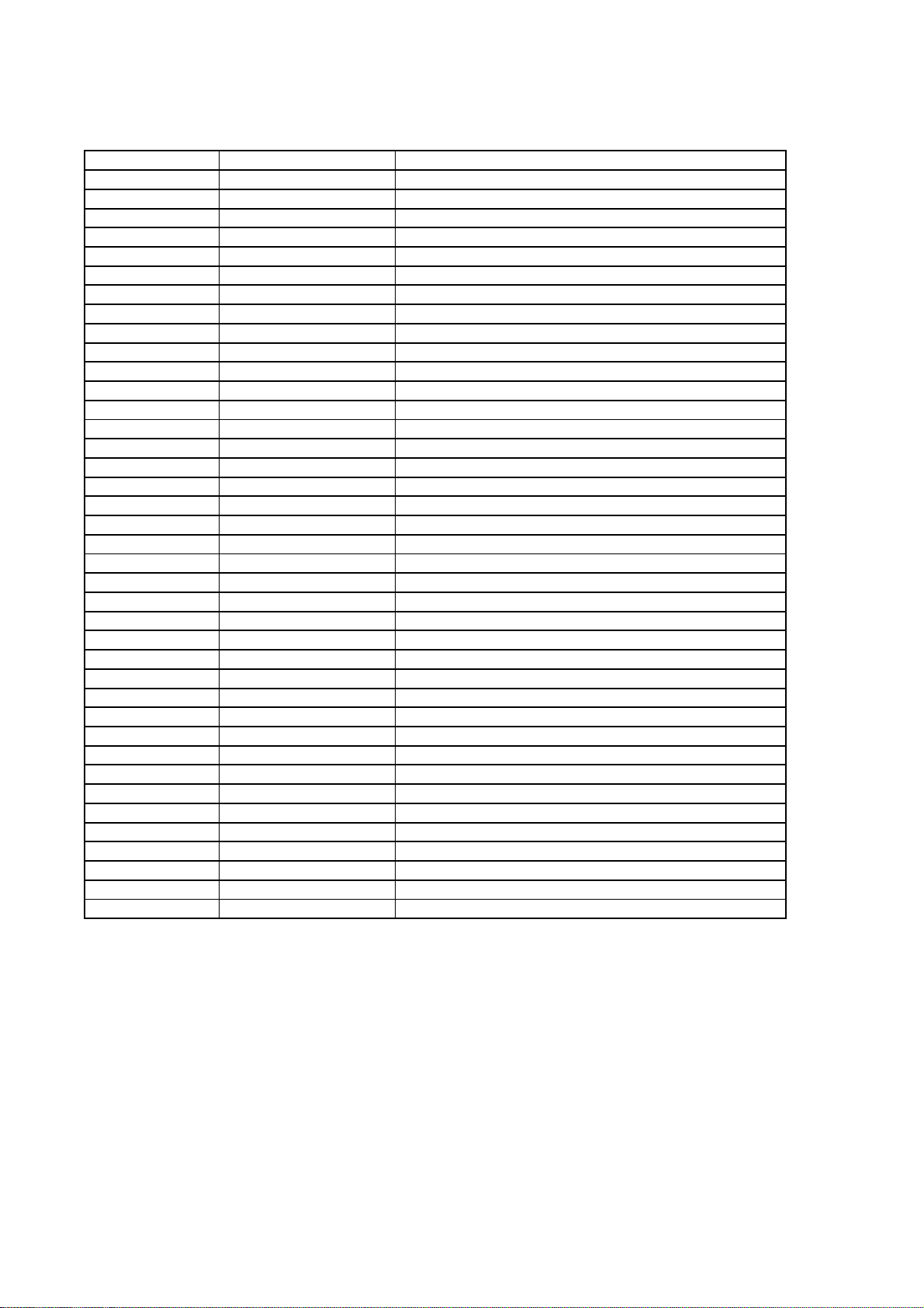
SAW828 056010 SAW FILTER OFW K9656M
SW1 010861 ON/OFF SWITCH BK98
TU825 Y51136-PH1 TUNER PH UV1316T/SIGH-3 SPL ASIMTRK YAT
TU826 Y11136 TUNER HOR.PHILLIPS UV1316/A I H-4
U1 453124 IC-CHIP NCP1117DT33RK TO-252 PACKAGE
U150 453195 IC PI5V330W SOIC(W)
U151 453350 IC-CHIP PCF8591 /SO16
U2 453262 IC-CHIP AD9887KS-100- DUAL IN.FACE TRAY
U250 453261 IC-CHIP 24LC21A-I/SN-CMOS18K/2.5V SE.T&R
U251 453261 IC-CHIP 24LC21A-I/SN-CMOS18K/2.5V SE.T&R
U3 453494 IC-CHIP TRIPATH TA2024 STEREO CLAS-D T&R
U350 453921 IC-CHIP DS90C385A MTD56
U351 452997 IC LM358DR2 / S08
U400 453233 IC-CHIP AM29LV160DB-90EC (TRAY)TSOP48
U401 453263 IC-CHIP AT24C64N-10SI-2. - SO8 TAPE&REEL
U402 453349 IC-CHIP TLC7733 /SO8
U450 453095 IC-CHIP NCP1117DTARK (DPAK)(T&R) TO252
U452 401372 TRN FDS9933A
U454 453294 IC-CHIP LM2576D2TR4-005V 3A TO263 STPT&R
U455 453294 IC-CHIP LM2576D2TR4-005V 3A TO263 STPT&R
U456 453428 IC-CHIP LM317MDT VAR.VOLT.REG. TO-252
U457 453124 IC-CHIP NCP1117DT33RK TO-252 PACKAGE
U458 453124 IC-CHIP NCP1117DT33RK TO-252 PACKAGE
U50 452706 IC TDA1308T/N1 SO-G8 (T&R)
U51 453352 IC-CHIP MSP3410-MQFP64
U52 453351 IC TEA6420 /SO28
U650 453346 IC-CHIP PW1231A
U750 452863 IC MT48LC4M16A2-7E SDRAM 54PIN TSOP
U825 451569 IC-CHIP TDA9886T/V3 118(SO24) T&R
U826 451569 IC-CHIP TDA9886T/V3 118(SO24) T&R
U827 453271 IC-CHIP TEA6415CDT -VIDEO-MAT-SW.T&R
U925 453124 IC-CHIP NCP1117DT33RK TO-252 PACKAGE
X941 8R9185 HP JACK 17"LCD TV
Y300 056753 CRYSTALL 24.576MHZ 20PF 30PPM
Y50 056952 CRYSTAL 18.432MHZ +-30PPM
Y550 056119 CRYSTAL 14.31818MHz CL=18PF30/30PPMHC49U
Y650 056121 CRYSTAL 10 MHz / HC49U 20PF 30PPM
Y825 056013 CRYSTAL 4 MHZ HC49-U
Y826 056013 CRYSTAL 4 MHZ HC49-U
Y925 056753 CRYSTALL 24.576MHZ 20PF 30PPM
Page 26
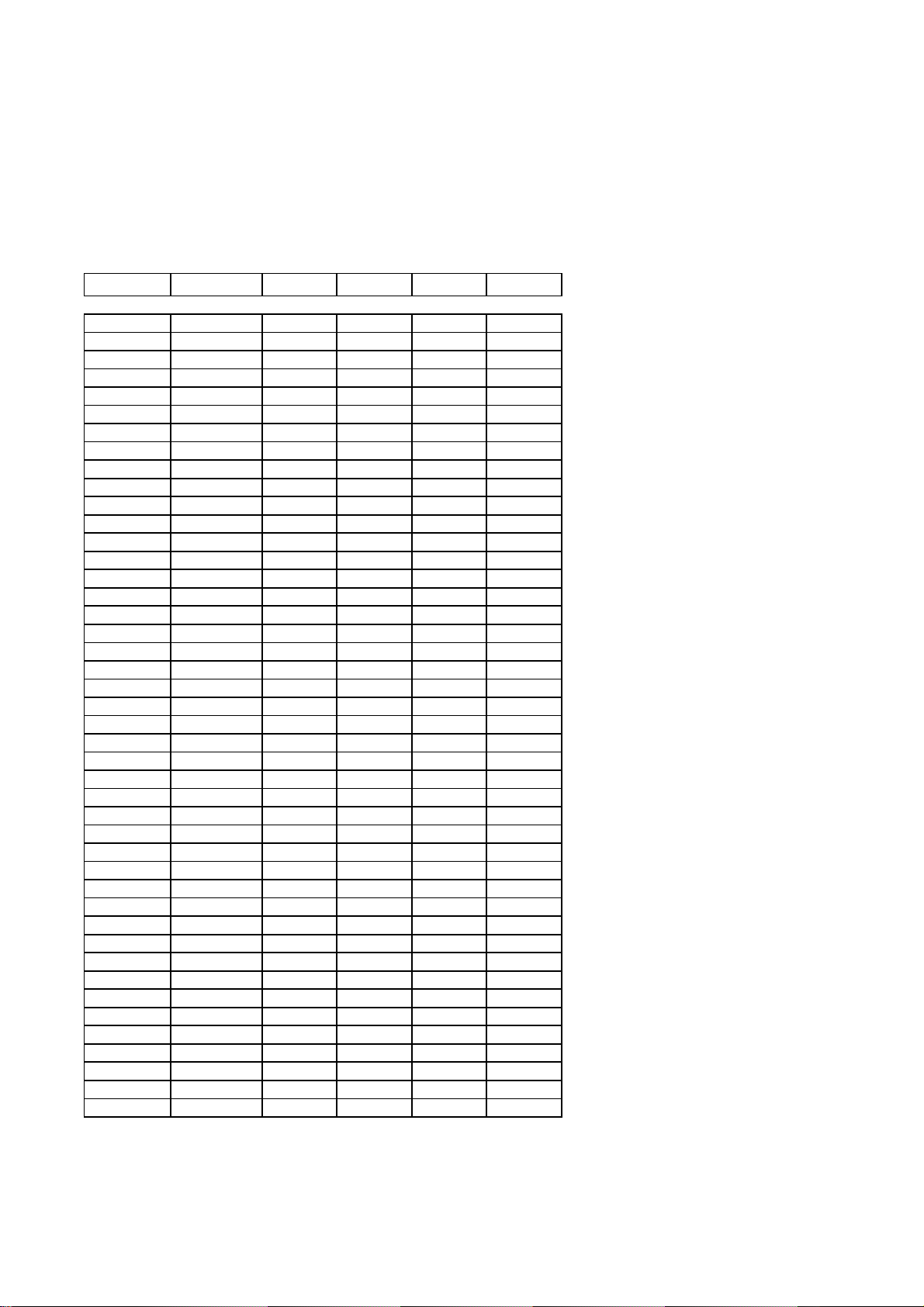
FREQUENCY TABLE (MHz)
Channel Number BG I DK L/L'
CH 1 49.75 49.75 47.75
CH 2 48.25 59.25 59.25 55.75
CH 3 55.25 77.25 77.25 60.50
CH 4 62.25 85.25 85.25 63.75
CH 5 175.25 93.25 93.25 176.00
CH 6 182.25 175.25 175.25 184.00
CH 7 189.25 183.25 183.25 192.00
CH 8 196.25 191.25 191.25 200.00
CH 9 203.25 199.25 199.25 208.00
CH 10 210.25 207.25 207.25 216.00
CH 11 217.25 215.25 215.25 189.25
CH 12 224.25 223.25 223.25 182.25
CH 13 53.75 45.75 196.25
CH 14 62.25 53.75 210.25
CH 15 82.25 61.75
CH 16 175.25 69.75
CH 17 183.25 95.25
CH 18 192.25
CH 19 201.25
CH 20 210.25
CH 21 471.25 471.25 471.25 471.25
CH 22 479.25 479.25 479.25 479.25
CH 23 487.25 487.25 487.25 487.25
CH 24 495.25 495.25 495.25 495.25
CH 25 503.25 503.25 503.25 503.25
CH 26 511.25 511.25 511.25 511.25
CH 27 519.25 519.25 519.25 519.25
CH 28 527.25 527.25 527.25 527.25
CH 29 535.25 535.25 535.25 535.25
CH 30 543.25 543.25 543.25 543.25
CH 31 551.25 551.25 551.25 551.25
CH 32 559.25 559.25 559.25 559.25
CH 33 567.25 567.25 567.25 567.25
CH 34 575.25 575.25 575.25 575.25
CH 35 583.25 583.25 583.25 583.25
CH 36 591.25 591.25 591.25 591.25
CH 37 599.25 599.25 599.25 599.25
CH 38 607.25 607.25 607.25 607.25
CH 39 615.25 615.25 615.25 615.25
CH 40 623.25 623.25 623.25 623.25
CH 41 631.25 631.25 631.25 631.25
CH 42 639.25 639.25 639.25 639.25
CH 43 647.25 647.25 647.25 647.25
CH 44 655.25 655.25 655.25 655.25
Page 27
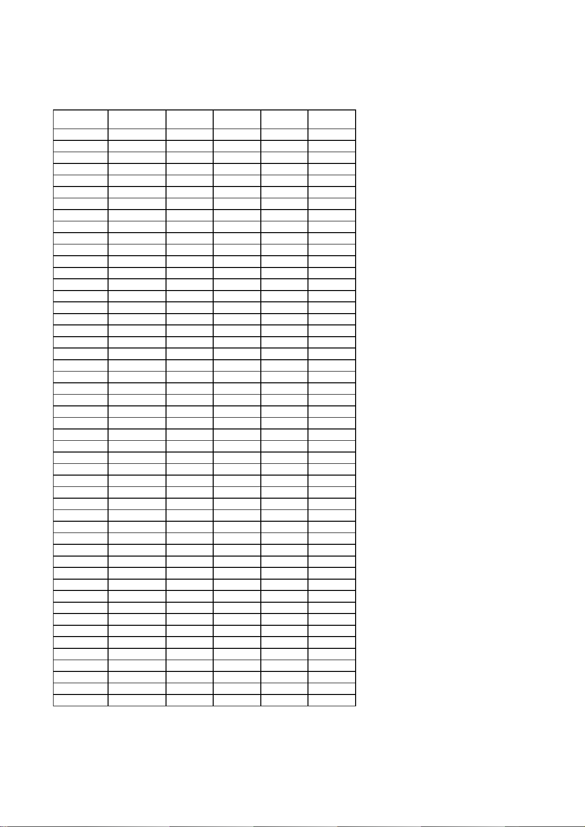
Channel Number BG I DK L/L'
CH 45 663.25 663.25 663.25 663.25
CH 46 671.25 671.25 671.25 671.25
CH 47 679.25 679.25 679.25 679.25
CH 48 687.25 687.25 687.25 687.25
CH 49 695.25 695.25 695.25 695.25
CH 50 703.25 703.25 703.25 703.25
CH 51 711.25 711.25 711.25 711.25
CH 52 719.25 719.25 719.25 719.25
CH 53 727.25 727.25 727.25 727.25
CH 54 735.25 735.25 735.25 735.25
CH 55 743.25 743.25 743.25 743.25
CH 56 751.25 751.25 751.25 751.25
CH 57 759.25 759.25 759.25 759.25
CH 58 767.25 767.25 767.25 767.25
CH 59 775.25 775.25 775.25 775.25
CH 60 783.25 783.25 783.25 783.25
CH 61 791.25 791.25 791.25 791.25
CH 62 799.25 799.25 799.25 799.25
CH 63 807.25 807.25 807.25 807.25
CH 64 815.25 815.25 815.25 815.25
CH 65 823.25 823.25 823.25 823.25
CH 66 831.25 831.25 831.25 831.25
CH 67 839.25 839.25 839.25 839.25
CH 68 847.25 847.25 847.25 847.25
CH 69 855.25 855.25 855.25 855.25
CH 70 863,25 863.25
CH 71 871,25
CH 72 879,25
CH 73 887,25 160.00
CH 74 69.25 172.00
CH 75 76.25 220.00
CH 76 83.25 232.00
CH 77 90.25 244.00
CH 78 97.25 256.00
CH 79 59.25 268.00
CH 80 93.25 280.00
S 1 105.25 103.25 103.25 116.75
S 2 112.25 111.25 111.25 128.75
S 3 119.25 119.25 119.25 140.75
S 4 126.25 127.25 127.25 152.75
S 5 133.25 135.25 135.25 164.75
S 6 140.25 143.25 143.25 176.75
S 7 147.25 151.25 151.25 188.75
S 8 154.25 159.25 159.25 200.75
S 9 161.25 167.25 167.25 212.75
S 10 168.25 231.25 231.25 224.75
S 11 231.25 239.25 239.25 236.75
S 12 238.25 247.25 247.25 248.75
S 13 245.25 255.25 255.25 260.75
S 14 252.25 263.25 263.25 272.75
Page 28
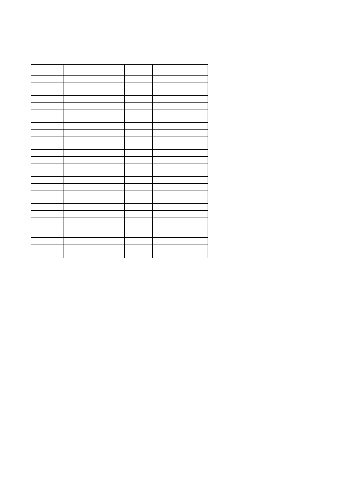
Channel Number BG I DK L/L'
S 15 259.25 271.25 271.25 284.75
S 16 266.25 279.25 279.25 296.75
S 17 273.25 287.25 287.25 55.75
S 18 280.25 295.25 295.25 60.50
S 19 287.25 303.25 303.25 63.75
S 20 294.25
S 21 303.25 303.25
S 22 311.25 311.25 311.25 311.25
S 23 319.25 319.25 319.25 319.25
S 24 327.25 327.25 327.25 327.25
S 25 335.25 335.25 335.25 335.25
S 26 343.25 343.25 343.25 343.25
S 27 351.25 351.25 351.25 351.25
S 28 359.25 359.25 359.25 359.25
S 29 367.25 367.25 367.25 367.25
S 30 375.25 375.25 375.25 375.25
S 31 383.25 383.25 383.25 383.25
S 32 391.25 391.25 391.25 391.25
S 33 399.25 399.25 399.25 399.25
S 34 407.25 407.25 407.25 407.25
S 35 415.25 415.25 415.25 415.25
S 36 423.25 423.25 423.25 423.25
S 37 431.25 431.25 431.25 431.25
S 38 439.25 439.25 439.25 439.25
S 39 447.25 447.25 447.25 447.25
S 40 455.25 455.25 455.25 455.25
S 41 463.25 463.25 463.25 463.25
Page 29
Page 30
Page 31
Page 32
Page 33
Page 34
Page 35
Page 36
Page 37
Page 38
Page 39
 Loading...