

Page 1

RAK410 DataSheet
1
RAK410 Serial WIFI Module Data Sheet
Page 2

RAK410 DataSheet
2
V0.4.4
Initial Draft
2012-9-26
1 Overview
1.1 Revision History
1.2 General Description
RAK410 module is an ultra-low power WIFI module that fully supports IEEE 802.11b/g/n wireless standards,
with a small package and easy-to-use features. The module supports connecting to devices via UART and SPI
interfaces, and is internally integrated TCP / IP protocol stack. Hence it facilitates rapid development. In order to
adapt to a variety of application environments, RAK410 module is extended into four sub-types: RAK410A,
RAK410B, RAK410-1A, and RAK410-1B.
RAK410A:Supports UART interface, with on-board antenna;
RAK410B:Supports UART interface, with U-FL connector to connect to an external antenna.
RAK410-1A:Supports SPI interface, with on-board antenna;
RAK410-1B:Supports SPI interface, with U-FL connector to connect to an external antenna.
1.3 Key Applications
Portable products
Home appliances and electrical appliances
Industrial sensors
Sales terminals
Buildings automation
Logistics and freight management
Home security and automation
Medical applications, such as patient monitoring, medical diagnostics
Metering (stop timing, measuring instruments, meters, etc.)
1.4 Devices Features
Support IEEE 802.11b/g/n wireless standards
Integrated TCP / IP protocol stack
Support OPEN, WEP, WPA/WPA2-PSK Encryptions
Support Station mode and Ad-Hoc mode
Support TCP, UDP protocols
Support DHCP SERVER / DHCP CLIENT
Support AT commands and transparent transmission mode
Page 3
RAK410 DataSheet
3
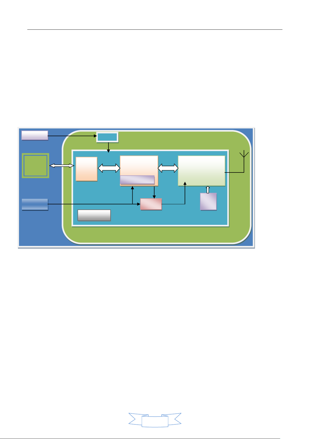
UART
MCU
TCP/IP STACK
CLOCK
Management
LDO1.8V
Wi-Fi
HOST
Reset_n
3.3V
Supply
Reset
UART/
SPI
Flash
Support UART/SPI interfaces
Support UART communication with a data flow control, maximum rate of 921600bps
On-board ceramic antenna or U.FL antenna connector
Operating voltage: 3.3V
Support 3 kinds of power operating mode, with the lowest power consumption of 0.5uA
Small package size: 23.14mm × 28.75mm
FCC, RoHS and CE compliant
1.5 RAK410 System Diagram
2 Functional Description
2.1 Interface
UART
Rate: 9600 ~ 921600bps
Support hardware flow control
SPI
Work mode: slave mode
Maximum clock frequency: 4MHz
Configurable clock polarity and clock phase
Page 4
RAK410 DataSheet
4
2.2 Wi-Fi
Comply with IEEE 802.11b/g/n standards
Support WEP, WPA/WPA2-PSK encryptions
Support QoS
Support Infrastructure and Ad-hoc Modes
2.3 Network Protocols
TCP
UDP
ARP
ICMP
DHCP Client
DHCP Server
3 Hardware Introduction
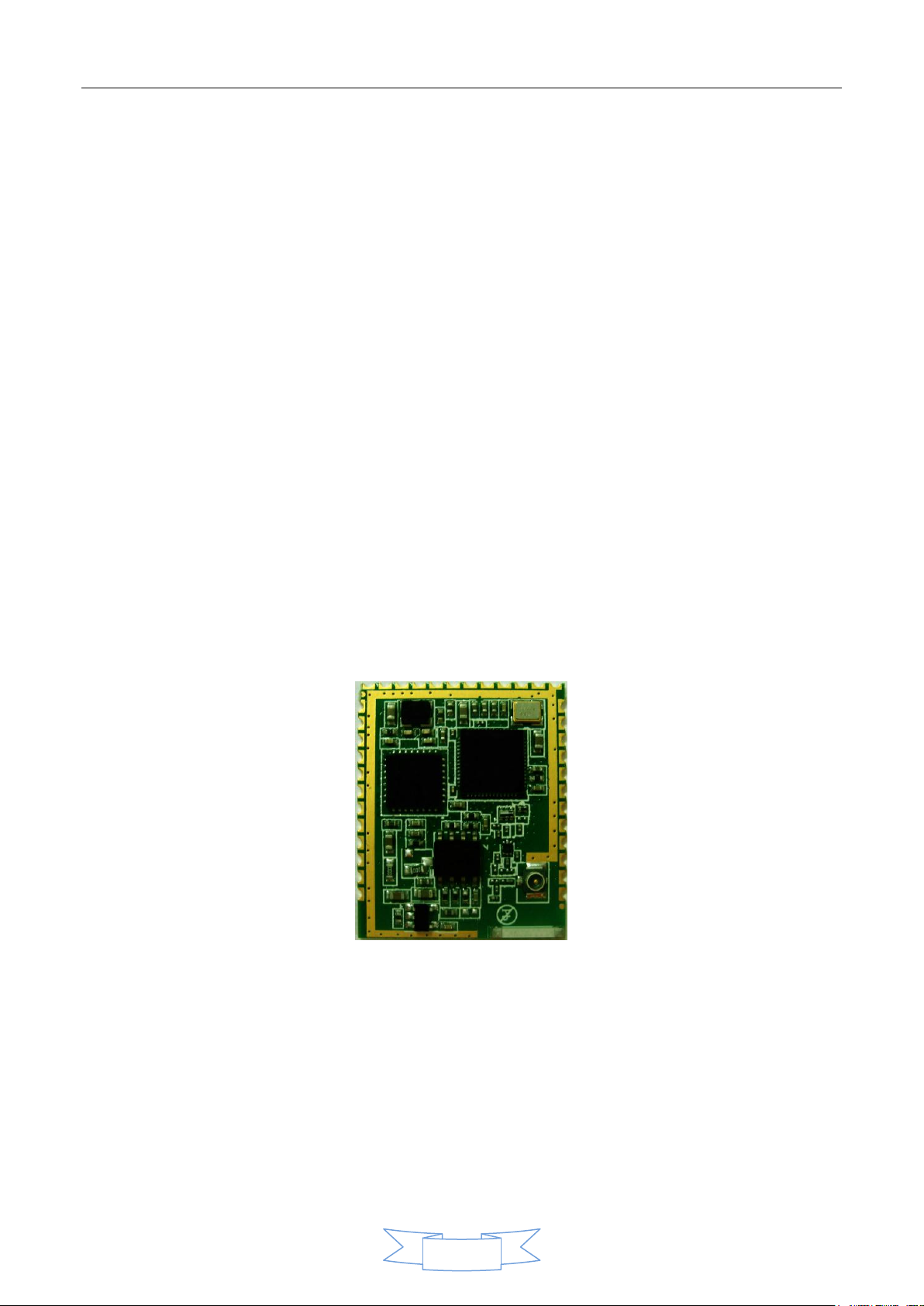
3.1 Top View
Figure 1: Module Top View
Page 5
RAK410 DataSheet
5
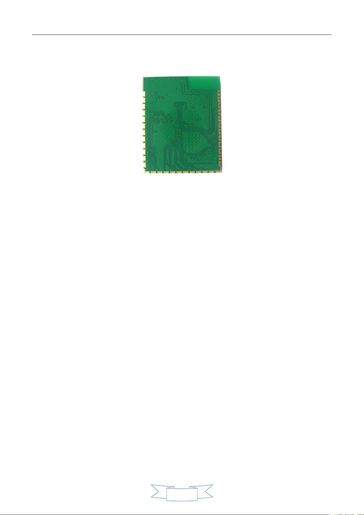
3.2 Bottom View
Figure 2: Module Bottom View
Page 6
RAK410 DataSheet
6
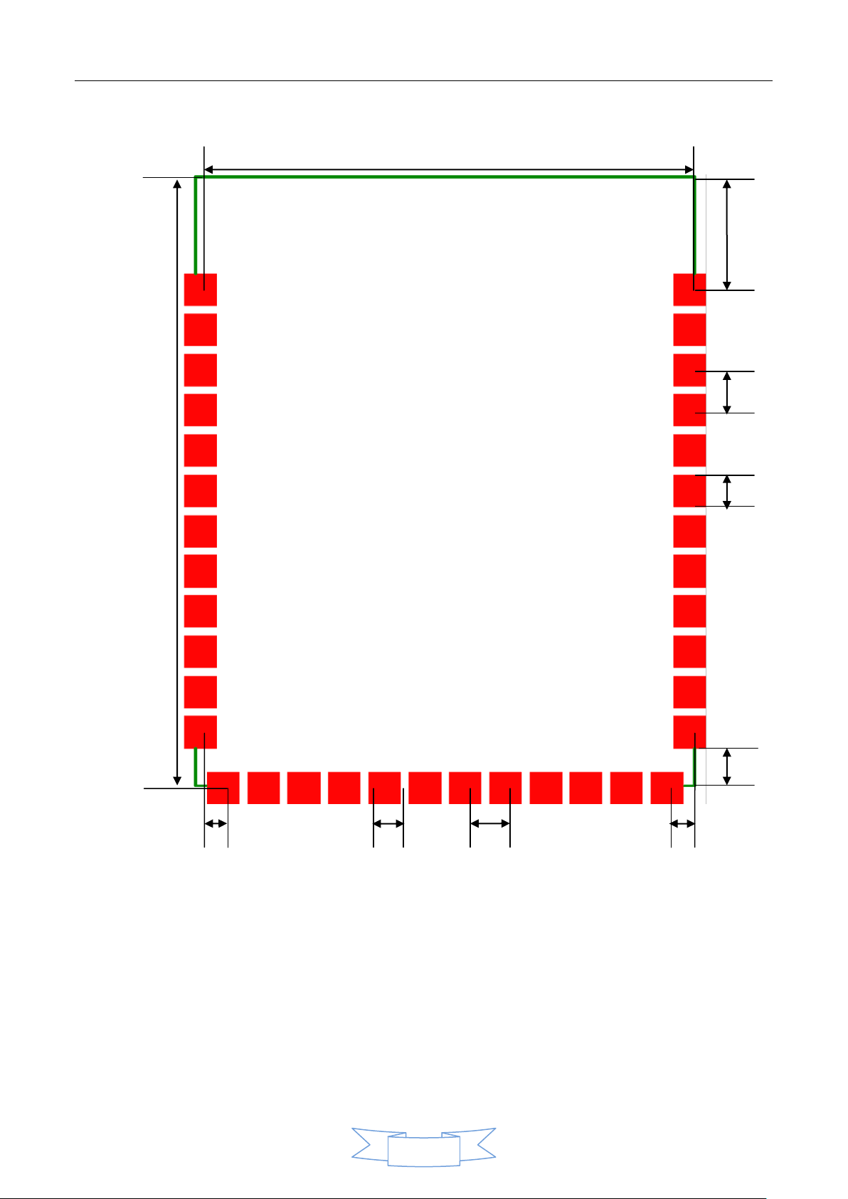
1140
910
210
75
60
105
43
43
60
75
3.3 PCB Mechanical Size
Figure 4: PCB Pins Size (Bottom View)
(Unit:mil)
Page 7
RAK410 DataSheet
UART_RTS/SPI_CLK
UART_CTS/SPI_CS
MCU_BOOT
SYS_ERROR
R4
10Kohm
U1 RAK410_A
GND1GND
2
NC
3
NC
10
NC
11
GND12GND
13
NC
14
NC
15
NC
16
NC
17
MCU_ERROR
18
MCU_RESET
19
NC
20
NC
21
NC
22
WPS
23
NC
24
GND
5
BIAS
4
NC
9
MCU_MODE
8
NC
6
NC
7
GND
25
NC
26
MCU_SPI_INT
27
MCU_BOOT
28
NC
29
NC
30
MCU_US0_TX
31
MCU_US0_RX
32
MCU_US0_CLK
33
MCU_US0_CS
34
VCC3V3
35
GND
36
Host Power Supply
R1
1Mohm/NL
C1
10uF
VDD33
VDD33
C2
0.1uF
UART_TX/SPI_MOSI
R2
1Mohm/NL
MCU_MODE
WPS
R3
10Kohm/NL
VDD33
MCU_RESET
UART_RX/SPI_MISO
MCU_SPI_INT
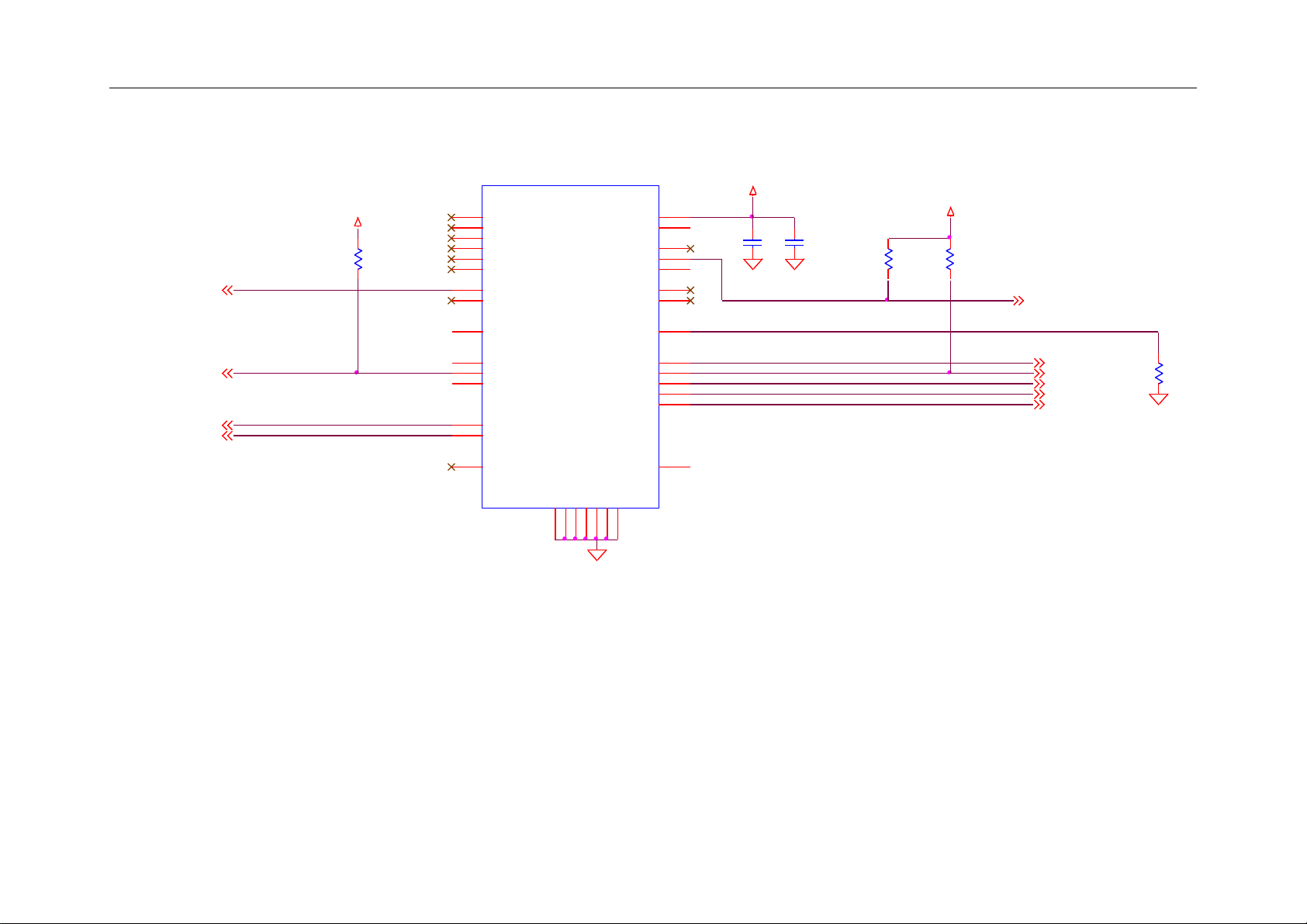
3.4 Design Reference
Note:R1, R2, R3 are 10kΩ; C1 is 10μF; C2 is 0.1μF.
Figure 5:RAK410 Module Peripheral Design Reference
Page 8
RAK410 DataSheet
8
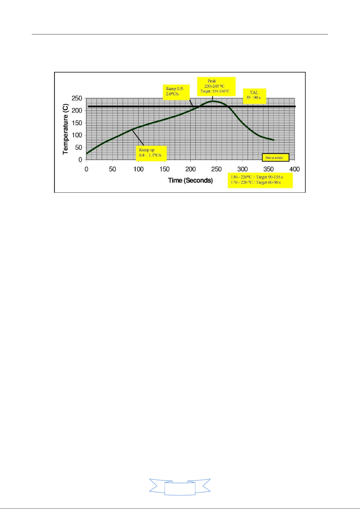
3.6 Reflow Soldering Temperature Graph
Figure 6: Temperature Graph
Note: as shown in Figure 6, it is based on the SAC305 lead-free tin paste (3% silver, 0.5% copper).
Alpha OM-338 lead-free cleaning-free flux is recommended. The Figure 6 is mainly used for guidance.
The entire process time is subject to thermal pad number of assembly board and device Intensity.
3.7 Baking Instructions
The RAK410 module is very sensitive to water. Be cautious to baking the device. At ambient conditions, it is
required that within 168 hours removed from the vacuum packaging, the module should be processed with the
circuit board assembly by reflow soldering; Or stored in the environment with a relative humidity below 10%. If
the condition is not satisfied, the RAK410 must be processed with a 9-hour baking in the environment of 125 ℃
before the reflow soldering.
Page 9
RAK410 DataSheet
9
Pin Serial
No.
Name
Description
Type
1
GND
Ground
P 2 GND
Ground
P 3 NC
No connect (Reserved)
- 4 BIAS
Bias pin, 10K resistor to the ground
I 5 GND
Ground
P
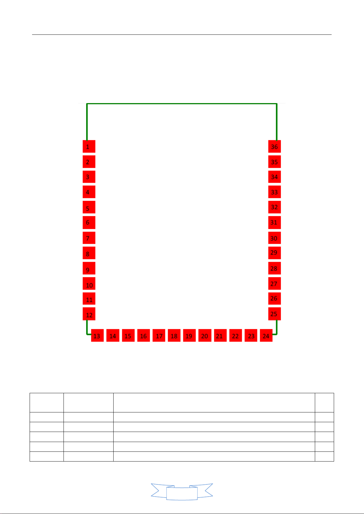
4 Pins Definition
4.1 Module Pins(Top View)
4.2 Pin Definition
Figure 7: Module Pins Map
Page 10

RAK410 DataSheet
10
6
NC
No connect (Reserved)
- 7 NC
No connect (Reserved)
-
8
MCU_MODE
If parameters saving is enabled,
MCU_MODE=1, enter into transparent transmission mode
MCU_MODE=0, enter into Command line mode
I
9
NC
No connect (Reserved)
-
10
NC
No connect (Reserved)
-
11
NC
No connect (Reserved)
-
12
GND
Ground
P
13
GND
Ground
P
14
NC
No connect (Reserved)
-
15
NC
No connect (Reserved)
-
16
NC
No connect (Reserved)
-
17
NC
No connect (Reserved)
-
18
MCU_ERROR
In Transparent Transmission mode, it is used to indicate the module when
running error, high storage is valid.
O
19
MCU_RESET
Reset module, low storage is valid.
I
20
NC
No connect (Reserved)
-
21
NC
No connect (Reserved)
-
22
NC
No connect (Reserved)
-
23
NC
No connect (Reserved)
-
24
NC
No connect (Reserved)
-
25
GND
Ground
-
26
NC
No connect (Reserved)
-
27
NC
No connect (Reserved)
-
28
MCU_BOOT
It is used to enter the boot program, high storage is valid.
I
29
NC
No connect (Reserved)
-
30
NC
No connect (Reserved)
-
31
MCU_UART_TX
UART data transmit
O
MCU_SPI_MOSI
SPI data receive
I
32
MCU_ UART
_RX
UART data receive
I
MCU_SPI_MISO
SPI data transmit
O
33
MCU_UART_RTS
UART transmit request
O
MCU_SPI_CS
SPI chip select input
I
34
MCU_UART_CTS
UART transmit clear
I
MCU_SPI_CLK
SPI clock input
I
35
VCC3V3
Operating voltage input (3.3V)
P
36
GND
Ground
P
Table 1: Pin Definition
Page 11
RAK410 DataSheet
11
Parameters
Symbols
Value
Unit
External supply voltage
VCC3V3
-0.3~4.0
V
Maximum RF Input (Reference: 50Ω )
RF
in
+10
dBm
When voltage is 3.3V, IO Max voltage
3V3VinIOMax
VCC+0.3
V
When voltage is 3.3V, IO Min voltage
3V3VinIOMin
-0.3
V
Storage ambient temperature
T
store
-65~+135 ℃ ESD resistance
ESD
HBM
2000
V
Parameters
Symbols
Min Value
Typical Value
Max Value
Unit
External voltage
Vcc
3.14
3.3
3.46
V
Ambient temperature
T
ambient
-20
--
TBD
℃
Parameters
Test conditions
Typical Value
Unit
Receiver sensitivity
11b,1Mbps
-97
dBm
11b,2Mbps
-92
dBm
11b,5.5Mbps
-90
dBm
11b,11Mbps
-88
dBm
11g,9Mbps
-91
dBm
11g,18Mbps
-87
dBm
11g,36Mbps
-81
dBm
11g,54Mbps
-75
dBm
11n,MCS1,13Mbps
-89
dBm
11n,MCS3,26Mbps
-82
dBm
11n,MCS5,52Mbps
-75
dBm
11n,MCS7,65Mbps
-72
dBm
Maximum input signal
CH7
11g,54Mbps
10
dBm
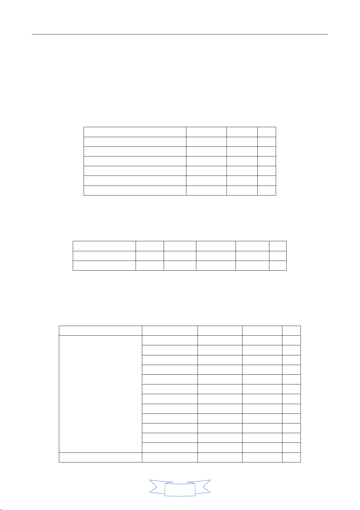
5 Electrical Characteristics
5.1 Absolute Maximum
The following table shows the absolute maximum. Note that the module device may be damaged when exceeds
the maximum. To avoid damages to the module and the device, please operate under specified conditions.
Table 2: Parameters and Value Range
5.2 Recommended Operating Parameters
Table 3: Recommended Operating Parameter Range
5.3 RF Electrical Characteristics
RF Receiver Specifications
Page 12
RAK410 DataSheet
12
Adjacent channel suppression
6Mbps
37
dBc
54Mbps
21
dBc
MCS0
38
dBc
MCS7
20
dBc
Symbol
Parameters
Requirements
Typical Value
Unit
F
tx
Frequency range
--
2.4
GHz
P
out
Output power
--
--
--
802.11b
1Mbps
17
dBm
802.11g
6Mbps
17
dBm
802.11n,HT20
MCS0
17
dBm
802.11g,EVM
54Mbps
14
dBm
802.11n,HT20EVM
MCS7
10
dBm
Symbol
Description
typical(μ S)
T
RESET
MCU reset pulse length
100
RF Transmit Specifications
Table 4: Partial RF Receiver Specifications
Table 5: Partial RF Transmit Specifications
5.4 MCU Reset
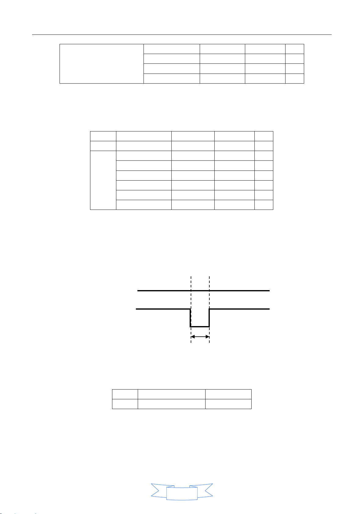
Figure 8 shows the MCU reset timing diagram and reset pulse length.
3.3V IO Supply
MCU_RESET
T
Figure 8: MCU Reset Timing
Table 6 shows the description of MCU reset parameters.
RESET
Table 6: MCU Reset Parameters
Page 13

RAK410 DataSheet
13
Operating Mode
Work State
Power Consumption
Disconnecting to AP, no
data is sent
Connecting to AP
(beacon=100ms),
no data is sent
Power Mode 0
Normal
80.4mA
80.4mA
Power Mode1
Standby
2.4mA
5.8mA
Deep sleep
2mA
2mA
Power Mode2
Standby
0.4mA
2.9mA
Deep sleep
0.5uA
0.5uA
6 Software Overview
6.1 Functional Description
By sending AT commands via UART / SPI, RAK410 completes module configurations, which include wireless
network scan, password entering and network connection, establishment of TCP / UDP connection and data
transmit.
6 .2 Software Features
Support TCP, UDP protocols
Support PING command
Support DHCP SERVER / DHCP CLIENT
Support command transmission mode and transparent transmission mode when send data
Support configuration parameters saving; through pin control, the module can enter directly into the
transparent transmission mode after powered
Support disconnected TCP automatically reconnection, disconnected wireless automatically reconnection
in transparent transmission mode,
6 Power Management
6.1 Functional Description
As the following figure shows, RAK410 supports three kinds of power operating mode:
Figure 6: Operating Mode and the Corresponding Power Consumption
Page 14

RAK410 DataSheet
14
6.1.1 Power Mode 0
In power Mode 0, RAK410 module operates at the best performance, and the wireless part and control part
completely open.
6.1.1 Power Mode 1
The Power Mode 1 has two states: Standby and Deep sleep.
In Standby state, the wireless part will enter into a low-power status, where it reduces power consumption by
accepting Beacon signals at a fixed time interval, the longer the time interval, the lower the power consumption is,
but the delay of the wireless part of the reaction will be longer; In Standby state, the control part will enter into a
low-power status as well, and the host can quickly wake this part by command and sending and receiving data.
In Deep sleep state, the module will turn off the power of the wireless part. Therefore, in this state the
wireless part has the lowest power consumption. The host can restore the task status control from what was
before the closure by specific commands, but the wake-up time will be longer; In Deep sleep state, the control
part will enter into a low-power consumption status too, and the host can quickly wake this part by command and
sending and receiving data.
6.1.2 Power Mode 2
The Power Mode 2 has two states: Standby and Deep sleep.
In Standby state, the wireless part will enter into a low-power status, where it reduces power consumption by
accepting Beacon signals at a fixed time interval, the longer the time interval, the lower the power consumption is,
but the delay of the wireless part of the reaction will be longer; In Standby state, the host can make the control
part to enter into a deep sleep status by commands, the host can only wake this part via UART_CTS pin or via
sending data through wireless to the module.
In Deep sleep state, the module will turn off the power of the wireless part. Therefore, in this state the
wireless part has the lowest power consumption. The host can restore the task status control from what was
before the closure by specific commands, but the wake-up time will be longer; In Standby state, the host can make
the control part to enter into a deep sleep status by commands, the host can only wake this part via UART_CTS pin
or via sending data through wireless to the module.
Product Information
Product Models:
RAK410A (UART interface module, internal antenna)
RAK410B (UART interface module, external antenna)
RAK410-1A (SPI interface module, internal antenna)
RAK410-1B (SPI interface module, internal antenna)
Packaging: pallet packing
Page 15

RAK410 DataSheet
15
Part Number
Antenna Type
Anteenna Gain
DTS mode
7598-r4
CHIP
0dBi
Approved
7598-r7
male/female/SMT connector
0dBi
Approved
Antenna Selection
In order to maintain compliance with FCC regulations, an antenna with no more than 0 dBi gain must be used.
This module has been tested with the following antennas:
FCC Caution: Any changes or modifications not expressly approved by the party responsible for compliance
could void the user's authority to operate this equipment.
This device complies with Part 15 of the FCC Rules. Operation is subject to the following two conditions: (1)
This device may not cause harmful interference, and (2) this device must accept any interference received,
including interference that may cause undesired operation.
This device and its antenna(s) can not be installed and operating in conjunction with any other antenna or
transmitter.
Note: This equipment has been tested and found to comply with the limits for a Class B digital device,
pursuant to part 15 of the FCC Rules. These limits are designed to provide reasonable protection against harmful
interference in a residential installation. This equipment generates uses and can radiate radio frequency energy
and, if not installed and used in accordance with the instructions, may cause harmful interference to radio
communications. However, there is no guarantee that interference will not occur in a particular installation. If this
equipment does cause harmful interference to radio or television reception, which can be determined by turning
the equipment off and on, the user is encouraged to try to correct the interference by one or more of the
following measures:
-Reorient or relocate the receiving antenna.
-Increase the separation between the equipment and receiver.
-Connect the equipment into an outlet on a circuit different from that to which the receiver is connected.
-Consult the dealer or an experienced radio/TV technician for help.
This equipment complies with FCC radiation exposure limits set forth for an uncontrolled environment. This
equipment should be installed and operated with minimum distance 20cm between the radiator & your body
The module must not be modified in any way. Coupling of external circuitry
must not bypass the provided connectors.
End product must be externally labeled with “Contains FCC ID: RGLRAKE410”
The integrator must not provide any information to the end-user on how to
install or remove the module from the end-product.
 Loading...