


BEIJING JIA AN ELECTRONIC TECHNOLOGY CO,.LTD. TA3200R1D-UFL User Manual
V1.0
http://www.rf-products.com Apr. 13th 2015
—————————————————————————————————————————————
TA3200R1D-UFL User Manual V1.0
BEIJING JIA AN ELECTRONIC TECHNOLOGY CO,.LTD.
- 1 -

BEIJING JIA AN ELECTRONIC TECHNOLOGY CO,.LTD. TA3200R1D-UFL User Manual
V1.0
http://www.rf-products.com Apr. 13th 2015
—————————————————————————————————————————————
Date Revision Description
Apr.13th 2015 V1.0
- 2 -
BEIJING JIA AN ELECTRONIC TECHNOLOGY CO,.LTD. TA3200R1D-UFL User Manual
V1.0
http://www.rf-products.com Apr. 13th 2015
—————————————————————————————————————————————
~+75℃
Description
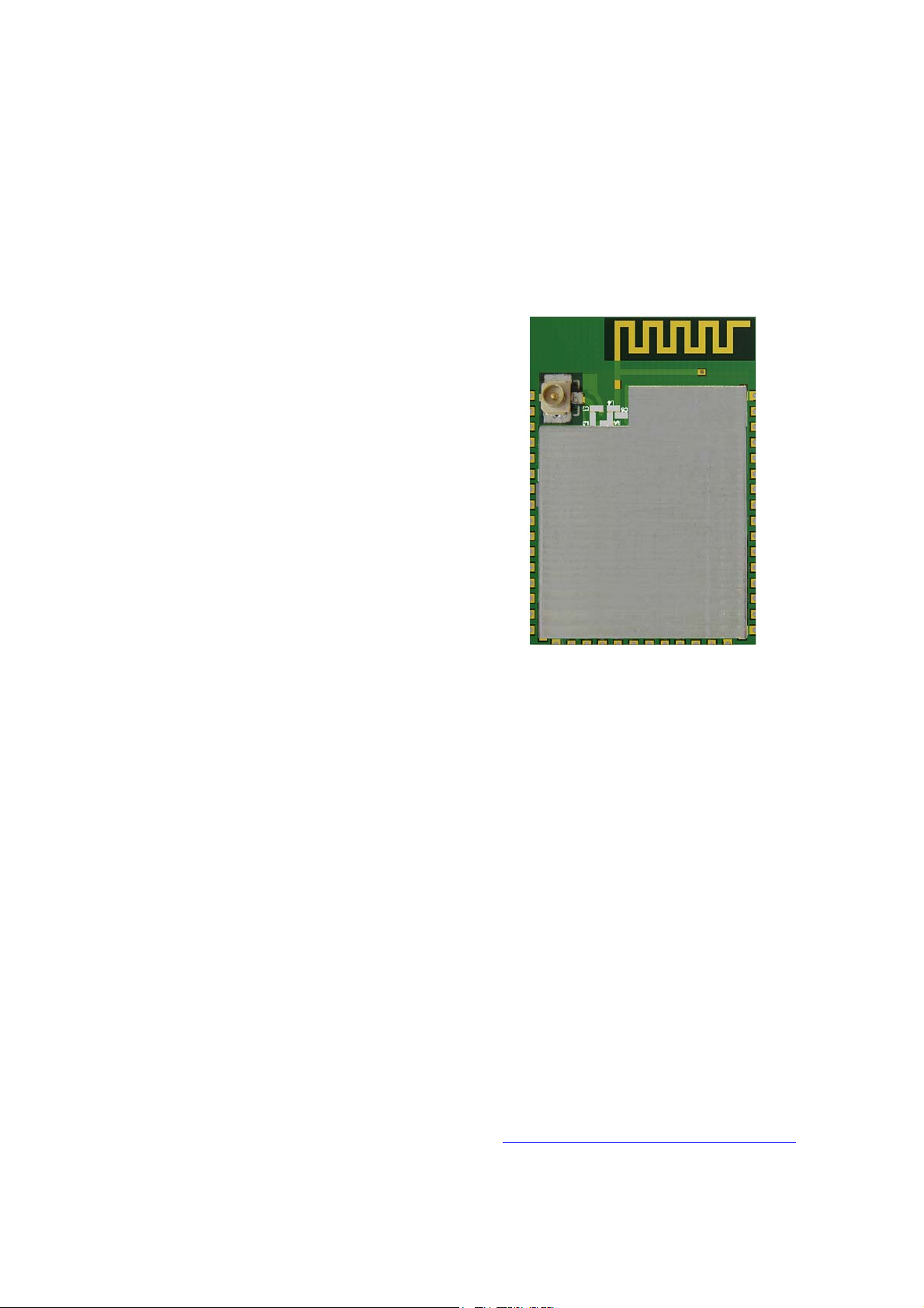
TA3200R1D-UFL Module is a
low-power module includes an 802.11 b/g/n
radio, baseband, and MAC, which is
designed for the application of wireless
network communication with embedded
technology. Using this module user can
connect physical device to Wi-Fi Network,
and then realize the control and
management of the Internet of Things. The
core of the module is CC3200 launched by
TI. CC3200 device is a wireless MCU that
integrates a high-performance ARM
Cortex-M4 core running at 80MHz, includes
embedded TCP/IP and TLS/SSL stacks,
HTTP Server, and multiple Internet
protocols, allowing customers to develop
an entire application with a single IC.
Package:18.22mm*26.65mm*2.8mm
Features
ARM Cortex -M4 Core at 80 MHz ARM
Core
includes a wide variety of peripherals
Wi-Fi and Internet Protocols in ROM
802.11 b/g/n Radio, Baseband, Medium
Access Control (MAC), Wi-Fi Driver, and
Supplicant
Station, AP, and Wi-Fi Direct Modes
TX Power:
18.0 dBm @ 1 DSSS
14.5 dBm @ 54 OFDM
RX Sensitivity:
-95.7 dBm @ 1 DSSS
-74.0 dBm @ 54 OFDM
Power-Management Subsystem:
V BATWide-Voltage Mode: 2.2 to 3.6 V
Preregulated 1.85-V Mode
Advanced Low-Power Modes:
Hibernate: 4μA
Low-Power Deep Sleep (LPDS):120μA
RX Traffic:59 mA@ 54OFDM
Applications
Cloud Connectivity
Home Automation
Home Appliances
Access Control
Security Systems
Smart Energy
Internet Gateway
Industrial Control
Smart Plug and Metering
Wireless Audio
IP Network Sensor Nodes
For more details about the CC3200
please visit CC3200 at
http://www.ti.com/product/CC3200
TX Traffic:229 mA @54 OFDM @18dBm
Ambient Temperature Range: -25
- 3 -
Contact details

BEIJING JIA AN ELECTRONIC TECHNOLOGY CO,.LTD. TA3200R1D-UFL User Manual
V1.0
http://www.rf-products.com Apr. 13th 2015
—————————————————————————————————————————————
For more information, please send email to us.
Email
:
helen@alarmsources.com
sarolyn@alarmsources.com
Pin Description
1
16
17
18.22mm
44
26.65mm
29
28
Pad Number Pin Name Description CC3200 Pkg pin number
1
2
3
4
5
6
7
8
9
10
11
12
13
14
15
- 4 -
GND Ground 65
ANTSEL1 Antenna Selection Control 29
ANTSEL2 Antenna Selection Control 30
nRESET Master chip reset. Active low 32
SOP2 Sense On Power 2 21
SOP1
SOP0 Sense On Power 0 35
NC
NC
NC
GND
GND
VBT_CC
VDD_ANA2
GPIO_30 General-Purpose I/O 53
Sense On Power 1
Ground
Ground
Chip Supply Voltage (VBAT)
ANA2 DCDC O
10,37,39,44,54
34
65
65
47

BEIJING JIA AN ELECTRONIC TECHNOLOGY CO,.LTD. TA3200R1D-UFL User Manual
V1.0
http://www.rf-products.com Apr. 13th 2015
—————————————————————————————————————————————
16
17
18
19
GPIO_31 General-Purpose I/O 45
GND Ground 65
GPIO_00 General-Purpose I/O 50
GPIO_01 General-Purpose I/O 55
Pad Number Pin Name Description CC3200 Pkg pin number
20 GPIO_02 General-Purpose I/O 57
21 GPIO_03 General-Purpose I/O 58
22 GPIO_04 General-Purpose I/O 59
23 GPIO_05 General-Purpose I/O 60
24 GPIO_06 General-Purpose I/O 61
25 GPIO_07 General-Purpose I/O 62
26 GPIO_08 General-Purpose I/O 63
27 GPIO_09 General-Purpose I/O 64
28 GND Ground 65
29 GND Ground 65
30 GPIO_10 General-Purpose I/O 1
31 GPIO_11 General-Purpose I/O 2
32 GPIO_12 General-Purpose I/O 3
33 GPIO_13 General-Purpose I/O 4
34 GPIO_14 General-Purpose I/O 5
35 GPIO_15 General-Purpose I/O 6
36 GPIO_16 General-Purpose I/O 7
37 GPIO_17 General-Purpose I/O 8
38 GPIO_22 General-Purpose I/O 15
39 JTAG_TDI JTAG TDI. Reset Default Pinout. 16
40 JTAG_TDO JTAG TDO. Reset Default Pinout 17
41 GPIO_28 General-Purpose I/O 18
42 JTAG_TCK JTAG/SWD TCK Reset Default Pinout 19
43 JTAG_TMS JTAG/SWD TMS Reset Default Pinout 20
44 GND Ground 65
- 5 -

BEIJING JIA AN ELECTRONIC TECHNOLOGY CO,.LTD. TA3200R1D-UFL User Manual
V1.0
http://www.rf-products.com Apr. 13th 2015
—————————————————————————————————————————————
Application Information
V BAT Wide-Voltage Mode 2.2 to 3.6 V
Noted: The device can draw up to 600mA for 25mS. Consider adding extra decoupling
capacitors if the battery can not source the current. And please also make sure these two
capacitors are closed to the port of VBT_CC.
- 6 -
2.2 — 3.6V
100μF
VBT_CC
VDD_ANA2
100μF

BEIJING JIA AN ELECTRONIC TECHNOLOGY CO,.LTD. TA3200R1D-UFL User Manual
V1.0
http://www.rf-products.com Apr. 13th 2015
—————————————————————————————————————————————
Antenna Style
TA3200R1D-UFL(UFL Connector)
Frequency:2400 - 2483MHz
Band width:83MHz
Gain:5dBi
Antenna impedance:50Ω
Operating Temperatute:-40~+60℃
Rated POWER:50W
Connector Type:SMA male
The TA3200R1D-UFL module is designed to comply with the FCC statement. FCC ID is V
VJ-TA3200R1D-SA. The host system using TA3200R1D-UFL, should have label indicated
FCC ID VVJ-TA3200R1D-SA.
- 7 -

BEIJING JIA AN ELECTRONIC TECHNOLOGY CO,.LTD. TA3200R1D-UFL User Manual
V1.0
http://www.rf-products.com Apr. 13th 2015
—————————————————————————————————————————————
FCC STATEMENT
§ 15.21 Information to user.
Any Changes or modifications not expressly approved by the party responsible for complia
nce could void the user's authority to operate the equipment.
§ 15.105 Information to the user.
Note: This equipment has been tested and found to comply with the limits for a Class B dig
ital device, pursuant to part 15 of the FCC Rules. These limits are designed to provide rea
sonable protection against harmful interference in a residential installation. This equipment
generates uses and can radiate radio frequency energy and, if not installed and used in a
ccordance with the instructions, may cause harmful interference to radio communications.
However, there is no guarantee that interference will not occur in a particular installation. If
this equipment does cause harmful interference to radio or television reception, which can
be determined by turning the equipment off and on, the user is encouraged to try to correc
t the interference by one or more of the following measures:
-Reorient or relocate the receiving antenna.
-Increase the separation between the equipment and receiver.
-Connect the equipment into an outlet on a circuit different from that to which the receiver i
s connected.
-Consult the dealer or an experienced radio/TV technician for help.
*RF warning for Mobile device:
This equipment complies with FCC radiation exposure limits set forth for an uncontrolled e
nvironment. This equipment should be installed and operated with minimum distance 20c
m between the radiator & your body.
§ 15.19 Labelling requirements.
This device complies with part 15 of the FCC Rules. Operation is subject to the following
two conditions: (1) This device may not cause harmful interference, and (2) this device
must accept any interference received, including interference that may cause undesired
operation.
- 8 -
 Loading...