

Page 1
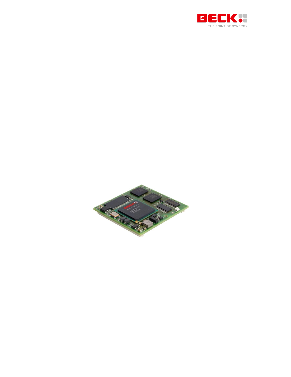
IPC@CHIP SC2x3
Hardware Manual V1.02 [01.03.09]
©2000-2009 BECK IPC GmbH Page 1
Hardware Manual
IPC@CHIP Embedded Controller Family
SC2x3
MPC5200
High Performance, 32-Bit Embedded Processor
Computer on Module (CoM) with Flash, RAM, Watchdog
Order No. IPC@CHIP
Embedded Controller SC243:
563963
Embedded Controller SC243-IEC:
Page 2

IPC@CHIP SC2x3
Hardware Manual V1.02 [01.03.09]
©2000-2009 BECK IPC GmbH Page 2
Copyright & Trademark
IPC@CHIP® is a registered trademark of Beck IPC. Ethernet is a
registered trademark of Xerox Corporation. All other product names,
company names, logos or other designations mentioned herein are
trademarks of their respective owners.
Freescale™ is a trademark of Freescale Semiconductor,
Inc.
Ethernet is a registered trademark of Xerox Corporation.
SPI is a trademark of Motorola, Inc.
No part of this guide may be reproduced or transmitted in any form for
any purpose other than the purchaser's personal use, without the express
written permission of Beck IPC.
Beck IPC GmbH
Grüninger Weg 24
35415 Pohlheim-Garbenteich / Germany
Phone: +49 6404 695-0
Fax: +49 6404 695-500
Technical Support
Page 3

IPC@CHIP SC2x3
Hardware Manual V1.02 [01.03.09]
©2000-2009 BECK IPC GmbH Page 3
Table of Contents
1 Overview .................................................................................................................... 6
2 Features ..................................................................................................................... 7
3 Block Diagram ............................................................................................................ 8
4 Pin Description ........................................................................................................... 9
4.1 Pin Configuration .......................................................................................................................... 9
4.2 Address-/Data Bus ...................................................................................................................... 10
4.3 Local Plus Bus ............................................................................................................................ 11
4.4 ATA Interface .............................................................................................................................. 11
4.5 USB1 – UART4+5 Interface ....................................................................................................... 12
4.6 PSC1 – UART1 ........................................................................................................................... 13
4.7 PSC2 – UART2 + CAN ............................................................................................................... 14
4.8 PSC3 – UART3/SPI .................................................................................................................... 15
4.9 PSC6 – UART6 ........................................................................................................................... 17
4.10 I²C Bus ........................................................................................................................................ 17
4.11 MII Interface ................................................................................................................................ 18
4.12 Timers ......................................................................................................................................... 18
4.13 Reset signals .............................................................................................................................. 18
4.14 COP/JTAG-Interface ................................................................................................................... 19
4.15 Interrupts ..................................................................................................................................... 19
4.16 Power .......................................................................................................................................... 20
4.17 Programmable I/O Pins .............................................................................................................. 22
5 Mutal Exclusive Functions ........................................................................................ 23
5.1 Mutal Exclusive Functions for USB1 .......................................................................................... 23
5.2 Mutal Exclusive Functions for PSC1 .......................................................................................... 23
5.3 Mutal Exclusive Functions for PSC2 .......................................................................................... 23
5.4 Mutal Exclusive Functions for PSC3 .......................................................................................... 24
5.5 Mutal Exclusive Functions for PSC6 .......................................................................................... 24
5.6 Mutal Exclusive Functions for I2C .............................................................................................. 24
5.7 Mutal Exclusive Functions for TIMER ......................................................................................... 24
5.8 Mutal Exclusive Functions for Local Plus Bus ............................................................................ 24
6 Functional Description .............................................................................................. 25
6.1 Local Plus Bus ............................................................................................................................ 25
6.1.1 Features ................................................................................................................................................ 25
6.1.2 Interface ................................................................................................................................................. 25
6.1.3 External Local Plus Bus Signals ............................................................................................................ 26
6.1.4 Local Plus Bus Address / Data Pin Assignments ................................................................................... 27
6.2 Programmable Serial Controllers ............................................................................................... 28
6.2.1 UARTs ................................................................................................................................................... 28
6.2.2 Usage of PIO0..PIO3 in consideration of UART1 (Bootloader interface) ................................ ............. 29
6.2.3 I²C .......................................................................................................................................................... 30
6.2.4 USB ....................................................................................................................................................... 31
6.2.5 SPI ......................................................................................................................................................... 31
6.2.6 CAN ....................................................................................................................................................... 32
6.3 Timers ......................................................................................................................................... 33
6.4 MII Interface ................................................................................................................................ 33
6.5 Reset ........................................................................................................................................... 33
Page 4

IPC@CHIP SC2x3
Hardware Manual V1.02 [01.03.09]
©2000-2009 BECK IPC GmbH Page 4
7 System interrupts ...................................................................................................... 34
7.1 Watchdog .................................................................................................................................... 34
8 Characteristics .......................................................................................................... 35
8.1 Absolute Maximum Ratings ........................................................................................................ 35
8.2 Recommended Operating Ranges ............................................................................................. 35
8.2.1 Voltage and Temperature ...................................................................................................................... 35
8.2.2 Supply Current ....................................................................................................................................... 35
8.2.3 Inputs ..................................................................................................................................................... 36
8.2.4 Outputs .................................................................................................................................................. 36
8.3 AC Characteristics ...................................................................................................................... 37
8.3.1 Muxed Mode .......................................................................................................................................... 37
8.3.2 Non-Muxed Mode .................................................................................................................................. 38
9 Package Information ................................................................................................. 40
9.1 Dimensions ................................................................................................................................. 40
9.2 SC2x3 Connector ....................................................................................................................... 40
10 Custom series programming of SC2x3 .................................................................. 41
11 History ................................................................................................................... 42
Page 5

IPC@CHIP SC2x3
Hardware Manual V1.02 [01.03.09]
©2000-2009 BECK IPC GmbH Page 5
Figures
Figure 3-1: Block Diagram ............................................................................................................................................... 8
Figure 4-1: Pin Configuration Looking through Top of Package ...................................................................................... 9
Figure 6-1: Internal block diagram of PIO0..PIO3 and UART1 ...................................................................................... 29
Figure 8-1: Timing Diagram – MUXed Mode ................................................................................................................. 37
Figure 8-2: Timing Diagram–MUXed Mode ................................................................................................................... 38
Figure 8-3: Timing Diagram–Non-MUXed Mode ........................................................................................................... 39
Figure 9-1: Package Dimensions. Top view through the conductor board. ................................................................... 40
Tables
Table 4-1: Pin Description of Local Plus Bus control signals ......................................................................................... 11
Table 4-2: Pin Description of ATA control signals ......................................................................................................... 11
Table 4-3: Pin Description of USB1 - UART4+5 Interface ............................................................................................. 13
Table 4-4: Pin Description of Programmable Serial Controller 1 ................................................................................... 13
Table 4-5: Pin Description of Programmable Serial Controller 2 ................................................................................... 14
Table 4-6: Pin Description of Programmable Serial Controller 3 ................................................................................... 16
Table 4-7: Pin Description of Programmable Serial Controller 6 ................................................................................... 17
Table 4-8: Pin Description of I²C Bus ............................................................................................................................ 17
Table 4-9: Pin Description of MII ................................................................................................................................... 18
Table 4-10: Pin Description of Timers ........................................................................................................................... 18
Table 4-11: Pin Description of Reset signals ................................................................................................................. 18
Table 4-12: Pin Description of COP/JTAG-Interface ..................................................................................................... 19
Table 4-13: Pin Description of Power Pins .................................................................................................................... 21
Table 4-14: List of PIO sharing designations ................................................................................................................. 22
Table 6-1: Provided CAN baud rates ............................................................................................................................. 32
Table 8-1: Absolute Maximum Ratings .......................................................................................................................... 35
Table 8-2: Recommended Operating Ranges ............................................................................................................... 35
Table 8-3: Supply Current ............................................................................................................................................. 35
Table 8-4: Inputs ........................................................................................................................................................... 36
Table 8-5: Outputs ......................................................................................................................................................... 36
Page 6

IPC@CHIP SC2x3
Hardware Manual V1.02 [01.03.09]
©2000-2009 BECK IPC GmbH Page 6
1 Overview
The IPC@CHIP® SC2x3 family is a combination of hardware and software including the preinstalled real time
operating system, TCP/IP stack, Web server, FTP server, Telnet server, enable designers to reduce the size,
power consumption, and cost of embedded systems, while increasing reliability, functionality, performance and
time to market.
The IPC@CHIP® SC2x3 family of Computer on Modules are embedded processors built on Power
Architecture™ technology and are specially designed for demanding control, communication and HMI tasks.
The Freescale power processor offers 760 MIPS processing performance and a high-speed Floating Point Unit
– ideal for fast data communication or complex control tasks for example in the field of motion control.
As an option it can also be used in combination with an IEC61131-3 CoDeSys Run Time System.
IPC@CHIP
RAM
FLASH
CoDeSys license included
SC243
64 MByte
32 MByte
no
SC243-IEC
64 MByte
32 MByte
yes
Page 7

IPC@CHIP SC2x3
Hardware Manual V1.02 [01.03.09]
©2000-2009 BECK IPC GmbH Page 7
2 Features
32-Bit Freescale PowerPC Processor MPC5200B
Up to 400MHz with MPC603e Processor Core
Double Precision Floating Point Unit (FPU)
Instruction and Data Memory Management Unit (MMU)
16K Instruction and 16K Data Caches
BestComm Intelligent DMA I/O Controller
Memory
SDRAM: 16MB / 64 MB; 32Bit data length
Flash: 16MB / 32MB Flash; 32Bit data length
SRAM: 512kByte; can be supplied from battery on basis board
Parallel Interfaces
10/100 Ethernet MAC
ATA/IDE Interface
Local Plus interface
6 x Programmable Serial Controllers usable as
2 x USB 1.1 Host
6 x RS232/422/485 RTS/CTS/DCD
5 x Serial Peripheral Interface (SPI)
2 x I²C
2 x CAN 2.0B
Power Supply
Single Power Supply 3.3V
Switch-Mode DC/DC Converter on the Module (3.3V on 1.5V)
Linear DC/DC Converter on the Module (3.3V on1.8V)
1,5V / 1,8V / 3,3V Supervisory Circuit
Watchdog and power-on Reset Logic
GPIOs
40 Programmable Input/Output (PIO) Pins
Dimension
56 mm x 60 mm
240 Pin Board-to-Board connector system
Page 8
IPC@CHIP SC2x3
Hardware Manual V1.02 [01.03.09]
©2000-2009 BECK IPC GmbH Page 8
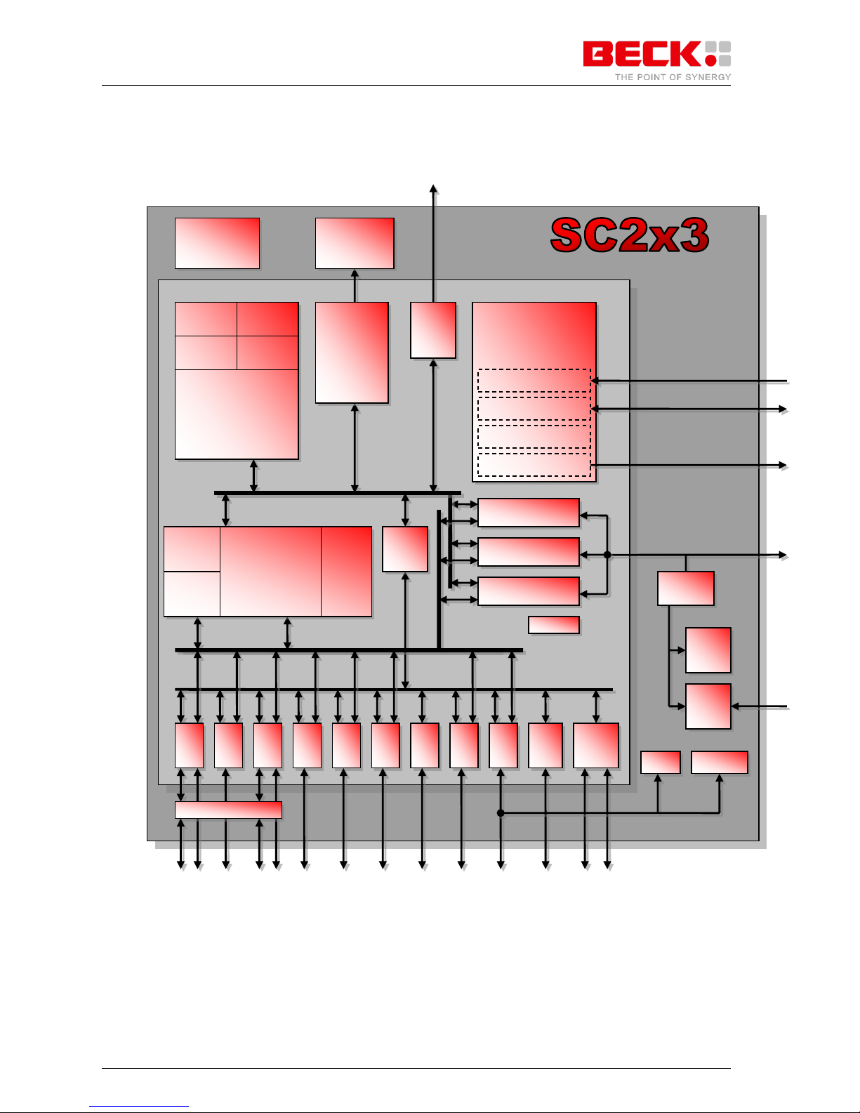
3 Block Diagram
Figure 3-1: Block Diagram
Embedded
PowerPC 603e
Core
With double
precision FPU
16K
lCache
32 Entry
MMU
16K
DCache
32 Entry
MMU
Systems Integration
Unit
Interrupt Control
System Functions
Real Time Clock
Chip Selects
JTAG
XL Bus
SDRAM
Memory
Controller
USB
(two)
BestComm
Intelligent DMA
Unit
Clock/Reset
Generation
GPIO
16K
SRAM
IPBI
PSC1
PSC2
PSC3
PSC4
PSC5
PSC6
SPI
10/100
BaseT
I²C
(two)
J1850
CAN 2.0
A/B
(two)
PCI Controller
ROM/SRAM
ATA/IDE Host
Controller
SDRAM
V24 Transceiver
Power
Supervisory
Circuit
Driver/
Buffer
Flash
SRAM
LM75
E²PROM
Page 9
IPC@CHIP SC2x3
Hardware Manual V1.02 [01.03.09]
©2000-2009 BECK IPC GmbH Page 9
4 Pin Description
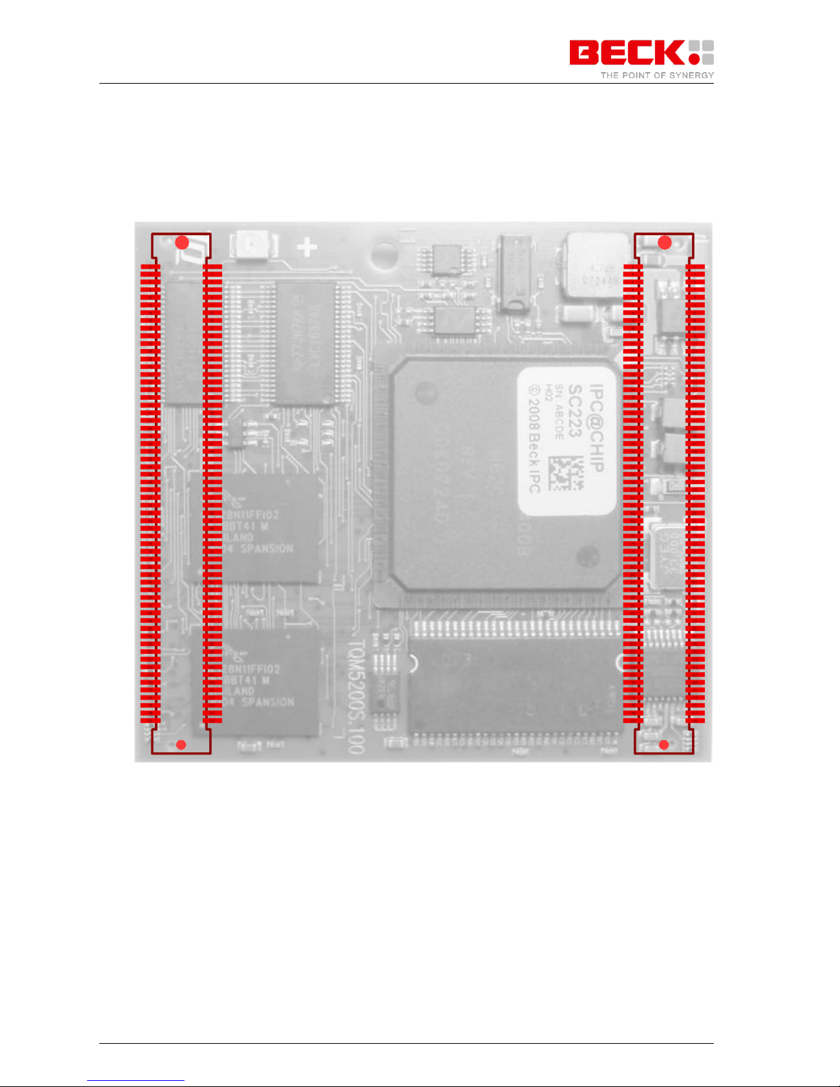
4.1 Pin Configuration
Figure 4-1: Pin Configuration Looking through Top of Package
X3
X1
Page 10

IPC@CHIP SC2x3
Hardware Manual V1.02 [01.03.09]
©2000-2009 BECK IPC GmbH Page 10
4.2 Address-/Data Bus
Pin Name
Pin
Con
Type
Description
EXT_AD[0]
92
X1
I/O[16mA]
Address / Data bus
EXT_AD[1]
89
X1
I/O[16mA]
Address / Data bus
EXT_AD[2]
88
X1
I/O[16mA]
Address / Data bus
EXT_AD[3]
87
X1
I/O[16mA]
Address / Data bus
EXT_AD[4]
86
X1
I/O[16mA]
Address / Data bus
EXT_AD[5]
83
X1
I/O[16mA]
Address / Data bus
EXT_AD[6]
84
X1
I/O[16mA]
Address / Data bus
EXT_AD[7]
81
X1
I/O[16mA]
Address / Data bus
EXT_AD[8]
80
X1
I/O[16mA]
Address / Data bus
EXT_AD[9]
79
X1
I/O[16mA]
Address / Data bus
EXT_AD[10]
78
X1
I/O[16mA]
Address / Data bus
EXT_AD[11]
77
X1
I/O[16mA]
Address / Data bus
EXT_AD[12]
76
X1
I/O[16mA]
Address / Data bus
EXT_AD[13]
75
X1
I/O[16mA]
Address / Data bus
EXT_AD[14]
72
X1
I/O[16mA]
Address / Data bus
EXT_AD[15]
71
X1
I/O[16mA]
Address / Data bus
EXT_AD[16]
70
X1
I/O[16mA]
Address / Data bus
EXT_AD[17]
69
X1
I/O[16mA]
Address / Data bus
EXT_AD[18]
68
X1
I/O[16mA]
Address / Data bus
EXT_AD[19]
67
X1
I/O[16mA]
Address / Data bus
EXT_AD[20]
64
X1
I/O[16mA]
Address / Data bus
EXT_AD[21]
65
X1
I/O[16mA]
Address / Data bus
EXT_AD[22]
62
X1
I/O[16mA]
Address / Data bus
EXT_AD[23]
63
X1
I/O[16mA]
Address / Data bus
EXT_AD[24]
60
X1
I/O[16mA]
Address / Data bus
EXT_AD[25]
59
X1
I/O[16mA]
Address / Data bus
EXT_AD[26]
56
X1
I/O[16mA]
Address / Data bus
EXT_AD[27]
57
X1
I/O[16mA]
Address / Data bus
EXT_AD[28]
TSIZ[2]
54
X1
I/O[16mA]
I/O[16mA]
Address / Data bus
Transfer Size 2 indicates the size of the transaction in
muxed mode
EXT_AD[29]
TSIZ[1]
55
X1
I/O[16mA]
I/O[16mA]
Address / Data bus
Transfer Size 1 indicates the size of the transaction in
muxed mode.
EXT_AD[30]
TSIZ[0]
52
X1
I/O[16mA]
I/O[16mA]
Address / Data bus
Transfer Size 0 indicates the size of the transaction in
muxed mode.
EXT_AD[31]
53
X1
I/O[16mA]
Address / Data bus (bi-directional when used as data; bit
31=msb).
GPIO7
TSIZ[1]
PIO31
84
X3
I/O[8mA]
Transfer Size 1 indicates the size of the transaction in
non-muxed mode or PIO31.
TEST_SEL_1
TSIZ[2]
12
X3
OUT[8mA]
Transfer Size 2 indicates the size of the transaction in
non-muxed mode.
Page 11
IPC@CHIP SC2x3
Hardware Manual V1.02 [01.03.09]
©2000-2009 BECK IPC GmbH Page 11
4.3 Local Plus Bus
Pin Name
Pin
Con
Type
Description
LP_CS0#
116
X1
OUT[8mA]
Reserved. Do not connect. (internal 100kOhm pullup)
LP_CS1#
113
X1
OUT[8mA]
Local Plus Bus Chip Select (internal 100kOhm pullup)
LP_CS2#
112
X1
OUT[8mA]
Reserved. Do not connect. (internal 100kOhm pullup)
LP_CS3#
111
X1
OUT[8mA]
Local Plus Bus Chip Select (internal 100kOhm pullup)
LP_CS4#
110
X1
OUT[8mA]
ATA Chip Select CS0# (internal 100kOhm pullup)
LP_CS5#
108
X1
OUT[8mA]
ATA Chip Select CS1# (internal 100kOhm pullup)
LP_RW
91
X1
OUT[8mA]
Read/Write control signal, 1 = Read, 0 = Write
LP_ALE#
93
X1
OUT[8mA]
Local Plus Bus Address Latch Enable
LP_TS#
94
X1
OUT[8mA]
Local Plus Bus Transfer Start
LP_ACK#
95
X1
IN/
OUT[8mA]
Local Plus Bus External Acknowledge input (Open
Drain with internal pullup)
LP_OE#
96
X1
OUT[8mA]
Local Plus Bus Output Enable
Table 4-1: Pin Description of Local Plus Bus control signals
4.4 ATA Interface
Pin Name
Pin
Con
Type
Description
ATA_IOR#
100
X1
OUT[8mA]
ATA I/O Read output (Active Low)
This pin indicates a read transaction on ATA Interface
ATA_IOW#
101
X1
OUT[8mA]
ATA I/O Write output (Active Low)
This pin indicates a write transaction on ATA Interface
ATA_ISOLATION
99
X1
OUT[8mA]
ATA Isolation (Active High)
This pin is an active high signal to control external ATA
transceiver devices and to isolate the ATA bus from the
shared Local Plus bus.
ATA_INTRQ
102
X1
IN
ATA Interrupt (Active High with internal 10kOhm
pulldown)
This pin is the external ATA interrupt request.
ATA_DACK#
104
X1
IN
ATA DMA Acknowledge (Active Low)
ATA_IOCHRDY
103
X1
IN
ATA I/O Channel Ready (Active High with internal
10kOhm pullup)
This pin is used to extend ATA bus accesses
ATA_DRQ
105
X1
IN
ATA DMA Request (Active High with internal 10kOhm
pulldown)
Table 4-2: Pin Description of ATA control signals
Page 12

IPC@CHIP SC2x3
Hardware Manual V1.02 [01.03.09]
©2000-2009 BECK IPC GmbH Page 12
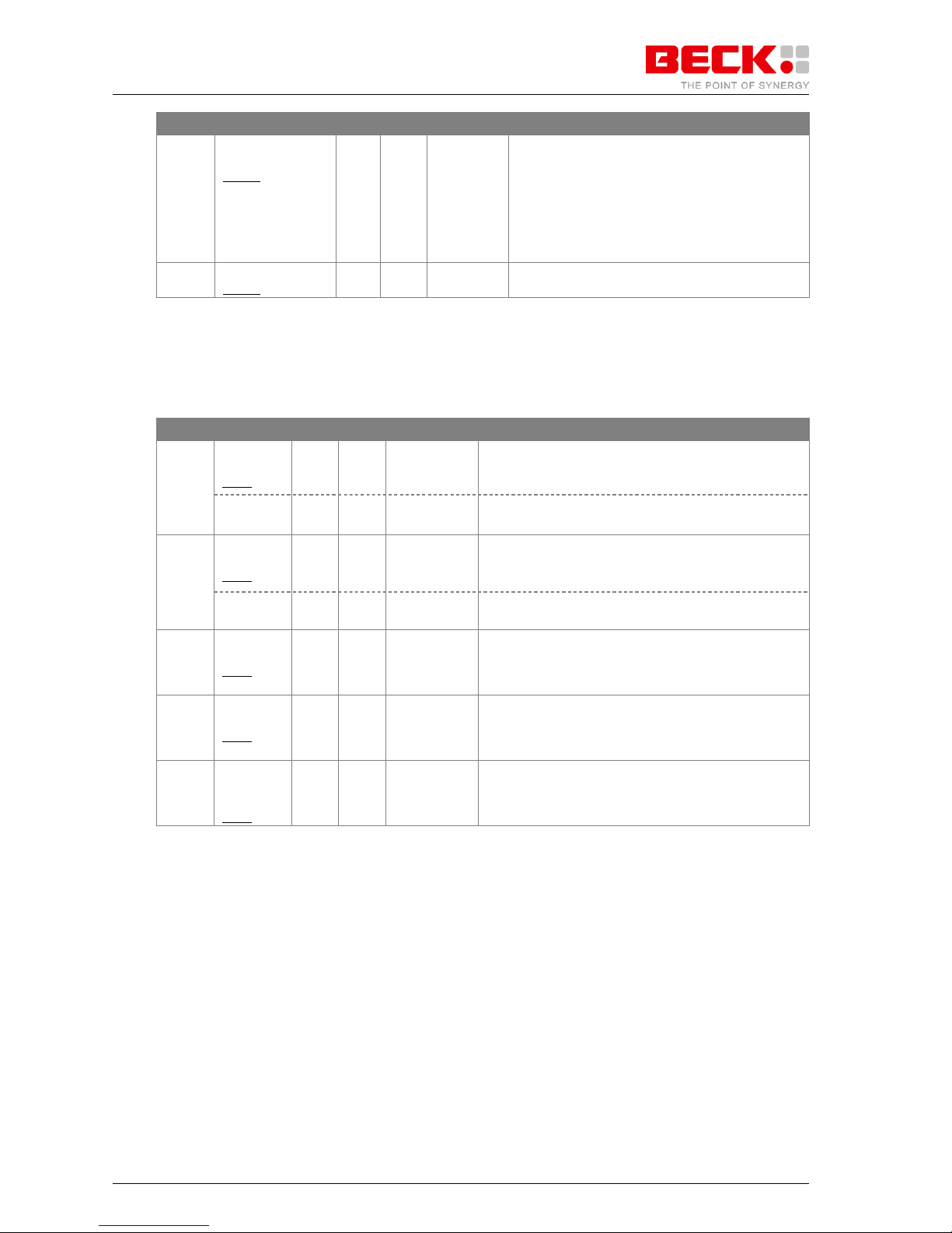
4.5 USB1 – UART4+5 Interface
#USB1
Pin Name
Pin
Con
Type
Description
0
USB1_OE
PIO24
20
X3
OUT[4mA]
I/O[4mA]
USB 1 Output Enable (Active Low)
This pin is used to enable the transceiver to
transmit data on the bus or as PIO24.
1
USB1_TXN
19
X3
OUT[4mA]
USB 1 Transmit Negative
This pin is the negative output to the differential
driver.
RTS4
OUT[4mA]
Ready to Send 4 Out
This pin provides the Ready to Send output for
serial port 4. It provides the handshaking output
for serial port 4.
2
USB1_TXP
22
X3
OUT[4mA]
USB 1 Transmit Positive
This pin is the positive output to the differential
driver.
TXD4
OUT[4mA]
Transmit Data 4 Out
This pin provides serial Transmit data to the
system from serial port 4.
3
USB1_RXD
21
X3
IN
USB 1 Receive Data
This pin is the data input from the differential
driver.
RXD4
IN
Receive Data 4 In
This pin provides serial Receive Data from the
system to serial port 4.
4
USB1_RXP
24
X3
IN
USB 1 Receive Positive
This pin is used to detect single ended zero
(/SEO), error conditions, and interconnected
speed.
CTS4
IN
Clear to Send 4 In
This pin provides the Clear to Send input for
serial port 4. It provides the handshaking input
for serial port 4.
5
USB1_RXN
23
X3
IN
USB 1 Receive Negative
This pin is used to detect single ended zero
(/SEO), error conditions, and interconnected
speed.
RXD5
IN
Receive Data 5 In
This pin provides serial Receive Data from the
system to serial port 5.
6
USB1_PRTPWR
PIO25
28
X3
OUT[4mA]
I/O[4mA]
USB 1 Port Power (Active Low)
This pin can be used to enable the USB port
power output or as PIO25.
TXD5
OUT[4mA]
Transmit Data 5 Out
This pin provides serial Transmit data to the
system from serial port 5.
7
USB1_SPEED
PIO26
27
X3
OUT[4mA]
I/O[4mA]
USB 1 Speed (Active High)
This pin controls the Edge Rate Control; 1=full
speed, 0=low speed or as PIO26.
RTS5
OUT[4mA]
Ready to Send 5 Out
This pin provides the Ready to Send output for
serial port 5. It provides the handshaking output
for serial port 5.
Page 13
IPC@CHIP SC2x3
Hardware Manual V1.02 [01.03.09]
©2000-2009 BECK IPC GmbH Page 13
#USB1
Pin Name
Pin
Con
Type
Description
8
USB1_SUSPEND
PIO27
30
X3
OUT[4mA]
I/O[4mA]
USB 1 Suspend (Active High)
This pin enables a low-power state while the
USB bus is inactive or can be used as PIO27.
CTS5
IN
Clear to Send 5 In
This pin provides the Clear to Send input for
serial port 5. It provides the handshaking input
for serial port 5.
9
USB1_OVRCNT
PIO28
29
X3
IN
I/O[4mA]
USB 1 Overcurrent Detection
This pin can also be used as PIO28.
Table 4-3: Pin Description of USB1 - UART4+5 Interface
4.6 PSC1 – UART1
#PSC1
Pin Name
Pin
Con
Type
Description
0
TXD1
PIO0
65
X3
OUT[4mA]
I/O[4mA]
Transmit Data 1 Out
This pin provides serial Transmit data to the system
from serial port 1 or can be used as PIO0
TXD1
72
X3
OUT[RS232]
Transmit Data 1 Out
This pin provides the signal TXD1 using RS232 level.
1
RXD1
PIO1
63
X3
IN
I/O[4mA]
Receive Data 1 In
This pin provides serial Receive Data from the system
to serial port 1 or can be used as PIO1
RXD1
71
X3
IN[RS232]
Receive Data 1 In
This pin provides the signal RXD1 using RS232 level.
2
RTS1
PIO2
64
X3
OUT[4mA]
I/O[4mA]
Ready to Send 1 Out
This pin provides the Ready to Send output for serial
port 1. It provides the handshaking output for serial
port 1 or can be used as PIO2.
3
CTS1
PIO3
59
X3
IN
I/O[4mA]
Clear to Send 1 In
This pin provides the Clear to Send input for serial
port 1. It provides the handshaking input for serial port
1 or can be used as PIO3.
4
DCD1
PIO4
62
X3
IN
I/O[4mA]
Data Carrier Detect 1 Input
In the enhanced UART mode this signal must be
assert during the data transmission.
This pin can slo be used as PIO4.
Table 4-4: Pin Description of Programmable Serial Controller 1
Page 14

IPC@CHIP SC2x3
Hardware Manual V1.02 [01.03.09]
©2000-2009 BECK IPC GmbH Page 14
4.7 PSC2 – UART2 + CAN
#PSC2
Pin Name
Pin
Con
Type
Description
0
TXD2
60
X3
OUT[4mA]
Transmit Data 2 Out
This pin provides serial Transmit data to the system
from serial port 2.
CAN1TXD
OUT[4mA]
CAN Transmit 1
This pin can be used as CAN controller 1 Transmit.
PIO5
I/O[4mA]
This pin can also be used as PIO5.
1
RXD2
57
X3
IN
Receive Data 2 In
This pin provides serial Receive Data from the system
to serial port 2.
CAN1RXD
IN
CAN Receiver 1
This pin can be used as CAN controller 1 Receive.
PIO6
I/O[4mA]
This pin can also be used as PIO6.
2
RTS2
56
X3
OUT[4mA]
Ready to send 2 Out
This pin provides the Ready to Send output for serial
port 2. It provides the handshaking output for serial
port 2.
CAN2TXD
OUT[4mA]
CAN Transmit 2
This pin can be used as CAN controller 2 Transmit.
PIO7
I/O[4mA]
This pin can also be used as PIO7.
3
CTS2
55
X3
IN
Clear to Send 2 In
This pin provides the Clear to Send input for serial
port 2. It provides the handshaking input for serial
port 2.
CAN2RXD
IN
CAN Receiver 2
This pin can be used as CAN controller 2 Receive.
PIO8
I/O[4mA]
This pin can also be used as PIO8.
4
DCD2
54
X3
IN
Data Carrier Detect 2 Input
In the enhanced UART mode this signal must be
assert during the data transmission.
PIO9
I/O[4mA]
This pin can also be used as PIO9.
Table 4-5: Pin Description of Programmable Serial Controller 2
Page 15

IPC@CHIP SC2x3
Hardware Manual V1.02 [01.03.09]
©2000-2009 BECK IPC GmbH Page 15
4.8 PSC3 – UART3/SPI
#PSC3
Pin Name
Pin
Con
Type
Description
0
TXD3
53
X3
OUT[4mA]
Transmit Data 3 Out
This pin provides serial Transmit data to
the system from serial port 3.
USB2_OE
OUT[4mA]
USB 2 Output Enable (Active Low)
This pin is used to enable the transceiver to
transmit data on the bus.
PIO10
I/O[4mA]
This pin can also be used as PIO10.
TXD3
76
X3
OUT[RS232]
Transmit Data 1 Out
This pin provides the signal TXD3 using
RS232 level.
1
RXD3
51
X3
IN
Receive Data 3 In
This pin provides serial Receive Data from
the system to serial port 3.
USB2_TXN
OUT[4mA]
USB 2 Transmit Negative
This pin is the negative output to the
differential driver.
PIO11
I/O[4mA]
This pin can also be used as PIO11.
RXD3
75
X3
IN[RS232]
Receive Data 1 In
This pin provides the signal RXD1 using
RS232 level.
2
RTS3
52
X3
OUT[4mA]
Ready to send 3 Out
This pin provides the Ready to Send output
for serial port 3. It provides the
handshaking output for serial port 3.
USB2_TXP
OUT[4mA]
USB 2 Transmit Positive
This pin is the positive output to the
differential driver.
PIO12
I/O[4mA]
This pin can also be used as PIO12.
3
CTS3
47
X3
IN
Clear to Send 3 In
This pin provides the Clear to Send input
for serial port 3. It provides the
handshaking input for serial port 3.
USB2_RXD
IN
USB 1 Receive Data
This pin is the data input from the
differential driver.
PIO13
I/O[4mA]
This pin can also be used as PIO13.
4
DCD3
48
X3
IN
Data Carrier Detect 3 Input
In the enhanced UART mode this signal
must be assert during the data
transmission.
USB2_RXP
IN
USB 2 Receive Positive
This pin is used to detect single ended
zero, error conditions, and interconnected
speed.
LP_CS6#
OUT[8mA]
Local Plus Bus Chip Select shared with
PSC3
PIO14
I/O[8mA]
This pin can also be used as PIO14.
Page 16

IPC@CHIP SC2x3
Hardware Manual V1.02 [01.03.09]
©2000-2009 BECK IPC GmbH Page 16
5
USB2_RXN
45
X3
IN
USB 2 Receive Negative
This pin is used to detect single ended zero
error conditions, and interconnected speed.
LP_CS7#
OUT[8mA]
Local Plus Bus Chip Select shared with
PSC3
PIO15
I/O[8mA]
This pin can also be used as PIO15.
6
MOSI
46
X3
OUT[4mA]
SPI Master Data Out/Slave Data In
USB2_PRTPWR
OUT[4mA]
USB 2 Port Power (Active Low)
This pin can be used to enable the USB
port power output.
PIO16
I/O[4mA]
This pin can also be used as PIO16.
7
MISO
43
X3
IN
SPI Master Data In/Slave Data Out
USB2_SPEED
OUT[4mA]
USB 2 Speed (Active High)
This pin controls the Edge Rate Control.
1=full speed, 0=low speed.
PIO17
I/O[4mA]
This pin can also be used as PIO17.
8
SS
44
X3
OUT[4mA]
SPI Slave Select
USB2_SUSPEND
OUT[4mA]
USB 2 Suspend (Active High)
This pin enables a low-power state while
the USB bus is inactive.
PIO18
I/O[4mA]
This pin can also be used as PIO18.
9
SCK
41
X3
OUT[4mA]
SPI Serial Clock
USB2_OVRCNT
IN
USB 2 Overcurrent Detection
PIO19
I/O[4mA]
This pin can also be used as PIO19.
Table 4-6: Pin Description of Programmable Serial Controller 3
Page 17
IPC@CHIP SC2x3
Hardware Manual V1.02 [01.03.09]
©2000-2009 BECK IPC GmbH Page 17
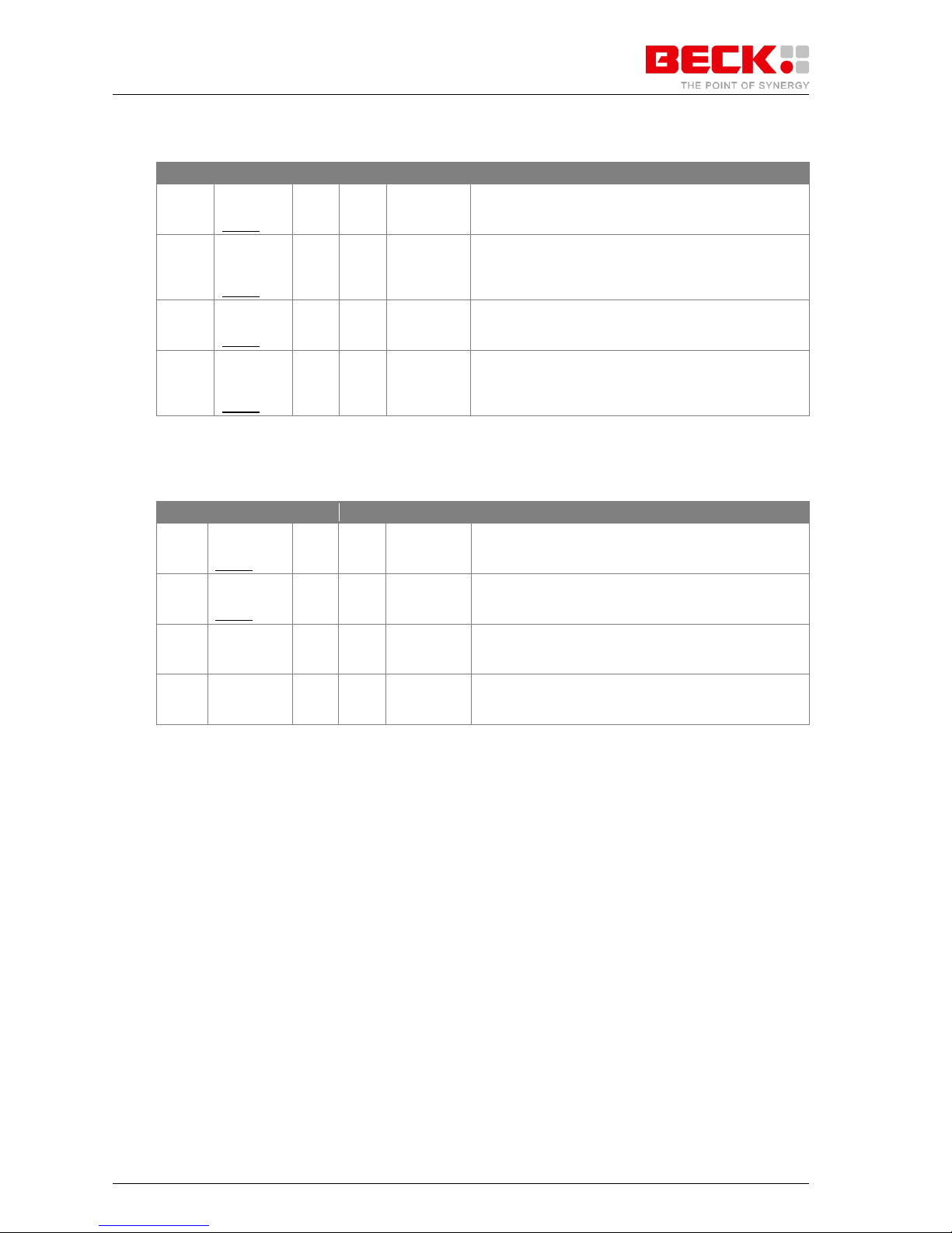
4.9 PSC6 – UART6
#PSC6
Pin Name
Pin
Con
Type
Description
0
RXD6
PIO20
70
X3
IN
I/O[4mA]
Receive Data 6 In
This pin provides serial Receive Data from the system
to serial port 6 or can be used as PIO20.
1
CTS6
PIO21
69
X3
IN
I/O[4mA]
Clear to Send 6 In
This pin provides the Clear to Send input for serial port
6. It provides the handshaking input for serial port 6 or
can be used as PIO21.
2
TXD6
PIO22
68
X3
OUT[4mA]
I/O[4mA]
Transmit Data 6 Out
This pin provides serial Transmit data to the system
from serial port 6 or can be used as PIO22.
3
RTS6
PIO23
67
X3
OUT[4mA]
I/O[4mA]
Ready to send 6 Out
This pin provides the Ready to Send output for serial
port 6. It provides the handshaking output for serial
port 6 or can be used as PIO23.
Table 4-7: Pin Description of Programmable Serial Controller 6
4.10 I²C Bus
#I2C
Pin Name
Pin
Con
Type
Description
0
I2CCLK1
PIO29
80
X3
I/O[4mA]
I/O[4mA]
I²C bus 1 Clock (Schmitt Input)
This pin can be used with the I²C block as the I2CCLK
or as PIO29.
1
I2CDTA1
PIO30
79
X3
I/O[4mA]
I/O[4mA]
I²C bus 1 Data (Schmitt Input)
This pin can be used with the I²C block as the I2CDTA
or as PIO30.
2
I2CCLK2
78
X3
OUT[4mA]
I²C bus 2 Clock (Schmitt Input with internal 10kOhm
pullup)
This pin can be used with the I²C block as the I2CCLK.
3
I2CDTA2
77
X3
I/O[4mA]
I²C bus 2 Data (Schmitt Input with internal 10kOhm
pullup)
This pin can be used with the I²C block as the I2CDTA.
Table 4-8: Pin Description of I²C Bus
Page 18
IPC@CHIP SC2x3
Hardware Manual V1.02 [01.03.09]
©2000-2009 BECK IPC GmbH Page 18
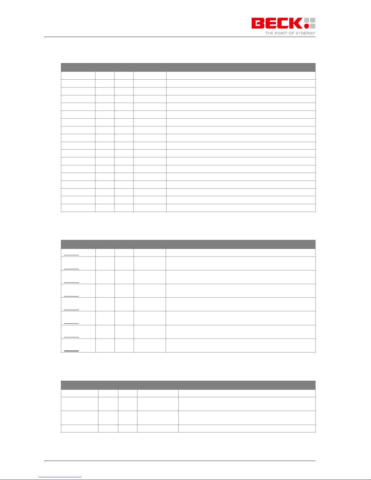
4.11 MII Interface
Pin Name
Pin
Con
Type
Description
MDIO
15
X1
I/O [4mA]
Ethernet MII 1 Management Data
MDC
16
X1
OUT [4mA]
Ethernet MII 1 Clock Out
TXCLK
9
X1
IN
Ethernet Transmit Clock
TXEN
24
X1
OUT [4mA]
Ethernet Transmit Enable (internal 100kOhm Pullup)
TXER
17
X1
OUT [4mA]
Ethernet Transmit Error
TXD[3]
20
X1
OUT [4mA]
Ethernet Transmit Data Bus Bit [3]
TXD[2]
19
X1
OUT [4mA]
Ethernet Transmit Data Bus Bit [2]
TXD[1]
22
X1
OUT [4mA]
Ethernet Transmit Data Bus Bit [1]
TXD[0]
21
X1
OUT [4mA]
Ethernet Transmit Data Bus Bit [0]
RXCLK
11
X1
IN
Ethernet Receive Clock
RXDV
14
X1
IN
Ethernet Receive Data Valid
RXER
4
X1
IN
Ethernet Receive Error
RXD[3]
5
X1
IN
Ethernet Receive Data Bus Bit [3]
RXD[2]
6
X1
IN
Ethernet Receive Data Bus Bit [2]
RXD[1]
7
X1
IN
Ethernet Receive Data Bus Bit [1]
RXD[0]
8
X1
IN
Ethernet Receive Data Bus Bit [0]
RXCRS
3
X1
IN
Ethernet Receive Carrier Sense
RXCOL
12
X1
IN
Ethernet Receive Collision
Table 4-9: Pin Description of MII
4.12 Timers
Pin Name
Pin
Con
Type
Description
PIO32
32
X3
I/O[4mA]
Internal TIMER0 can only be used as PIO32.
TIMER1
PIO33
31
X3
I/O[4mA]
I/O[4mA]
Timer 1
This pin can also be used as PIO33.
TIMER2
PIO34
36
X3
I/O[4mA]
I/O[4mA]
Timer 2
This pin can also be used as PIO34.
TIMER3
PIO35
33
X3
I/O[4mA]
I/O[4mA]
Timer 3
This pin can also be used as PIO35.
TIMER4
PIO36
38
X3
I/O[4mA]
I/O[4mA]
Timer 4
This pin can also be used as PIO36.
TIMER5
PIO37
35
X3
I/O[4mA]
I/O[4mA]
Timer 5
This pin can also be used as PIO37.
TIMER6
PIO38
40
X3
I/O[4mA]
I/O[4mA]
Timer 6
This pin can also be used as PIO38.
TIMER7
PIO39
39
X3
I/O[4mA]
I/O[4mA]
Timer 7
This pin can also be used as PIO39.
Table 4-10: Pin Description of Timers
4.13 Reset signals
Pin Name
Pin
Con
Type
Description
RESIN#
4
X3
IN
Reset In (Active Low, Schmitt Input, 5.6kOhm pullup)
HRESET#
3
X3
IN/OUT [8mA]
Hardware Reset (Active Low, Schmitt Trigger Input with
internal 10kOhm pullup)
SRESET#
6
X3
IN/OUT [8mA]
Software Reset (Active Low, Schmitt Trigger Input with
internal 10kOhm pullup)
PORRESET#
5
X3
OUT [4mA]
Power On Reset (Active Low)
Table 4-11: Pin Description of Reset signals
Page 19

IPC@CHIP SC2x3
Hardware Manual V1.02 [01.03.09]
©2000-2009 BECK IPC GmbH Page 19
4.14 COP/JTAG-Interface
Pin Name
Pin
Con
Type
Description
JTAG_TCK
14
X3
IN
JTAG Clock (Schmitt Trigger Input with internal 10kOhm
pullup)
The (non-reset) behavior of the active TAP and TLM state
machines is governed by the TMS value at the TCK rising
edge. TDI value is sampled at the TCK rising edge for all
shift operations. All TDO non-reset transitions (including
impedance) occur at the TCK falling edge. All shift register
capture operations occur at the TCK rising edge. All shift
register Update operations occur at the TCK falling edge.
JTAG_TDI
9
X3
IN
JTAG Data Input (with internal 10kOhm pullup)
Serial test data input can be routed to any IR or DR, as
determined by the state of the active TAP state machine and
the contents of the active IR. TDI is sampled at the TCK
rising edge while the active TAP state machine is in either
the Shift-IR or Shift-DR state.
JTAG_TDO
8
X3
OUT [8mA]
JTAG Data Output
TDO when connected to TDI (of another device), TDO
switches at the TCK falling edge. TDO is driven while the
TLM state machine is in the Shift-IR or Shift-DR states only;
it is tri-stated in all other TAP
states. Except, for the first half clock after exiting the shift
state, because of its falling edge timing.
JTAG_TMS
7
X3
IN
JTAG Mode Select (with internal 10kOhm pullup)
TAP state machine control, including TLM. The state of TMS
at rising edges of TCK uniquely determines the state
sequence of the TLM and the active TAP state machines.
Inactive TAPs ignore TMS completely.
JTAG_TRST#
11
X3
IN
JTAG Reset (Active Low with internal Pull-up)
When asserted, any on-going JTAG operation is immediately
aborted. All TAP state machines, including the TLM,
immediately enter the Test-Logic-Reset state. Other JTAG
input signals (TCK, TMS, and TDI) have no effect while
TRST is asserted. TDO is immediately tri-stated.
TEST_SEL_0
16
X3
IN TEST_SEL_1
12
X3
IN
internal 10kOhm pullup
Table 4-12: Pin Description of COP/JTAG-Interface
4.15 Interrupts
Pin Name
Pin
Con
Type
Description
IRQ0
30
X1
IN
Interrupt 0 (Active High with internal 100kOhm pullup)
This pin is the external interrupt 0 request.
IRQ1
27
X1
IN
Interrupt 1 (Active High with internal 100kOhm pullup)
This pin is the external interrupt 0 request.
IRQ2
28
X1
IN
Interrupt 2 (Active High with internal 100kOhm pulldown)
This pin is the external interrupt 0 request.
IRQ3
23
X1
IN
Interrupt 3 (Active High with internal 100kOhm pulldown)
This pin is the external interrupt 0 request.
Table 4-13: Pin Description of Interrupts
Page 20

IPC@CHIP SC2x3
Hardware Manual V1.02 [01.03.09]
©2000-2009 BECK IPC GmbH Page 20
4.16 Power
Pin Name
Pin
Con
Type
Description
VCC 1 X3
PWR
Power I/O: +3.3 volt power supply
VCC
13
X3
PWR
Power I/O: +3.3 volt power supply
VCC
25
X3
PWR
Power I/O: +3.3 volt power supply
VCC
37
X3
PWR
Power I/O: +3.3 volt power supply
VCC
49
X3
PWR
Power I/O: +3.3 volt power supply
VCC
61
X3
PWR
Power I/O: +3.3 volt power supply
VCC
73
X3
PWR
Power I/O: +3.3 volt power supply
VCC
85
X3
PWR
Power I/O: +3.3 volt power supply
VCC
97
X3
PWR
Power I/O: +3.3 volt power supply
VCC
109
X3
PWR
Power I/O: +3.3 volt power supply
VCC
119
X3
PWR
Power I/O: +3.3 volt power supply
GND 2 X3
PWR
Power VSS
GND
10
X3
PWR
Power VSS
GND
18
X3
PWR
Power VSS
GND
26
X3
PWR
Power VSS
GND
34
X3
PWR
Power VSS
GND
42
X3
PWR
Power VSS
GND
50
X3
PWR
Power VSS
GND
58
X3
PWR
Power VSS
GND
66
X3
PWR
Power VSS
GND
74
X3
PWR
Power VSS
GND
82
X3
PWR
Power VSS
GND
90
X3
PWR
Power VSS
GND
98
X3
PWR
Power VSS
GND
106
X3
PWR
Power VSS
GND
114
X3
PWR
Power VSS
GND
120
X3
PWR
Power VSS
VCC 1 X1
PWR
Power I/O: +3.3 volt power supply
VCC
13
X1
PWR
Power I/O: +3.3 volt power supply
VCC
25
X1
PWR
Power I/O: +3.3 volt power supply
VCC
37
X1
PWR
Power I/O: +3.3 volt power supply
VCC
49
X1
PWR
Power I/O: +3.3 volt power supply
VCC
61
X1
PWR
Power I/O: +3.3 volt power supply
VCC
73
X1
PWR
Power I/O: +3.3 volt power supply
VCC
85
X1
PWR
Power I/O: +3.3 volt power supply
VCC
97
X1
PWR
Power I/O: +3.3 volt power supply
VCC
109
X1
PWR
Power I/O: +3.3 volt power supply
VCC
119
X1
PWR
Power I/O: +3.3 volt power supply
GND 2 X1
PWR
Power VSS
GND
10
X1
PWR
Power VSS
GND
18
X1
PWR
Power VSS
GND
26
X1
PWR
Power VSS
GND
34
X1
PWR
Power VSS
GND
42
X1
PWR
Power VSS
GND
50
X1
PWR
Power VSS
GND
58
X1
PWR
Power VSS
GND
66
X1
PWR
Power VSS
Page 21

IPC@CHIP SC2x3
Hardware Manual V1.02 [01.03.09]
©2000-2009 BECK IPC GmbH Page 21
Pin Name
Pin
Con
Type
Description
GND
74
X1
PWR
Power VSS
GND
82
X1
PWR
Power VSS
GND
90
X1
PWR
Power VSS
GND
98
X1
PWR
Power VSS
GND
106
X1
PWR
Power VSS
GND
114
X1
PWR
Power VSS
GND
120
X1
PWR
Power VSS
Table 4-14: Pin Description of Power Pins
Page 22
IPC@CHIP SC2x3
Hardware Manual V1.02 [01.03.09]
©2000-2009 BECK IPC GmbH Page 22
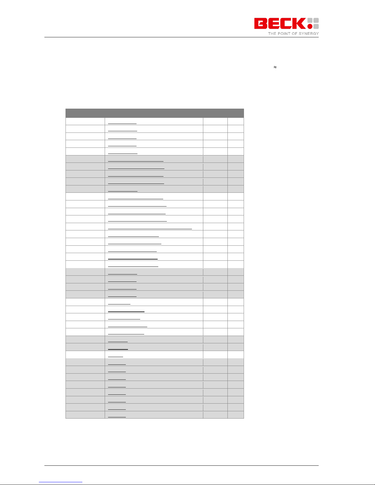
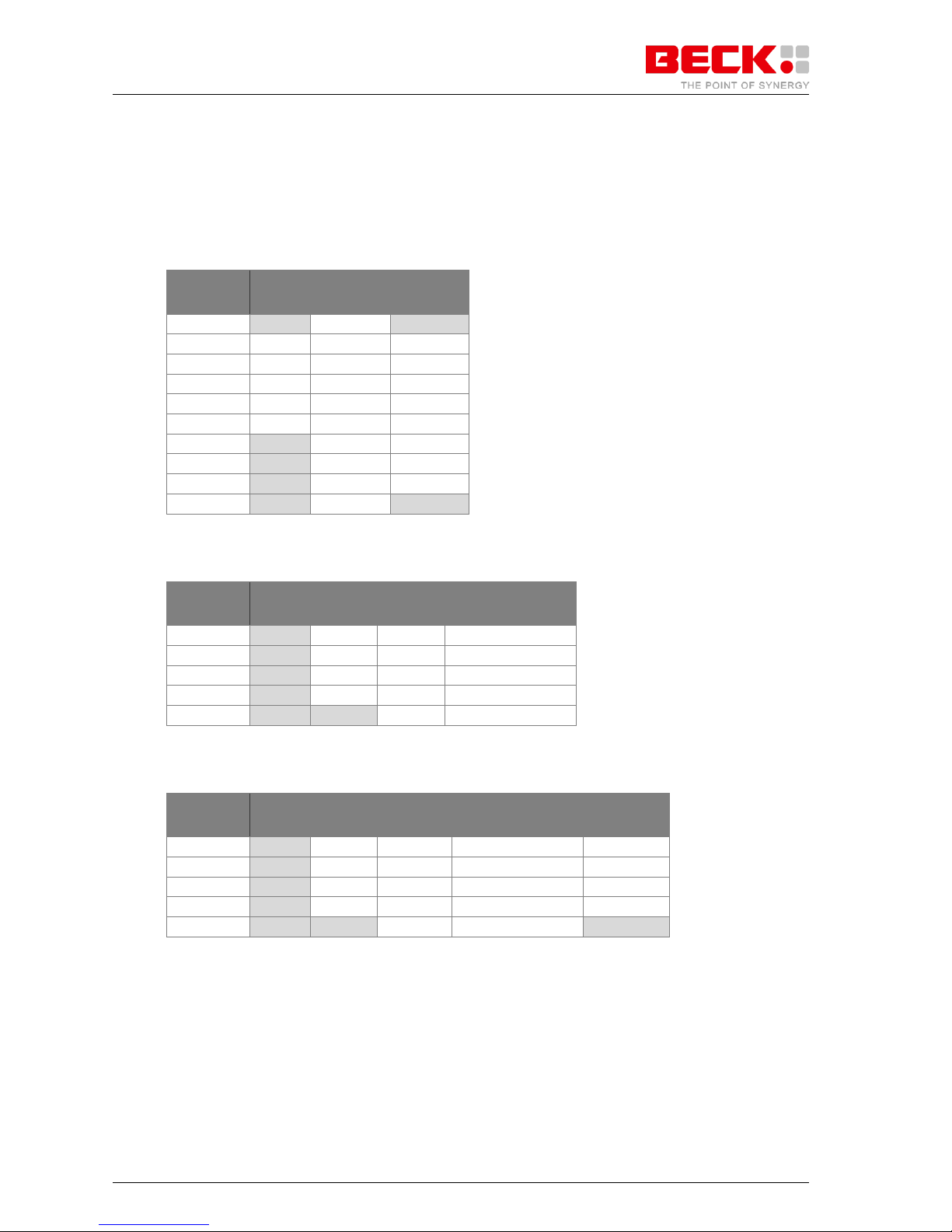
4.17 Programmable I/O Pins
The SC2x3 provides 40 programmable I/O pins. Each PIO can be programmed with the attributes function
(enabled/disabled) and direction (input/output). PIOs that programmed as output can drive 4mA (see chapter
8.2.4). During and after reset, all PIO pins are high impedance by default (except PIO0..PIO3, see chapter 6.2.2
Usage of PIO0..PIO3 in consideration of UART1 (Bootloader interface)).
The PIO pins cannot be enabled individually at all, e.g. if UART1 is used, PIO2 can’t be enabled as PIO
without disabling UART1. For more details see chapter 5 Mutal Exclusive Functions.
PIO Number
Shared Function Name
Group
Nr.
0
UART1_TXD
PSC1
0 1 UART1_RXD
PSC1
1 2 UART1_RTS
PSC1
2
3
UART1_CTS
PSC1
3
4
UART1_DCD
PSC1
4
5
UART2_TXD / CAN1TXD
PSC2
0 6 UART2_RXD / CAN1RXD
PSC2
1 7 UART2_RTS / CAN2TXD
PSC2
2 8 UART2_CTS / CAN2RXD
PSC2
3 9 UART2_DCD
PSC2 4 10
UART3_TXD / USB2_OE
PSC3 0 11
UART3_RXD / USB2_TXN
PSC3
1
12
UART3_RTS / USB2_TXP
PSC3 2 13
UART3_RXD / USB2_RXD
PSC3 3 14
UART3_DCD / USB2_RXP / LP_CS6#
PSC3 4 15
USB2_RXN / LP_CS7#
PSC3 5 16
MOSI / USB2_PRTPWR
PSC3 6 17
MISO / USB2_SPEED
PSC3 7 18
SS / USB2_SUSPEND
PSC3 8 19
SCK / USB2_OVRCNT
PSC3 9 20
UART6_RXD
PSC6 0 21
UART6_CTS
PSC6 1 22
UART6_TXD
PSC6
2
23
UART6_RTS
PSC6 3 24
USB1_OE
USB1 0 25
USB1_PRTPWR
USB1 6 26
USB1_SPEED
USB1 7 27
USB1_SUSPEND
USB1 8 28
USB1_OVRCNT
USB1 9 29
I2CCLK1
I2C
0
30
I2CDTA1
I2C
1
31
GPIO7 - -
32
TIMER0
TIMER 0 33
TIMER1
TIMER 1 34
TIMER2
TIMER 2 35
TIMER3
TIMER 3 36
TIMER4
TIMER 4 37
TIMER5
TIMER 5 38
TIMER6
TIMER 6 39
TIMER7
TIMER
7
Table 4-15: List of PIO sharing designations
Page 23
IPC@CHIP SC2x3
Hardware Manual V1.02 [01.03.09]
©2000-2009 BECK IPC GmbH Page 23
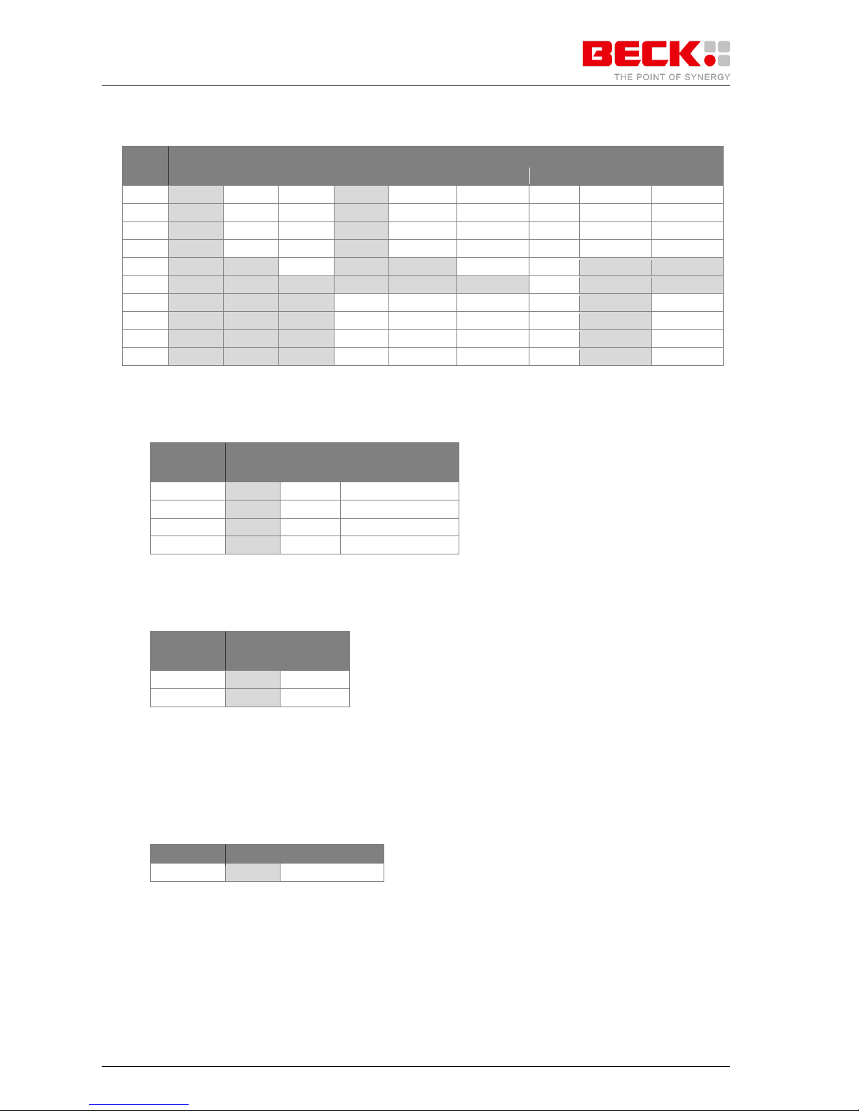
5 Mutal Exclusive Functions
The following tables are showing all valid combinations of pin functions. The pin functions can only configured
in columns and not separatly (except timers, see chapter 5.7 Mutal Exclusive Functions for TIMER).
5.1 Mutal Exclusive Functions for USB1
Function
USB1 Nr.
PIO
USB1
UART4/5
0
PIO24
OE
PIO24
1 - TXN
RTS 2 -
TXP
TXD
3 - RXD
RXD
4 - RXP
CTS 5 -
RXN
RXD
6
PIO25
PRTPWR
TXD
7
PIO26
SPEED
RTS
8
PIO27
SUSPEND
CTS
9
PIO28
OVERCNT
PIO28
Table 5-1: Mutal Exclusive Functions for USB1
5.2 Mutal Exclusive Functions for PSC1
Function
PSC 1 Nr.
PIO
UART1
UART1e
0
PIO0
TXD
TXD
CODEC1_TXD
1
PIO1
RXD
RXD
CODEC1_RXD
2
PIO2
RTS
RTS
PIO2
3
PIO3
CTS
CTS
CODEC1_CLK
4
PIO4
PIO4
DCD
CODEC1_FRAME
Table 5-2: Mutal Exclusive Functions for PSC1
5.3 Mutal Exclusive Functions for PSC2
Function
PSC 2 Nr.
PIO
UART2
UART2e
CODEC
CAN1/2
0
PIO5
TXD
TXD
CODEC2_TXD
CAN1TXD
1
PIO6
RXD
RXD
CODEC2_RXD
CAN1RXD
2
PIO7
RTS
RTS
PIO7
CAN2TXD
3
PIO8
CTS
CTS
CODEC2_CLK
CAN2RXD
4
PIO9
PIO9
DCD
CODEC2_FRAME
PIO9
Table 5-3: Mutal Exclusive Functions for PSC2
Page 24
IPC@CHIP SC2x3
Hardware Manual V1.02 [01.03.09]
©2000-2009 BECK IPC GmbH Page 24
5.4 Mutal Exclusive Functions for PSC3
PSC 3
Function
Nr.
PIO
UART3
UART3e
SPI
UART3/SPI
UART3e/SPI
USB2
CODEC
CODEC/SPI
0
PIO10
TXD
TXD
PIO10
TXD
TXD
OE
CODEC3_TXD
CODEC3_TXD
1
PIO11
RXD
RXD
PIO11
RXD
RXD
TXN
CODEC3_RXD
CODEC3_RXD
2
PIO12
RTS
RTS
PIO12
RTS
RTS
TXP
CODEC3_CLK
CODEC3_CLK
3
PIO13
CTS
CTS
PIO13
CTS
CTS
RXD
CODEC3_FRAME
CODEC3_FRAME
4
PIO14/CS6#
PIO14/CS6#
DCD
PIO14/CS6#
PIO14/CS6#
DCD
RXP
PIO14/CS6#
PIO14/CS6#
5
PIO15/CS7#
PIO15/CS7#
PIO15/CS7#
PIO15/CS7#
PIO15/CS7#
PIO15/CS7#
RXN
PIO15/CS7#
PIO15/CS7#
6
PIO16
PIO16
PIO16
MOSI
MOSI
MOSI
PRTPWR
PIO16
MOSI
7
PIO17
PIO17
PIO17
MISO
MISO
MISO
SPEED
PIO17
MISO
8
PIO18
PIO18
PIO18
SS
SS
SS
SUSPEND
PIO18
SS
9
PIO19
PIO19
PIO19
CLK
CLK
CLK
OVRCNT
PIO19
CLK
Table 5-4: Mutal Exclusive Functions for PSC3
5.5 Mutal Exclusive Functions for PSC6
Function
PSC 6 Nr.
PIO
UART6
0
PIO20
RXD
CODEC6_RXD
1
PIO21
CTS
CODEC6_FRAME
2
PIO22
TXD
CODEC6_TXD
3
PIO23
RTS
CODEC6_CLK
Table 5-5: Mutal Exclusive Functions for PSC1
5.6 Mutal Exclusive Functions for I2C
Function
I2C Nr.
PIO
I2C
0
PIO29
I2CCLK1
1
PIO30
I2CDTA1
Table 5-6: Mutal Exclusive Functions for I2C
5.7 Mutal Exclusive Functions for TIMER
Each timer (TIMER1-7) can be configured separately as timer or as PIO, inpependent from each other.
5.8 Mutal Exclusive Functions for Local Plus Bus
Function
PIO31
GPIO7/TSIZ[1]*
Table 5-7: Mutal Exclusive Functions for I2C
*GPIO7/TSIZ[1] is used to indicate the Transfer Size 1, see chapter4.2 Address-/Data Bus
Page 25

IPC@CHIP SC2x3
Hardware Manual V1.02 [01.03.09]
©2000-2009 BECK IPC GmbH Page 25
6 Functional Description
6.1 Local Plus Bus
6.1.1 Features
The LocalPlus has the following features:
Interface to chip selected devices
Two main modes of operation:
- non-MUXed Modes
Legacy Modes (Address 8, 16, or 24 bits, Data 8 or 16 bits)
Most Graphics Mode (Address 24 bits, Data 32 bits)
Large Flash Mode (Address 26 bits, Data 8 or 16 bits)
- MUXed Modes
(Address 8, 16, 24 or 25 bits, Data 8,16 or 32 bits, 2 Bank Selects)
2 Chip Select (CS) signals
- Programmable Wait States per CS
- Programmable Deadcycles per CS
- Programmable Byte Swapping per CS
Dynamic bus sizing on some interfaces
Support of BURST MODE FLASH devices
DMA (BestComm) support allows data movement independently from the CPU
NO support of misaligned accesses
6.1.2 Interface
The LocalPlus interface consists of:
Address bus
Data bus
Chip select signals CS1, 3, 4, 5, 6 and 7
Control signals:
- R/W (Read/Write)
- ALE (Address Latch Enable)
- ACK (Acknowledge)
- TS (Transfer Start)
- OE (Output Enable)
- TSIZ bits (Transfer Size)
- Bank Select bits
Reference clock PCI_CLOCK
The reference clock PCI_CLOCK is always running, even if the PCI Controller is disabled.
Page 26

IPC@CHIP SC2x3
Hardware Manual V1.02 [01.03.09]
©2000-2009 BECK IPC GmbH Page 26
6.1.3 External Local Plus Bus Signals
Signal
I/O
Definition
LP_CS1#,
LP_CS3#.. LP_CS7#
O
Chip Selects (active low), CS[4] and CS[5] shared with ATA, CS[6] and
CS[7] shared with PSC3.
LP_RW
O
Read/Write. 1 = Read, 0 = Write
EXT_AD[31:0]
I/O
AD Address / Data bus (bi-directional when used as data; bit 31=msb)
LP_ACK#
I/O
External Acknowledge input (non-burst transactions),
BURST indication for Most Graphics or Large Flash Modes (Open Drain)
LP_TS#
O
Transfer Start
LP_OE#
O
Output Enable
TSIZ[1:2]
O
Transfer Size
TSIZ bits are available in non-muxed modes on GPIO7 and TEST_SEL_1
pins.
The MUXed Mode provides 3 bits TSIZ[0:2], which are available on
EX_AD[30:28].
LP_ALE#
O
Address Latch Enable
Table 6-1: External Local Plus Bus Signals
Page 27

IPC@CHIP SC2x3
Hardware Manual V1.02 [01.03.09]
©2000-2009 BECK IPC GmbH Page 27
6.1.4 Local Plus Bus Address / Data Pin Assignments
Non-Muxed Mode Muxed Mode
16 Bit Adr,
16 Bit Data
24 Bit Adr,
8 Bit Data
Address
tenures
8 Bit Data
tenure
16 Bit Data
tenure
32 Bit Data
tenure
EXT_AD[31]
D15
D7 0
D7
D15
D31
EXT_AD[30]
D14
D6
TSIZ[2]
D6
D14
D30
EXT_AD[29]
D13
D5
TSIZ[1]
D5
D13
D29
EXT_AD[28]
D12
D4
TSIZ[0]
D4
D12
D28
EXT_AD[27]
D11
D3 0
D3
D11
D27
EXT_AD[26]
D10
D2
BS1
D2
D10
D26
EXT_AD[25]
D9
D1
BS0
D1
D9
D25
EXT_AD[24]
D8
D0 A24
D0
D8
D24
EXT_AD[23]
D7
A23
A23 0 D7
D23
EXT_AD[22]
D6
A22
A22 0 D6
D22
EXT_AD[21]
D5
A21
A21 0 D5
D21
EXT_AD[20]
D4
A20
A20 0 D4
D20
EXT_AD[19]
D3
A19
A19 0 D3
D19
EXT_AD[18]
D2
A18
A18 0 D2
D18
EXT_AD[17]
D1
A17
A17 0 D1
D17
EXT_AD[16]
D0
A16
A16 0 D0
D16
EXT_AD[15]
A15
A15
A15 0
D15
EXT_AD[14]
A14
A14
A14
0
D14
EXT_AD[13]
A13
A13
A13 0
D13
EXT_AD[12]
A12
A12
A12
0
D12
EXT_AD[11]
A11
A11
A11 0
D11
EXT_AD[10]
A10
A10
A10
0
D10
EXT_AD[9]
A9
A9 A9 0
D9
EXT_AD[8]
A8
A8 A8 0
D8
EXT_AD[7]
A7
A7 A7
D7
EXT_AD[6]
A6
A6 A6
D6
EXT_AD[5]
A5
A5 A5
D5
EXT_AD[4]
A4
A4 A4
D4
EXT_AD[3]
A3
A3 A3
D3
EXT_AD[2]
A2
A2 A2
D2
EXT_AD[1]
A1
A1 A1
D1
EXT_AD[0]
A0
A0 A0
D0
Table 6-2: Local Plus Bus Address / Data Pin Assignments
Page 28

IPC@CHIP SC2x3
Hardware Manual V1.02 [01.03.09]
©2000-2009 BECK IPC GmbH Page 28
6.2 Programmable Serial Controllers
The SC2x3 supports six PSCs (Programmable Serial Controllers). Each can be configured to operate in
different modes. PSCs support both synchronous and asynchronous protocols. They are used to interface,
modems, SPI or CAN.
6.2.1 UARTs
The SC2x3 provides six asynchronous serial ports through the PSCs. These ports provide full-duplex,
bidirectional data transfer using several industry-standard communications protocols.
The asynchronous serial ports support the following features:
Full-duplex operation
512 byte FIFO
7-bit or 8-bit data transfers
Odd, even, mark, space, no parity or multidrop mode
One or two stop bits
Long or short break character recognition
Error detection
- Parity errors
- Framing errors
- Overrun errors
- Break character recognition
Hardware handshaking with the following selectable control signals:
- Clear-to-send (CTS)
- Ready-to-send (RTS)
- Data Carrier Detect (DCD)
Separate maskable interrupts for each port
Independent baud rate generators
Maximum baud rate of 4.125 MBits/s
Double-buffered transmit and receive
Page 29
IPC@CHIP SC2x3
Hardware Manual V1.02 [01.03.09]
©2000-2009 BECK IPC GmbH Page 29
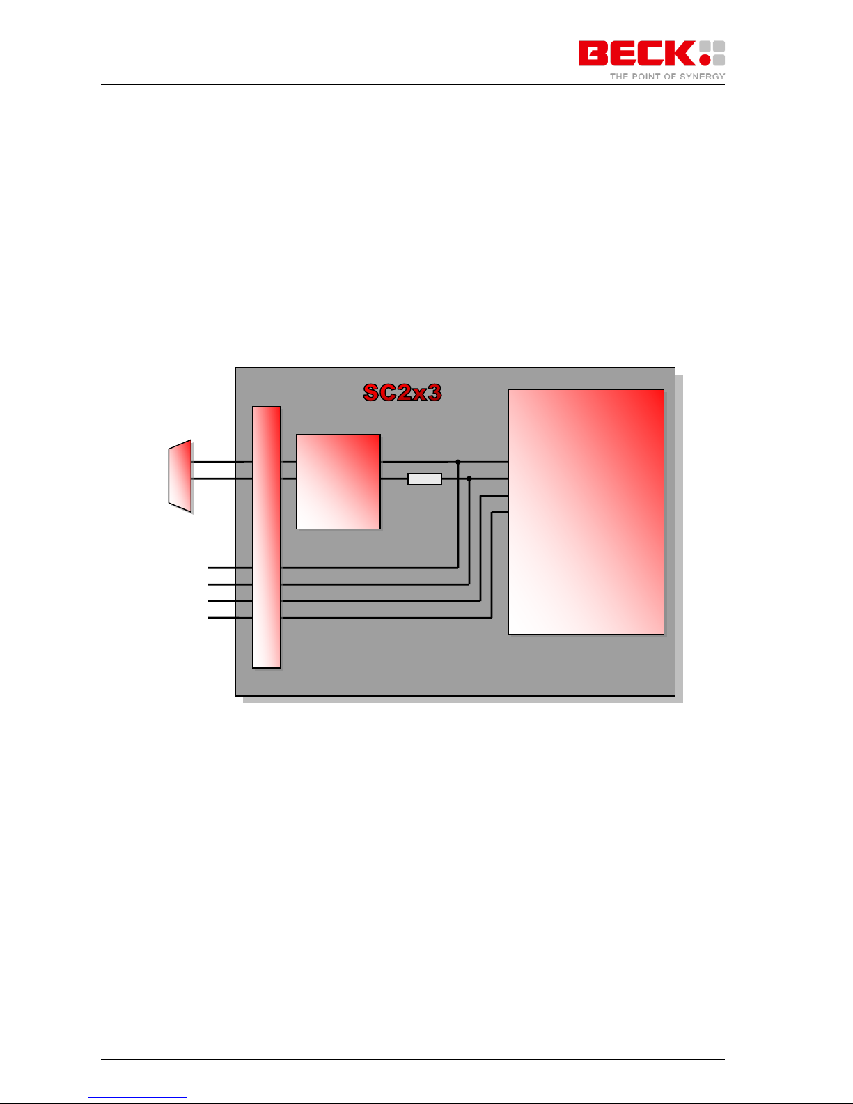
6.2.2 Usage of PIO0..PIO3 in consideration of UART1 (Bootloader interface)
The RTOS version can be updated via UART1 and the Ethernet interface.
In some rare cases a system crash can corrupt the RTOS image on the flash disk. If the RTOS is damaged
and doesn’t boot anymore, a update through Ethernet will not work. Without a working RTOS it can only be
repaired by programming it through the serial bootloader interface on UART1.
For this reason the pre-installed bootloader observes UART1_TXD and UART1_RXD to recognize a RTOS
update via the program Chiptool. To do this, the bootloader initializes UART1 and the corresponding pins will
be active while booting and not high impedance!
This has to be considered, if PIO0..PIO3 is used. The following figure shows a block diagram of the internal
schematic of the SC2x3.
Figure 6-1: Internal block diagram of PIO0..PIO3 and UART1
CPU
Transceiver
TXD/PIO0
RXD/PIO1
5K6
RTS/PIO2
CTS/PIO3
X1
PIO0
PIO1
PIO2
PIO3
UART1
TXD
RXD
Page 30

IPC@CHIP SC2x3
Hardware Manual V1.02 [01.03.09]
©2000-2009 BECK IPC GmbH Page 30
6.2.3 I²C
The I²C bus is a popular serial, two-wire interface used in many systems because of its low overhead. Capable
of 100 kHz operation, each device connected to the bus is software addressable by a unique address, with a
simple master/slave protocol.
The I²C bus consists of two wires, serial data (SDA), and a serial clock (SCL), which carry information between
the devices connected to the bus. This two-wire interface minimizes interconnections, so integrated circuits
have fewer pins, and the number of traces required on printed circuit boards is reduced.
The number of devices connected to the same bus is limited only by a maximum bus capacitance of 400 pF.
Both the SDA and SCL lines are bidirectional, connected to a positive supply voltage via a 2.2k pull-up
resistor. When the bus is free, both lines are HIGH. The output stages of devices connected to the bus must
have an open-drain or open-collector to perform the wired-AND function.
Each device on the bus has a unique address and can operate as either a transmitter or receiver. In addition,
devices can also be configured as masters or slaves.
A master is the device that initiates a data transfer on the bus and generates the clock signals to permit
that transfer.
Any other device that is being addressed is considered a slave.
The I²C protocol defines an arbitration procedure to ensure that if more than one master simultaneously tries to
control the bus, only one is allowed to do so and the message is not corrupted.
The SC2x3 supports two I²C channels. Both master and slave interfaces can be controlled directly by the
processor. The arbitration and clock synchronization procedures defined in the I²C specification are supported
by the SC2x3 I²C controller. The following features are provided:
Master or slave operation
Multimaster operation
Software selectable acknowledge bit
Arbitration-lost interrupt with automatic mode switching from master to slave
Calling address identification interrupt with automatic mode switching from master to slave
START and STOP signal generation/detection
Repeated START signal generation
Acknowledge bit generation/detection
Bus busy detection
more than 100 kHz operation
Programmable Glitch Filter
Note: On the I2C2 bus interface there are some internal devices present. So the following addresses can not be
used externally: 0xA0, 0x90.
Page 31

IPC@CHIP SC2x3
Hardware Manual V1.02 [01.03.09]
©2000-2009 BECK IPC GmbH Page 31
6.2.4 USB
The SC2x3 supports two USB channels. The USB Controller implements the USB Host Controller/Root Hub in
compliance with the USB1.1 specification. The user may choose to have either one or two USB ports on the
root hub, each of which can interface to an off-chip USB transceiver. The Host Controller supports the Open
Host Controller Interface (OHCI) standard.
The interface has an integrated DMA controller that transfers packet data to and from memory. The DMA
controller facilitates USB endpoint data transfer efficiently, while limiting microprocessor involvement.
6.2.5 SPI
SPI is a high-speed synchronous serial input/output (I/O) port that allows a serial bit stream of programmed
length (one to eight bits) to be shifted into and out of the device at a programmable bit-transfer rate.
SPI is an industry-standard communications interface that does not have specifications or a standards
organizing group. As a result, there are no licensing requirements. Because of its simplicity, SPI is commonly
used in embedded systems. Many semiconductor manufacturers sell a variety of sensor, conversion, and
control devices that use SPI.
The SPI module allows full-duplex, synchronous, serial communication between the SC2x3 and peripheral
devices. The clock polarity, clock phase, SS (Slave Select) polarity, clock frequency in master mode, and the
number of bits to be transferred are software programmable up to 66MHz. SPI supports multiple slaves on a
single 3-wire bus by using separate Slave Select signals to enable the desired slave.
Page 32

IPC@CHIP SC2x3
Hardware Manual V1.02 [01.03.09]
©2000-2009 BECK IPC GmbH Page 32
6.2.6 CAN
The SC2x3 contains two complete CAN 2.0B controllers, CAN1 and CAN2. Each controller supplies two signal
pins, CAN Receive (CANRXD) and CAN Transmit (CANTXD). These signals can be connected to a CAN
transceiver.
The CAN controllers can be accessed through the RTOS API functions. In addition to the Run mode, the
controllers can be used in Loop Back mode or Passive mode. In Loop Back mode both CAN channels are
internally connected with themselves. This can be useful for software testing. In Passive mode the controllers
are only listening. The output is held recessively. The Run mode is the normal operating mode.
Various baud rates are provided. The following table shows the most common possible baud rates. For more
information to provided baud rates see RTOS API documentation.
50 KBit/s
125 KBit/s
250 KBit/s
500 KBit/s
1 MBit/s
Table 6-3: Provided CAN baud rates
The basic features of the CAN controllers are as follows:
Implementation of the CAN protocol - Version 2.0A/B
- Standard and extended data frames
- 0 - 8 bytes data length
- Programmable bit rate up to 1 Mbps
- Support for remote frames
- 4 receive buffers with FIFO storage scheme
3 transmit buffers with internal prioritization using a ―local priority‖ concept
Flexible maskable identifier filter supports two full size extended identifier filters (two 32-bit) or four 16-bit
filters or eight 8-bit filters
Programmable loop back mode supports self-test operation
Programmable listen-only mode for monitoring of CAN bus
Separate signalling and interrupt capabilities for all CAN receiver and transmitter error states (Warning,
Error Passive, Bus-Off)
Page 33

IPC@CHIP SC2x3
Hardware Manual V1.02 [01.03.09]
©2000-2009 BECK IPC GmbH Page 33
6.3 Timers
Seven General-Purpose Timer (GPT) pins are configurable for:
Input Capture
Output Compare
Pulse Width Modulation (PWM) Output
Simple GPIO
Internal CPU timer
The timer modules run off the internal IP bus clock. Each Timer is associated to a single I/O pin. Each Timer
has a 16-bit prescaler and 16-bit counter, thus achieving a 32-bit range (but only 16-bit resolution).
6.4 MII Interface
The SC2x3 provides an Fast Ethernet controller. The main function of the MII interface is to provide a
communication path between the internal MAC and an external PHY.
The Ethernet Controller supports a 100 Mbps IEEE 802.3 MII MAC-PHY interface. It is full duplex and provides
a programmable maximum frame length and retransmission from the Tx FIFO following a collision.
6.5 Reset
The Reset-Logic of the module has the following functions:
Monitoring the voltage used on the module (3.3V, 1.8V, 1.5V)
External Reset-Input
Battery back up function for SRAM (Battery supply not on the module)
Chip-Select-Gating for battary powered SRAM
Reset-Status-Display through a red LED
The SC2x3 has these four reset pins:
RESIN# - Master Reset Input
The Master Reset Input performs the power-on reset. This
resets the whole module.
PORRESET# - Power-on Reset
The power-on reset is an output, wich indicates the
master/power-on reset. It forces HRESET# and SRESET#
active.
HRESET# - Hard Reset
The hard reset is a bidrectional signal with a Schmitt-Trigger
input and open drain pullup including an internal resistor. It can
be asserted by an external source or it can be asserted by the
internal reset logic of the SC2x3.
HRESET# forces SRESET active.
SRESET# - Software Reset
The soft reset is a bidrectional signal with a Schmitt-Trigger
input and open drain pullup including an internal resistor. It can
be asserted by an external source or it can be asserted by the
internal reset logic of the SC2x3.
Page 34

IPC@CHIP SC2x3
Hardware Manual V1.02 [01.03.09]
©2000-2009 BECK IPC GmbH Page 34
7 System interrupts
Source
Sensitivity
0
IRQ0
level high/level low/rising edge/falling edge
1
IRQ1
level high/level low/rising edge/falling edge
2
IRQ2
level high/level low/rising edge/falling edge
3
IRQ3
level high/level low/rising edge/falling edge
4-5
reserved
-
6
SliceTimer0
-
7-10
reserved
-
11
Timer1
-
12
Timer2
-
13
Timer3
-
14
Timer4
-
15
Timer5
-
16
Timer6
-
17
Timer7
-
18-19
reserved
-
20
PSC1_4/PIO4
any transition/pulse/rising edge/falling edge
21
PSC2_4/PIO9
any transition/pulse/rising edge/falling edge
22
PSC3_4/PIO14
any transition/pulse/rising edge/falling edge
23
PSC3_5/PIO15
any transition/pulse/rising edge/falling edge
24
PSC3_8/PIO18
any transition/pulse/rising edge/falling edge
25
PSC3_9/PIO19
any transition/pulse/rising edge/falling edge
26
PSC6_0/PIO20
any transition/pulse/rising edge/falling edge
27
PSC6_1/PIO21
any transition/pulse/rising edge/falling edge
28
USB1_9/PIO28
any transition/pulse/rising edge/falling edge
29
GPIO_7/PIO31
any transition/pulse/rising edge/falling edge
30-31
reserved
-
32
SPI controller (slave mode)
-
33
I2C1 controller (slave mode)
-
34
I2C2 controller (slave mode)
-
7.1 Watchdog
The SC2x3 provides a true watchdog timer function. The watchdog can be used to regain control of the system
when software fails to respond as expected. The watchdog is active after reset. The watchdog timeout period is
about 800 ms. The mode can be set to trigger the watchdog by the user program or by the CHIP-RTOS
(default). In CHIP-RTOS mode, the CHIP-RTOS performs the watchdog strobing provided that the system's
timer interrupt is allowed to execute. Beware that excessive interrupt masking periods can lead to system
resets.
Page 35
IPC@CHIP SC2x3
Hardware Manual V1.02 [01.03.09]
©2000-2009 BECK IPC GmbH Page 35
8 Characteristics
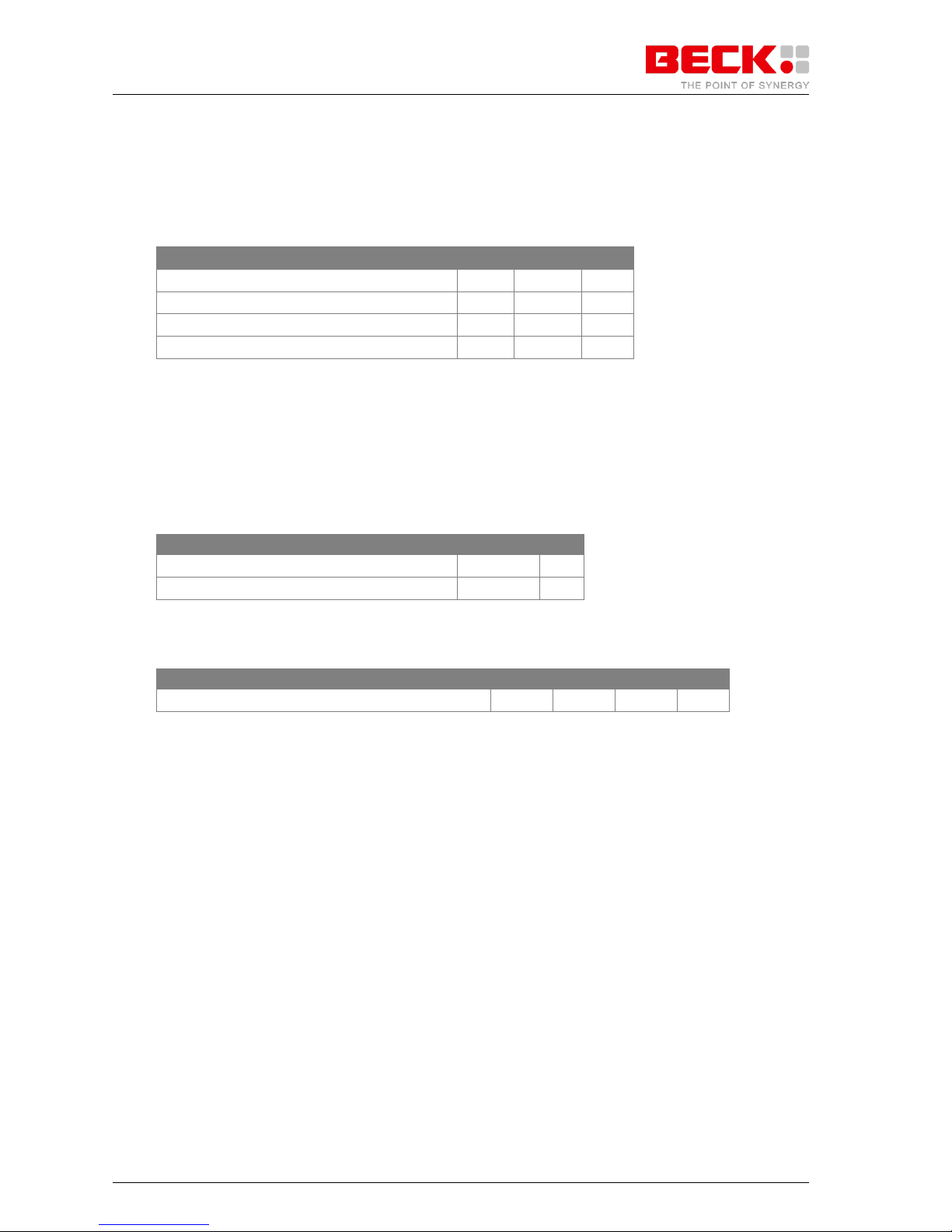
8.1 Absolute Maximum Ratings
Parameter
Min
Max
Unit
Supply Voltage (VCC)
3.06
3,6
V
Storage Temperature
-55°C
+100°C
°C
Supply current (VCC = 3.6V)
1,6
A
Voltage on any pin with respect to ground
-0.3
VCC+0.3
V
Table 8-1: Absolute Maximum Ratings
8.2 Recommended Operating Ranges
8.2.1 Voltage and Temperature
(Under operating ranges unless otherwise noted)
Note: Exposure to conditions beyond those listed here may adversely affect the lifetime and reliability of the
device.
Parameter
Unit
Supply Voltage (VCC)
3.3 ±5%
V
Operating Temperature
-40..+85°C
°C
Table 8-2: Recommended Operating Ranges
8.2.2 Supply Current
Parameter
Min
Typ
Max
Unit
Current into VCC @3,3V
0,6 A
Table 8-3: Supply Current
Page 36
IPC@CHIP SC2x3
Hardware Manual V1.02 [01.03.09]
©2000-2009 BECK IPC GmbH Page 36
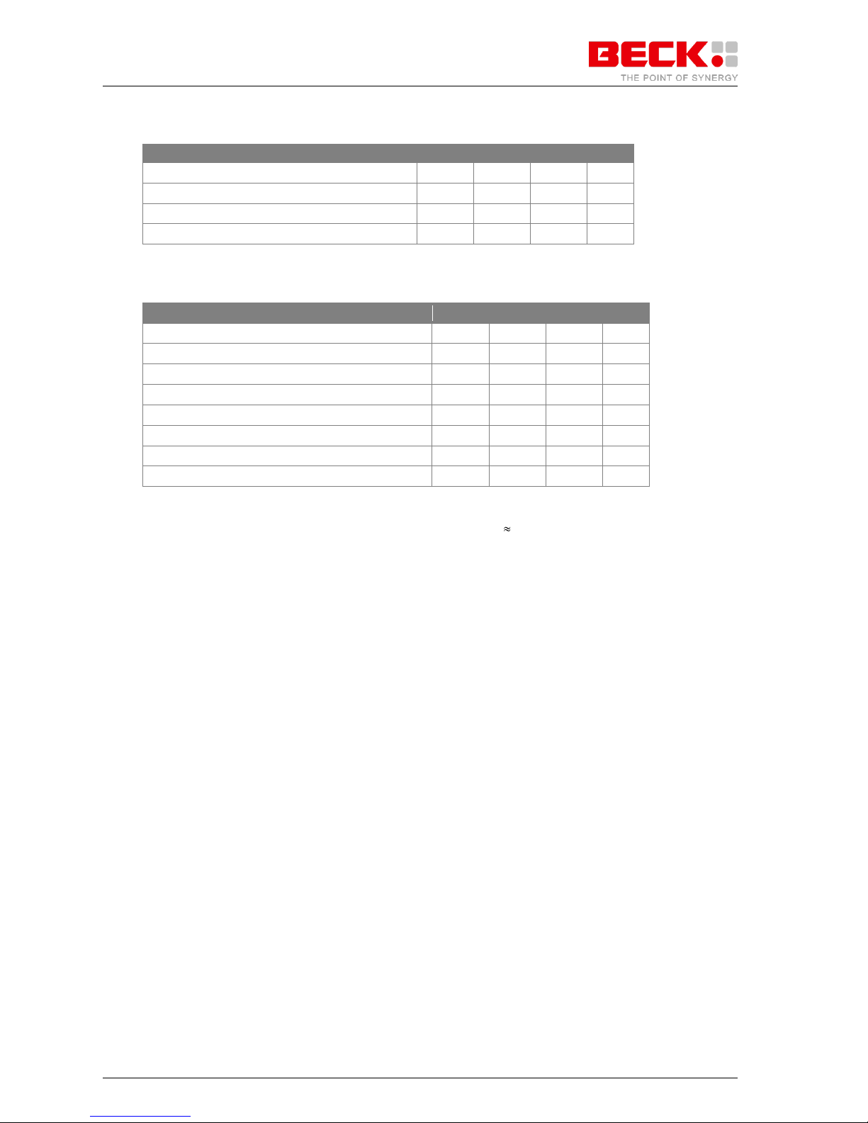
8.2.3 Inputs
Parameter
Min
Typ
Max
Unit
VIL Input Low Voltage
0.8
V
VIH Input High Voltage
2.0 V IINPU Input current, pullup resistor
40 109
µA
IINPD Input current, pulldown resistor
36 106
µA
Table 8-4: Inputs
8.2.4 Outputs
Parameter
Min
Typ
Max
Unit
VOL Output Voltage Low @IOL max
0.4
V
VOH Output Voltage High @IOH max
2.4 V Low level output current @VOL 0.4V [4mA]
4
mA
Low level output current @VOL 0.4V [8mA]
8
mA
Low level output current @VOL 0.4V [16mA]
16 mA
High level output current @VOH 2.4V [4mA]
4
mA
High level output current @VOH 2.4V [8mA]
8
mA
High level output current @VOH 2.4V [16mA]
16 mA
Table 8-5: Outputs
Note: [..mA] describes the driver category. E. g. [4mA] can source 4mA.
Page 37
IPC@CHIP SC2x3
Hardware Manual V1.02 [01.03.09]
©2000-2009 BECK IPC GmbH Page 37
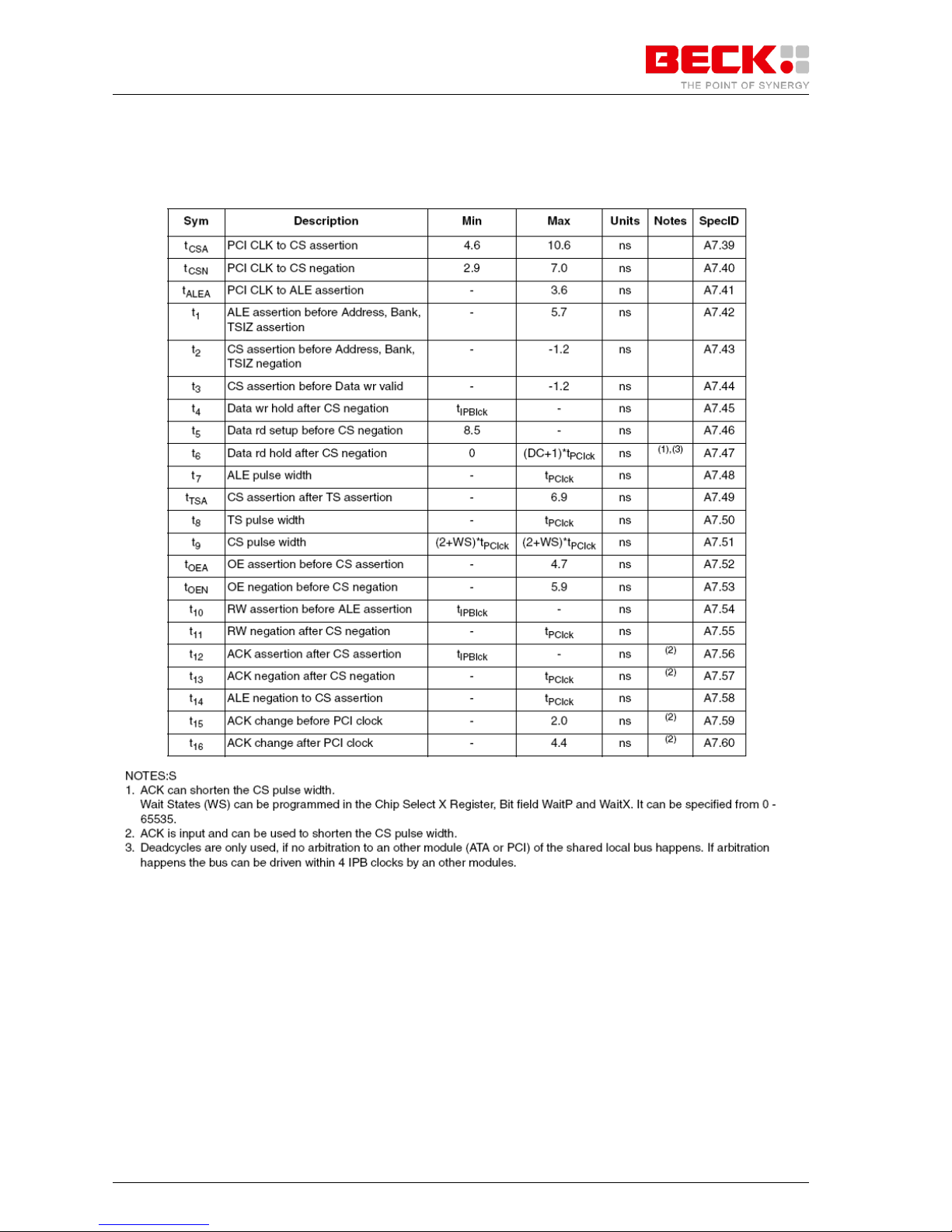
8.3 AC Characteristics
8.3.1 Muxed Mode
Figure 8-1: Timing Diagram – MUXed Mode
Rastereinstellungen:
Abstand horizontal: 0,15
Abstand vertikal: 0,3
1 Kästchen=0,5ns ?
Page 38
IPC@CHIP SC2x3
Hardware Manual V1.02 [01.03.09]
©2000-2009 BECK IPC GmbH Page 38
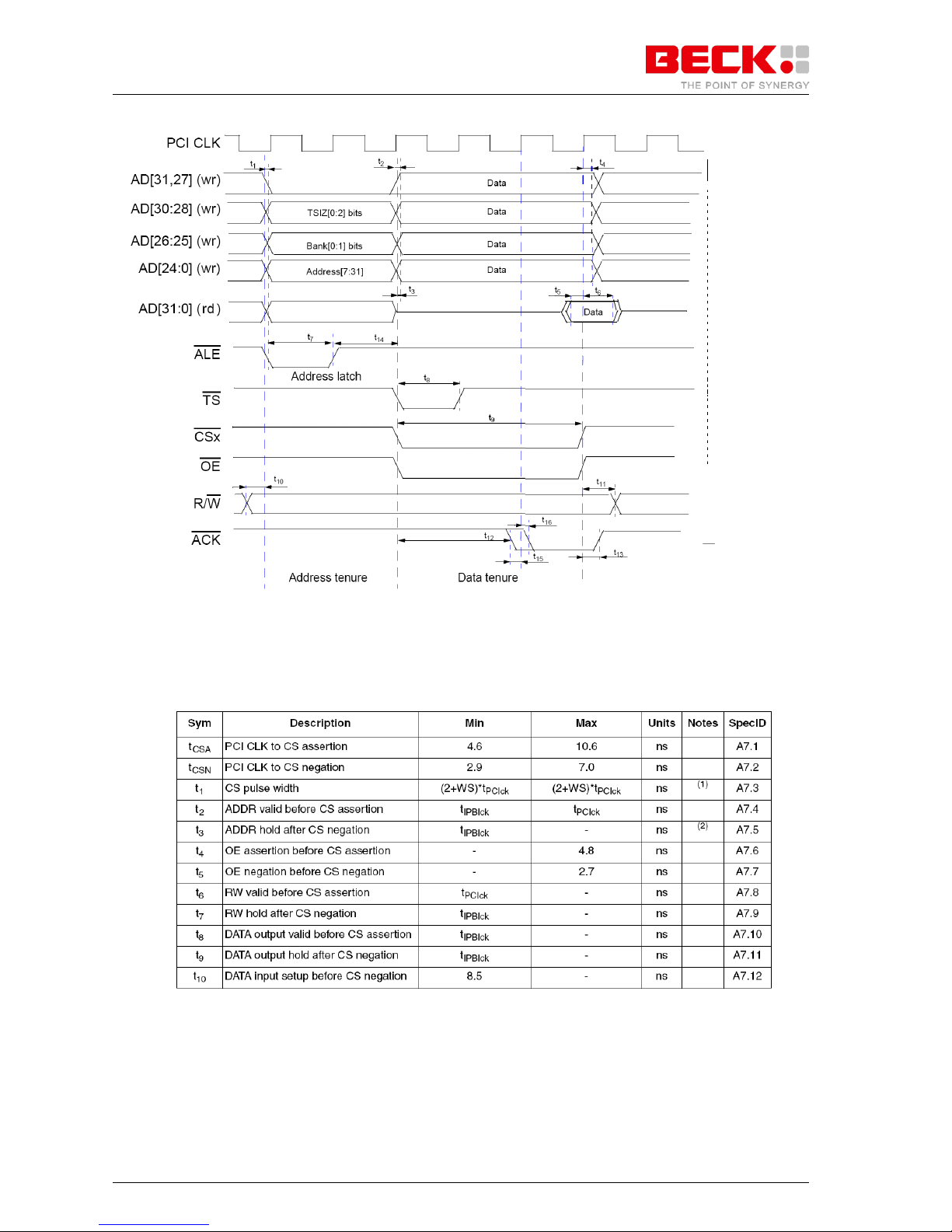
Figure 8-2: Timing Diagram–MUXed Mode
8.3.2 Non-Muxed Mode
Page 39
IPC@CHIP SC2x3
Hardware Manual V1.02 [01.03.09]
©2000-2009 BECK IPC GmbH Page 39
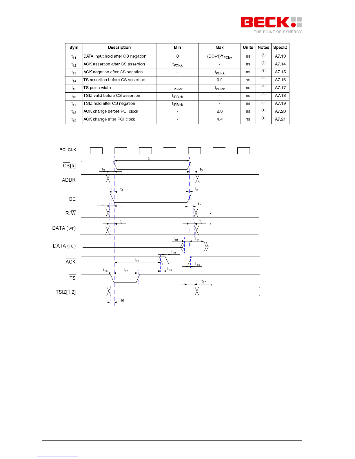
Figure 8-3: Timing Diagram–Non-MUXed Mode
Page 40
IPC@CHIP SC2x3
Hardware Manual V1.02 [01.03.09]
©2000-2009 BECK IPC GmbH Page 40
9 Package Information
9.1 Dimensions
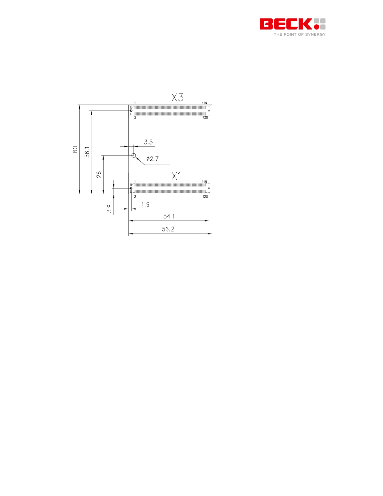
Figure 9-1: Package Dimensions. Top view through the conductor board.
9.2 SC2x3 Connector
Board-to-Board-connection via a 120-pole connector with 0.8-mm spacing.
Manufacturer: AMP
Component: 5179031-5
Base board connectors are available in different heights.
Page 41

IPC@CHIP SC2x3
Hardware Manual V1.02 [01.03.09]
©2000-2009 BECK IPC GmbH Page 41
10 Custom series programming of SC2x3
The program chiptool.exe can be used to program images to the SC2x3. Chiptool can be started and
configured through command line parameters. This can be used to remote chiptool from other applications to
program SC2x3 in series with high quantities.
Chiptool also can program up to eight IPC@CHIPs parallel by using a PC with eight serial RS232 ports.
See chiptool help file for more information.
Page 42
IPC@CHIP SC2x3
Hardware Manual V1.02 [01.03.09]
©2000-2009 BECK IPC GmbH Page 42
11 History
Revision
Date
Author
Comments
V0.90
12.03.09
M.Nesseldreher
Initial version
V0.91
03.04.09
Chapter 5.4 Mutal Exclusive Functions for PSC3, added
PIOs
27.05.09
Chapter 3 Added components to block diagram
27.10.09
Added chapter 6.1.4
27.10.09
Added Codec Modi for PSC1,2 and 6
1.00
25.11.09
Chapter 4.11 MII Interface, wrong RXER pin number
1.01
15.12.09
Chapter ―Interrupts‖ added.
Pullup/down values added.
11.03.10
changed hole size in figure 4-1
© 2000-2009 BECK IPC GmbH All rights reserved. No part
of this document may be copied or reproduced in any form or by
any means without the prior written consent of BECK IPC
GmbH. The information in this document is subject to change
without notice. Devices sold by BECK IPC GmbH. Are covered
by warranty and patent indemnification provisions appearing in
BECK IPC GmbH. Terms and Conditions of Sale only. BECK
IPC GmbH MAKES NO WARRANTY, EXPRESS,
STATUTORY, IMPLIED OR BY DESCRIPTION, REGARDING
THE INFORMATION SET FORTH HEREIN OR REGARDING
THE FREEDOM OF THE DESCRIBED DEVICES FROM
INTELLECTUAL PROPERTY INFRINGEMENT. BECK IPC
GmbH MAKES NO WARRANTY OF MERCHANTABILITY OR
FITNESS FOR ANY PURPOSE.
BECK IPC GmbH Shall not is responsible for any errors that
may appear in this document. BECK IPC GmbH makes no
commitment to update or keep current the information
contained in this document.
Life critical applications — These products are not designed for
use in life support appliances, aeronautical applications or
devices or systems where malfunction of these products can
reasonably be expected to result in personal injury.
Right to make changes — BECK IPC GmbH reserves the right
to make changes, without notice, in the products, including
software, described or contained herein in order to improve
design and/or performance. Beck IPC GmbH assumes no
responsibility or liability for the use of any of these products.
 Loading...