

Page 1
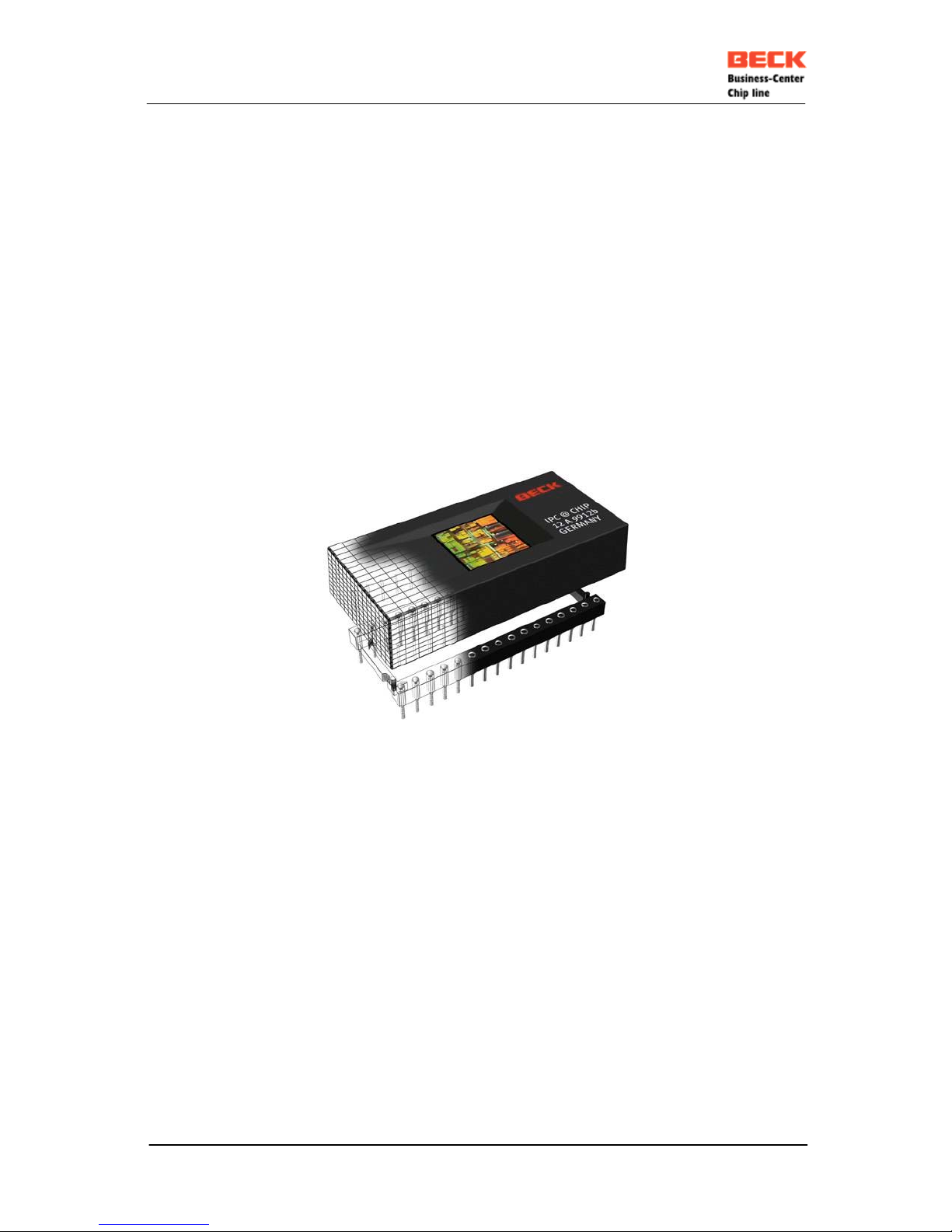
IPC@CHIP - SC12
Hardware Manual v1.1 [05.11.2002]
©BECK IPC GmbH page 1 of 28
Preliminary
Hardware Manual
High Performance, 80186- and 80188-Compatible,
16-Bit Embedded Microcontroller
Single Chip PC with Ethernet 10Base-T, Flash, RAM, Watchdog
Page 2

IPC@CHIP - SC12
Hardware Manual v1.1 [05.11.2002]
©BECK IPC GmbH page 2 of 28
Table of Contents
Page
1. BASIC SPECIFICATIONS ........................................................................................................3
2. PHYSICAL DIMENSIONS.........................................................................................................5
3. PIN CONFIGURATION .............................................................................................................6
4. PIN FUNCTIONS ......................................................................................................................7
4.1 Address / Data bus.......................................................................................................7
4.2 Programmable I/O Pins................................................................................................8
4.3 Programmable Chip Selects ........................................................................................9
4.4 Interrupts ......................................................................................................................9
4.5 Timer ..........................................................................................................................10
4.6 10Base-T Interface.....................................................................................................10
4.7 Asynchronous Serial Ports.........................................................................................10
4.8 DMA............................................................................................................................11
4.9 I2C-Bus .......................................................................................................................12
4.10 Reset, Power Fail Generator......................................................................................12
5. MUTUAL EXCLUSIVE FUNCTIONS ......................................................................................15
6. ETHERNET 10BASE-T...........................................................................................................17
6.1 10Base-T Media Filter Placement and Termination...................................................17
6.2 Magnetics approved for use for 10Base-T application...............................................17
7. SYSTEM OVERVIEW .............................................................................................................18
7.1 Memory map ..............................................................................................................18
7.2 System interrupts .......................................................................................................19
7.3 Watchdog ...................................................................................................................19
8. CHARACTERISTICS ..............................................................................................................20
8.1 ABSOLUTE MAXIMUM RATINGS.............................................................................20
8.2 OPERATING RANGES..............................................................................................20
8.3 DC-CHARACTERISTICS...........................................................................................20
8.4 AC-CHARACTERISTICS ...........................................................................................21
8.4.1 Read Cycle.................................................................................................................21
8.4.2 Write Cycle .................................................................................................................22
8.4.3 Interrupt Acknowledge Cycle .....................................................................................22
9. ENVIRONMENTAL TEST.......................................................................................................23
10. APPLICATION EXAMPLES....................................................................................................24
10.1 NMI / Reset-in / Link-LED ..........................................................................................24
10.2 Link-LED / Reset ........................................................................................................25
10.3 256x 8bit I/O-Extension using 74HCT573/245...........................................................25
10.4 Connect 10Base-T Ethernet to the SC12...................................................................26
11. ERRATA LIST .........................................................................................................................27
Page24, Chapter 10.1 NMI / Reset-In / Link-LED..................................................................27
Page 19, Chapter 7.3 Watchdog.............................................................................................27
Page25, Chapter 10.2 Link-LED / Reset.................................................................................27
Page14, Chapter 4.10 Reset, Power Fail Generator ..............................................................27
12. CONTACT...............................................................................................................................28
Page 3

IPC@CHIP - SC12
Hardware Manual v1.1 [05.11.2002]
©BECK IPC GmbH page 3 of 28
1. BASIC SPECIFICATIONS
@CHIP CPU RAM FLASH Ethernet
SC12 80186 20MHz 512 Kbytes 512 Kbytes 10Base-T
IPC@CHIP® family 80186- and 80188-compatible microcontroller with up to 512KB-RAM, 512KB
Flash and Ethernet on Chip
- Lower system cost with higher performance
High performance
- 20-MHz operating frequency
- Zero-wait-state operation at 20 MHz (RAM)
- 1-Mbyte internal memory space
- 6 x 256-byte I/O space
- Low-power CMOS process with single 5V power supply
Enhanced integrated peripherals
- Up to 14 programmable I/O (PIO) pins
- Two full-featured asynchronous serial ports allow full-duplex, 7-bit, 8-bit, or 9-bit data transfers,
Serial port hardware handshaking with CTS and RTS selectable for each port
Independent serial port baud rate generators
DMA to and from the serial ports
- Ethernet controller for IEEE 802.3, 10Base-T,
Integrated 10Base-T transceiver (SC12 only)
Auto-Polarity detection and correction
Loopback capability for diagnostics
Receiver and collision squelch circuit to reduce noise
Built-in pre-distortion resistors for 10Base-T application
- Watchdog timer
- Pulse-width demodulation option
Familiar 80C186 peripherals
- Two independent DMA channels
- Programmable interrupt controller with up to six external interrupts
- Three programmable 16-bit timers, the 2 input timers are interrupt capable
- Programmable memory and peripheral chip-select logic
Software-compatible with the 80C186 and 80C188 microcontrollers with widely available native
development tools, applications, and system software
Available in the following packages:
- 32-pin, plastic pack (DIL32)
The @CHIP SC12 microcontrollers are part of the Beck IPC@CHIP® family of System on Chip
microcontrollers and microprocessors based on the x86 architecture. The IPC@CHIP family
microcontroller is the ideal solution for new designs requiring Ethernet TCP/IP communication over
twisted pair and/or through the serial port. The compatibility with the 80C186/188 family makes it also
an ideal upgrade for systems based upon this processor range but requiring increased performance,
serial communications, Ethernet communications, a direct bus inter-face, or more than 64K of
memory.
The IPC@CHIP family microcontrollers integrates up to 512Kbyte DRAM with increased
performance and up to 512Kbyte FLASH reducing memory subsystem costs.
The minimum endurance of the flash memory is at 10,000 cycles (depend on environmental stress
e.g. temperature).
Page 4
IPC@CHIP - SC12
Hardware Manual v1.1 [05.11.2002]
©BECK IPC GmbH page 4 of 28
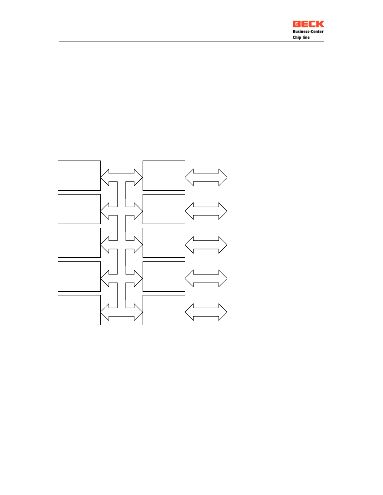
The IPC@CHIP family microcontrollers also integrates the functions of the CPU, multiplexed
address bus, three timers, watchdog timer, chip selects, interrupt controller, two DMA controllers, two
asynchronous serial ports, and programmable I/O (PIO) pins on one chip.
The @CHIP SC12 microcontroller is a highly integrated design that provides all Media Access Control
(MAC) and Encode-Decode (ENDEC) functions in accordance with the IEEE 802.3 standard. Network
interfaces including 10Base-T via the Twisted-pair. The integrated 10Base-T transceiver makes
@Chip SC12 more cost-effective.
Compared to the 80C186/188 microcontrollers, the IPC@CHIP family microcontrollers
enables designers to reduce the size, power consumption, and cost of embedded systems, while
increasing reliability, functionality, and performance.
The IPC@CHIP family microcontrollers has been designed to meet the most common requirements
of embedded products developed for the communications, office automation, mass storage, and
general embedded markets. Specific applications including industrial controls, data collection, protocol
conversion, process monitoring and internet connectivity.
IPC@CHIP family microcontroller block diagram
DRAM
256Kx16
CPU
80186
80188
Ethernet
PHY
Flash
512Kx8
DMA
UAR
T
CORE
LOGIC
WATCH
DOG
8 Bit Address-/Databus
AD[0..7], ALE
A[0..2], RD#, WR#
INT[0,2..6], INTA#
10Base-
T
T
PTX+, TPTX-
T
PRX+, TPRX-
Link/
T
raffic LED
T
xD[0..1], RxD[0..1]
CTS[0..1], RTS[0..1]
DRQ[0..1]
Pro
g
rammable I/O
PIO[0..13]
PCS[0..3,5..6]
T
MRIN[0..1]
T
MROUT[0..1]
RESET#, NMI
Ethernet
MAC
Oscilator
20MHz
The Function of I²C is realised with Programmable I/O Pins.
Access to hardware components over API functions.
Page 5
IPC@CHIP - SC12
Hardware Manual v1.1 [05.11.2002]
©BECK IPC GmbH page 5 of 28
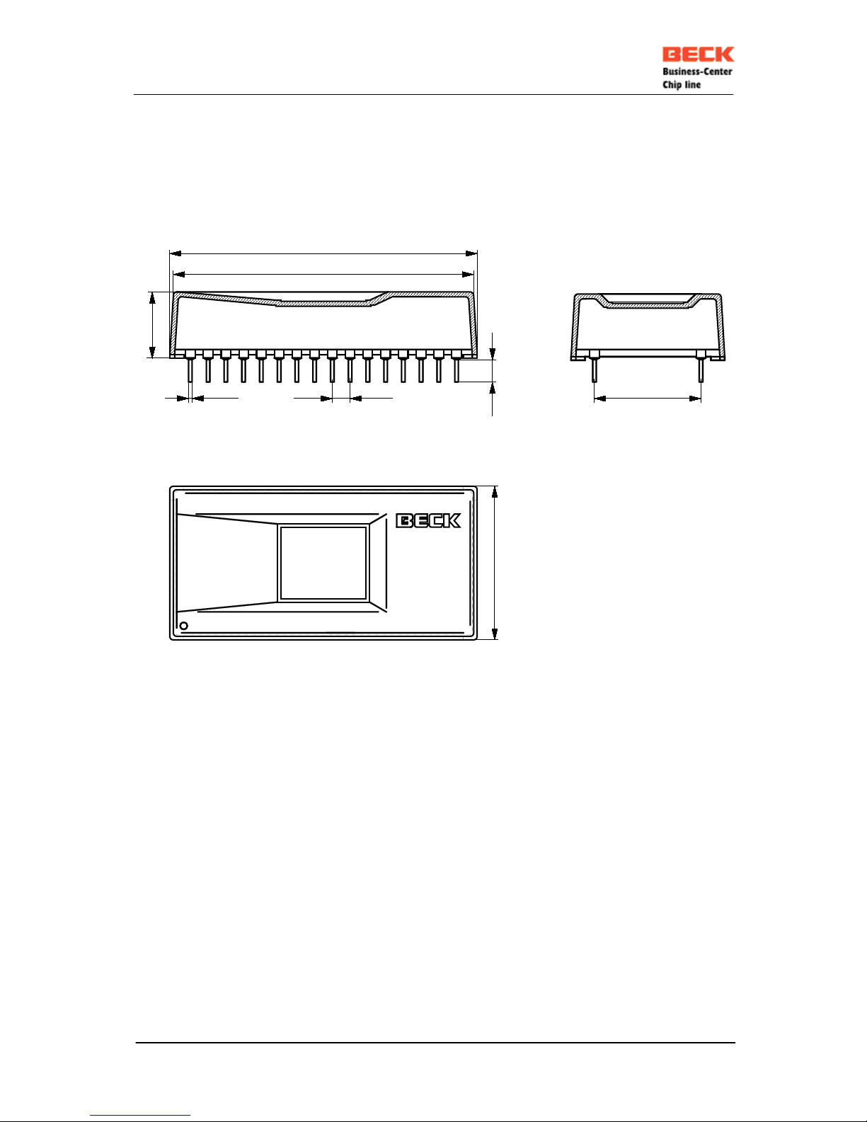
2. PHYSICAL DIMENSIONS
9
,
5
44,0
43,0
IPC@CHIP
12A9912b
GERMANY
2
2
,
0
2,54 15,24
0,5
3
,
0
Page 6
IPC@CHIP - SC12
Hardware Manual v1.1 [05.11.2002]
©BECK IPC GmbH page 6 of 28
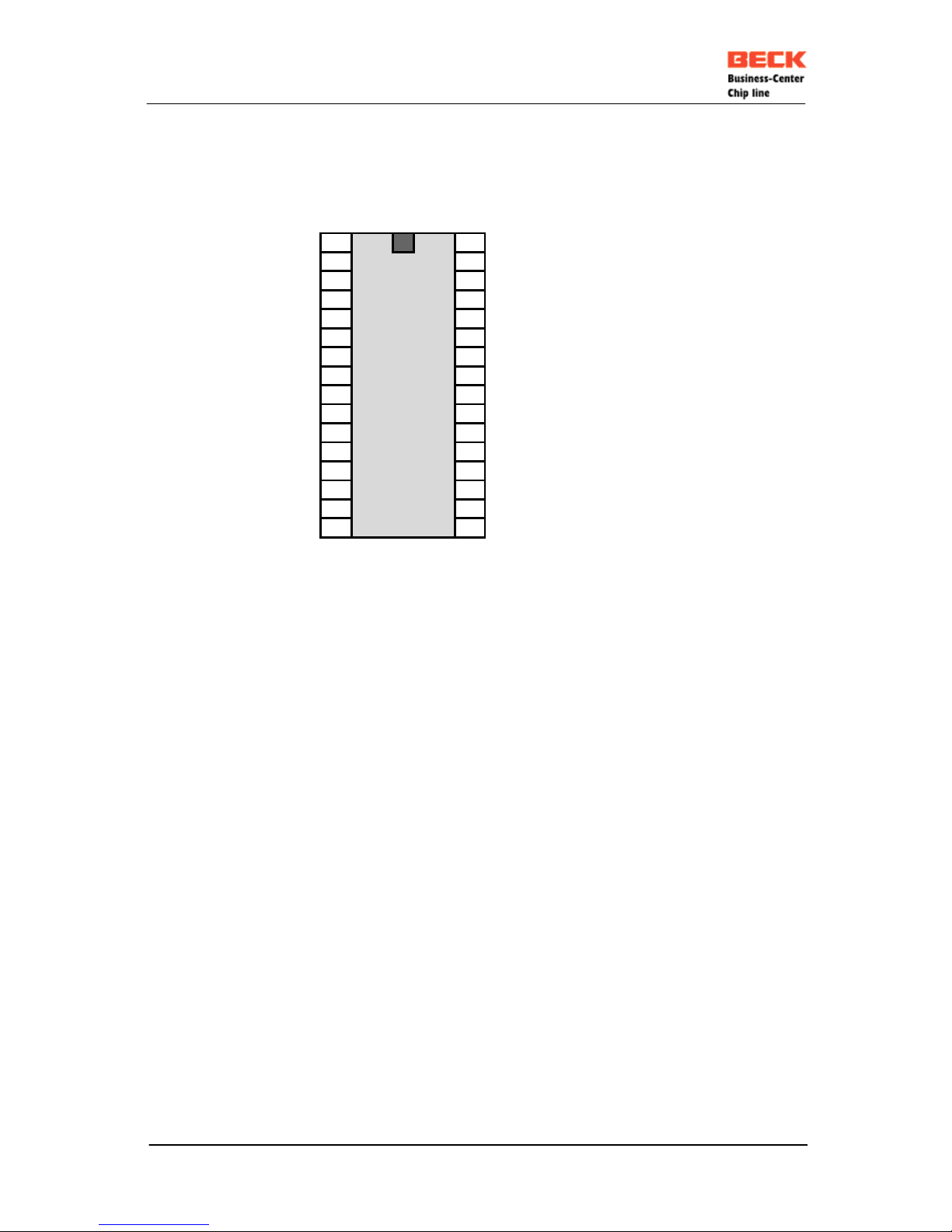
3. PIN CONFIGURATION
PIO7 / RXD0
1 32
VCC
PIO8 / TXD0
2 31
(I2C_SCL)* / DRQ1 / INT6 / PIO0
PIO9 / CTS0
3 30
(I2C_SDA)* / DRQ0 / INT5 / PIO1
PIO10 / RTS0
4 29
A2 / PCS6# / PIO2
PIO11 / TXD1
5 28
A1 / PCS5# / TMRIN1 / TMROUT1 / PIO3
PIO12 / INT3 / RXD1
6
IPC@CHIP
27
A0 / PCS1# / TMRIN0 / PIO4
PIO13 / INT0 / TMROUT0
7 26
RTS1 / PCS3# / INT4 / PIO5
AD0
8 25
CTS1 / PCS2# / INT2 / PWD / INTA# / PIO6
AD1
9 24
ALE / PCS0#
AD2
10 23
WR#
AD3
11 22
RD#
AD4
12 21
TPRX-
AD5
13 20
TPRX+
AD6
14 19
TPTX-
AD7
15 18
TPTX+
GND
16 17
RESET# / NMI / LINK_LED
* any other PIO pin may be assigned for use I²C signal by software
Locate decoupling capacitors as close to VCC Pin as physically possible.
Page 7

IPC@CHIP - SC12
Hardware Manual v1.1 [05.11.2002]
©BECK IPC GmbH page 7 of 28
4. PIN FUNCTIONS
Pin Terminology
The following terms are used to describe the pins:
Input (I) - An input-only pin.
Input (IS) - An input-only pin with Schmitt Trigger.
Output (O) - An output-only pin.
Input/Output (I/O) - A pin that can be either input or output.
4.1 Address / Data bus
Pin Name Type Function
A[0..2] O
Address Bus (output, three-state)
These pins supply nonmultiplexed memory or I/O addresses to the system.
During a bus hold or reset condition, the address bus is in a highimpedance state.
A0–A2 will serve as the nonmultiplexed address bus for external
peripherals. A0-A2 covers an address range of 8 Byte max.
AD[0..7] I/O
Multiplexed Address and Data Bus (input/output, three-state, levelsensitive)
These time-multiplexed pins supply partial memory or I/O addresses, as
well as data, to the system. This bus supplies the low-order 8 bits of an
address to the system during the first period of a bus cycle (t1), and it
supplies data to the system during the remaining periods of that cycle (t2 ,
t3 , and t4). In 8-bit mode, AD7–AD0 supplies the data for both high and low
bytes.
During a bus hold or reset condition, the address and data bus is in a highimpedance state.
ALE O
Address Latch Enable (output)
This pin indicates to the system that an address appears on the address
and data bus (AD7–AD0). The address is guaranteed to be valid on the
trailing edge of ALE.
ALE is three-stated and held resistively Low during a bus hold condition. In
addition, ALE has a weak internal pulldown resistor that is active during
reset, when it is enabled by software.
RD# O
Read Strobe (output, three-state)
This pin indicates to the system that the microcontroller is performing a
memory or I/O read cycle. RD is guaranteed to not be asserted before the
address and data bus is floated during the address-to-data transition. RD
floats during a bus hold condition.
WR# O
Write Strobe (output)
This pin indicates to the system that the data on the bus is to be written to a
memory or I/O device. WR floats during a bus hold or reset condition.
Page 8
IPC@CHIP - SC12
Hardware Manual v1.1 [05.11.2002]
©BECK IPC GmbH page 8 of 28
4.2 Programmable I/O Pins
Pin Name
Type Function
PIO[0..13] I/O
Programmable I/O Pins (input/output, open-drain)
The IPC@CHIP family microcontroller provides 14 individually
programmable I/O pins. Each PIO can be programmed with the
following attributes: PIO function (enabled/disabled), direction
(input/output), and weak pullup or pulldown.
PIO# After power-on reset, the PIO pin
defaults to
Programmable as
Input with
0 Input without pullup
1 Input without pullup
2 Input with pullup pullup
3 Input with pullup pullup / pulldown
4 Input with pullup pullup
5 Input with pullup pullup
6 Input with pullup pullup
7 RxD0 pullup
8 TxD0 pullup
9 Input with pullup pullup
10 Input with pullup pullup
11 TxD1 pullup
12 RxD1 pullup
13 Input with pulldown Pulldown
Internal Pullup and Pulldown is approximately 10kOhm.
Page 9

IPC@CHIP - SC12
Hardware Manual v1.1 [05.11.2002]
©BECK IPC GmbH page 9 of 28
4.3 Programmable Chip Selects
Pin Name Type Function
PCS[0..3] O
Peripheral Chip Selects (output)
These pins indicate to the system that an I/O memory access is in
progress to the corresponding region of the peripheral memory.
PCS0–PCS3 are three-stated and held resistively High during a bus
hold condition. In addition, PCS0–PCS3 each have a weak internal
pullup resistor that is active during reset. The PCS outputs assert with
the multiplexed AD address bus. Note also that each peripheral chip
select asserts over a 256-byte address range. PCS0–PCS3 have
extended wait state options, active for at least 800ns.
PCS[5..6] O
Peripheral Chip Selects (output)
These pins indicate to the system that an I/O memory access is in
progress to the corresponding region of the peripheral memory.
PCS5–PCS6 are three-stated and held resistively High during a bus
hold condition. In addition, PCS5–PCS6 each have a weak internal
pullup resistor that is active during reset. The PCS outputs assert with
the multiplexed AD address bus. Note also that each peripheral chip
select asserts over a 256-byte address range. PCS5–PCS6 also have
wait state, active for at least 150ns.
4.4 Interrupts
Pin Name Type Function
INT[0,2-6] I
Maskable Interrupt Request (input)
These pins indicate to the microcontroller that an interrupt request has
occurred. If the INT pin is not masked, the microcontroller transfers program
execution to the location specified by the corresponding INT vector in the
microcontroller interrupt vector table.
Interrupt requests are synchronized internally and can be edge-triggered or
level-triggered. To guarantee interrupt recognition, the requesting device
must continue asserting INT until the request is acknowledged. INT2
becomes INTA# when INT0 is configured in cascade mode. *
INTA# * O
Interrupt Acknowledge (output)
When the microcontroller interrupt control unit is operating in cascade
mode, this pin indicates to the system that the microcontroller needs an
interrupt type to process the interrupt request on INT0. The peripheral
issuing the interrupt request must provide the microcontroller with the
corresponding interrupt type.
PWD IS
Pulse Width Demodulator (input, Schmitt trigger)
If pulse width demodulation is enabled, PWD processes the signal through
a Schmitt trigger. PWD is used internally to drive TMRIN0 and INT2, and
PWD is inverted internally to drive TIMERIN1 and INT4. If INT2 and INT4
are enabled and timer 0 and timer 1 are properly configured, the pulse width
of the alternating PWD signal can be calculated by comparing the values in
timer 0 and timer 1.
In PWD mode, the signals TMRIN0, TMRIN1 and INT4 can be used as
PIOs. If they are not used as PIOs, they are ignored internally.
* currently not supported by software
Page 10

IPC@CHIP - SC12
Hardware Manual v1.1 [05.11.2002]
©BECK IPC GmbH page 10 of 28
4.5 Timer
Timer can be clocked internally or externally. Maximum frequency is 5MHz. If timer will be clocked
internally timer out pin (TMROUT) may be used. External clock at Input and output at the same time
with same timer is not possible.
Pin Name Type Function
TMRIN[0..1] I
Timer Input (input, edge-sensitive)
These pins supply a clock or control signal to the internal microcontroller
timer 0 and 1. After internally synchronizing a Low-to-High transition on
TMRIN, the microcontroller increments the corresponding timer. TMRIN
must be tied High if not being used. When PIO is enabled, TMRIN is pulled
High internally.
TMRIN0 is driven internally by INT2/PWD when pulse width demodulation
mode is enabled. The TMRIN0 pin can be used as a PIO when pulse width
demodulation mode is enabled.
TMROUT[0..1] O
Timer Output (output)
These pins supplies the system with either a single pulse or a continuous
waveform with a programmable duty cycle. TMROUT is floated during a bus
hold or reset.
4.6 10Base-T Interface
Pin Name Type Function
TPTX[+,-] O
Twisted Pair Driver (outputs)
These two outputs provide the TP drivers with pre-distortion capability
TPRX[+,-] I
Twisted Pair Receive (inputs).
A differential receiver tied to the receive transformer pair of the twisted-pair
wire.
The receive pair of the twisted-pair medium is driven with 10 Mbits/s
Manchester-encoded data
LINK LED O
Link and Traffic LED Driver (output)
If TP is LINK-pass, this pin outputs 3V in sink-mode.
This pin will output 5V, generated as an open-collector Hi mode for 50ms to
indicate the presence of traffic on the network. Note that this pin is not able
to source any current !
Please refer also to the schematic in chapter 10.2 Link LED / RESET.
4.7 Asynchronous Serial Ports
All asynchronous port pins are TTL level. To provide RS232 or RS485 level external drivers must be
connected (like MAX232). Following modes can be provided:
Full-Duplex Operation with 7-bit or 8-bit, odd, even or no parity. Error detection is possible with parity
errors, framing errors, overrun errors and break character recognition. Hardware handshaking (Clearto-send CTS and Request-to-send RTS) is possible.
To get a definite baud rate a baud rate divider must be provided.
A general formula for the baud rate divisor is:
BAUDDIV = (20 000 000 / (16 x Baud Rate))
The maximum baud rate is achieved by setting BAUDDIV=0001h. This results in a baud rate of
1250 Kbit. A BAUDDIV setting of zero results in no transmission or reception of data.
The serial port receiver can tolerate a 3.0% overspeed and 2.5% underspeed baud rate deviance.
The two ports can operate at different rates.
Page 11

IPC@CHIP - SC12
Hardware Manual v1.1 [05.11.2002]
©BECK IPC GmbH page 11 of 28
Pin Name Type Function
TxD[0..1] O
Transmit Data (output)
These pins supply asynchronous serial transmit data to the system from
serial port 0 and 1.
RxD[0..1] I
Receive Data (input)
These pins supply asynchronous serial receive data from the system to
asynchronous serial ports 0 and 1.
CTS[0..1] I
Clear-to-Send (input)
These pins provide the Clear-to-Send signal for asynchronous serial port 0
and 1 when hardware flow control is enabled for the port. The CTS signals
gate the transmission of data from the associated serial port transmit
register. When CTS is asserted, the transmitter begins transmission of a
frame of data, if any is available. If CTS is deasserted, the transmitter holds
the data in the serial port transmit register. The value of CTS is checked
only at the beginning of the transmission of the frame.
RTS[0..1] O
Request-to-Send 0 (output)
These pins provide the Request-to-Send signal for asynchronous serial
ports 0 and 1 when hardware flow control is enabled for the port. The RTS
signals are asserted when the associated serial port transmit register
contains data that has not been transmitted.
4.8 DMA
Pin Name Type Function
DRQ[0..1] I
DMA Request (input, level-sensitive)
These pins indicate to the microcontroller that an external device is ready
for DMA channel 0 or 1 to perform a transfer. DRQ0 is edge-triggered and
internally synchronized. DRQ is not latched and must remain active until
serviced.
Page 12
IPC@CHIP - SC12
Hardware Manual v1.1 [05.11.2002]
©BECK IPC GmbH page 12 of 28
4.9 I2C-Bus
The IPC@CHIP family microcontroller handles up to 127 external slaves. It is always master. Slave
mode is not implemented.
I²C is implemented by software emulation. Maximum Frequency is about 30 kHz without longer breaks
by interrupt. External pullups are necessary.
Pin Name Type Function
I2C_SCL O
I2C-Bus Clock (output)
This pin provides clock to an external I2C slave by default. Any other PIO pin
may be assigned for use as I
2
C_SCL signal by software.
I2C_SDA I/O
I2C-Bus Data in/out (input/output)
This pin acts either as data input or data output as defined by the I2C protocol
convention. Any other PIO pin may be assigned for use as I
2
C_DAT signal by
software.
4.10 Reset, Power Fail Generator
Note that RESET# pin shares 4 functions: RESET and NMI as described here, as well as network link
state and network traffic as described in the corresponding chapters.
This is a voltage-multiplexed pin that internally sinks current only in case of internally generated reset
or NMI condition. All peripheral logic asserted to this pin must be open-collector to prevent the internal
logic from sinking too high current. It is provided with 1kOhm Pullup.
Pin Name Type Function
RESET# I/O
Reset (input/level-sensitive)
If voltage on this pin goes below 0.8V the microcontroller will perform a reset.
In that case the microcontroller immediately terminates its present activity,
clears it’s internal logic, and transfers CPU control to the reset address,
FFFF0h.
If Vcc goes down below 4.65V or the internal watchdog is triggered this pin will
be driven to GND internally.
NMI I
Nonmaskable Interrupt (input, level-sensitive)
If voltage on this pin goes down below 1.5V it indicates to the microcontroller
that an interrupt request has occurred. The NMI signal is the highest priority
hardware interrupt and, unlike the INT6–INT0 pins, cannot be masked. The
microcontroller always transfers program execution to the location specified by
the nonmaskable interrupt vector in the microcontroller interrupt vector table
when NMI is asserted.
Although NMI is the highest priority interrupt source, it does not participate in
the priority resolution process of the maskable interrupts.
There is no bit associated with NMI in the interrupt in-service or interrupt
request registers. This means that a new NMI request can interrupt an
executing NMI interrupt service routine. As with all hardware interrupts, the IF
(interrupt flag) is cleared when the processor takes the interrupt, disabling the
maskable interrupt sources. However, if maskable interrupts are re-enabled by
software in the NMI interrupt service routine, via the STI instruction for
example, the fact that an NMI is currently in service does not have any effect
on the priority resolution of maskable interrupt requests. For this reason, it is
strongly advised that the interrupt service routine for NMI should not enable the
maskable interrupts. An NMI transition from Low to High is latched and
synchronized internally, and it initiates the interrupt at the next instruction
boundary. To guarantee that the interrupt is recognized, the NMI condition
must be asserted to the pin for at least one CLK period.
Page 13

IPC@CHIP - SC12
Hardware Manual v1.1 [05.11.2002]
©BECK IPC GmbH page 13 of 28
Pin Name Type Function
The NMI is for detecting low supply power and the following data backup only.
A reset has to follow after the NMI.
At turn-on the IPC@Chip I/O pins are configured as follows:
Pin1: RXD0/PIO7 = RXD0
Pin2: TXD0/PIO8 = TXD0
Pin3: CTS0/PIO9 = Input pullup
Pin4: RTS0/PIO10 = Input pullup
Pin5: TXD1/PIO11 = TXD1
Pin6: RXD1/PIO12 = RXD1
Pin7: TMROUT0/INT0/PIO13 = Input pulldown
Pin17: RESET/PFAIL/LILED = Input
Pin24: ALE/PCS0 = Output, value 1
Pin25: CTS1/PCS2/PIO6/INT2 = Input pullup
Pin26: RTS1/PCS3/PIO5/INT4 = Input pullup
Pin27: PCS1/PIO4/TMRIN0/A0 = Input pullup
Pin28: PCS5/PIO3/TMROUT1/TMRIN1/A1 = Input pullup
Pin29: PCS6/PIO2/A2 = Input pullup
Pin30: I2CDAT/INT5/PIO1 = Input
Pin31: I2CCLK/INT6/PIO0 = Input
Page 14
IPC@CHIP - SC12
Hardware Manual v1.1 [05.11.2002]
©BECK IPC GmbH page 14 of 28
VCC
(V)
5
4
3
2
1
200 400 600 800 1000 1200 1400 1600
t
REM
t
on/off
(ms)
t
Power OK
t
REM
=Time to save the retentive data
e. g. 1 kByte = 120 ms
2 kByte = 200 ms
t
Power OK
= max. 200 ms
VCC
(V)
5
4
3
2
1
200 400 600 800 1000 1200 1400 1600
t
on/off
(ms)
Power up & power down sequence
4,7 V
5 V
NMI reset LILED sequence
4,65 V
t
REM
1,4 V
0,8 V
RESET
NMI
LINK
LINK
80 ms Link pause
3,0 V
Traffic
50 ms traffic imp.
0,8 V
To realize time to save the retentive data keep Pin 17 above 0,8V for t
REM
with external capacitors. If
Pin 17 goes below 0,8V IPC@CHIP will be in reset state.
If VCC goes below 4,65V IPC@CHIP will be in reset state and Pin 17 goes below 1,3V until Voltage
comes back.
Note: Retentive data must be one block.
If it is not, it takes more time to save.
Page 15
IPC@CHIP - SC12
Hardware Manual v1.1 [05.11.2002]
©BECK IPC GmbH page 15 of 28
5. MUTUAL EXCLUSIVE FUNCTIONS
The IPC@CHIP family microcontroller provides a lot of different functions by several multi-function
pins. Choosing one function will result in disabling other functions. The following table shows, which
functions are mutual exclusive.
Pin Name Function Exclusion
A0 nonmultiplexed address A0 PIO4, PCS1#, TMRIN0
A[1..2] nonmultiplexed address
A[1..2]
PIO[2..3], PCS[5..6], Timer 1
ALE Address / Data bus PCS0#
CTS0 hardware flow control Serial
Port 0
PIO9
CTS1 hardware flow control Serial
Port 1
PIO6, PCS2#, INT2, INTA#, PWD
DRQ0 DMA Request 0 PIO1, INT5, I2C-Bus
DRQ1 DMA Request 1 PIO0, INT6, I2C-Bus
I2C_SCL,
I
2
C_SDA
I2C-Bus by default PIO[0..1], DMA, INT[5..6]
By default pin-assignment of the I2C functions is in
conflict with these pin functions, but the user is free to
assign the I
2
C functions to any other PIO pin,
disabling the other functions of the pin chosen.
INT0 Interrupt Request 0 PIO13, TMROUT0, cascaded Interrupt Controller *
INT2 Interrupt Request 2 PIO6, PCS2#, INTA#, PWD, hardware flow control
Serial Port 1
INT3 Interrupt Request 3 PIO12, Serial Port 1
INT4 Interrupt Request 4 PIO5, PCS3#, SPI, hardware flow control Serial Port 1
INT5 Interrupt Request 5 PIO1, DRQ0, I2C-Bus
INT6 Interrupt Request 6 PIO0, DRQ1, I2C-Bus
INTA# * cascaded Interrupt Controller PIO6, PIO13, INT0, INT2, PCS2#, PWD, TMROUT0,
hw flow control Serial Port 1
PWD Pulse Width Demodulator PIO6, PCS2, INT2, INT4, TMROUT[0..1],
TMRIN[0..1], INTA#, cascaded Interrupt Controller *,
hw flow control Serial Port 1
PCS0# programmable chip select 0 Address/Data bus
PCS1# programmable chip select 1 A0, PIO4, TMRIN0
PCS2# programmable chip select 2 PIO6, INT2, INTA#, PWD, hw flow control Serial Port
1, cascaded Interrupt Controller *
PCS3# programmable chip select 3 PIO5, INT4, hardware flow control Serial Port 1
PCS5# programmable chip select 5 A[1..2], PIO3, Timer 1
PCS6# programmable chip select 6 A[1..2], PIO2
PIO0 Programmable I/O DRQ1, INT6, I2C-Bus
PIO1 Programmable I/O DRQ0, INT5, I2C-Bus
PIO2 Programmable I/O A2, PCS6#
PIO3 Programmable I/O A1, PCS#, Timer 1
PIO4 Programmable I/O A0, PCS1#, TMRIN0
PIO5 Programmable I/O PCS3#, INT4, hardware flow control Serial Port 1
PIO6 Programmable I/O PCS2#, INT2, cascaded Interrupt Controller *, PWD,
hw flow control Serial Port 1
PIO7 Programmable I/O Serial Port 0
PIO8 Programmable I/O Serial Port 0
PIO9 Programmable I/O Hardware flow control Serial Port 0
PI1O Programmable I/O Hardware flow control Serial Port 0
Page 16

IPC@CHIP - SC12
Hardware Manual v1.1 [05.11.2002]
©BECK IPC GmbH page 16 of 28
Pin Name Function Exclusion
PI11 Programmable I/O Serial Port 1
PI12 Programmable I/O Serial Port 1, INT3
PI13 Programmable I/O INT0, cascaded Interrupt Controller *, TMROUT0
RxD0, TxD0 Serial Port 0 w/o hw flow
control
PIO[7..8]
RxD0, TxD0
CTS0, RTS0
Serial Port 0 with hw flow
control
PIO[7..10]
RxD1, TxD1 Serial Port 1 w/o
hw flow control
PIO[11..12], INT3
RxD1, TxD1
CTS1, RTS1
Serial Port 1 with hw flow
control
PIO[5..6,11..12], INT3, PCS[2..3]#, INT2, INT4, PWD,
cascaded Interrupt Controller *
* currently not supported by software
Page 17
IPC@CHIP - SC12
Hardware Manual v1.1 [05.11.2002]
©BECK IPC GmbH page 17 of 28
6. ETHERNET 10BASE-T
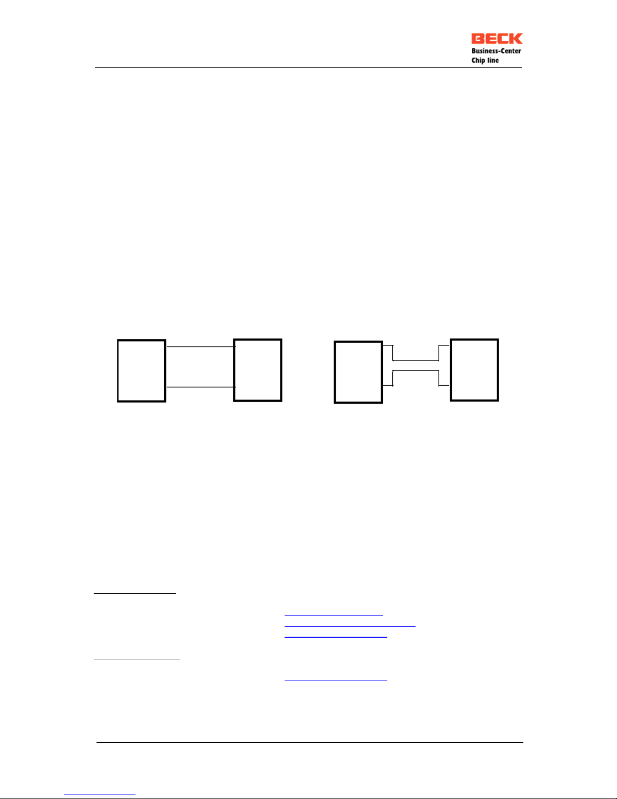
6.1 10Base-T Media Filter Placement and Termination
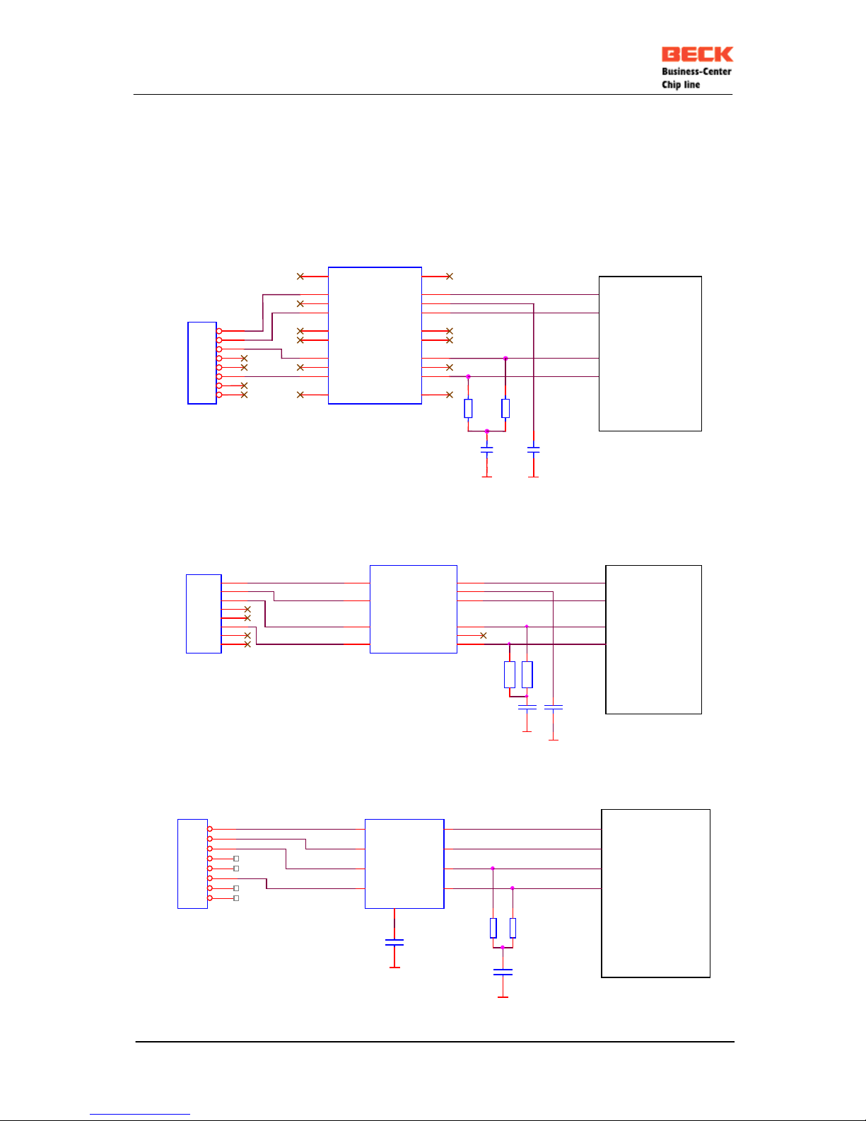
Placement of the termination components TPTX+ and TPTX- should be located as physically close to
the media filter as possible.
The media filter should also placed as physically close to the RJ-45 connector as possible to minimize
stray EMI transfer to the media. The trace routing is to keep the area enclosed by a circuit loop as
small as possible to minimize the incidence of magnetic coupling. However this can conflict with the
general rule of keeping trace lengths to a minimum. For example, if circuit components are positions
along the same sides of a square, the best return is back along the same three sides of the square,
NOT directly back along the fourths side. This rule must be strictly adhered to. Furthermore, there
should never be an unnecessary via feed-through inside the circuit loop. This also implies that the
circuit loop should never encircle the power/ground planes (i.e., part of the circuit loop above and part
of circuit loop below this planes).
Incorrect Layout
Correct Layout
The two traces of the pair should always be routed in adjacent channels and should be of same
length. To reduce capacitive coupling, each circuit loop should be separated from the others. Circuit
loops can be separated either by physical space (if located on the same layer) or by placement on
signal layers on the opposite side of the power/ground planes. The following signal groups should be
isolated from each other. Width of receiver trace should be 25 mil minimum to achieve 50Ohm
impedance characteristic at 10MHz. Width of transmitter trace should be 10 mil minimum to achieve
25Ohm impedance characteristic at 10MHz
To achieve optimum performance the designer must protect the magnetics from the environment. It
should be isolated from the power and ground planes.
6.2 Magnetics approved for use for 10Base-T application
Through-Hole PCB:
BEL FUSE, Inc. part no. 0556-5999-19 (http://www.belfuse.com)
Halo Electronics, Inc. Part no. FS22-101Y4 (http://www.haloelectronics.com)
Valor, Inc. part no. FL1012/1066 (http://www.valorinc.com/)
Surface-Mount PCB:
Valor, Inc. part no. SF1012 (http://www.valorinc.com/)
Page 18
IPC@CHIP - SC12
Hardware Manual v1.1 [05.11.2002]
©BECK IPC GmbH page 18 of 28
7. SYSTEM OVERVIEW
IPC@CHIP family microcontroller has a system configuration based on the ISA architecture with
some changes: No ISA-Bus, no Video-Interface, no Keyboard Interface, programming of Serial Ports,
DMA, PIC and Timer is different from standard IBM PC.
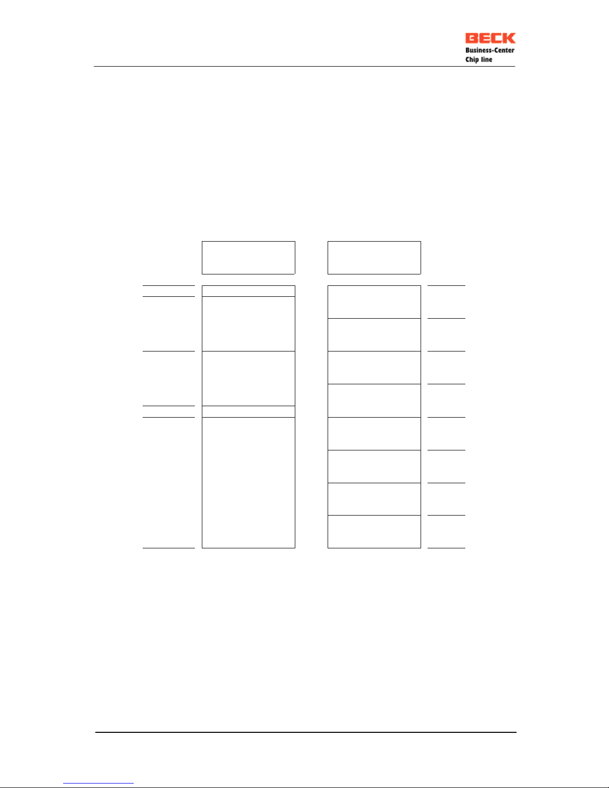
This section provides an overview of the system memory configuration and basic I/O.
7.1 Memory map
SC12 Memory I/0 map
FFFFFh
Bootloader
FFFFh
FEFFFh
Reserved
0700h
Flash Disk
06FFh
PCS6#
XXXXXh* 0600h
XXXXXh* 05FFh
PCS5#
@CHIP RTOS
0500h
04FFh
80400h
Reserved
80000h
Reserved
0400h
7FFFFh 03FFh
PCS3#
0300h
02FFh
PCS2#
Working Memory
0200h
512Kbyte RAM
01FFh
PCS1#
0100h
00FFh
PCS0#
00000h 0000h
* depends on the BIOS version
Page 19

IPC@CHIP - SC12
Hardware Manual v1.1 [05.11.2002]
©BECK IPC GmbH page 19 of 28
7.2 System interrupts
Number of Interrupt
Source Sensitivity
0 = INT0 (external) Edge / Level
1 = Network controller (internal)
2 = INT2 (external) Edge / Level
3 = INT3 (external) Edge / Level
4 = INT4 (external) Edge / Level
5 = INT5 (external) Edge
6 = INT6 (external) Edge
7 = Reserved
8 = Timer0 (internal)
9 = Timer1 (internal)
10 = Timer 1ms (internal) (*)
11 = Serial port 0 (internal) (*)
12 = Serial port 1 (internal) (*)
13 = Terminal count DMA channel 0 (internal) (*)
14 = Terminal count DMA channel 1 (internal) (*)
15 = NMI (internal/external)
(*) = Currently not supported
Since an interrupt occurs all interrupts are disabled until the interrupts are released by setting IF Flag
in interrupt service routine. Interrupts of the same source are masked until the corresponding Bit in
interrupt service register is cleared.
Level sensitiv interrupts are caused by high level, edge sensitiv interrupts by the rising edge.
7.3 Watchdog
The build in watchdog prevent the SC12 to lead to an unexpected fail mode in software and hardware.
The watchdog timeout period is about 838 ms. The mode can set to trigger the watchdog by user
programm or by the BIOS (default). In BIOS mode, the BIOS performs the watchdog strobing provided
that the system's timer interrupt is allowed to execute. Beware that excessive interrupt masking
periods can lead to system resets.
Page 20

IPC@CHIP - SC12
Hardware Manual v1.1 [05.11.2002]
©BECK IPC GmbH page 20 of 28
8. CHARACTERISTICS
8.1 ABSOLUTE MAXIMUM RATINGS
Storage temperature : -55°C to +125°C see IEC 68-2-1/2
Supply voltage (Vcc) : -0.3V to +6.0V
Supply current (Vcc = 5,25V) : 300 mA
Voltage on any pin with respect to ground : -0.3V to Vcc + 0.3V
8.2 OPERATING RANGES
Operating temperature (Case temp. tc) : 0°C to +55°C
Supply voltage (Vcc) : 5.0V +/- 5%
Power supply current @ 20MHz (5,25V): typ. 200mA max. 300mA
8.3 DC-CHARACTERISTICS
Symbol Parameter Test Condition Value Preliminary Unit
Description MIN. TYP. MAX.
VOL Voltage Output Low IOL = 2.0mA - 0.45 V
VOH Voltage Output High IOH = -0.4mA 2.4 - V
V
VILO Voltage Input Low - - 0.8 V
VIHI Voltage Input High - 2.0 - V
VRT Reset Threshold 4.5 4.65 4.75 V
Reset Threshold
Hysteresis
0.4 V
VRESL
O
IN Voltage Reset active 0.8 V
VRESHI IN Voltage Reset inactive 2.0 V
VRESO
L
OUT Voltage Reset Low IOL = 1.2mA 0.4 V
VRESO
H
OUT Voltage Reset High IOH = -0.8mA Vcc-1.5 V
VNMIRT NMI Threshold VCC = 5V 1.3 1.4 1.5 V
INMI NMI Input Current
VTIDF Voltage TP Input 0.35 2.0 V
VTIL Voltage TP Output Low 0.8 V
VTIH Voltage TP Output High 2.4 V
Clout External Load on AD[0..7],
RD#, WR#
20 PF
External Load on the other
pins
30 PF
Clin Input Capacitance 30 PF
Page 21
IPC@CHIP - SC12
Hardware Manual v1.1 [05.11.2002]
©BECK IPC GmbH page 21 of 28
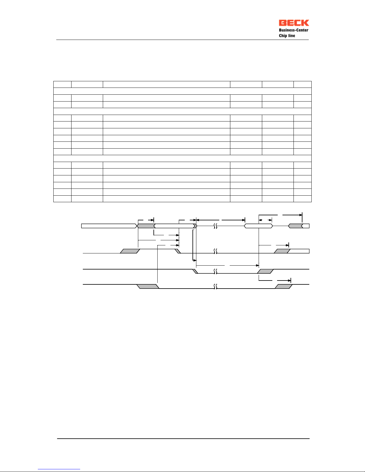
8.4 AC-CHARACTERISTICS
8.4.1 Read Cycle
No. Symbol Description Min Max Unit
General Timing Requirements
1 t
RLDV
Read Valid to Data Valid – PCS0#..PCS3# Active 820 ns
1 t
RLDV
Read Valid to Data Valid – PCS5#, PCS6# Active 220 ns
General Timing Responses
10 t
LHLL
ALE Width 40 ns
12 t
AVLL
AD Address Valid to ALE Low 23 ns
13 t
LLAX
AD Address Hold from ALE Inactive 23 ns
17 t
CXCSX
PCSx# Hold from Read Inactive 23 ns
23 t
LHAV
ALE High to Address Valid 20 ns
99 t
PLAL
PCSx# Active to ALE Inactive 15 28 ns
Read Cycle Timing Responses
24 t
AZRL
AD Address Float to Read Active 0 ns
26 t
RLRH
Read Pulse Width – PCS0#..PCS3# Active 835 ns
26 t
RLRH
Read Pulse Width – PCS5#, PCS6# Active 235 ns
28 t
RHLH
Read Inactive to ALE High (a) 22 ns
29 t
RHAV
Read Inactive to AD Address Active (a) 40 ns
59 t
RHDX
Read Inactive to Data Hold on AD Bus 0 ns
(a) This parameter applies to the WR# signal
Addres
s
Data
17
26
24
28
12
99
10
29
1323 1 59
AD0..AD7
ALE
RD#
PCSx#
*) the falling edge of PCS1# is 50nS delayed internaly
Page 22
IPC@CHIP - SC12
Hardware Manual v1.1 [05.11.2002]
©BECK IPC GmbH page 22 of 28
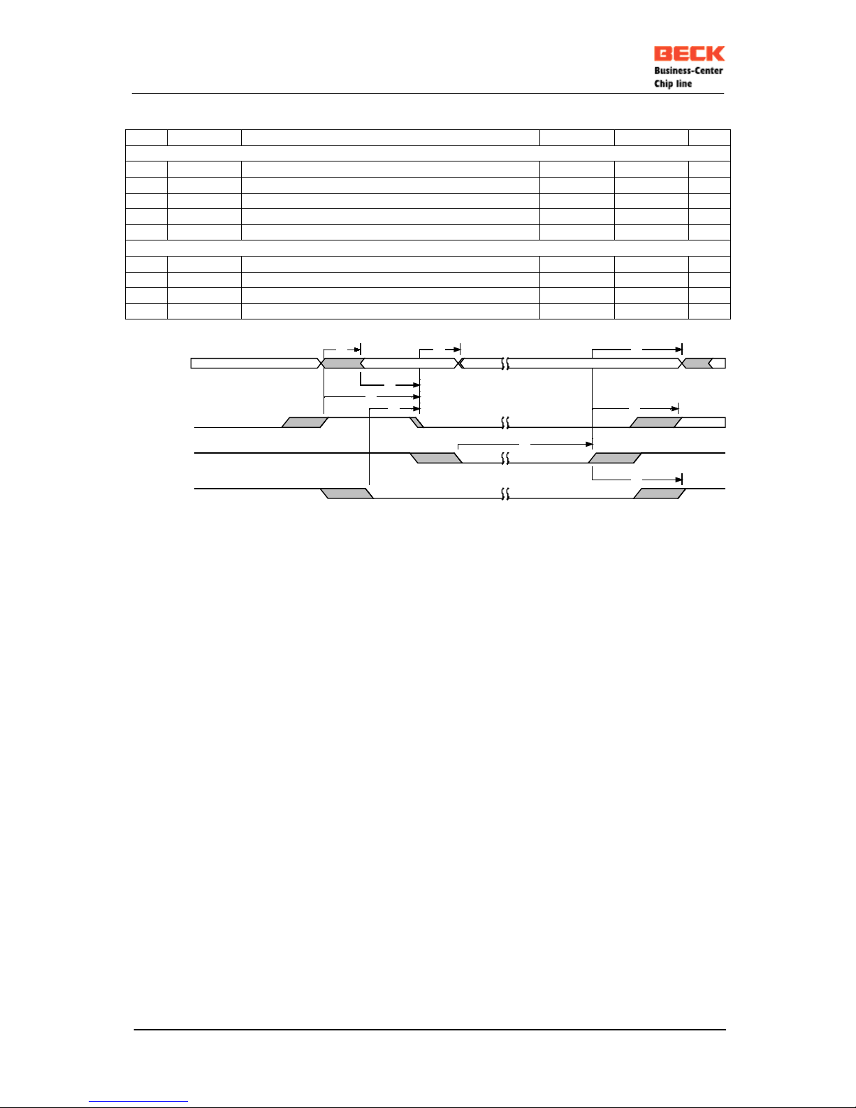
8.4.2 Write Cycle
No. Symbol Description Min Max Unit
General Timing Responses
10 t
LHLL
ALE Width 40 ns
12 t
AVLL
AD Address Valid to ALE Low 23 ns
17 T
CXCSX
PCSx# Hold from Read Inactive 23 ns
23 T
LHAV
ALE High to Address Valid 20 ns
99 T
PLAL
PCSx# Active to ALE Inactive 15 28 ns
Read Cycle Timing Responses
32 T
WLWH
Write Pulse Width - PCS0#..PCS3# Active 840 ns
32 T
WLWH
Write Pulse Width – PCS5#, PCS6# Active 240 ns
33 T
WHLH
Write Inactive to ALE High 23 ns
34 T
WHDX
Data Hold after Write Inactive 40 ns
Addres
s
Data
17
32
33
12
99
10
341323
AD0..AD7
ALE
WR#
PCSx#
*) the falling edge of PCS1# is 50nS delayed internaly
8.4.3 Interrupt Acknowledge Cycle
Currently not supported by software
Page 23

IPC@CHIP - SC12
Hardware Manual v1.1 [05.11.2002]
©BECK IPC GmbH page 23 of 28
9. ENVIRONMENTAL TEST
Following stability tests in conjunction with FEC standard are carried out (device under test
inoperative):
Dry heat and cold resistance
DIN EN60068- 2-2 Bb / 2-1 Ab
+70°C, 96h / –25°C, 96h
thermal-shock resistance
DIN IEC 60068- 2-14 Na / Nb
-25°C; +70°C / 2 cycles of 3h
Cycles with damp heat (95-100%)
DIN EN 60068– 2-30 Db
+25°C; +55°C / 2 cycles of 12h
Following stability tests are carried out independent of FEC standard:
Dry heat and cold resistance
DIN EN60068- 2-2 Bb / 2-1 Ab
+70°C, 96h / –25°C, 96h
Page 24
IPC@CHIP - SC12
Hardware Manual v1.1 [05.11.2002]
©BECK IPC GmbH page 24 of 28
10. APPLICATION EXAMPLES
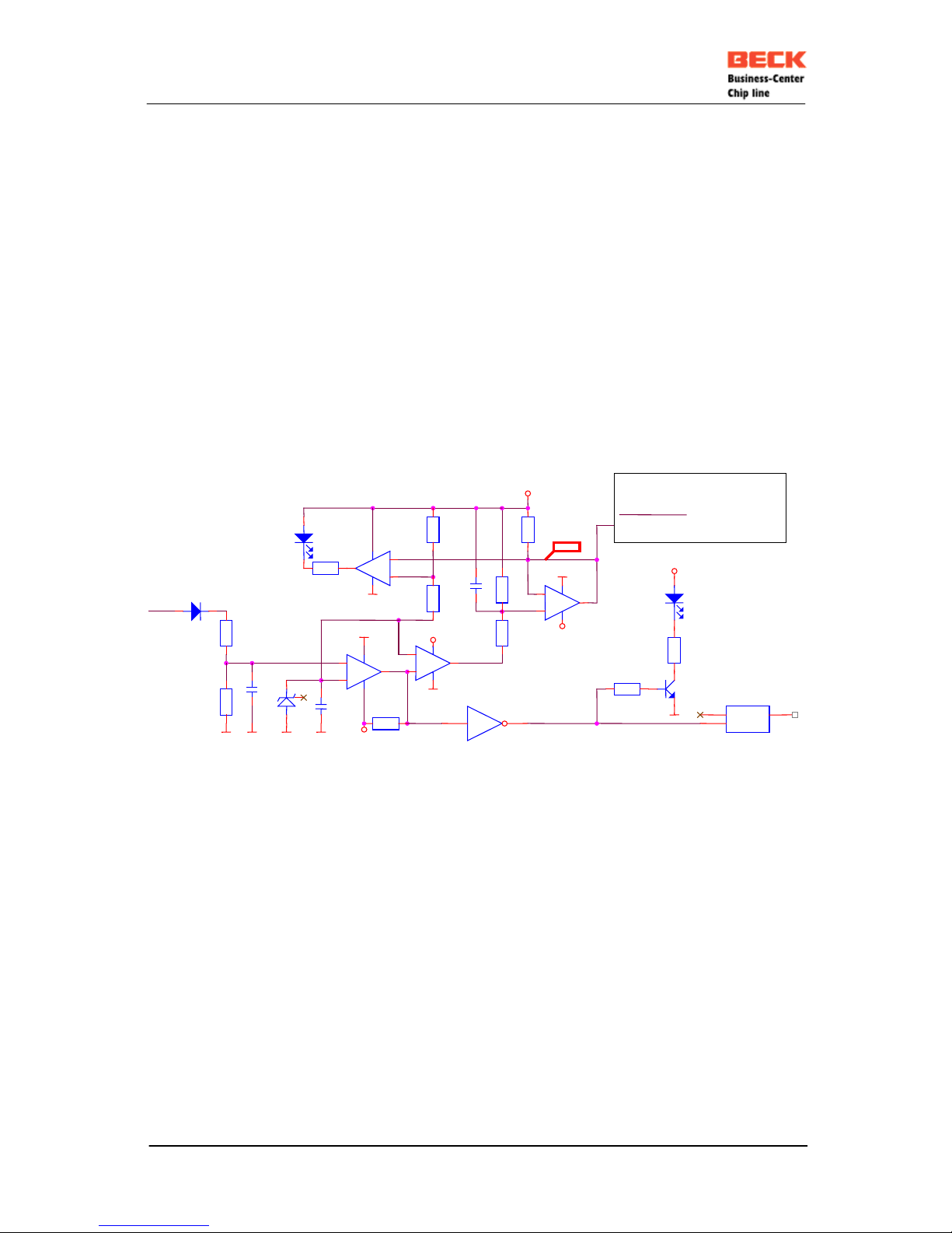
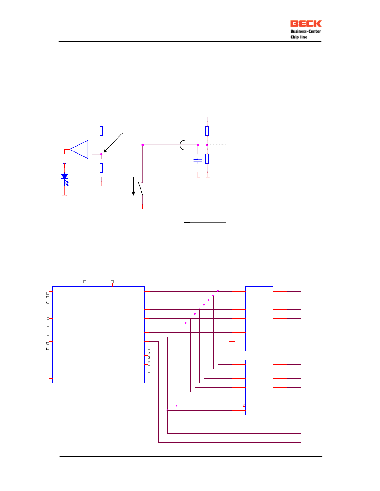
The following pages contain schematics showing the IPC@CHIP family microcontroller gives you
suggestions, how to handle the multi-function pin 17 RESET# / NMI / LINK-LED and how
to expand the SC12.
10.1 NMI / Reset-in / Link-LED
R188
R187
22k
1% !
R9
100k
The LM339 limits U17 t o
approx. 4V
+
-
IC45B
LM339
5
4
2
3
12
R147
4k7
+
-
IC45D
LM339
11
10
13
3
12
GND
VCC
C11
0.1uF
3.32V
R147 is for understanding the circuitry only. The SC12 has
already build in a 1k Ohm pullup resistor.
R182
390R
IC10B
74HCT14
3 4
External sample circuitry /Reset + NMI + Link LED
R197
27k
+
-
IC45A
LM339
7
6
1
3
12
LED1
LED3mm
R12
390R
2,5V
LED2
LED3mm
GND
R198
10k
1% !
R11
20k
INT24V
D39
LL4148
C11470p
GND
R199
22k
VCC
C64
0.1uF
Q8
BC817-25L_1
RESET#
GND
IC8
NC7S14P5X
1
2
4
NC
IN
Y
VCC
R10
680R
*
Power
GND
GND
Link
GND
+
-
IC45C
LM339
9
8
14
3
12
17
RD
1
LM385-2,5
A
K
3
330R
VCC
GND
VCC
RESET_PFAIL_LILED
SC12
GND
*
U17
*) LM339 is an open collector operational amplifier
Page 25
IPC@CHIP - SC12
Hardware Manual v1.1 [05.11.2002]
©BECK IPC GmbH page 25 of 28
10.2 Link-LED / Reset
SC12
+
-
Vcc
3,5..4
V
GND
17
GND
GND
GND
1K
RESET =
1..5mA
(static)
<
0,8
V
Vcc
GND
10.3 256x 8bit I/O-Extension using 74HCT573/245
A0
/PCS1
A6
/PCS1
/WR
U4
sc12
1
2
3
4
5
6
7
8
9
10
11
12
13
14
15
7
8
9
0
1
22
31
30
29
28
27
6
5
24
23
RXD0 PIO7
TXD0 PIO8
CTS0 PIO9 ENRX0
RTS0 PIO10 RTR0
TXD1 PIO1 1
RXD1 PIO12 INT3
PIO13 INT0 TMROUT0
AD0
AD1
AD2
AD3
AD4
AD5
AD6
AD7
GND
/RESET NMI LinkLED
TPTX+
TPTXTPRX+
TPRX-
/RD
VCC
PIO0 INT6 DRQ1
PIO1 INT5 DRQ0
A2 PIO2 /PCS6
A1 PIO3 TMRIN1 TMROUT1 /PCS5
A0 PIO4 TMRIN0 /PCS1
RTS1 PIO5 INT4 /PCS3
CTS1 PIO6 INT2 /PCS2
ALE
/WR
GND
D6
D3
D7
D2
A7
A3
A4
D5
A1
/RD
A5
U3 74HC573
1
11
19
18
17
16
15
14
13
12
2
3
4
5
6
7
8
9
OE
LE
1Q
2Q
3Q
4Q
5Q
6Q
7Q
8Q
1D
2D
3D
4D
5D
6D
7D
8D
A2
/RD
U1
74HC245
2
3
4
5
6
7
8
9
19
1
18
17
16
15
14
13
12
11
A1
A2
A3
A4
A5
A6
A7
A8
G
DIR
B1
B2
B3
B4
B5
B6
B7
B8
D4
D1
D0
Page 26
IPC@CHIP - SC12
Hardware Manual v1.1 [05.11.2002]
©BECK IPC GmbH page 26 of 28
10.4 Connect 10Base-T Ethernet to the SC12
TPTX-
U1
FS22-101Y4
9
10
7
8
1
2
3
4
5
TX+
TX-
RX+
RX-
TPTX+
TPTX-
TPRX+
TPRX-
SHLD
21
JP1
RJ45
1
2
3
4
5
6
7
8
18
20
GND
C2
10n
GND
IPC@CHIP SC12
TPRX+
TPRX-
19
C1
10n
TPTX+
R1
47R
R2
47R
R8
47R
GND
TPRX-
20
TPTX+
10BASET
C6
10nF
TPRX+
C5
10nF
GND
18
U1
FL1066
1
2
3
6
7
89
11
14
16
1
2
3
6
7
89
11
14
16
R7
47R
VALOR
19
ST2
RJ45
1
2
3
4
5
6
7
8
1
2
3
4
5
6
7
8
IPC@CHIP SC12
TPTX-
21
TPRX+
TPRX-
C2
10nF
GND
18
21
C1
10nF
R1
47R
GND
TPTX-
TP
TPTX+
IC1
SF1012
VALORSMD
2
3
4
7
8
912
14
17
19
13
18
120
16
15
11
5
6
10
2
3
4
7
8
912
14
17
19
13
18
NCNC
NC
NC
NC
NC
NC
NC
IPC@CHIP SC12
R2
47R
19
20
ST1
RJ45
1
2
3
4
5
6
7
8
Page 27

IPC@CHIP - SC12
Hardware Manual v1.1 [05.11.2002]
©BECK IPC GmbH page 27 of 28
11. ERRATA LIST
(Changes since last document Hardware Manual v1.0)
Page 6, Chapter 3: PIN CONFIGURATION:
Wrong pin names at pin18 and pin 19
Page 10, Chapter 4.6: LINK LED
The traffic hi-pulse width and the sink output voltage were not right.
Extenal component connection to this pin.
Page 24, Chapter 10.1 NMI / Reset-In / Link-LED
Some values were hard to read
Page 19, Chapter 7.3 Watchdog
Wrong watchdog timeout period
Page 25, Chapter 10.2 Link-LED / Reset
The inputs of the comparator were interchanged
Page 14, Chapter 4.10 Reset, Power Fail Generator
Note added to the time to save retentive data
Page 18, Chapter 7.1 Memory map
Memory of Flash Disk and @CHIP RTOS were not right
Page 3, Chapter 1.0 BASIC SPECIFICATION
Added note to flash memory cycles
Page 28

IPC@CHIP - SC12
Hardware Manual v1.1 [05.11.2002]
©BECK IPC GmbH page 28 of 28
12. CONTACT
BECK IPC GmbH
Garbenheimer Strasse 30 – 38
D-35578 Wetzlar
Germany
Fax: +49 (0)6441-905-339
Internet: www.bcl.de
E-Mail: [email protected]
©BECK IPC GmbH All rights reserved. No part of this
document may be copied or reproduced in any form or by any
means without the prior written consent of BECK IPC GmbH.
The information in this document is subject to change without
notice. Devices sold by BECK IPC GmbH. Are covered by
warranty and patent indemnification provisions appearing in
BECK IPC GmbH. Terms and Conditions of Sale only. BECK
IPC GmbH MAKES NO WARRANTY, EXPRESS,
STATUTORY, IMPLIED OR BY DESCRIPTION, REGARDING
THE INFORMATION SET FORTH HEREIN OR REGARDING
THE FREEDOM OF THE DESCRIBED DEVICES FROM
INTELLECTUAL PROPERTY INFRINGEMENT. BECK IPC
GmbH MAKES NO WARRANTY OF MERCHANTABILITY OR
FITNESS FOR ANY PURPOSE.
BECK IPC GmbH Shall not be responsible for any errors that
may appear in this document. BECK IPC GmbH makes no
commitment to update or keep current the information
contained in this document.
Life critical applications — These products are not designed for
use in life support appliances, aeronautical applications or
devices or systems where malfunction of these products can
reasonably be expected to result in personal injury.
Right to make changes — BECK IPC GmbH reserves the right
to make changes, without notice, in the products, including
software, described or contained herein in order to improve
design and/or performance. Beck IPC GmbH assumes no
responsibility or liability for the use of any of these products.
 Loading...