

Page 1
REF: BB_SRM_xM
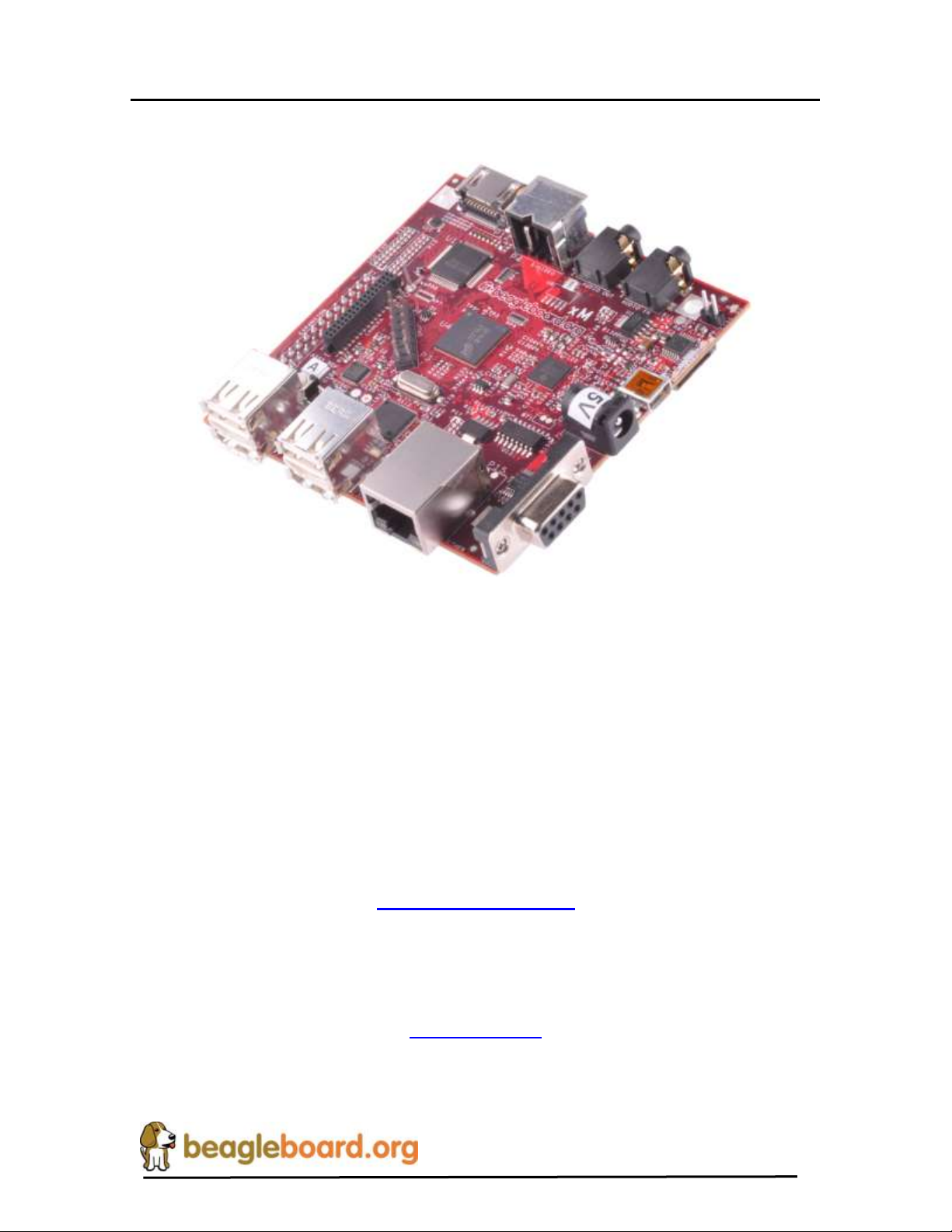
BeagleBoard-xM System
Reference Manual
Revision C2
BeagleBoard-xM Rev C2
System Reference Manual
Revision 0.0
October 11, 2012
Send all comments and errors concerning this SRM to the author at
For other questions you may contact Gerald at:
Gerald Coley
Texas Instruments
12500 TI Blvd. Dallas, Tx 75243
Page 1 of 163
Page 2

REF: BB_SRM_xM
BeagleBoard-xM System
Reference Manual
Revision C2
NOTE: This equipment has been tested and found to comply with the limits for a Class B
digital device, pursuant to Part 15 of the FCC Rules. These limits are designed to provide
reasonable protection against harmful interference when the equipment is operated in a
commercial environment. This equipment generates, uses, and can radiate radio
frequency energy and, if not installed and used in accordance with the instruction manual,
may cause harmful interference to radio communications. Operation of this equipment in a
residential area is likely to cause harmful interference in which case the user will be
required to correct the interference at their own expense. All accessories used with this
board must meet FCC certification to maintain compliance of this equipment.
NOTE:. If this equipment does cause harmful interference to radio or television reception, which
can be determined by turning the equipment off and on, the user is encouraged to try to correct the
interference by one or more of the following measures:
—Reorient or relocate the receiving antenna.
—Increase the separation between the equipment and receiver.
—Connect the equipment into an outlet on a circuit different from that to which the receiver is
connected.
—Consult the dealer or an experienced radio/TV technician for help.
Changes or modifications not expressly approved by this manual for compliance could void the
user’s authority to operate the equipment.
THIS DOCUMENT
This work is licensed under the Creative Commons Attribution-Share Alike 3.0 Unported
License. To view a copy of this license, visit http://creativecommons.org/licenses/by-
sa/3.0/ or send a letter to Creative Commons, 171 Second Street, Suite 300, San
Francisco, California, 94105, USA.
All derivative works are to be attributed to Gerald Coley of BeagleBoard.org.
For more information, see http://creativecommons.org/license/results-
one?license_code=by-sa
For any questions, concerns, or issues submit them to [email protected]
BEAGLEBOARD DESIGN
Page 2 of 163
Page 3

REF: BB_SRM_xM
BeagleBoard-xM System
Reference Manual
Revision C2
These design materials referred to in this document are
*NOT SUPPORTED* and DO NOT constitute a
reference design. Only “community” support is allowed via
resources at BeagleBoard.org/discuss.
THERE IS NO WARRANTY FOR THE DESIGN
MATERIALS, TO THE EXTENT PERMITTED BY
APPLICABLE LAW. EXCEPT WHEN OTHERWISE
STATED IN WRITING THE COPYRIGHT HOLDERS
AND/OR OTHER PARTIES PROVIDE THE DESIGN
MATERIALS “AS IS” WITHOUT WARRANTY OF
ANY KIND, EITHER EXPRESSED OR IMPLIED,
INCLUDING, BUT NOT LIMITED TO, THE IMPLIED
WARRANTIES OF MERCHANTABILITY AND
FITNESS FOR A PARTICULAR PURPOSE. THE
ENTIRE RISK AS TO THE QUALITY AND
PERFORMANCE OF THE DESIGN MATERIALS IS
WITH YOU. SHOULD THE DESIGN MATERIALS
PROVE DEFECTIVE, YOU ASSUME THE COST OF
ALL NECESSARY SERVICING, REPAIR OR
CORRECTION.
We mean it; these design materials may be totally
unsuitable for any purposes.
Page 3 of 163
Page 4

REF: BB_SRM_xM
BeagleBoard-xM System
Reference Manual
Revision C2
BeagleBoard.org provides the enclosed product(s) under the following conditions:
This evaluation board/kit is intended for use for ENGINEERING DEVELOPMENT, DEMONSTRATION, OR
EVALUATION PURPOSES ONLY and is not considered by BeagleBoard.org to be a finished end-product
fit for general consumer use. Persons handling the product(s) must have electronics training and observe
good engineering practice standards. As such, the goods being provided are not intended to be complete in
terms of required design-, marketing-, and/or manufacturing-related protective considerations, including
product safety and environmental measures typically found in end products that incorporate such
semiconductor components or circuit boards. This evaluation board/kit does not fall within the scope of the
European Union directives regarding electromagnetic compatibility, restricted substances (RoHS), recycling
(WEEE), FCC, CE or UL, and therefore may not meet the technical requirements of these directives or other
related directives.
Should this evaluation board/kit not meet the specifications indicated in the User’s Guide, the board/kit may
be returned within 30 days from the date of delivery for a full refund. THE FOREGOING WARRANTY IS
THE EXCLUSIVE WARRANTY MADE BY SELLER TO BUYER AND IS IN LIEU OF ALL OTHER
WARRANTIES, EXPRESSED, IMPLIED, OR STATUTORY, INCLUDING ANY WARRANTY OF
MERCHANTABILITY OR FITNESS FOR ANY PARTICULAR PURPOSE.
The user assumes all responsibility and liability for proper and safe handling of the goods. Further, the user
indemnifies BeagleBoard.org from all claims arising from the handling or use of the goods. Due to the open
construction of the product, it is the user’s responsibility to take any and all appropriate precautions with
regard to electrostatic discharge.
EXCEPT TO THE EXTENT OF THE INDEMNITY SET FORTH ABOVE, NEITHER PARTY SHALL BE
LIABLE TO THE OTHER FOR ANY INDIRECT, SPECIAL, INCIDENTAL, OR CONSEQUENTIAL
DAMAGES.
BeagleBoard.org currently deals with a variety of customers for products, and therefore our arrangement
with the user is not exclusive. BeagleBoard.org assumes no liability for applications assistance,
customer product design, software performance, or infringement of patents or services described
herein.
Please read the User’s Guide and, specifically, the Warnings and Restrictions notice in the User’s Guide
prior to handling the product. This notice contains important safety information about temperatures and
voltages. For additional information on BeagleBoard.org environmental and/or safety programs, please
contact visit BeagleBoard.org.
No license is granted under any patent right or other intellectual property right of BeagleBoard.org covering
or relating to any machine, process, or combination in which such BeagleBoard.org products or services
might be or are used.
Mailing Address:
BeagleBoard.org
1380 Presidential Dr. #100
Richardson, TX 75081
U.S.A.
Page 4 of 163
Page 5

REF: BB_SRM_xM
BeagleBoard-xM System
Reference Manual
Revision C2
WARRANTY: The BeagleBoard is warranted against defects in materials and workmanship for a
period of 90 days from purchase. This warranty does not cover any problems occurring as a result
of improper use, modifications, exposure to water, excessive voltages, abuse, or accidents. All
boards will be returned via standard mail if an issue is found. If no issue is found or express return
is needed, the customer will pay all shipping costs.
Before returning the board, please visit BeagleBoard.org/support
Please refer to sections 12 and 13 of this document for the board checkout procedures and
troubleshooting guides.
To return a defective board, please request an RMA at http://beagleboard.org/support/rma
Page 5 of 163
Page 6

REF: BB_SRM_xM
BeagleBoard-xM System
Reference Manual
Revision C2
Table of Contents
FIGURES .....................................................................................................................................................10
TABLES .......................................................................................................................................................12
1.0 INTRODUCTION..............................................................................................................................14
2.0 CHANGE HISTORY .........................................................................................................................16
2.1 CHANGE HISTORY ............................................................................................................................16
2.2 BEAGLEBOARD VS. BEAGLEBOARD-XM .........................................................................................16
2.2.1 Hardware Changes ................................................................................................................16
2.2.2 Software Changes ..................................................................................................................17
2.3 –XM REVISION A2 VS. –XM REVISION A3 .......................................................................................17
2.4 –XM REVISION A3 VS. –XM REVISION B .........................................................................................17
2.5 –XM REVISION B VS. –XM REVISION C ...........................................................................................18
2.6 –XM REVISION C VS. –XM REVISION C1 .........................................................................................19
2.7 DEFINITIONS ....................................................................................................................................19
3.0 BEAGLEBOARD OVERVIEW .......................................................................................................20
3.1 BEAGLEBOARD VERSIONS ...............................................................................................................20
4.0 BEAGLEBOARD SPECIFICATION ..............................................................................................21
4.1 BEAGLEBOARD FEATURES...............................................................................................................21
4.2 PROCESSOR ......................................................................................................................................22
4.3 MEMORY..........................................................................................................................................22
4.4 POWER MANAGEMENT.....................................................................................................................22
4.5 HS USB 2.0 OTG PORT ...................................................................................................................23
4.6 HS USB 2.0 HOST PORTS ................................................................................................................23
4.7 STEREO AUDIO OUTPUT CONNECTOR ..............................................................................................24
4.8 STEREO AUDIO IN CONNECTOR .......................................................................................................24
4.9 S-VIDEO CONNECTOR ......................................................................................................................24
4.10 DVI-D CONNECTOR ....................................................................................................................24
4.11 LCD HEADER ..............................................................................................................................24
4.12 MICROSD CONNECTOR ................................................................................................................25
4.13 RESET BUTTON ...........................................................................................................................25
4.14 USER BUTTON .............................................................................................................................25
4.15 INDICATORS ................................................................................................................................25
4.16 POWER CONNECTOR ...................................................................................................................25
4.17 JTAG CONNECTOR .....................................................................................................................26
4.18 RS232 DB9 CONNECTOR ............................................................................................................26
4.19 MAIN EXPANSION HEADER .........................................................................................................26
4.20 CAMERA CONNECTOR .................................................................................................................26
4.21 MMC3 EXPANSION HEADER .......................................................................................................27
4.22 MCBSP EXPANSION HEADER......................................................................................................27
4.23 BEAGLEBOARD MECHANICAL SPECIFICATIONS ..........................................................................27
4.24 ELECTRICAL SPECIFICATIONS .....................................................................................................28
5.0 PRODUCT CONTENTS ...................................................................................................................30
5.1 BEAGLEBOARD IN THE BOX ............................................................................................................30
5.2 SOFTWARE ON THE BEAGLEBOARD .................................................................................................31
5.3 REPAIRS ...........................................................................................................................................31
6.0 BEAGLEBOARD CONNECTIONS ................................................................................................32
Page 6 of 163
Page 7

REF: BB_SRM_xM
BeagleBoard-xM System
Reference Manual
Revision C2
6.1 CONNECTING USB OTG ..................................................................................................................32
6.2 CONNECTING USB HOST .................................................................................................................34
6.3 CONNECTING DC POWER .................................................................................................................35
6.4 CONNECTING JTAG .........................................................................................................................36
6.5 CONNECTING SERIAL CABLE ...........................................................................................................37
6.6 CONNECTING S-VIDEO .....................................................................................................................38
6.7 CONNECTING DVI-D CABLE ............................................................................................................39
6.8 CONNECTING STEREO OUT CABLE...................................................................................................40
6.9 CONNECTING STEREO IN CABLE ......................................................................................................41
6.10 INDICATOR LOCATIONS ...............................................................................................................42
6.11 BUTTON LOCATIONS ...................................................................................................................43
6.12 MICROSD CONNECTION ..............................................................................................................44
6.13 LCD CONNECTION ......................................................................................................................45
7.0 BEAGLEBOARD-XM SYSTEM ARCHITECTURE AND DESIGN ..........................................46
7.1 SYSTEM BLOCK DIAGRAM ...............................................................................................................46
7.2 OVER VOLTAGE PROTECTION ..........................................................................................................48
7.3 POWER CONDITIONING ....................................................................................................................49
7.3.1 USB DC Source .....................................................................................................................50
7.3.2 Wall Supply Source ................................................................................................................51
7.3.3 DC Source Control ................................................................................................................51
7.3.4 AUX 3.3V Supply ...................................................................................................................52
7.4 METER CURRENT MEASUREMENT ...................................................................................................53
7.5 PROCESSOR CURRENT MEASUREMENT ............................................................................................53
7.6 VBAT POWER CONDITIONING .........................................................................................................55
7.7 TPS65950 RESET AND POWER MANAGEMENT ................................................................................55
7.7.1 Main Core Voltages ...............................................................................................................56
7.7.2 Main DC Input .......................................................................................................................56
7.7.3 Processor I2C Control ...........................................................................................................56
7.7.4 VIO_1V8 ................................................................................................................................56
7.7.5 Main Core Voltages Smart Reflex .........................................................................................58
7.7.6 VDD1 .....................................................................................................................................58
7.7.7 VDD2 .....................................................................................................................................58
7.8 PERIPHERAL VOLTAGES ...................................................................................................................59
7.8.1 VDD_PLL2 ............................................................................................................................59
7.8.2 VDD_PLL1 ............................................................................................................................60
7.8.3 VDAC_1V8 ............................................................................................................................60
7.8.4 VDD_SIM ..............................................................................................................................61
7.8.5 VMMC2 .................................................................................................................................61
7.8.6 VDD_VMMC1 .......................................................................................................................61
7.8.7 CAM_2V8 ..............................................................................................................................61
7.8.8 CAM_1V8 ..............................................................................................................................61
7.8.9 USB_1V8 ...............................................................................................................................61
7.8.10 EXP_VDD .........................................................................................................................62
7.9 OTHER SIGNALS ...............................................................................................................................62
7.9.1 Boot Configuration ................................................................................................................62
7.9.2 RTC Backup Battery ..............................................................................................................62
7.9.3 Power Sequencing .................................................................................................................63
7.9.4 Reset Signals ..........................................................................................................................63
7.9.5 mSecure Signal ......................................................................................................................65
7.10 PROCESSOR .................................................................................................................................65
7.10.1 Overview ...........................................................................................................................66
7.10.2 SDRAM Bus ......................................................................................................................66
7.10.3 GPMC Bus ........................................................................................................................67
7.10.4 DSS Bus ............................................................................................................................67
Page 7 of 163
Page 8

REF: BB_SRM_xM
BeagleBoard-xM System
Reference Manual
Revision C2
7.10.5 McBSP2 ............................................................................................................................67
7.10.6 McBSP1 ............................................................................................................................67
7.10.7 McBSP3 ............................................................................................................................68
7.10.8 Pin Muxing ........................................................................................................................68
7.10.9 GPIO Mapping .................................................................................................................70
7.10.10 Interrupt Mapping .............................................................................................................70
7.11 POP MEMORY DEVICE ................................................................................................................71
7.12 SYSTEM CLOCKS .........................................................................................................................71
7.12.1 32KHz Clock .....................................................................................................................72
7.12.2 26MHz Clock ....................................................................................................................72
7.12.3 McBSP_CLKS ...................................................................................................................73
7.13 USB OTG PORT ..........................................................................................................................73
7.13.1 USB OTG Overview ..........................................................................................................73
7.13.2 USB OTG Design ..............................................................................................................74
7.13.3 OTG ULPI Interface .........................................................................................................74
7.13.4 OTG Charge Pump ...........................................................................................................75
7.13.5 OTG USB Connector ........................................................................................................76
7.13.6 OTG USB Protection ........................................................................................................76
7.14 ONBOARD USB HUB ..................................................................................................................76
7.14.1 Power ................................................................................................................................77
7.14.2 HS USB PHY .....................................................................................................................78
7.14.3 USB HUB ..........................................................................................................................80
7.14.4 USB Port Connectors ........................................................................................................82
7.14.5 Ethernet .............................................................................................................................83
7.15 MICROSD ....................................................................................................................................84
7.15.1 microSD Power .................................................................................................................84
7.15.2 Processor Interface ...........................................................................................................84
7.15.3 Card Detect .......................................................................................................................85
7.15.4 Booting From SD/MMC Cards .........................................................................................85
7.16 AUDIO INTERFACE ......................................................................................................................86
7.16.1 Processor Audio Interface ................................................................................................86
7.16.2 TPS65950 Audio Interface ................................................................................................87
7.16.3 Audio Output Jack ............................................................................................................87
7.16.4 Audio Input Jack ...............................................................................................................87
7.17 DVI-D INTERFACE ......................................................................................................................88
7.17.1 Processor LCD Interface ..................................................................................................89
7.17.2 LCD Power .......................................................................................................................90
7.17.3 TFP410 Power ..................................................................................................................90
7.17.4 TFP410 Framer ................................................................................................................90
7.17.5 TFP410 Control Pins ........................................................................................................91
7.17.6 DVI-D Connector ..............................................................................................................92
7.18 LCD EXPANSION HEADERS.........................................................................................................94
7.19 S-VIDEO ......................................................................................................................................96
7.20 CAMERA PORT ............................................................................................................................96
7.20.1 Camera Power ..................................................................................................................97
7.20.2 Camera I2C Port ..............................................................................................................98
7.20.3 Processor Camera Port Interface .....................................................................................98
7.20.4 Camera Modules .............................................................................................................100
7.21 RS232 PORT ..............................................................................................................................101
7.21.1 Processor Interface .........................................................................................................101
7.21.2 Level Translator ..............................................................................................................101
7.21.3 RS232 Transceiver ..........................................................................................................102
7.21.4 Connector .......................................................................................................................102
7.22 INDICATORS ..............................................................................................................................102
7.22.1 Power Indicator ..............................................................................................................103
Page 8 of 163
Page 9

REF: BB_SRM_xM
BeagleBoard-xM System
Reference Manual
Revision C2
7.22.2 PMU Status Indicator .....................................................................................................103
7.22.3 User Indicators ...............................................................................................................104
7.22.4 HUB Power Indicator .....................................................................................................104
7.22.5 Overvoltage Indicators ...................................................................................................104
7.23 JTAG ........................................................................................................................................104
7.23.1 Processor Interface .........................................................................................................105
7.23.2 JTAG Connector .............................................................................................................105
7.24 MAIN EXPANSION HEADER .......................................................................................................105
7.24.1 Processor Interface .........................................................................................................106
7.24.2 Expansion Signals ...........................................................................................................107
7.24.3 Power ..............................................................................................................................109
7.24.4 Reset ................................................................................................................................109
7.24.5 Power Control.................................................................................................................109
7.25 LCD EXPANSION HEADER ........................................................................................................109
7.26 AUXILIARY EXPANSION HEADER ..............................................................................................110
7.26.1 MCBSP5 Signals .............................................................................................................111
7.26.2 MMC3 Signals ................................................................................................................111
7.26.3 ETK Signals ....................................................................................................................112
7.26.4 HSUSB1 Signals .............................................................................................................113
7.26.5 Alternate Clock ...............................................................................................................113
7.26.6 HDQ 1-Wire ....................................................................................................................113
7.26.7 ADC ................................................................................................................................113
7.26.8 GPIO Signals ..................................................................................................................114
7.26.9 DMAREQ ........................................................................................................................114
7.27 AUDIO EXPANSION HEADER .....................................................................................................114
8.0 CONNECTOR PINOUTS AND CABLES ....................................................................................115
8.1 POWER CONNECTOR ......................................................................................................................115
8.2 USB OTG ......................................................................................................................................116
8.3 S-VIDEO.........................................................................................................................................117
8.4 DVI-D ...........................................................................................................................................118
8.5 LCD ...............................................................................................................................................120
8.5.1 Connector Pinout .................................................................................................................120
8.5.2 Camera ................................................................................................................................122
8.5.3 Audio McBSP2 Port .............................................................................................................124
8.5.4 Auxiliary Access Header ......................................................................................................125
8.5.5 LCD and Expansion Measurements ....................................................................................126
8.5.6 Mounting Scenarios .............................................................................................................127
8.6 AUDIO CONNECTIONS ....................................................................................................................128
8.7 AUDIO OUT ....................................................................................................................................129
8.8 JTAG .............................................................................................................................................130
8.9 BATTERY INSTALLATION ...............................................................................................................132
8.9.1 Battery .................................................................................................................................132
8.9.2 Battery Installation ..............................................................................................................132
9.0 BEAGLEBOARD ACCESSORIES ...............................................................................................134
9.1 DC POWER SUPPLY ........................................................................................................................135
9.2 DVI CABLES ..................................................................................................................................136
9.3 DVI-D MONITORS .........................................................................................................................136
9.4 MICROSD CARDS ...........................................................................................................................137
9.5 USB TO WIFI .................................................................................................................................137
9.6 USB TO BLUETOOTH .....................................................................................................................138
10.0 MECHANICAL INFORMATION ............................................................................................140
10.1 BEAGLEBOARD DIMENSIONS ....................................................................................................140
Page 9 of 163
Page 10

REF: BB_SRM_xM
BeagleBoard-xM System
Reference Manual
Revision C2
10.2 BEAGLEBOARD EXPANSION CARD DESIGN INFORMATION .......................................................141
10.2.1 Mounting Method ............................................................................................................141
10.2.2 Expansion EEPROM .......................................................................................................142
11.0 BOARD VERIFICATION TEST POINTS...............................................................................144
11.1.1 Signal Access Points .......................................................................................................146
11.2 TROUBLESHOOTING GUIDE .......................................................................................................147
12.0 KNOWN ISSUES ........................................................................................................................148
13.0 PCB COMPONENT LOCATIONS ...........................................................................................149
14.0 SCHEMATICS ............................................................................................................................151
15.0 BILLS OF MATERIAL..............................................................................................................162
16.0 PCB INFORMATION ................................................................................................................163
Figures
Figure 1. BeagleBoard and BeagleBoard-xM .............................................................. 20
Figure 2. USB Y-Cable ................................................................................................ 23
Figure 3. The -xM Rev C Box ...................................................................................... 30
Figure 4. -xM Rev C Box Contents .............................................................................. 31
Figure 5. USB OTG Connection .................................................................................. 33
Figure 6. USB Host Connection ................................................................................... 34
Figure 7. DC Power Connection .................................................................................. 35
Figure 8. BeagleBoard JTAG Connection ................................................................... 36
Figure 9. BeagleBoard Serial Cable Connection .......................................................... 37
Figure 10. BeagleBoard S-Video Connection ............................................................ 38
Figure 11. BeagleBoard DVI-D Connection .............................................................. 39
Figure 12. BeagleBoard Audio Out Cable Connection .............................................. 40
Figure 13. BeagleBoard Audio In Cable Connection................................................. 41
Figure 14. BeagleBoard Indicator Locations ............................................................. 42
Figure 15. BeagleBoard Button Location................................................................... 43
Figure 16. BeagleBoard microSD Card Location ...................................................... 44
Figure 17. BeagleBoard LCD Header Location ......................................................... 45
Figure 18. BeagleBoard-xM High Level Block Diagram .......................................... 46
Figure 19. BeagleBoard Major Components .............................................................. 47
Figure 20. Overvoltage Protection ............................................................................. 48
Figure 21. Input Power Section .................................................................................. 50
Figure 22. AUX 3.3 Power Section ............................................................................ 52
Figure 23. Processor Current Measurement ............................................................... 53
Figure 24. VBAT Power Conditioning ...................................................................... 55
Figure 25. Main Power Rails ...................................................................................... 57
Figure 26. Peripheral Voltages ................................................................................... 60
Figure 27. Power Sequencing ..................................................................................... 63
Figure 28. Reset Circuitry .......................................................................................... 64
Figure 29. DM37x Block Diagram............................................................................. 65
Page 10 of 163
Page 11

REF: BB_SRM_xM
BeagleBoard-xM System
Reference Manual
Revision C2
Figure 30. McBSP2 Interface ..................................................................................... 67
Figure 31. McBSP1 Interface ..................................................................................... 68
Figure 32. McBSP3 Interface ..................................................................................... 68
Figure 33. POP Memory ............................................................................................ 71
Figure 34. System Clocks ........................................................................................... 72
Figure 35. USB OTG Design ..................................................................................... 74
Figure 36. USB HUB Block Diagram ........................................................................ 77
Figure 37. HUB Power Circuitry ............................................................................... 78
Figure 38. USB PHY Design ..................................................................................... 79
Figure 39. USB HUB Design ..................................................................................... 81
Figure 40. USB Port Power Design............................................................................ 82
Figure 41. USB Based Ethernet Design ..................................................................... 83
Figure 42. microSD Interface ..................................................................................... 84
Figure 43. Audio Circuitry ......................................................................................... 86
Figure 44. DVI-D Interface ........................................................................................ 88
Figure 45. S-Video Interface ...................................................................................... 96
Figure 46. Camera Port Interface ............................................................................... 97
Figure 47. Camera Modules ..................................................................................... 101
Figure 48. RS232 Interface Design .......................................................................... 101
Figure 49. Indicator Design ...................................................................................... 103
Figure 50. JTAG Interface........................................................................................ 105
Figure 51. Main Expansion Header Processor Connections .................................... 106
Figure 52. Power Connector ..................................................................................... 115
Figure 53. USB OTG Connector .............................................................................. 116
Figure 54. OTG Host Shorting Pads ........................................................................ 116
Figure 55. S-Video Connector.................................................................................. 117
Figure 56. DVI-D Connector.................................................................................... 118
Figure 57. DVI-D Cable ........................................................................................... 119
Figure 58. DVI-D Cable ........................................................................................... 119
Figure 59. LCD Expansion Connector Pins ............................................................. 121
Figure 60. Camera Connector .................................................................................. 123
Figure 61. Camera Module ....................................................................................... 123
Figure 62. McBSP Audio Connector ....................................................................... 124
Figure 63. Auxiliary Access Connector ................................................................... 125
Figure 64. Top Mount LCD Adapter........................................................................ 126
Figure 65. Bottom Mount LCD Adapter .................................................................. 127
Figure 66. Audio In Plug .......................................................................................... 128
Figure 67. Audio In Connector................................................................................. 128
Figure 68. Audio Out Plug ....................................................................................... 129
Figure 69. Audio Out Connector .............................................................................. 129
Figure 70. JTAG Connector Pinout .......................................................................... 130
Figure 71. JTAG 14 to 20 Pin Adapter .................................................................... 131
Figure 72. JTAG Cable Placement ........................................................................... 131
Figure 73. Optional Battery ...................................................................................... 132
Figure 74. Optional Battery Location....................................................................... 133
Figure 75. Resistor R65 ............................................................................................ 133
Page 11 of 163
Page 12

REF: BB_SRM_xM
BeagleBoard-xM System
Reference Manual
Revision C2
Figure 76. DC Power Supply ................................................................................... 135
Figure 77. HDMI to DVI-D Cable .......................................................................... 136
Figure 78. USB to WiFi ........................................................................................... 137
Figure 79. USB to Bluetooth .................................................................................... 138
Figure 80. BeagleBoard Dimension Drawing .......................................................... 140
Figure 81. BeagleBoard Bottom Stacked Daughter Card ....................................... 141
Figure 82. BeagleBoard-xM Expansion Headers ..................................................... 142
Figure 83. BeagleBoard Expansion Board EEPROM Schematic ............................ 143
Figure 84. BeagleBoard Voltage Access Points ....................................................... 144
Figure 85. BeagleBoard Signal Access Points ......................................................... 146
Figure 86. BeagleBoard Top Side Components ....................................................... 149
Figure 87. BeagleBoard Bottom Side Components ................................................. 150
Tables
Table 1. Change History ............................................................................................. 16
Table 2. BeagleBoard-xM Features ............................................................................ 21
Table 3. BeagleBoard Electrical Specification -xM Rev C ........................................ 28
Table 4. Processor Pin Muxing Settings ..................................................................... 69
Table 5. Processor GPIO Pins ..................................................................................... 70
Table 6. Processor Interrupt Pins ................................................................................ 70
Table 7. Processor ULPI Interface .............................................................................. 75
Table 8. TPS65950 ULPI Interface ............................................................................. 75
Table 9. USB OTG Charge Pump Pins ....................................................................... 76
Table 10. USB Host Port OMAP Signals ..................................................................... 79
Table 11. SD/MMC OMAP Signals ............................................................................. 84
Table 12. Processor Audio Signals ............................................................................... 86
Table 13. Processor Audio Signals ............................................................................... 87
Table 14. Processor LCD Signals ................................................................................. 89
Table 15. TFP410 Interface Signals .............................................................................. 90
Table 16. P11 LCD Signals........................................................................................... 94
Table 17. P13 LCD Signals........................................................................................... 95
Table 18. S-Video Interface Signals ............................................................................. 96
Table 19. Camera Interface Signals .............................................................................. 98
Table 20. Camera Pin Signal Mapping ......................................................................... 99
Table 21. JTAG Signals .............................................................................................. 105
Table 22. Expansion Connector Signals ..................................................................... 107
Table 23. Expansion Connector Signal Groups .......................................................... 108
Table 24. P11 GPIO Signals ....................................................................................... 110
Table 25. P13 GPIO Signals ....................................................................................... 110
Table 26. P17 Auxiliary Expansion Signals ............................................................... 111
Table 27. P17 McBSP5 Expansion Signals ................................................................ 111
Table 28. P17 MMC3 Expansion Signals ................................................................... 112
Table 29. P17 Auxiliary ETK Signals ........................................................................ 112
Table 30. P17 High Speed USB Expansion Signals ................................................... 113
Table 31. P17 Auxiliary GPIO Signals ....................................................................... 114
Page 12 of 163
Page 13

REF: BB_SRM_xM
BeagleBoard-xM System
Reference Manual
Revision C2
Table 32. DVI-D to HDMI Cable ............................................................................... 118
Table 33. P11 LCD Signals......................................................................................... 120
Table 34. P13 LCD Signals......................................................................................... 121
Table 35. P10 Camera Signals .................................................................................... 122
Table 36. P10 McBSP2 Signals .................................................................................. 124
Table 37. P17 Auxiliary Access Signals ..................................................................... 125
Table 38. Connector Dimensions ................................................................................ 126
Table 39. JTAG Signals .............................................................................................. 130
Table 40. DC Power Supply Specifications ................................................................ 135
Table 41. DC Power Supplies ..................................................................................... 135
Table 42. DVI-D Monitors Tested .............................................................................. 136
Table 43. SD/MMC Cards Tested............................................................................... 137
Table 44. USB to WiFi Adapters ................................................................................ 138
Table 45. USB to Bluetooth Adapters ........................................................................ 139
Table 46. Voltages ...................................................................................................... 145
Table 47. Troubleshooting .......................................................................................... 147
Table 48. Known Issues .............................................................................................. 148
NOTES
Page 13 of 163
Page 14

REF: BB_SRM_xM
BeagleBoard-xM System
Reference Manual
Revision C2
1.0 Introduction
This document is the System Reference Manual for the BeagleBoard-xM, a low cost
ARM Cortex A8 board supported through BeagleBoard.org. This document provides
detailed information on the overall design and usage of the BeagleBoard from the system
level perspective. It is not intended to provide detailed documentation of the processor or
any other component used on the board. It is expected that the user will refer to the
appropriate documents for these devices to access detailed information.
The processor used on the BeagleBoard-xM is compatible with several Cortex A8
processors manufactured by Texas Instruments. Currently, the processor is a DM3730
processor manufactured and sold by Texas Instruments and information on this can be
found at the TI website. Additional information for the ARM only version, AM3715, can
also be found on the TI website. The key difference between the AM3715 and the
DM3730, is that the DSP is not included on the AM3715.
For the remainder of this document the DM3730 will be referred to as the processor.
The key sections in this document are:
Section 2.0– Change History
Provides tracking for the changes made to the System Reference Manual.
Section 3.0– Definitions and References
This section provides definitions for commonly used terms and acronyms.
Section 4.0– Overview
This is a high level overview of the BeagleBoard.
Section 5.0– Specification
Provided here are the features and electrical specifications of the BeagleBoard.
Section 6.0-Product Contents
Describes what the BeagleBoard package looks like and what is included in the
box.
Section 7.0– Connections
Covered here is how to connect the various cables to the BeagleBoard.
Section 8.0– System Architecture and Design
This section provides information on the overall architecture and design of the
BeagleBoard. This is a very detailed section that goes into the design of each
circuit on the board.
Section 9.0– Connector Pinouts and Cables
The section describes each connector and cable used in the system. This will
allow the user to create cables, purchase cables, or to perform debugging as
needed.
Page 14 of 163
Page 15

REF: BB_SRM_xM
BeagleBoard-xM System
Reference Manual
Revision C2
Section 10.0– BeagleBoard Accessories
Covered in this section are a few of the accessories that may be used with
BeagleBoard. This is not an exhaustive list, but does provide an idea of the types
of cables and accessories that can be supported and how to find them. It also
provides a definition of what they need to be. It does not guarantee that these
devices will work on all OS implementations.
Section 11.0 – Mechanical
Information is provided here on the dimensions of the BeagleBoard.
Section 12.0 – Troubleshooting
Here is where you can find tips on troubleshooting the setup of the BeagleBoard.
Section 13.0- Known Issues
This section describes the known issues with the current revision of the
BeagleBoard and any workarounds that may be possible.
Section 14.0- BeagleBoard Components
This section provides information on the top and bottom side silkscreen of the
BeagleBoard showing the location of the components.
Section 15.0- BeagleBoard Schematics
These are the schematics for the BeagleBoard and information on where to get the
PDF and OrCAD files..
Section 16.0- Bill Of Material
This section describes where to get the latest Bill of Material for the BeagleBoard.
Section 17.0- BeagleBoard PCB Information
This section describes where to get the PCB file information for the BeagleBoard.
Page 15 of 163
Page 16
REF: BB_SRM_xM
BeagleBoard-xM System
Reference Manual
Revision C2
Rev
Changes
Date
By
A
Initial release.
6/4/2010
GC
A1
Updated to new power OVP scheme
6/21/2020
GC
A2
Updated with camera and Memory information
7/23/2010
GC
A3
Moved to Rev B PCB.
10/18/2010
GC
B
Moved to ES1.1 silicon revision.
10/26/2010
GC
C
Design changes and moved to revision ES1.2 silicon
4/4/2010
GC
C1.1
Changed Table 5 to reflect GPIO4 instead of GPIO7for the user button.
Change section 7.20.1.1 to reflect I2C1 instead of I2C2.
1/17/201
GC
C2
Changed POP memory part number due to obsolescence of the current device.
10/11/2012
GC
AREA
BeagleBoard-xM
BeagleBoard
Comments
Processor
DM3730
OMAP3530
ARM Frequency
1GHZ
720MHz
DSP Frequency
800Mhz
520MHz
SGX Frequency
200Mhz
110MHz
DDR
512MB
256MB
DDR Speed
166MHz
166MHz
NAND 0 256MB
SD Connector
uSD
MMC/SD
USB Host Ports
4
1
Host Port Speed
FS/LS/HS
HS
Serial Connector
DB9
Header
Direct connect to USB to
Serial Cable
Camera Header
Yes
No
Leopard Imaging Camera
module
Ships with 4G SD
Yes
No
Contains bootable desktop
Overvoltage Protection
Yes
No
Power LED turnoff
Yes
No
Serial Port Power
Turnoff
Yes
No
2.0 Change History
2.1 Change History
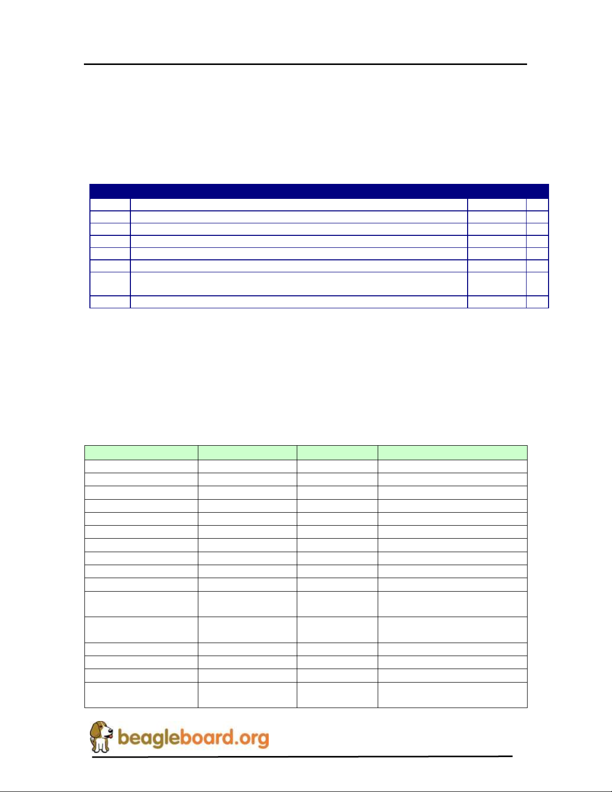
Table 1 tracks the changes made for each revision of this document.
Table 1. Change History
2.2 BeagleBoard vs. BeagleBoard-xM
There are several differences between the BeagleBoard and the BeagleBoard-xM . The
BeagleBoard refers to the original board and the BeagleBoard-xM is the newer version.
2.2.1 Hardware Changes
Page 16 of 163
Page 17

REF: BB_SRM_xM
BeagleBoard-xM System
Reference Manual
Revision C2
MMC3 Expansion
Header
Yes
No
McBSP2 Expansion
Header
Yes
No
2.2.2 Software Changes
Following are the changes to the SW.
o Use of a universal Beagle XLoader and UBoot. These will work on any Beagle
made. They include support for the 512MB DDR and the removal of the NAND
from the –xM board.
o A demo version of the Angstrom desktop distribution.
2.3 –xM Revision A2 vs. –xM Revision A3
There were no major hardware feature changes between the Rev A2 and Rev A3
revisions. Below are the differences between the Rev A2 and Rev A3 revisions.
o Slightly modified PCB layout (Rev B) to correct the following
o Changed silkscreen on L12 to R159 to reflect the usage of a resistor
instead of an inductor. Resistor was used on Rev A2. No electrical
difference.
o Changed routing on R66 and R68 to make them separate paths instead of
parallel. No electrical difference.
o Added 33 ohm resistor R157 in series with MMC clock line. Not used on
board, only for expansion. No electrical difference.
o Added R158 to allow isolation of drain pin on TPS2141. Loaded with a
zero ohm resistor. No electrical difference.
o Moved DVI_PUP pin to the TPS65950 GPIO2. No SW impact and
Angstrom kernel, however, updated SW can be used to turn off the DVI
interface by taking the pin LO. There may be issues with other
distributions until such time as their code is updated. Electrical change
from A2.
o Added R160 and R155 as a possible future option. Not populated on Rev
A3. No electrical difference.
o Changed R120 to 0603 package to align with arts purchased. No electrical
difference.
o Added R156 to remove the required lifting of U18 pin 4. Resistor is not
loaded on Revision A3. No electrical difference.
2.4 –xM Revision A3 vs. –xM Revision B
The only change from Rev –A3 to the Rev B was the replacement of the processor form
ES1.0 to ES1.1. For a detailed description of the issues present in the ES1.1 revision,
Page 17 of 163
Page 18

REF: BB_SRM_xM
BeagleBoard-xM System
Reference Manual
Revision C2
please refer to http://focus.ti.com/lit/er/sprz319a/sprz319a.pdf . There are no issues
resolved by ES1.1 that are anticipated to have any impact on the operation of the
BeagleBoard-xM.
2.5 –xM Revision B vs. –xM Revision C
There were seven changes made to the BeagleBoard-xM Rev C version over the Rev B
design.
o Resistor loading was changed to allow for the reading of the Rev C
revision by the SW. GPIO171=0, GPIO_172=1, and GPIO_173=0.
o Replacement of the processor from ES1.1 to ES1.2. For a detailed
description of the issues present in the ES1.2 revision, please refer to
http://focus.ti.com/lit/er/sprz319a/sprz319a.pdf . There are no issues
resolved by ES1.2 that are anticipated to have any impact on the operation
of the BeagleBoard-xM. ES1.2 is the latest revision.
o Fixed capacitor footprint in the PCB layout.
o Replaced the microSD connector with a new part. The current part was
targeted for EOL and a new one was required. This required a PCB
footprint change.
o Redesigned the overvoltage protection circuit. We were seeing issues with
a small number of boards being damaged on the TPS2054 USB power
FET, so a new design was implemented. Overall operation is the same as
the original version with te exception that it is now possible to power the
entire board over the USB OTG port. This includes the HUB. Care should
be taken not to add high current devices on the USB ports as that will
cause the host to shut down the USB port,
o Changed the default power state of the USB HUB to OFF as an added
layer of protection to make sure the USB power rails are off on initial
power up. This will minimize the initial current drain on the board. SW
can turn on the HUB power as needed by setting the TPS65950
LEDA/VIBRA.P pin LO to turn it on.
o Added the ability for the SW to detect when the board is powered from the
DC supply or the OTG supply. Status is read from GPIO.6 pin on the
TPS65950. If LO, then the board is powered from the DC jack. The HUB
will only work in the DC powered mode so this change allows the board to
know not to try and initialize the USB Host when under OTG power.
Page 18 of 163
Page 19

REF: BB_SRM_xM
BeagleBoard-xM System
Reference Manual
Revision C2
2.6 –xM Revision C vs. –xM Revision C1
There was only one change made on the Revision C1 board. The pads on the expansion
headers wee beefed up to address some issues we were seeing where there was a
disconnect between the etch and the pads inside the PCBs.
2.7 –xM Revision C1 vs. –xM Revision C2
There was only one change made on the Revision C2 board. The LPDDR POP memory is
being made obsolete by Micron. The new part is being used on the manufacture of the
revision C1 board. There are no functional differences as a result of this change. And no
SW changes are required. The new part number is MT46H128M32L2KQ-5 WT:B.
2.8 Definitions
SD- Secure Digital
microSD- Small version of the standard SD card
MDDR- Mobile Dual Data Rate
SDRAM- Synchronous Dynamic Random Access Memory
BeagleBoard- The original version of the board based on the DM3530
BeagleBoard-xM- The newer version of the board based on the DM3730.
Page 19 of 163
Page 20
REF: BB_SRM_xM
BeagleBoard-xM System
Reference Manual
Revision C2
3.0 BeagleBoard Overview
The BeagleBoard is designed specifically to address the Open Source Community. It has
been equipped with a minimum set of features to allow the user to experience the power
of the processor and is not intended as a full development platform as many of the
features and interfaces supplied by the processor are not accessible from the
BeagleBoard. By utilizing standard interfaces, the BeagleBoard is highly extensible to
add many features and interfaces. It is not intended for use in end products. All of the
design information is freely available and can be used as the basis for a product.
BeagleBoards will not be sold for use in any product as this hampers the ability to get the
boards to as many community members as possible and to grow the community.
3.1 BeagleBoard Versions
There are two different versions of the beagle in production, the BeagleBoard and the
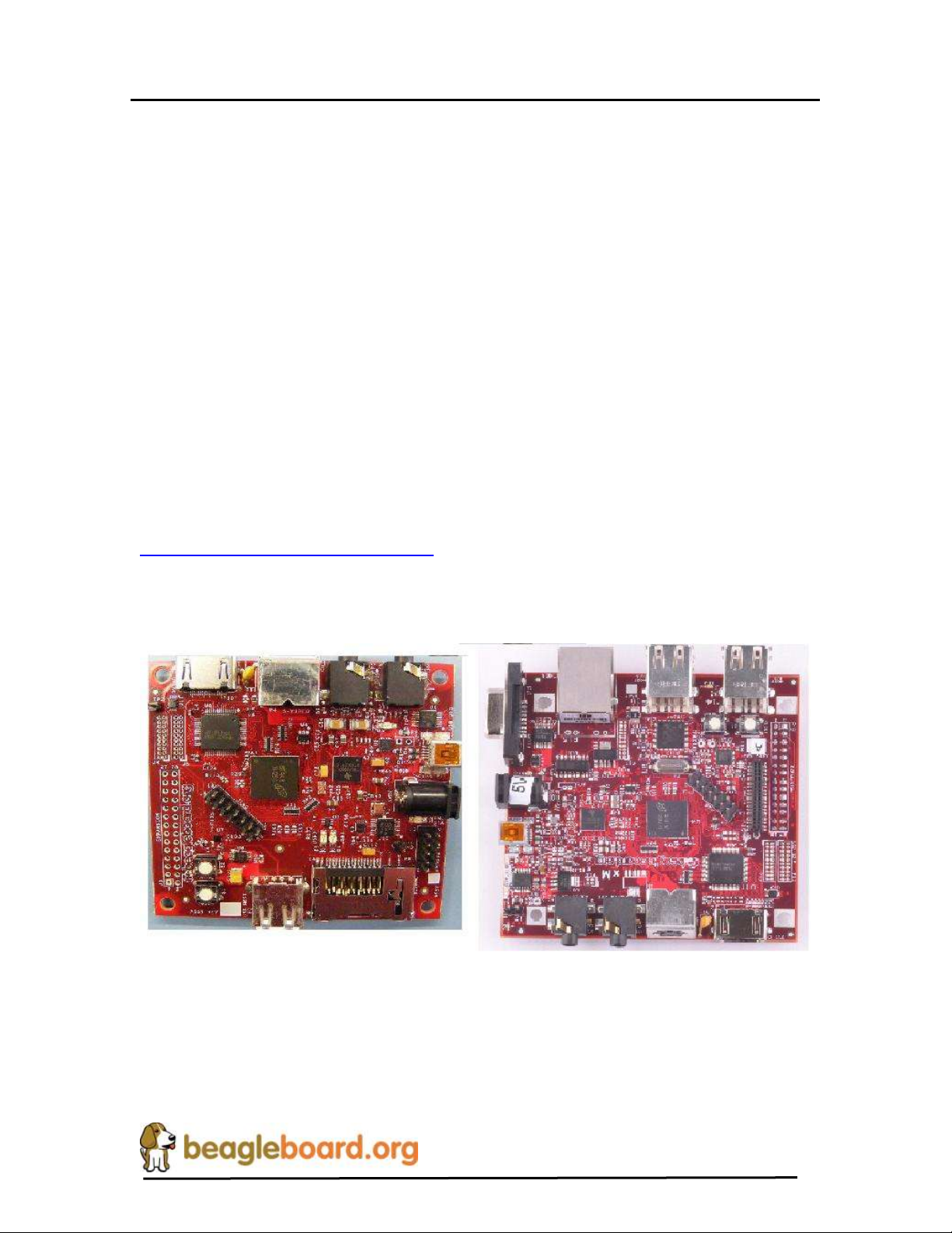
BeagleBoard–xM. Figure 1 is a picture of each of these versions. This manual covers the
revision A and B of the –xM version only. Please refer to the BeagleBoard System
Reference Manual for information on that version. It can be found at
http://beagleboard.org/hardware/design .
The Figure 1 shows pictures of the two different versions. The BeagleBoard is on the
left and the BeagleBoard–xM is on the right.
Figure 1. BeagleBoard and BeagleBoard-xM
Page 20 of 163
Page 21
REF: BB_SRM_xM
BeagleBoard-xM System
Reference Manual
Revision C2
Feature
Processor
Texas Instruments Cortex A8 1GHz processor
POP Memory
Micron 4Gb MDDR SDRAM (512MB) 200MHz
PMIC TPS65950
Power Regulators
Audio CODEC
Reset
USB OTG PHY
Debug Support
14-pin JTAG
GPIO Pins
UART
3 LEDs
PCB
3.1” x 3.0” (78.74 x 76.2mm)
6 layers
Indicators
Power, Power Error
2-User Controllable
PMU
USB Power
HS USB 2.0 OTG Port
Mini AB USB connector
TPS65950 I/F
USB Host Ports
SMSC LAN9514 Ethernet HUB
4 FS/LS/HS
Up to 500ma per Port if adequate
power is supplied
Ethernet
10/100
From USB HUB
Audio Connectors
3.5mm
3.5mm
L+R out
L+R Stereo In
SD/MMC Connector
MicroSD
User Interface
1-User defined button
Reset Button
Video
DVI-D
S-Video
Camera
Connector
Supports Leopard Imaging Module
Power Connector
USB Power
DC Power
Overvoltage Protection
Shutdown @ Over voltage
Main Expansion
Connector
Power (5V & 1.8V)
UART
McBSP
McSPI
I2C
GPIO
MMC2
PWM
2 LCD Connectors
Access to all of the LCD control
signals plus I2C
3.3V, 5V, 1.8V
Auxiliary Audio
4 pin connector
McBSP2
Auxiliary Expansion
MMC3
GPIO,ADC,HDQ
4.0 BeagleBoard Specification
This section covers the specifications of the BeagleBoard and provides a high level
description of the major components and interfaces that make up the BeagleBoard.
4.1 BeagleBoard Features
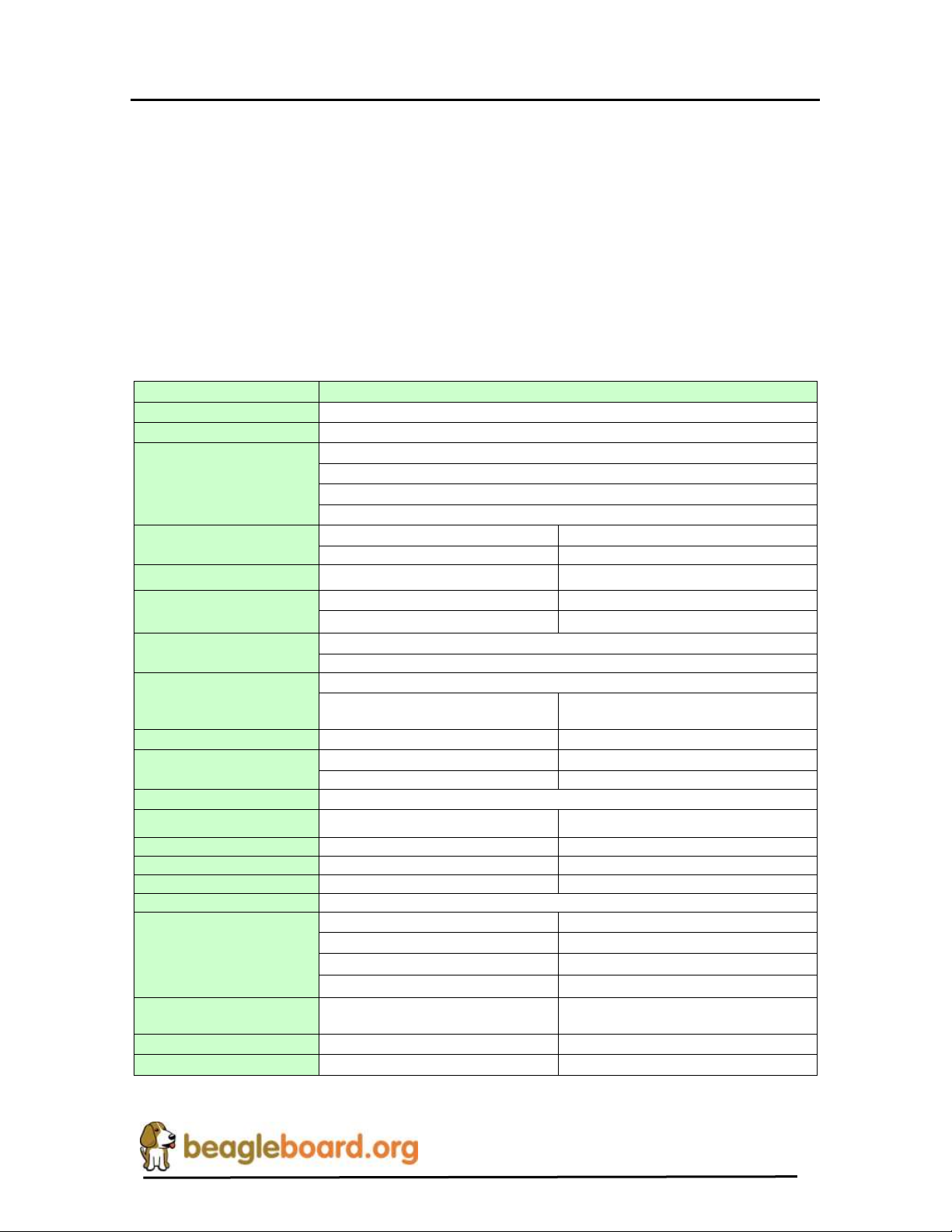
Table 2 provides a list of the BeagleBoard’s features.
Table 2. BeagleBoard-xM Features
Page 21 of 163
Page 22

REF: BB_SRM_xM
BeagleBoard-xM System
Reference Manual
Revision C2
The following sections provide more detail on each feature and sections of the
BeagleBoard.
4.2 Processor
The BeagleBoard-xM processor is the DM3730CBP 1GHz version and comes in a .4mm
pitch POP package. POP (Package on Package) is a technique where the memory is
mounted on top of the processor. For this reason, when looking at the BeagleBoard, you
will not find an actual part labeled DM3730CBP, but instead see the part number for the
memory.
4.3 Memory
There are two possible memory devices used on the –xM. The -00 assembly uses the
Micron POP memory and the -01 uses the Numonyx POP memory. The key function of
the POP memory is to provide:
o 4Gb MDDR SDRAM x32 (512MB @ 166MHz)
Unlike with earlier versions of the board, no other memory devices are on the
BeagleBoard. It is possible however, that additional non volatile memory storage can be
added to BeagleBoard by:
o Accessing the memory on the uSD card
o Use the USB OTG port and a powered USB hub to drive a USB Thumb drive or
hard drive.
o Install a thumbdrive into one of the USB ports
o Add a USB to Hard Disk adapter to one of the USB ports
Support for these devices is dependent upon driver support in the OS.
4.4 Power Management
The TPS65950 is used on the BeagleBoard to provide power with the exception of a 3.3V
regulator which is used to provide power to the DVI-D encoder and RS232 driver and an
additional 3.3V regulator to power the USB Hub. In addition to the power the TPS65950
also provides:
o Stereo Audio Out
o Stereo Audio in
o Power on reset
o USB OTG PHY
o Status LED
Page 22 of 163
Page 23
REF: BB_SRM_xM
BeagleBoard-xM System
Reference Manual
Revision C2
4.5 HS USB 2.0 OTG Port
The USB OTG port can be used as the primary power source and communication link for
the BeagleBoard and derives power from the PC over the USB cable. The client port is
limited in most cases to 500mA by the PC. There are instances where the PC or laptop
does not supply sufficient current to power the board as it does not provide the full
500mA. Under this mode the USB HUB will now be powered based on the design
changes made to the over volt circuitry. Care should be taken not to overload the USB
ports as the total power supplied to the ports will not enable full power to all of the USB
ports as you can have with the DC power.
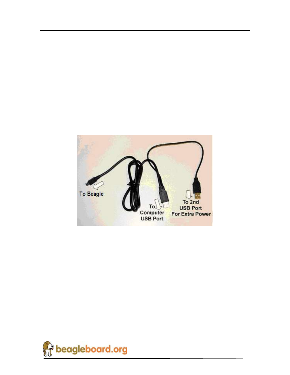
It is possible to take the current supplied by the USB ports to 1A by using a Y cable.
Figure 2 shows and example of the Y-Cable for the USB.
Figure 2. USB Y-Cable
The BeagleBoard requires a Y-Cable minAB to USB A cable or as mentioned a single
cable can be used if the USB Hub is powered down or not loaded on all of the ports.
4.6 HS USB 2.0 Host Ports
On the board are four USB Type A connectors with full LS/FS/HS support. Each port can
provide power on/off control and up to 500mA of current at 5V as long as the input DC is
at least 3A. The ports will not function unless the board is powered by the DC jack. They
cannot be powered via the OTG port.
Page 23 of 163
Page 24

REF: BB_SRM_xM
BeagleBoard-xM System
Reference Manual
Revision C2
4.7 Stereo Audio Output Connector
A 3.5mm standard stereo output audio jack is provided to access the stereo output of the
onboard audio CODEC. The audio CODEC is provided inside the TPS65950.
4.8 Stereo Audio In Connector
A 3.5mm standard stereo audio input jack is provided to access the stereo output of the
onboard audio CODEC.
4.9 S-Video Connector
A 4 pin DIN connector is provided to access the S-Video output of the BeagleBoard. This
is a separate output from the processor and can contain different video output data from
what is found on the DVI-D output if the software is configured to do it.
It will support NTSC or PAL format output to a standard TV. The default is NTSC, but
can be changed via the Software.
4.10 DVI-D Connector
The BeagleBoard can drive a LCD panel equipped with a DVI-D digital input. This is
the standard LCD panel interface of the processor and will support 24b color output.
DDC2B (Display Data Channel) or EDID (Enhanced Display ID) support over I2C is
provided in order to allow for the identification of the LCD monitor type and the required
settings.
The BeagleBoard is equipped with a DVI-D interface that uses an HDMI connector that
was selected for its small size. It does not support the full HDMI interface and is used to
provide the DVI-D interface portion only. The user must use a HDMI to DVI-D cable or
adapter to connect to a LCD monitor. This cable or adapter is not provided with the
BeagleBoard. A standard HDMI cable can be used when connecting to a monitor with an
HDMI connector.
DO NOT PLUG IN THE DVI-D CONNECTOR TO A DISPLAY WITH THE
BEAGLEBAORD POWERED ON. PLUG IN THE CABLE TO THE DISPLAY
AND THEN POWER ON THE BEAGLEBOARD.
4.11 LCD Header
A pair of 1.27mm pitch 2x10 headers are provided to gain access to the LCD signals.
This allows for the creation of LCD boards that will allow adapters to be made to provide
the level translation to support different LCD panels.
Page 24 of 163
Page 25

REF: BB_SRM_xM
BeagleBoard-xM System
Reference Manual
Revision C2
4.12 microSD Connector
A single microSD connector is provided as a means for the main non-volatile memory
storage on the board. This replaces the 6 in 2 SD/MMC connector found on the
BeagleBoard.
4.13 Reset Button
When pressed and released, causes a power on reset of the BeagleBoard.
4.14 User Button
A button is provided on the BeagleBoard to be used as an application button that can be
used by SW as needed. As there is no NAND boot option on the board, this button is no
longer needed to force an SD card boot. It is can be used by the UBoot SW to switch
between user scripts to allow different boot configurations to be selected as long as that
feature is included in the UBoot used. If you press this button on power up, the board will
not boot properly.
4.15 Indicators
There are five green LEDs on the BeagleBoard that can be controlled by the user.
o One on the TPS65950 that is programmed via the I2C interface
o Two on the processor controlled via GPIO pins
o One Power LED that indicates that power is applied and can be turned off
via SW.
o One to indicate that power is applied to the onboard USB HUB and can be
controlled via the SW.
There is also one red LED on the BeagleBoard that provides an indication that the power
connected to the board exceeds the voltage range of the board. If this LED ever turns on,
please remove the power connector and look for the correct power supply in order to
prevent damage to the board.
4.16 Power Connector
Power can be supplied via the USB OTG connector for some application that does not
require the USB Host ports. A wall supply 5V can be plugged into the DC power jack fro
full access to all functions of the board. When the wall supply is plugged in, it will
remove the power path from the USB connector and will be the power source for the
whole board. The power supply is not provided with the BeagleBoard.
Page 25 of 163
Page 26

REF: BB_SRM_xM
BeagleBoard-xM System
Reference Manual
Revision C2
When using the USB OTG port in the host mode, the DC supply must be connected as
the USB port will be used to provide limited power to the hub at a maximum of 100mA,
so the hub must be powered. The 100mA is not impacted by having a higher amperage
supply plugged into the DC power jack. The 100mA is a function of the OTG port itself.
Make sure the DC supply is regulated and a clean supply. If the power is over the voltage
specification, a RED LED will turn on. This will prevent the power from actually making
it to the circuitry on the board and will stay on as long as the power exceeds the voltage
specification.
4.17 JTAG Connector
A 14 pin JTAG header is provided on the BeagleBoard to facilitate the SW development
and debugging of the board by using various JTAG emulators. The interface is at 1.8V on
all signals. Only 1.8V Levels are supported. DO NOT expose the JTAG header to
3.3V.
4.18 RS232 DB9 Connector
Support for RS232 via UART3 is provided by DB9 connector on the BeagleBoard for
access to an onboard RS232 transceiver. A USB to Serial cable can be plugged directly
into the Beagle. Unlike on the original version of the Beagle, a straight through non null
modem cable is required. The cable you used on the BeagleBoard will NOT work on the
–xM version. A standard male to female straight DB9 cable may be used or you can use a
USB to serial adapter that will plug directly into the board without the need for any other
cables.
4.19 Main Expansion Header
A single 28 pin header is provided on the board to allow for the connection of various
expansion cards that could be developed by the users or other sources. Due to
multiplexing, different signals can be provided on each pin. This header is populated on
each board.
4.20 Camera Connector
A single connector has been added to the BeagleBoard–xM board for the purpose of
supporting a camera module. The camera module does not come with the board but can
be obtained from Leopard Imaging. The supported resolutions include VGA, 2MP, 3MP,
and 5MP camera modules. For proper operation of the cameras, the correct SW drivers
are required. This connector is populated on the board and is ready for the camera module
to be installed.
Page 26 of 163
Page 27

REF: BB_SRM_xM
BeagleBoard-xM System
Reference Manual
Revision C2
4.21 MMC3 Expansion Header
New to the BeagleBoard-xM is a 20 pin connector provided to allow access to additional
signals including GPIO and the MMC3 port. This connector is populated on the board.
4.22 McBSP Expansion Header
A 4 pin connector is provided to allow access to the McBSP2 signals for audio
applications. In order to use these signals, the audio interface on the TPS65950 must be
disabled by the SW. This connector is populated on the board..
4.23 BeagleBoard Mechanical Specifications
Size: 3.35” x 3.45”
Max height: TBM
Layers: 6
PCB thickness: .062”
RoHS Compliant: Yes
Weight: TBW
Page 27 of 163
Page 28
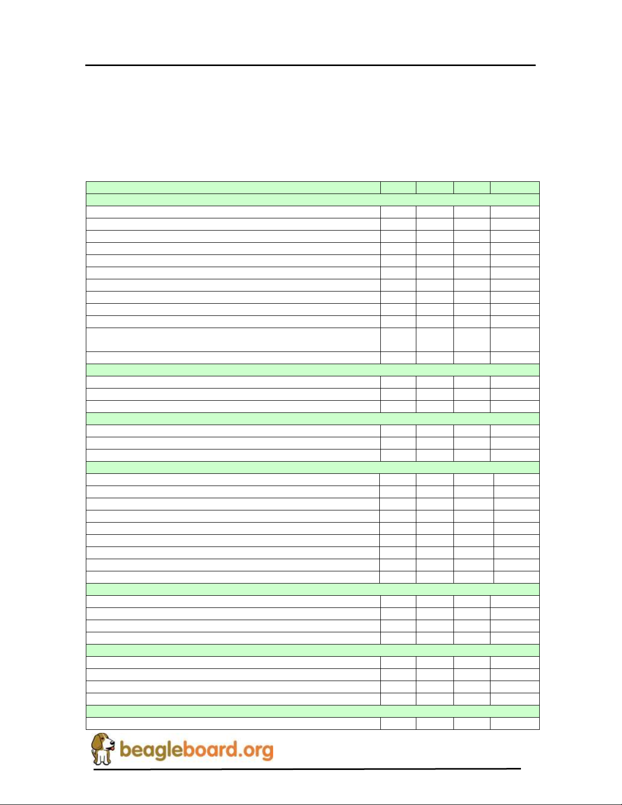
REF: BB_SRM_xM
BeagleBoard-xM System
Reference Manual
Revision C2
Specification
Min
Typ
Max
Unit
Power
Input Voltage USB
5 5.2 V Current USB
350 mA
Input Voltage DC
4.8 5 5.2 V Current DC
750 mA
Max Voltage without damage
12 V Expansion Voltage (5V)
4.8 5 5.2 V Curent (Dépends on source curent available)
750 A
Expansion Voltage (1.8V)
1.75
1.8
1.85
V
Current
30
mA
USB Host (Same as the DC supplied by the power plug or USB 5V)
4.8 5 5.2
V
Current (Depends on what the DC source can supply over
what the board requires)
Varies
Maximum current supplied by all four USB Host ports Total
1500 mA
USB OTG
High Speed Mode
480
Mb/S
Full Speed Mode
12.5
Mb/S
Low Speed Mode
1.5
Mb/S
USB Host
High Speed Mode
480
Mb/S
Full Speed Mode
12.5
Mb/S
Low Speed Mode
1.5
Mb/S
RS232
Transmit
High Level Output Voltage
5 5.4 V Low Level output voltage
-5
-5.5 V Output impedance
+/-35
+/-60
mA
Maximum data rate
250
Kbit/S
Receive
High level Input Voltage
-2.7
-3.2 V
Lo Level Input Voltage
.4
Input resistance
3 5 7
Kohms
JTAG
Realview ICE Tool
30
MHz
XDS560
30
MHz
XDS510
30
MHz
Lauterbach(tm)
30
MHz
microSD
Voltage Mode 1.8V
1.71
1.8
1.89
V
Voltage Mode 3.0V
2.7
3.0 V
Current
220
mA
Clock
48
MHz
DVI-D
Pixel Clock Frequency
25 65
MHz
4.24 Electrical Specifications
Table 3 is the electrical specification of the external interfaces to the BeagleBoard-xM
Rev C.
Table 3. BeagleBoard Electrical Specification -xM Rev C
Page 28 of 163
Page 29
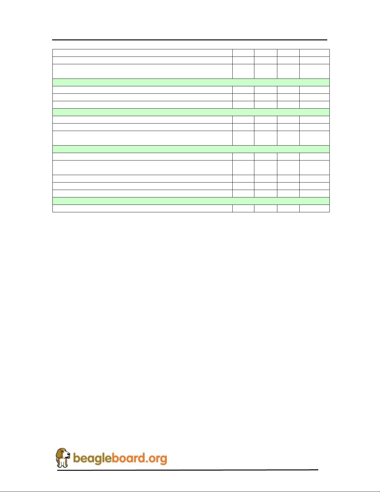
REF: BB_SRM_xM
BeagleBoard-xM System
Reference Manual
Revision C2
High level output voltage
3.3 V
Swing output voltage
400 600
mVp-p
Maximum resolution
1024
x 768
S-Video
Full scale output voltage (75ohm load)
.7
.88 1 V
Offset voltage
50 mV
Output Impedance
67.5
75
82.5
Ohms
Audio In
Peak-to-peak single-ended input voltage (0 dBFs)
1.5
Vpp
Total harmonic distortion (sine wave @ 1.02 kHz @ -1 dBFs)
-80
-75
dB
Total harmonic distortion (sine wave @ 1.02 kHz) 2
0 Hz to 20 kHz, A-weighted audio, Gain = 0 dB
-85
-78
dB
Audio Out
Load Impedance @100 pF
14
16 ohms
Maximum Output Power (At 0.53 Vrms differential output voltage
and load impedance = 16 Ohms)
17.56 mW
Peak-to-Peak output voltage
1.5
Vpp
Total Harmonic Distortion @ 0 dBFs
-80
-75
dB
Idle channel noise (20Hz to 20KHz)
-90
-85
dB
Environmental
Temperature range
0 +85
C
Page 29 of 163
Page 30

REF: BB_SRM_xM
BeagleBoard-xM System
Reference Manual
Revision C2
5.0 Product Contents
Under this section is a description of what comes in the box when the BeagleBoard is
purchased.
5.1 BeagleBoard In the Box
The final packaged -xM Rev C product will contain the following items:
o 1 Box with the following items inside:
o 1 BeagleBoard in an ESD Bag
o 1 uSD card
o 1 uSD Card to MMC Adapter
NO CABLES ARE PROVIDED WITH THE BEAGLEBOARD.
Figure 3. The -xM Rev C Box
Page 30 of 163
Page 31
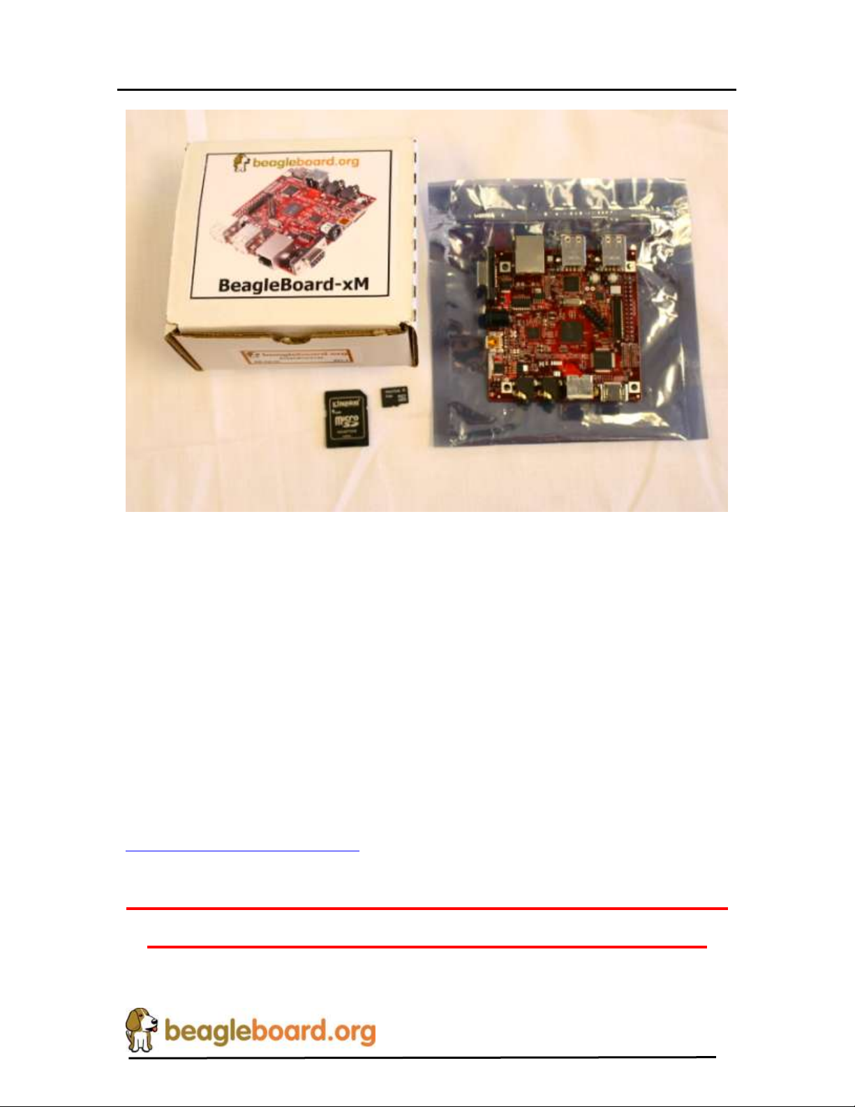
REF: BB_SRM_xM
BeagleBoard-xM System
Reference Manual
Revision C2
Figure 4. -xM Rev C Box Contents
5.2 Software on the BeagleBoard
There is no NAND flash memory on the board so no SW is preinstalled on the board as it
is on the BeagleBoard. The BeagleBoard–xM does come with a 4GB microSD card that
the board boots from. It contains all of the code required for the board to boot to an
Angstrom validation image. You will see a login prompt but no GUI will be visible. It
can also be used to boot to UBoot by hitting a key during the booting process before it
reads the UImage.
5.3 Repairs
If you feel the board is in need of repair, follow the RMA Request process found at
http://beagleboard.org/support/rma
Do not send the board in for repair until a
RMA authorization has been provided.
Page 31 of 163
Page 32

REF: BB_SRM_xM
BeagleBoard-xM System
Reference Manual
Revision C2
Do not return the board to the distributor unless you want to get a refund. You must get
authorization from the distributor before returning the board. Beagleboard.org does not
handle refunds.
6.0 BeagleBoard Connections
This section provides an overview of all of the connectors on the BeagleBoard-xM.
Only the use of FCC Part 15 approved devices in the BeagleBoard-xM installation is
allowed. Care should be taken to insure that all add-on boards, power supplies, monitors,
PC equipment, and any other add-on component or device meets the FCC Part 15
requirements. The user is responsible for compliance with this statement. Any changes or
modifications to this board that causes the board to no longer comply with the FCC Part
15 requirements voids the user’s rights to use this system.
6.1 Connecting USB OTG
The USB OTG port connects to the PC host and uses a miniAB cable through which
power can be provided to the BeagleBoard. Figure 5 shows where the cable is connected
to the BeagleBoard.
If the OTG Port is to be used as a Host, the ID pin must be grounded. This means that
you must have a 5 pin cable connected to the OTG port on the BeagleBoard and you must
use a powered USB HUB. There is also an option to ground the ID on the board and is
discussed later in this document. You can power the board from this port, but there may
not be enough power supplied by the PC to power all features, such as the USB Host
ports and the Ethernet Port. If you use the double ended USB cable, you should be able to
power the board with minimal issues as long as you do not load down the USB Host ports
with heavy current devices. This will depend on the current available from the HOST PC.
Page 32 of 163
Page 33
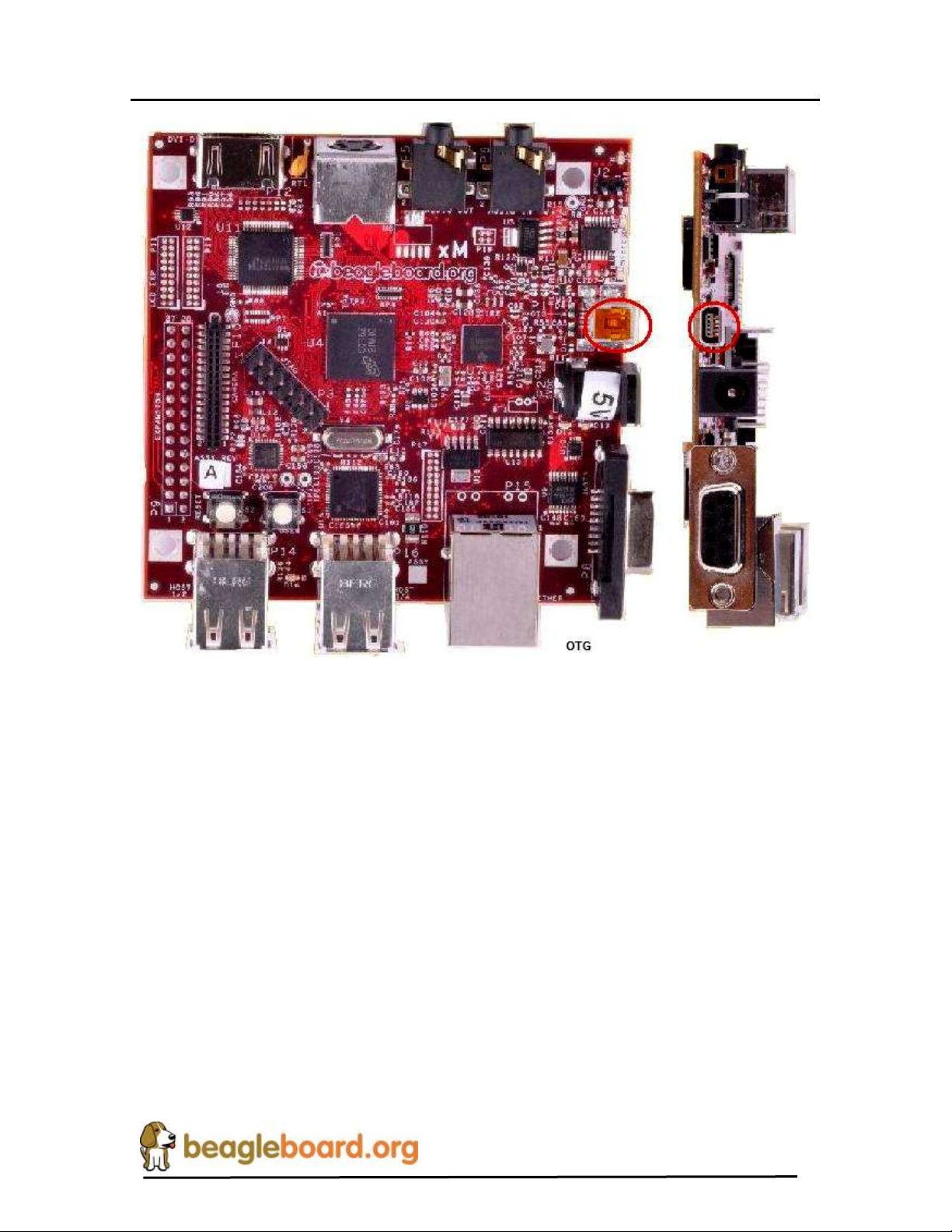
REF: BB_SRM_xM
BeagleBoard-xM System
Reference Manual
Revision C2
Figure 5. USB OTG Connection
Page 33 of 163
Page 34
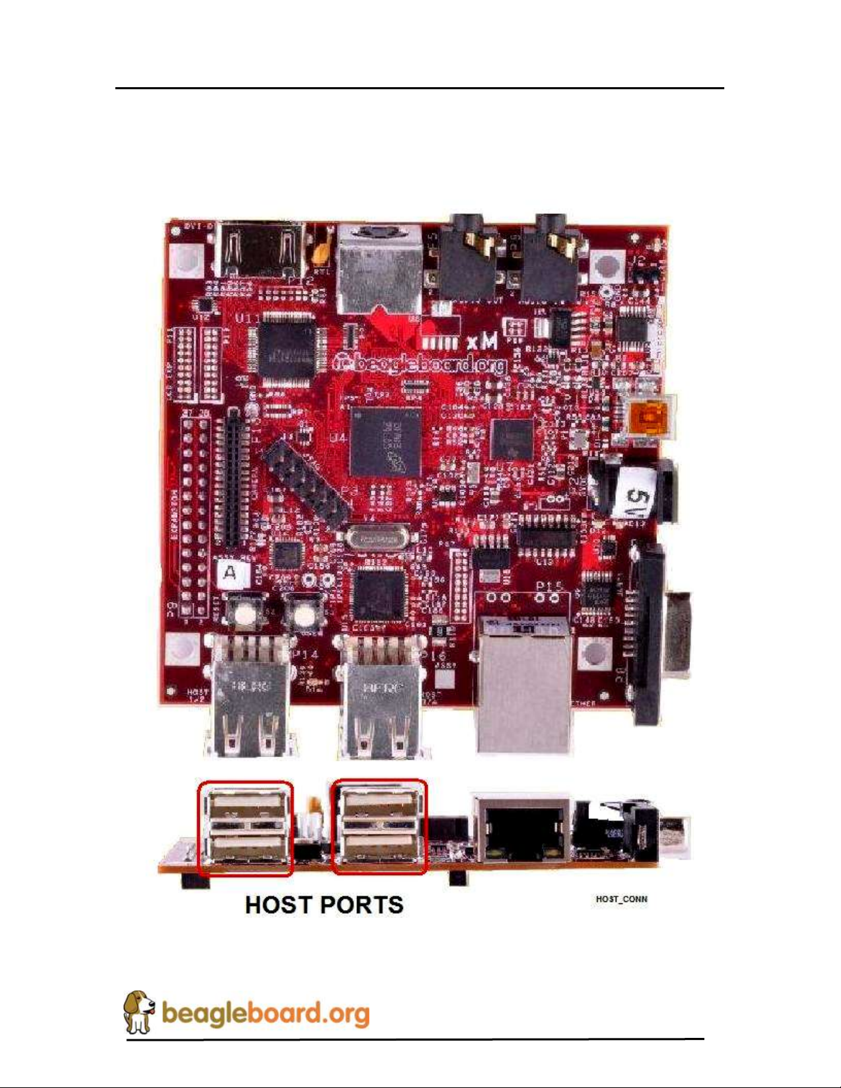
REF: BB_SRM_xM
BeagleBoard-xM System
Reference Manual
Revision C2
6.2 Connecting USB Host
The Beagle is equipped with 4 USB Host connectors. Figure 6 shows the location of the
USB Host connectors.
Figure 6. USB Host Connection
Page 34 of 163
Page 35
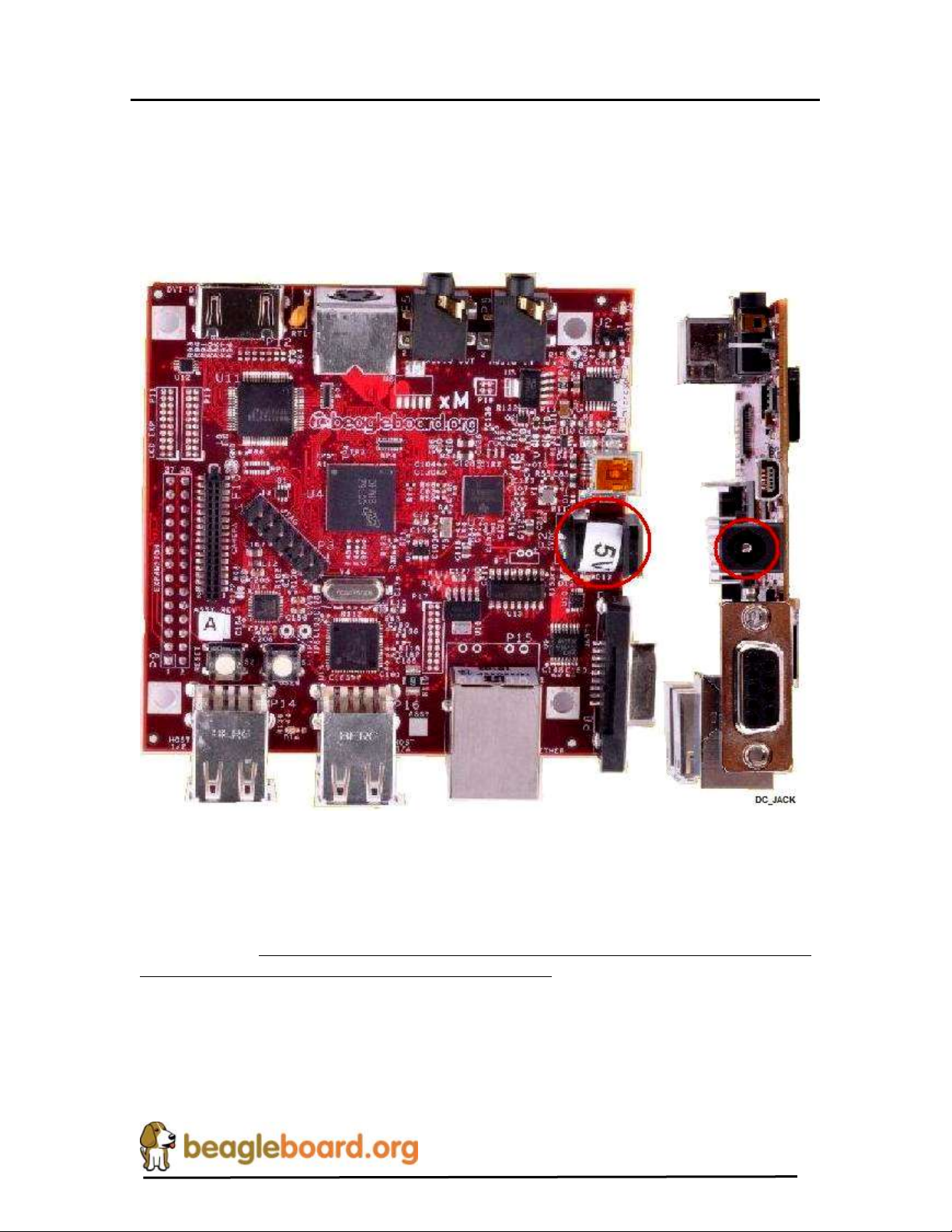
REF: BB_SRM_xM
BeagleBoard-xM System
Reference Manual
Revision C2
6.3 Connecting DC Power
A DC supply can be used to power the BeagleBoard by plugging it into the power jack.
The power supply is not provided with the BeagleBoard, but can be obtained from
various sources. You need to make sure the supply is a regulated 5V supply. Figure 7
shows where to insert the power supply into the power jack.
The power supply must have a 2.1mm I.D x 5.5mm O.D. x 9.5mm and can be either
straight or right angle. Connecting anything other than 5V will activate the over voltage
circuitry, turning on a red LED. The board will not function until the correct power
supply is used. If you are using the USB OTG port in the OTG or host mode, you must
have an external DC supply powering the BeagleBoard.
It is required that on the BeagleBoard-xM board that an external power supply used if
the USB Host is to be used.
Figure 7. DC Power Connection
Page 35 of 163
Page 36
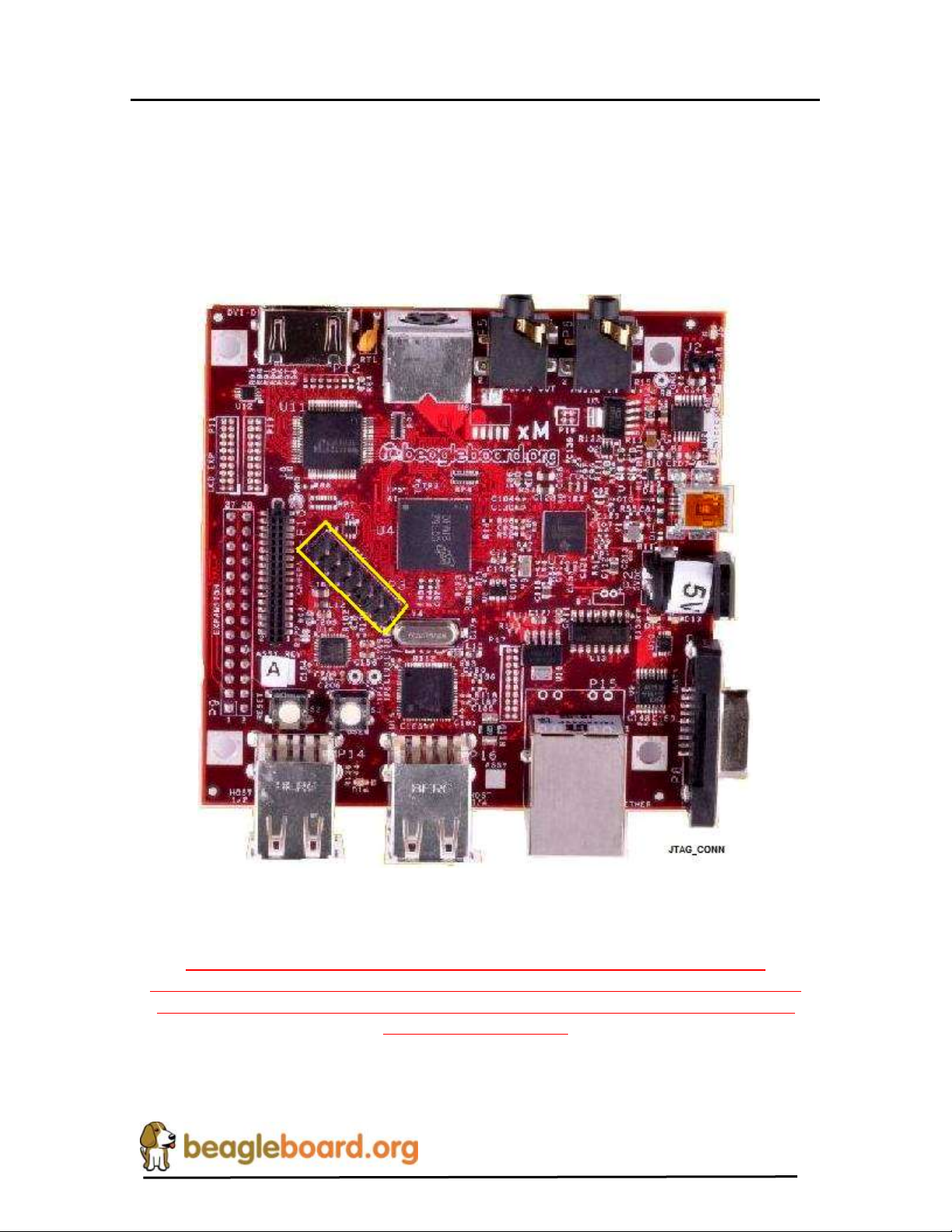
REF: BB_SRM_xM
BeagleBoard-xM System
Reference Manual
Revision C2
6.4 Connecting JTAG
A JTAG emulator can be used for advanced debugging by connecting it to the JTAG
header on the BeagleBoard. Only the 14pin version of the JTAG is supported and if a
20pin version is needed, you will be required to contact your emulator supplier for the
appropriate adapter to be supplied by that manufacturer. Figure 8 shows the connection
of the JTAG cable to the BeagleBoard.
DO NOT expose the JTAG header to 3.3V. It supports 1.8V only. There is no
overvoltage protection on these pins and the pins connect direct to the processor. If you
do this, the board will be damaged beyond repair and the board will NOT be replaced
Figure 8. BeagleBoard JTAG Connection
under any circumstances
Page 36 of 163
Page 37
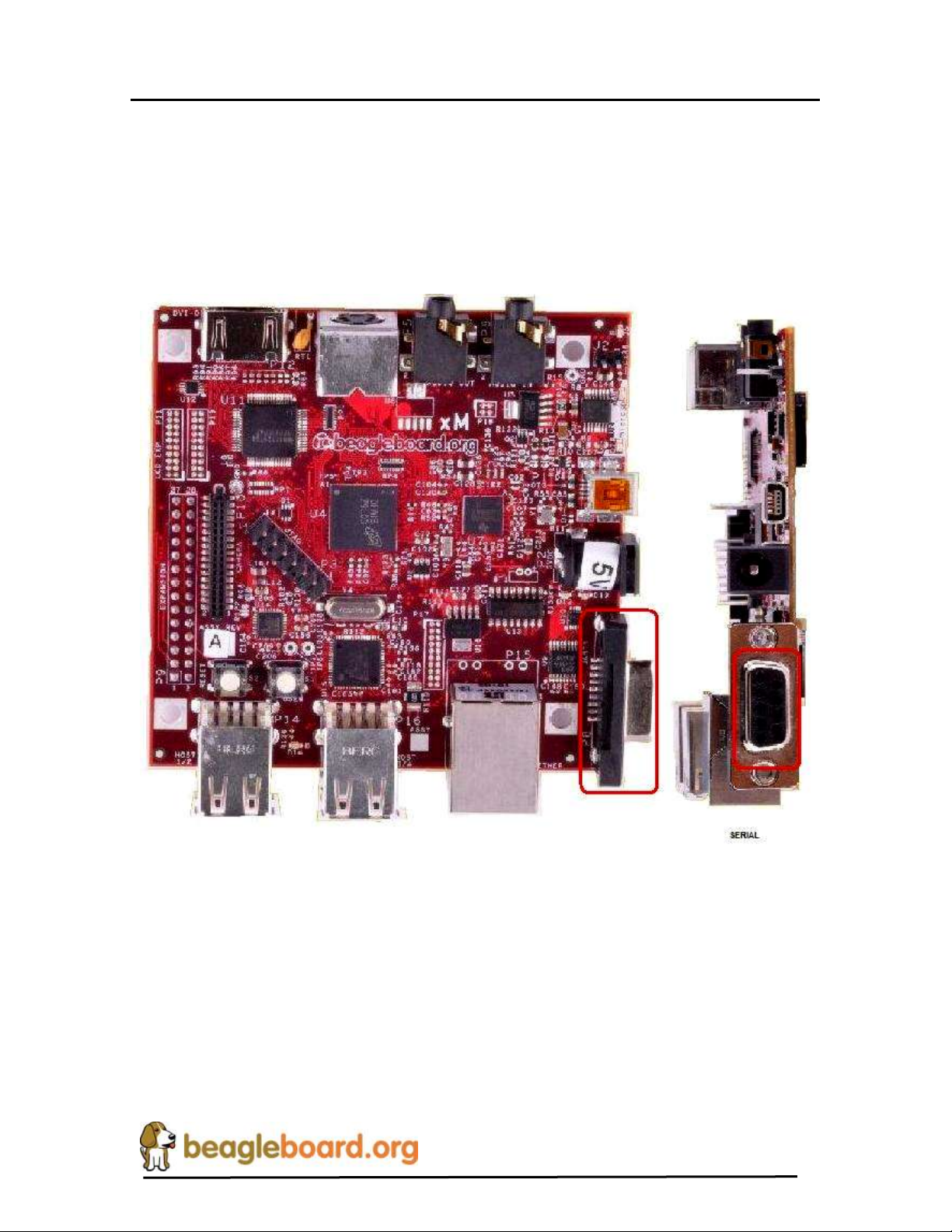
REF: BB_SRM_xM
BeagleBoard-xM System
Reference Manual
Revision C2
6.5 Connecting Serial Cable
In order to access the serial port of the BeagleBoard a serial cable is required. New to the
BeagleBoard-xM version is the removal of the 10 pin header and the addition of a female
DB9 connector. The configuration of the DB9 is such that a USB to serial adapter can be
plugged direct into the Beagle connector. No null modem cable is required. Figure 9
shows where the serial cable is to be installed.
If you are using a standard serial port on the PC, a straight through male to female cable
is required. The cable used on the BeagleBoard will not work on the BeagleBoard–xM
board.
Figure 9. BeagleBoard Serial Cable Connection
Page 37 of 163
Page 38
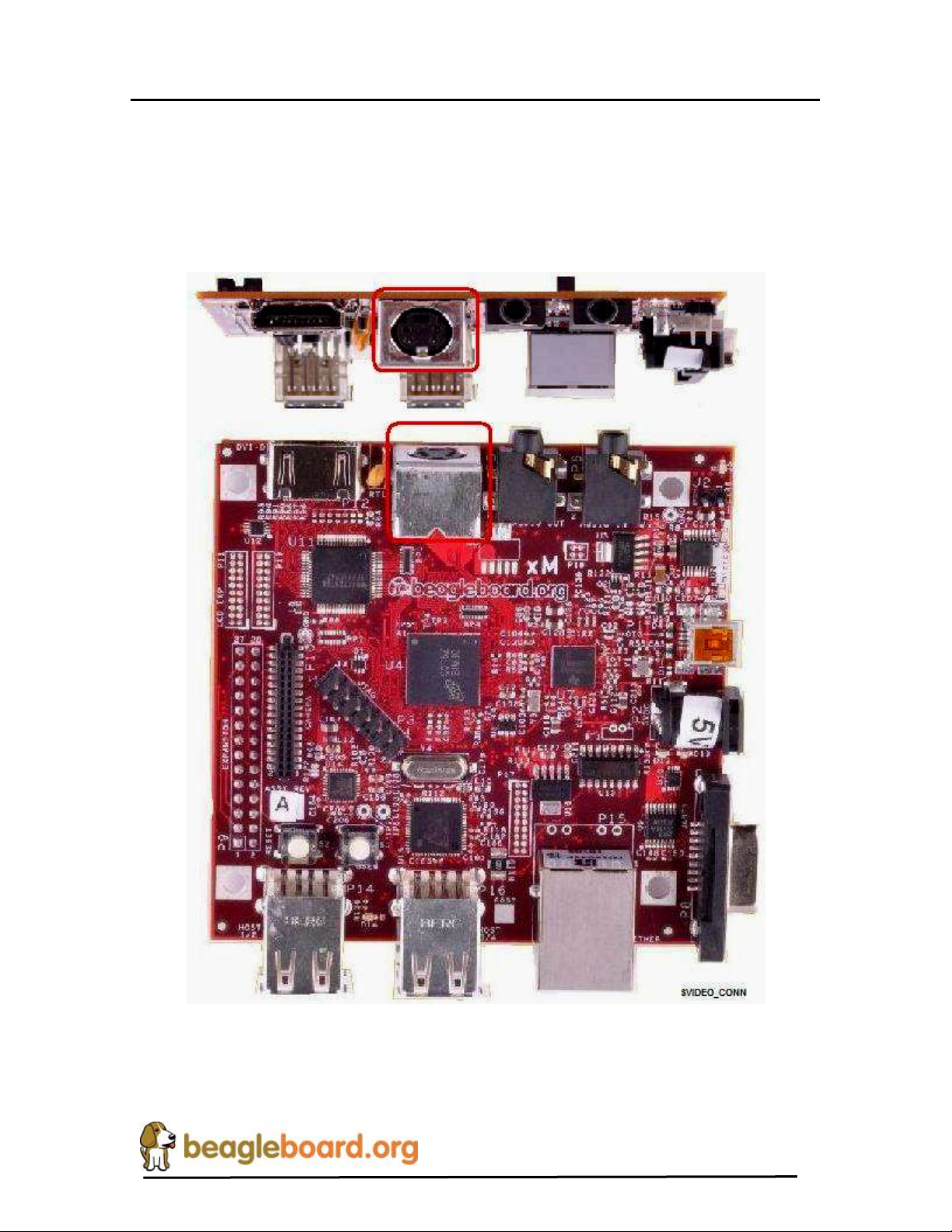
REF: BB_SRM_xM
BeagleBoard-xM System
Reference Manual
Revision C2
6.6 Connecting S-Video
An S-Video cable can be connected to the BeagleBoard and from there it can be
connected to a TV or monitor that supports an S-Video input. This cable is not supplied
with the BeagleBoard. Figure 10 shows the connector for the S-Video cable.
Figure 10. BeagleBoard S-Video Connection
Page 38 of 163
Page 39
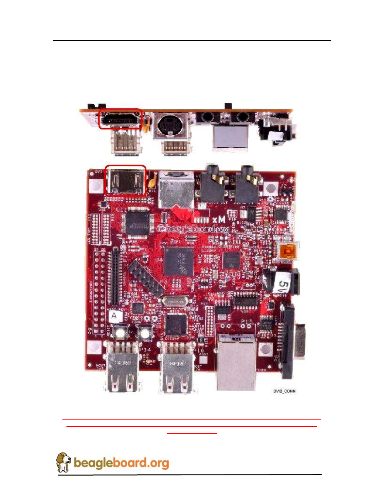
REF: BB_SRM_xM
BeagleBoard-xM System
Reference Manual
Revision C2
6.7 Connecting DVI-D Cable
In order to connect the DVI-D output to a monitor, a HDMI to DVI-D cable is required.
This cable is not supplied with BeagleBoard but can be obtained through numerous
sources. Figure 11 shows the proper connection point for the cable.
DO NOT PLUG IN THE DVI-D CONNECTOR TO A DISPLAY WITH THE BEAGLEBAORD
POWERED ON. PLUG IN THE CABLE TO THE DISPLAY AND THEN POWER ON THE
Figure 11. BeagleBoard DVI-D Connection
BEAGLEBOARD.
Page 39 of 163
Page 40
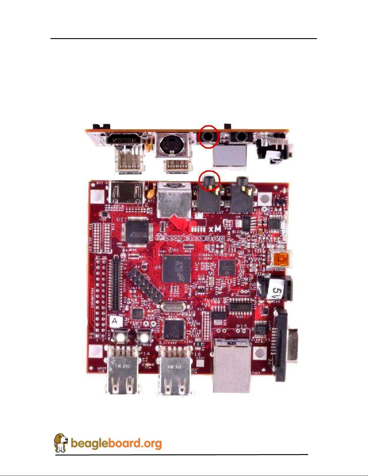
REF: BB_SRM_xM
BeagleBoard-xM System
Reference Manual
Revision C2
6.8 Connecting Stereo Out Cable
An external Audio output device, such as external stereo powered speakers, can be
connected to the BeagleBoard via a 3.5mm jack. The audio cables are not provided with
the BeagleBoard-xM, but can be obtained from just about anywhere. Figure 12 shows
where the cable connected to the stereo out jack.
Figure 12. BeagleBoard Audio Out Cable Connection
Page 40 of 163
Page 41
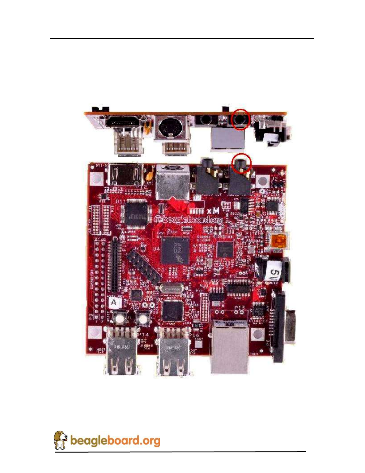
REF: BB_SRM_xM
BeagleBoard-xM System
Reference Manual
Revision C2
6.9 Connecting Stereo In Cable
External Audio input devices, such as a powered microphone or the audio output of a PC
or MP3 player, can be connected to the BeagleBoard-xM via a 3.5mm jack. The audio
cables are not provided with the board, but can be obtained from several sources. Figure
13 shows where the cable is connected to the stereo input jack.
Figure 13. BeagleBoard Audio In Cable Connection
Page 41 of 163
Page 42
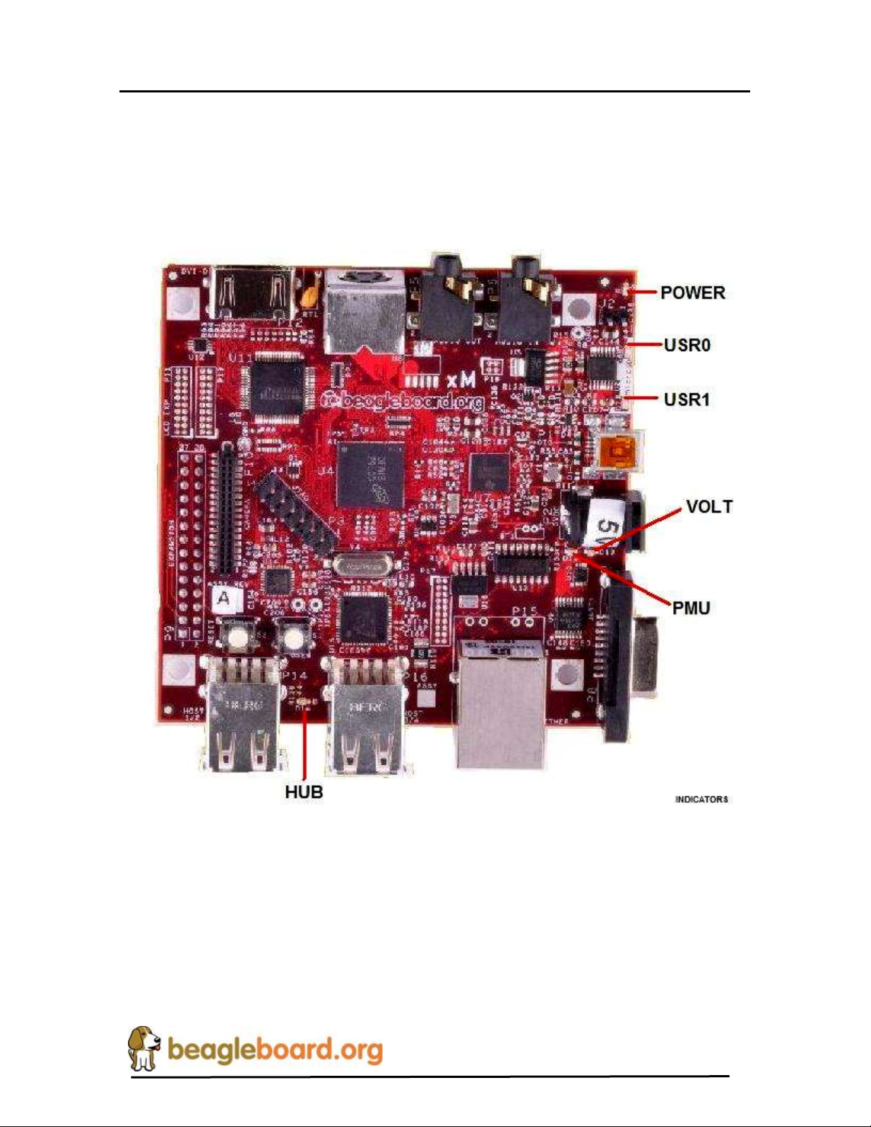
REF: BB_SRM_xM
BeagleBoard-xM System
Reference Manual
Revision C2
6.10 Indicator Locations
There are five green and one red indicator on the BeagleBoard. Figure 14 shows the
location of each indicator. Each indicator will be described in more detail later in this
document.
POWER indicates that power is applied to the board.
USR0/1 can be used by the SW as needed
PMU is controlled from the power management chip and can be connected to a PWM.
VOLT will turn on when the DC voltage exceeds specification
HUB turns on when power is applied to the USB HUB.
Figure 14. BeagleBoard Indicator Locations
Page 42 of 163
Page 43
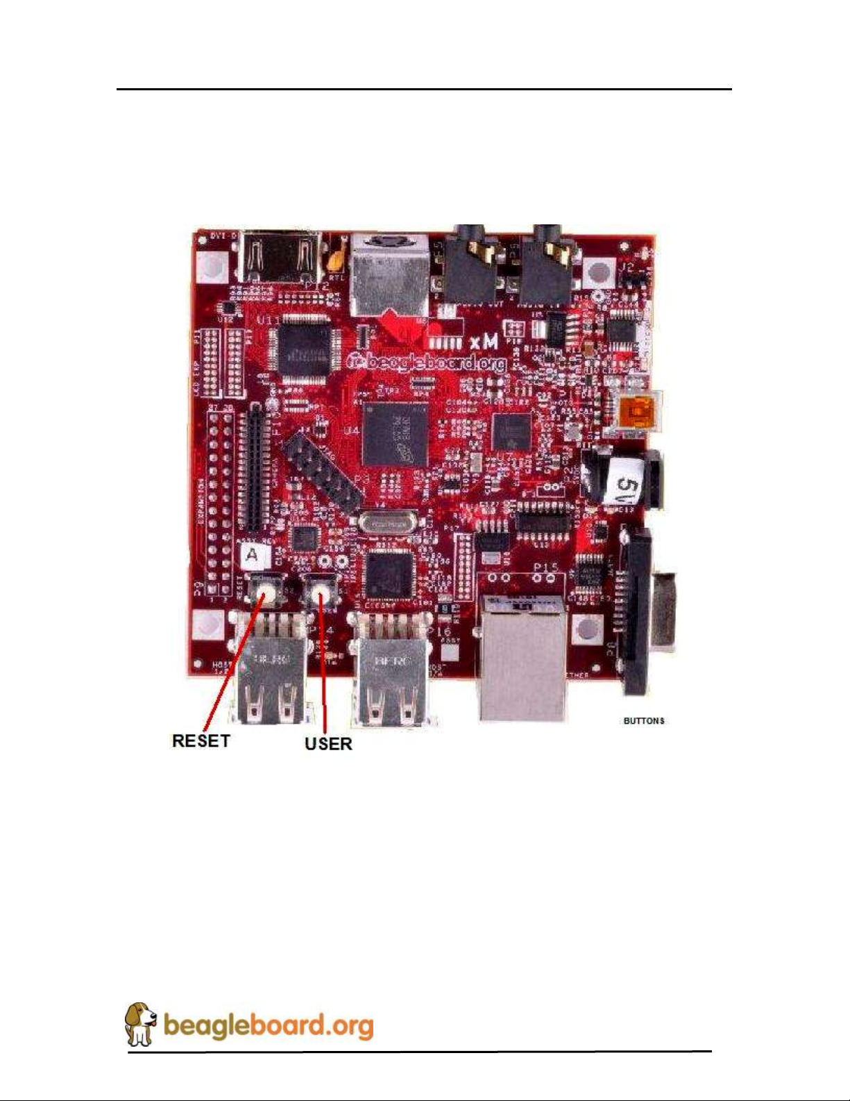
REF: BB_SRM_xM
BeagleBoard-xM System
Reference Manual
Revision C2
6.11 Button Locations
There are two buttons on the BeagleBoard-xM; the RESET button when pressed will
force a board reset and the USER button which can be used by the SW for user
interaction. Figure 15 shows the location of the buttons.
The User button does no affect the boot source of the board as is the case on the
BeagleBoard version. If you do press the User Button on power up, the board will not
boot.
Figure 15. BeagleBoard Button Location
Page 43 of 163
Page 44
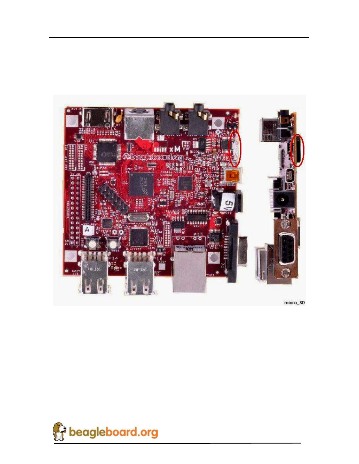
REF: BB_SRM_xM
BeagleBoard-xM System
Reference Manual
Revision C2
6.12 microSD Connection
The microSD is the boot source for the board. It uses a push-push connector for the
insertion and removal of the microSD card. The connector is mounted on the bottom side
of the board. Figure 16 shows the location of the microSD connector.
The microSD card should be inserted with the writing on the card facing up. The white
silkscreen area on top of the board works as a guide to align the card for insertion.
Figure 16. BeagleBoard microSD Card Location
Page 44 of 163
Page 45
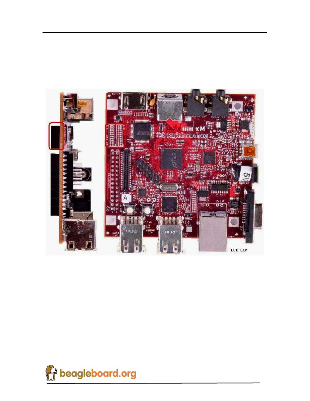
REF: BB_SRM_xM
BeagleBoard-xM System
Reference Manual
Revision C2
6.13 LCD Connection
There are two headers provided to access the LCD signals on the BeagleBoard-xM.
These headers are 2x10 headers with a spacing of .05 (1.27mm) pitch. How these
connectors are used is determined by the design of the adapter board that is connected to
them. Figure 17 shows the location of the LCD headers on the board.
Adapter boards are becoming available for such things as LCD panels and VGA adapters.
As different LCD panels have different requirements, it is difficult to design an interface
that will work with all LCD panels. That is the reason only the raw signals are brought
out on these headers.
Figure 17. BeagleBoard LCD Header Location
Page 45 of 163
Page 46
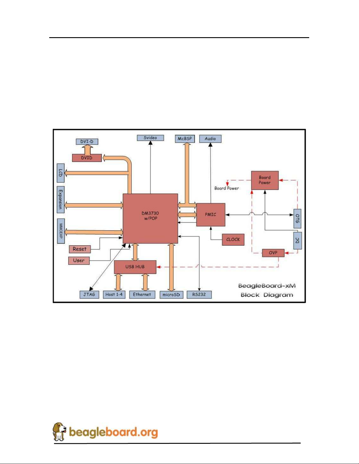
REF: BB_SRM_xM
BeagleBoard-xM System
Reference Manual
Revision C2
7.0 BeagleBoard-xM System Architecture and Design
This section provides a high level description of the design of the BeagleBoard-xM and
its overall architecture.
7.1 System Block Diagram
Figure 18 is the high level block diagram of the BeagleBoard-xM.
Figure 19 shows the location of the key components on the board.
Figure 18. BeagleBoard-xM High Level Block Diagram
Page 46 of 163
Page 47
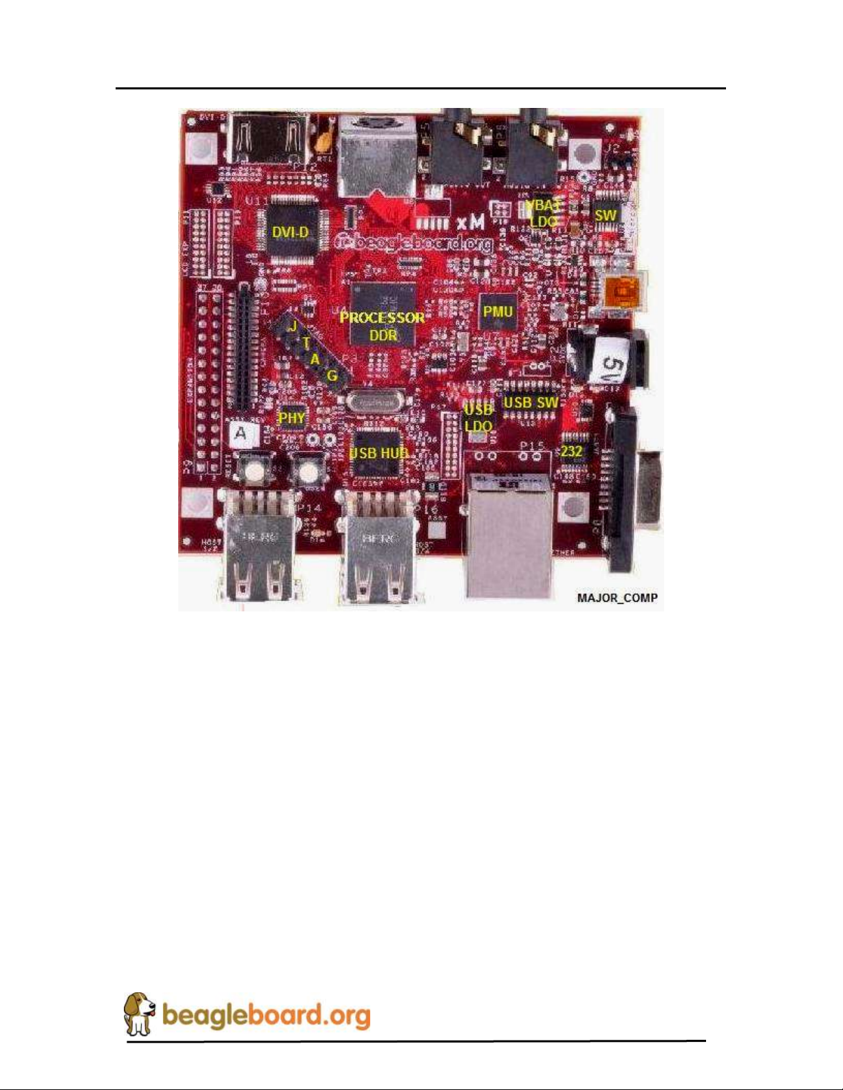
REF: BB_SRM_xM
BeagleBoard-xM System
Reference Manual
Revision C2
Figure 19. BeagleBoard Major Components
The information found in the remainder of this section describes in detail the architecture
and design of the BeagleBoard-xM.
You will notice certain things in this section.
o The schematic has been created for each section showing only the pertinent
components and their connections.
o The pin names differ from the actual schematic. For ease of reading, the names
have been truncated to only show the specific functions of that pin as used in the
design.
Page 47 of 163
Page 48
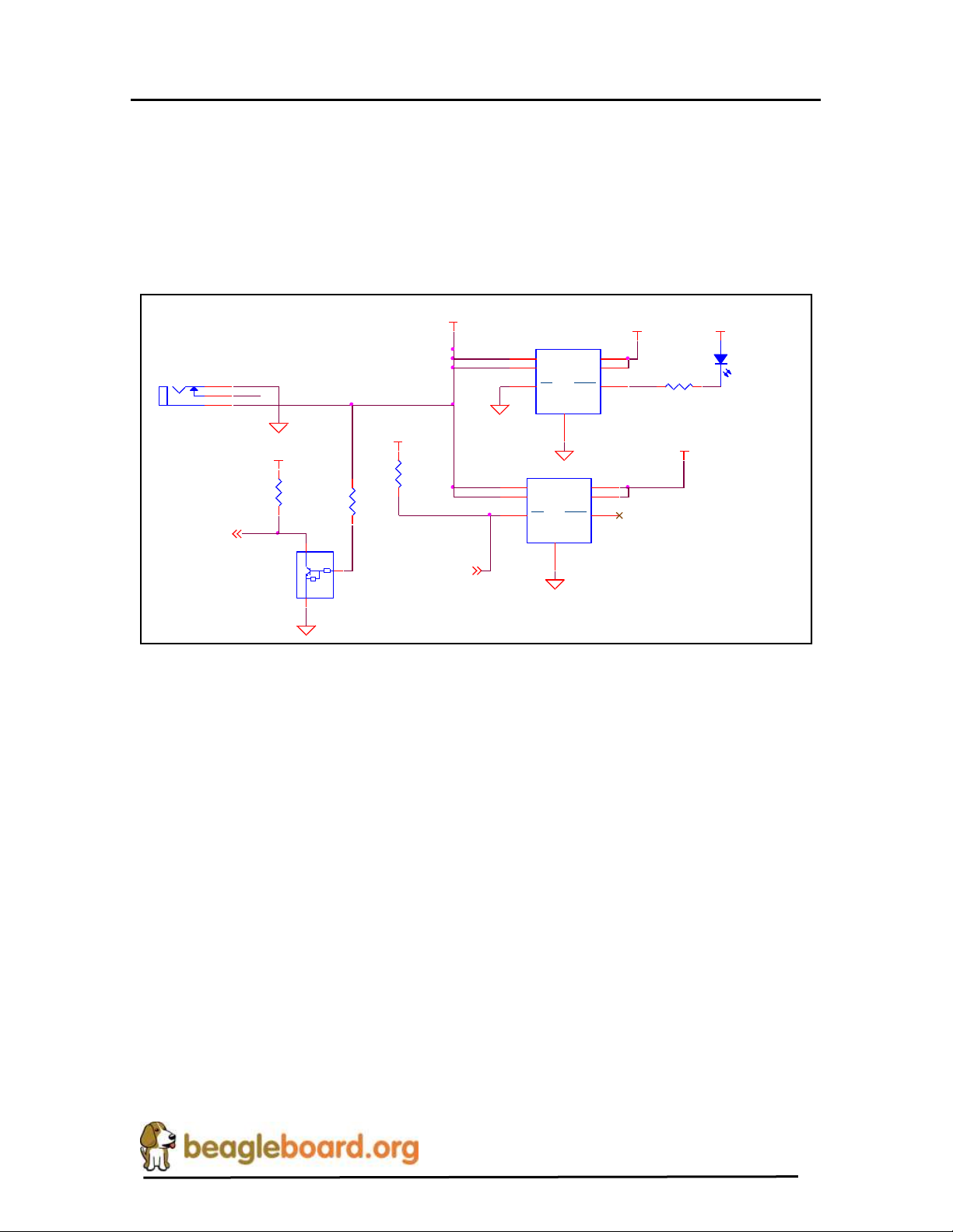
REF: BB_SRM_xM
BeagleBoard-xM System
Reference Manual
Revision C2
RED
D13
LTST-C150CKT
R138
10K
DC_I N
DC_5V
P2
CONN _PWR1_2. 5MM
2
3
1
R144
10K
nDC_PW R6
VIO_1V8
R121
510
DC_I N
On powerup, USB Host
circutry power is OFF.
VIO_1V8
R131
10K
nUSBHOST_PWR _EN6
U33
NCP349MNAE
IN0
7
IN11OUT0
4
OUT1
5
EN
6
GND
2
FLAG
3
DC_5V_U SB
U31
NCP349MNAE
IN0
7
IN11OUT0
4
OUT1
5
EN
6
GND
2
FLAG
3
47k
10k
Q2A
RN1907
1 6
2
7.2 Over Voltage Protection
A new feature found on the BeagleBoard–xM board is the overvoltage protection circuit.
The design of this circuit has been changed on the Rev C version of the board and is
much simpler and more affective. The primary function of this circuit it to prevent
voltage levels in excess of the specification from reaching other circuitry on the board
and causing damage to the board. Figure 20 is the diagram of the circuitry design.
These functions are controlled by the NCP349 device. The NCP349 provides
overvoltage protection for positive voltage, up to 28V. A low NMOSFET protects the
systems connected on the OUT0/1 pins against positive overvoltage. At power up, with
EN pin = low, the output is delayed before it is turned on to insure that the voltage is not
in excess of 5.8V. The NCP349 provides a FLAG output, which alerts the system that a
fault has occurred by turning on D13, a red LED. The board will not power up if the
voltage is in excess of the 5.8V max level.
Also new in the REV C is the fact that the USB 5V defaults to off, making sure that the
voltage is not connected to the USB power FET. We were seeing a small number of
boards that still had this device sustaining damage. This was the reason for the circuit
design change. Having this default to off provides an additional level of protection.
New to the Rev C as well, is the ability to detect when the board is DC powered by
reading the nDC_PWR signal. This is useful to allow the SW to determine that if in the
OTG power mode, that the USB Host ports are not available.
Also new for the Rev C is the ability to power the HUB for the USB OTG port. As U31
is always on, connecting power via the OTG port provided 5V to the DC_5V rail which
Figure 20. Overvoltage Protection
Page 48 of 163
Page 49

REF: BB_SRM_xM
BeagleBoard-xM System
Reference Manual
Revision C2
in turn will supply power to the DC in rail which can then be used to power the HUB as
long as U33 is enabled.
7.3 Power Conditioning
There are two possible sources of the 5V required by the BeagleBoard. It can come from
the USB OTG port connected to a PC or a 5V DC supply. The USB supply is sufficient
to power the BeagleBoard in most as long as you understand that the USB Host ports will
not function. It is recommended that a DC supply be used.
It should also be noted that if an OTG configuration is used, for example tying two
BeagleBoards together via a UBS OTG cable, both of the BeagleBoards must be powered
by the DC supply. If the OTG port is used as a Host port, then the DC supply must also
be used. Figure 21 is the design of the main power input section.
Page 49 of 163
Page 50
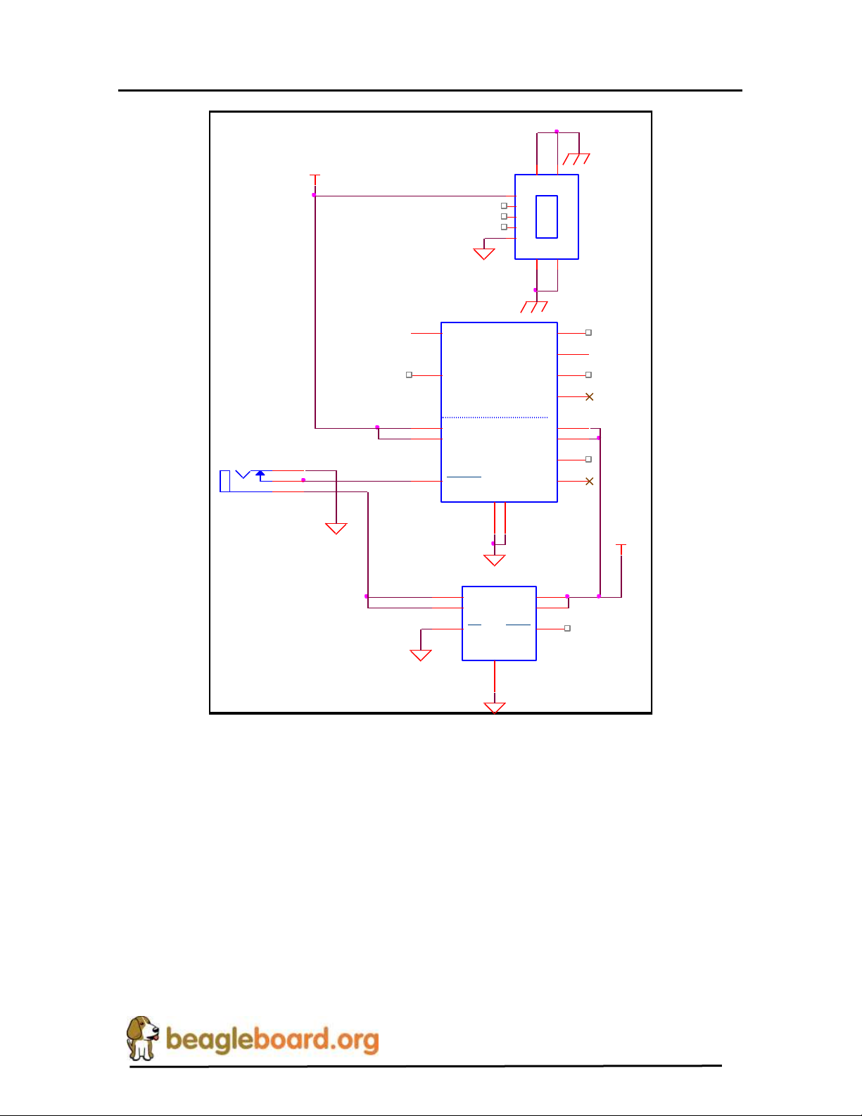
REF: BB_SRM_xM
BeagleBoard-xM System
Reference Manual
Revision C2
P20
mini USB-AB
D-
2
D+
3
VB
1
ID
4
G27G3
6
G1
5
G5
8G49
P21
CON N_PW R1_2. 5MM
2
3
1
U6
TPS2141PWP
LDO_IN
4
LDO_EN
6
SW_IN
2
GND
7
LDO_PLDN
10
LDO_OU T
11
ADJ
9
LDO_PG
8
SW_OU T
12
SW_PLDN
14
SW_PG
1
SW_EN
5
SW_IN
3
SW_OU T
13
PPAD
15
VBUS_5V0
DC_5V
U34
NCP349MNAE
IN0
7
IN11OUT0
4
OUT1
5
EN
6
GND
2
FLAG
3
7.3.1 USB DC Source
The USB specification requires that the current consumed prior to enumeration be limited
to 100mA @ 5V (500mW). The 5V DC from the USB is routed through the TPS2141
switch to insure that this requirement is met as uncharged capacitors on the BeagleBoard
can exhibit a large current drain during start up that could exceed this requirement. The
TPS2141 is a USB 2.0 Specification-compatible IC containing a dual-current limiting
power switch and an adjustable low dropout regulator (LDO). Both the switch and LDO
limit inrush current by controlling the turn on slew rate. The dual-current-limiting feature
of the switch allows USB peripherals to utilize high-value capacitance at the output of the
switch, while keeping the inrush current low.
Figure 21. Input Power Section
Page 50 of 163
Page 51

REF: BB_SRM_xM
BeagleBoard-xM System
Reference Manual
Revision C2
During turn on, the switch limits the current delivered to the capacitive load to less than
100 mA. When the output voltage from the switch reaches about 93% of the input
voltage, the switch current limit increases to 800mA (minimum), at which point higher
current loads can be turned on. The higher current limit provides short circuit protection
while allowing the peripheral to draw maximum current from the USB bus.
When in the USB powered mode and no DC supply is connected, the TPS2141 is
enabled, allowing the power to be supplied to the board from the OTG port through the
integrated switch inside the TPS2141.
7.3.2 Wall Supply Source
A wall supply can be used to provide power to the board. A regulated 5V DC supply of at
least 2A is required and a rating of 3A is preferred, assuming that the USB ports and
expansion headers are likely to be used. It needs to have a 2.1mm plug with a center hot
configuration. If you are using the USB HUB or Ethernet interface, additional current is
required. In the event that a higher DC load is required due to the addition of a
Daughtercard or if all the USB host ports need to supply the full 500mA per port, a
higher current supply can be used. The maximum current should not exceed 3A.
7.3.3 DC Source Control
Unlike when powering from the USB OTG port, in the case of the DC voltage, the
current limiting is not required. As long as the DC supply is not connected, the switch for
the USB is enabled. When the DC supply is plugged in, the switch is disabled because the
ground is removed from pin 5 of the TPS2141. This insures that the 5V from the USB is
not connected by disabling the internal FET. In the case where there is no USB plugged
in, there is no 5V available to be routed so the removal of the pullup in pin 5 has no
affect.
When in the DC mode of operation, the USB OTG can be used in the Host or Client
modes. The TPS65950 will be responsible for handling the supply of the VBUS_5V0 rail
in the OTG or Host modes. As this is limited to 100mA, a powered hub must be used to
support peripherals on the OTG port.
It is possible to provide 5V via the expansion connectors as would be the case from a
daughter card to prevent you from having to have two DC supplies. You should be
careful in doing this. If you plan to use the USB OTG port, you will need to place an
unconnected connector into the DC power jack to insure that the DC from the OTG port
is not shorted to the 5V supplied via the expansion connector. There is a signal called
nUSB_PWR which if a logic level “1” (5V) indicates that there is 5V supplied by the
USB OTG port, it is plugged in, and the DC dummy jack is installed. This condition
could be used on the daughtercard to know that it is OK to supply power onto the
expansion bus to power the board. If this signal is low, then that indicates that there is no
Page 51 of 163
Page 52
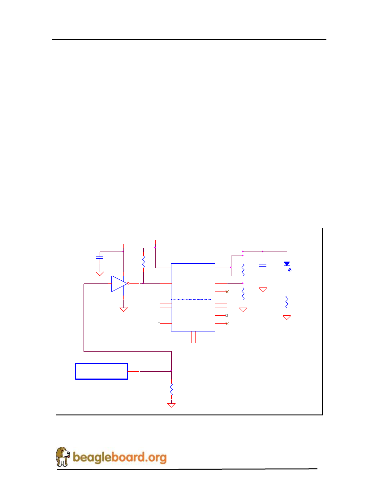
REF: BB_SRM_xM
BeagleBoard-xM System
Reference Manual
Revision C2
R9
620K,1%,0603
R12
330
GRN
D5
LTST-C190GKT
AUX_3V3
R10
200K,1%,0603
PWRLED _R
U18A
SN74LVC2G06D CKR
1
2 5
6
C204
0.1uF, 10V
VIO_1V8
POWER
3V3_ADJ
U2
TPS2141PWP
LDO_IN
4
LDO_EN
6
SW_IN
2
GND
7
LDO_PLDN
10
LDO_OUT
11
ADJ
9
LDO_PG
8
SW_OUT
12
SW_PLDN
14
SW_PG
1
SW_EN
5
SW_IN
3
SW_OUT
13
PPAD
15
VBAT
C207
4.7uF, 6.3V, 0603
R8
10K
R54
10K
U7A TPS65950
GPIO.1/ CD 2/JTAG.TMS
N12
DC power connected and there is no USB OTG port connected. For this reason, is
recommended however, that a large pullup be provided on the daughtercard to make the
signal a logic level “1” (5V) to detect the true state of the DC jack. It is always possible
that at any point a USBOTG cable could be installed. This means that in order to power
the board from the expansion headers, the DC dummy jack must be installed and there is
a method to verify that condition.
7.3.4 AUX 3.3V Supply
The TPS2141 has an integrated 3.3V LDO which is being used to supply the 3.3V as
required on the BeagleBoard for the DVI-D interface and the UART. The input to the
LDO is supplied by the main DC_5V. This insures that the power to the LDO can be
supplied by either the USB or the DC wall supply and that the current measurement
includes the 3.3V supply. The 3.3V supply can be turned off by activating GPIO1 on the
TPS65950 to a 1. By default the voltage is on. You will also see that the 3.3V supply
powers the power LED, D5. If during a low power mode, the user chooses to turn of the
power LED, this GPIO pin can be used to turn off the power LED. It should also be
noted, that the 3.3V rail controls the serial port power, so this will be powered down as
well. Figure 22 is the AUX 3.3V Supply design.
Figure 22. AUX 3.3 Power Section
Page 52 of 163
Page 53
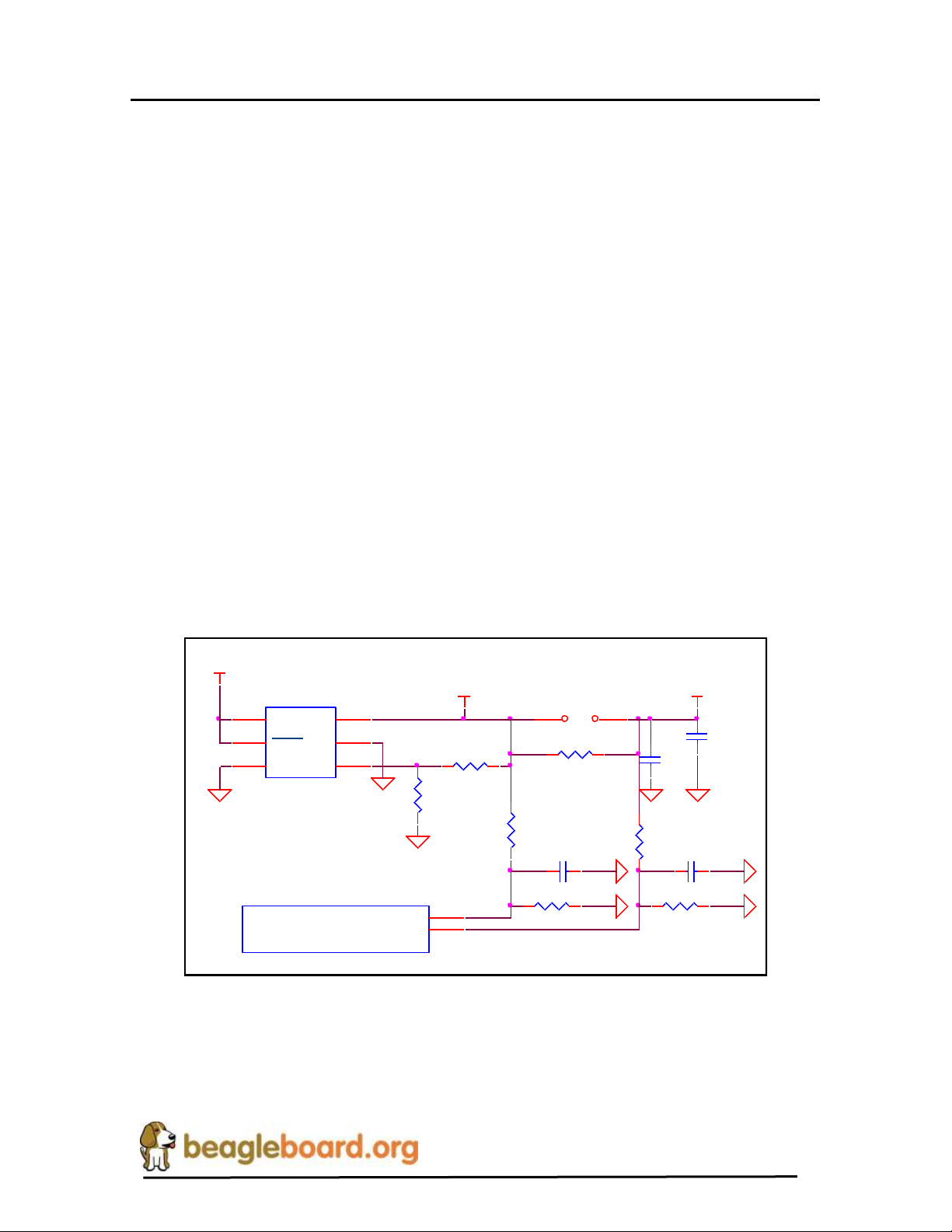
REF: BB_SRM_xM
BeagleBoard-xM System
Reference Manual
Revision C2
C83 0.1uF,10V
R52
10K,1%
C84 0.1uF,10V
R53 10K,1%
ADCIN5
ADCIN3
R48
12K,1% R49
12K,1%
VBAT_FB
VBAT
R14
56.2K,1%
R15
22.6K,1%
C5
10uF,C ER, 0805,6. 3V
DC_5V
4.2V
VBAT_MAI N
C7
0.1uF, 10VR13 .1,0805
+
J2
HDR2_.1x .1
1 2
U3
TL1963A
IN
2
SHDN
1
OUT
4
ADJ
5
GND
3
GND
6
U7A TPS65950
CTSI/BER DATA/AD CIN3
P11
RTSO/CLK64K/ BERC LK/ADCIN 5
N11
7.4 Meter Current Measurement
Jumper J2 is a header that allows for the voltage drop across the resistor to be measured
using a meter, providing a way to measure the current consumption of the BeagleBoard
from the main voltage rails, either USB or DC. The resistor, R13, is a .1 ohm resistor
across which the voltage is measured. The reading you get is .1mV per mA of current.
You will need to make sure you have a sensitive meter to make your measurements.
Please keep in mind, that this current reading does not include any current consumed by
the USB HUB, USB ports, or the Expansion headers.
7.5 Processor Current Measurement
The resistor across J2 can also be used to measure the current of the board by reading the
voltage drop across R13 from software. There are two pairs of resistors provided on the
TPS65950 that measure the voltage on either side of R13. This is done via the I2C
control bus to the TPS65950 from the processor. These values along with resistance of
R13 are used to calculate the current consumption of the board. Figure 24 is the
schematic of the measurement circuitry. The maximum value that can be input to the
ADC inputs is based on the setting of the VINTANA2.OUT voltage rail which defaults
to 2.5V. In order to prevent the voltage levels from exceeding this value a pair of resistors
of 12K and 10K is used to scale the voltage down.
This results in a value that is 46% of the actual value. So, for a maximum value of 5.25V,
the voltage read would be 2.415V which keeps it below the 2.5V point. The voltage drop
across R13 will be small as the value of the resistor is 0.1 ohms. For every 100 mA of
Figure 23. Processor Current Measurement
Page 53 of 163
Page 54

REF: BB_SRM_xM
BeagleBoard-xM System
Reference Manual
Revision C2
current a voltage of .01V will be detected. In order to determine the actual power, the
input voltage and the voltage drop must be measured.
Page 54 of 163
Page 55
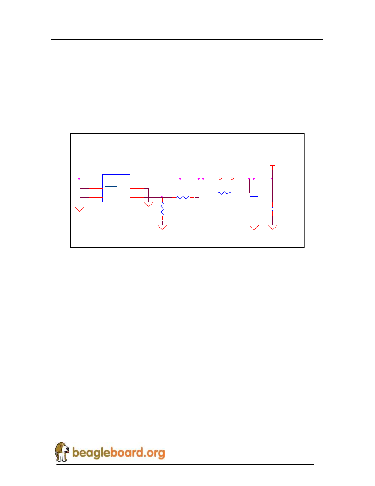
REF: BB_SRM_xM
BeagleBoard-xM System
Reference Manual
Revision C2
VBAT_FB
VBAT
R14
56.2K,1%
R15
22.6K,1%
C5
10uF,C ER, 0805,6. 3V
DC_5V
4.2V
VBAT_MAI N
R13 .1,0805
C7
0.1uF, 10V
+
J2
HDR2_.1x .1
1 2
U3
TL1963A
IN
2
SHDN
1
OUT
4
ADJ
5
GND
3
GND
6
7.6 VBAT Power Conditioning
This circuitry regulates the DC input to a nominal 4.2VDC level. This is required in order
to meet the maximum DC voltage level as specified by the TPS65950 Power
Management device which is 4.7V. Using 4.2V gives us some margin and meets the
nominal 4.2V rating of the TPS65950.
Figure 25 is the power conditioning section of the BeagleBoard.
Figure 24. VBAT Power Conditioning
The TPS65950 provides the main power rails to the board and has a maximum limit of
4.7V on its VBAT input and a nominal of 4.2V. U3, the TL1963A, is used to convert the
DC_5V, which can come from a DC wall supply or the USB, to 4.2V to meet this
requirement. The TL1963A is a linear low-dropout (LDO) voltage regulator and is
thermal shutdown and current limit protected. It has the ability to deliver 1A of current,
although this is far and above the requirements of the board. By adjusting the values of
R14 and R15, the actual voltage can be adjusted if needed.
7.7 TPS65950 Reset and Power Management
The TPS65950 supplies several key functions on the BeagleBoard. This section covers a
portion of those functions centered on the power and reset functions. Included in this
section are:
o Main Core Voltages
o Peripheral Voltages
o Power Sequencing
o Reset
Page 55 of 163
Page 56

REF: BB_SRM_xM
BeagleBoard-xM System
Reference Manual
Revision C2
o Current measurement via SW
The other functions are covered in other sections in this document and are grouped by
their overall board functions. The explanation of the various regulators found on the
TPS65950 is based upon how they are used in the board design and are not intended to
reflect the overall capability of the TPS65950 device. Please refer to the TPS65950
documents for a full explanation of the device operation.
7.7.1 Main Core Voltages
The TPS65950 supplies the three main voltage rails for the processor and the board:
o VDD1 (1.2V, adjustable)
o VDD2 (1.3V)
o VIO_1V8 (1.8V)
The VOCORE_1V3 defaults to 1.2V at power up, but can be adjusted by software to the
1.3V level. Figure 26 is the interfacing of the TPS65950 to the system as it provides the
three main rails.
7.7.2 Main DC Input
The main supply to the TPS65950 for the main rails is the VBAT rail which is a nominal
4.2V. Each rail has a filter cap of 10uF connected to each of the three inputs. A .1uF cap
is also provided for high frequency noise filtering.
7.7.3 Processor I2C Control
The various components in the TPS65950 are controlled from the processor via the I2C
interface. I2C_0 is used to control the TPS65950 device.
7.7.4 VIO_1V8
The VIO_1V8 rail is generated by the TPS65950 VIO regulator. The VIO output is a
stepdown converter with a choice of two output voltage settings: 1.8 V or 1.85 V. The
voltage is set by configuring the VSEL bit (VIO_VSEL[0]). When the VSEL bit is set to
0, the output voltage is 1.8 V, and when it is set to 1, the output voltage is 1.85 V.
When the TPS65950 resets, the default value of this LDO is 1.80 V; the processor must
write 1 to the VSEL field to change the output to 1.85 V. The default for the BeagleBoard
is 1.8V. This regulator output is used to supply power to the system memories and I/O
ports. It is one of the first power supplies to be switched on in the power-up sequence.
VIO does not support the SmartReflex voltage control schemes. VIO can be put into
sleep or off mode by configuring the SLEEP_STATE and OFF_STATE fields of the
VIO_REMAP register.
Page 56 of 163
Page 57
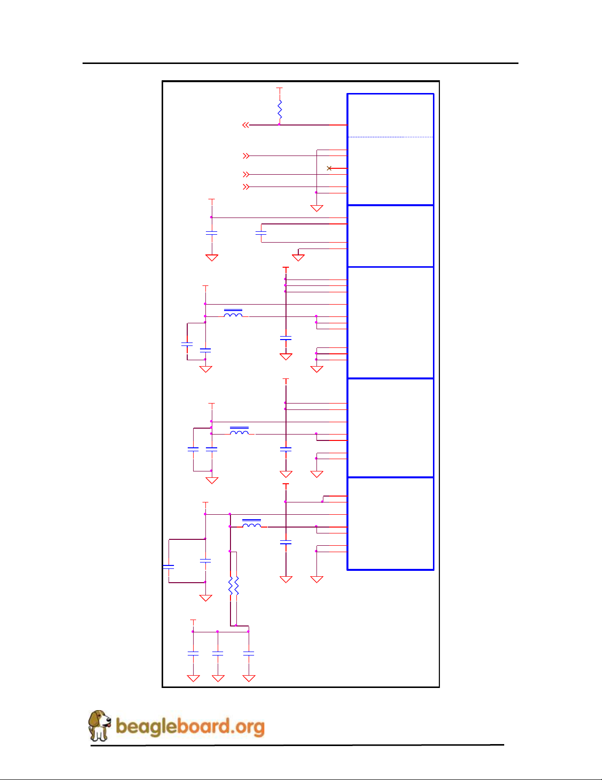
REF: BB_SRM_xM
BeagleBoard-xM System
Reference Manual
Revision C2
C1054.7uF, 6.3V,0603
VDD2
CP.C APM
I2C4_SD A4
VIO_1V8
C106
2.2uF, 6.3V
T2_VDD1.L
I2C4_SC L4
VBAT
R1
10K
CP.C APP
C112
10uF,C ER,0805,6.3V
nSLEEP4
L4
1uH,2A, LM3015
1 2
L6
1uH,2A, LM3015
1 2
T2_VDD2.L
L5
1uH,LM3010
1 2
C111
10uF,C ER,0805,6.3V
T2_VIO.L
C119
10uF,C ER,0805,6.3V
C139
0.1uF, 10V
C118
10uF,C ER,0805,6.3V
C132
10uF,C ER,0805,6.3V
R670,0603
C136
10uF,C ER,0805,6.3V
C140
10uF,C ER,0805,6.3V
C110
0.1uF, 10V
C117
0.1uF, 10V
REGEN8
MEM_1V8
C189
10uF,C ER,0805,6.3V
R660,0603
VBAT
VDD1
VDD2
VIO
USB CP
Power control
VBAT
IO_1P8
U7B TPS65950
VIO.GN D
T3
VIO.GN D
R2
VIO.L
T4
VIO.L
R3
VIO.OU T
N3
VIO.I N
R4
VIO.I N
P3
VDD2. GND
R15
VDD2. GND
T14
VDD2. L
R14
VDD2. L
T13
VDD2. FB
N13
VDD2. IN
P14
VDD2. IN
R13
VDD1. GND
C15
VDD1. GND
B15
VDD1. GND
C16
VDD1. OUT
E13
VDD1. L
C14
VDD1. L
D15
VDD1. L
D16
VDD1. IN
E14
VDD1. IN
D14
VDD1. IN
E15
CP.C APP
T7
CP.C APM
T6
CP.I N
R7
CP.GN D
R6
N.C ./I2C. SR. SDA
C4
VMODE2(VDD2)/ I2C.SR. SCL
D6
N.C.
B14
nSLEEP1
P7
nSLEEP2
G9
VMODE1(VDD1)
F8
REGEN
A10
VBAT
VDD1
VBAT
VBAT
C138
0.1uF, 10V
Figure 25. Main Power Rails
Page 57 of 163
Page 58

REF: BB_SRM_xM
BeagleBoard-xM System
Reference Manual
Revision C2
7.7.5 Main Core Voltages Smart Reflex
VDD1 and VDD2 regulators on the TPS65950 provide SmartReflex-compliant voltage
management. The SmartReflex controller in the processor interfaces with the TPS65950
counterpart through the use of a dedicated I2C bus. The processor computes the required
voltage and informs the TPS65950 using the SmartReflex I2C interface.
SmartReflex control of the VDD1 and VDD2 regulators can be enabled by setting the
SMARTREFLEX_ENABLE bit (DCDC_GLOBAL_CFG[3]) to 1. To perform VDD1
voltage control through the SmartReflex interface, the TPS65950 provides the
VDD1_SR_CONTROL register. The MODE field of the VDD1_SR_CONTROL register
can be set to 0 to put VDD1 in an ACTIVE state; setting the field to 1 moves VDD1 to a
SLEEP state. VDD1 output voltage can be programmed by setting the VSEL field of the
VDD1_SR_ CONTROL register. The VDD1 output voltage is given by VSEL*12.5 mV
+ 600 mV.
7.7.6 VDD1
The VDD1 rail is supplied by the VDD1 regulator of the TPS65950. The VDD1
regulator is a 1.1A stepdown power converter with configurable output voltage between
0.6 V and 1.45 V in steps of 12.5 mV. This regulator is used to power the processor core.
The processor can request the TPS65950 to scale the VDD1 output voltage to reduce
power consumption. The default output voltage at power-up depends on the boot mode
settings, which in the case of the BeagleBoard is 1.2V. The output voltage of the VDD1
regulator can be scaled by software or hardware by setting the ENABLE_VMODE bit
(VDD1_VMODE_CFG[0]). In each of these modes, the output voltage ramp can be
single-step or multiple-step, depending on the value of the STEP_REG field of the
VDD1_STEP[4:0] register. The VOCORE_1V3 rail should be set to 1.3V after boot up.
Apart from these modes, the VDD1 output voltage can also be controlled by the
processor through the SmartReflex I2C interface between the DM3730 and the
TPS65950. The default voltage scaling method selected at reset is a software-controlled
mode. Regardless of the mode used, VDD1 can be configured to the same output voltage
in sleep mode as in active mode by programming the DCDC_SLP bit of the
VDD1_VMODE_CFG[2] register to 0. When the DCDC_SLP bit is 1, the sleep mode
output voltage of VDD1 equals the floor voltage that corresponds to the VFLOOR field
(VDD1_VFLOOR[6:0]).
7.7.7 VDD2
The VDD2 voltage rail is generated by the TPS65950 using the VDD2 regulator. The
VDD2 regulator is a stepdown converter with a configurable output voltage of between
Page 58 of 163
Page 59

REF: BB_SRM_xM
BeagleBoard-xM System
Reference Manual
Revision C2
0.6 V and 1.45 V and is used to power the processor core. VDD2 differs from VDD1 in
its current load capabilities with an output current rating of 600 mA in active mode.
The VDD2 provides different voltage regulation schemes. When VDD2 is controlled by
the VMODE2 signal or with the SmartReflex interface, the range of output voltage is 0.6
V to 1.45 V. The use of the VMODE2 signal and the VDD2_VMODE_CFG,
VDD2_STEP, VDD2_FLOOR, and VDD2_ROOF registers is similar to the use of the
corresponding signals and registers for VDD1. VDD2 shares the same SmartReflex I2C
bus to provide voltage regulation. The VDD2_SR_CONTROL register is provided for
controlling the VDD2 output voltage in SmartReflex mode.
When the VDD2 is used in software-control mode, the VSEL (VDD2_
DEDICATED[4:0]) field can be programmed to provide output voltages of between 0.6
V and 1.45 V. The output voltage for a given value of the VSEL field is given by
VSEL*12.5 mV + 600 mV. If the VSEL field is programmed so that the output voltage
computes to more than 1.45 V, the TPS65950 sets the VDD2 output voltage to 1.5 V.
7.8 Peripheral Voltages
There are 10 additional voltages used by the system that are generated by the TPS65950.
These are:
o VDD_PLL2
o VDD_PLL1
o VDAC_1V8
o VDD_SIM
o VMMC2
o VDD_VMMC1
o CAM_2V8
o CAM_1V8
o USB_1V8
o EXP_VDD
Figure 27 shows the peripheral voltages supplied by the TPS65950.
7.8.1 VDD_PLL2
This programmable LDO is used to power the processor PLL circuitry. The VPLL2 LDO
can be configured through the I2C interface to provide output voltage levels of 1.0 V, 1.2
V, 1.3 V, or 1.8 V, based on the value of the VSEL field (VPLLI_DEDICATED[3:0]).
On the board this rail is used to power DVI output for pins DSS_DATA(0:5),
DSS_DATA(10:15) and DSS_DATA(22:23). The VPLL2 must be set to 1.8V for proper
operation of the DVI-D interface.
Page 59 of 163
Page 60
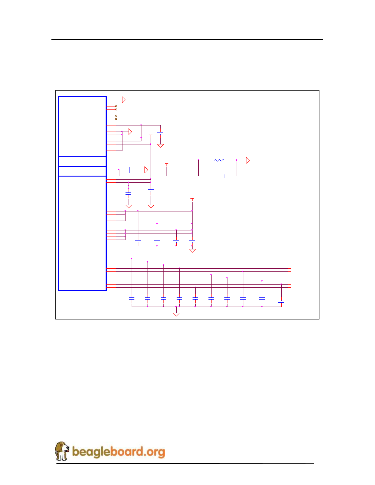
REF: BB_SRM_xM
BeagleBoard-xM System
Reference Manual
Revision C2
BCI
Backup battery
IO Level
IO_1P8
U7B TPS65950
VBAT
R5
BKBAT
M14
ICTLAC2
P2
ICTLAC1
N7
ICTLUSB2
P1
ICTLUSB1
P6
BCIAU TO
N1
VPRECH
N2
PCHGU SB
N6
PCHGAC
N4
VBATS
P4
VAC
N5
VCCS
P5
VPLL2
J15
VPLL1
H14
VDAC. OUT
L2
VSIM
K2
VMMC2.OUT
A4
VMMC1.OUT
C2
VAUX4.OUT
B3
VAUX3.OUT
G16
VAUX2.OUT
M3
VAUX1.OUT
M2
VBAT.RIGH T
D11
VBAT.RIGH T
D12
VDAC. IN
K1
VMMC2.IN
A3
VMMC1.IN
C1
VAUX4.IN
B2
VPLLA3R
H15
VAUX12S
L1
VBAT.LEFT
D10
VBAT.LEFT
D9
VBAT.USB
R9
IO.1P8
C8
VINT
K15
R65
0,0603
VDD_SI M
BKBAT
T2_VPRECH
BT1
BAT_LI_RTC
C122
2.2uF, 6.3V
VDAC_1V8
C104
0.1uF, 10V
EXP_VDD
VIO_1V8
VDD_PLL2
VDD_PLL1
VIO_1P8
C108
1uF,10V
(1.85V-3V)
USB_1V8
C109
1uF,10V
CAM_1V8
VMMC2
C116
1uF,10V
CAM_2V8
C115
1uF,10V
C107 0. 1uF,10V
C127
1uF,10V
C114
1uF,10V
C113
1uF,10V
C124
1uF,10V
C123
1uF,10V
VBAT
C125
1uF,10V
VBAT
C120
1uF,10V
C126
1uF,10V
C121
1uF,10V
VDD_MMC1
C213
1uF,10V
C128
10uF,C ER,0805,6.3V
7.8.2 VDD_PLL1
The VPLL1 programmable LDO regulator is low-noise, linear regulator used for the
processor PLL supply. The VDD_PLL1 rail is initialized to 1.8V.
7.8.3 VDAC_1V8
The VDAC programmable LDO regulator is a high-PSRR, low-noise, linear regulator
that powers the PROCESSOR dual-video DAC. It is controllable with registers via I2C
and can be powered down if needed. The VDAC LDO can be configured to provide
1.2V, 1.3 V, or 1.8 V in on power mode, based on the value of the VSEL field
(VDAC_DEDICATED[3:0]). The VDAC_1V8 rail should be set to 1.8V for the
BeagleBoard.
Figure 26. Peripheral Voltages
Page 60 of 163
Page 61

REF: BB_SRM_xM
BeagleBoard-xM System
Reference Manual
Revision C2
7.8.4 VDD_SIM
This voltage regulator is a programmable, low dropout, linear voltage regulator supplying
the bottom 4 bits of the 8 bit SD/MMC card slot. The VSEL field
(VSIM_DEDICATED[3:0]) can be programmed to provide output voltage of 1.0 V, 1.2
V, 1.3 V, 1.8 V, 2.8 V, or 3.0 V and can deliver up to 50mA. The default output voltage
of this LDO as directed by the TPS65950 boot pins is 1.8V.
7.8.5 VMMC2
The VMMC2 rail uses the VMMC2.OUT rail from the TP65950. VMMC2 is adjustable
from 1.85 to 3.15V and can deliver up to 100mA of current. VMMC2 is provided as an
auxiliary voltage rail on P17, the Auxiliary Access Header. The proper setting of this rail
is determined by the application and the HW supplied that connects to P17.
7.8.6 VDD_VMMC1
The VMMC1 LDO regulator is a programmable linear voltage converter that powers the
MMC1 slot and includes a discharge resistor and overcurrent protection (short-circuit).
This LDO regulator can also be turned off automatically when the MMC card extraction
is detected. The VMMC1 LDO is powered from the main VBAT rail. The VMMC1 rail
defaults to 3.0V as directed by the TPS65950 boot pins and will deliver up to 220mA. It
can be set to 3.0V in the event 3V cards are being used.
7.8.7 CAM_2V8
This rail powers the optional camera module and uses the VAUX4.OUT rail from the
TPS65950. VAUX4 is adjustable from .7 to 2.8V and can deliver up to 200mA of power.
This railed should be set to 1.8V for proper operation of the camera module. See the
camera module section for more information.
7.8.8 CAM_1V8
This rail powers the optional camera module and uses the VAUX3.OUT rail from the
TPS65950. VAUX4 is adjustable from 1.5 to 2.8V and can deliver up to 100mA of
power. This railed should be set to 1.8V for proper operation of the camera module. See
the camera module section for more information.
7.8.9 USB_1V8
The VAUX2 LDO regulator is a programmable linear voltage converter that powers the
1.8V I/O rail of the USB PHY and includes a discharge resistor and overcurrent
protection (short-circuit). The VAUX2 LDO is powered from the main VBAT rail. The
VAUX2 rail defaults to off as directed by the TPS65950 boot pins and will deliver up to
100mA. The voltage rail is labeled VDD_EHCI on the schematic.
Page 61 of 163
Page 62

REF: BB_SRM_xM
BeagleBoard-xM System
Reference Manual
Revision C2
7.8.10 EXP_VDD
The EXP_VDD rail uses the VAUX1.OUT rail from the TP65950. EXP_VDD is
adjustable from 2.5 to 3.0V and can deliver up to 200mA of current. EXP_VDD is
provided as an auxiliary voltage rail on P13, the LCD Expansion Header. The proper
setting of this rail is determined by the application and the HW supplied that connects to
P13.
7.9 Other Signals
This section describes other signals in the design that have not been categorized.
7.9.1 Boot Configuration
The boot configuration pins on the TPS65950 determine the power sequence of the
device. In order to support the processor on the board with the correct power
configuration, the boot pin configuration is fixed at:
o BOOT0 tied to VBAT
o BOOT1 tied to Ground.
7.9.2 RTC Backup Battery
An optional battery to backup for the Real Time Clock that is in the TPS65950 is
provided for in the design. The board does not come equipped with the battery. The
battery can be purchased from DigiKey or other component suppliers. When the battery
is not installed, R65 must be installed. You must make sure that prior to installing the
battery that R65 is removed.
Refer to section 9.11 for information on the battery selection and installation.
Page 62 of 163
Page 63
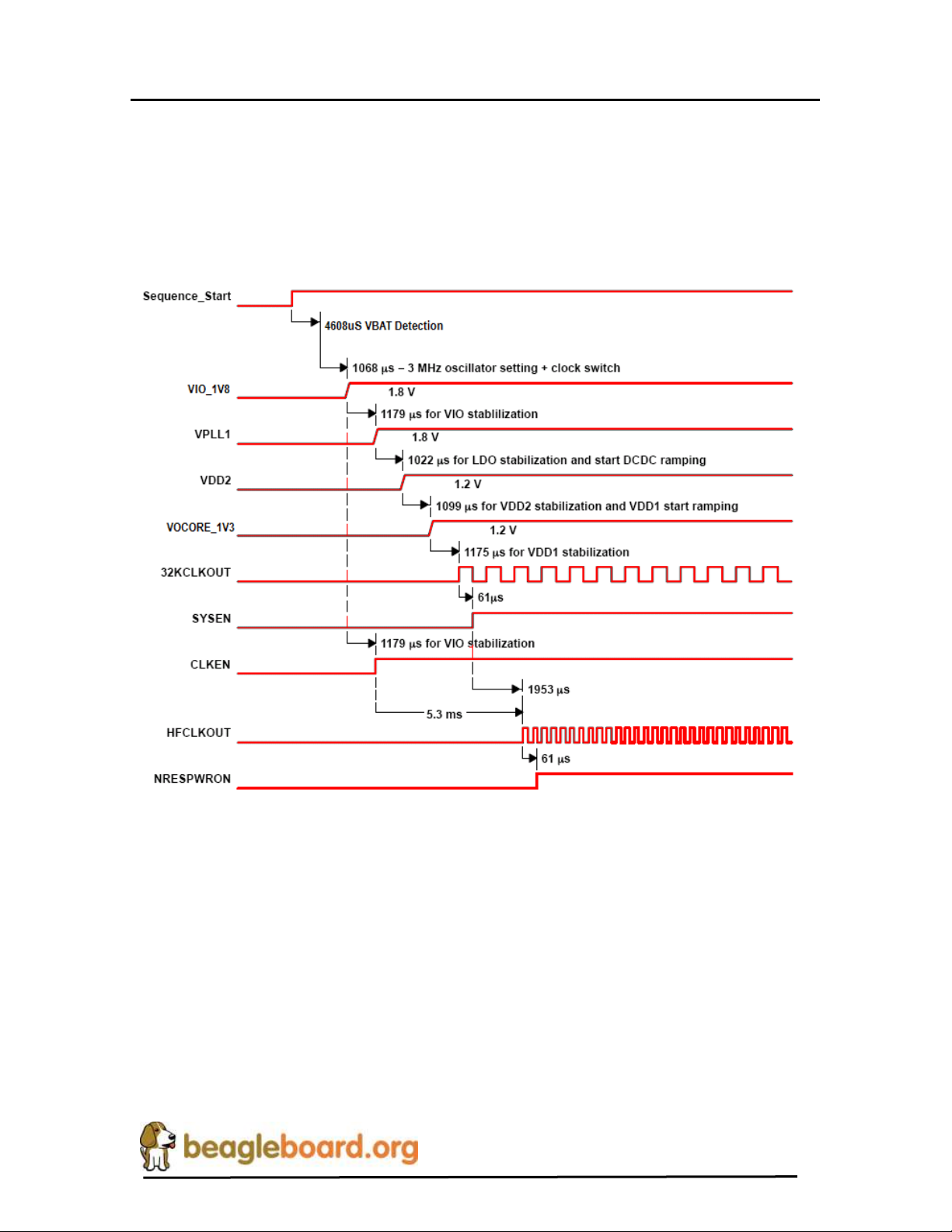
REF: BB_SRM_xM
BeagleBoard-xM System
Reference Manual
Revision C2
7.9.3 Power Sequencing
Based on the boot configuration pins, the TPS65950 knows the type of OMAP processor
that it needs to support, in this case the processor. The voltages are ramped in a sequence
that is compatible with the processor. Figure 27 is the sequence in which the power rails,
clocks, and reset signal come up.
7.9.4 Reset Signals
The BeagleBoard uses three distinct reset circuits:
o Warm Reset
o Cold Reset
o User Reset
Figure 28 shows the connections for the Reset interfaces.
Figure 27. Power Sequencing
Page 63 of 163
Page 64
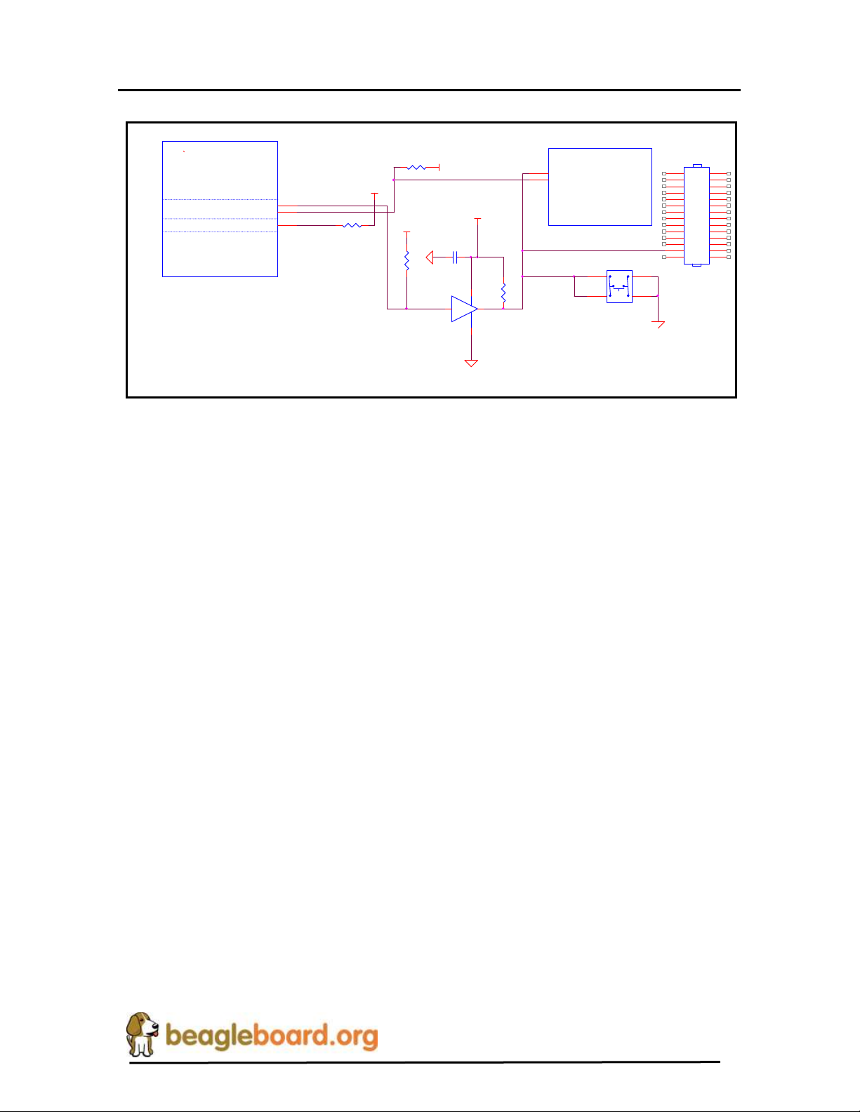
REF: BB_SRM_xM
BeagleBoard-xM System
Reference Manual
Revision C2
P9 2 4 6 8
10
12
14
16
18
20
22
24
26
28 1 3 5 7 9 11
13
15
17
19
21
23
25
27
R61
4.7K
VIO_1V8
U5A
SN74LVC2G07DCKR
1
2
5
6
VBAT
IO_1P8
T
P
S
6
5
9
5
0
U7A
B13
A13
A11
nRESWARM
nRESPWRON
PWRON
nRESPWRON
VIO_1V8
R42
10K
C12
0.1uF
VBAT
PWRON
R59
4.7K
S2
B3F-1000
1
3
2
4
R53
DNI
nRESWARM
VIO_1V8
PROCESSOR
U4B
DM3730
AH25
AF24
SYS_nRESPWRON
SYS_nRESWARM/GPIO_30
nRESET
The warm reset is generated by the processor on power up. The nRESWARM signal is a
bidirectional reset. When an internal reset occurs, nRESWARM goes low and resets all
the peripherals and the TPS65950. The TPS65950 can be configured to perform a warm
reset of the device to bring it into a known defined state by detecting a request for a warm
reset on the NRESWARM pin. The minimum duration of the pulse on the nRESWARM
pin should be two 32-kHz clock cycles. The nRESWARM output is open-drain;
consequently, an external pullup resistor is required. There is no way for the user to
generate a warm reset on the BeagleBoard.
On power up as shown in Figure 27, the TPS65950 generates nRESPWRON, power on
reset. The signal from the TPS65950 is an output only and is not an open drain signal.
By running the signal through a buffer, SN74LVC2G07, the signal becomes open drain,
which requires a pullup on the signal. This will allow the nRESPWRON signal to be
pulled low, by pressing the reset switch S2, to force a reset to the PROCESSOR
processor and to any device on the expansion card that require a reset.
It also allows for the reset signal to be pulled low or held low for an extended time by
circuitry on the expansion card if needed.
The USER RESET button can be used to request a Warm Reset from the processor. After
initialization, this pin becomes an input to the processor. By pushing the Reset button, an
interrupt is generated into the processor. The software that is run as a result of this can
then do whatever housekeeping is required and then send the processor into a reset mode.
Figure 28. Reset Circuitry
7.9.4.1 Warm Reset
7.9.4.2 Cold Reset
7.9.4.3 User Reset
Page 64 of 163
Page 65
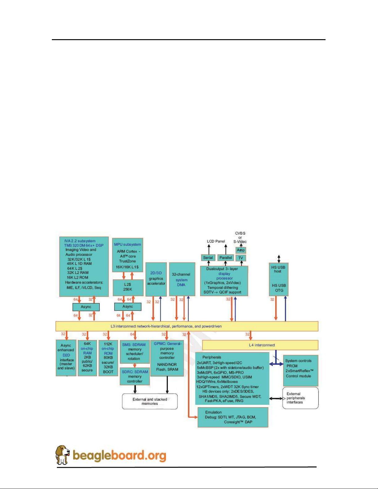
REF: BB_SRM_xM
BeagleBoard-xM System
Reference Manual
Revision C2
7.9.4.4 PWRON
You will notice another signal on the TPS65950 called PWRON. This signal is
referenced in the TPS65950 documentation. In the BeagleBoard design it is not used but
it is pulled high to insure the desired operation is maintained.
7.9.5 mSecure Signal
This signal provides for protection of the RTC registers in the TPS65950 be disabling
that function via a control signal from the processor.
For more information on the operation on the signal, please refer to the processor
Technical Reference Manual.
7.10 Processor
The heart of BeagleBoard-xM is the DM3730 processor. Figure 29 is a high level block
diagram of the processor.
Figure 29. DM37x Block Diagram
Page 65 of 163
Page 66

REF: BB_SRM_xM
BeagleBoard-xM System
Reference Manual
Revision C2
7.10.1 Overview
The DM3730 is a high-performance, multimedia application device and is integrated onto
TI's advanced 45-nm process technology. The processor architecture is configured with
different sets of features in different tier devices. Some features are not available in the
lower-tier devices. For more information, refer to the Technical Reference Manual
(TRM).The architecture is designed to provide best-in-class video, image, and graphics
processing sufficient to various applications.
The processor supports high-level operating systems (OSs), such as:
o Windows CE
o Linux
o QNX
o Symbian
o Others
This processor device includes state-of-the-art power-management techniques required
for high-performance low power products. The DM3730 supports the following functions
and interfaces on the BeagleBoard:
o Microprocessor unit (MPU) subsystem based on the ARM Cortex-A8™
microprocessor
o POP Memory interface
o 4Gb MDDR (512Mbytes)
o 24 Bit RGB Display interface (DSS)
o SD/MMC interface
o USB OTG interface
o NTSC/PAL/S-Video output
o Power management
o Serial interface
o I2C interface
o I2S Audio interface (McBSP2)
o Expansion McBSP1
o JTAG debugging interface
7.10.2 SDRAM Bus
The SDRAM bus is not accessible on the BeagleBoard. Its connectivity is limited to the
POP memory access on the top of the processor and therefore is only accessible by the
SDRAM memory. The base address for the DDR SDRAM in the POP device is 0x8000
0000.
If you look at the –xM schematic, you will notice on page 3 there are a lot of signals
labeled NA0…65. These pins are located on the bottom of the processor. In the Rev
Page 66 of 163
Page 67
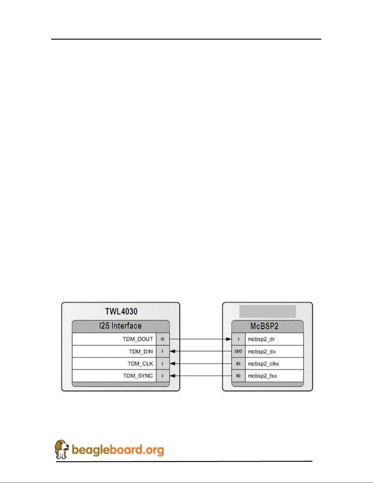
REF: BB_SRM_xM
BeagleBoard-xM System
Reference Manual
Revision C2
Processor
BeagleBoard processor, these pins provided access to the SDRAM bus. However, in the
case of the processor on the BeagleBoard–xM, these there are no signals on these pins.
7.10.3 GPMC Bus
The GPMC bus is not accessible on the BeagleBoard. Its connectivity is limited to the
POP memory access on the top of the processor and therefore is only accessible by the
NAND memory.
The memory on the GPMC bus is NAND and therefore will support the classical NAND
interface. The address of the memory space is programmable.
7.10.4 DSS Bus
The display subsystem provides the logic to display a video frame from the memory
frame buffer in SDRAM onto a liquid-crystal display (LCD) display via the DVI-D
interface or to a standalone LCD panel via the LCD interface connectors. The logic levels
of the LCD expansion connectors are 1.8V so it will require buffering of the signals to
drive most LCD panels. The DSS is configured to a maximum of 24 bits, but can be used
in lower bit modes if needed.
7.10.5 McBSP2
The multi-channel buffered serial port (McBSP) McBSP2 provides a full-duplex direct
serial interface between the processor and the audio CODEC in the TPS65950 using the
I2S format. Only four signals are supported on the McBSP2 port. Figure 30 is a
depiction of McBSP2.
7.10.6 McBSP1
Figure 30. McBSP2 Interface
Page 67 of 163
Page 68
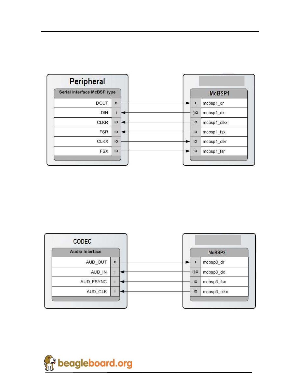
REF: BB_SRM_xM
BeagleBoard-xM System
Reference Manual
Revision C2
Processor
Processor
McBSP1 provides a full-duplex direct serial interface between the processor and the
expansion interface. There are 6 signals supported on McBSP1, unlike the 4 signals on
the other ports. Figure 31 is a diagram of McBSP1.
Figure 31. McBSP1 Interface
7.10.7 McBSP3
McBSP3 provides a full-duplex direct serial interface between the processor and the
expansion interface. Figure 32 is a diagram of McBSP3.
Figure 32. McBSP3 Interface
7.10.8 Pin Muxing
Page 68 of 163
Page 69
REF: BB_SRM_xM
BeagleBoard-xM System
Reference Manual
Revision C2
Signal
Mode
DSS
Default
MMC1
Default
MMC2
User
UART3
Default
GPMC
Default
UART1
Default
I2C1
Default
I2C2
Default
I2C3
Default
I2C4
Default
JTAG
FIXED
TV_OUT
Default
SYS_nRESPWRON
Default
SYS_nRESWARM
Default
SYS_nIRQ
Default
SYS_OFF
Default
SYS_CLKOUT
Default
SYS_CLKOUT2
Default
SYS_CLKREQ
Default
SYS_XTALIN
FIXED
GPIO_149
4
GPIO_150
4
McBSP1
Default
McBSP2
User
McBSP3
Default
GPIO_171
4
GPIO_172
4
On the processor, the majority of pins have multiple configurations that the pin can be set
to. In essence, the pin can become different signals depending on how they are set in the
software. In order for the BeagleBoard to operate, the pins used must be set to the correct
signal. In some cases, the default signal is the correct signal. Each pin can have a
maximum of 8 options on the pin. This is called the pin mode and is indicated by a three
bit value (0:3). In the case of the signals going to the expansion connector, the settings
required for those pins depends on how they are to be used. For an explanation of the
options, please refer to the Expansion Header section. Each pin can be set to a different
mode independent of the other pins on the connector.
Table 4 is a list of all of the signals used on the processor for the BeagleBoard and the
required mode setting for each pin. Where the default setting is needed, it will be
indicated. The USER notation under mode indicates that this is an expansion signal and
can be set at the discretion of the user. A FIXED indicates that there is only one function
for that signal and that it cannot be changed,
Table 4. Processor Pin Muxing Settings
Page 69 of 163
Page 70
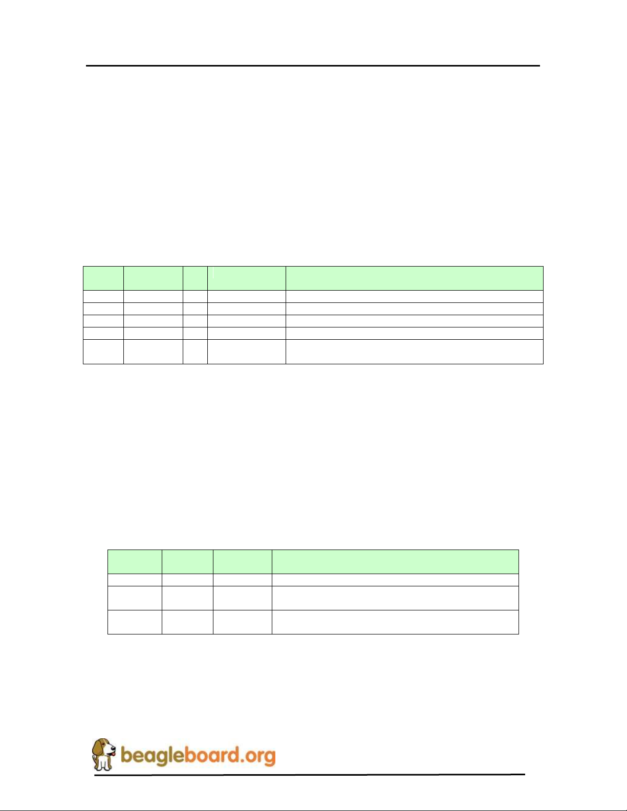
REF: BB_SRM_xM
BeagleBoard-xM System
Reference Manual
Revision C2
OMAP
PIN
INT/GPIO
I/O
Signal
USAGE
AA9
GPIO_150
O
LED_GPIO150
Controls User LED0
W8
GPIO_149
O
LED_GPIO149
Controls User LED1
AG9
GPIO_23
I
MMC1_WP
SD/MMC card slot Write protect
J25
GPIO_170
O
DVI_PUP
Controls the DVI-D interface. A Hi = DVI-D enabled.
AE21
GPIO_4
I
SYSBOOT_5
Used to put the device in the boot mode or as the USER
BUTTON input.
TPS65950
Pin
Processor
PIN
INT/GPIO
USAGE
AF26
SYS_nIRQ
Interrupt from the TPS65950
AH8
GPIO_29
SD Write protect lead. Can be polled or set to an
interrupt.
P12
GPIO0
MMC1 card detect input. Goes to the processor over the
SYS_nIRQ pin.
7.10.9 GPIO Mapping
There are a number of GPIO pins from the processor that are used on the BeagleBoard
design. Table 5 shows which of these GPIO pins are used in the design and whether they
are inputs or outputs. While GPIO pins can be used as interrupts, the table only covers the
GPIO pin mode. If it is an interrupt, then it is covered in the interrupt section.
Table 5. Processor GPIO Pins
Other signals, such as those that connect to the expansion connector, may also be set as a
GPIO pin. For information on those, refer to the Expansion Connector section.
7.10.10 Interrupt Mapping
There are a small number of pins on the processor that act as interrupts. Some of these
interrupts are connected to the TPS65950 and their status is reflected through the main
TPS65950 interrupt. Table 6 lists the interrupts.
Table 6. Processor Interrupt Pins
Page 70 of 163
Page 71
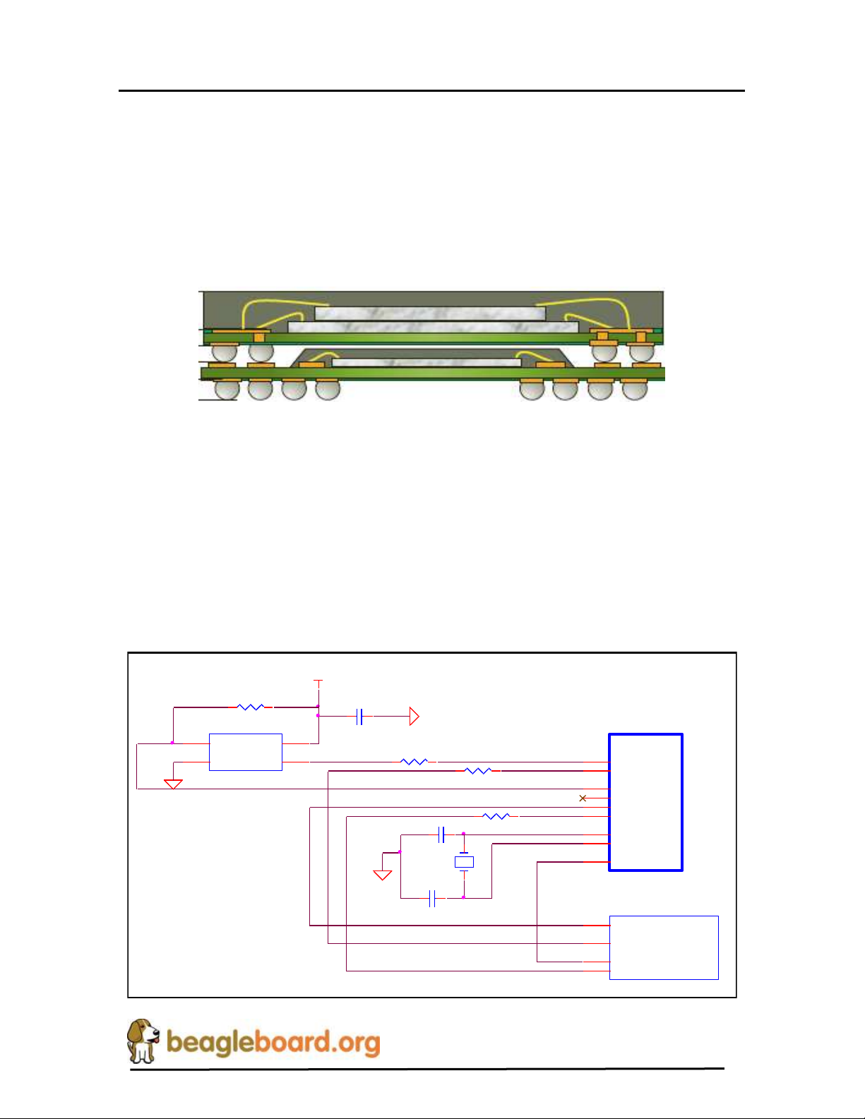
REF: BB_SRM_xM
BeagleBoard-xM System
Reference Manual
Revision C2
U4BOMAP3730_ES1.0
SYS_XTALIN
AE17
SYS_32K
AE25
SYS_C LKREQ/GPI O_1
AF25
McBSP_CLKS
T21
U7A TPS65950
32KCLKOUT
N10
32KXIN
P16
32KXOUT
P15
HFC LKIN
A14
HFC LKOUT
R12
CLKEN
C6
CLKEN2
D7
CLKREQ
G10
CLK256FS
D13
CLK256FS
HFC LK_26MHz
OSC_EN
R51 33
R47 33
HFC LKOUT
T2_XOUT
C102 22PF
T2_XIN
C103 22PF
Y3
32KHz Cry stal
1 2
C85 0. 1uF,10V
VIO_1V8
Y1
OSC_26MHZ_EAE
COM/CASE
2
NC1+VCC
4
OUT
3
26MHZ
R56 33
R55 4.7K
OSC_EN
Processor
7.11 POP Memory Device
The processor uses what is called POP (Package-on-Package) memory. The memory is a
MCP (Multi Chip Package) that contains a dual Mobile DDR SDRAM stack. Figure 33
shows the POP Memory concept.
Figure 33. POP Memory
The Memory device mounts on top of the processor. The configuration used on the board
is a 200MHz 4Gb MDDR SDRAM device from Micron.
7.12 System Clocks
There are three main clocks needed for the operation of the board, 32KHz, 26MHz and
McBSP_CLKS. Figure 34 shows the components that make up the System Clocks.
There are additional clocks needed elsewhere in the system, such as USB HUB, but those
are discussed in separate sections.
Page 71 of 163
Page 72

REF: BB_SRM_xM
BeagleBoard-xM System
Reference Manual
Revision C2
Figure 34. System Clocks
7.12.1 32KHz Clock
The 32KHz clock is needed for the TPS65950 and the processor and is provided by the
TPS65950 via the external 32KHz crystal, Y2. The TPS65950 has a separate output from
the crystal to drive the processor that buffers the resulting 32-kHz signal and provides it
as 32KCLKOUT, which is provided to the processor on ball AE25. The default mode of
the 32KCLKOUT signal is active, but it can be disabled if desired under SW control.
The 32.768-kHz clock drives the RTC embedded in the TPS65950. The RTC is not
enabled by default; the host processor must set the correct date and time to enable the
RTC.
7.12.2 26MHz Clock
This section describes the 26MHz clock section of the BeagleBoard.
7.12.2.1 26MHz Source
The BeagleBoard is designed to support two suppliers of the 26MHz oscillator. The
26MHz clock is provided by an onboard oscillator, Y1. The TPS65950 receives the
external HFCLKIN signal on ball A14 and uses it to synchronize or generate the clocks
required to operate the TPS65950 subsystems. The TPS65950 must have this clock in
order to function to the point where it can power up the BeagleBoard. This is the reason
the 26MHz clock is routed through the TPS65950.
7.12.2.2 TPS65950 Setup
When the TPS65950 enters an active state, the Processor must immediately indicate the
HFCLKIN frequency (26 MHz) by setting the HFCLK_FREQ bit field (bits [1:0]) in the
CFG_BOOT register of the TPS65950. HFCLK_FREQ has a default of being not
programmed, and in that condition, the USB subsection does not work. The three DCDC
switching supplies (VIO, VDD1, and VDD2) operate from their free-running 3-MHz
(RC) oscillators, and the PWR registers are accessed at a default 1.5-M byte.
HFCLK_FREQ must be set by the processor during the initial power-up sequence. On the
BeagleBoard, this is done by the internal boot ROM on startup.
7.12.2.3 Processor 26MHz
The 26MHz clock for the processor is provided by the TPS65950 on ball R12 through
R38, a 33 ohm resistor is providing to minimize any reflections on the clock line. The
clock signal enters via ball AE17 on the PROCESSOR.
Page 72 of 163
Page 73

REF: BB_SRM_xM
BeagleBoard-xM System
Reference Manual
Revision C2
NOTE: In order to use the OTG in the Host mode, the
BeagleBoard must be powered from the DC supply.
7.12.3 McBSP_CLKS
An additional clock is also provided by the TPS65950 called McBSP_CLKS. This clock
is provided to the PROCESSOR in order to insure synchronization of the I2S interface
between the processor and the TPS65950.
7.13 USB OTG Port
The BeagleBoard has a USB OTG (On-the-Go) port. It can be used as an OTG port,
Client port, or Host port. The main use is as a client port, as that is the mode that will
supply the power needed to power the BeagleBoard. With the addition of the USB Host
ports, the need to use three OTG port as a Host, is not really needed.
7.13.1 USB OTG Overview
USB OTG is a supplement to the USB 2.0 specification. The standard USB uses a
master/slave architecture, a USB host acting as a master and a USB peripheral acting as a
slave. Only the USB host can schedule the configuration and data transfers over the link.
The USB peripherals cannot initiate data transfers, they only respond to instructions
given by a host.
USB OTG works differently in that gadgets don't need to be pure peripherals because
they can sometimes act as hosts. An example might be connecting a USB keyboard or
printer to BeagleBoard or a USB printer that knows how to grab documents from certain
peripherals and print them. The USB OTG compatible devices are able to initiate the
session, control the connection and exchange Host/Peripheral roles between each other.
The USB OTG supplement does not prevent the use of a hub, but it describes role
swapping only in the case of a one-to-one connection where two OTG devices are
directly connected. If a standard hub is used, the supplement notes that using it will lead
to losing USB OTG role-swap capabilities making one device as the Default-Host and the
other as the Default-Peripheral until the hub is disconnected.
The combination of the processor and the TPS65950 allows the BeagleBoard to work as
an OTG device if desired. The primary mode of operation however, is intended to be a
client mode in order to pull power from the USB host which is typically a PC. As the Rev
B does not have a Host USB port, this port will be used as a Host port in many
applications.
Page 73 of 163
Page 74
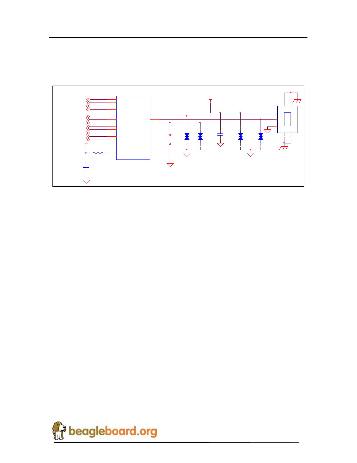
REF: BB_SRM_xM
BeagleBoard-xM System
Reference Manual
Revision C2
P1
mini U SB-AB
D-
2
D+
3
VB
1
ID
4
G27G3
6
G1
5
G58G4
9
+
J1
JMP
1 2
U7A TPS65950
VBUS
R8
DP
T10
DN
T11
ID
R11
UCLK
L15
STP
L14
DIR
L13
NXT
M13
DATA0
K14
DATA1
K13
DATA2
J14
DATA3
J13
DATA7
F13
DATA6
F14
DATA4
G14
DATA5
G13
USB_CLIENT /
OTG PORT
D1
PGB0010603MR
D2
PGB0010603MR
D3
PGB0010603MRD4PGB0010603MR
VBUS_5V0
USB0HS_D AT24
USB0HS_C LK4
USB0HS_D AT14
USB0HS_D AT54
USB0HS_D AT04
USB0HS_D AT64
USB0HS_D IR4
USB0HS_D AT44
USB0HS_STP4
USB0HS_D AT74
USB0HS_N XT4
USB0HS_D AT34
R57 0,0603
VBUS_5V0
C86
4.7uF, 6.3V,0603
C3
0.1uF, 10V
7.13.2 USB OTG Design
Figure 34 is the design of the USB OTG port on the BeagleBoard.
Figure 35. USB OTG Design
7.13.3 OTG ULPI Interface
ULPI is an interface standard for high-speed USB 2.0 systems. It defines an interface
between USB link controller (processor) and the TPS65950 that drives the actual bus.
ULPI stands for UTMI+ low pin interface and is designed specifically to reduce the pin
count of discrete high-speed USB PHYs. Pin count reductions minimize the cost and
footprint of the PHY chip on the PCB and reduce the number of pins dedicated to USB
for the link controller.
.
Unlike full- and low-speed USB systems, which utilize serial interfaces, high-speed
requires a parallel interface between the controller and PHY in order to run the bus at
480Mbps. This leads to a corresponding increase in complexity and pin count. The ULPI
used on the BeagleBoard keeps this down to only 12 signals because it combines just
three control signals, plus clock, with an 8-bit bi-directional data bus. This bus is also
used for the USB packet transmission and for accessing register data in the ULPI PHY.
7.13.3.1 Processor Interface
The controller for the ULPI interface is the Processor. It provides all of the required
signals to drive the interface. Table 7 describes the signals from the processor that are
used for the USB OTG interface.
Page 74 of 163
Page 75
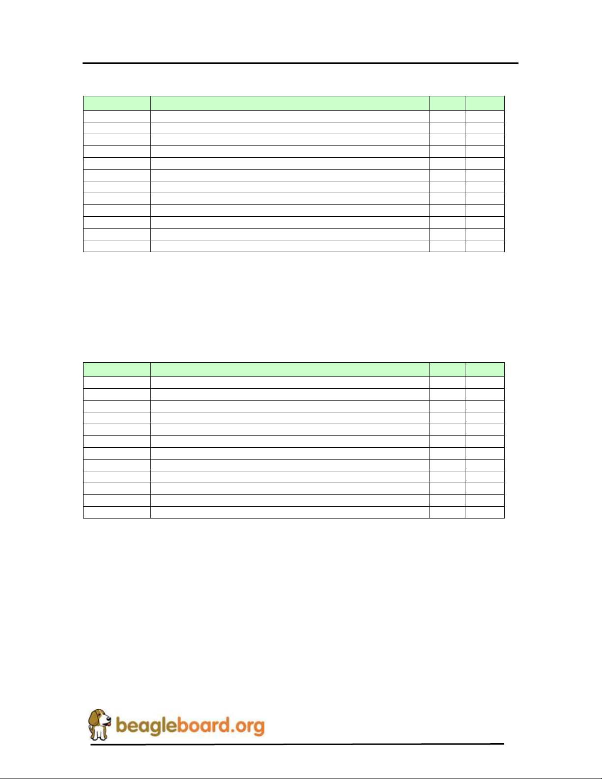
REF: BB_SRM_xM
BeagleBoard-xM System
Reference Manual
Revision C2
Signal
Description
Type
Ball
hsusb0_clk
Dedicated for external transceiver 60-MHz clock input from PHY
I
T28
hsusb0_stp
Dedicated for external transceiver Stop signal
O
T25
hsusb0_dir
Dedicated for external transceiver Data direction control from PHY
I
R28
hsusb0_nxt
Dedicated for external transceiver Next signal from PHY
I
T26
hsusb0_data0
Transceiver Bidirectional data bus
I/O
T27
hsusb0_data1
Transceiver Bidirectional data bus
I/O
U28
hsusb0_data2
Transceiver Bidirectional data bus
I/O
U27
hsusb0_data3
Transceiver Bidirectional data bus
I/O
U26
hsusb0_data4
Transceiver Bidirectional data bus
I/O
U25
hsusb0_data5
Transceiver Bidirectional data bus
I/O
V28
hsusb0_data6
Transceiver Bidirectional data bus
I/O
V27
hsusb0_data7
Transceiver Bidirectional data bus
I/O
V26
Signal
Description
Type
Ball
UCLK
High speed USB clock
I/O
L15
STP
High speed USB stop
I
L14
DIR
High speed USB dir
O
L13
NXT
High speed USB direction
O
M1
DATA0
High speed USB Data bit 0
I/O
K14
DATA1
High speed USB Data bit 0
I/O
K13
DATA2
High speed USB Data bit 0
I/O
J14
DATA3
High speed USB Data bit 0
I/O
J13
DATA4
High speed USB Data bit 0
I/O
G14
DATA5
High speed USB Data bit 0
I/O
G13
DATA6
High speed USB Data bit 0
I/O
F14
DATA7
High speed USB Data bit 0
I/O
F13
Table 7. Processor ULPI Interface
7.13.3.2 TPS65950 Interface
The TPS65950 USB interfaces to the Processor over the ULPI interface. Table 8 is a list
of the signals used on the TPS65950 for the ULPI interface.
Table 8. TPS65950 ULPI Interface
7.13.4 OTG Charge Pump
When the TPS65950 acts as an A-device, the USB charge pump is used to provide 4.8
V/100 mA to the VBUS pin. When the TPS65950 acts as a B-device, the USB charge
pump is in high impedance. If used in the OTG mode as an A-device, the BeagleBoard
will need to be powered from the DC supply. If acting as a B-device, there will not be a
voltage source on the USB OTG port to drive the BeagleBoard. Table 9 describes the
charge pump pins.
Page 75 of 163
Page 76
REF: BB_SRM_xM
BeagleBoard-xM System
Reference Manual
Revision C2
Signal
Description
Type
Ball
CP.IN
The charge pump input voltage. Connected to VBAT.
Power
R7
CP.CAPP
The charge pump flying capacitor plus.
O
L14
CP.CAPM
The charge pump flying capacitor minus.
O
T6
CP.GND
The charge pump ground.
GND
R6
Table 9. USB OTG Charge Pump Pins
The charge pump is powered by the VBAT voltage rail. The charge pump generates a
4.8-V (nominal) power supply voltage to the VBUS pin. The input voltage range is 2.7 V
to 4.5 V so the 4.2V VBAT is within this range. The charge pump operating frequency is
1 MHz. The charge pump integrates a short-circuit current limitation at 450 mA.
7.13.5 OTG USB Connector
The OTG USB interface is accessed through the miniAB USB connector. If you want to
use the OTG port as a USB Host, pin 4 of the connector must be grounded. The -xM Rev
A version of Beagle provides jumper pad, J6 that allows for a small piece of solder to be
placed on the pads to perform this function. It should be noted that with the USB Host
port on the -xM Rev A Beagle, the need to convert the OTG port to a host mode is greatly
diminished.
7.13.6 OTG USB Protection
Each lead on the USB port has ESD protection. In order for the interface to meet the USB
2.0 Specification Eye Diagram, these protection devices must be low capacitance.
7.14 Onboard USB HUB
A new feature of the –xM board is the inclusion of an onboard USB 4 port hub with an
integrated 10/100 Ethernet. This section describes the design of the HUB and the
interface to the processor. This allows for the support of LS and FS USB devices without
the need for an external USB HUB. Figure 36 is a high level block diagram of the system
design of the integrated HUB.
Page 76 of 163
Page 77
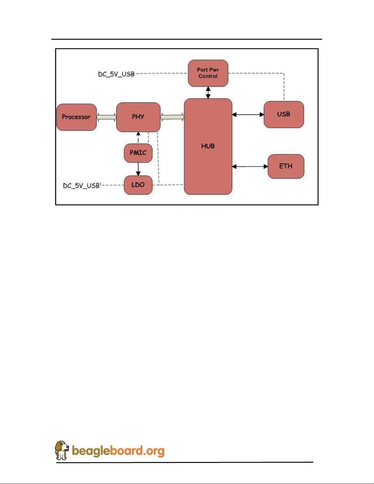
REF: BB_SRM_xM
BeagleBoard-xM System
Reference Manual
Revision C2
Figure 36. USB HUB Block Diagram
The following section covers each of the key function in the overall design.
o Power
o HS USB PHY
o HUB
o USB Port Power
o Ethernet
7.14.1 Power
The power for the HUB is provided by two sources. Figure 37 is the design of the HUB
power circuitry. The HUB_3V3 rail, the main supply rail for the HUB, is provided by
U16, a TL1963A LDO. Power for the LDO is provided by the DC_5V_USB rail from
the overvoltage protection circuit. The LDO is set to provide 3.3V and is set by R111 and
R113. This rail can be turned on or off from the processor by using the I2C bus to
communicate to the TPS65950. By default, the LDO is turned off.
The TPS65950 provides the USB_1V8 rail which is used by the USB PHY. The
processor can turn on or off this rail by communicating with the TPS65950 via the I2C
bus.
Page 77 of 163
Page 78
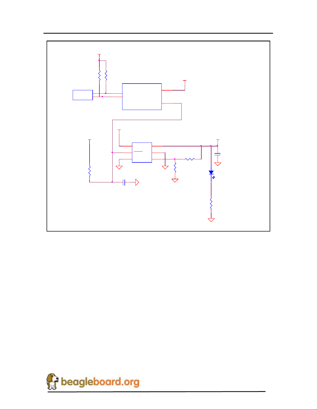
REF: BB_SRM_xM
BeagleBoard-xM System
Reference Manual
Revision C2
USB_1V8
U7A TPS65950
I2C. CNTL.SDA
D4
I2C. CNTL.SCL
D5
LEDA/VI BRA.P
F15
VAUX2.OUT
M3
VBAT HUB_3V3
DC_5V_U SB
USB ACTIVE
R136
330
USBLED_R
GRN
D14
LTST-C190GKT
R120
200K,1%,0603
C2114.7uF, 6.3V,0603
U16_FB
R111
56.2K,1%
R113
32.4K,1%
U4B
AM37xx_ES1.0
I2C1_SC L
K21
I2C1_SD A
J21
VIO_1V8
U16
TL1963A
IN
2
SHDN
1
OUT
4
ADJ
5
GND
3
GND
6
C177
4.7uF, 6.3V,0603
R1574.7K
R1594.7K
Figure 37. HUB Power Circuitry
A green LED, D14, indicates that power is applied to the HUB circuitry.
7.14.2 HS USB PHY
The configuration of the HS USB PHY is basically the same as on the Rev BeagleBoard
design. A PHY is required between the processor ULPI interface and the USB HUB.
Figure 39 shows the processor and PHY interface.
Page 78 of 163
Page 79
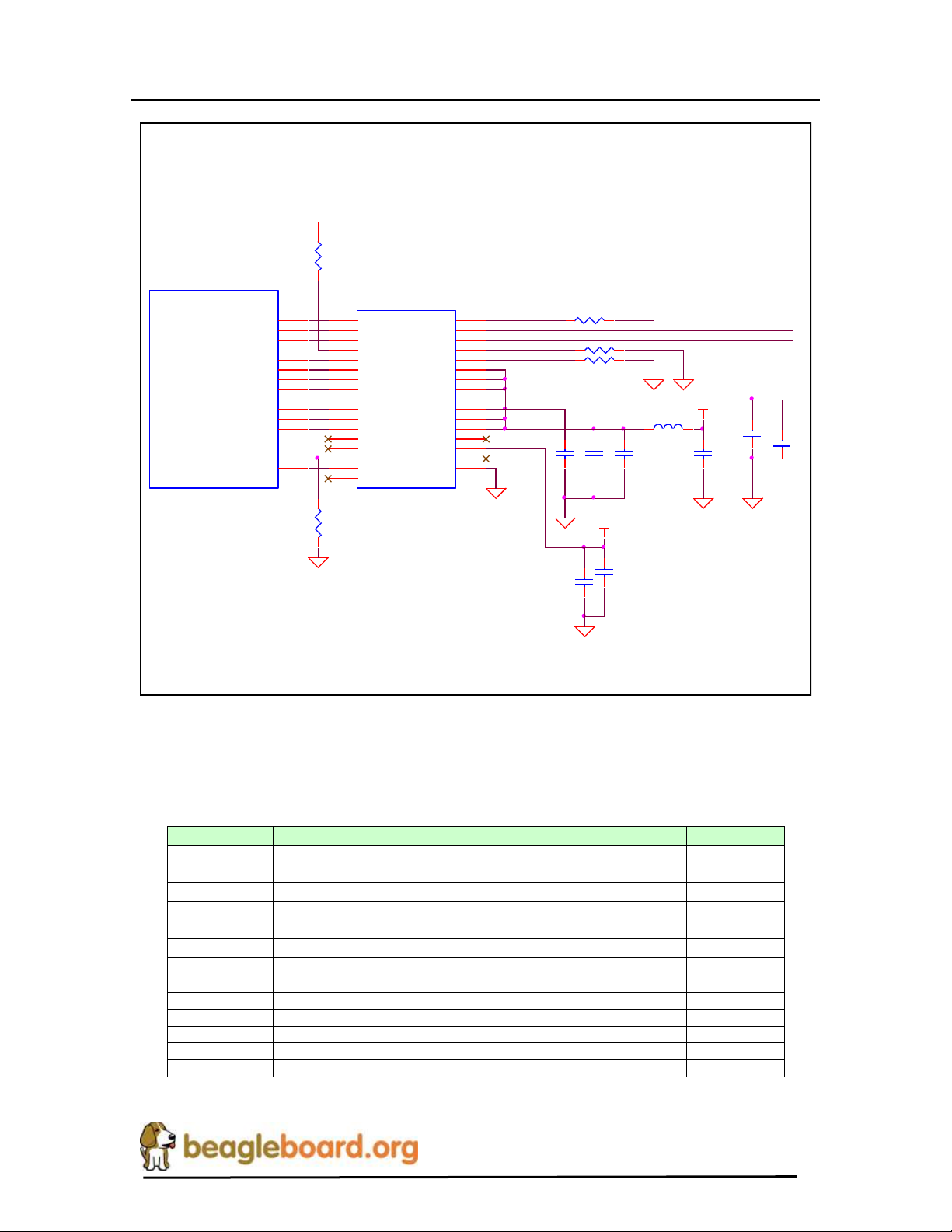
REF: BB_SRM_xM
BeagleBoard-xM System
Reference Manual
Revision C2
U4BOMAP3730_ES1.0
HSUSB2_D 7
AA3
HSUSB2_D 4
Y2
HSUSB2_D 5
Y3
HSUSB2_D 6
Y4
HSUSB2_C LK
AE7
HSUSB2_TLL_STP
AF7
HSUSB2_D 3
V3
HSUSB2_TLL_DI R
AG7
HSUSB2_TLL_NXT
AH7
HSUSB2_D 0
AG8
HSUSB2_D 1
AH8
HSUSB2_D 2
AB2
GPIO_56
R8
C168
0.1uF, 10V
C1664.7uF, 6.3V,0603
C205
4.7uF, 6.3V,0603
C169
4.7uF, 6.3V,0603
CLKOUT
C164
0.1uF, 10V
R98
0,0603
R99 10K, DNI
HUB_3V3
USBDP0
C206
0.1uF, 10V
R102 8.06K_1%_0603
R103
10K
L12
30MHZ_50mA
1 2
U14
USB3320 (QF N)
STP
29
DIR
31
NXT
2
CLKOUT
1
DATA0
3
DATA1
4
DATA2
5
DATA3
6
DATA4
7
DATA5
9
DATA6
10
DATA7
13
VBUS
22
DM
19
DP
18
ID
23
VDD3. 3
20
VDD1. 8_0
28
VBAT
21
RBIAS
24
GND
33
RESETB
27
REFC LK
26
SPK_R
16
SPK_L
15
VDD1. 8_1
30
VDDI O
32
REFSEL0
8
REFSEL1
11
REFSEL2
14
NC
12
CPEN
17
XO
25
HUB_3V3
USB33_ID
USBDM0
USB33_VBUS
C167
10uF,C ER,0805,6.3V
USB_1V8
C165
0.1uF, 10V
USB33_RBI AS
USB_1V8
USB_1V8F
USB33_VDD 3.3
R100 0
Signal
Description
Input/Output
Hsusb2_clk
External transceiver 60-MHz clock output to PHY
O
Hsusb2_stp
External transceiver Stop signal
O
Hsusb2_dir
Transceiver data direction control from PHY
I
Hsusb2_nxt
Next signal from PHY
I
Hsusb2_data0
Bidirectional data bus signal for 12-pin ULPI operation
I/O
Hsusb2_data1
Bidirectional data bus signal for 12-pin ULPI operation
I/O
Hsusb2_data2
Bidirectional data bus signal for 12-pin ULPI operation
I/O
Hsusb2_data3
Bidirectional data bus signal for 12-pin ULPI operation
I/O
Hsusb2_data4
Bidirectional data bus signal for 12-pin ULPI operation
I/O
Hsusb2_data5
Bidirectional data bus signal for 12-pin ULPI operation
I/O
Hsusb2_data6
Bidirectional data bus signal for 12-pin ULPI operation
I/O
Hsusb2_data7
Bidirectional data bus signal for 12-pin ULPI operation
I/O
Gpio_147
Enable/reset line to the USB PHY.
O
Figure 38. USB PHY Design
The interface to the processor is the HSUSB2 interface. The signals used on this interface
are contained in Table 10.
Table 10. USB Host Port OMAP Signals
Page 79 of 163
Page 80

REF: BB_SRM_xM
BeagleBoard-xM System
Reference Manual
Revision C2
The husb2_clk signal is an output only and is used to support a HS USB PHY that
supports an input clock mode. The SMSC PHY device supports this mode and is used on
the Beagle.
The PHY used in the design is a USB3320 series device from SMSC. The USB3320 is a
highly integrated Hi-Speed USB2.0 Transceiver (PHY) that meets all of the electrical
requirements to be used as a Hi-Speed USB Host. In this design, only the host mode of
operation is being supported as it is used to connect to the HUB on the board.
In order to interface to the processor, the device must be used in the 60MHz clock mode.
This is done by tying the CLKOUT signal on the USB PHY to VIO_1V8. On -XM Rev
A, a zero ohm series resistor was added. This is not required, but was added as a “just in
case” option if the CLKOUT signal was a source of noise in the PHY. It was proven not
to be the case. The clock for the PHY is derived from the 60MHz signal generated by the
processor. All of the signals and their functions align with the descriptions found in the
processor interface section.
The USB3322 device requires two voltages, the USB_1V8 rail to power the I/O rails and
the HUB_3V3 to power the rest of the device. The 3.3V rail for the device is generated
internally and requires a filter and bypass cap to be connected externally. The USB_1V8
rail is derived from the VAUX2 rail supplied by the TPS65950 PMIC.
The RBIAS block in the PHY consists of an internal bandgap reference circuit used for
generating the driver current and the biasing of the analog circuits. This block requires an
external 8.06KΩ, 1% tolerance, reference resistor connected from RBIAS to ground. The
nominal voltage at RBIAS is 0.8V and therefore the resistor will dissipate approximately
80μW of power.
As we are not using this device to support the OTG protocol but instead as a host device,
we ground the ID pin to force it into a Host mode at all times. The USB3322 transceiver
fully integrates all of the USB termination resistors on both DP and DM. This includes
1.5kΩ pull-up resistors, 15kΩ pull-down resistors and the 45Ω high speed termination
resistors. These resistors require no tuning or trimming.
7.14.3 USB HUB
The key component in the HUB design is a SMSC LAN9514 USB HUB plus Ethernet
device. Figure 40 is the HUB design.
Page 80 of 163
Page 81
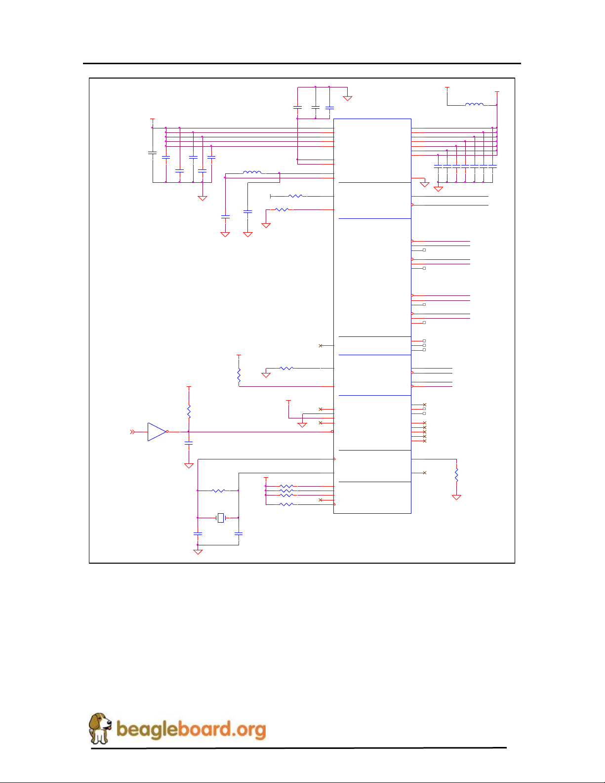
REF: BB_SRM_xM
BeagleBoard-xM System
Reference Manual
Revision C2
HUB_3V3
HUB_R ESET3
R106
10K
nHUB_R ESET
R105
100K
HUB_TMS
L11
2.0 Am p/0.05 DCR
1 2
USRBI AS
C184
4.7uF, 6.3V,0603
RXP
C178
33pF
R118
10K
C179
33pF
HUB_TDI
L10
2.0 Am p/0.05 DCR
1 2
RXN
CLK24_EN
C196
1uF,10V
HUB_TCK
TXP
U18B
SN74LVC2G06DC KR
3 4
HUB_3V3
R107 10K
TXN
R108 10K
HUB_3V3A
R109
12K,1%
R128 10K
R129 10K
USBDM_2
USBDP2
C197
0.1uF, 10V
USBDP_2
HUB_3V3
HUB_3V3
USBDP4USBDP_3
Upstream
Downstr eam
EEPROM
Pow er
Ethernet
Clocks
GPIO + Misc.
JTAG
U15
qf n64-11x27-smsc
LAN9514
USBDP0
59
USBDM0
58
USBDP2
2
USBDP3
4
USBDP4
7
USBDP5
9
USBDM2
1
USBDM3
3
USBDM4
6
USBDM5
8
VBUS_DET
11
PRTCTL2
14
PRTCTL3
16
PRTCTL4
17
PRTCTL5
18
EXRES
50
EEDO
25
EECS
24
EECLK
23
XI
61
XO
60
n_RESET
12
VDD33I O
33
VDD18U SBPLL
62
VDD33A
51
VDD18ETHPLL
48
VDD18C ORE
38
VSS(FLAG)
65
VDD33A
5
VDD33A
10
EEDI
26
VDD33I O
27
VDD33I O
19
VDD33A
54
VDD33A
57
VDD18C ORE
15
RXP
52
RXN
53
TXP
55
TXN
56
USBRBI AS
63
CLK24_EN
44
CLK24_OUT
45
AUTOMDIX_EN
41
nFDX_LED/GPIO0
20
nLNKA_LED/GPI O1
21
nSPD_LED/ GPIO2
22
GPIO3
35
GPIO4
36
GPIO5
37
GPIO6
42
GPIO7
43
TEST1
13
TEST2
34
TEST3
40
TEST4
47
VDD33I O
39
VDD33I O
46
VDD33A
49
VDD33A
64
nTRST
28
TMS
29
TDI
30
TDO
31
TCK
32
USBDM5USBDM_4
HUB_3V3
XI
VDD18ETHPLL
XO
HUB_VBU S
VDD18U SBPLL
AUTOMDIX_EN
VDD18C ORE
USBDM_3USBDM4
USBDM0
HUB_3V3
USBDM2
R101 100K
HUB_3V3
USBDP5USBDP_4
C1760.1uF, 10V
C1750.1uF, 10V
USBDP0
C185
0.1uF, 10V
C1910.1uF, 10V
C181
0.1uF, 10V
C1920.1uF, 10V
Y4
25.000MHz
xtal2-216x 60-hcm49
1 2
C182
0.1uF, 10V
C1740.1uF,10V
C1930.1uF, 10V
R112 1M
C187
1uF,10V
C1940.1uF, 10V
C180
0.1uF, 10V
C1950.1uF, 10V
R63
12.4K,1%,0603
HUB_nTRST
HUB_EXRES
C183
0.1uF, 10V
C186
0.1uF, 10V
C190
4.7uF, 6.3V,0603
The LAN9514/LAN9514i is a high performance Hi-Speed USB 2.0 hub with a 10/100
Ethernet controller. The LAN9514/LAN9514i contains an integrated USB 2.0 hub, four
integrated downstream USB 2.0 PHYs, an integrated upstream USB 2.0 PHY, a 10/100
Ethernet PHY, a 10/100 Ethernet Controller.
The main power supply for the LAN9514 is the HUB_3V3 supplied by the dedicated
power regulator. Filtering is required on all input pins. A 1.8V core voltage is derived
from an internal LDO and requires external filtering.
Figure 39. USB HUB Design
Page 81 of 163
Page 82
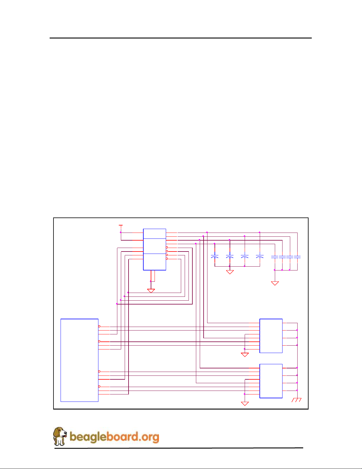
REF: BB_SRM_xM
BeagleBoard-xM System
Reference Manual
Revision C2
VBUS3
VBUS4
SHIELD
SHIELD
VBUSA
DADA+
GNDA
VBUSB
DBDB+
GNDB
SHIELD
SHIELD
P16
USB-A C onn.
A1
A3
A2
A4
MH1
MH2
B1
B2
B3
B4
MH3
MH4
VBUS1
+
C160
100UF
VBUS2
+
C161
100UF
U13
TPS2054BD
IN1
2
EN1
3
OUT1
15
OUT3
11
GND
1
IN2
6
OUT2
14
OC1
16
OUT4
10
GND
5
EN2
4
EN3
7
EN4
8
OC2
13
OC3
12
OC4
9
ESD_RI NG
VBUS3
+
C162
100UF
+
C163
100UF
VBUS4
SHIELD
SHIELD
VBUSA
DADA+
GNDA
VBUSB
DBDB+
GNDB
SHIELD
SHIELD
P14
USB-A C onn.
A1
A3
A2
A4
MH1
MH2
B1
B2
B3
B4
MH3
MH4
USBDP_2
USBDM_2
USBDP_1
C1730.1uF, 10V
DC_5V_U SB
C1720.1uF, 10V
C1710.1uF, 10V
USBDP_3
USBDM_4
USBDM_3
USBDM_1
USBDP_4
C1700.1uF, 10V
VBUS1
VBUS2
U15LAN 9514
USBDP2
2
USBDP3
4
USBDP4
7
USBDP5
9
USBDM2
1
USBDM3
3
USBDM4
6
USBDM5
8
PRTCTL2
14
PRTCTL3
16
PRTCTL4
17
PRTCTL5
18
The LAN9514 requires an external 25MHZ crystal to generate the required internal
clocks. The optional 24MHz clock output is not used on the board and is disabled.
The AUTOMIDX feature is enabled which allows for auto polarity detection. This
enables the port to automatically switch the TX and RX leads if needed.
7.14.4 USB Port Connectors
There a two dual port type A USB connectors used on the –xM board each one provides
connections for four signals, DP, DM, VBUS, and Ground. You will notice that there are
no external ESD devices on the connector. The ESD protection is integrated into the USB
HUB.
Figure 41 is the design of the power control for each USB host port. Each port can be
turned on or off from the LAN9514 over the USB interface. U13, a TPS2045, is a four
port FET with over current detection. The overcurrent detect output is tied to the enable
pin from the LAN9514. In an over current condition the signal is immediately turned off
without waiting for the processor to turn off the power. The LAN9514 detects the
overcurrent condition and keeps the over current condition turned off.
Figure 40. USB Port Power Design
Page 82 of 163
Page 83
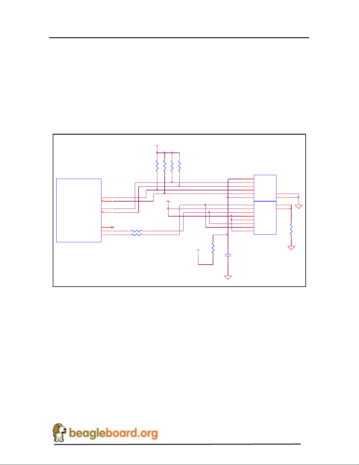
REF: BB_SRM_xM
BeagleBoard-xM System
Reference Manual
Revision C2
U15LAN9514
RXP
52
RXN
53
TXP
55
TXN
56
nFDX_LED/GPI O0
20
nLNKA_LED/ GPIO1
21
nSPD_LED/ GPIO2
22
HUB_3V3
R11449. 9,1%
HUB_3V3A
HUB_3V3
R11649. 9,1%
R11549. 9,1%
RXP
P15
ETHER
TCT
3
TD+
1
TD-
2
RD+
7
RD-
8
RCT
6
GND1
4
YELC
11
YELA
12
GRNC
9
GRNA
10
GND2
5
SHD1
13
SHD2
14
YEL+
18
YEL-
17
GRN+
15
GRN-
16
RXN
C198
0.022uF, 10V
R50 330
R104 330
TXP
TXN
R119
0,1210
nSPD
nLNKA
nLNKAR
R11049. 9,1%
nSPDR
R11710,1%
TCT_RCT
Each USB Host port has its own dedicated FET and power control. A 100uf capacitor is
connected to each USB power port for added surge current capabilities. A .1uf capacitor
is provided for bypass capacitance on each rail.
7.14.5 Ethernet
Figure 41 is the circuitry that applies to the Ethernet interface on the board. The
LAN9514 device while performing the function of the HUB also contains the Ethernet
controller.
The 10/100 Ethernet controller provides an integrated Ethernet MAC and PHY which are
fully IEEE 802.3 10BASE-T and 802.3u 100BASE-TX compliant. A connector, P15,
with integrated magnetics is used to provide the physical interface off the board. The
Ethernet features auto polarity correction and Auto-MIDX.
Figure 41. USB Based Ethernet Design
Page 83 of 163
Page 84
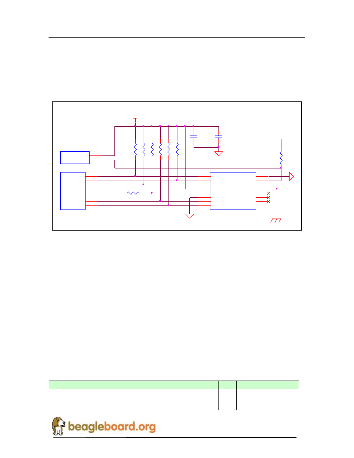
REF: BB_SRM_xM
BeagleBoard-xM System
Reference Manual
Revision C2
U4A
PROCESSOR
MMC 1_CLK
N28
MMC 1_CMD
M27
MMC 1_DAT0
N27
MMC 1_DAT1
N26
MMC 1_DAT2
N25
MMC 1_DAT3
P28
C144
10uF,C ER, 0805,6.3V
microSD
P7
SCHA2B0300
DAT2
1
CD/DAT3
2
CMD
3
VDD
4
CLOCK
5
VSS
6
DAT0
7
DAT1
8
GND
9
CD
10
GND3
11
GND4
12
TBD1
13
TBD2
14
TBD3
15
R7510K
VDD_MMC1
R7610K
R7710K
R7210K
R7310K
R7410K
C145
0.1uF, 10V
R135
10K
VIO_1V8
U7A TPS65950
CD1
P12
VMMC 1.OU T
C2
R16 33
Signal Name
Description
I/O
Pin
MMC1_CLK
SD/MMC Clock output.
O
N28
MMC1_CMD
SD/MMC Command pin
I/O
M27
MMC1_DAT(0..7)
SD/MMC Data pins
I/O
N27,N26,N25,P28,P27,
7.15 microSD
The board provides a single microSD interface. Its primary use is for providing the boot
source for SW. Unlike the BeagleBoard, it cannot be used for the typical SDIO or MMC
functions. Figure 42 is the microSD interface design on the BeagleBoard.
Figure 42. microSD Interface
7.15.1 microSD Power
The microSD connector is supplied power from the TPS65950 using the VMMC1 rail.
The default setting on this rail is 3.0V as set by the Boot ROM and under SW control, can
be set to 1.80V for use with 1.8V cards. The maximum current this rail can provide is
220mA as determined by the TPS65950 regulator. Maximum current can be limited by
the overall current available from the USB interface of the PC.
7.15.2 Processor Interface
There are no external buffers required for the microSD operation. The processor provides
all of the required interfaces for the microSD interface. Table 11 provides a description
of the signals on the MMC card.
Table 11. SD/MMC OMAP Signals
Page 84 of 163
Page 85

REF: BB_SRM_xM
BeagleBoard-xM System
Reference Manual
Revision C2
P26,R27,R25
7.15.3 Card Detect
When a card is inserted into the connector, the Card Detect pin is grounded. This is
detected on pin P12 of the TPS65950. An interrupt, if enabled, is sent to the processor
via the interrupt pin. The SW can be written such that the system comes out of sleep or a
reduced frequency mode when the card is detected.
7.15.4 Booting From SD/MMC Cards
The ROM code supports booting from the microSD cards with some limitations:
o Support for SD cards compliant with the Multimedia Card System Specification
v4.2 from the MMCA Technical Committee and the Secure Digital I/O Card
Specification v2.0 from the SD Association. Including high-capacity (size >2GB)
cards: HC-SD and HC MMC.
o 3-V power supply, 3-V I/O voltage on port 1
o Initial 1-bit MMC mode, 4-bit SD mode.
o Clock frequency:
– Identification mode: 400 kHz
– Data transfer mode: 20 MHz
o Only one card connected to the bus
o FAT12/16/32 support, with or without master boot sector (MBR).
The high-speed microSD host controllers handle the physical layer while the ROM code
handles the simplified logical protocol layer (read-only protocol). A limited range of
commands is implemented in the ROM code. The MMC/SD specification defines two
operating voltages for standard or high-speed cards. The ROM code only supports
standard operating voltage range (3-V). The ROM code reads out a booting file from the
card file system and boots from it.
Page 85 of 163
Page 86
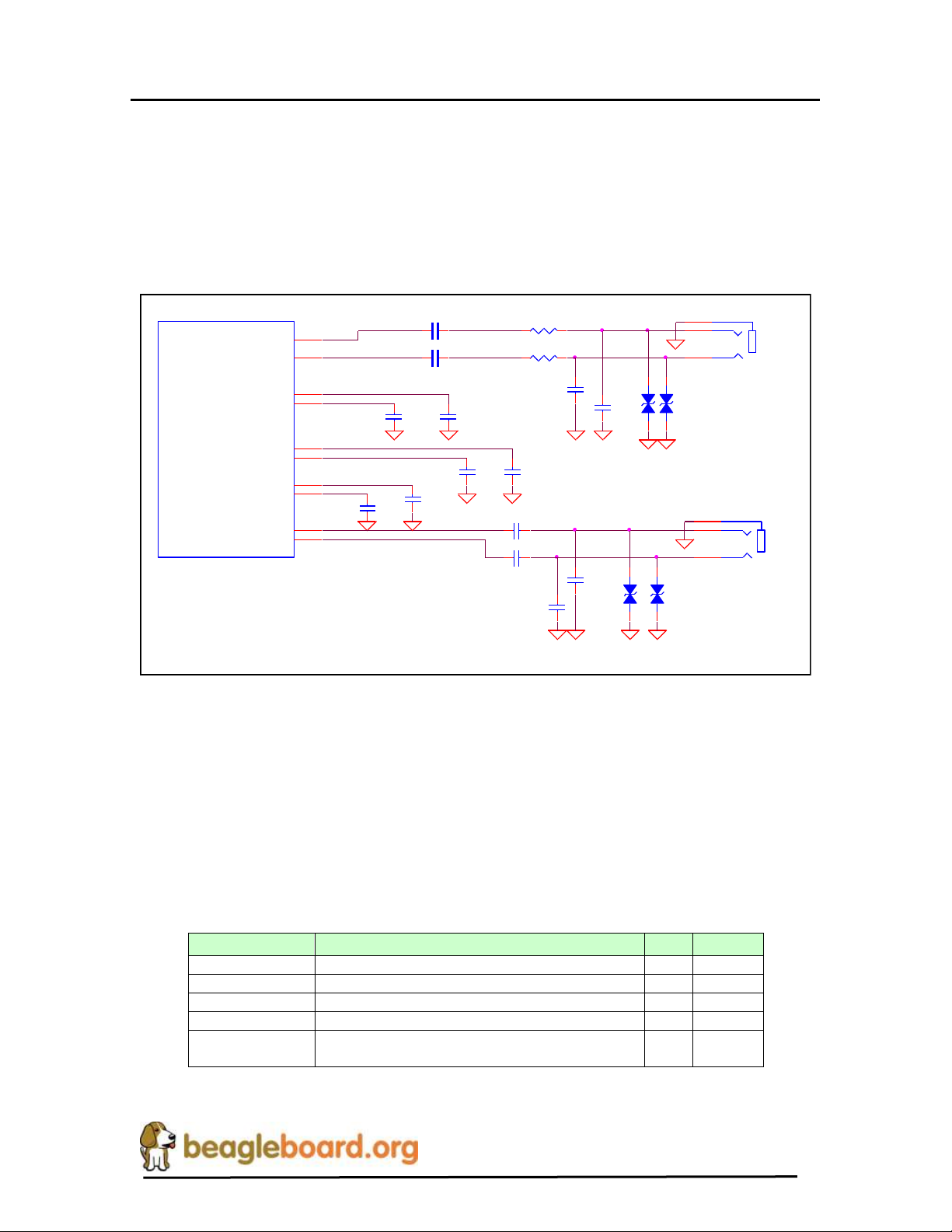
REF: BB_SRM_xM
BeagleBoard-xM System
Reference Manual
Revision C2
CONN _HSOL
CONN _HSOR
CONN _AUXR
DIG. MI C.0
C92
100pF
HSMIC. P
C95
100PF
DIG. MI C.1
HSMIC. M
C96
100PF
MIC.MAIN .M
C97
100PF
C94
100PF
INTER_H SOR
CONN _AUXLAUXL
C87 47uF, CER
HSOL
P6
1
2
3
P5
1
2
3
AUDIO_OUT
HSOR
C88 47uF, CER
INTER_H SOL
AUDIO_IN
AUXR
MIC.MAIN .P
D9
PGB0010603MR
C93
100pF
D8
PGB0010603MR
D10
PGB0010603MR
D11
PGB0010603MR
C99 0.1uF ,10V
C98 0.1uF, 10V
R58 33
R60 33
C90
47pF
C89
47pF
C100
47pF
C101
47pF
U7A TPS65950
AUXR
G1
AUXL
F1
HSMIC. M
F3
HSMIC. P
E3
MIC.MAIN .M
F2
HSOL
B4
HSOR
B5
MIC.MAIN .P
E2
MIC.SU B.P/D IG.MIC.0
G2
MIC.SU B.M/DI G.MIC1
H2
Signal Name
Description
I/O
Pin
mcbsp2_dr
Received serial data
I
R21
mcbsp2_dx
Transmitted serial data
I/O
M21
mcbsp2_clkx
Combined serial clock
I/O
N21
mcbsp2_fsx
Combined frame synchronization
I/O
P21
Mcbsp_clks
External clock input. Used to synchronize with
the TPS65950
I
T21
7.16 Audio Interface
The BeagleBoard supports stereo in and out through the TPS65950 which provides the
audio CODEC.
Figure 43 is the Audio circuitry design on the BeagleBoard.
Figure 43. Audio Circuitry
7.16.1 Processor Audio Interface
There are five McBSP modules called McBSP1 through McBSP5 on the processor.
McBSP2 provides a full-duplex, direct serial interface between CODEC inside the
TPS65950. It supports the I2S format to the TPS65950. In Table 12 are the signals used
on the processor to interface to the CODEC.
Table 12. Processor Audio Signals
Page 86 of 163
Page 87
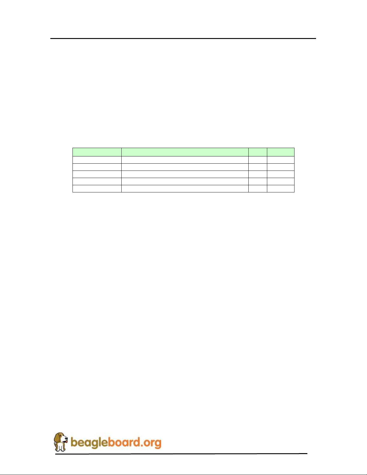
REF: BB_SRM_xM
BeagleBoard-xM System
Reference Manual
Revision C2
Signal Name
Description
I/O
Pin
I2S.CLK
Clock signal (audio port)
I/O
L3
I2S.SYNC
Synchronization signal (audio port)
IO
K6
I2S.DIN
Data receive (audio port)
I
K4
I2S. DOUT
Data transmit (audio port)
O
K3
CLK256FS
Synchronization frame sync to the PROCESSOR
O
D13
7.16.2 TPS65950 Audio Interface
The TPS65950 acts as a master or a slave for the I2S interface. If the TPS65950 is the
master, it must provide the frame synchronization (I2S_SYNC) and bit clock (I2S_CLK)
to the processor. If it is the slave, the TPS65950 receives frame synchronization and bit
clock. The TPS65950 supports the I2S left-justified and right-justified data formats, but
doesn’t support the TDM slave mode.
In Table 13 are all the signals used to interface to the processor.
Table 13. Processor Audio Signals
A new feature on the –xM is the ability to access the audio signals for use on an external
add on board. If this feature is to be used, you must disable via SW this interface on the
TPS65950.
7.16.3 Audio Output Jack
A single 3.5mm jack is provided on BeagleBoard to support external stereo audio output
devices such as headphones and powered speakers. This interface is not amplified and
may require the use of amplified speakers in certain instances.
7.16.4 Audio Input Jack
A single 3.5mm jack is supplied to support external audio inputs including stereo or
mono. If a microphone is o be used, it may require additional amplification of the signal
for proper use.
Page 87 of 163
Page 88
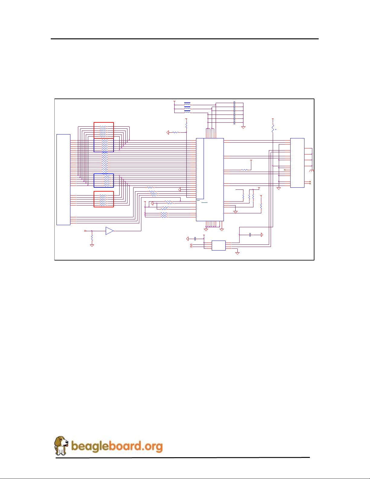
REF: BB_SRM_xM
BeagleBoard-xM System
Reference Manual
Revision C2
R95 R ES_0_0402,DNI
R92
4.7K
R96 R ES_0_0402,DNI
RP1F 106 11
R97 R ES_0_0402,DNI
AUX_3V3
TVDD
RP2C 103 14
RP2E 105 12
RP2D 104 13
R94 10K
RP2F 106 11
DVI_DATA19
R43
10K
DVI_UP3
AUX_3V3
Insures that the
DVI-D is
powered down
at powerup.
R93
10K
U5B
SN74LVC2G07DBVR
3 4
RP4E 105 12
RP4F 106 11
RP4H 108 9
RP4G 107 10
AUX_3V3
MSEN
C153 0.1uF,10V
t
RT1
PTC_RXEF010
C154 0.1uF,10V
AUX_3V3
DVI_DATA20
DC_5V
VIO_1V8
R89
4.7K
RP7H 108 9
RP7C 103 14
RP7F 106 11
RP7D 104 13
RP7G 107 10
RP7E 105 12
DVI_DATA21
RP1A 101 16
R91
1K
DDC_I2C 3_SCL
DVI_DATA0
RP2H 108 9
I2C3_SCL4
C156 0.1uF,10V
VIO_1V8
DVI_DATA22
RP4A 101 16
RP3A 101 16
RP3C 103 14
RP3B 102 15
RP3E 105 12
RP3D 104 13
RP3G 107 10
RP3F 106 11
RP3H 108 9
DVI_DATA1
R88
1K
I2C3_SDA4
DVI_DATA2
U11
TFP410
PD0
63
PD1
62
PD2
61
PD3
60
PD4
59
PD5
58
PD6
55
PD7
54
PD8
53
PD9
52
PD10
51
PD11
50
PD12
47
PD13
46
PD14
45
PD15
44
PD16
43
PD17
42
PD18
41
PD19
40
PD20
39
PD21
38
PD22
37
PD23
36
TXD0+
25
TXD0-
24
TXD1+
28
TXD1-
27
TXD2+
31
TXD2-
30
TFADJ
19
TXC+
22
TXC-
21
DK2
7
DK1
8
IDCK+
57
IDCK-
56
DE
2
VSYNC
5
HSYNC
4
BSEL/SCL
15
DSEL/SDA
14
HTPLG
9
NC
49
RSVD2
34
DKEN
35
VREF
3
TGND32TGND26TGND
20
DVDD33DVDD
12
DGND16PGND
17
PVDD18TVDD23TVDD
29
DGND
48
MSEN
11
DK3
6
ISEL/RESET
13
PD
10
DVDD
1
DGND64TP
65
DDC_I2C 3_SDA
I2C3_SCL
R84
8.45K_1%_0603
DVI_DATA3
I2C3_SDA
RP1B 102 15
R85 8. 06K_1%_0603
DVI_DATA4
DVI_DATA23
DVI_DATA5
RP4B 102 15
RP4C 103 14
RP4D 104 13
RP2G 107 10
RP5B 102 15
RP5A 101 16
RP5D 104 13
RP5C 103 14
RP5F 106 11
RP5E 105 12
DVI_DEN
DVI_DATA10
DVI_+5v
VIO_1V8
DVI_DATA16
BSEL
TXD0-
ISEL
TXD2+
DVI_CLK+
R86 10K
U12
TXS0102DCU
A15B1
8
VCCA3VCCB
7
OE6GND
2
A24B2
1
TXC+
DVI_DSEL
DVI_DATA15
TFADJ
DVI_DATA11
DVI_VSYN C
TXD1+
TVDD
DVI_DATA14
TXD0+
RP1C 103 14
DVI_DATA12
DVI_DATA17
TXD2-
DVI_PVDD
410_NC
DVI_DATA7
DVI_DATA8
TXC-
DKEN
DVI_DVDD
DVI_HSY NC
C158 0.1uF,10V
TXD1-
DVI_DATA6
DVI_PUP
DVI_DATA9
DVI_VREF
HTPLG
DVI_DATA13
C159 0.1uF,10V
P12
CONN_HD MI
DAT2+
1
DAT2-
3
DAT2_S
2
DAT1+
4
DAT1_S
5
DAT1-
6
DAT0+
7
DAT0_S
8
DAT0-
9
CLK+
10
CLK-
12
CLK_S11CEC
13
NC
14
SCL
15
SDA
16
DDC/C EC GND
17
+5V
18
HPLG
19
MTG1
MTG1
MTG2
MTG2
MTG3
MTG3
MTG4
MTG4
RP1D 104 13
R90 10K
L7 FERRITE, MMZ1608R301A1 2
DDC I2C Interface
Adjusted for .9V
Internal 10K Pullups .
L8 FERRITE, MMZ1608R301A1 2
R87
510
L9 FERRITE, MMZ1608R301A1 2
C152 0.1uF,10V
RP1E 105 12
DK3
C157 0.1uF,10V
DK1
DK2
100Ma
DVI_DATA18
C155 0.1uF,10V
U4AProcessor
DSS_D0
AG22
DSS_D1
AH22
DSS_D2
AG23
DSS_D3
AH23
DSS_D4
AG24
DSS_D5
AH24
DSS_D6
E26
DSS_D7
F28
DSS_D8
F27
DSS_D9
G26
DSS_D10
AD28
DSS_D11
AD27
DSS_D12
AB28
DSS_D13
AB27
DSS_D14
AA28
DSS_D15
AA27
DSS_D16
G25
DSS_D17
H27
DSS_PCLK
D28
DSS_HSYN C
D26
DSS_VSYNC
D27
DSS_ACBIAS
E27
DSS_D18
H26
DSS_D19
H25
DSS_D20
E28
DSS_D21
J26
DSS_D22
AC27
DSS_D23
AC28
DSS_D18
AH26
DSS_D19
AG26
DSS_D20
AF18
DSS_D21
AF19
DSS_D22
AE21
DSS_D23
AF21
7.17 DVI-D Interface
The LCD interface on the processor is accessible from the DVI-D interface connector on
the board. Figure 44 is the DVI-D interface design.
One of the main changes in the DSS area on the –xM is the change of the DSS pin usage.
The processor requires that different pins be used if 720p resolutions are required. These
pins are different than those that are currently used on the BeagleBoard. The basic change
requires that the DSS_D0-D5 need to be moved to the pins that normally carry the
DSS_D18-D23 leads. In this case, the signals for DSS_D18-D23 need to be moved to
other pins. Reflected in Figure 44 are four resistor packs inside either Red or Blue boxes.
These are the loading options to enable the new mode used by the –xM or the legacy
mode used by the BeagleBoard. The resistor packs in the RED boxes are installed and the
BLUE boxes are not installed on the –xM to support the 720p resolution.
For legacy operation, you would need to install the BLUE boxes and leave out the RED
boxes. The SW will take care of this automatically, but you may want to do this if your
design were to need to work in the legacy mode.
Figure 44. DVI-D Interface
Page 88 of 163
Page 89
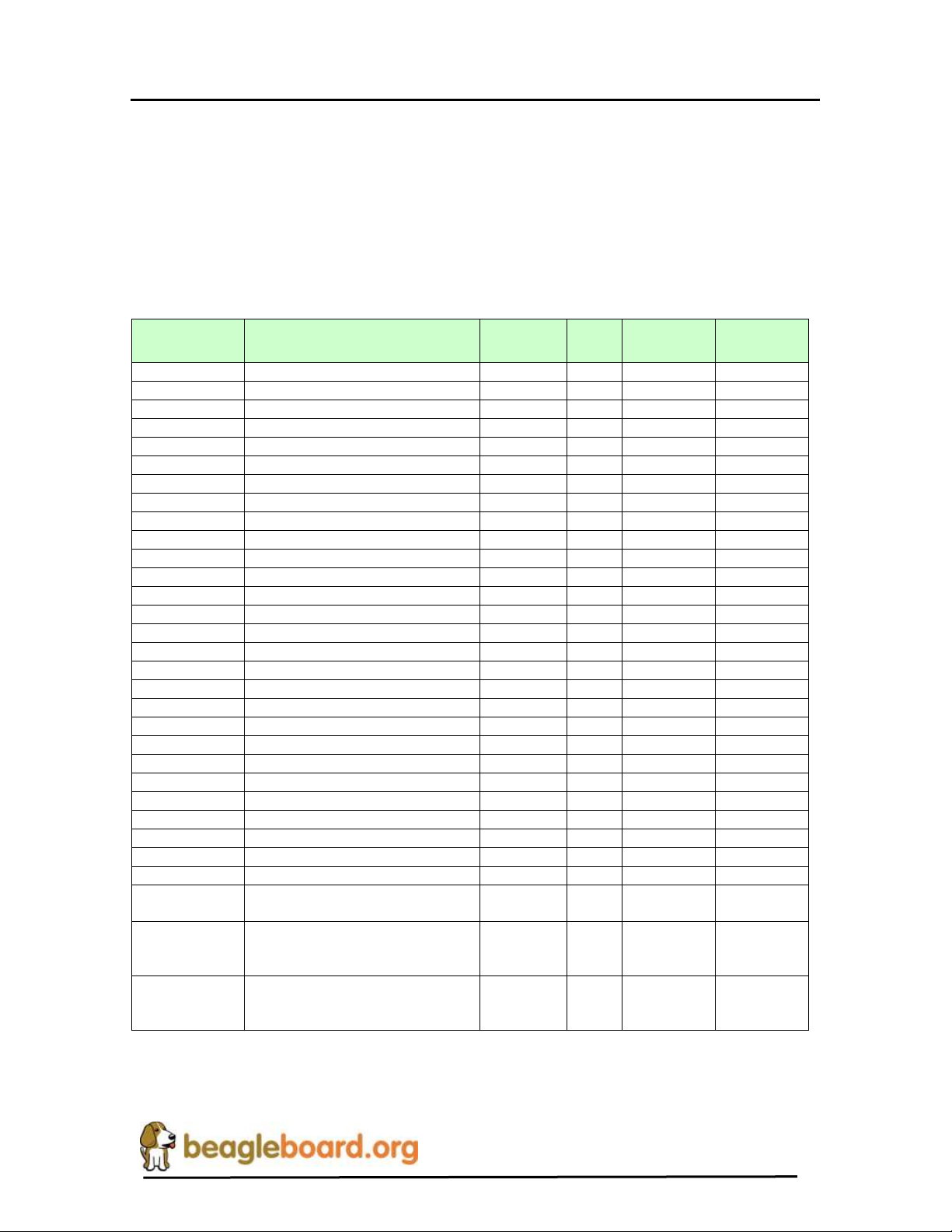
REF: BB_SRM_xM
BeagleBoard-xM System
Reference Manual
Revision C2
Signal
Description
Type
Ball
(Legacy)
Ball
(720p)
dss_pclk
LCD Pixel Clock
O D28
D28
dss_hsync
LCD Horizontal Synchronization
O D26
D26
dss_vsync
LCD Vertical Synchronization
O D27
D27
dss_acbias
Pixel data enable (TFT) output
O E27
E27
dss_data0
LCD Pixel Data bit 0
BLUE0
O
AG22
H26
dss_data1
LCD Pixel Data bit 1
BLUE1
O
AH22
H25
dss_data2
LCD Pixel Data bit 2
BLUE2
O
AG23
E28
dss_data3
LCD Pixel Data bit 3
BLUE3
O
AH23
J26
dss_data4
LCD Pixel Data bit 4
BLUE4
O
AG24
AC27
dss_data5
LCD Pixel Data bit 5
BLUE5
O
AH24
AC28
dss_data6
LCD Pixel Data bit 6
BLUE6
O
E26
E26
dss_data7
LCD Pixel Data bit 7
BLUE7
O
F28
F28
dss_data8
LCD Pixel Data bit 8
GREEN0
O
F27
F27
dss_data9
LCD Pixel Data bit 9
GREEN1
O
G26
G26
dss_data10
LCD Pixel Data bit 10
GREEN2
O
AD28
AD28
dss_data11
LCD Pixel Data bit 11
GREEN3
O
AD27
AD27
dss_data12
LCD Pixel Data bit 12
GREEN4
O
AB28
AB28
dss_data13
LCD Pixel Data bit 13
GREEN5
O
AB2
AB2
dss_data14
LCD Pixel Data bit 14
GREEN6
O
AA28
AA28
dss_data15
LCD Pixel Data bit 15
GREEN7
O
AA27
AA27
dss_data16
LCD Pixel Data bit 16
RED0
O
G25
G25
dss_data17
LCD Pixel Data bit 17
RED1
O
H27
H27
dss_data18
LCD Pixel Data bit 18
RED2
O
H26
AH26
dss_data19
LCD Pixel Data bit 19
RED3
O
H25
AG26
dss_data20
LCD Pixel Data bit 20
RED4
O
E28
AF18
dss_data21
LCD Pixel Data bit 21
RED5 O J26
AF19
dss_data22
LCD Pixel Data bit 22
RED6
O
AC27
AE21
dss_data23
LCD Pixel Data bit 23
RED7
O
AC28
AF21
GPIO_170
Powers down the TFP410 when
Lo. TFP410 is active when Hi.
O J25
I2C3_SCL
I2C3 clock line. Used to
communicate with the monitor to
determine setting information.
I/O
AF14
AF14
I2C3_SDA
I2C3 data line. Used to
communicate with the monitor to
determine setting information.
I/O
AG14
AG14
7.17.1 Processor LCD Interface
The main driver for the DVI-D interface originates at the processor via the DSS pins. The
PROCESSOR provides 24 bits of data to the DVI-D framer chip, TFP410. There are
three other signals used to control the DVI-D that originate at the processor. These are
I2C3_SCL, I2C3_SDA, and GPIO_170. All of the signals used are described in Table
14.
Table 14. Processor LCD Signals
10ohm series resistors are provide in the signal path to minimize reflections in the high
frequency signals from the processor to the TFP410. These resistors are in the form of
Page 89 of 163
Page 90
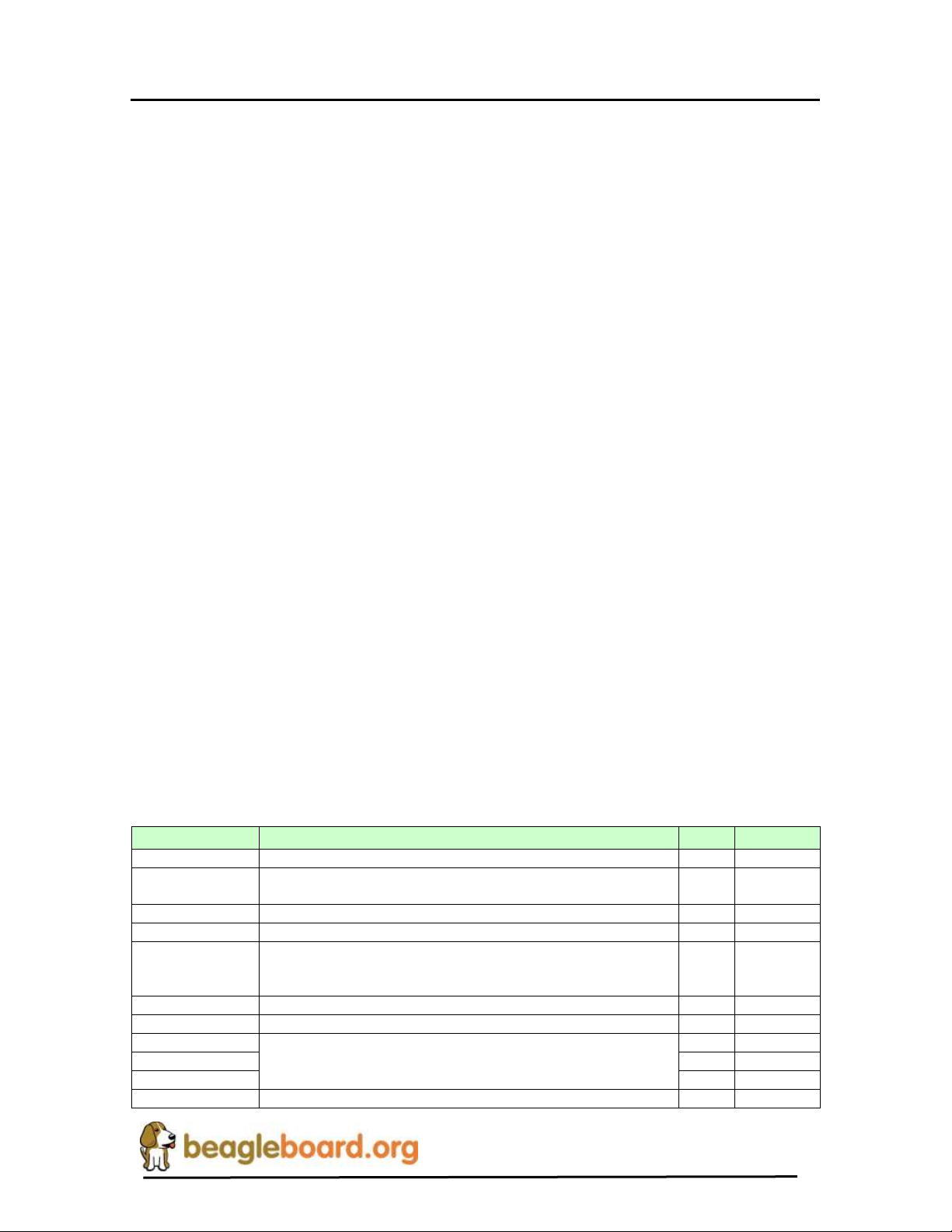
REF: BB_SRM_xM
BeagleBoard-xM System
Reference Manual
Revision C2
Signal Name
Description
Type
Ball
DATA[23:12]
The upper 12 bits of the 24-bit pixel bus.
I
36–47
DATA[11:0]
The bottom 12 bits of the 24-bit pixel bus.
I
50–55.56-
53
IDCK+
Single ended clock input.
I
57
IDCK-
Tied to ground to support the single ended mode.
I
56
DE
Data enable. During active video (DE = high), the transmitter
encodes pixel data, DATA[23:0]. During the blanking interval
(DE = low), the transmitter encodes HSYNC and VSYNC.
I
2
HSYNC
Horizontal sync input
I 4 VSYNC
Vertical sync input
I 5 DK3
These three inputs are the de-skew inputs DK[3:1], used to
adjust the setup and hold times of the pixel data inputs
DATA[23:0], relative to the clock input IDCK±.
I 6 DK2 I 7
DK1 I 8
A low level indicates a powered on receiver is detected at the
resistor packs on the BeagleBoard. The maximum clock frequency of these signals is
65MHz.
It should be noted that on the Rev A2 version, the ability to shut off the DVI-D display is
not supported. This will be fixed on the next letter revision of the board.
7.17.2 LCD Power
In order for the DSS outputs to operate correctly out of the processor, two voltage rails
must be active, VIO_1V8 and VDD_PLL2. Both of these rails are controlled by the
TPS65950 and must be set to 1.8V. By default, VDD_PLL2 is not turned and must be
activated by SW. Otherwise some of the bits will not have power supplied to them.
7.17.3 TFP410 Power
Power to the TFP410 is supplied from the 3.3V regulator in U1, the TPS2141. In order to
insure a noise free signal, there are three inductors, L4, L5, and L6 that are used to filter
the 3.3V rail into the TFP410.
7.17.4 TFP410 Framer
The TFP410 provides a universal interface to allow a glue-less connection to provide the
DVI-D digital interface to drive external LCD panels. The adjustable 1.1-V to 1.8-V
digital interface provides a low-EMI, high-speed bus that connects seamlessly with the
1.8V and 24-bit interface output by the processor. The DVI interface on the BeagleBoard
supports flat panel display resolutions up to XGA at 65 MHz in 24-bit true color pixel
format.
Table 15 is a description of all of the interface and control pins on the TFP410 and how
they are used on BeagleBoard.
Table 15. TFP410 Interface Signals
Page 90 of 163
Page 91
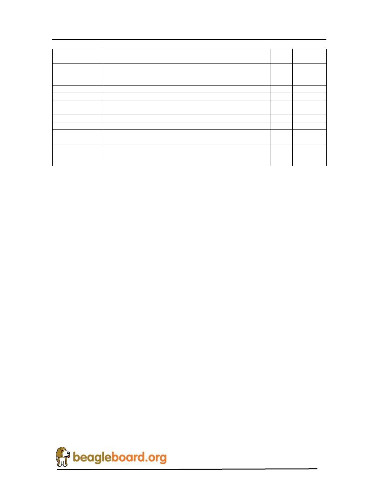
REF: BB_SRM_xM
BeagleBoard-xM System
Reference Manual
Revision C2
MSEN
differential outputs. A high level indicates a powered on
receiver is not detected.
O
11
ISEL
This pin disables the I2C mode on chip. Configuration is
specified by the configuration pins (BSEL, DSEL, EDGE,
VREF) and state pins (PD, DKEN).
I
13
BSEL
Selects the 24bit and single-edge clock mode.
I
13
DSEL
Lo to select the single ended clock mode.
I
14
EDGE
A high level selects the primary latch to occur on the rising edge
of the input clock IDCK
I
9
DKEN
A HI level enables the de-skew controlled by DK[1:3]
I
35
VREF
Sets the level of the input signals from the PROCESSOR.
I
3
PD
A HI selects normal operation and a LO selects the powerdown
mode.
I
10
TGADJ
This pin controls the amplitude of the DVI output voltage
swing, determined by the value of the pullup resistor RTFADJ
connected to 3.3V.
I
19
7.17.5 TFP410 Control Pins
There are twelve control pins that set up the TFP410 to operate with the processor. Most
of these pins are set by HW and do not require any intervention by the processor to set
them.
7.17.5.1 ISEL
The ISEL pin is pulled LO via R99 to place the TFP410 in the control pin mode with the
I2C feature disabled. This allows the other modes for the TFP410 to be set by the other
control pins.
7.17.5.2 BSEL
The BSEL pin is pulled HI to select the 24 bit mode for the Pixel Data interface from the
processor.
7.17.5.3 DSEL
The DSEL pin is pulled low to select the single ended clock mode from the
PROCESSOR.
7.17.5.4 EDGE
The EDGE signal is pulled HI through R82 to select the rising edge on the IDCK+ lead
which is the pixel clock from the PROCESSOR.
7.17.5.5 DKEN
The DKEN signal is pulled HI to enable the de-skew pins. The de-skew pins, DK1-DK3,
are pulled low by the internal pulldown resistors in the TFP410. This is the default mode
Page 91 of 163
Page 92

REF: BB_SRM_xM
BeagleBoard-xM System
Reference Manual
Revision C2
of operation. If desired, the resistors can be installed to pull the signals high. However, it
is not expected that any of the resistors will need to be installed. The DK1-DK3 pins
adjust the timing of the clock as it relates to the data signals.
7.17.5.6 MSEN
The MSEN signal, when low, indicates that there is a powered monitor plugged into the
DVI-D connector. This signal is not connected to the processor and is provided as a test
point only.
7.17.5.7 VREF
The VREF signal sets the voltage level of the DATA, VSYNC, HSYNC, DE, and
IDCK+ leads from the processor. As the processor is 1.8V, the level is set to .9V by R64
and R65.
7.17.5.8 PD
The PD signal originates from the processor on the GPIO_170 pin. Because the PD
signal on the TFP410 is 3.3V referenced, this signal must be converted to 3.3V. This is
done by U4, SN74LVC2G07, a non-inverting open drain buffer. If the GPIO_170 pin is
HI, then the open drain signal is inactive, causing the signal to be pulled HI by R98.
When GPIO_170 is taken low, the output of U4 will also go LO, placing the TFP410 in
the power down mode. Even though U4 is running at 1.8V to match the processor, the
output will support being pulled up to 3.3V. On power up, the TFP410 is disabled by
R109, a 10K resistor. When the processor powers on, pin J25 comes in the safe mode,
meaning it is not being driven. R109 insures that the signal is pulled LO, putting the
TFP410 in the power down mode.
7.17.5.9 TFADJ
The TFADJ signal controls the amplitude of the DVI output voltage swing, determined
by the value of R95.
7.17.5.10 RSVD2
This unused pin is terminated to ground as directed by the TFP410 data manual.
7.17.5.11 NC
This unused pin is pulled HI as directed by the TFP410 data manual.
7.17.6 DVI-D Connector
Page 92 of 163
Page 93

REF: BB_SRM_xM
BeagleBoard-xM System
Reference Manual
Revision C2
In order to minimize board size, a HDMI connector was selected for the DVI-D
connection. The BeagleBoard does not support HDMI but only the DVI-D component of
HDMI. The Cable is not supplied with the BeagleBoard but is available from numerous
cable suppliers and is required to connect a display to the BeagleBoard.
7.17.6.1 Shield Wire
Each signal has a shield wire that is used in the cable to provide signal protection for each
differential pair. This signal is tied directly to ground.
7.17.6.2 DAT0+/DAT0-
The differential signal pair DAT0+/DAT0- transmits the 8-bit blue pixel data during
active video and HSYNC and VSYNC during the blanking interval.
7.17.6.3 DAT1+/DAT1-
The differential signal pair DAT1+/DAT1- transmits the 8-bit green pixel data during
active video.
7.17.6.4 DAT2+/DAT2-
The differential signal pair DAT2+/DAT2- transmits the 8-bit red pixel data during
active.
7.17.6.5 TXC+/TXC-
The differential signal pair TXC+/TXC- transmits the differential clock from the
TFP410.
7.17.6.6 DDC Channel
The Display Data Channel or DDC (sometimes referred to as EDID Enhanced Display
ID) is a digital connection between a computer display and the processor that allows the
display specifications to be read by the processor. The standard was created by the Video
Electronics Standards Association (VESA). The current version of DDC, called DDC2B,
is based on the I²C bus. The monitor contains EEPROM programmed by the
manufacturer with information about the graphics modes that the monitor can display.
This interface in the LCD panel is powered by the +5V pin on the connector through
RT1, a resetable fuse. As the processor is 1.8V I/O, the I2C bus is level translated by
U11, a TXS0102. It provides for a split rail to allow the signals to interface on both sides
of the circuit. Inside of TXS0102 is a pullup on each signal, removing the need for an
external resistor.
7.17.6.7 HDMI Support
Page 93 of 163
Page 94
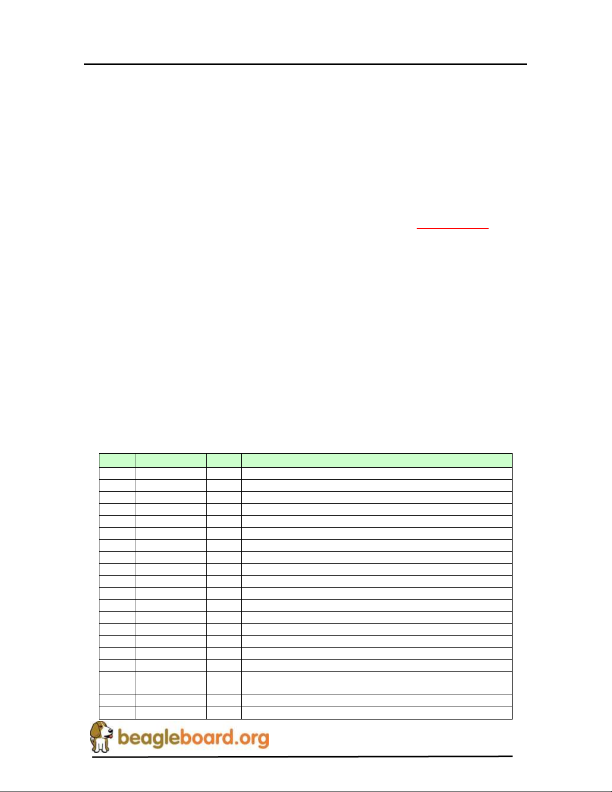
REF: BB_SRM_xM
BeagleBoard-xM System
Reference Manual
Revision C2
Pin#
Signal
I/O
Description
1
DC_5V
PWR
DC rail from the Main DC supply
2
DC_5V
PWR
DC rail from the Main DC supply
3
DVI_DATA1
O
LCD Pixel Data bit
4
DVI_DATA0
O
LCD Pixel Data bit
5
DVI_DATA3
O
LCD Pixel Data bit
6
DVI_DATA2
O
LCD Pixel Data bit
7
DVI_DATA5
O
LCD Pixel Data bit
8
DVI_DATA4
O
LCD Pixel Data bit
9
DVI_DATA12
O
LCD Pixel Data bit
10
DVI_DATA10
O
LCD Pixel Data bit
11
DVI_DATA23
O
LCD Pixel Data bit
12
DVI_DATA14
O
LCD Pixel Data bit
13
DVI_DATA19
O
LCD Pixel Data bit
14
DVI_DATA22
O
LCD Pixel Data bit
15
I2C3_SDA
I/O
I2C3 Data Line
16
DVI_DATA11
O
LCD Pixel Data bit
17
DVI_VSYNC
O
LCD Vertical Sync Signal
18
DVI_PUP
O
Control signal for the DVI controller. When Hi, DVI is enabled.
Can be used to activate circuitry on adapter board if desired.
19
GND
PWR
Ground bus
20
GND
PWR
Ground bus
The digital portion of the DVI-D interface is compatible with HDMI and is electrically
the same. A standard HDMI cable may be used to connect to the HDMI input of monitors
or televisions. Whether or not the Beagle will support those monitors is dependent on the
timings that are used on the BeagleBoard and those that are accepted by the monitor. This
may require a change in the software running on the Beagle. The audio and encryption
features of HDMI are not supported by the BeagleBoard.
7.17.6.8 DVI to VGA
The analog portion of DVI, which provides RGB analog signals, is not supported by the
BeagleBoard. Buying a DVI to VGA adapter connector will not work on a VGA display.
You will need an active DVI-D to VGA adapter. Another option for these signals is to
buy a board that connects to the J4 and J5 expansion connectors and generates the RGB
signals for the VGA display.
7.18 LCD Expansion Headers
Access is provided on the -XM Rev A to allow access to the LCD signals. Table 16
shows the signals that are on the P11 connector. You will notice that the signals are not in
a logical order or grouping. This is due to the routing on the PCB where we allowed the
routing to take precedence to get it to route with no addition of layers to the design.
Table 16. P11 LCD Signals
Page 94 of 163
Page 95
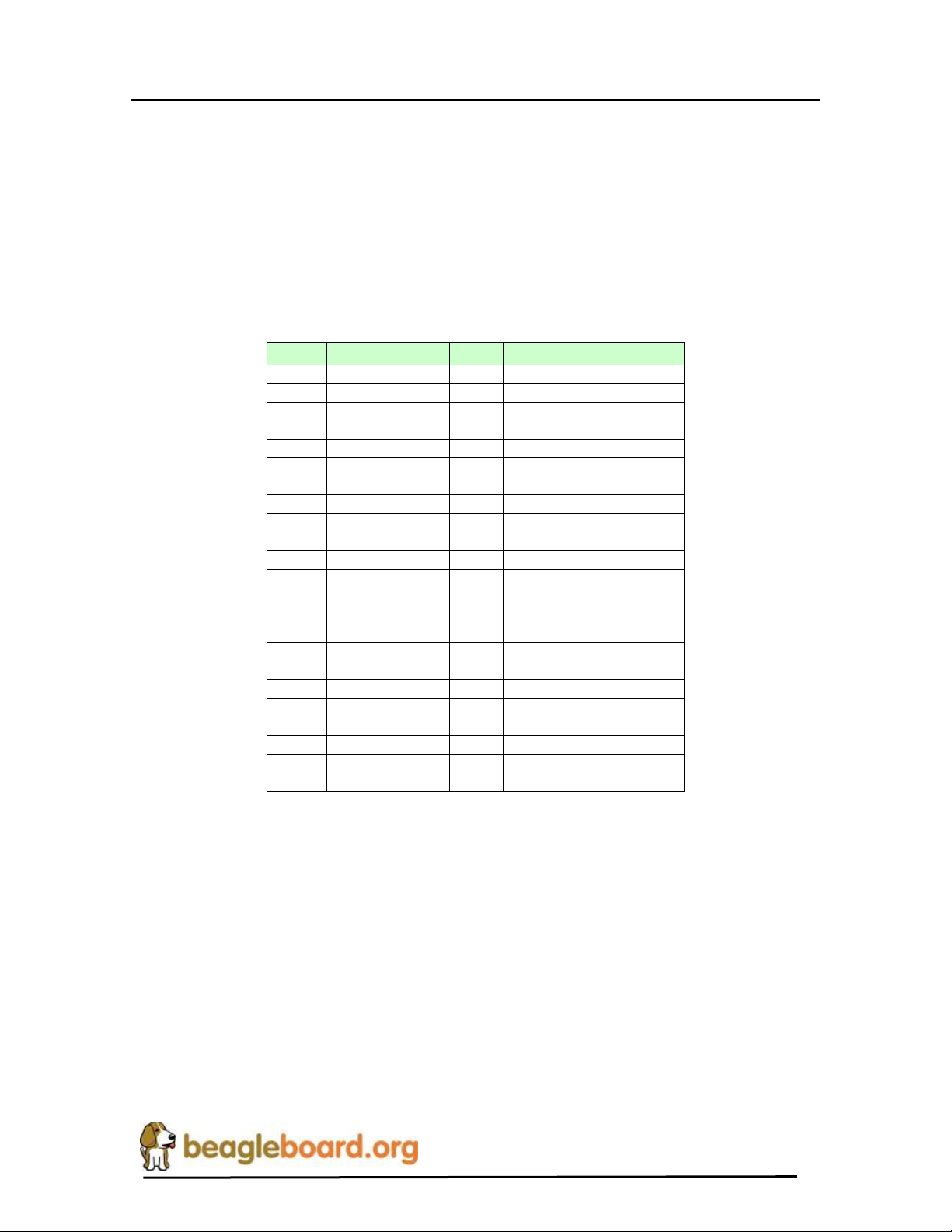
REF: BB_SRM_xM
BeagleBoard-xM System
Reference Manual
Revision C2
Pin#
Signal
I/O
Description
1
3.3V
PWR
3.3V reference rail
2
VIO_1V8
PWR
1.8V buffer reference rail.
3
DVI_DATA20
O
LCD Pixel Data bit
4
DVI_DATA21
O
LCD Pixel Data bit
5
DVI_DATA17
O
LCD Pixel Data bit
6
DVI_DATA18
O
LCD Pixel Data bit
7
DVI_DATA15
O
LCD Pixel Data bit
8
DVI_DATA16
O
LCD Pixel Data bit
9
DVI_DATA7
O
LCD Pixel Data bit
10
DVI_DATA13
O
LCD Pixel Data bit
11
DVI_DATA8
O
LCD Pixel Data bit
12
nUSB_PWR
O
LO indicates power is
from the USB port. HI
indicates that power is
from the DC jack.
13
DVI_DATA9
LCD Pixel Data bit
14
I2C3_SCL
I/O
I2C3 Clock Line
15
DVI_DATA6
O
LCD Pixel Data bit
16
DVI_CLK+
O
DVI Clock
17
DVI_DEN
O
Data Enable
18
DVI_HSYNC
O
Horizontal Sync
19
GND
PWR
Ground bus
20
GND
PWR
Ground bus
The current available on the DC_5V rail is limited to the available current that remains
from the DC supply that is connected to the DC power jack on the board. Keep in mind
that some of that power is needed by the USB Host power rail and if more power is
needed for the expansion board, the main DC power supply current capability may need
to be increased. All signals are 1.8V except the DVI_PUP which is a 3.3V signal.
Table 17 shows the signals that are on connector P13.
Table 17. P13 LCD Signals
The 1.8V rail is for level translation only and should not be used to power circuitry on the
board. The 3.3V rail also has limited capacity on the power as well. If the TFP410 is
disabled on the Beagle, then 80mA is freed up for use on an adapter card connected to the
LCD signals connectors. It is not required that the TFP410 be disabled when running an
adapter card, but the power should be taken into consideration when making this
decision.
It is suggested that the 5V rail be used to generate the required voltages for an adapter
card.
Page 95 of 163
Page 96
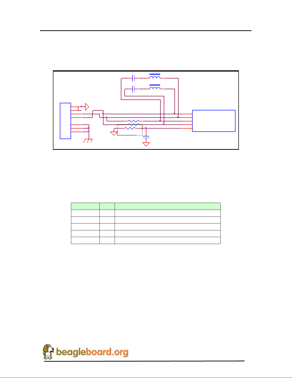
REF: BB_SRM_xM
BeagleBoard-xM System
Reference Manual
Revision C2
R34 0,DN I
P4
CONN_SVideo
P1
1
P2
2
P3
3
P4
4
5
MH1
6
MH2
7
MH3
C9
0.1uF, 10V
L2
3.3uH
1 2
L3
3.3uH
1 2
R33 1.65K,1%
R32 1.65K,1%
C11
47pF
C10
47pF
U4BProcess or
TV_OUT2
W28
TV_OUT1
Y28
TV_VFB1
Y27
TV_VREF
W26
TV_VFB2
W27
Signal
I/O
Description
tv_out1
O
TV analog output composite
tv_out2
O
TV analog output S-VIDEO
tv_vref
I
Reference output voltage from internal bandgap
tv_vfb1
O
Amplifier feedback node
tv_vfb2
O
Amplifier feedback node
7.19 S-Video
A single S-Video port is provided on the BeagleBoard. Figure 45 is the design of the SVideo interface.
Figure 45. S-Video Interface
Table 18 is the list of the signals on the S-Video interface and their definitions.
Table 18. S-Video Interface Signals
Power to the internal DAC is supplied by the TPS65950 via the VDAC_1V8 rail. Figure
37 reflects the filtering that is used on these rails, including the input VBAT rail.
A 47pf CAP and 3.3uh inductor are across the feedback resistors to improve the quality
of the S-Video signal.
7.20 Camera Port
A new addition to the –xM is the camera port. This camera port uses the native camera
interface of the processor. The connector configuration is designed to be compatible with
the camera modules from Leopard Imaging. USB cameras may also be used if desired,
but this interface has many HW assisted features and can support camera modules from
VGA to 5MP resolutions. Figure 46 is the Camera interface design.
Page 96 of 163
Page 97
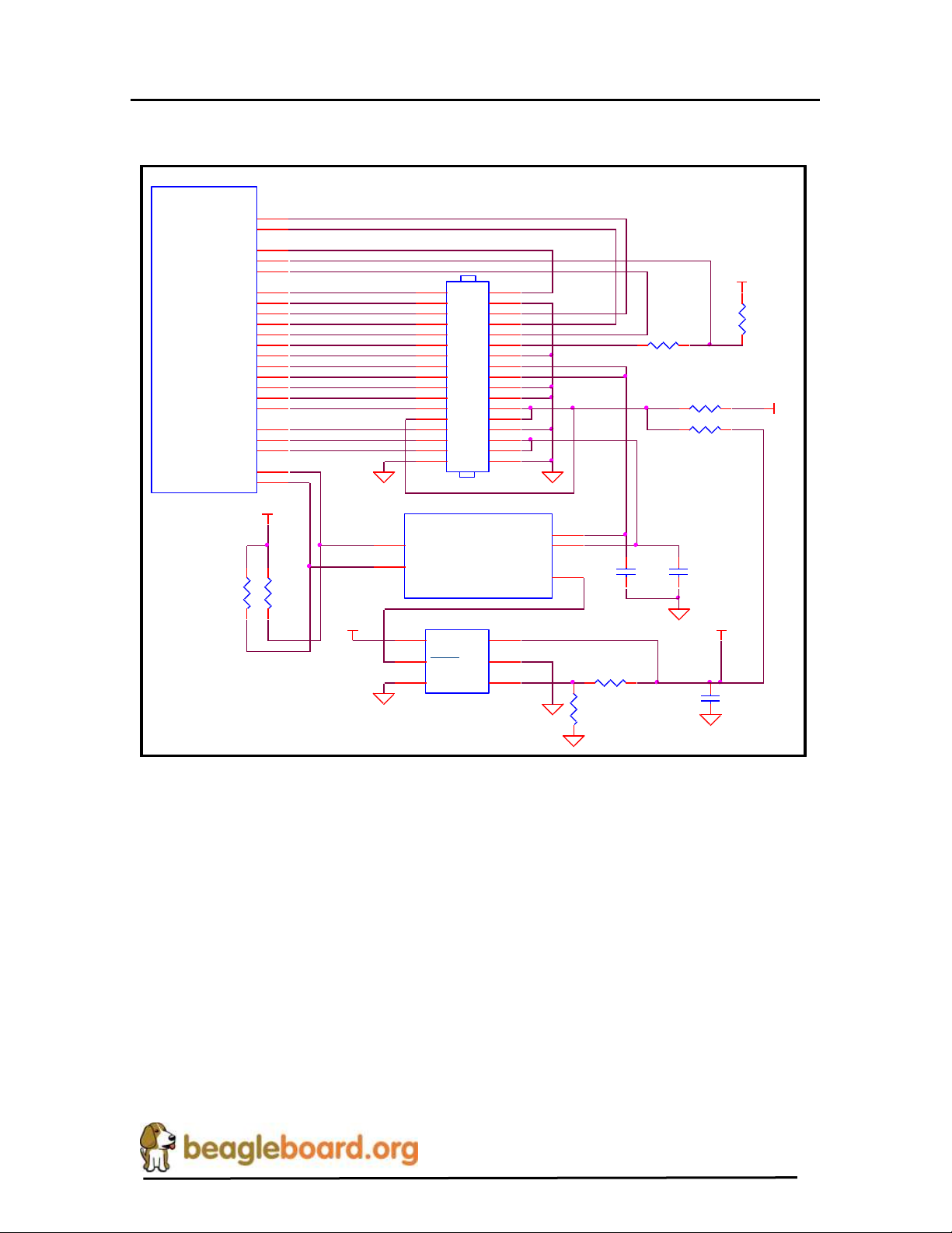
REF: BB_SRM_xM
BeagleBoard-xM System
Reference Manual
Revision C2
I2C2_SC L
R155
10K
DC_5V
VIO_1V8
CAM_D4
CAM_D2
CAM_D0
CAM_D10
CAM_D8
CAM_D6
CAM_D11
CAM_D9
CAM_D7
CAM_D5
CAM_D3
CAM_DIGI TAL
R83 0,0603
CAM_D1
CMOS_OE
I2C2_SD A
CAM_ANA
R154 DNI,0
R151 0
CAM_IO
P10
F618-MG -D051-XX-C F358
1
3
5
7
9
11
13
15
17
19
21
23
25
27
29
31
33
2
4
6
8
10
12
14
16
18
20
22
24
26
28
30
32
34
C128
1uF,10V
C213
1uF,10V
U16_FB
HUB_3V3DC_5V_U SB
R111
56.2K,1%
R113
32.4K,1%
C177
4.7uF, 6.3V, 0603
U16
TL1963A
IN
2
SHDN
1
OUT
4
ADJ
5
GND
3
GND
6
CAM_WEN
CAM_CLKA
U7B TPS65950
VAUX4.OUT
B3
VAUX3.OUT
G16
LEDA
F15
I2C. CN TL.SDA
D4
I2C. CN TL.SCL
D5
U4BOMAP3730_ES1.0
CAM_XC LKA
C25
CAM_PCLK
C27
CAM_VS
A23
CAM_HS
A24
CAM_FLD
C23
CAM_D1
AH17
CAM_D2
B24
CAM_D3
C24
CAM_D4
D24
CAM_D5
A25
CAM_D6
K28
CAM_D7
L28
CAM_D9
L27
CAM_D8
K27
I2C1_SC L
K21
I2C1_SD A
J21
CAM_D10
B25
CAM_D11
C26
CAM_D0
AG17
CAM_WEN
B23
I2C2_SD A
AE15
I2C2_SC L
AF15
VIO_1V8
R204.7K
R194.7K
CAM_FLD
The design of the camera interface is described in more detail in the remainder of this
section.
7.20.1 Camera Power
There are three main power sources required by the camera module. Each of these are
described in the following sections.
The DC input can be either 5V or 3.3V. It is selected by installing either R151 or R154.
The default is set at 3.3V and is controlled by turning on and off the USB HUB power
rail at U16. The power is controlled by setting the LEDA signal on the TPS65950.
Access to this register is via the I2C1 interface on the processor.
7.20.1.1 CAM_ANA Power
Figure 46. Camera Port Interface
Page 97 of 163
Page 98
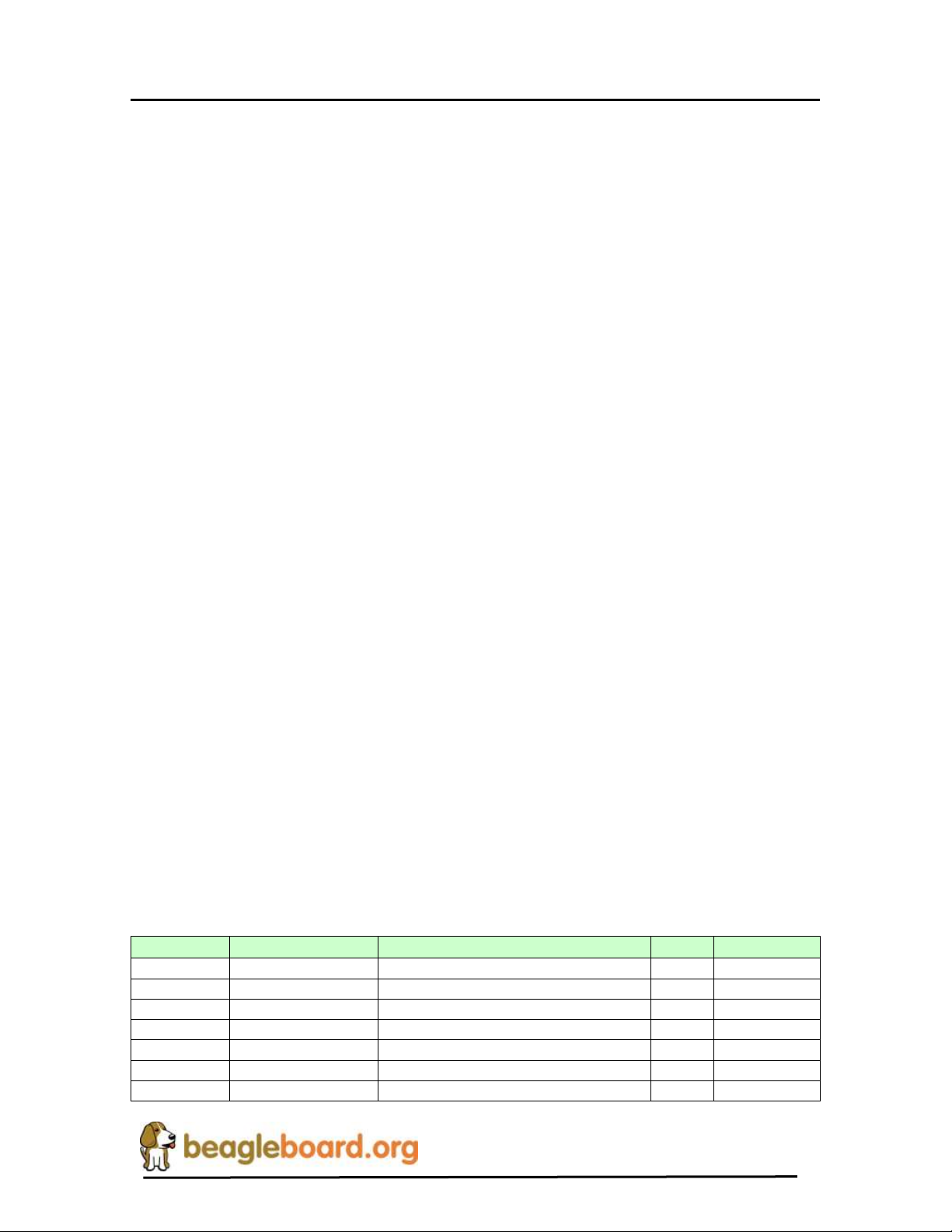
REF: BB_SRM_xM
BeagleBoard-xM System
Reference Manual
Revision C2
Signal
Function
Description
I/O
Processor
cam_hs
HS
Camera Horizontal Synchronization
I/O
A24
cam_vs
VS
Camera Vertical Synchronization
I/O
C25
cam_xclka
Clock
Camera Clock Output
O
cam_d0
Camera Data
Camera image data bit 0
I
AG17
cam_d1
Camera Data
Camera image data bit 1
I
AH17
cam_d2
Camera Data
Camera image data bit 2
I
B24
cam_d3
Camera Data
Camera image data bit 3
I
C24
The 5V is on whenever a power source is applied to the board and cannot be controlled.
This makes the 3.3V rail more suitable as it allows you to totally remove the power form
the camera module.
7.20.1.2 CAM_DIGITAL Power
The digital power is a 1.8V rail that is supplied by the TPS65950. The power is
controlled via the I2C1 interface from the processor by setting the VAUX3 regulator to
1.8V. This is used for the internal logic in the camera module.
7.20.1.3 CAM_IO Power
The I/O power is a 1.8V rail that is supplied by the TPS65950. The power is controlled
via the I2C1 interface from the processor by setting the VAUX4 regulator to 1.8V. This
will set the level of all of the interface signals to the processor. If this rail is set to a
voltage higher than 1.8V, it will damage the processor if the camera module is inserted.
7.20.2 Camera I2C Port
The processor uses the I2C2 port to communicate to the camera module to set the
registers in the device. There are no pullups on the board for the I2C to prevent conflict
with add on boards that do have the pullups. If an add-on board is not used, the SW will
need to enable the internal pullups on the I2C2 signals in order for the interface to work.
7.20.3 Processor Camera Port Interface
Table 19 shows the signals that are the interface between the processor and the camera
modules. The I/O status of each pin is defined from the perspective of the processor.
The cam_wen signal is labeled as CMOS_OE on the schematic. All of the current
camera modules do not use this signal and this signal has no affect on the operation of the
camera modules. It is provided for future use.
Table 19. Camera Interface Signals
Page 98 of 163
Page 99
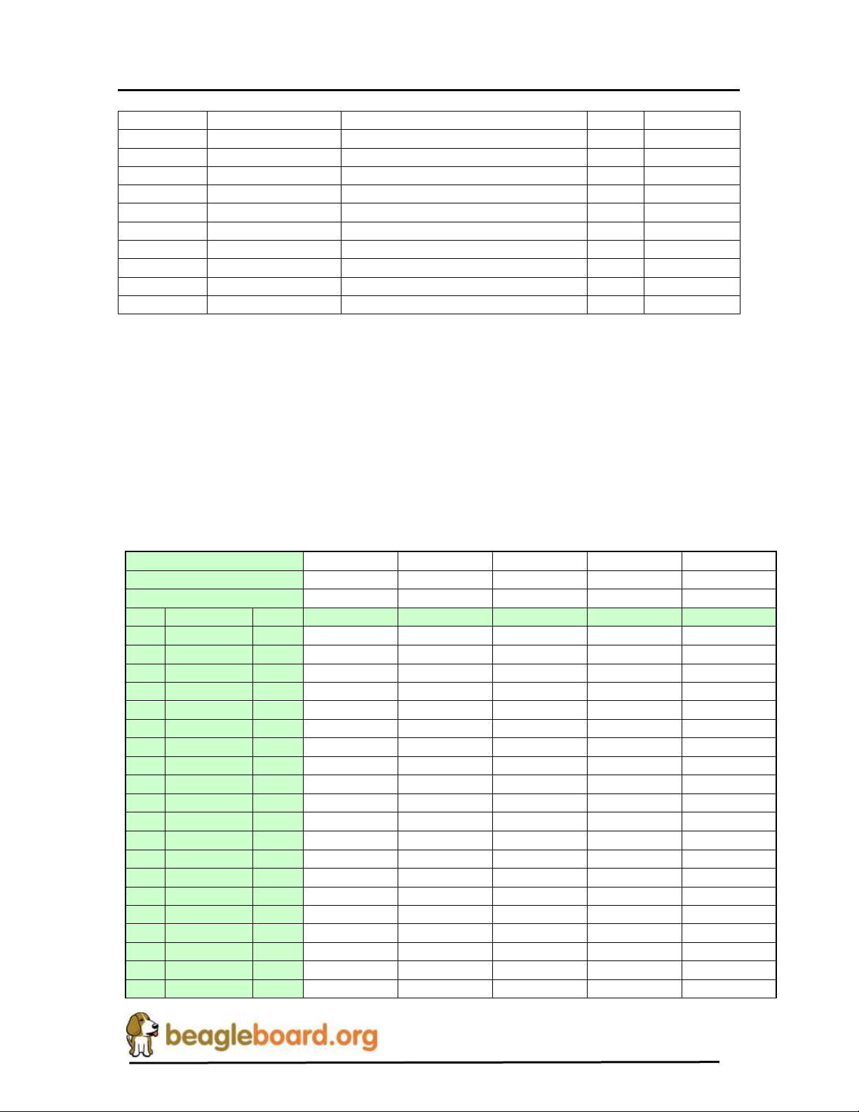
REF: BB_SRM_xM
BeagleBoard-xM System
Reference Manual
Revision C2
cam_d4
Camera Data
Camera image data bit 4
I
D24
cam_d5
Camera Data
Camera image data bit 5
I
A25
cam_d6
Camera Data
Camera image data bit 6
I
K28
cam_d7
Camera Data
Camera image data bit 7
I
L28
cam_d8
Camera Data
Camera image data bit 8
I
K27
cam_d9
Camera Data
Camera image data bit 9
I
L27
cam_d10
Camera Data
Camera image data bit 10
I
B25
cam_d11
Camera Data
Camera image data bit 11
I
C26
cam_fld
RESET
Camera field identification
I/O
C23
cam_pclk
Pixel Clock
Camera pixel clock
I
C27
cam_wen
Camera Write Enable
I
B23
Resolution
VGA
1.3MP
2MP
3MP
5MP
Camera Module Part Number
LI-LBCMVGA
LI-LBCM1M1
LI-LBCM2M1
LI-BCM3M1
LI-LBCM5M1
Data Width--->
10
10
10 8 12
PIN
NAME
I/O/V
1
D11 I D9
D9
D9
D7
D11
2
MCLK
O
MCLK
MCLK
MCLK
MCLK
MCLK
3
D10 I D8
D8
D8
D6
D10
4
GND
PWR
GND
GND
GND
GND
GND
5
D9 I D7
D7
D7
D5
D9
6
SDATA
I/O
SDATA
SDATA
SDATA
SDATA
SDATA
7
D8 I D6
D6
D6
D4
D8 8 SCLK
I/O
SCLK
SCLK
SCLK
SCLK
SCLK
9
D7 I D5
D5
D5
D3
D7
10
RESET
O
RESET
RESET
RESET
RESET
RESET
11
D6 I D4
D4
D4
D2
D6
12
OE O OE
OE
OE
OE
OE
13
D5 I D3
D3
D3
D1
D5
14
GND
PWR
GND
GND
GND
GND
GND
15
D4 I D2
D2
D2
D0
D4
16
CAM_IO
PWR
CAM_IO
CAM_IO
CAM_IO
CAM_IO
CAM_IO
17
D3 I D1
D1
D1
PULL-DOWN
D3
18
CAM_IO
PWR
CAM_IO
CAM_IO
CAM_IO
CAM_IO
CAM_IO
19
D2 I D0
D0
D0
PULL-DOWN
D2
20
GND
PWR
GND
GND
GND
GND
GND
The cam_fld signal is used as a RESET signal to the camera board. When used as a reset,
the pin should be set up as a GPIO pin.
Table 20 shows the mapping of the pins on the camera sensors to the pins on the
processor. In order to work with the different modules, you must take into account the
order of the bits. The table covers the currently available camera modules that are
compatible with the Beagle –xM. You will notice some of the lettering in red. These are
signals that are not used by the camera module. In order for the data to be correct, these
signals need to be tied low by enabling the internal pulldown resistors.
Table 20. Camera Pin Signal Mapping
Page 99 of 163
Page 100
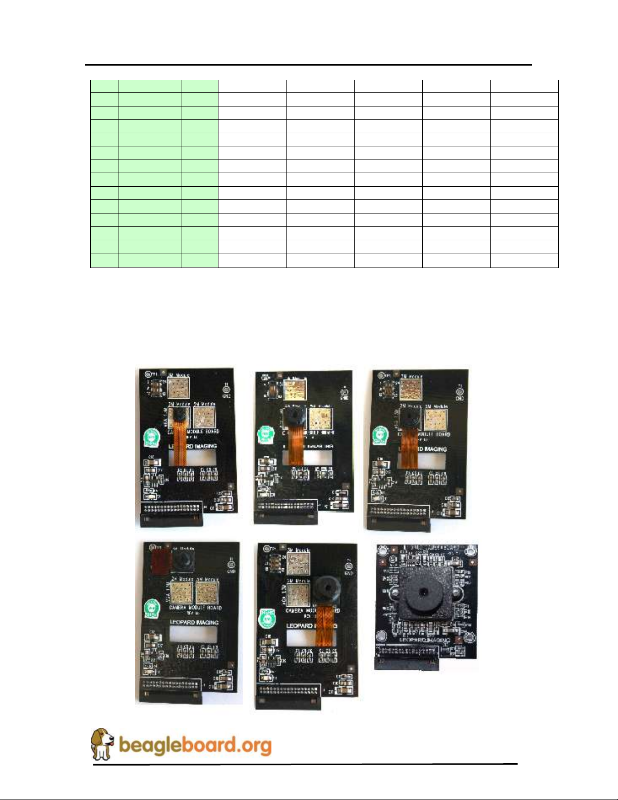
REF: BB_SRM_xM
BeagleBoard-xM System
Reference Manual
Revision C2
21
D1
I
PULL-DOWN
PULL-DOWN
PULL-DOWN
PULL-DOWN
D1
22
GND
PWR
GND
GND
GND
GND
GND
23
D0
I
PULL-DOWN
PULL-DOWN
PULL-DOWN
PULL-DOWN
D0
24
CAM_ANA
PWR
CAM_ANA
CAM_ANA
CAM_ANA
CAM_ANA
CAM_ANA
25
CAM_ANA
PWR
CAM_ANA
CAM_ANA
CAM_ANA
CAM_ANA
CAM_ANA
26
CAM_ANA
PWR
CAM_ANA
CAM_ANA
CAM_ANA
CAM_ANA
CAM_ANA
27
PCLK
I
PCLK
PCLK
PCLK
PCLK
PCLK
28
GND
PWR
GND
GND
GND
GND
GND
29
HS I HS
HS
HS
HS
HS
30
CAM_DIG
PWR
CAM_DIG
CAM_DIG
CAM_DIG
CAM_DIG
CAM_DIG
31
VS I VS
VS
VS
VS
VS
32
CAM_DIG
PWR
CAM_DIG
CAM_DIG
CAM_DIG
CAM_DIG
CAM_DIG
33
GND
PWR
GND
GND
GND
GND
GND
34
GND
PWR
GND
GND
GND
GND
GND
7.20.4 Camera Modules
The camera module can be purchased from Leopard Imaging or one of their distributors.
It uses the same modules as the LeopardBoard DM355 version. The figure below shows
the different modules that can be used. The part numbers can be found in Table 20.
Page 100 of 163
 Loading...