

Page 1
MX57QM
Intel® Core™ i3, i5, i7 Mobile
Socket 989 Arrandale Processors Support
User’s Quick Start Card Ver s io n 1.1 http://www.bcmcom.com
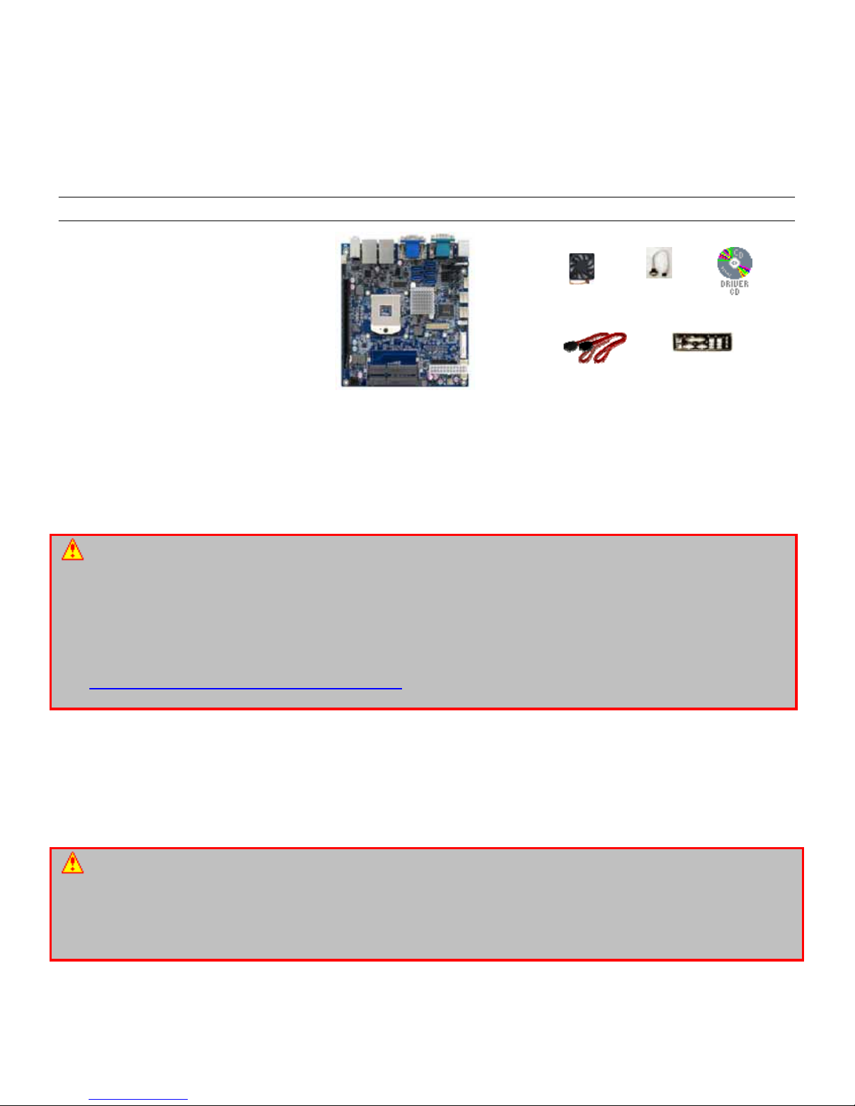
Inspect the Package:
One MX57Q M Motherboard
One Standard I/O Shield
One CPU Cooler
Two COM Port Cables
Two SAT A Cables
One Driver CD
One User’s Q uic k Start Car d
MX57QM
CPU Cooler
Responsibility:
This manual is provided “As-Is” with no warranties of any kind, expressed or implied, including, but not limited to the implied
warranties or conditions of this product’s fitness for any particular purpose. In no event shall we be liable for any loss of
profits, loss of business, loss of data, interruption of business, or indirect, special, incidental, or consequential damages of
any kind, e ven t he possibilit y of s uch d ama ges arising from a ny defe ct or er ror in t his ma nual or prod uct . We reserve t he
right to modify and update the user manual without prior notice.
COM Port
Cables
I/O Shield
WARNING: CMOS Battery Damage
Replace your system ’s CMOS RAM battery only with the identical CR-2032 3V L ithium-Ion coin cell (or e quivalent) battery
type to avoid risk of personal injury or physical damage to your equipment. Improper installation might cause battery to
explode. Always dispose of used batteries according to the manufacturer’s instructions, or as required by the local
ordinance (where applicable). T he dama ge due t o not followi ng thi s warni ng will vo id your motherboard’ s m anufacturer
warranty.
Perchlorate Material- Special Handling May Apply.
See http://www.dtsc.ca.gov/hazardouswaste/perchlorate/
Additional Information:
Additio nal inform ati o n o n s ett i ng this bo ard up can be f ound i n t he U s er ’s M anual in t he provided CD or DV D R OM. The
Online User’s Manual and FAQ/Knowledge Base can be found on our website by visiting our website:
http://www.bcmcom.com. If your question is not answered in our FAQ/Knowledge Base, visit our forums and post your
messages or submit a new FAQ through FAQ Submittal form for us to add your question in our FAQ with our answer.
ATTENTION: Incorrect BIOS Setup
If you do not know how to handle BIOS setup or how to set it up properly, it is strongly advisable that you do not modify any
of the se tti ng s than otherwis e i ns tr ucted i n t he User’s Quic k S tart Ca rd. Even a s eemingl y sm all inc orr e ct a djustme nt or
modificat ion in t he BIOS setup ca n render y our system unsta ble or u nusabl e. Incorr ect B IOS setup is not c over ed by your
motherboard’s manufacturer warranty. Try Clear CMOS information when system does not boot after BIOS settings
change.
1
Page 2
WARNING: Electr ostat ic Sensitive Device (ESD)
Static el ectric ity ca n easily damage your mother board a nd will void your motherbo ard warr ant y. Keep the mo therbo ard
and other s yst em com po nents in their anti-static packaging unti l you are re ady to install them . Touch a ground e d surf ace
befo r e you remove any system component from its protective anti-static packaging. Unpacking and installation should be
done on a grounded, anti- static mat. The operator should be wearing a n anti-stat ic wristband, grounded at the sam e
points as the anti- st atic m at. During co nfig urat ion and i nstall atio n t ouch a gr o unded sur face f req uentl y to d isc harge any
static electrical charge that may have built up in your body. Avoid touching the components when handling the
motherboard or a peripheral card. Handle the motherboard and periph eral cards either by the edges or by the peripheral
card case-mounting bracket.
WARNING: Mi spl aced Jumper Damage
Incorrect jumper s and connectors settings may lead to damage to your motherboard and will void your motherboard
warranty. Please pay special attention to not connect these headers in the wrong direction. DO NOT change ANY jumpers
while the motherboard has power.
Jumpers
Label Function
PCIE_JP1 Mini PCIE Rev1.1 & 1.2 Mode Selection
COMS1 Clear CMOS Selection
JP2 Backlight Enable Selection
JP3 Backlight Power Selection
JP5 Power Mode Selection
JP6 COM3 Signal / Power Selection
JP7 COM1 Signal / Power Selection
JP8 COM2 Signal / Power Selection
JP9 COM6 Signal / Power Selection
JP10 COM4 Signal / Power Selection
JP11 COM5 Signal / Power Selection
2
Page 3
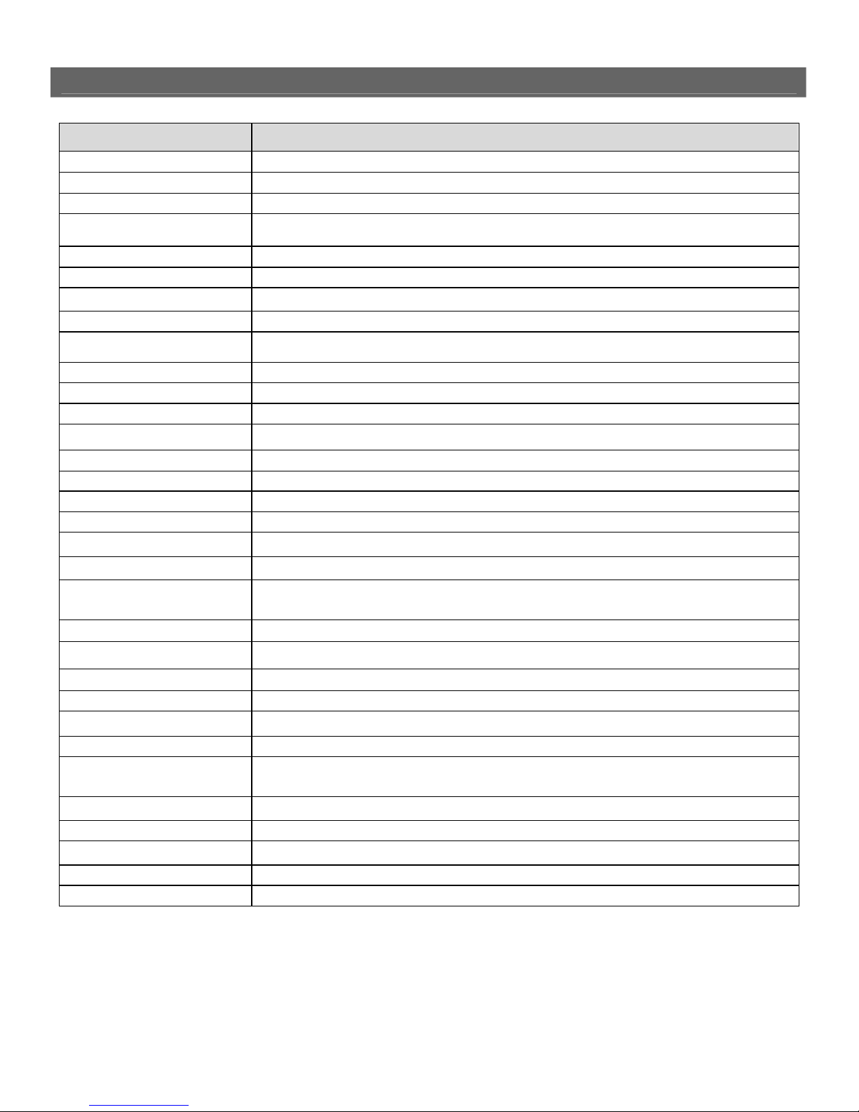
Connectors & Headers
Label Function
DIMM1 DDR3 Memory SO-DIMM Socket
DIMM2 DDR3 Memory SO-DIMM Socket
CPU_FAN1 CPU FAN Wafer
CHA_FAN1 SYSTEM FAN Wafer
MPCIE1 PCIE x 1 Slot
IR1 IrDA Pin Header
LVDS1 LVDS Panel Pin Header
BL1 Panel Backlight Wafer
ATXPWR1 24-pin ATX Power Input Connector
CN1 Debug port Connector
COM2 RS-232 Port 2 Box Header
COM3 RS-232 Port 3 Box Header
COM4 RS-232 Port 4 Box Header
COM5 RS-232 Port 5 Box Header
COM6 RS-232 Port 6 Box Header
SATA1 S erial ATA Connect or
SATA2 S erial ATA Connect or
SATA3 S erial ATA Connect or
SATA4 S erial ATA Connect or
SATA5
USB1 USB2.0 Port 4, 5 Pin Header
USB2 USB2.0 Port 8, 9 Pin Header
AMP_L1 Left Channel 2W Audio AMP Output Wafer
AMP_R1 Right Channel 2W Audio AMP Output Wafer
PCIE1 PCIExpress X16 Slot
SPDIF1 S/PDIF Pin Header
DIO1
BZ1 Buzzer
FP1 Front Panel 1 Pin Header
FP2 Front Panel 2 Pin Header
FP3 Front Panel Audio Pin Header
CF1 CF socket
Serial ATA Connector
(The fifth SATA connector signals share with Mini-PCIe slot,)
16-bits DIO Connector
(8-bits Input and 8-bits Output)
3
Page 4
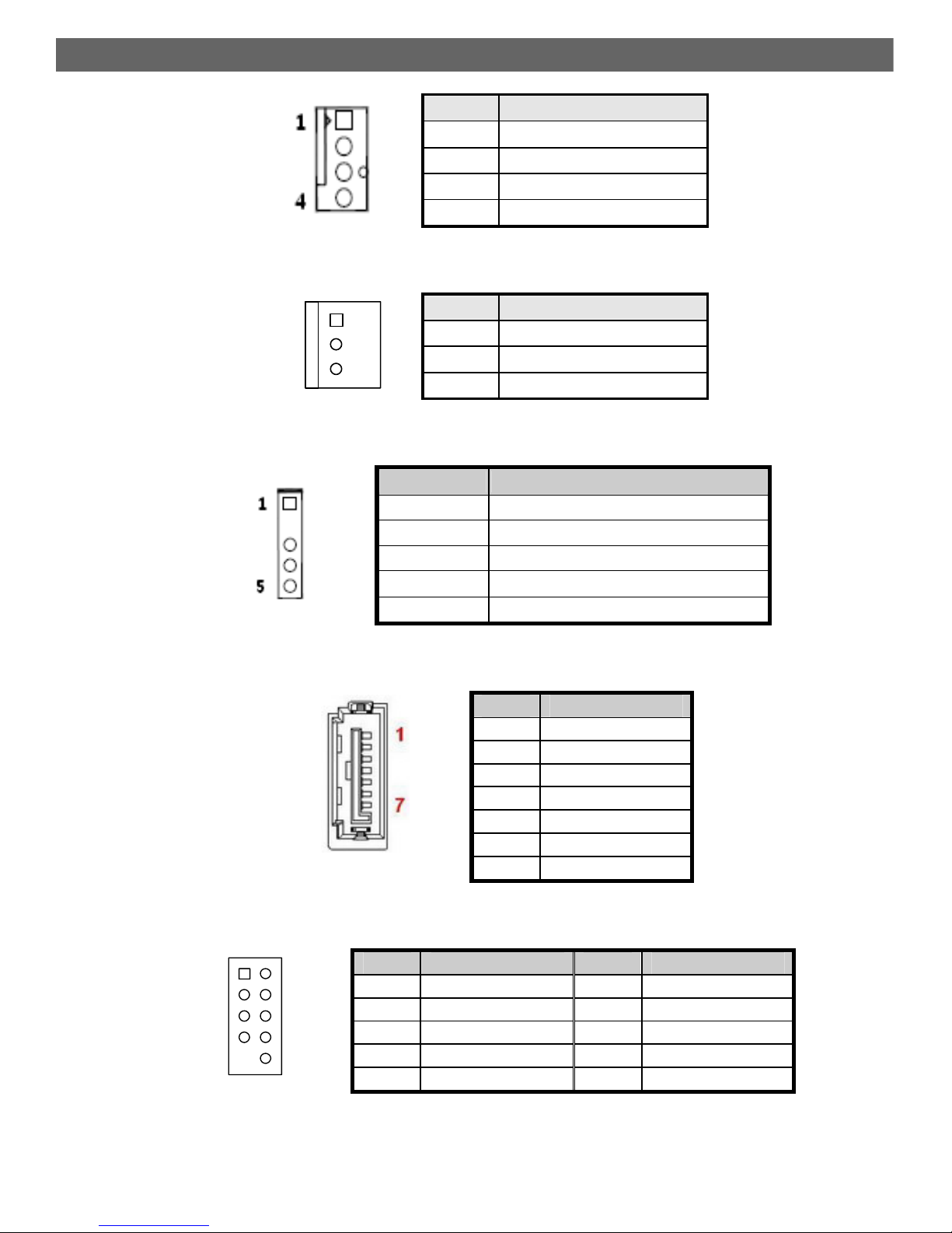
Internal Connector Pin Assignment
CPU_FAN1 CPU FAN Wafer
Pin Signal
1 GND
2 +12V
3 FAN_CPU_TACH
CHA_FAN1 SYSTEM FAN Wafer
1
2
3
IR1 IrDA remote contro l Wafer
Pitch:2.54mm
SATA1, SATA2, SATA3, SATA4, SATA5 Serial ATA Connector
USB1,USB2 USB Pin Header
1
3
5
2
4
6
87
10
Pin Signal Name Pin Signal Name
1 +5V 2 +5V
3 USB2- 4 USB35 USB2+ 6 USB3+
7 GND 8 GND
9 KEY 10 GND
Pitch:2.54mm
4 FAN_CPU_CTRL
Pitch: 2.54mm WAFER
Pin Signal
1 GND
2 +12V
3 HW_FANIN1
Pitch: 2.54mm WAFER
Pin Signal Name
1 +5v
2 NC
3 IRRX
4 GND
5 IRTX
Pin Signal Name
1 GND
2 TX+
3 TX4 GND
5 RX6 RX+
7 GND
4
Page 5
R
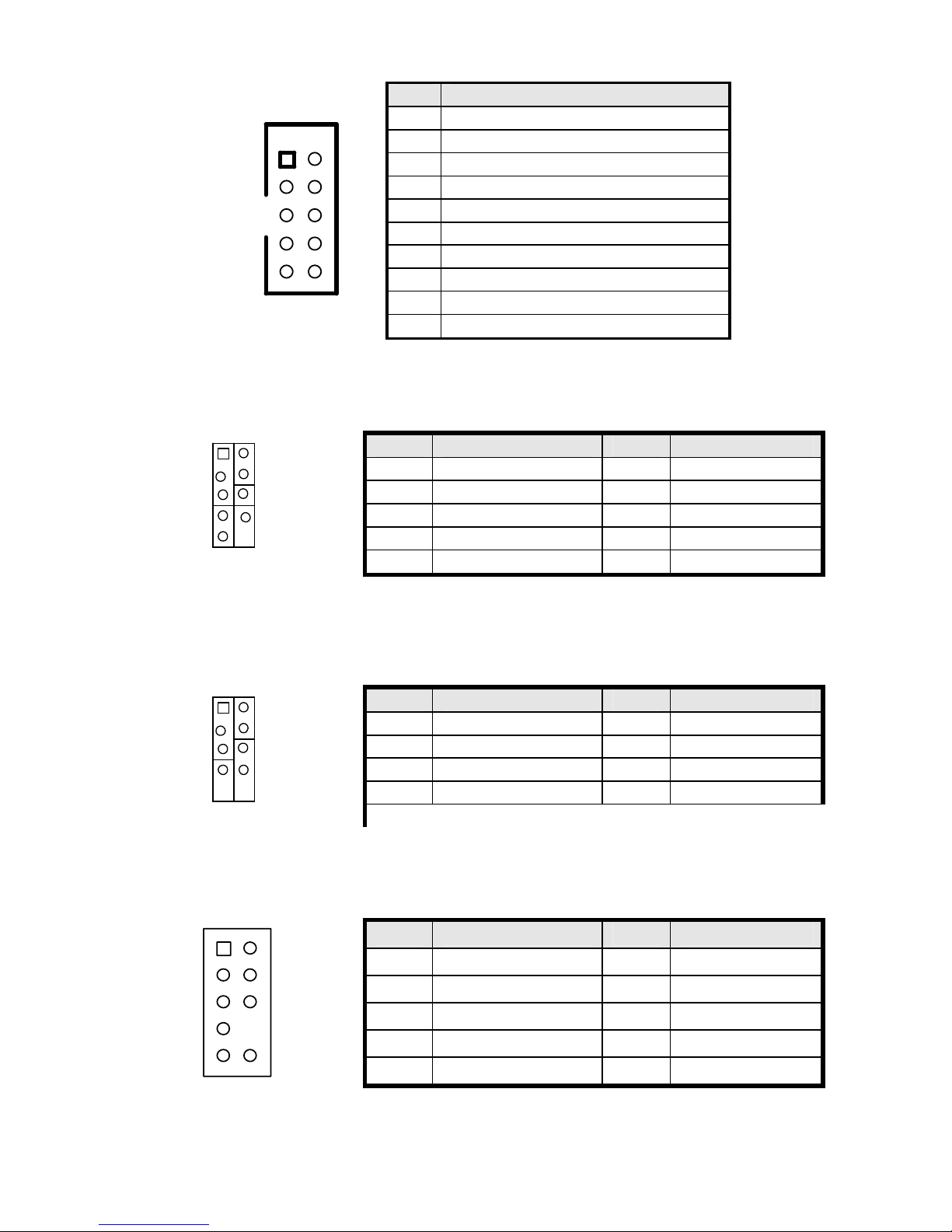
COM2,COM3,COM4,COM5,COM6 RS-232 Box Header
Pin Signa l
1 DCD, Da t a c ar r i er d et e ct
2 RXD, Rec ei ve dat a
1
3
5
7
2
4
6
8
3 TXD, Transmit data
4 DTR, Data terminal ready
5 GND, ground
6 DSR, Data set ready
7 RTS, Request to send
9
10
8 CTS, Clear to send
9 RI, Ring indicator
10 NC
Pitch:2.0mm WAFER
FP1 Front Panel 1 Pin Header
+ 2
HLED
-
RESET
9 10
+1
PLED
+
PW
-
FP2 Front Panel 2 Pin Header
KLOCK
SMD
SMC -
+
+
7
2
8
+1
SPKR
-
Pin Signal Pin Signal
1 HDD LED + 2 Power LED +
3 HDD LED - 4 Power LED 5 Reset Button + 6 Power Button +
7 Reset Button - 8 Power Button 9 10 [KEY]
Pitch:2.54mm
Pin Signal Pin Signal
1 Keyboard Lock 2 Speaker +
3 GND 4 NC5 SMBus Data 6 NC
7 SMBus Clock 8 Speaker +
FP3 Digital Input / Output Pin Header
1
9
2
10
Pitch:2.54mm
Pin Signal Pin Signal
1 MIC_L 2 GND
3 MIC_R 4 ACZ_DET#
5 LIN_R 6 MIC_JD
7 SENSE 8 NC
9 LIN_L 10 LINE_JD
Pitch:2.54mm
5
Page 6
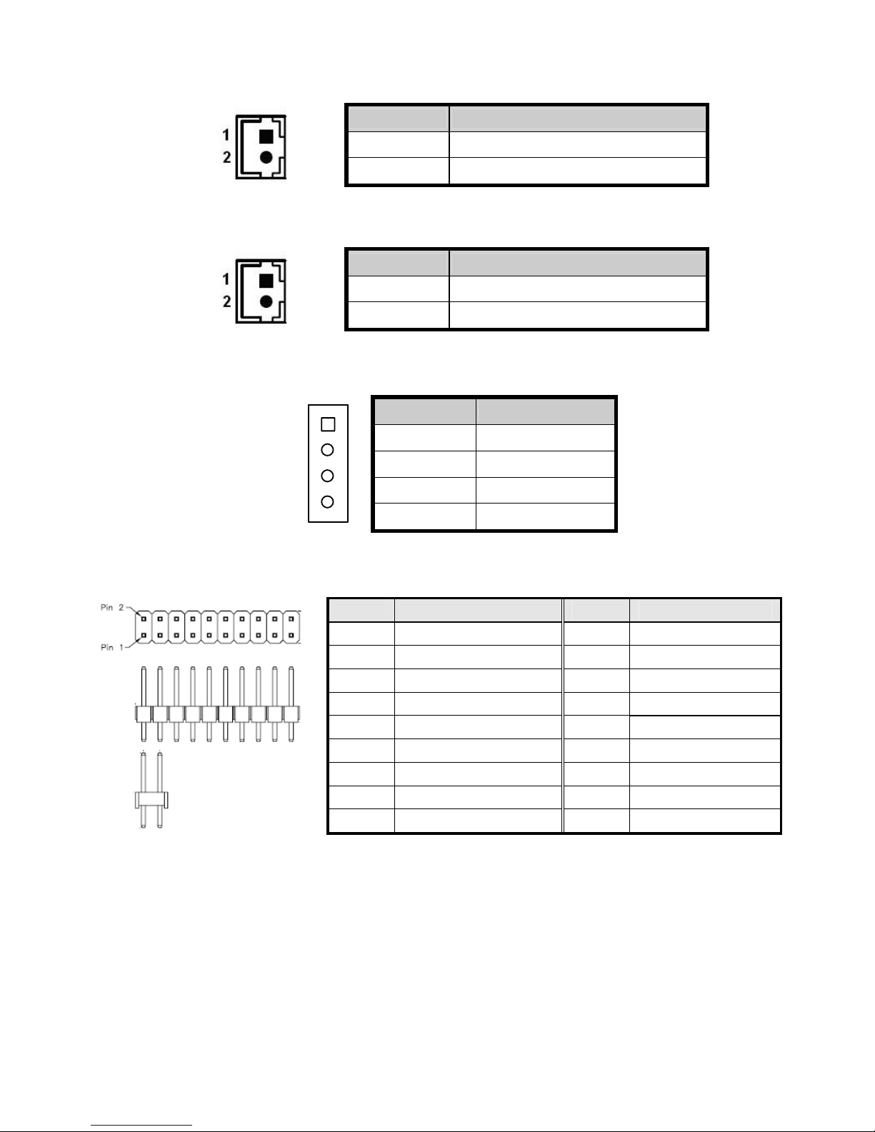
AMP_R1 Audio AMP Right Output Wafer
Pin Signal Name
1 Speaker+
AMP_L1 Audio AMP Left Output Wafer
2 Speaker-
Pitch:2.0mm WAFER
Pin Signal Name
1 Speaker+
2 Speaker-
Pitch:2.0mm WAFER
SPDIF1 S/PDIF Pin Header
Pin Signal Name
1
4
Pitch:2.54mm
1 S/PDIF In
2 GND
3 S/PDIF Out
4 GND
DIO1 Digital Input / Digital Output Pin Header
Pin Signal Pin Signal
1 +5V 2 GND
3 DO0 4 DI0
5 DO1 6 DI1
7 DO2 8 DI2
9 DO3 10 DI3
11 DO4 12 DI4
13 DO5 14 DI5
15 DO6 16 DI6
17 DO7 18 DI7
DIP 18P 2R MALE STRAIGHT TYPE Pitch:2.54mm
6
Page 7
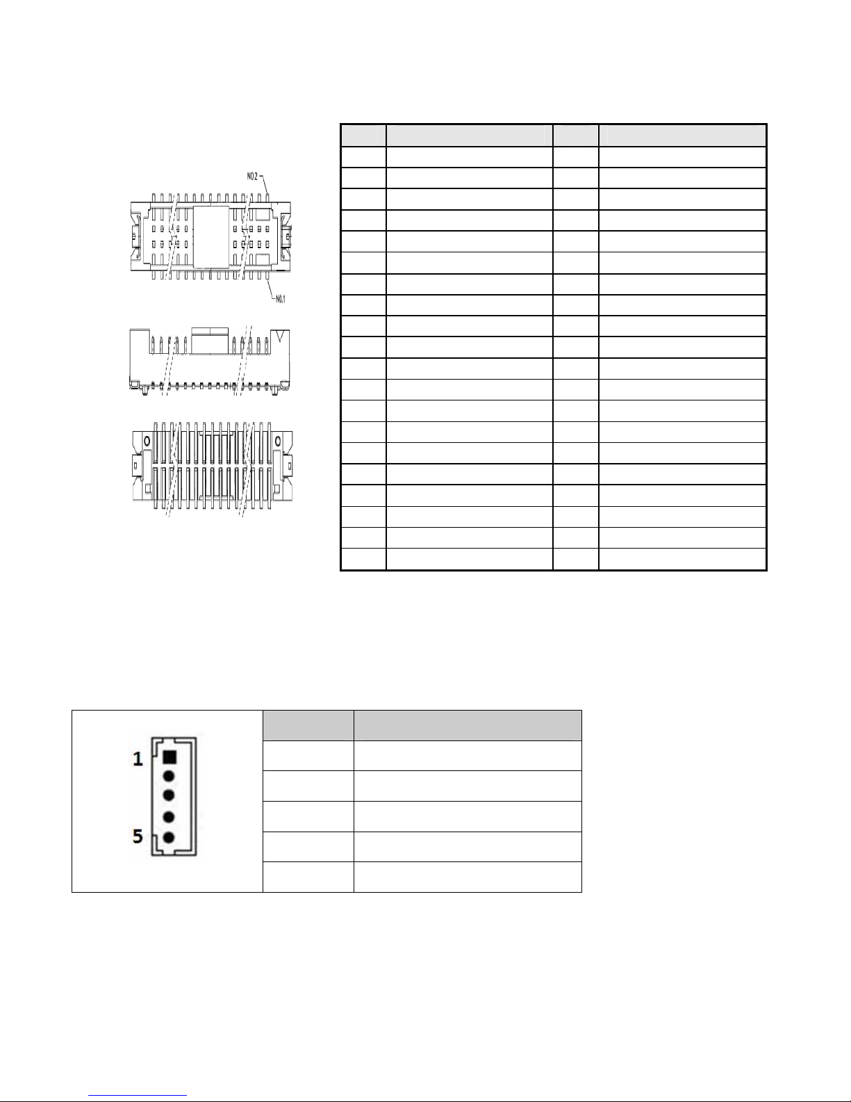
LVDS1 Channel 1 LVDS Connector
Pin Signal Name Pin Signal Name
Pitch:1.25mm
1 +3.3V 2 +5V
3 +3.3V 4 +5V
5 DDC_CLK 6 DDC_DATA
7 GND 8 GND
9 LVDS0_DATA1 10 LVDS0_DATA0
11 LVDS0_DATA#1 12 LVDS0_DATA#0
13 GND 14 GND
15 LVDS0_DATA3 16 LVDS0_DATA2
17 LVDS0_DATA#3 18 LVDS0_DATA#2
19 GND 20 GND
21 LVDS1_DATA1 22 LVDS1_DATA0
23 LVDS1_DATA#1 24 LVDS1_DATA#0
25 GND 26 GND
27 LVDS1_DATA3 28 LVDS1_DATA2
29 LVDS1_DATA#3 30 LVDS1_DATA#2
31 GND 32 GND
33 LVDS1_CLK 34 LVDS0_CLK
35 LVDS1_CLK# 36 LVDS0_CLK#
37 GND 38 GND
39 +12V 40 +12V
BL1 LVDS Backlight Inverter Wafer
Pin Signal Name
1 Backlight Control
2 GND
3 Backlight Power
4 Backlight Power
5 Backlight Enable
Pitch:2.0mm
7
Page 8
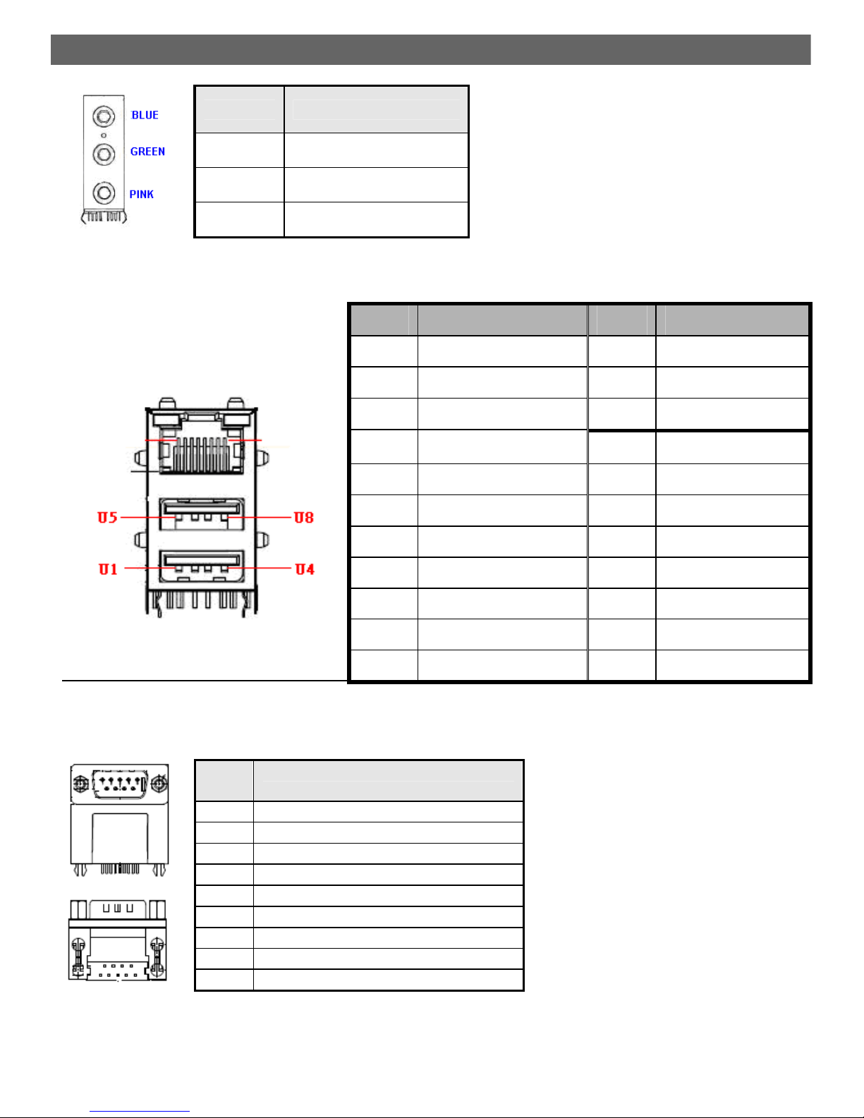
Rear Panel Connector List
AUDIO1 Audio Phone Jack
Signal Name
BLUE LINE IN
GREEN LINE OUT
PINK MIC IN
AUDIO JACK*3 DIP Vertical
LAN1, LAN2 RJ-45 + USB Port-0&1 Connector
Pin Signal Pin Signal
1 VCC 12 Yellow LED
2 D0+ 13 Green LED#
3 D0- 14 Orange LED#
4 D1+ U1 USB_PWR
5 D1- U2 USB_N0
6 D2+ U3 USB_P0
7 D2- U4 GND
8 D3+ U5 USB_PWR
9 D3- U6 USB_N1
COM1 RS-232 DB-9 Connector
Pin
1 DCD, Data carrier detect
2 RXD, Receive data
3 TXD, Transmit data
4 DTR, Data terminal ready
5 GND, ground
6 DSR, Data set ready
7 RTS, Request to send
8 CTS, Clear to send
9 RI, Ring indicator
D-SUB 9P 90D (M)
10 GND U7 USB_P1
11 Yellow LED# U8 GND
USB*2/RJ45*1+TFM+LED(10/100/ 1000)22P DIP 90°
Signal
8
Page 9
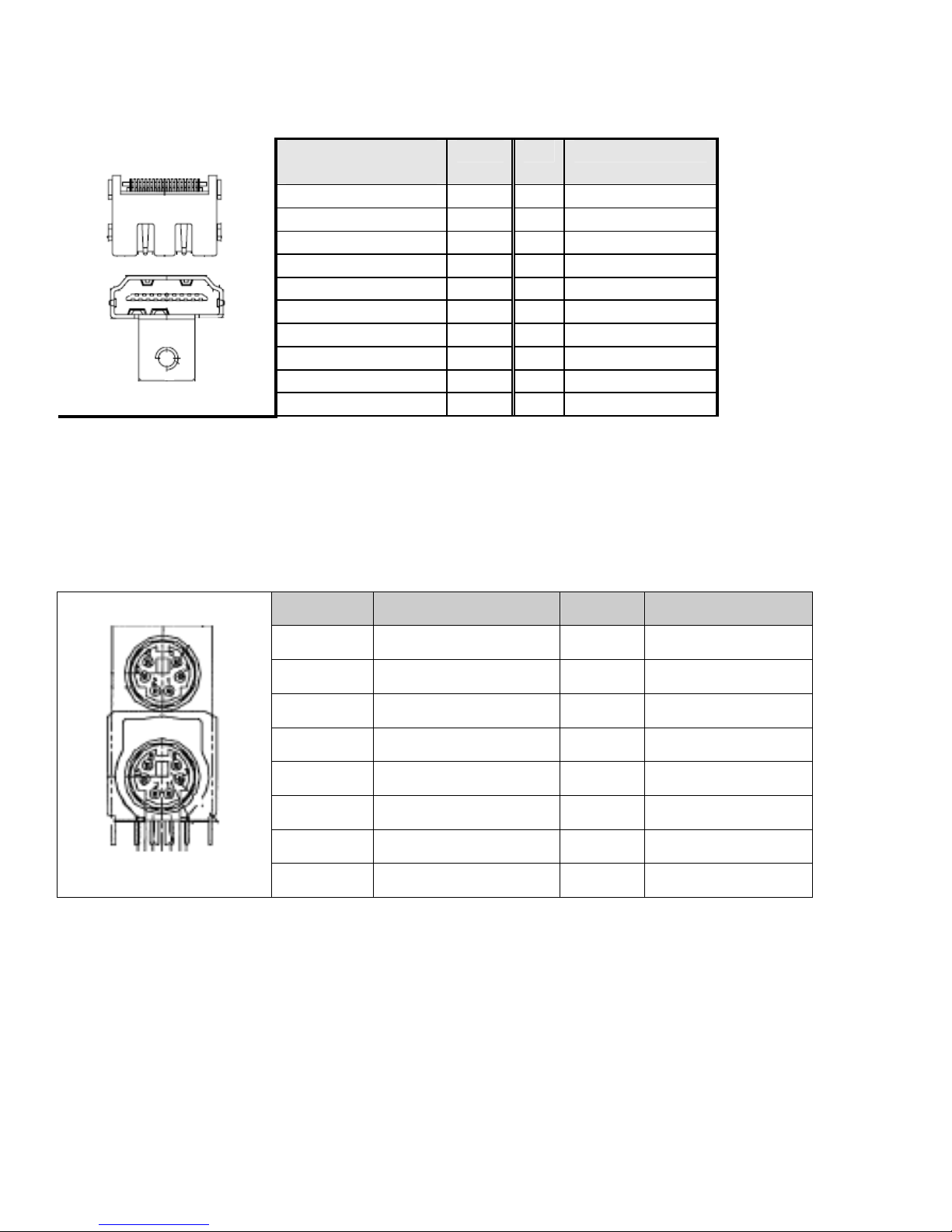
Hdmi1 Connector
PS-KBMS1 Internal PS/2 Keyboard & Mouse
Signal Name
TMD_DATA2+ 1 2 GND
TMD_DATA2- 3 4 TMD_DATA1+
GND 5 6 TMD_DATA1-
TMD_DATA0+ 7 8 GND
TMD_DATA0- 9 10 HDMI_TCLP
GND 11 12 HDMI_TCLN
NC 13 14 NC
DDC_CLK 15 16 DDC_DATA
GND 17 18 +5V
HPDET 19
HDMI right angle
Pin Signal Name Pin Signal Name
Pin Pin Signal Name
1 KB_DATA 2 NC
3 GND 4 KB_PWR
5 KB_CLK 6 NC
7 MS_DATA 8 NC
9 GND 10 KB_PWR
11 MS_CLK 12 NC
13 GND 14 GND
15 GND 16 GND
DIP 6/6P MH11061-P36-4F 90D(F) Kb/Ms
9
Page 10
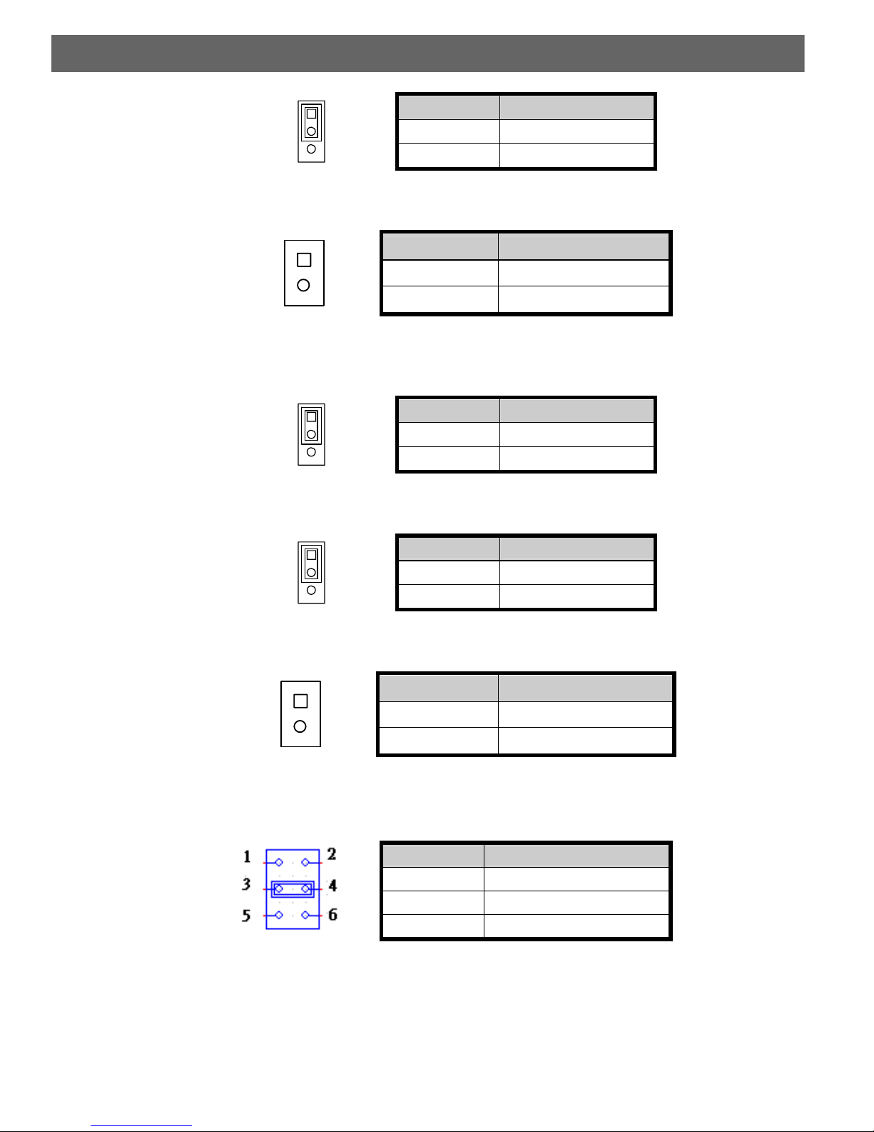
Jumper Settings
PCIE_JP1 Mini PCIE Version Selection
1
2
3
COMS1 Clear CMOS Selection
1
2
JP2 Backlight Enable Selection
1
2
3
JP3 Backlight Power Selection
Jumper Status
1-2 (Default) MPCIE Rev1.1
2-3 MPCIE Rev1.2
Pitch: 2.0mm
Jumper Status
pen (Default) Normal Operation
Short Clear CMOS
Pitch: 2.54mm
Jumper Status
1-2 (Default) High Active
2-3 Low Active
Pitch: 2.0mm
1
2
3
Jumper Status
1-2 (Default) +12V
2-3 +5V
Pitch: 2.0mm
JP5 Power mode Selection
Jumper Status
1
2
Open (Default) ATX Mode
Short AT Mode
Pitch: 2.54mm
JP6 –JP11 COM1-6 Signal / Power Selection
Jumper Status
1-2 Pin 9 of COM3 = +12V
-4 (Default) Pin 9 of COM3 = RI
5-6 Pin 9 of COM3 = +5V
Pitch: 2.0mm
10
Page 11
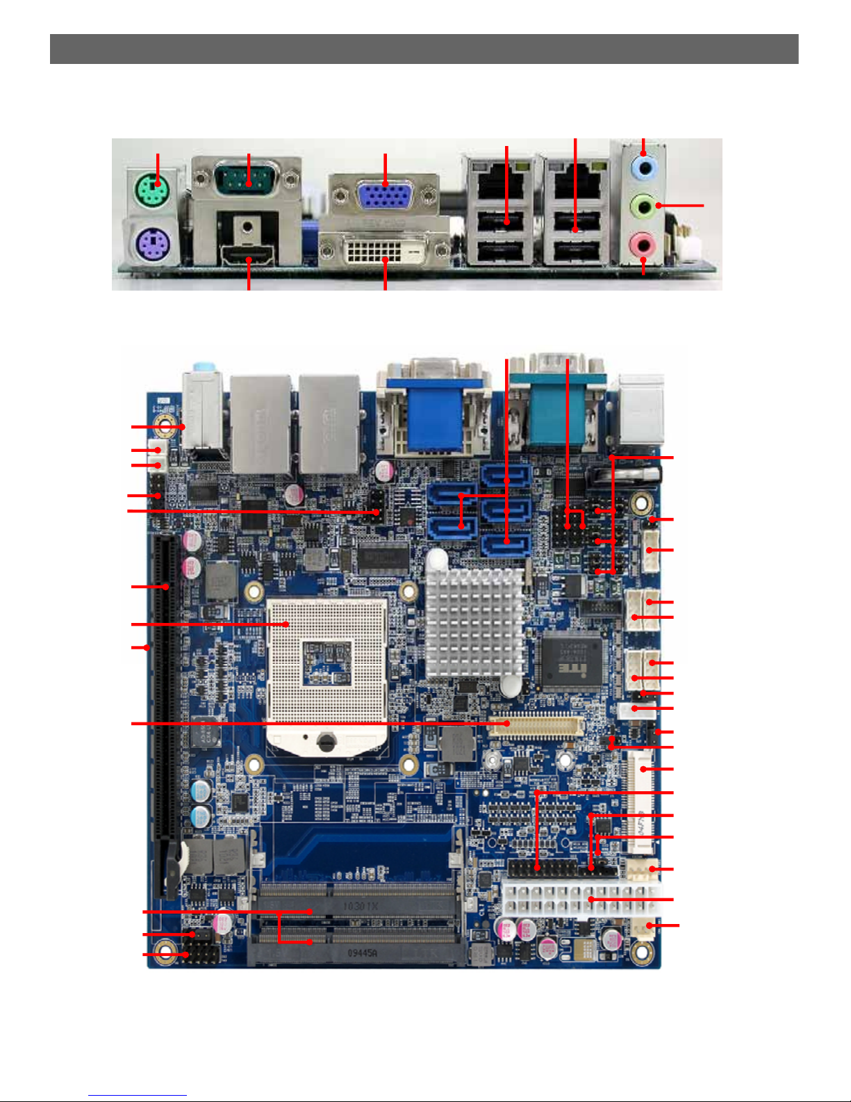
Motherboard Layout:
PS2 KB/MS
SPDIF1
AMP_R1
AMP_L1
FP3
SPI_CN1
PCIE1
CPU SOCKET
CF1
(BOTTOM SID E)
JLVDS1
SODIMM1, 2
FP2
FP1
COM1
HDMI
VGA
DVI
LAN_USB1
SATA1-5
LAN_USB2
LINE-IN
LINE-OUT
MIC
USB1, 2
J8, J7
J6, 10
J11, J9
COMS1
COM 2
COM 3
COM 4
COM 5
COM 6
JP2
JBKL1
JP3
JP5
MPCIE X1
DIO1
IR1
PCIE_JP1
CPU_ FAN1
ATX
CHA_ FAN1
11
Page 12
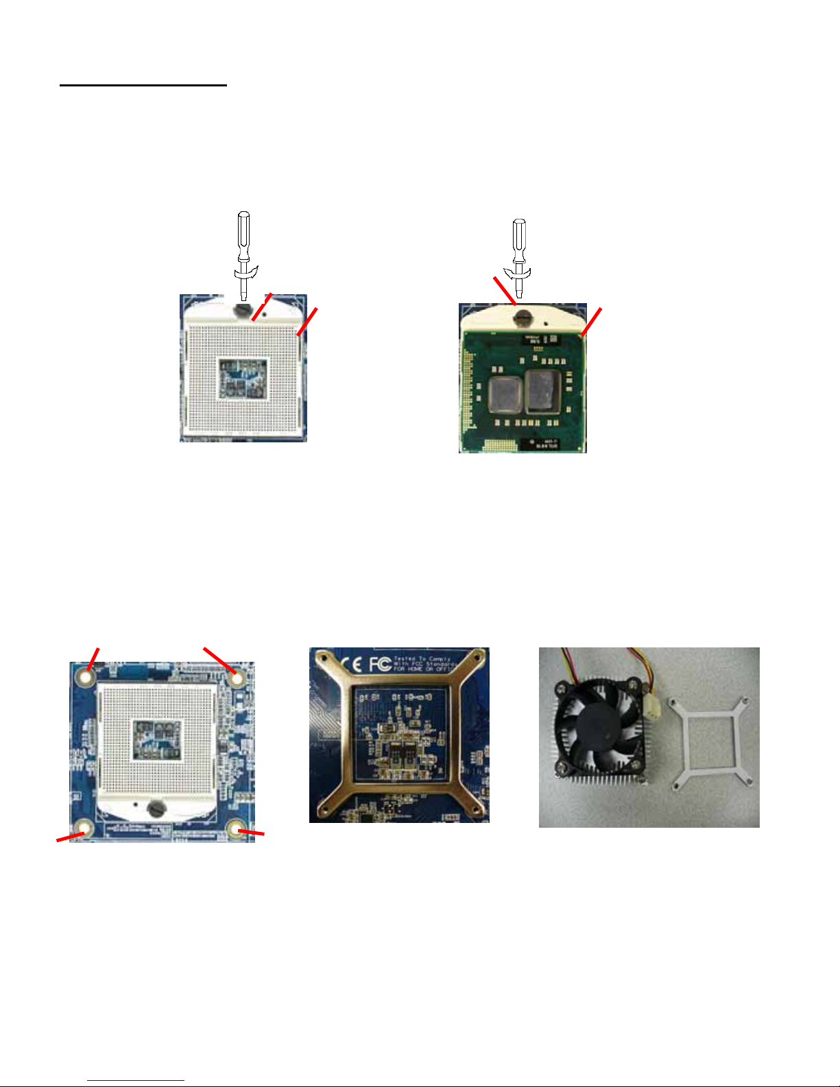
CPU Installation
This processor is intended to be pr ofessionally installe d. T ake proper electrostatic s discharge (ESD)
precautions such a s using approp riate ground strips, gloves, an d ESD mats.
• Insert CPU into CPU socket and turn the screw to the lock position.
Note: Do not force the CPU into the socket. It may bend the pins and damage the CPU.
Installing t he CP U Coole r
z -Insert the retention bracket through the screw hole from bottom sid e of motherboar d.
-Match and place CPU cooler assembly on the top of CPU and retention bracket.
-Tighten the screws into the retention bracket.
Screw holes Retention bracket CPU cooler & Retention bracket
(rear side)
Note: Make sure CPU cooler assembly and CPU top surface are in total contact to avoid CPU
overheating problem which would cause the system to hang or unstable.
Unlock
Pin 1 of the
socket
Lock
Gold triangular
mark
12
 Loading...