

Page 1
User’s Manual
MX255D
3rd Generation Intel® Atom™ D2550 Fanless Mini
ITX Motherboard (Cedar Trail Platform) supports 12V
DC Power
Page 2

ii
▍ Preface
Copyright NoticeCopyright Notice
The material in this document is our intellectual property. We take every
care in the preparation of this document, but no guarantee is given as to the
correctness of its contents. Our products are under continual improvement
and we reserve the right to make changes without notice.
TrademarksTrademarks
All trademarks are the properties of their respective owners.
■ NVIDIA
®
is registered trademark of NVIDIA Corporation.
■
ATI® is registered trademark of ATI Technologies, Inc.
■
AMD® is registered trademarks of AMD Corporation.
■
Intel® is registered trademarks of Intel Corporation.
■
Windows® is registered trademarks of Microsoft Corporation.
■
AMI® is registered trademark of Advanced Micro Devices, Inc.
■
Award® is a registered trademark of Phoenix Technologies Ltd.
■
Realtek® is registered trademark of Realtek Semiconductor Corporation.
Revision HistoryRevision History
Revision Revision Revision HistoryRevision History DateDate
1.1 Production release 08/31/2012
1.2 Update operating temperature 10/16/2012
Page 3

iii
MX255D
Safety Instructions
Safety Instructions
■ Always read the safety instructions carefully.
■ Keep this User’s Manual for future reference.
■ Keep this equipment away from humidity.
■ Lay this equipment on a reliable fl at surface before setting it up.
■ The openings on the enclosure are for air convection hence protects the
equipment from overheating. DO NOT COVER THE OPENINGS.
■ Make sure the voltage of the power source and adjust properly 110/220V
before connecting the equipment to the power inlet.
■ Place the power cord such a way that people can not step on it. Do not
place anything over the power cord.
■ Always Unplug the Power Cord before inserting any add-on card or mod-
ule.
■ All cautions and warnings on the equipment should be noted.
■ Never pour any liquid into the opening that could damage or cause electri-
cal shock.
■ If any of the following situations arises, get the equipment checked by ser-
vice personnel:
◯ The power cord or plug is damaged.
◯ Liquid has penetrated into the equipment.
◯ The equipment has been exposed to moisture.
◯ The equipment does not work well or you can not get it work according
to User’s Manual.
◯ The equipment has dropped and damaged.
◯ The equipment has obvious sign of breakage.
■ DO NOT LEAVE THIS EQUIPMENT IN AN ENVIRONMENT UNCONDI-
TIONED, STORAGE TEMPERATURE ABOVE 60oC (140oF), IT MAY DAMAGE THE EQUIPMENT.
CAUTION
CAUTION: Danger of explosion if battery is incorrectly replaced. Replace only with
the same or equivalent type recommended by the manufacturer.
警告使用者:
這是甲類資訊產品,在居住的環境中使用時,可能會造成無線電干擾,在這種情
況下,使用者會被要求採取某些適當的對策。
廢電池請回收
For better environmental protection, waste batteries should be
collected separately for recycling or special disposal.
Page 4

iv
▍ Preface
CE Conformity
CE Conformity
Hereby, we declare that this device is in compliance with the
essential safety requirements and other relevant provisions set
out in the European Directive.
FCC-B Radio Frequency Interference
FCC-B Radio Frequency Interference
Statement
Statement
This equipment has been tested and found to comply with the
limits for a Class B digital device, pursuant to Part 15 of the
FCC Rules. These limits are designed to provide reasonable
protection against harmful interference in a residential installation. This equipment generates, uses and can radiate radio frequency energy and, if not installed and used in accordance with the instruction manual, may cause harmful
interference to radio communications. However, there is no guarantee that interference will not occur in a particular installation. If this equipment does cause
harmful interference to radio or television reception, which can be determined
by turning the equipment off and on, the user is encouraged to try to correct the
interference by one or more of the measures listed below:
■ Reorient or relocate the receiving antenna.
■ Increase the separation between the equipment and receiver.
■ Connect the equipment into an outlet on a circuit diff erent from that to
which the receiver is connected.
■ Consult the dealer or an experienced radio/television technician for help.
NOTICE 1
NOTICE 1
The changes or modifi cations not expressly approved by the party responsible
for compliance could void the user’s authority to operate the equipment.
NOTICE 2
NOTICE 2
Shielded interface cables and AC power cord, if any, must be used in order to
comply with the emission limits.
VOIR LA NOTICE D’INSTALLATION AVANT DE RACCORDER AU RESEAU.
This device complies with Part 15 of the FCC Rules. Operation is subject to the
following two conditions:
1. this device may not cause harmful interference, and
2. this device must accept any interference received, including interference
that may cause undesired operation.
Page 5

v
MX255D
WEEE Statement
WEEE Statement
ENGLISH
Under the European Union (“EU”) Directive on Waste Electrical and Electronic Equipment,
Directive 2002/96/EC, which takes effect on August 13, 2005, products of “electrical and
electronic equipment” cannot be discarded as municipal waste anymore and manufacturers of covered electronic equipment will be obligated to take back such products at the
end of their useful life.
DEUTSCH
Gemäß der Richtlinie 2002/96/EG über Elektro- und Elektronik-Altgeräte dürfen Elektround Elektronik-Altgeräte nicht mehr als kommunale Abfälle entsorgt werden. Wir haben
europaweit verschiedene Sammel- und Recyclingunternehmen beauftragt, die in die Europäische Union in Verkehr gebrachten Produkte, am Ende seines Lebenszyklus zurückzunehmen. Bitte entsorgen Sie dieses Produkt zum gegebenen Zeitpunkt ausschliesslich
an einer lokalen Altgerätesammelstelle in Ihrer Nähe.
FRANÇAIS
Au sujet de la directive européenne (EU) relative aux déchets des équipement électriques
et électroniques, directive 2002/96/EC, prenant effet le 13 août 2005, que les produits électriques et électroniques ne peuvent être déposés dans les décharges ou tout simplement
mis à la poubelle. Les fabricants de ces équipements seront obligés de récupérer certains
produits en fi n de vie. Par conséquent vous pouvez retourner localement ces matériels
dans les points de collecte.
РУССКИЙ
В соответствии с директивой Европейского Союза (ЕС) по предотвращению
загрязнения окружающей среды использованным электрическим и электронным
оборудованием (директива WEEE 2002/96/EC), вступающей в силу 13 августа 2005
года, изделия, относящиеся к электрическому и электронному оборудованию, не могут
рассматриваться как бытовой мусор, поэтому производители вышеперечисленного
электронного оборудования обязаны принимать его для переработки по окончании
срока службы.
ESPAÑOL
Bajo la directiva 2002/96/EC de la Unión Europea en materia de desechos y/o equipos
electrónicos, con fecha de rigor desde el 13 de agosto de 2005, los productos clasifi cados
como “eléctricos y equipos electrónicos” no pueden ser depositados en los contenedores
habituales de su municipio, los fabricantes de equipos electrónicos, están obligados a
hacerse cargo de dichos productos al termino de su período de vida.
NEDERLANDS
De richtlijn van de Europese Unie (EU) met betrekking tot Vervuiling van Electrische en
Electronische producten (2002/96/EC), die op 13 Augustus 2005 in zal gaan kunnen niet
Page 6

vi
▍ Preface
meer beschouwd worden als vervuiling. Fabrikanten van dit soort producten worden
verplicht om producten retour te nemen aan het eind van hun levenscyclus.
SRPSKI
Po Direktivi Evropske unije (“EU”) o odbačenoj ekektronskoj i električnoj opremi, Direktiva 2002/96/EC, koja stupa na snagu od 13. Avgusta 2005, proizvodi koji spadaju
pod “elektronsku i električnu opremu” ne mogu više biti odbačeni kao običan otpad i
proizvođači ove opreme biće prinuđeni da uzmu natrag ove proizvode na kraju njihovog
uobičajenog veka trajanja.
POLSKI
Zgodnie z Dyrektywą Unii Europejskiej (“UE”) dotyczącą odpadów produktów elektrycznych i elektronicznych (Dyrektywa 2002/96/EC), która wchodzi w życie 13 sierpnia
2005, tzw. “produkty oraz wyposażenie elektryczne i elektroniczne “ nie mogą być traktowane jako śmieci komunalne, tak więc producenci tych produktów będą zobowiązani
do odbierania ich w momencie gdy produkt jest wycofywany z użycia.
TÜRKÇE
Avrupa Birliği (AB) Kararnamesi Elektrik ve Elektronik Malzeme Atığı, 2002/96/EC Kararnamesi altında 13 Ağustos 2005 tarihinden itibaren geçerli olmak üzere, elektrikli ve
elektronik malzemeler diğer atıklar gibi çöpe atılamayacak ve bu elektonik cihazların
üreticileri, cihazların kullanım süreleri bittikten sonra ürünleri geri toplamakla yükümlü
olacaktır.
ČESKY
Podle směrnice Evropské unie (“EU”) o likvidaci elektrických a elektronických výrobků
2002/96/EC platné od 13. srpna 2005 je zakázáno likvidovat “elektrické a elektronické
výrobky” v běžném komunálním odpadu a výrobci elektronických výrobků, na které se
tato směrnice vztahuje, budou povinni odebírat takové výrobky zpět po skončení jejich
životnosti.
MAGYAR
Az Európai Unió („EU”) 2005. augusztus 13-án hatályba lépő, az elektromos és elektronikus berendezések hulladékairól szóló 2002/96/EK irányelve szerint az elektromos és
elektronikus berendezések többé nem kezelhetőek lakossági hulladékként, és az ilyen
elektronikus berendezések gyártói kötelessé válnak az ilyen termékek visszavételére
azok hasznos élettartama végén.
ITALIANO
In base alla Direttiva dell’Unione Europea (EU) sullo Smaltimento dei Materiali Elettrici
ed Elettronici, Direttiva 2002/96/EC in vigore dal 13 Agosto 2005, prodotti appartenenti
alla categoria dei Materiali Elettrici ed Elettronici non possono più essere eliminati come
rifi uti municipali: i produttori di detti materiali saranno obbligati a ritirare ogni prodotto alla
fi ne del suo ciclo di vita.
Page 7

vii
MX255D
CONTENTS
Copyright Notice .................................................................................ii
Trademarks .........................................................................................ii
Revision History ..................................................................................ii
Safety Instructions .............................................................................iii
CE Conformity ....................................................................................iv
FCC-B Radio Frequency Interference Statement ..............................iv
WEEE Statement ............................................................................... v
1. Overview.............................................................................................1-1
Mainboard Specifi cations ................................................................1-2
Mainboard Layout ........................................................................... 1-4
2. Hardware Setup ................................................................................. 2-1
Quick Components Guide ............................................................... 2-2
Memory ........................................................................................... 2-3
Power Supply .................................................................................. 2-4
Back Panel I/O ................................................................................ 2-5
Connector ....................................................................................... 2-8
Jumper .......................................................................................... 2-16
Slot ................................................................................................ 2-18
3. BIOS Setup ......................................................................................... 3-1
Entering Setup ................................................................................ 3-2
The Menu Bar ................................................................................. 3-4
Main ................................................................................................ 3-5
Advanced ........................................................................................ 3-7
Boot ............................................................................................... 3-13
Security ......................................................................................... 3-14
Chipset .......................................................................................... 3-16
Power ............................................................................................ 3-17
Exit ................................................................................................ 3-19
4. System Resources ............................................................................4-1
AMI POST Code ............................................................................. 4-2
Resource List .................................................................................. 4-6
GPIO Programming ........................................................................4-8
Page 8

Thank you for choosing the MX255D, an excellent industrial computer board from BCM.
Based on the innovative Intel® NM10 chipset for optimal system effi ciency, the MX255D accommodates
the Intel® Cedarview-D processor and supports up to
2 DDR3 1066MHz Unbuffered, Non-ECC SO-DIMM
slots to provide the maximum of 4GB memory capacity.
In the advanced-level and mid-range market segment,
the MX255D provides a high-performance solution for
today’s front-end and general purpose workstation, as
well as in the future.
Chapter 1
Overview
Page 9

1-2
▍ Overview
Mainboard Specifi cations
Mainboard Specifi cations
CPU
■ Intel Cedarview-D D2550 processor
Chipset
■ North Bridge: integrated with CPU
■ South Bridge: Intel NM10 chipset
Memory
■ 2 DDR3 1066MHz Unbuffered, non-ECC SO-DIMM
slots, supporting the maximum of 4GB
LAN
■ 2 Intel 82574L GbE controllers
SATA
■ 2 SATA 3Gb/s ports by Intel NM10
Audio
■ HDA Codec by Realtek® ALC887 or ALC886
■ Compliant with Azalia 1.0 specs
■ With amplifi er
Graphics
■ Intel 3650 series / 3600 series integrated Graphics
Engine
■ Resolution up to 1920 x 1200 pixels
CF
■ 1 CompactFlash socket by JMicron JMB368
Back
Panel I/O
■ 1 DC power jack
■ 1 RS-232/422/485 serial port (COM1)
■ 1 RS-232 serial port (COM2)
■ 1 VGA port
■ 1 DVI-D port
■ 2 Gigabit LAN jacks
■ 4 USB 2.0 ports
■ 1 Line-In audio jack
■ 1 Line-Out audio jack
■ 1 Mic-In audio jack
Page 10

1-3
MX255D
Onboard
Connectors/ Pinheaders
■ 2 SATA 3Gb/s ports
■ 2 USB 2.0 pinheaders (3 ports)
■ 1 LVDS connector
■ 1 LVDS inverter connector
■ 4 serial port connectors
■ 6 serial port power select jumpers
■ 1 parallel port connector
■ 1 keyboard/mouse connector
■ 1 GPIO connector
■ 1 amplifi er pinheader
■ 1 chassis intrusion pinheader
■ 1 front audio connector
■ 1 SPDIF out connector
Slot
■ 1 32-bit/33MHz PCI slot
■ 1 mini PCI-E slot
■ 1 CompactFlash socket
Form Factor
■ Mini-ITX: 170mm x 170mm
Environmental
■ Operating Temperature:
• A system fan is required for 45C to 60C
■ Storage Temperature: -20oC to 80oC
■ Humidity: 5% ~ 90% RH, Non-Condensing
• For fanless solution: 0C to 45C
Page 11
1-4
▍ Overview
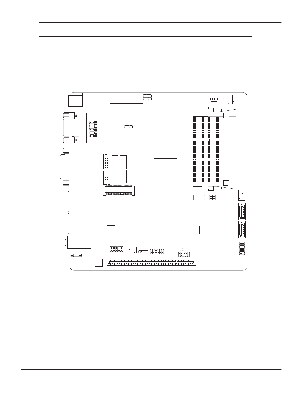
Mainboard Layout
Mainboard Layout
Top: LAN Jack
Bottom: USB Ports
Top: LAN Jack
Bottom: USB Ports
Top: VGA Port
Bottom: DVI-D Port
Top:
COM1
Bottom:
COM2
T: Line-In
M: Line-Out
B: Mic-In
JAUD1 SYSFAN1
CPUFAN1
JSEL1
JVDD1
PCI1
DIMM1
DIMM2
JGPIO1
JUSB1
JPWR1
JSPI1
JBAT1
SATA1
SATA2
JCOMP1
JCOMP2
JCOMP3
JCOMP4
JCOMP5
JCOMP6
JLPT1
CON1
JAMP1
JINV1
JKB_MS1
JLVDS1
JPWR2
JCI1
JFP1
JUSB2
COM4
COM3
COM6
COM5
Page 12

This chapter provides you with the information on
mainboard hardware confi gurations. Incorrect setting
of jumpers and connectors may damage your mainboard. Please pay special attention not to connect
these headers in wrong direction. DO NOT adjust any
jumper while the mainboard is powered on.
Chapter 2
Hardware Setup
Page 13
2-2
▍ Hardware Setup
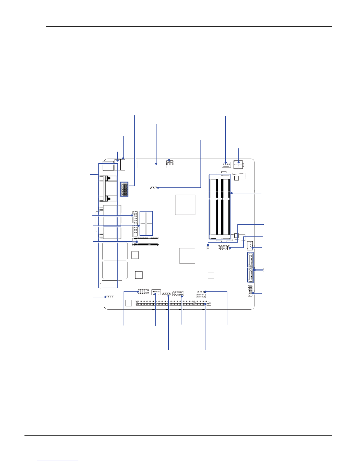
Quick Components Guide
Quick Components Guide
SATA Connector, p.2-8
Back Panel I/O,
p.2-5
Chassis Intrusion
Connector, p.2-8
LVDS Connector, p.2-14
PCI Slot, p.2-18
Serial Port
Connector,
p.2-13
Keyboard/Mouse
Connector, p.2-10
Parallel Port
Connector,
p.2-12
Amplifi er
Connector,
p.2-9
DIMM Slot,
p.2-3
Front Panel Connector, p.2-10
Front USB Connector,
p.2-11
Fan Power
Connector,
p.2-9
LVDS Inverter
Connector, p.2-14
Mini PCI-E
Slot, p.2-18
GPIO
Connector,
p.2-12
DC Power
Connector,
p.2-4
SATA Power
Connector, p.2-4
Clear CMOS
Jumper, p.2-16
COM Power Select
Jumper, p.2-17
AT/ATX Power Select
Jumper, p.2-17
Front Audio
Connectort,
p.2-15
LVDS Power
Jumper, p.2-17
Fan Power
Connector,
p.2-9
Front USB
Connector,
p.2-11
Page 14

2-3
MX255D
Memory
Memory
INSTALLING MEMORY MODULES
1. Locate the SO-DIMM slot. Align the notch on the DIMM with the key on
the slot and insert the DIMM into the slot.
2. Push the DIMM gently downwards until the slot levers click and lock
the DIMM in place.
3. To uninstall the DIMM, fl ip the slot levers outwards and the DIMM will
be released instantly.
Important
Important
You can barely see the golden fi nger if the memory module is properly in-
serted in the DIMM slot.
Page 15
2-4
▍ Hardware Setup
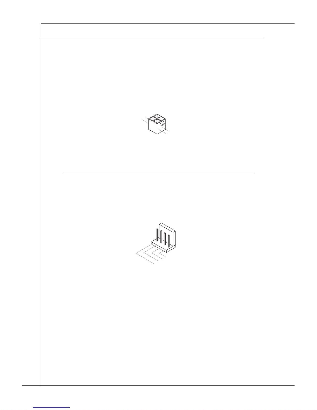
DC POWER CONNECTOR: JPWR1
This DC-In connector provides 12V power input.
4.DC
P
owe
r
2.Ground
3.DC
P
owe
r
1
.Ground
SATA Power Connector: JPWR2
This DC-In connector provides DC power output for SATA devices.
4+12V
3.GND
2.GND
1.VCC
5
Power Supply
Power Supply
Page 16
2-5
MX255D
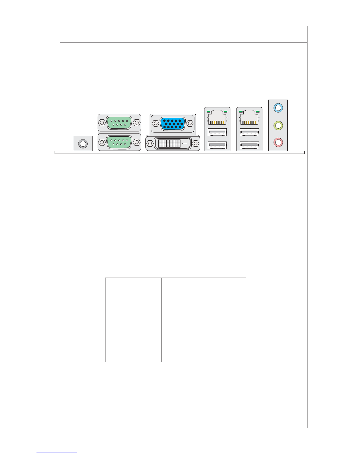
Back Panel I/OBack Panel I/O
▶ DC Power Jack
▶ COM1: RS-232/422/485 Serial Port
The serial port is a 16550A high speed communications port that sends/
receives 16 bytes FIFOs. You can attach a serial mouse or other serial devices directly to the connector.
PIN SIGNAL DESCRIPTION
1
2
3
4
5
6
7
8
9
DCD
RXD
TXD
DTR
GND
DSR
RTS
CTS
VCC_COM1
Data Carrier Detect
Receive Data
Transmit Data
Data Terminal Ready
Signal Ground
Data Set Ready
Request To Send
Clear To Send
Voltage select setting by jumper
RS-232
RS-232/422/485
Serial Port
DVI-D Port
VGA Port
LAN Jack
USB 2.0 Ports
Line-In Jack
Line-Out Jack
Mic Jack
LAN Jack
USB 2.0 PortsRS-232
Serial Port
DC Powr Jack
Page 17

2-6
▍ Hardware Setup
PIN SIGNAL DESCRIPTION
1
2
3
4
5
6
7
8
9
422 TXD422 RXD+
422 TXD+
422 RXDGND
NC
NC
NC
NC
Transmit Data, Negative
Receive Data, Positive
Transmit Data, Positive
Receive Data, Negative
Signal Ground
No Connection
No Connection
No Connection
No Connection
RS-422
PIN SIGNAL DESCRIPTION
1
2
3
4
5
6
7
8
9
485 TXDNC
485 TXD+
NC
GND
NC
NC
NC
NC
Transmit Data, Negative
No Connection
Transmit Data, Positive
No Connection
Signal Ground
No Connection
No Connection
No Connection
No Connection
RS-485
▶ COM2: RS-232 Serial Port
The serial port is a 16550A high speed communications port that sends/ receives 16 bytes FIFOs. You can attach a serial mouse or other serial devices
directly to the connector.
▶ VGA Port
The DB15-pin female connector is provided for monitor.
▶ DVI-D Port
The DVI-D (Digital Visual Interface-Digital) connector allows you to connect
an LCD monitor. It provides a high-speed digital interconnection between the
computer and its display device. To connect an LCD monitor, simply plug
your monitor cable into the DVI connector, and make sure that the other end
Page 18
2-7
MX255D
of the cable is properly connected to your monitor (refer to your monitor
manual for more information.)
▶ USB 2.0 Port
The USB (Universal Serial Bus) port is for attaching USB devices such as
keyboard, mouse, or other USB-compatible devices.
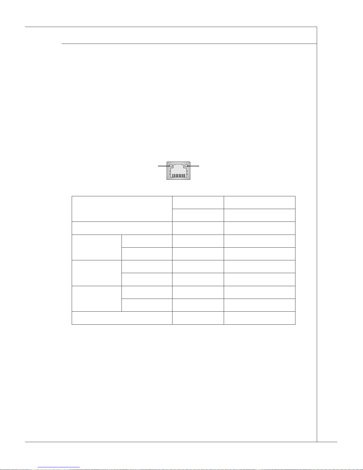
▶ LAN Jack
The standard RJ-45 LAN jack is for connection to the Local Area Network
(LAN). You can connect a network cable to it.
Speed IndicatorActivity Indicator
Left LED Right LED
Active LED 100M/1000M Speed LED
LED Color
Yellow
Yellow
Green
Green/
Orange
Orange
10M Cable
Plug-in
No Transmission
Yellow
Yellow (Lighting) OFF
Transmission
Yellow
Yellow (Blinking) OFF
100M Cable
Plug-in
No Transmission
Yellow
Yellow (Lighting)
Green
Green (Lighting)
Transmission
Yellow
Yellow (Blinking)
Green
Green (Lighting)
1000M Cable
Plug-in
No Transmission
Yellow
Yellow (Lighting)
Orange
Orange (Lighting)
Transmission
Yellow
Yellow (Blinking)
Orange
Orange (Lighting)
In S3/S4/S5 Standby State
Yellow
Yellow (Lighting) OFF
▶ Audio Jack
■ Line-In (Blue) - for external CD player or other audio devices
■ Line-Out (Green) - for speakers or headphones
■ Mic-In (Pink) - for microphones
Page 19
2-8
▍ Hardware Setup
Connector
Connector
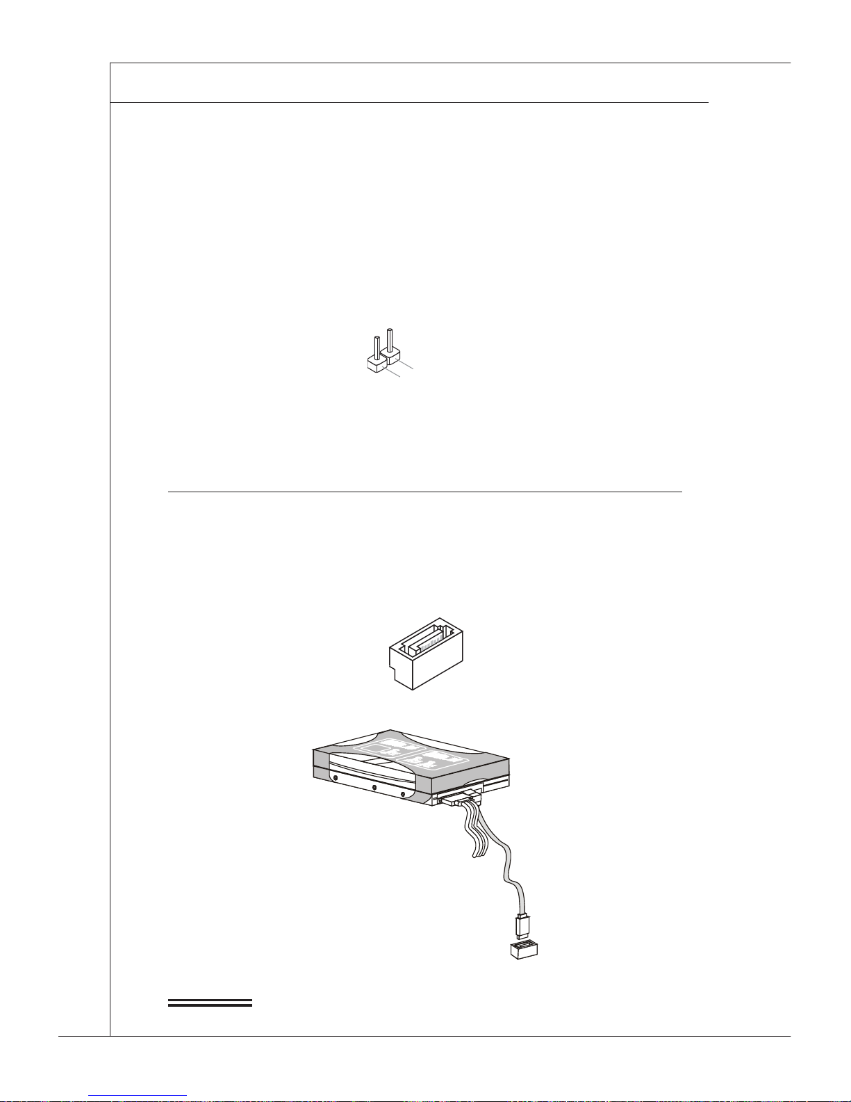
CHASSIS INTRUSION CONNECTOR: JCI1
This connector is provided to connect the chassis intrusion switch cable. If
the chassis is opened, the chassis intrusion mechanism will be activated.
The system will record this status and show a warning message on the
screen. To clear the warning, you must enter the BIOS utility and clear the
record.
1
.
C
I
N
T
R
U
2
.
G
r
o
u
n
d
Serial ATA Connector: SATA1 ~ SATA2
This connector is a high-speed Serial ATA interface port. Each connector
can connect one Serial ATA device.
Important
Important
Please do not fold the Serial ATA cable into 90-degree angle. Otherwise,
Page 20
2-9
MX255D
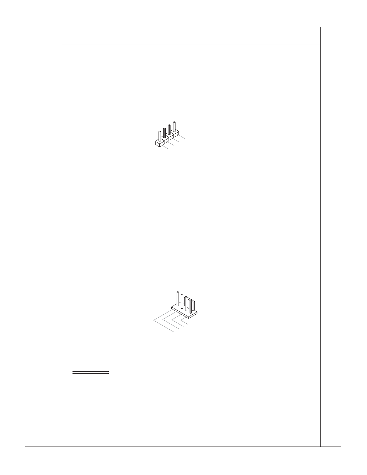
AUDIO AMPLIFIER CONNECTOR: JAMP1
The JAMP1 is used to connect audio amplifi ers to enhance audio perfor-
mance.
2.AMP_L+
1.AMP_
L
-
4.AMP_R
+
3.AMP_R-
Fan Power Connector: CPUFAN1, SYSFAN1
The fan power connector supports system cooling fan with +12V. When
connecting the wire to the connectors, always note that the red wire is the
positive and should be connected to the +12V; the black wire is Ground and
should be connected to GND. If the mainboard has a System Hardware
Monitor chipset onboard, you must use a specially designed fan with speed
sensor to take advantage of the CPU fan control.
1
.
G
r
o
u
n
d
2
.
+
1
2
V
3
.
S
e
n
s
o
r
4
.
C
o
n
t
r
o
l
Important
Important
• Please refer to the recommended CPU fans at processor’s offi cial web-
site or consult the vendors for proper CPU cooling fan.
• Fan cooler set with 3- or 4-pin power connector are both available for
CPUFAN1.
Page 21
2-10
▍ Hardware Setup
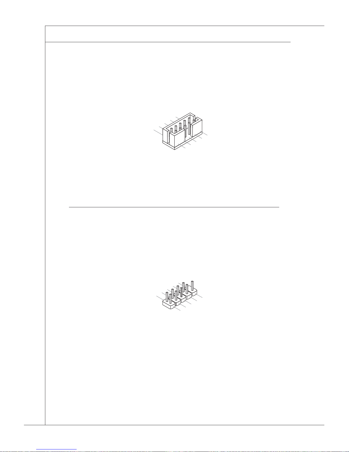
KEYBOARD/MOUSE CONNECTOR: JKB_MS1
This connector is used to connect PS/2 keyboard & mouse.
10.NC
8.GND
6
.KBCLK_PH#
4.KBDAT_PH#
2.KBMS_Power
1.KBMS_Powe
r
3.MSDAT_PH#
5.MSCLK_PH#
7.GND
9.NC
Front Panel Connector: JFP1
This front panel connector is provided for electrical connection to the front
panel switches & LEDs and is compliant with Intel Front Panel I/O Connectivity Design Guide.
1.HDD_LED
+
3.HDD_LED-
10.No
P
in
5.Reset_SW-
7.Reset_SW+
9.Reserved
8.Power_SW-
6.Power_SW+
4.Power_LED-
2.Power_LED+
Page 22
2-11
MX255D
Important
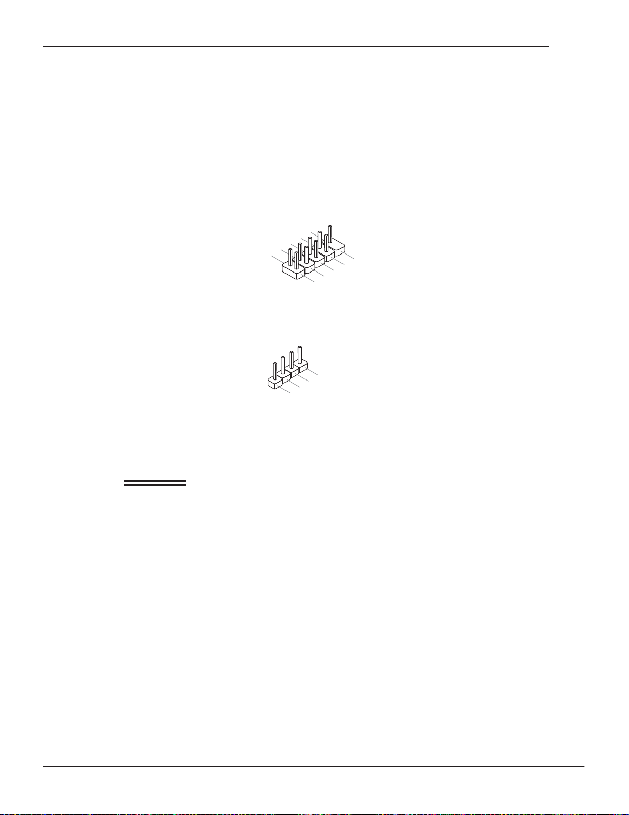
FRONT USB CONNECTOR: JUSB1, JUSB2
This connector, compliant with Intel I/O Connectivity Design Guide, is ideal
for connecting high-speed USB interface peripherals such as USB HDD,
digital cameras, MP3 players, printers, modems and the like.
1.VC
C
3.USB0-
10.NC
5.USB0+
7.Ground
9.No
P
i
n
8.Ground
6.USB1+
4.USB1-
2.VCC
2.Data-
1.Power
4.Ground
3.Data+
Important
Important
Note that the pins of VCC and GND must be connected correctly to avoid
possible damage.
Page 23
2-12
▍ Hardware Setup
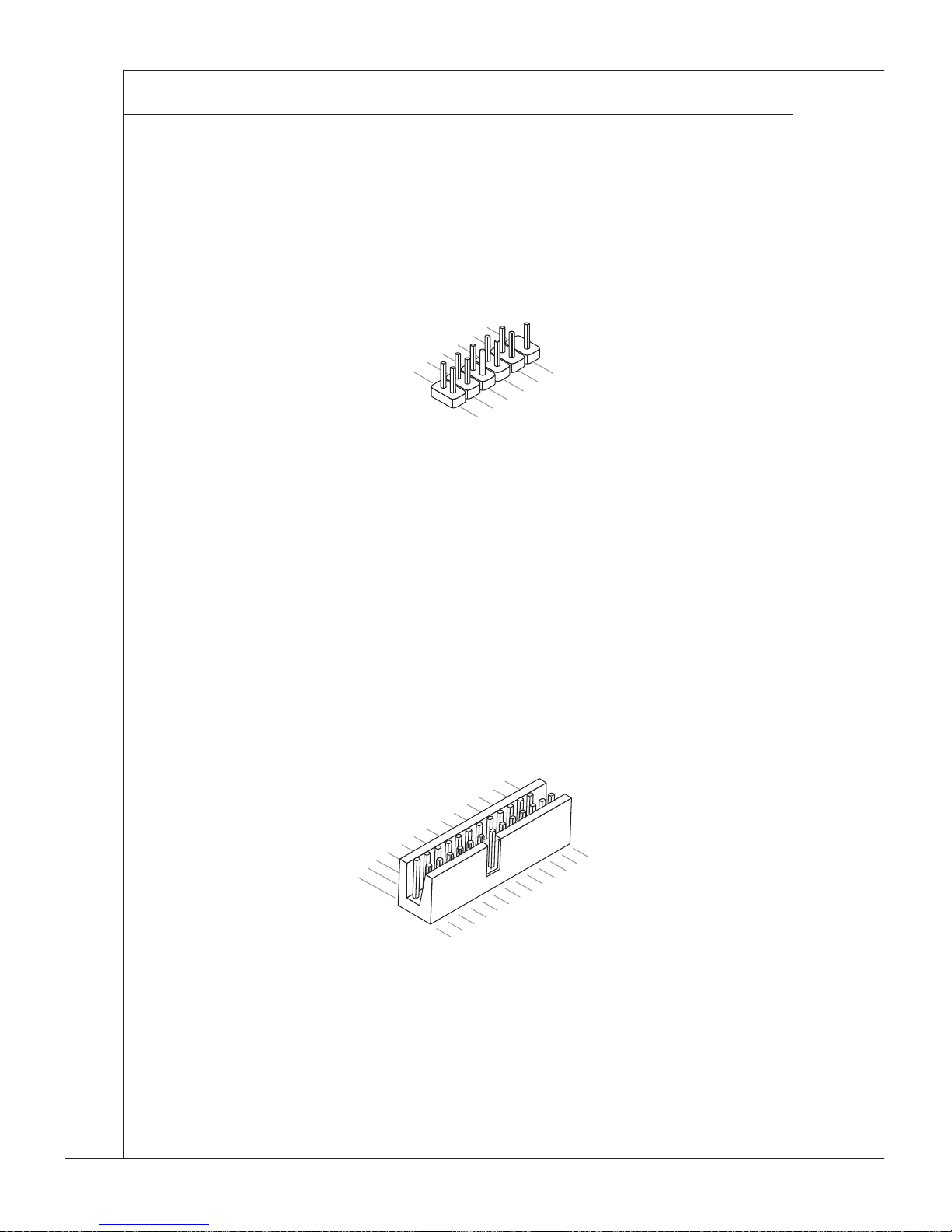
GPIO CONNECTOR: JGPIO1
This connector is provided for the General-Purpose Input/Output (GPIO)
peripheral module.
8.GPIO
O
utput 2
6.GPIO
O
utput 1
4.GPIO
O
utput 0
1.+12V
3.GPIO
I
nput
0
1
0.GPIO
O
utput 3
5.GPIO
I
nput 1
7.GPIO
I
nput 2
9.GPIO
I
nput
3
2.VCC5
12.KEY
11.GND
Parallel Port Connector: JLPT1
The mainboard provides a 26-pin header for connection to an optional
parallel port bracket. The parallel port is a standard printer port that supports Enhanced Parallel Port (EPP) and Extended Capabilities Parallel Port
(ECP) mode.
1.RSTB
#
3.PRND0
5.PRND1
7.PRND2
9.PRND3
11.PRND4
13.PRND5
15.PRND6
17.PRND7
19.ACK#
21.BUSY
23.PE
25.SLCT
10.Ground
14.Ground
8.LPT_SLIN#
12.Ground
6.PINIT#
4.ERR#
2.AFD#
24.Ground
22.Ground
2
6.No Pin
20.Ground
18.Ground
16.Ground
Page 24
2-13
MX255D
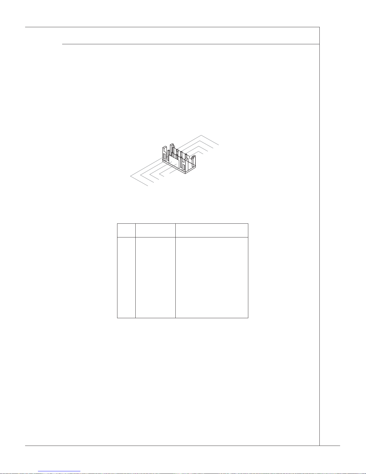
RS-232 SERIAL PORT CONNECTOR: COM3, COM4,
COM5, COM6
This connector is a 16550A high speed communications port that sends/
receives 16 bytes FIFOs. You can attach a serial device to it through an
optional serial port bracket.
8.CTS
3.TXD
1.DC
D
6.DSR
5.GND
4.DTR
7.RTS
2.RX
D
9.VCC_COM
PIN SIGNAL DESCRIPTION
1
2
3
4
5
6
7
8
9
DCD
RXD
TXD
DTR
GND
DSR
RTS
CTS
VCC_COM
Data Carrier Detect
Receive Data
Transmit Data
Data Terminal Ready
Signal Ground
Data Set Ready
Request To Send
Clear To Send
12V or 5V power output,
selected by JCOMP
Page 25
2-14
Hardware Setup
▍
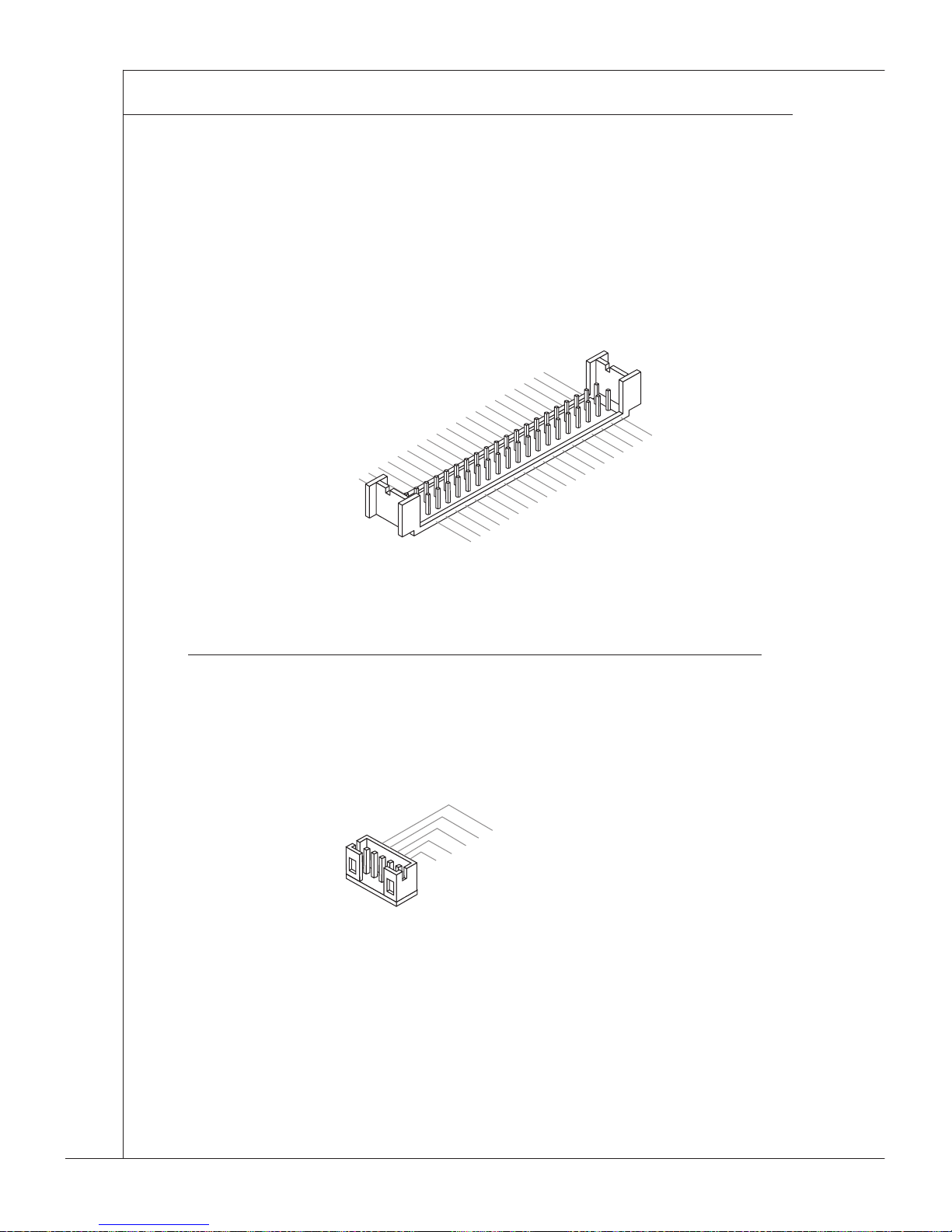
LVDS Connector: JLVDS1
The LVDS (Low Voltage Differential Signal) connector provides a digital in-
terface typically used with at panels. After connecting an LVDS interface
at panel to the JLVDS1, be sure to check the panel datasheet and set the
JVDD1 jumper to proper power voltage.
39.G ND
27.G ND
25.
LVDS1_D ATA 3 N
23.LVDS 1_ CKN
21.LVDS 1_ DATA 2 N
19.LVDS 1_ DATA1 N
17.LVDS 1_ DATA0 N
15.B ackligh t Ena ble
13.B ackligh t Con trol
11.LDDC _C LK
9.LC D_VDD
7.+3 .3V
5.+1 2V
3.+1 2V
1.+1 2V
40.G ND
28.G ND
26.
LVDS1_D ATA 3 P
24.LVDS 1_ CKP
22.LVDS 1_ DATA 2 P
20.LVDS 1_ DATA1 P
18.LVDS 1_ DATA0 P
16.G ND
14.LVDS _V DDEN
12.L DDC_DATA
10.L CD_VDD
8.GN D
6.GN D
4.+1 2V
2.+1 2V
37.
LVDS2_D ATA 3 N
35.LVDS 2_ CKN
33.LVDS 2_ DATA 2 N
31.LVDS 2_ DATA1 N
29.LVDS 2_ DATA0 N
38.
LVDS2_D ATA 3 P
36.LVDS 2_ CKP
34.LVDS 2_ DATA 2 P
32.LVDS 2_ DATA1 P
30.LVDS 2_ DATA0 P
LCD Inverter Connector: JINV1
The connector is provided for LCD backlight options.
2.GND
3.
LVDS_BLON
4.
L_BKLT_CTRL#
5.VCC5
1.+12V
Page 26

2-15
MX255D
FRONT AUDIO CONNECTOR: JAUD1
This connector allows you to connect the front panel audio and is compliant
with Intel® Front Panel I/O Connectivity Design Guide.
1.MIC L
3.MIC R
1
0.Head Phone Detection
5.Head Phone R
7.SENSE_SEND
9.Head Phone
L
8.No Pin
6.MIC Detection
4.PRESENCE#
2.Ground
Page 27

2-16
▍ Hardware Setup
Jumper
Jumper
CLEAR CMOS JUMPER: JBAT1
There is a CMOS RAM onboard that has a power supply from an external
battery to keep the data of system confi guration. With the CMOS RAM, the
system can automatically boot OS every time it is turned on. If you want to
clear the system confi guration, set the jumper to clear data.
JBAT1
11
Normal
Clear CMOS
1
Important
Important
You can clear CMOS by shorting 2-3 pin while the system is off. Then return
to 1-2 pin position. Avoid clearing the CMOS while the system is on; it will
damage the mainboard.
Page 28
2-17
MX255D
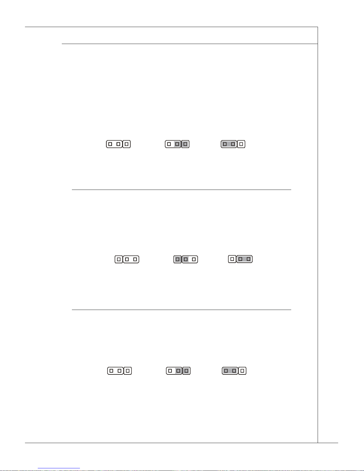
COM POWER SELECT JUMPER: JCOMP1 ~
JCOMP6
These jumpers are used to select the pin 9 power voltage of the COM1 ~
COM6 serial ports.
JCOMP1~6
11
+5V +12V
1
LVDS Power Jumper: JVDD1
The LVDS power jumper allows users to select the operation voltage of the
LVDS fl at panel.
JVDD1
11
3V
5V
1
AT/ATX Select Jumper: J1
This jumper allows users to select between AT and ATX power.
J1
11
AT
ATX
(Default)
1
Page 29
2-18
▍ Hardware Setup
Slot
Slot
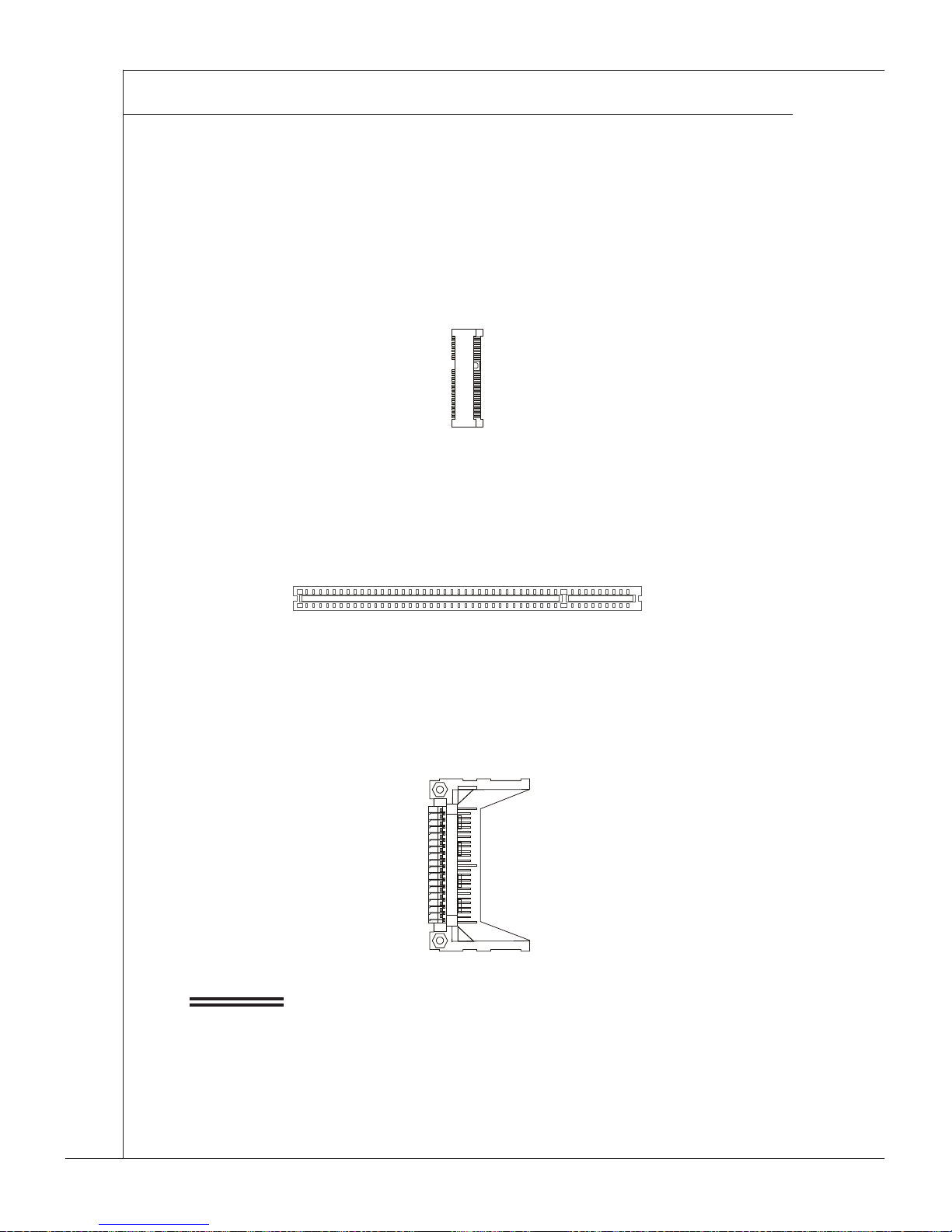
MINI PCI-E (PERIPHERAL COMPONENT INTERCONNECT EXPRESS) SLOT
The Mini PCI-E slot is provided for wireless LAN card, TV tuner card, and
Robson NAND Flash card.
Important
Important
When adding or removing expansion cards, make sure that you unplug the
power supply fi rst. Meanwhile, read the documentation for the expansion
card to confi gure any necessary hardware or software settings for the ex-
pansion card, such as jumpers, switches or BIOS confi guration.
PCI (PERIPHERAL COMPONENT INTERCONNECT)
SLOT
The PCI slot supports LAN card, SCSI card, USB card, and other add-on
COMPACTFLASH SOCKET
This socket supports CompactFlash cards.
Page 30

This chapter provides information on the BIOS Setup
program and allows you to confi gure the system for
optimum use.
You may need to run the Setup program when:
■ An error message appears on the screen
during the system booting up, and requests
you to run SETUP.
■ You want to change the default settings for
customized features.
Chapter 3
BIOS Setup
Page 31

3-2
▍ BIOS Setup
Entering Setup
Entering Setup
Power on the computer and the system will start POST (Power On Self Test)
process. When the message below appears on the screen, press <DEL>
key to enter Setup.
PRESS DEL TO ENTER SETUP
If the message disappears before you respond and you still wish to enter
Setup, restart the system by turning it OFF and On or pressing the RESET
button. You may also restart the system by simultaneously pressing <Ctrl>,
<Alt>, and <Delete> keys.
Page 32

3-3
MX255D
CONTROL KEYS
← → Select Screen
↑ ↓ Select Item
+ - Change Field
Tab Select Field
F1 General Help
F10 Save and Exit
Esc Exit
GETTING HELP
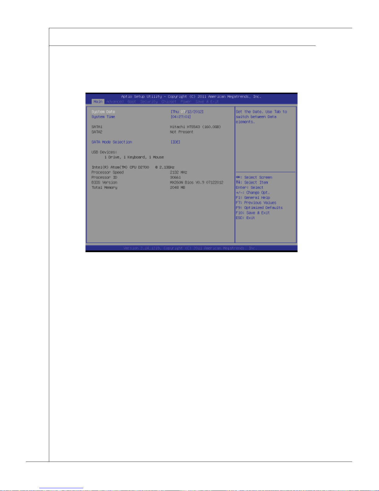
After entering the Setup menu, the fi rst menu you will see is the Main
Menu.
Main Menu
The main menu lists the setup functions you can make changes to. You can
use the arrow keys ( ↑↓ ) to select the item. The on-line description of the
highlighted setup function is displayed at the bottom of the screen.
Sub-Menu
If you fi nd a right pointer symbol appears to the left of certain fi elds that
means a sub-menu can be launched from this fi eld. A sub-menu contains
additional options for a fi eld parameter. You can use arrow keys ( ↑↓ ) to
highlight the fi eld and press <Enter> to call up the sub-menu. Then you can
use the control keys to enter values and move from fi eld to fi eld within a
sub-menu. If you want to return to the main menu, just press the <Esc >.
GENERAL HELP <F1>
The BIOS setup program provides a General Help screen. You can call up
this screen from any menu by simply pressing <F1>. The Help screen lists
the appropriate keys to use and the possible selections for the highlighted
item. Press <Esc> to exit the Help screen.
Page 33
3-4
▍ BIOS Setup
The Menu Bar
The Menu Bar
▶ Main
Use this menu for basic system confi gurations, such as time, date etc.
▶ Advanced
Use this menu to set up the items of special enhanced features.
▶ Boot
Use this menu to specify the priority of boot devices.
▶ Security
Use this menu to set supervisor and user passwords.
▶ Chipset
This menu controls the advanced features of the onboard Northbridge and
Southbridge.
▶ Power
Use this menu to specify your settings for power management.
▶ Exit
This menu allows you to load the BIOS default values or factory default settings into the BIOS and exit the BIOS setup utility with or without changes.
Page 34
3-5
MX255D
Main
Main
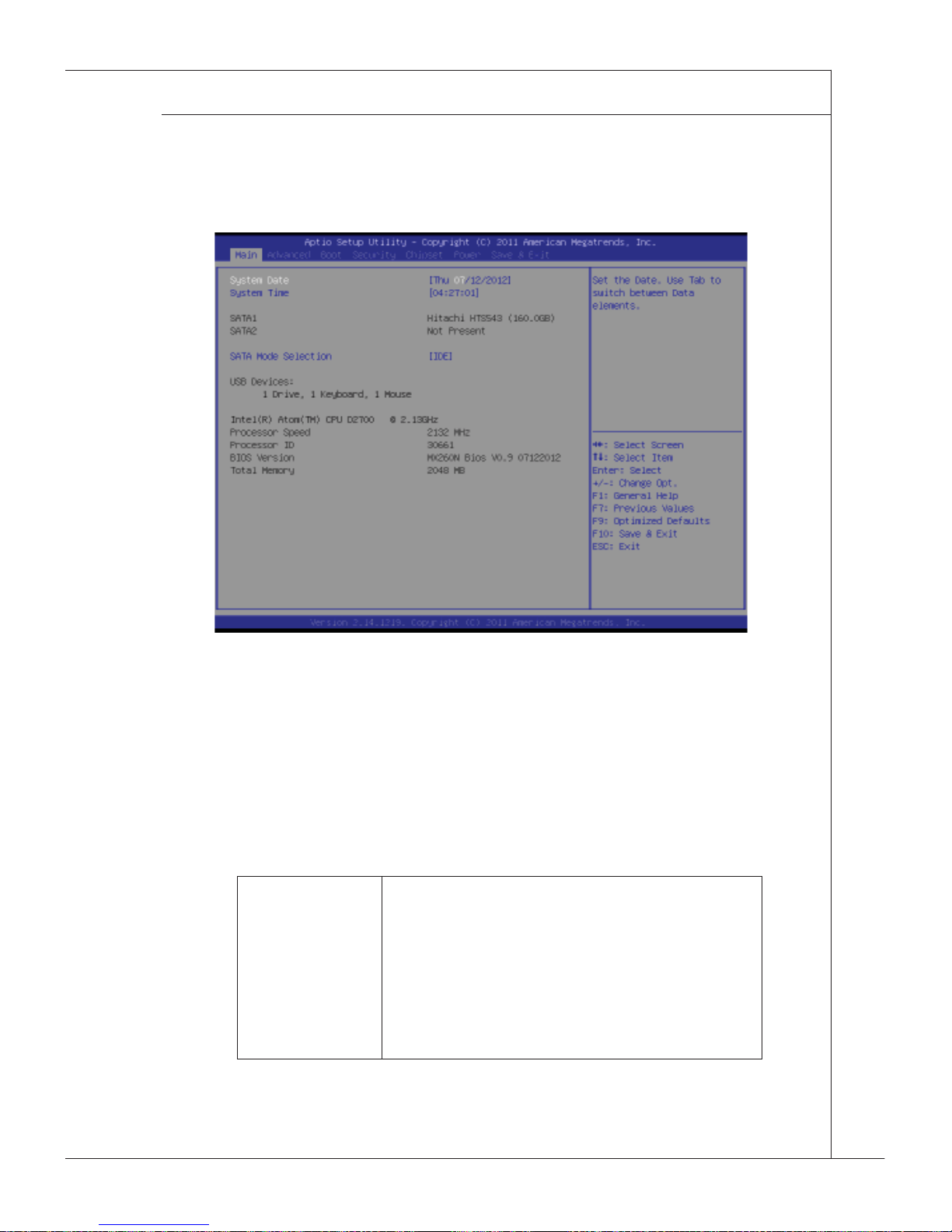
▶ System Time
This setting allows you to set the system time. The time format is <Hour>
<Minute> <Second>.
▶ System Date
This setting allows you to set the system date. The date format is <Day>,
<Month> <Date> <Year>.
▶ SATA1, SATA2
[Type] Press PgUp/<+> or PgDn/<-> to select
[Manual], [None] or [Auto] type. Note that the
specifi cations of your drive must match with
the drive table. The hard disk will not work
properly if you enter improper information for
this category. If your hard disk drive type is
not matched or listed, you can use [Manual] to
defi ne your own drive type manually.
Page 35

3-6
▍ BIOS Setup
[LBA/Large
Mode]
Enabling LBA causes Logical Block Addressing to be used in place of Cylinders, Heads
and Sectors
[Block
(Multi-Sector
Transfer)]
Any selection except Disabled determines the
number of sectors transferred per block
[PIO Mode] Indicates the type of PIO (Programmed
Input/Output)
[DMA Mode] Indicates the type of Ultra DMA
[S.M.A.R.T.] This allows you to activate the S.M.A.R.T.
(Self-Monitoring Analysis & Reporting Technology) capability for the hard disks. S.M.A.R.T
is a utility that monitors your disk status to
predict hard disk failure. This gives you an
opportunity to move data from a hard disk that
is going to fail to a safe place before the hard
disk becomes offl ine.
[32 Bit Data
Transfer]
Enables 32-bit communication between
CPU and IDE controller
▶ SATA Mode Selection
This setting specifi es the SATA controller mode.
Page 36
3-7
MX255D
Advanced
Advanced
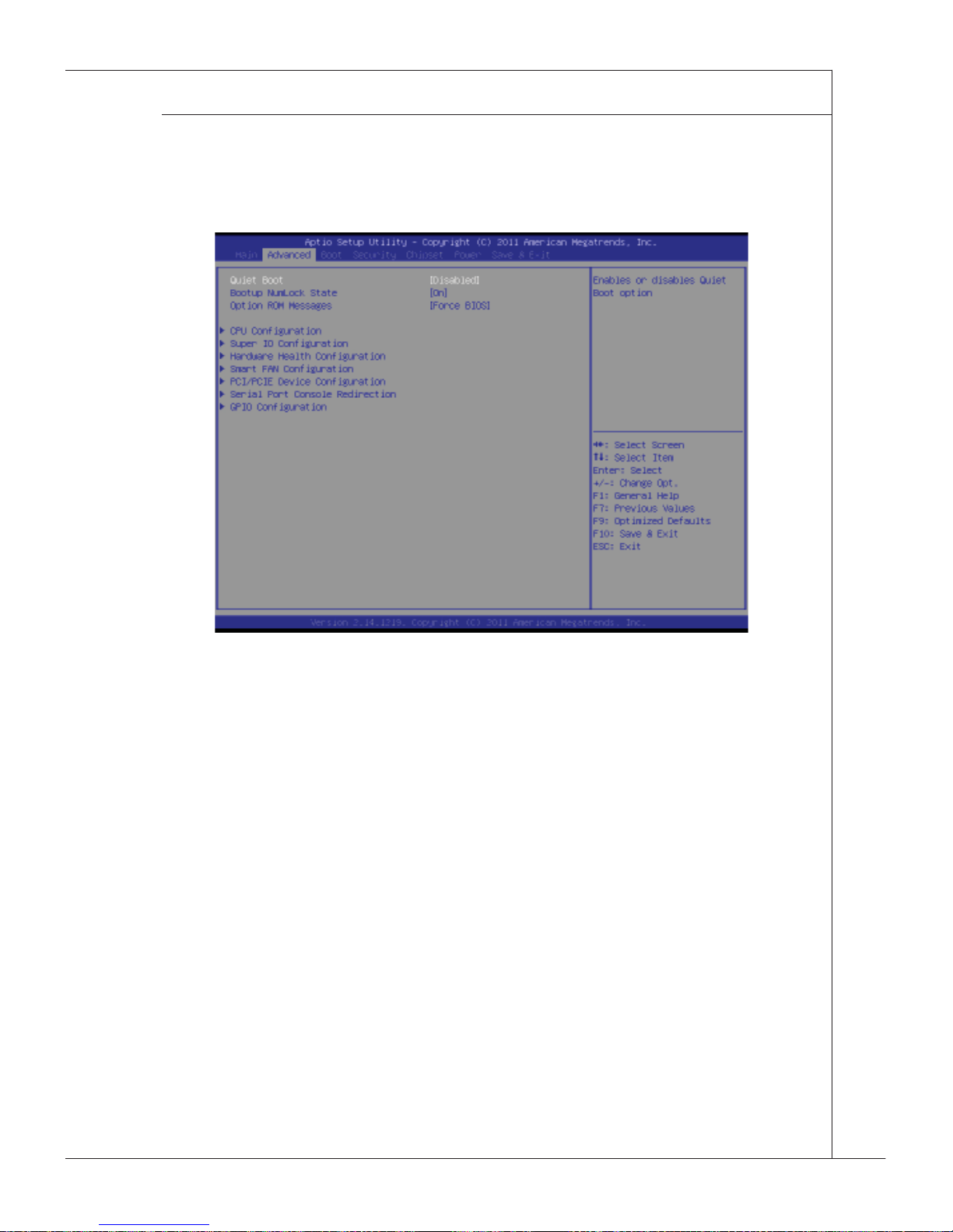
▶ Quick Boot
Enabling this setting will cause the BIOS power-on self test routine to skip
some of its tests during bootup for faster system boot.
▶ Bootup Num-Lock
This setting is to set the Num Lock status when the system is powered on.
Setting to [On] will turn on the Num Lock key when the system is powered
on. Setting to [Off] will allow users to use the arrow keys on the numeric
keypad.
▶ Option ROM Messages
This item is used to determine the display mode when an optional ROM is
initialized during POST. When set to [Force BIOS], the display mode used
by AMI BIOS is used. Select [Keep Current] if you want to use the display
mode of optional ROM.
Page 37
3-8
▍ BIOS Setup
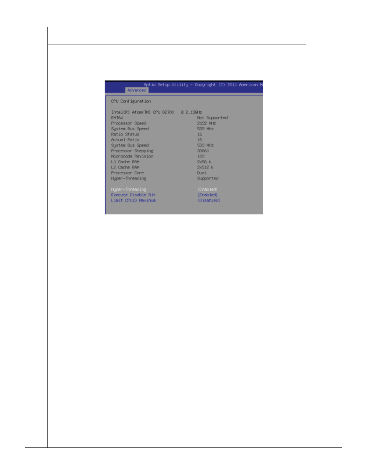
▶ CPU Confi guration
▶ Hyper-Threading
The processor uses Hyper-Threading technology to increase transaction rates and reduces end-user response times. The technology treats
the two cores inside the processor as two logical processors that can
execute instructions simultaneously. In this way, the system performance is highly improved. If you disable the function, the processor will
use only one core to execute the instructions. Please disable this item if
your operating system doesn’t support HT Function, or unreliability and
instability may occur.
▶ Execute Disable Bit
Intel’s Execute Disable Bit functionality can prevent certain classes of
malicious “buffer overfl ow” attacks when combined with a supporting
operating system. This functionality allows the processor to classify
areas in memory by where application code can execute and where it
cannot. When a malicious worm attempts to insert code in the buffer,
the processor disables code execution, preventing damage or worm
propagation.
▶ Limit CPUID Maximum
The Max CPUID Value Limit BIOS feature allows you to circumvent
problems with older operating systems that do not support the Intel
Pentium 4 processor with Hyper-Threading Technology. When enabled,
the processor will limit the maximum CPUID input value to 03h when
queried, even if the processor supports a higher CPUID input value.
Page 38
3-9
MX255D
When disabled, the processor will return the actual maximum CPUID
input value of the processor when queried.
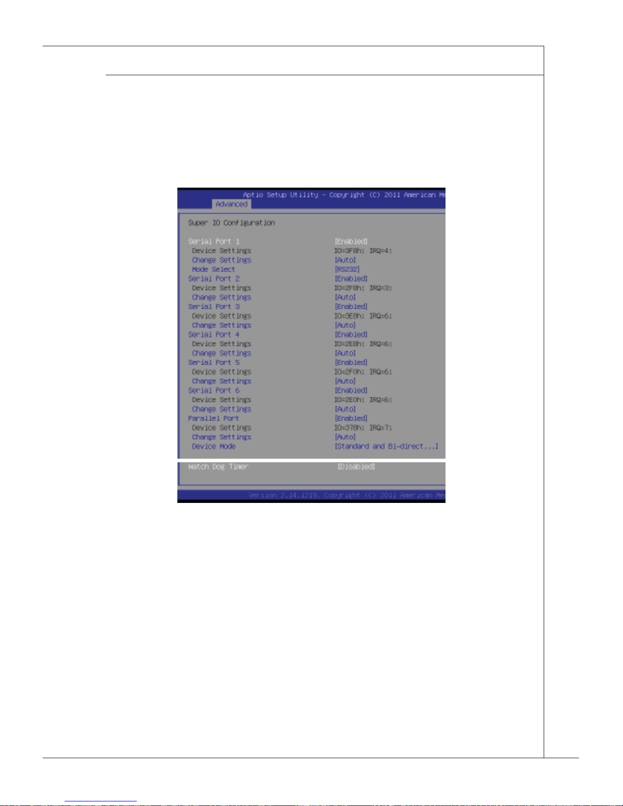
▶ Super IO Confi guration
▶ Serial Port 1/ 2/ 3/ 4/ 5/ 6/ Parallel Port Address
Select an address for the specifi ed serial/parallel port.
▶ Change Settings Serial Port 1/ 2/ 3/ 4/ 5/ 6 /Parallel Port
This setting is used to change the address & IRQ settings of the
specifi ed serial port.
▶ Mode Select
Select an operation mode for the serial port 1.
▶ Watch Dog
You can enable the system watch-dog timer, a hardware timer that generates a reset when the software that it monitors does not respond as
expected each time the watch dog polls it.
Page 39
3-10
▍ BIOS Setup
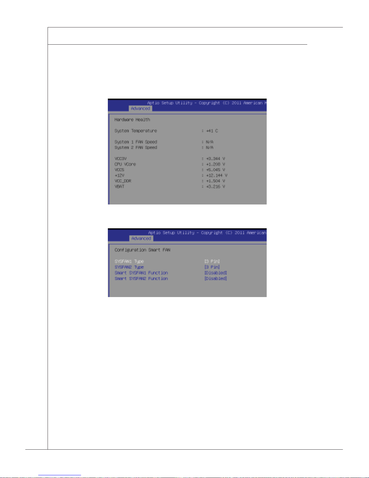
▶ Hardware Health Confi guration
These items display the current status of all monitored hardware devices/components such as voltages, temperatures and all fans’ speeds.
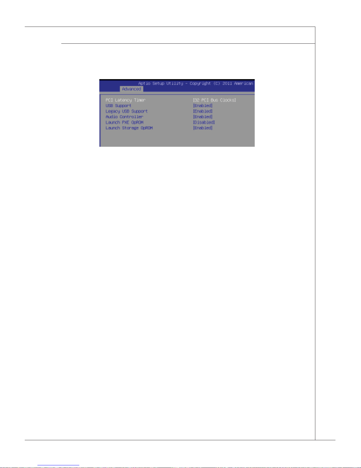
▶ Smart Fan Confi guration
▶ SYSFAN1 / 2 Type
This setting specifi es the fan type.
▶ Smart SYSFAN1 / 2 Function
This setting enables/disables the Smart Fan function. Smart Fan is an
excellent feature which will adjust the CPU/system fan speed automatically depending on the current CPU/system temperature, avoiding the
overheating to damage your system.
Page 40
3-11
MX255D
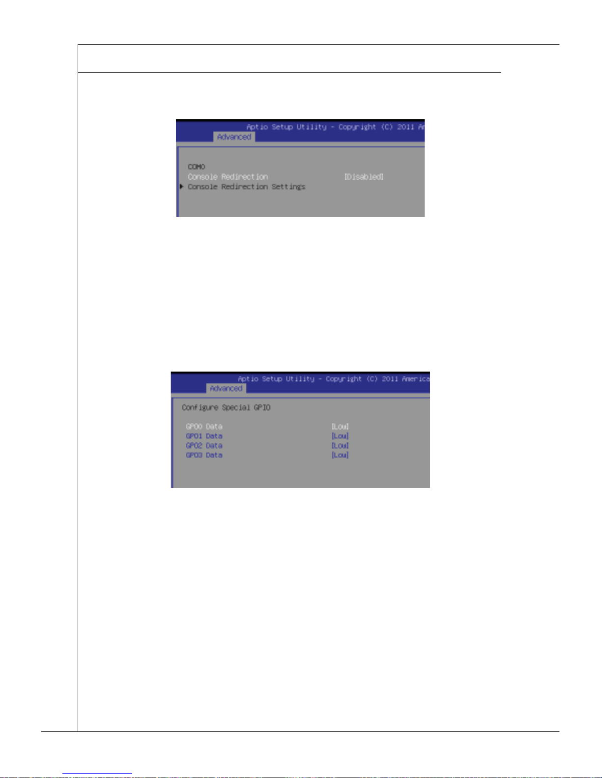
▶ PCI/PCIE Device Confi guration
▶ PCI Latency Timer
This item controls how long each PCI device can hold the bus before
another takes over. When set to higher values, every PCI device can
conduct transactions for a longer time and thus improve the effective
PCI bandwidth. For better PCI performance, you should set the item
to higher values.
▶ USB Support
This setting enables/disables the onboard USB controller.
▶ Legacy USB Support
Set to [Enabled] if you need to use any USB 1.1/2.0 device in the operating system that does not support or have any USB 1.1/2.0 driver
installed, such as DOS and SCO Unix.
▶ Audio Controller
This setting enables/disables the onboard audio controller.
▶ Launch PXE OpROM / Launch Storage OpROM
This setting enables/disables the initialization of the onboard LAN
Boot ROM during bootup. Selecting [Disabled] will speed up the boot
process.
Page 41
3-12
▍ BIOS Setup
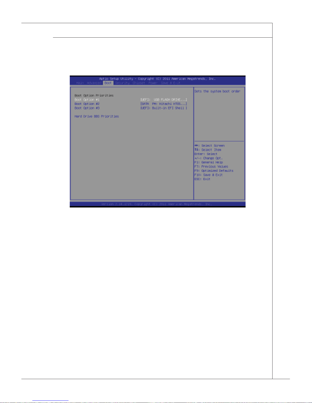
▶ Console Redirection
▶ Console Redirection Settings
Console Redirection operates in host systems that do not have a monitor and keyboard attached. This setting enables/disables the operation of console redirection. When set to [Enabled], BIOS redirects and
sends all contents that should be displayed on the screen to the serial
COM port for display on the terminal screen. Besides, all data received
from the serial port is interpreted as keystrokes from a local keyboard.
▶ GPIO Confi guration
▶ GPO 1/2/3/4 Data
This setting specifi es the GPO data.
Page 42
3-13
MX255D
Boot
Boot
▶ Boot Option #1 / 2 / 3
This setting allows users to set the sequence of boot devices where BIOS
attempts to load the disk operating system.
▶ Hard Drive BBS Priorities
This setting allows users to set the priority of the specifi ed devices. First
press <Enter> to enter the sub-menu. Then you may use the arrow keys ( ↑
↓ ) to select the desired device, then press <+>, <-> or <PageUp>, <PageDown> key to move it up/down in the priority list.
Page 43
3-14
▍ BIOS Setup
Security
Security
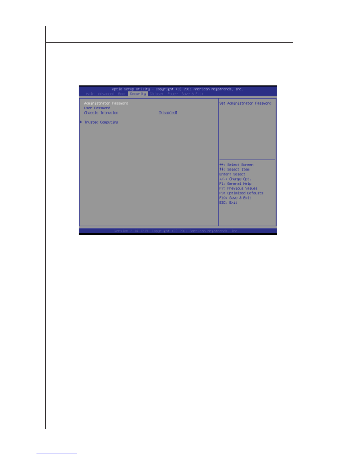
▶ Administrator Password
Administrator Password controls access to the BIOS Setup utility.
▶ User Password
User Password controls access to the system at boot and to the BIOS Setup
utility.
▶ Chassis Intrusion
The fi eld enables or disables the feature of recording the chassis intrusion
status and issuing a warning message if the chassis is once opened. To
clear the warning message, set the fi eld to [Reset]. The setting of the fi eld
will automatically return to the default value later.
Page 44
3-15
MX255D
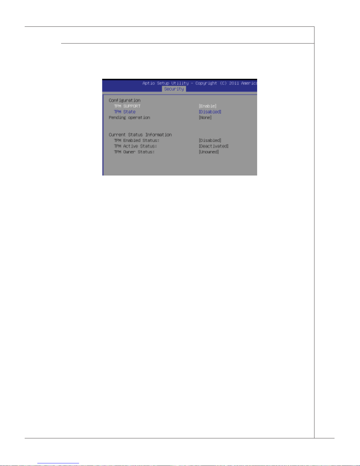
▶ Trusted Computing
▶ TCG/TPM Support
This setting controls the Trusted Platform Module (TPM) designed by
the Trusted Computing Group (TCG). TPMs are special-purpose integrated circuits (ICs) built into a variety of platforms to enable strong
user authentication and machine attestation - essential to prevent inappropriate access to confi dential and sensitive information and to protect
against compromised networks.
Page 45
3-16
▍ BIOS Setup
Chipset
Chipset
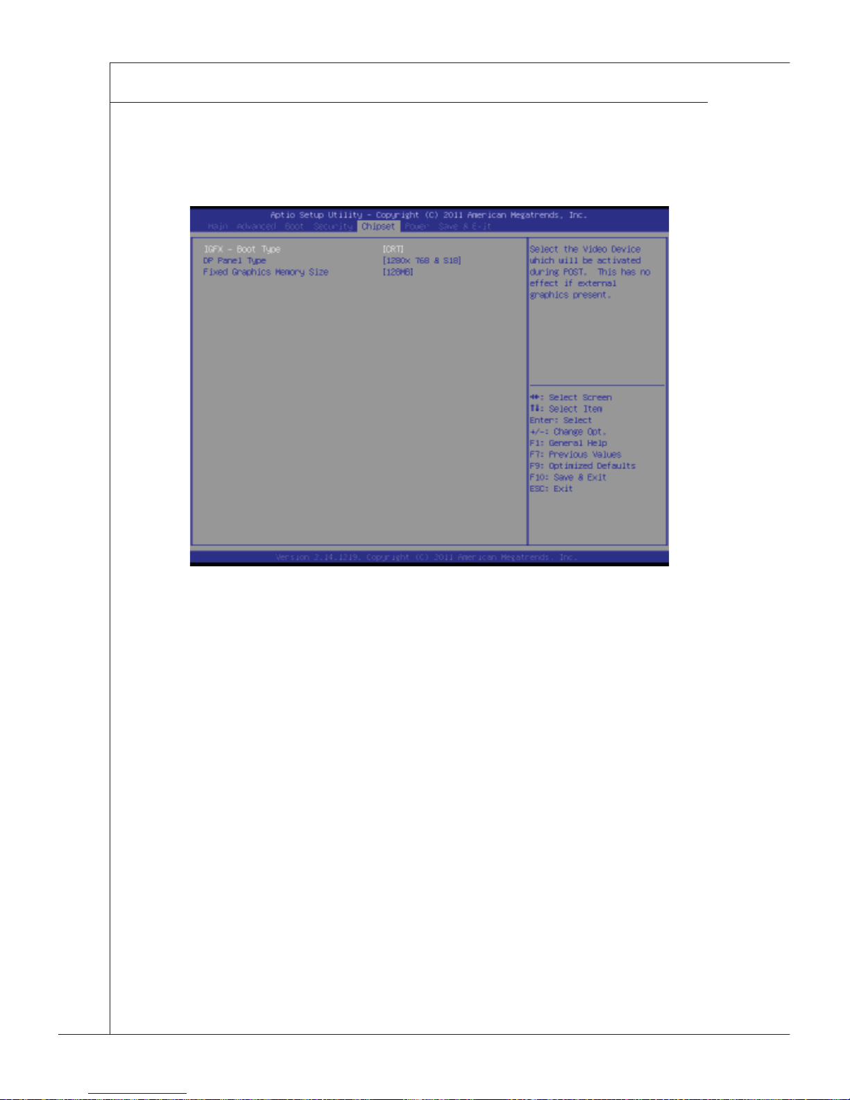
▶ IGFX - Boot Type
Use the fi eld to select the type of device you want to use as the boot display
of the system.
▶ DP Panel Type
This setting allows you to set your preferences for the boot display device.
▶ Fixed Graphics Memory Size
This setting specifi es the size of system memory allocated for video memory.
Page 46
3-17
MX255D
Power
Power
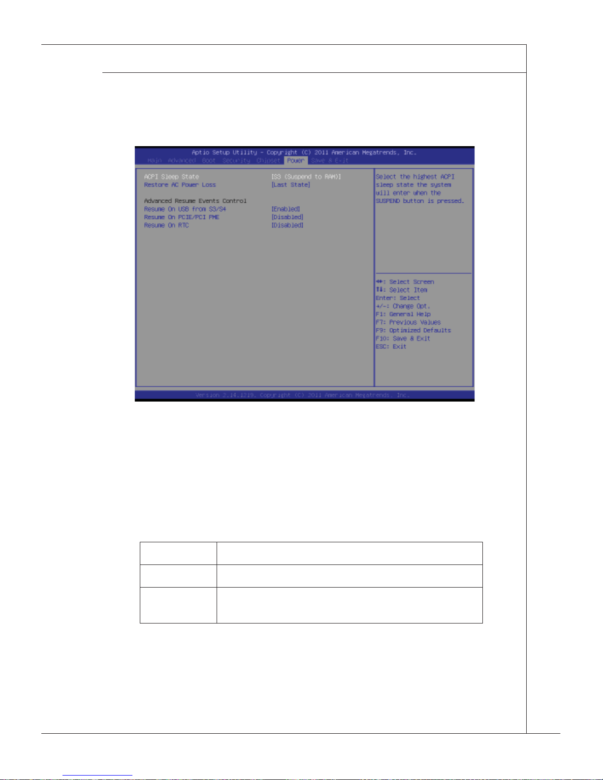
▶ ACPI Sleep State
This item specifi es the power saving modes for ACPI function. If your oper-
ating system supports ACPI, you can choose to enter the Standby mode in
S1 (POS) or S3 (STR) fashion through the setting of this fi eld.
▶ Restore on AC Power Loss
This setting specifi es whether your system will reboot after a power failure
or interrupt occurs. Available settings are:
[Power Off] Leaves the computer in the power off state.
[Power On] Leaves the computer in the power on state.
[Last State] Restores the system to the previous status before
power failure or interrupt occurred.
▶ Resume On USB from S3/S4
The item allows the activity of the USB device to wake up the system from
S3/S4 sleep state.
Page 47

3-18
▍ BIOS Setup
▶ Resume On PCIE/PCI PME
This fi eld specifi es whether the system will be awakened from power sav-
ing modes when activity or input signal of onboard PCIE/PCI PME is detected.This fi eld specifi es whether the system will be awakened from power
saving modes when activity or input signal of onboard LAN/mini PCI-E is
detected.
▶ Resume On RTC Alarm
When [Enabled], your can set the date and time at which the RTC (real-time
clock) alarm awakens the system from suspend mode.
Page 48
3-19
MX255D
Exit
Exit
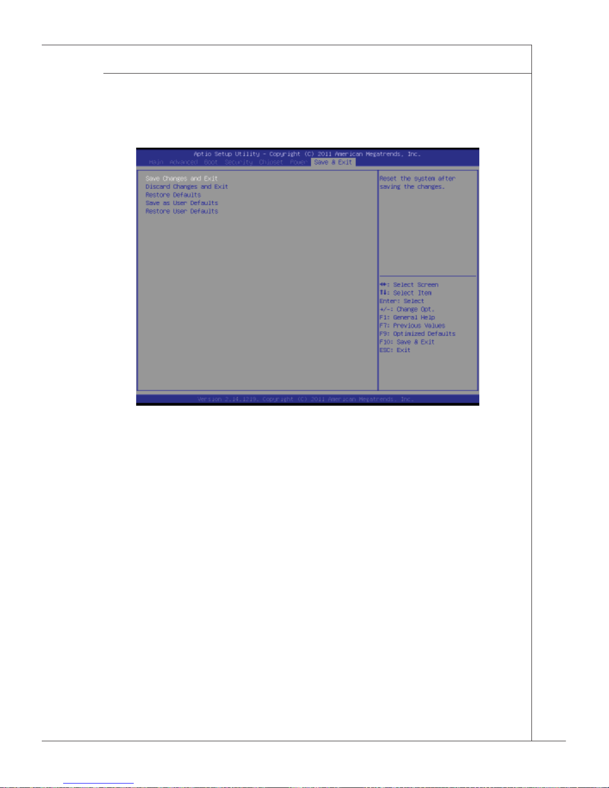
▶ Save Changes and Exit
Save changes to CMOS and exit the Setup Utility.
▶ Discard Changes and Exit
Abandon all changes and exit the Setup Utility.
▶ Restore Defaults
Restore the factory defaults.
▶ Save as User Defaults
Save all changes as user defaults.
▶ Restore User Defaults
Restore the preset user defaults.
Page 49

Page 50

This chapter provides information on system resources.
Chapter 4
System Resources
Page 51

4-2
▍ System Resources
AMI POST Code
AMI POST Code
Bootblock Initialization Code Checkpoints
The Bootblock initialization code sets up the chipset, memory and other
components before system memory is available. The following table describes the type of checkpoints that may occur during the bootblock initialization portion of the BIOS:
Checkpoint Description
Before D1
Early chipset initialization is done. Early super I/O initialization is done
including RTC and keyboard controller. NMI is disabled.
D1
Perform keyboard controller BAT test. Check if waking up from power
management suspend state. Save power-on CPUID value in scratch
CMOS.
D0
Go to fl at mode with 4GB limit and GA20 enabled. Verify the bootblock
checksum.
D2
Disable CACHE before memory detection. Execute full memory sizing
module. Verify that fl at mode is enabled.
D3
If memory sizing module not executed, start memory refresh and do
memory sizing in Bootblock code. Do additional chipset initialization.
Re-enable CACHE. Verify that fl at mode is enabled.
D4
Test base 512KB memory. Adjust policies and cache fi rst 8MB. Set
stack.
D5
Bootblock code is copied from ROM to lower system memory and control is given to it. BIOS now executes out of RAM.
D6
Both key sequence and OEM specifi c method is checked to determine
if BIOS recovery is forced. Main BIOS checksum is tested. If BIOS
recovery is necessary, control fl ows to checkpoint E0. See Bootblock
Recovery Code Checkpoints section of document for more information.
D7
Restore CPUID value back into register. The Bootblock-Runtime interface module is moved to system memory and control is given to it.
Determine whether to execute serial fl ash.
D8
The Runtime module is uncompressed into memory. CPUID information is stored in memory.
D9
Store the Uncompressed pointer for future use in PMM. Copying Main
BIOS into memory. Leaves all RAM below 1MB Read-Write including
E000 and F000 shadow areas but closing SMRAM.
Page 52

4-3
MX255D
POST Code Checkpoints
The POST code checkpoints are the largest set of checkpoints during the
BIOS pre-boot process. The following table describes the type of checkpoints that may occur during the POST portion of the BIOS:
Checkpoint Description
03
Disable NMI, Parity, video for EGA, and DMA controllers. Initialize
BIOS, POST, Runtime data area. Also initialize BIOS modules on
POST entry and GPNV area. Initialized CMOS as mentioned in the
Kernel Variable “wCMOSFlags.”
04
Check CMOS diagnostic byte to determine if battery power is OK and
CMOS checksum is OK. Verify CMOS checksum manually by reading storage area. If the CMOS checksum is bad, update CMOS with
power-on default values and clear passwords. Initialize status register
A. Initializes data variables that are based on CMOS setup questions.
Initializes both the 8259 compatible PICs in the system
05
Initializes the interrupt controlling hardware (generally PIC) and interrupt vector table.
06
Do R/W test to CH-2 count reg. Initialize CH-0 as system timer. Install
the POSTINT1Ch handler. Enable IRQ-0 in PIC for system timer interrupt. Traps INT1Ch vector to “POSTINT1ChHandlerBlock.”
08
Initializes the CPU. The BAT test is being done on KBC. Program the
keyboard controller command byte is being done after Auto detection
of KB/MS using AMI KB-5.
0A Initializes the 8042 compatible Key Board Controller.
0B Detects the presence of PS/2 mouse.
0C Detects the presence of Keyboard in KBC port.
0E
Testing and initialization of different Input Devices. Also, update the
Kernel Variables. Traps the INT09h vector, so that the POST INT09h
handler gets control for IRQ1. Uncompress all available language,
BIOS logo, and Silent logo modules.
Page 53

4-4
▍ System Resources
Checkpoint Description
13 Early POST initialization of chipset registers.
24 Uncompress and initialize any platform specifi c BIOS modules.
30 Initialize System Management Interrupt.
2A
Initializes different devices through DIM. See DIM Code Checkpoints
section of document for more information.
2C
Initializes different devices. Detects and initializes the video adapter
installed in the system that have optional ROMs.
2E Initializes all the output devices.
31
Allocate memory for ADM module and uncompress it. Give control to
ADM module for initialization. Initialize language and font modules for
ADM. Activate ADM module.
33
Initializes the silent boot module. Set the window for displaying text
information.
37
Displaying sign-on message, CPU information, setup key message,
and any OEM specifi c information.
38
Initializes different devices through DIM. See DIM Code Checkpoints
section of document for more information.
39 Initializes DMAC-1 & DMAC-2.
3A Initialize RTC date/time.
3B
Test for total memory installed in the system. Also, Check for DEL or
ESC keys to limit memory test. Display total memory in the system.
3C Mid POST initialization of chipset registers.
40
Detect different devices (Parallel ports, serial ports, and coprocessor
in CPU, … etc.) successfully installed in the system and update the
BDA, EBDA…etc.
50
Programming the memory hole or any kind of implementation that
needs an adjustment in system RAM size if needed.
52
Updates CMOS memory size from memory found in memory test. Allocates memory for Extended BIOS Data Area from base memory.
60 Initializes NUM-LOCK status and programs the KBD typematic rate.
75 Initialize Int-13 and prepare for IPL detection.
78 Initializes IPL devices controlled by BIOS and option ROMs.
7A Initializes remaining option ROMs.
7C Generate and write contents of ESCD in NVRam.
Page 54

4-5
MX255D
Checkpoint Description
84 Log errors encountered during POST.
85 Display errors to the user and gets the user response for error.
87 Execute BIOS setup if needed / requested.
8C Late POST initialization of chipset registers.
8E Program the peripheral parameters. Enable/Disable NMI as selected
90 Late POST initialization of system management interrupt.
A0 Check boot password if installed.
A1 Clean-up work needed before booting to OS.
A2
Takes care of runtime image preparation for different BIOS modules. Fill
the free area in F000h segment with 0FFh.
Initializes the Microsoft IRQ Routing Table. Prepares the runtime language module. Disables the system confi guration display if needed.
A4 Initialize runtime language module.
A7
Displays the system confi guration screen if enabled. Initialize the CPU’s
before boot, which includes the programming of the MTRR’s.
A8 Prepare CPU for OS boot including fi nal MTRR values.
A9 Wait for user input at confi g display if needed.
AA
Uninstall POST INT1Ch vector and INT09h vector. Deinitializes the
ADM module.
AB Prepare BBS for Int 19 boot.
AC End of POST initialization of chipset registers.
B1 Save system context for ACPI.
00 Passes control to OS Loader (typically INT19h).
Page 55
4-6
▍ System Resources
Resource List
Resource List
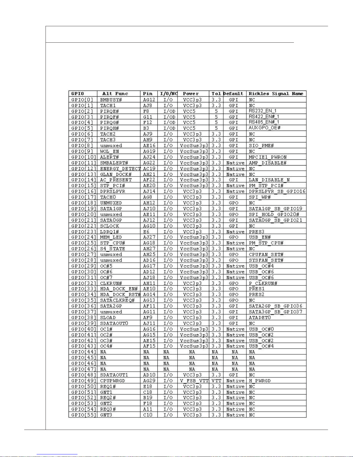
ICH8M GPIO
Page 56
4-7
MX255D
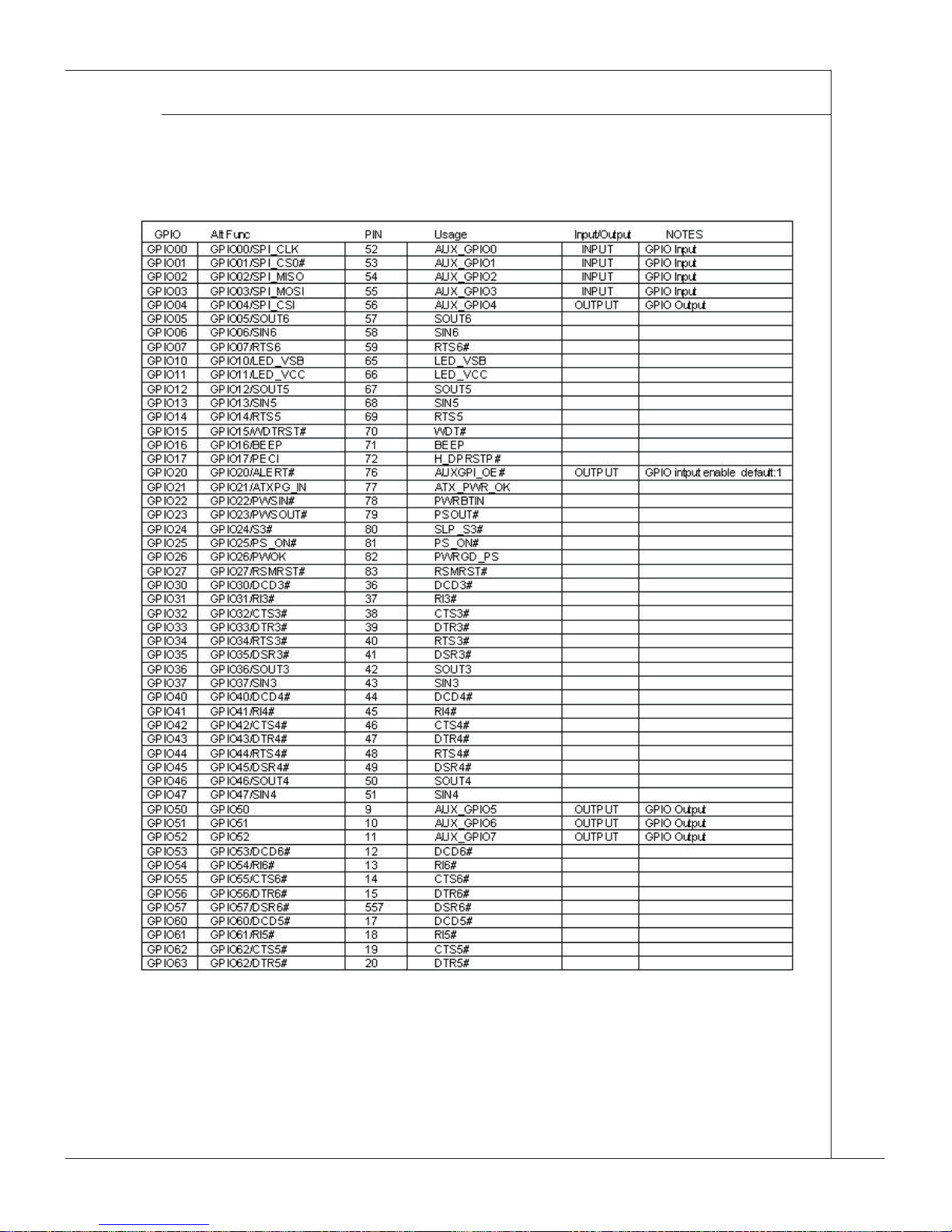
SIO GPIO
Page 57

4-8
▍ System Resources
GPIO Programming
GPIO Programming
Please refer to the “F81865 Super IO spec” for the GPIO pin function:
“Pin3-GPI00” Status:addr F2 bit0
“Pin4-GPO04” Status:addr F2 bit4, Setting:addr F1 bit4
“Pin5-GPI01” Status:addr F2 bit1
“Pin6-GPO50” Status:addr A2 bit0, Setting:addr A1 bit0
“Pin7-GPI02” Status:addr F2 bit2
“Pin8-GPO51” Status:addr A2 bit1, Setting:addr A1 bit1
“Pin9-GPI03” Status:addr F2 bit3
“Pin10-GPO52” Status:addr A2 bit2, Setting:addr A1 bit2
Note: GPIO pin connection design with 4 input and 4 output pins.
GPI is design for input, GPO is design for output
Example 1: Read data from GPIO “Pin3-GPI00”,
// the “Pin3-GPI00” status value is at address F2 bit 0,
Step 1. Enable SIO confi guration mode without timeout in between commands
Out(0x4e, 0x87); // (port, value), 0x4e for index
Out(0x4e, 0x87);
Step 2. Select LDN06 (GPIO) (LDN: Logic device number)
Out(0x4e, 0x07); // select entry page, 0x4e for index
Out(0x4f, 0x06); // select LDN06, 0x4f for data
Step 3. Set address to 0xF2
Out(0x4e, 0xF2); // 0x4e for index
Step 4. Get input data from port 0x4f
if (Inp(0x4f) & 0x01) !=0 ) // 0x4f for data, & 0x01 for bit0 of GPI00 input data
value = “high”;
else
value = “low”;
Page 58

4-9
MX255D
Example 2: Set GPIO “Pin4-GPO04” output to “high”,
// the “Pin4-GPO04” output setting is at address F1 bit 4,
Step 1. Enable SIO confi guration mode without timeout in between commands
Out(0x4e, 0x87); // (port, value), 0x4e for index
Out(0x4e, 0x87);
Step 2. Select LDN06 (GPIO) (LDN: Logic device number)
Out(0x4e, 0x07); // select entry page, 0x4e for index
Out(0x4f, 0x06); // select LDN06, 0x4f for data
Step 3. Set address to 0xF1
Out(0x4e, 0xF1); //0x4e for index
Step 4. Get data from port 0x4f (Save current state)
Byte tmp = Inp(0x4f); //Read current data for adding the output in bit4
Step 5. Write data to port 0x4f (only set bit 4 to “high” and write back)
Out(0x4f, tmp|0x10); //0x4f for data
Example 3: Set GPIO “Pin4-GPO04” output to “low”,
// the “Pin4-GPO04” output setting is at address F1 bit 4,
Step 1. Enable SIO confi guration mode without timeout in between commands
Out(0x4e, 0x87); // (port, value), 0x4e for index
Out(0x4e, 0x87);
Step 2. Select LDN06 (GPIO) (LDN: Logic device number)
Out(0x4e, 0x07); // select entry page, 0x4e for index
Out(0x4f, 0x06); // select LDN06, 0x4f for data
Step 3. Set address to 0xF1
Out(0x4e, 0xF1); //0x4e for index
Page 59

4-10
▍ System Resources
Step 4. Get data from port 0x4f (Save current state)
Byte tmp = Inp(0x4f); //Read current data for adding the output in bit4
Step 5. Write data to port 0x4f (only set bit 4 to “low” and write back)
Out(0x4f, tmp&0xEF);
 Loading...