

MX110H
Intel® H110
Mini ITX Motherboard supports 14nm Intel® Core™ i7/i5/i3
6
th
generation Desktop Processors (Skylake Pl at form)
User’sManual
Ver1.0

Safety Information
Electrical safety
To prevent electrical shock hazard, disconnect the power cable from the electrical outlet
before relocating the system.
When adding or removing devices to or from the system, ensure that the power cables
for the devices are unplugged before the signal cables are connected. If possible,
disconnect all power cables from the existing system before you add a device.
Before connecting or removing signal cables from the motherboard, ensure that all
power cables are unplugged.
Seek professional assistance before using an adapter or extension cord. These devices
could interrupt the grounding circuit.
Make sure that your power supply is set to the correct voltage in your area. If you are
not sure about the voltage of the electrical outlet you are using, contact your local power
company.
If the power supply is broken, do not try to fix it by yourself. Contact a qualified service
technician or your retailer.
Operation safety
Before installing the motherboard and adding devices on it, carefully read all the
manuals that came with the package.
Before using the product, make sure all cables are correctly connected and the power
cables are not damaged. If you detect any damage, contact your dealer immediately.
To avoid short circuits, keep paper clips, screws, and staples away from connectors,
slots, sockets and circuitry.
Avoid dust, humidity, and temperature extremes. Do not place the product in any area
where it may become wet.
Place the product on a stable surface.
If you encounter technical problems with the product, contact a qualified service
technician or your retailer.
T
he symbol of the crossed out wheeled bin indicates that the product
(electrical and electronic equipment) should not be placed in municipal
waste. Check local regulations for disposal of electronic products.

Safety Declaration
This device complies with the requirements in Part 15 of the FCC rules. Operation is subject to
the following two conditions:
This device may not cause harmful interference.
This device must accept any interference received, including interference that may
cause undesired operation.
About this guide
This user guide contains the information you need when installing and conf iguring the
motherboard.
How this guide is organized
This manual contains the following parts:
Section 1, 2: Product Introduction and Installation
This chapter describes the features of the motherboard and the new technology it
supports. This chapter also lists the hardware setup procedures that you have to
perform when installing system components. It includes description of the jumpers an d
connectors on the motherboard.
Section 3: BIOS setup
This chapter tells how to change system settings through the BIOS Setup menus.
Detailed descriptions of the BIOS parameters are also provided.
Where to find more information
Refer to the following sources for additional information and for product and software updates.
1. Motherboard User’s Manual and Device Drivers
Motherboard User’s Manual and Device Drivers can be downloaded at BCM Advanced
Research website: http://www.bcmcom.com/bcm_support_drivers.htm
2. Technical Support
If a problem arises with your system and no solution can be obtained from the user’s manual,
please contact your place of purchase or local distributor. Alternatively, ple ase try the following
help resources for further guidance. Visit the BCM Advanced Research website:
Revision History
Revision Revision
History
Date
V1.0 First release version
2016/07

4
Contents
1 Introduction ....................................................... 5
1.1 Package Contents ......................................................... 5
1.2 Speci cations ................................................................. 6
1.3 Motherboard Layout ....................................................... 9
1.4 I/O Panel ........................................................................ 11
2 Installation ......................................................... 12
2.1 Screw Holes ................................................................... 12
2.2 Pre-installation Precautions ........................................... 12
2.3 Processor ....................................................................... 13
2.3.1 Installing the CPU ................................................ 14
2.3.2 Installing the CPU Heatsink and Fan ................... 16
2.3.3 Uninstalling the CPU Heatsink and Fan ............... 18
2.4 Installation of Memory Modules (SO-DIMM) .................. 20
2.5 Expansion Slot ............................................................... 22
2.6 Jumpers Setup ............................................................... 23
2.7 Onboard Headers and Connectors ................................ 25
3 BIOS SETUP UTILITY ......................................... 30
3.1 Introduction .................................................................... 30
3.1.1 BIOS Menu Bar .................................................... 30
3.1.2 Navigation Keys ................................................... 31
3.2 Main Screen ................................................................... 31
3.3 Advanced Screen ........................................................... 32
3.3.1 CPU Configuration ............................................... 33
3.3.2 Chipset Confi
guration........................................... 35
3.3.3 Storage Configuration .......................................... 37
3.3.4 Super IO Configuration ........................................ 38
3.3.5 ACPI Confi
guration............................................... 39
3.3.6 USB Confi
guration ............................................... 40
3.3.7 Trusted Computing (optional)............................... 41
3.4 Hardware Health Event Monitoring Screen ................... 42
3.5 Security Screen ............................................................. 43
3.6 Boot Screen ................................................................... 44
3.7 Exit Screen .................................................................... 46
4 Appendix............................................................................ 47

5
Chapter 1: Introduction
Thank you for purchasing MX110H motherboard, a reliable motherboard produced
under our consistently stringent quality control. It delivers excellent performance
with robust design conforming to our commitment to quality and endurance.
Because the motherboard specifications and the BIOS software might be
updated, the content of this manual will be subject to change without no-
tice. In case any modifi
cations of this manual occur, the updated
version will be available on our website without further notice.
If you require technical support related to this motherboard, please visit
our website for specific information about the model you are using.
1.1 Package Contents
MX110H Motherboard (Mini-ITX Form Factor: 6.7-in x 6.7-in)
MX110H 1 x I/O Panel Shield
6
1.2 Specifi cations
Model Name MX110H
MB Dimension
Mini-ITX 6.7 x 6.7 inches
8 Layer Board
BCM Standard Blue
CAP All Solid CAP
Fanless
No
ATX PWR IN
System
CPU
Chipsets
(PCH)
System
Memory
Display
Ethernet
Audio
Super I/O
Expansion
Interface
Intel
®
Skylake Processor
Supports LGA 1151 Core i7, Core i5, Core i3, Celeron
CPU Up to 65W Max
Intel
®
H110
6 x PCIex1 Channel Available
2 x SoDIMM Up to 32GB Dual Channel DDR4 2133Mhz
Vertical Type Memory Sockets
Intel
®
Integrated HD Graphic (CPU Dependent)
2 x DisplayPort
18/24 bits Dual Channel LVDS Through Chrontel®
CH7511B (BOM option to support eDP)
2 GigaLan support
Intel® i219-V PHY LAN Controller
Intel® i211-AT PCIe LAN Controller
Realtek®ALC887
ALC122, 3W Per Channel Amplier
Nuvoton® NCT6106D
1 x RS232/422/485 port (with 5V/12V/RI set by jumper)
1x RS-232 (with 5V/12V/RI set by Jumper)
2x RS-232 (with 5V/12V set by Jumper)
1 x PCIe x 16 Slot (From CPU)
1 x Full/Half Size Mini-PCIe with mSATA Support (SATA
III) (+USB)
1 x Half Size Mini-PCIe (+USB)
Note: Two sockets can be placed in stack
Watch Dog
Timer (WDT)
1 ~ 255 sec timer
RTC
BIOS
Others
Date and Time
AMI® UEFI BIOS
16MB (128Mb) Flash ROM
TPM 2.0 (Optional) IC on-board design

7
Internal I/O
Display
1 x LVDS/eDP shared Header
1 x Backlight Locking Type Header
Storage
3 x SATA III Connectors (Red)
1 x SATA III Connectors (Shared with mSATA) (Black)
USB
1 x USB 2.0 2.54mm Headers (2 Ports Total)
1 x USB 3.0 Header with Shroud (2 Ports Total)
Audio
1 x Front Audio Header (2.54mm Pitch)
1 x Amplifer Locking Type Header (2.00mm Pitch)
Serial Port
2 x RS-232 2.0mm Locking Type Headers (with Voltage
Selection)
Note: 5V/12V/RI, set by Jumper
Parallel Port 1 x LPT Header with Shroud (2.0mm Pitch)
Digital I/O 1 x 8 bits GPIO Header
Battery Cable Type CMOS Battery
FAN
1 x 4 Pin CPU Fan Header
1 x 4 Pin Chassis Fan Header
Power In
1 x Standard 24 pin ATX Connector
1 x 4 pin ATX 12 Connector
Front Panel 1 x Front Panel Header (2.54mm Pitch)
LPC Header 1 x LPC Header (2.0mm Pitch)
CI (Chassis
Intrusion)
2 x Chassis Intrusion Locking Type Headers
Others
1 x SPI Header (2.0mm Pitch)
1 x AT/ATX Mode Jumper
Rear I/O
Keyboard/
Mouse (PS/2)
2 x PS/2
Serial Port
2 x DB-9 Connector
1 port with RS-232/422/485 support
1 port just only support RS-232
Both with 5V/12V/RI suport at Pin9
Note: 5V/12V/RI, set by Jumper; RS232/422/485 set by
BIOS
LAN 2 x RJ45 (stack with USB)
USB2.0 2 x USB 2.0 (stack with RJ45)
USB 3.0 2 x USB 3.0 (stack with RJ45)
Display 2 x DP Connectors
Audio 1 x 3 Jacks Audio Connector (30mm Height)
8
Others
Regulatory
Compliance
Design to Comply with FCC/CE/UL
Operation
Environment
Storage
Environment
RoHS Compliant
Temperature: 0 C to 60 C Note:In environment of
45C or above, it requires active system fan cooling
Temperature: -20 C to 60 C
Humidity: 5% to 90% non-condensing
Accessories 1 x I/O Shield
9
1.3 Motherboard Layout
COM3
1
COM4
1
LVDS1
1
mini PCIe
BUZZ1
BIOS
Chip
SPEAKER1
1
PCIE1
1
LPC1
1
HD_AUDIO1
ATX12V1
CPU_FAN1
CHA_FAN1
1
LPT1
USB3_34
1
SPI1
CLRMOS1
1
HDLED RESET
PLED PWRBTN
PANEL1
1
SATA3_2
1
USB2_34
1
BLT_PWR1
BLT_PWM1
1
CI2
1
CI1
1
1
JGPIO1
11
8
10
16
14
20
19
22
24
26
COM2
PS2
Keyboard
PS2
Mouse
COM1
DISPLAY1
DISPLAY2
Top:
RJ-45
USB 3.0
T:USB1
B: USB2
Top:
RJ-45
USB 2.0
T:USB1
B: USB2
Top:
LINE IN
Center:
FRONT
Bottom:
MIC IN
Intel
H110
SATA3_4
SATA3_1
SATA3_3
ATXPWR1
DDR4_B1
DDR4_A1
1
PWR_COM2
1
PWR_COM1
mini PCIe/ mSATA
PWR_JP1
1
JGPIO_PWR1
1
JGPIO_SET1
MSATA_SEL1
PWR_COM4
PWR_COM3
1
1
1
1

10
1 : ATX/AT Mode Select
2 : Digital Input/Output Power Select
3
: GPIO Default Setting
4 : mSATA Select
5 : COM Port PWR Setting Jumpers
PWR_COM3 (For COM Port3)
PWR_COM4 (For COM Port4)
6 :
USB3.0 Header
7 : Printer Port Header
8 :
USB2.0 Header
9 : LPC Header
10 : Digital Input/Output Pin Header
11 : 24-pin ATX Power Input Connector
12 : Clear CMOS Header
13 :
4-Pin CPU FAN Connector (+12V)
14 :
4-Pin Chassis FAN Connector (+12V)
15 :
System Panel Header
16 : 3W Audio AMP Output Wafer
17 : 4-pin ATX Power Input Connector
18 : SPI Connector
19 :
Front Panel Audio Header
20 : SATA3 Connectors (SATA3_1, SATA3_2, SATA3_3, SATA3_4)
21 : Inverter Power Control Wafer (BLT_PWR1)
22 : Backlight Control Level (BLT_PWM1)
23 :
Chassis Intrusion Headers
24 :
LVDS Panel Connector
25 : COM Port PWR Setting Jumpers
PWR_COM1 (For COM Port1)
PWR_COM2 (For COM Port2)
26 : COM3, 4 Headers (RS232)
11
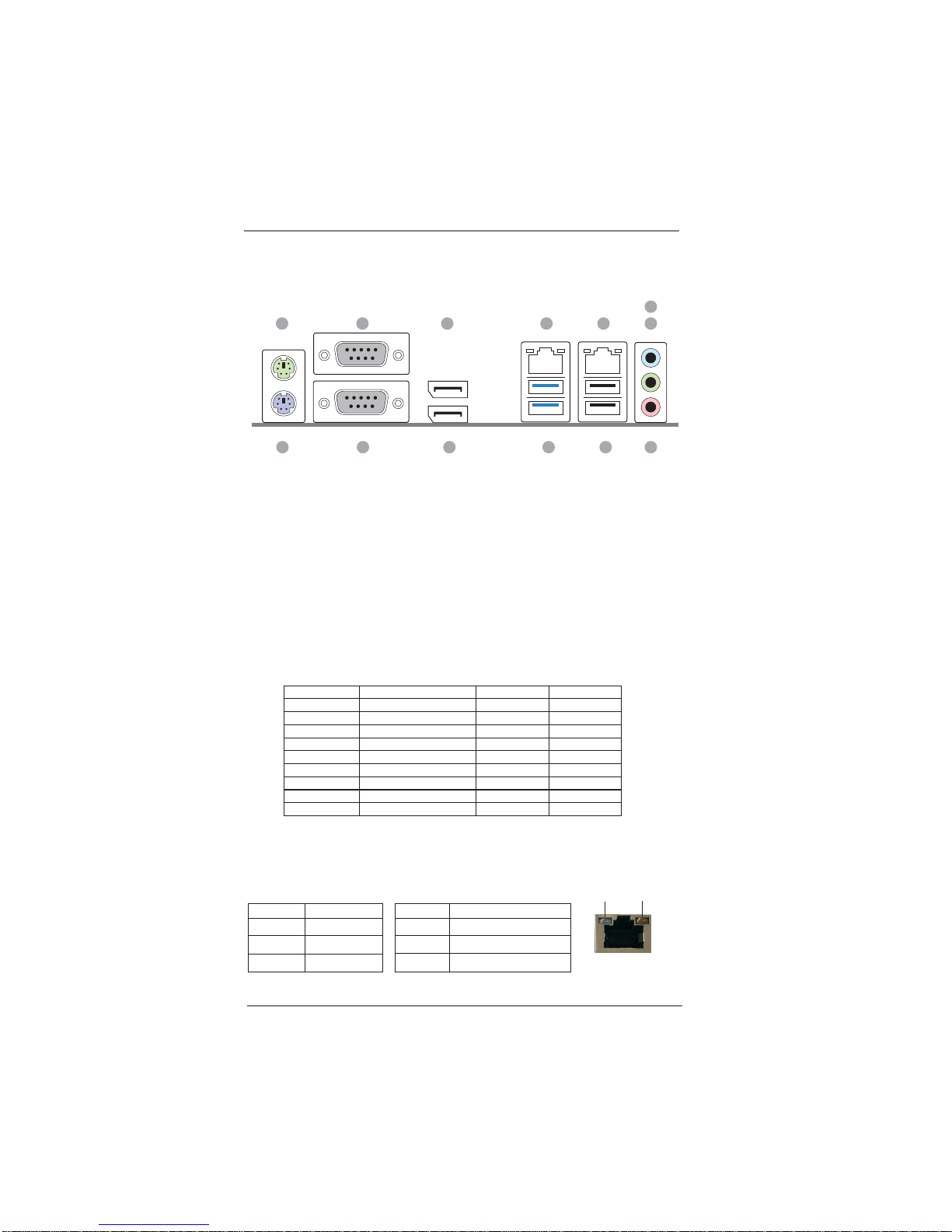
1.4 I/O Panel
** There are two LED next to the LAN port. Please refer to the table below for the LAN port LED
indications.
LAN Port LED Indications
Activity/Link LED SPEED LED
Status Description Status Description
Off No Link Off 10Mbps connection
Blinking Data Activity Green 100Mbps connection
On Link Orange 1Gbps connection
1 PS/2 Mouse Port
2 COM Port (COM1)*
3 DisplayPort (DP1)
4 LAN RJ-45 Port (LAN1)**
5 LAN RJ-45 Port (LAN2)**
6 Line In (Light Blue)
7 Front Speaker (Lime)
8 Microphone (Pink)
9 USB 2.0 Ports (USB_12)
10 USB 3.0 Ports (USB3_12)
11 DisplayPort (DP2)
12 COM Port (COM2)
13 PS/2 Keyboard Port
ACT/LINK
LED
SPEED
LED
LAN Port
13 8911
12
7
6
1 5
10
42 3
PIN RS232 RS422 RS485
1 DCD TX- RTX2 RXD RX+ N/A
3 TXD TX+ RTX+
4 DTR RX- N/A
5 GND GND GND
6 DSR N/A N/A
7 RTS N/A N/A
8 CTS N/A N/A
9 RI# / +5V / +12V N/A N/A
*
This motherboard supports RS232/422/485 on COM1 port. Please refer to below table for the
pin de nition. In addition, COM1 port (RS232/422/485) can be adjusted in BIOS setup utility >
Advanced Screen > Super IO Confi
guration. You may refer to page 38 for details.
COM1 Port Pin Defi nition

12
Chapter 2: Installation
This is a Mini-ITX form factor (6.7" x 6.7", 17.0 x 17.0 cm) motherboard. Before
you install the motherboard, study the configuration of your chassis to ensure
that the motherboard fi
ts into it.
Make sure to unplug the power cord before installing or removing the
motherboard. Failure to do so may cause physical injuries to you and
damages to motherboard components.
2.1 Screw Holes
Place screws into the holes to secure the motherboard to the chassis.
Do not over-tighten the screws! Doing so may damage the motherboard.
2.2 Pre-installation Precautions
Take note of the following precautions before you install motherboard components
or change any motherboard settings.
1. Unplug the power cord from the wall socket before touching any component.
2. To avoid damaging the motherboard components due to static electricity,
NEVER place your motherboard directly on the carpet or the like. Also
remember to use a grounded wrist strap or touch a safety grounded object
before you handle components.
3. Hold components by the edges and do not touch the ICs.
4. Whenever you uninstall any component, place it on a grounded antistatic pad or
in the bag that comes with the component.
Before you install or remove any component, ensure that the power is
switched off or the power cord is detached from the power supply.
Failure to do so may cause severe damage to the motherboard, peripherals,
and/or components.

13
2.3 Processor
The board supports 6th generation Intel Core processors. Other processors may be
supported in the future. This board supports processors with a maximum wattage of
65 W Thermal Design Power (TDP).
NOTE
This board has specific requirements for providing power to the processor.Additional
power required will depend on configurations chosen by the integrator.
The motherboard comes with a surface mount LGA1151 socket designed for the Intel® Core™
i7/ i5/ i3 processor in the 1151-land package.
z
Your boxed Intel® Core™ i7/ i5/ i3 LGA1151 processor package
should come with installation instructions for the CPU, fan and
heatsink assembly. If the instructions in this section do not match the
CPU documentation, follow the latter.
z Upon purchase of the motherboard, make sure that the PnP cap is on
the socket and the socket pins are not bent. Contact your retailer
immediately if the PnP cap is missing, or if you see any damage to
the PnP cap/socket pins/motherboard components. BCM will shoulder
the cost of repair only if the damage is shipment/transit-related.
z Keep the cap after installing the motherboard. BCM will process
Return Merchandise Authorization (RMA) requests only if the
motherboard comes with the cap on the LGA1151 socket.
z The product warranty does not cover damage to the socket pins
resulting from incorrect CPU installation/removal, or
misplacement/loss/incorrect removal of the PnP cap.
z Install the CPU fan and heatsink assembly before you install
motherboard to the chassis.
If
you purchased a separate CPU heatsink and fan assembly, make sure
that you have properly applied Thermal Interface Material to the CPU
heatsink or CPU before you install the heatsink and fan assembly.
14
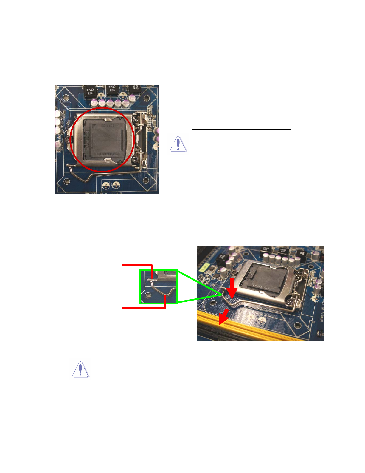
2.3.1 Installing the CPU
1. Locate the CPU socket on the motherboard.
2.
Remove the PnP cap.
3. Press the load lever with your thumb (A), then move it to the left (B) until it is released
from the retention tab.
To prevent damage to the socket pins, do not remove the PnP cap unless
you are installing a CPU.
Before installing the CPU, make
sure that the socket box is facing
towards you and the load lever is
on your left.
A
B
Retentiontab
Loadlever
15
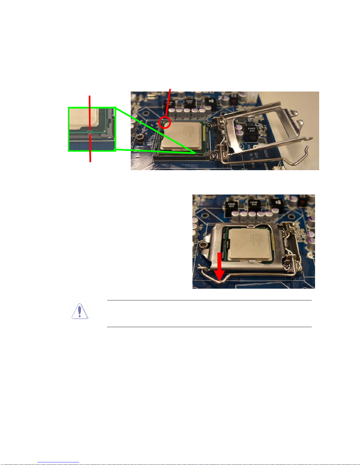
4. Position the CPU over the socket, making sure that the gold triangle is on the top-left corner
of the
socket then fit the socket alignment key into the CPU notch.
5. Pull back the load lever, then push the load
lever (A) until it snaps into the retention tab.
The C
PU fits in only one correct orientation. DO NOT force the CPU into
the socket to prevent bending the connectors on the socket and damaging
the CPU!
Alignmentkey
CPUnotch
Goldtriangle
A
16
2.3.2 Installing the CPU Heatsink and Fan
Intel®Core™i7/i5/i3LGA1151processorrequiresaspeciallydesignedheatsinkandfanassemblyto
ensureoptimumthermalconditionandperformance.
z I
nstall the motherboard to the chassis before you install the CPU fan
and heatsink assembly.
z When you buy a boxed Intel® Core™ i7/ i5/ i3 LGA1151 processor, the
package includes the CPU fan and heatsink assembly. If you buy a
CPU separately, make sure that you use only Intel® certified multi‑
directional heatsink and fan.
z Your Intel® Core™ i7/ i5/ i3 LGA1151 processor heatsink and fan
assembly comes in a push-pin design and requires no tool to install.
If
you purchased a separate CPU heatsink and fan assembly, make
sure that you have properly applied Thermal Interface Material to the
CPU heatsink or CPU before you install the heatsink and fan assembly.
To install
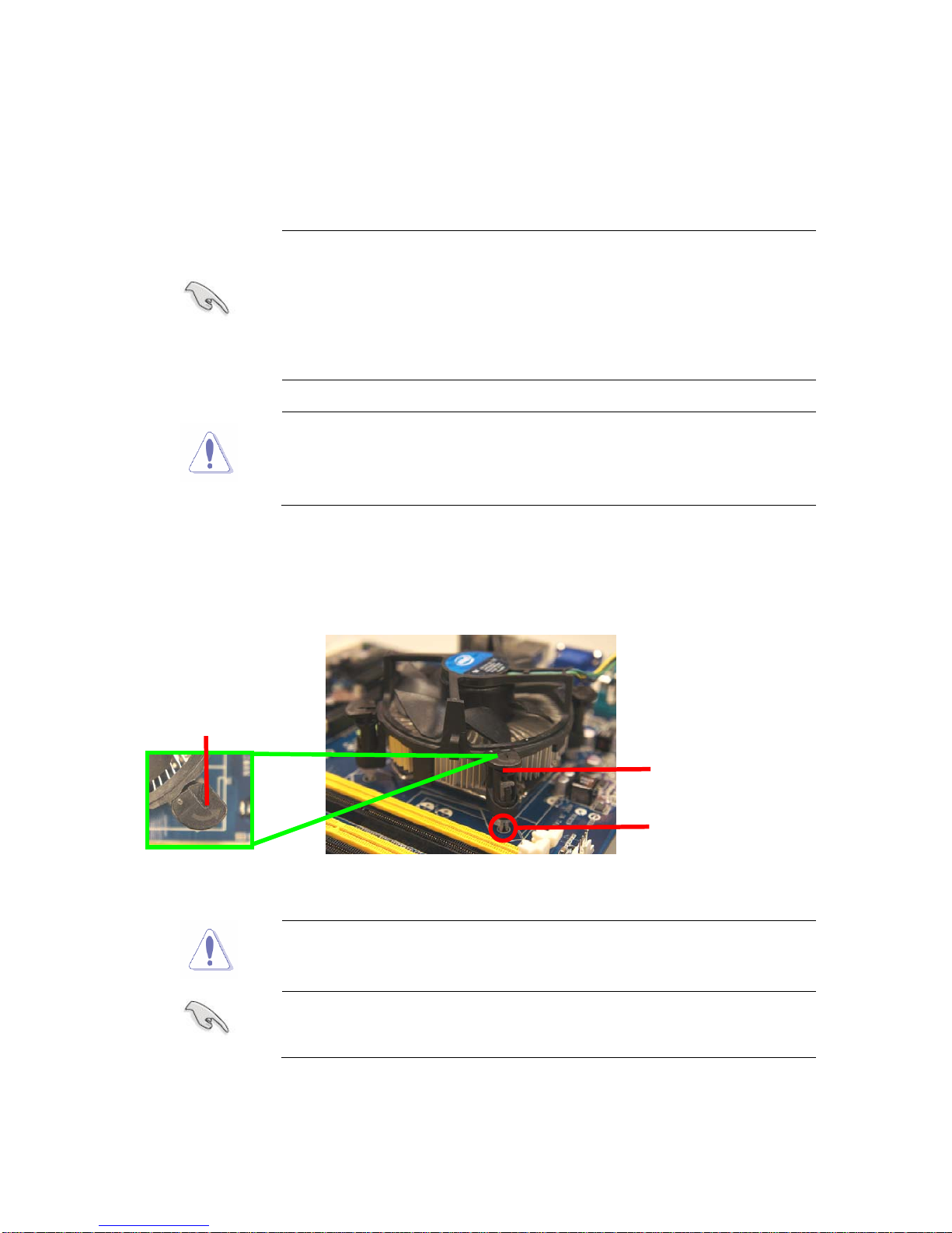
the CPU heatsink and fan:
1. Plac
e the heatsink on top of the installed CPU, making sure that the four fasteners ma
tch
the holes on the motherboard.
Orient the heatsink and fan assembly such that the CPU fan cable is
closest to the CPU fan connector.
z M
ake sure each fastener is oriented as shown, with the narrow
groove directed outward.
Motherboardhole
Fastener
Narrowend
thegroove
17
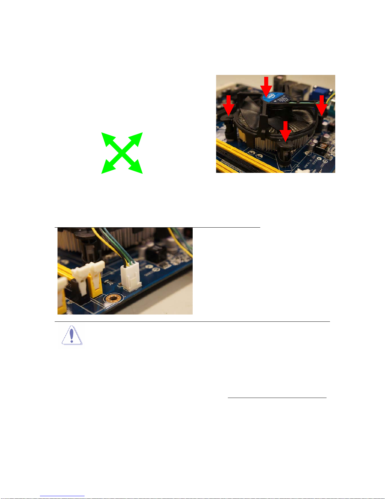
2. Pus
h down two fasteners at a time in a diagon
al
s
equence to secure the heatsink and fan assembly in
place.
3. Co
nnect the CPU fan cable to the connector on the motherboard la
beled CPU_FAN.
Do no
t forget to connect the fan
cables to the fan connectors.
Insufficient air flow inside the
system may damage the
motherboardcomponents.
These are not jumpers! DO NOT
place jumper caps on the fan
connectors.
A
A
B
B
A
B
A
B

18
2.3.3UninstallingtheCPUHeatsinkandFan
TouninstalltheCPUheatsinkandfan:
1. DisconnecttheCPUfancablefromtheconnectoronthemotherboard.
2. Rotateeachfastenercounterclockwise
3.
Pull up two fasteners at a time in a diagonal sequence to disengage the heatsink and fan
assembly from the motherboard.
A
B
A
B
A
A
B
B

19
4. Ca
refully remove the heatsink and fan
assembly from the motherboard.
5. Rotate each fastener clockwise to ensure
correct orientation when reinstalling.

20
2.4 Installation of Memory Modules (SO-DIMM)
MX110H motherboard provides two DDR4 (Double Data Rate 4) SO-DIMM slots,
which support Dual Channel DDR4.
1. It is not allowed to install a DDR, DDR2 or DDR3 memory module into
a DDR4 slot; otherwise, this motherboard and SO-DIMM may be
damaged.
2. Please make sure to disconnect the power supply before adding or
removing SO-DIMMs or the system components.
3.
The SO-DIMM only
fits in one correct orientation. It will cause
permanent damage to the motherboard and the SO-DIMM if you force
the SO-DIMM into the slot at incorrect orientation.

21
1
2
3

22
2.5 Expansion Slots (mini-PCIe, mini-PCIe / mini-SATA and
PCI Express Slots)
There is 1 mini-PCIe slot, 1 mini-PCIe / mini-SATA slot and 1 PCI Express slot on
this motherboard.
mini-PCIe slot:
MINI_PCIE1 (mini-PCIe slot; half size) is used for PCI Express mini
cards.
mini-PCIe / mini-SATA slot:
MINI_SATA1 (mini-PCIe / mini-SATA slot; full size) is used for mSATA
cards.
PCIE slot: PCIE1 (PCIE x16 slot) is used for PCI Express x16 lane width cards.
Installing an expansion card
Step 1. Before installing the expansion card, please make sure that the power
Step 2.
Step 3.
Step 4.
Step 5.
Step 6.
supply is switched off or the power cord is unplugged. Please read the
documentation of the expansion card and make necessary hardware
settings for the card before you start the installation.
Remove the system unit cover (if your motherboard is already installed
in a chassis).
Remove the brac
ket facing the slot that you intend to use. Keep the
screws for later use.
Align the card connector with the slot and press firmly until the card is
completely seated on the slot.
Fasten the card to the chassis with screws.
Replace the system cover.

23
2.6 Jumpers Setup
The illustration shows how jumpers are
setup. When the jumper cap is placed on
pins, the jumper is “Short”. If no jumper cap
is placed on pins, the jumper is “Open”. The
illustration shows a 3-pin jumper whose
pin1 and pin2 are “Short” when jumper cap
is placed on these 2 pins.
Clear CMOS Jumper
(CLRCMOS1)
(see p.9, No. 12)
Note: CLRCMOS1 allows you to clear the data in CMOS. To clear and reset the
system parameters to default setup, please turn off the computer and unplug
the power cord from the power supply. After waiting for 15 seconds, use a
jumper cap to short pin2 and pin3 on CLRCMOS1 for 5 seconds. However,
please do not clear the CMOS right after you update the BIOS. If you need
to clear the CMOS when you just finish updating the
BIOS, you must boot up
the system first, and then shut it down before you do the clear-CMOS action.
Please be noted that the password, date, time, user default profile will be
cleared only if the CMOS battery is removed.
Clear CMOSDefault
Digital Input / Output Power Select
1-2: +12V
(3-pin JGPIO_PWR1)
2-3: +5V (Default)
(see p.9 No. 2)
ATX/AT Mode Select
1-2: AT Mode
(3-pin PWR_JP1)
2-3: ATX Mode (Default)
(see p.9 No. 1)
Backlight Control Level
(CON_LBKLT_CTL)
1-2: +3V
(3-pin BLT_PWM1)
2-3: +5V (Default)
(see p.9, No. 22)
GPIO Default Setting
1-2: Pull-High (Default)
(3-pin JGPIO_SET1)
2-3: Pull-Low
(see p.9 No. 3)

24
COM Port Pin9 PWR Setting Jumpers 1-2: +12V
(6-pin PWR_COM1, for COM Port1)
3-4: RI# (Default)
(6-pin PWR_COM2, for COM Port2)
5-6: +5V
(see p.9, No. 5)
(3-pin PWR_COM3, for COM Port3)
1-2: +5V (Default)
(3-pin PWR_COM4, for COM Port4)
2-3: +12V
(see p.9, No. 5)
mSATA Select
1-2:
Mini-PCIE + SATA3_4 (Default)
(3-pin MSATA_SEL1)
2-3:
mSATA (no SATA3_4)
(see p.9 No. 4)

25
2.7 Onboard Headers and Connectors
Onboard headers and connectors are NOT jumpers. Do NOT place
jumper caps over these headers and connectors. Placing jumper caps
over the headers and connectors will cause permanent damage of the
motherboard!
SATA3 Connectors These four Serial ATA3
(SATA3_1: see p.9, No. 20)
(SATA3) connectors support
(SATA3_2: see p.9, No. 20)
SATA data cables for internal
(SATA3_3: see p.9, No. 20)
storage devices. The current
(SATA3_4: see p.9, No. 20)
SATA3 interface allows up to
6.0 Gb/s data transfer rate.
USB 2.0 Connector There is one USB 2.0
(9-pin USB2_34)
connector on this
(see p.9 No. 8)
motherboard. This USB 2.0
connector can support two USB
ports.
System Panel Header This header accommodates
(9-pin PANEL1)
several system front panel
(see p.9 No. 15)
functions.
Connect the power switch, reset switch and system status indicator on the
chassis to this header according to the pin assignments below. Note the
positive and negative pins before connecting the cables.
PWRBTN (Power Switch):
Connect to the power switch on the chassis front panel. You may confi
gure
the way to turn off your system using the power switch.
RESET (Reset Switch):
Connect to the reset switch on the chassis front panel. Press the reset
switch to restart the computer if the computer freezes and fails to perform a
normal restart.
PLED (System Power LED):
Connect to the power status indicator on the chassis front panel. The LED
is on when the system is operating. The LED keeps blinking when the sys-
tem is in S1 sleep state. The LED is off when the system is in S3/S4 sleep
state or powered off (S5).
SATA3_2
SATA3_1
SATA3_4
SATA3_3
NC
GND
RESET#
PWRBTN#
PLED-
PLED+
GND
HDLED-
HDLED+
1
GND

26
HDLED (Hard Drive Activity LED):
Connect to the hard drive activity LED on the chassis front panel. The LED
is on when the hard drive is reading or writing data.
The front panel design may differ by chassis. A front panel module mainly
consists of power switch, reset switch, power LED, hard drive activity LED,
speaker and etc. When connecting your chassis front panel module to this
header, make sure the wire assignments and the pin assign-ments are
matched correctly.
3W Audio AMP Output Wafer
(4-pin SPEAKER1)
(see p.9 No. 16)
Front Panel Audio Header This is an interface for front
(9-pin HD_AUDIO1)
panel audio cable that allows
(see p.9 No. 19)
convenient connection and
control of audio devices.
1.
High Defi
nition Audio supports Jack Sensing, but the panel wire on
the chassis must support HDA to function correctly. Please follow the
instruction in our manual and chassis manual to install your system.
2. If you use AC’97 audio panel, please install it to the front panel audio
header as below:
A. Connect Mic_IN (MIC) to MIC2_L.
B. Connect Audio_R (RIN) to OUT2_R and Audio_L (LIN) to OUT2_L.
C. Connect Ground (GND) to Ground (GND).
D. MIC_RET and OUT_RET are for HD audio panel only. You don’t
need to connect them for AC’97 audio panel.
E. To activate the front mic.
Go to the “FrontMic” Tab in the Realtek Control panel. Adjust
“Recording Volume”.
Chassis Fan Connector Please connect the fan cable
(4-pin CHA_FAN1)
to the fan connector and
(see p.9 No. 14)
match the black wire to the
ground pin.
PIN Signal Name
1 OUTLN
2 OUTLP
3 OUTRP
4 OUTRN
1
J_SENSE
OUT2_L
MIC_RET
PRESENCE#
GND
OUT2_R
MIC2_R
MIC2_L
OUT_RET
1
FAN_SPEED
FAN_SPEED_CONTROL
+12V
GND

27
Though this motherboard provides 4-Pin CPU fan (Quiet Fan) support, the 3-Pin
CPU fan still can work successfully even without the fan speed control function.
If you plan to connect the 3-Pin CPU fan to the CPU fan connector on this
motherboard, please connect it to Pin 1-3.
3-Pin Fan Installation
Pin 1-3 Connected
ATX Power Input Connector Please connect a DC
(Input 12V) 12V power supply to this
(4-pin ATX12V1)
connector.
(see p.9 No. 17)
1-2: GND
3-4: DC Input
CPU Fan Connector Please connect the CPU fan
(4-pin CPU_FAN1)
cable to the connector and
(see p.9 No. 13)
match the black wire to the
ground pin.
4
2
3
1
Printer Port Header
(25-pin LPT1)
(see p.9 No. 7)
LVDS Connector
(40-pin LVDS1)
(see p.9 No. 24)
1
AFD#
ERROR#
PINIT#
GND
SLIN#
STB#
SPD0
SPD1
SPD2
SPD3
SPD4
SPD5
SPD6
SPD7
ACK#
BUSY
PE
SLCT
PIN Signal Name PIN Signal Name
2 VDD_+5V 1 VDD_+3.3V
4 VDD_+5V 3 VDD_+3.3V
6 DDC_DATA 5 DDC_CLK
8 GND 7 GND
10 LVDS_A0+ 9 LVDS_A1+
12 LVDS_A0- 11 LVDS_A1-
14 GND 13 GND
16 LVDS_A2+ 15 LVDS_A3+
18 LVDS_A2- 17 LVDS_A3-
20 GND 19 GND
22 LVDS_B0+ 21 LVDS_B1+
24 LVDS_B0- 23 LVDS_B1-
26 GND 25 GND
28 LVDS_B2+ 27 LVDS_B3+
30 LVDS_B2- 29 LVDS_B3-
32 GND 31 GND
34 LVDS_A_CLK+ 33 LVDS_B_CLK+
36 LVDS_A_CLK- 35 LVDS_B_CLK-
38 GND 37 GND
40 VDD_+12V 39 VDD_+12V
1
39
40
2
GND
+12V
CPU_FAN_SPEED
FAN_SPEED_CONTROL

28
Chassis Intrusion Headers This motherboard supports
(2-pin CI1, CI2: see p.9, No. 23)
CASE OPEN detection feature
that detects if the chassis cover
has been removed. This feature
requires a chassis with chassis
intrusion detection design.
COM3, 4 Headers (RS232)
(9-pin COM3/COM4: see p.9, No. 26)
LPC Header
(19-pin LPC1)
(
see p.9, No. 9)
1
Signal
GND
1
GND
GND
S_PWRDWN#
LAD2
SMB_CLK_MAIN
PCICLK
PCIRST#
LAD3
+3V
LAD0
GND
FRAME
SMB_DATA_MAIN
LAD1
SERIRQ#
GND
+3VSB
48MHz
+5V
USB 3.0 Connector There is one USB 3.0
(9-pin USB3_34)
connector on this
(see p.9 No. 6)
motherboard. This USB 3.0
connector can support two USB
ports.
1
ID
IntA_P_D+
IntA_P_D-
GND
IntA_P_SSTX+
IntA_P_SSTX-
GND
IntA_P_SSRX+
Vbus
IntA_P_D+
IntA_P_D-
GND
IntA_P_SSTX+
IntA_P_SSTX-
GND
IntA_P_SSRX+
IntA_P_SSRX-
Vbus
IntA_P_SSRX-
SPI Connector
(7-pin SPI1: see p.9, No. 18)
PIN
Signal
Name
PIN
Signal
Name
PIN
Signal
Name
PIN Signal Name
7
GND
5
CLK
3 SPI_MOSI 1
NC
8 +3.3V 6 SPI_CS# 4 SPI_MISO 2 SPI_HOLD1#
PIN Signal Name PIN Signal Name
1 DDCD# 2
RRXD
3
TTXD
4 DDTR#
5
GND
6
DDSR#
7
RRTS#
8
CCTS#
9 +5V / +12V 10 NC
21
For Update EEPROM BIOS
purpose only

29
Digital Input/Output Pin Header
(12-pin JGPIO1: see p.9, No. 10)
Inverter Power Control Wafer
(5-pin BLT_PWR1: see p.9, No. 21)
PIN Signal Name
1 +12_BL
2 GND
3 CON_LBKLT_EN
4 CON_LBKLT_CTL
5 +5V_BL
1
PIN
Signal
Name
PIN
Signal
Name
PIN
Signal
Name
PIN
Signal
Name
PIN Signal Name PIN Signal Name
2
SIO_GP20 4 SIO_GP21 6 SIO_GP22 8 SIO_GP23 10 SMB_DATA 12 GND
1 SIO_GP24 3 SIO_GP25 5 SIO_GP26 7 SIO_GP27 9 SMB_CLK 11 JGPIO_PWR
ATX Power Input Connector Please connect a power supply
(24-pin ATXPWR1)
to this connector.
(see p.9 No. 11)
24 13
12 1

30
Chapter 3: BIOS SETUP UTILITY
3.1 Introduction
This section explains how to use the BIOS SETUP UTILITY to configure your
system. The Bios chip on the motherboard stores the
BIOS SETUP UTILITY. You
may run the BIOSSETUP UTILITY when you start up the computer. Please press
<F2> or <Del> during the Power-On-Self-Test (POST) to enter the BIOS
SETUP UTILITY, otherwise, POST will continue with its test routines.
If you wish to enter the BIOS SETUP UTILITY after POST, restart the system
by pressing <Ctl> + <Alt> + <Delete>, or by pressing the reset button on the
system chassis. You may also restart by turning the system off and then back on.
Because the BIOS software is
often being updated, the
following BIOS setup screens and descriptions are for
reference purpose only, and they may not exactly match what
you see on your screen.
3.1.1 BIOS Menu Bar
The top of the screen has a menu bar with the following selections:
Main To set up the system time/date information
Advanced To set up the advanced BIOS features
H/W Monitor To display current hardware status
Security To set up the security features
Boot To set up the default system device to locate and load the
Operating System
Exit
To exit the current screen or the BIOS SETUP UTILITY
Use < > key or < > key to choose among the selections on the menu
bar, and then press <Enter> to get into the sub screen. You can also use the
mouse to click your required item.

31
3.1.2 Navigation Keys
Please check the following table for the function description of each navigation
key.
Navigation Key(s) Function Description
/ Moves cursor left or right to select Screens
/ Moves cursor up or down to select items
+ / - To change option for the selected items
<Enter> To bring up the selected screen
<F1> To display the General Help Screen
<F7> Discard changes
<F9> To load optimal default values for all the settings
<F10> To save changes and exit the UEFI SETUP UTILITY
<F12> Print screen
<ESC> To jump to the Exit Screen or exit the current screen
3.2 Main Screen
When you enter the BIOS SETUP UTILITY, the Main screen will appear and
display the system overview.

32
Setting wrong values in this section may cause
the system to malfunction.
3.3 Advanced Screen
In this section, you may set the configurations for the following items: CPU
Configuration, Chipset Configuration, Storage Configuration, Super IO
Con
figuration, ACPI Configuration, and USB Configuration.

33
3.3.1 CPU Confi guration
Please note that enabling this function may reduce CPU voltage and lead to system
stability or compatibility issues with some power supplies. Please set this item to
[Disabled] if above issues occur.
Active Processor Cores
Use this item to select the number of cores to enable in each processor
package. The default value is [All].
CPU C States Support
Enable CPU C States Support for power saving. It is recommended to
keep C3, C6 and C7 all enabled for better power saving.
Enhanced Halt State (C1E)
Enable Enhanced Halt State (C1E) for lower power consumption.
CPU C3 State Support
Use this to enable or disable CPU C3 (ACPI C2) report to OS.
CPU C6 State Support
Use this to enable or disable CPU C6 (ACPI C3) report to OS.
CPU C7 State Support
Use this to enable or disable CPU C7 (ACPI C7) report to OS.
Package C State Support
Selected option will program into C State package limit register. The
default value is [Auto].
Intel SpeedStep Technology
Intel SpeedStep technology is Intel’s new power saving technology. Pro-
cessors can switch between multiple frequencies and voltage points to en-
able power saving. The default value is [Enabled]. Confi
guration options:
[Enabled] and [Disabled]. If you install Windows® 8 / 8.1 and want to en-
able this function, please set this item to [Enabled]. This item will be hid-
den if the current CPU does not support Intel SpeedStep technology.

34
Intel Turbo Boost Technology
Intel Turbo Boost Technology enables the processor to run above its base
operating frequency when the operating system requests the highest
performance state.
CPU Thermal Throttling
You may select [Enabled] to enable CPU internal thermal control
mechanism to keep the CPU from overheating.
No-Execute Memory Protection
No-Execution (NX) Memory Protection Technology is an enhancement
to the IA-32 Intel Architecture. An IA-32 processor with “No Execute (NX)
Memory Protection” can prevent data pages from being used by malicious
software to execute codes. This option will be hidden if the current CPU
does not support No-Excute Memory Protection.
Intel Virtualization Technology
When this option is set to [Enabled], a VMM (Virtual Machine Architecture)
can utilize the additional hardware capabilities provided by Vanderpool
Technology. This option will be hidden if the installed CPU does not
support Intel Virtualization Technology.
Hardware Prefetcher
Use this item to turn on/off the MLC streamer prefetcher.
Adjacent Cache Line Prefetch
Use this item to turn on/off prefetching of adjacent cache lines.

35
3.3.2 Chipset Confi guration
Primary Graphics Adapter
This allows you to select [Onboard] or [PCI Express] as the boot graphic
adapter priority. The default value is [PCI Express].
Top of Lower Usable Dram
The default value is [Dynamic].
VT-d
Use this to enable or disable Intel
®
VT-d technology (Intel® Virtualization
Technology for Directed I/O). The default value of this feature is [Disabled].
PCIE1 Link Speed
Select the link speed for PCIE1.
Share Memory
Configure the size o
f memory that is allocated to the integrated graphics
processor when the system boots up.
IGPU Multi-Moniter
This allows you to enable or disable IGPU Multi-Moniter. The default
value is [Enabled].
Onboard LAN 1
This allows you to enable or disable the Onboard LAN 1 feature.
Onboard LAN 2
This allows you to enable or disable the Onboard LAN 2 feature.
Onboard HD Audio
Select [Auto], [Enabled] or [Disabled] for the onboard HD Audio feature.

36
Front Panel
Select [Auto] or [Disabled] for the onboard HD Audio Front Panel.
Deep Sleep
Mobile platforms support Deep S5 in DC only and desktop platforms sup-
port Deep S5 in AC only. The default value is [Disabled].
Active LVDS
Use this to enable or disable the LVDS. The default value is [Disabled].
Primary IGFX Boot Display
Select a primary VGA.

37
3.3.3 Storage Confi guration
SATA Controller(s)
Use this item to enable or disable the SATA Controller feature.
SATA Mode Selection
Use this to select SATA mode. Configuration options:[AHCI Mode] and
[Disabled]. The default value is [AHCI Mode].
AHCI (Advanced Host Controller Interface) supports NCQ
and
other new features that will improve SATA disk
perfor-mance.
SATA Aggressive Link Power Management
Use this item to configure SATA Aggressive Link Power Management.
Hard Disk S.M.A.R.T.
Use this item to enable or disable the S.M.A.R.T. (Self-Monitoring,
Analy-sis, and Reporting Technology) feature. Configuration options:
[Disabled] and [Enabled].

38
3.3.4 Super IO Confi guration
COM1 Confi guration
Use this to set parameters of COM1. Select COM1 port type: [RS232],
[RS422] or [RS485].
COM2 Confi guration
Use this to set parameters of COM2.
COM3 Confi guration
Use this to set parameters of COM3.
COM4 Confi guration
Use this to set parameters of COM4.
LPT1 Port Confi guration
Use this set parameters of the onboard parallel port.
WDT Timeout Reset
This allows users to enable/disable the Watch Dog Timer timeout to reset
system. The default value is [Disabled].

39
3.3.5 ACPI Confi guration
Suspend to RAM
Use this item to select whether to auto-detect or disable the Suspend-to-
RAM feature. Select [Auto] will enable this feature if the OS supports it.
ACPI HPET Table
Use this item to enable or disable ACPI HPET Table. The default value is
[Enabled]. Please set this option to [Enabled] if you plan to use this
motherboard to submit Windows
®
certi cation.
PS/2 Keyboard Power On
Use this item to enable or disable PS/2 keyboard to turn on the system
from the power-soft-off mode.
PCIE Devices Power On
Use this item to enable or disable PCIE devices to turn on the system from
the power-soft-off mode.
Ring-In Power On
Allow the system to be waked up by onboard COM port modem Ring-In
signals.
RTC Alarm Power On
Use this item to enable or disable RTC (Real Time Clock) to power on the
system.
USB Keyboard/Remote Power On
Use this item to enable or disable USB Keyboard/Remote to power on the
system.
USB Mouse Power On
Use this item to enable or disable USB Mouse to power on the system.

40
3.3.6 USB Confi guration
Legacy USB Support
Use this option to select legacy support for USB devices. There are four
c
onfiguration options: [Enabled], [Auto] and [UEFI Setup Only]. The default
value is [Auto]. Please refer to below descriptions for the details of these
four options:
[Enabled] - Enables support for legacy USB.
[Auto] - Enables legacy support if USB devices are connected.
[UEFI Setup Only] - USB devices are allowed to use only under UEFI
setup and Windows / Linux OS.
PS/2 Simulator
The default value is [Disabled].

41
3.3.7 Trusted Computing (Optional)
Security Device Support
Enable or disable BIOS support for security device.

42
CPU_FAN1 Setting
This allows you to set CPU_FAN1’s speed. Configuration options: [Full
On] and [Automatic Mode]. The default value is [Full On].
CHA_FAN1 Setting
This allows you to set CHA_FAN1’s speed. Configuration options: [Full
On] and [Automatic Mode]. The default value is [Full On].
Case Open Feature
This allows you to enable or disable case open detection feature. The
default is value [Disabled].
Clear Status
This option appears only when the case open has been detected. Use this
option to keep or clear the record of previous chassis intrusion status.
Over Temperature Protection
Use this item to enable or disable Over Temperature Protection. The
default value is [Enabled].
3.4 Hardware Health Event Monitoring Screen
In this section, it allows you to monitor the status of the hardware on your system,
including the parameters of the CPU temperature, motherboard temperature, CPU
fan speed, chassis fan speed, and the critical voltage.

43
3.5 Security Screen
In this section, you may set, change or clear the supervisor/user password for the
system.
Supervisor Password
Set or change the password for the administrator
account. Only the
ad-ministrator has authority to change the settings in the BIOS Setup
Utility. Leave it blank and press enter to remove the password.
User Password
Set or
change the password for the user account. Users are unable
to change the settings in the BIOS Setup Utility. Leave it blank and press
en-ter to remove the password.
Secure Boot
Enable to support Windows 8 64-bit Secure Boot.

44
Boot From Onboard LAN
Use this item to enable or disable the Boot From Onboard LAN feature.
Setup Prompt Timeout
This shows the number of seconds to wait for setup activation key.
Bootup Num-Lock
If this item is set to [On], it will automatically activate the Numeric Lock
function after boot-up.
Boot Beep
Select whether the Boot Beep should be turned on or off when the
system boots up. Please note that a buzzer is needed.
3.6 Boot Screen
In this section, it will display the available devices on your system for you to confi
gure the boot settings and the boot priority.

45
CSM (Compatibility Support Module)
CSM
Enable to launch the Compatibility Support Module. Please do not disable
unless you’re running a WHCK test. If you are using Windows
®
8 64-bit
and all of your devices support UEFI, you may also disable CSM for faster
boot speed.

46
3.7 Exit Screen
Reset System with ME disable Mode
ME will run into the temporary disable mode. Ignore it if ME Ignition FW.
Save Changes and Exit
When you select this option, it will pop-out the following message,
“Save configuration changes and exit setup?” Select [OK] to save the
changes and exit the BIOS SETUP UTILITY.
Discard Changes and Exit
When you select this option, it will pop-out the following message, “
Discard
changes and exit setup?” Select [OK] to exit the BIOS SETUP
UTILITY without saving any changes.
Discard Changes
When you select this option, it will pop-out the following message, “Discard
changes?” Select [OK] to discard all changes.
Load UEFI BIOS Defaults
Load BIOS default values for all the setup questions. F9 key can be
used for this operation.
Launch EFI Shell from fi lesystem device
Attempts to Launch EFI Shell application (Shell64.efi) from one of the
available lesystem devices.

Appendix: GPIO Programming


GPIO Setting(GP20~GP27):
1.GP20:
//Enter the Extended Function Mode
IO_WRITE_BYTE(0x2E, 0x87);
IO_WRITE_BYTE(0x2E, 0x87);
// Configure the configuration registers
//Switch to local device 7
IO_WRITE_BYTE(0x2E, 0x07);
IO_WRITE_BYTE(0x2F, 0x07);
//Activate GPIO group 2
IO_WRITE_BYTE(0x2E, 0x30);
UCHAR Temp = IO_READ_BYTE(0x2F)|0x04;
IO_WRITE_BYTE(0x2E, 0x30);
IO_WRITE_BYTE(0x2F, Temp);
//Programmed GPIO20 as an output port
IO_WRITE_BYTE(0x2E, 0xE8);
UCHAR Temp = IO_READ_BYTE(0x2F)&0xFE;
IO_WRITE_BYTE(0x2E, 0xE8);
IO_WRITE_BYTE(0x2F, Temp);
//Set GPIO20 to low state
IO_WRITE_BYTE(0x2E, 0xE9);
UCHAR Temp = IO_READ_BYTE(0x2F)&0xFE;
IO_WRITE_BYTE(0x2E, 0xE9);
IO_WRITE_BYTE(0x2F, Temp);
//Set GPIO20 to high state
IO_WRITE_BYTE(0x2E, 0xE9);
UCHAR Temp = IO_READ_BYTE(0x2F)|0x01;
IO_WRITE_BYTE(0x2E, 0xE9);
IO_WRITE_BYTE(0x2F, Temp);
// Exit the Extended Function Mode
IO_WRITE_BYTE(0x2E, 0xAA);

2.GP21:
//Enter the Extended Function Mode
IO_WRITE_BYTE(0x2E, 0x87);
IO_WRITE_BYTE(0x2E, 0x87);
// Configure the configuration registers
//Switch to local device 7
IO_WRITE_BYTE(0x2E, 0x07);
IO_WRITE_BYTE(0x2F, 0x07);
//Activate GPIO group 2
IO_WRITE_BYTE(0x2E, 0x30);
UCHAR Temp = IO_READ_BYTE(0x2F)|0x04;
IO_WRITE_BYTE(0x2E, 0x30);
IO_WRITE_BYTE(0x2F, Temp);
//Programmed GPIO21 as an output port
IO_WRITE_BYTE(0x2E, 0xE8);
UCHAR Temp = IO_READ_BYTE(0x2F)&0xFD;
IO_WRITE_BYTE(0x2E, 0xE8);
IO_WRITE_BYTE(0x2F, Temp);
//Set GPIO21 to low state
IO_WRITE_BYTE(0x2E, 0xE9);
UCHAR Temp = IO_READ_BYTE(0x2F)&0xFD;
IO_WRITE_BYTE(0x2E, 0xE9);
IO_WRITE_BYTE(0x2F, Temp);
//Set GPIO21 to high state
IO_WRITE_BYTE(0x2E, 0xE9);
UCHAR Temp = IO_READ_BYTE(0x2F)|0x02;
IO_WRITE_BYTE(0x2E, 0xE9);
IO_WRITE_BYTE(0x2F, Temp);
// Exit the Extended Function Mode
IO_WRITE_BYTE(0x2E, 0xAA);

3.GP22:
//Enter the Extended Function Mode
IO_WRITE_BYTE(0x2E, 0x87);
IO_WRITE_BYTE(0x2E, 0x87);
// Configure the configuration registers
//Switch to local device 7
IO_WRITE_BYTE(0x2E, 0x07);
IO_WRITE_BYTE(0x2F, 0x07);
//Activate GPIO group 2
IO_WRITE_BYTE(0x2E, 0x30);
UCHAR Temp = IO_READ_BYTE(0x2F)|0x04;
IO_WRITE_BYTE(0x2E, 0x30);
IO_WRITE_BYTE(0x2F, Temp);
//Programmed GPIO22 as an output port
IO_WRITE_BYTE(0x2E, 0xE8);
UCHAR Temp = IO_READ_BYTE(0x2F)&0xFB;
IO_WRITE_BYTE(0x2E, 0xE8);
IO_WRITE_BYTE(0x2F, Temp);
//Set GPIO22 to low state
IO_WRITE_BYTE(0x2E, 0xE9);
UCHAR Temp = IO_READ_BYTE(0x2F)&0xFB;
IO_WRITE_BYTE(0x2E, 0xE9);
IO_WRITE_BYTE(0x2F, Temp);
//Set GPIO22 to high state
IO_WRITE_BYTE(0x2E, 0xE9);
UCHAR Temp = IO_READ_BYTE(0x2F)|0x04;
IO_WRITE_BYTE(0x2E, 0xE9);
IO_WRITE_BYTE(0x2F, Temp);
// Exit the Extended Function Mode
IO_WRITE_BYTE(0x2E, 0xAA);

4.GP23:
//Enter the Extended Function Mode
IO_WRITE_BYTE(0x2E, 0x87);
IO_WRITE_BYTE(0x2E, 0x87);
// Configure the configuration registers
//Switch to local device 7
IO_WRITE_BYTE(0x2E, 0x07);
IO_WRITE_BYTE(0x2F, 0x07);
//Activate GPIO group 2
IO_WRITE_BYTE(0x2E, 0x30);
UCHAR Temp = IO_READ_BYTE(0x2F)|0x04;
IO_WRITE_BYTE(0x2E, 0x30);
IO_WRITE_BYTE(0x2F, Temp);
//Programmed GPIO23 as an output port
IO_WRITE_BYTE(0x2E, 0xE8);
UCHAR Temp = IO_READ_BYTE(0x2F)&0xF7;
IO_WRITE_BYTE(0x2E, 0xE8);
IO_WRITE_BYTE(0x2F, Temp);
//Set GPIO23 to low state
IO_WRITE_BYTE(0x2E, 0xE9);
UCHAR Temp = IO_READ_BYTE(0x2F)&0xF7;
IO_WRITE_BYTE(0x2E, 0xE9);
IO_WRITE_BYTE(0x2F, Temp);
//Set GPIO23 to high state
IO_WRITE_BYTE(0x2E, 0xE9);
UCHAR Temp = IO_READ_BYTE(0x2F)|0x08;
IO_WRITE_BYTE(0x2E, 0xE9);
IO_WRITE_BYTE(0x2F, Temp);
// Exit the Extended Function Mode
IO_WRITE_BYTE(0x2E, 0xAA);

5.GP24:
//Enter the Extended Function Mode
IO_WRITE_BYTE(0x2E, 0x87);
IO_WRITE_BYTE(0x2E, 0x87);
// Configure the configuration registers
//Switch to local device 7
IO_WRITE_BYTE(0x2E, 0x07);
IO_WRITE_BYTE(0x2F, 0x07);
//Activate GPIO group 2
IO_WRITE_BYTE(0x2E, 0x30);
UCHAR Temp = IO_READ_BYTE(0x2F)|0x04;
IO_WRITE_BYTE(0x2E, 0x30);
IO_WRITE_BYTE(0x2F, Temp);
//Programmed GPIO24 as an output port
IO_WRITE_BYTE(0x2E, 0xE8);
UCHAR Temp = IO_READ_BYTE(0x2F)&0xEF;
IO_WRITE_BYTE(0x2E, 0xE8);
IO_WRITE_BYTE(0x2F, Temp);
//Set GPIO24 to low state
IO_WRITE_BYTE(0x2E, 0xE9);
UCHAR Temp = IO_READ_BYTE(0x2F)&0xEF;
IO_WRITE_BYTE(0x2E, 0xE9);
IO_WRITE_BYTE(0x2F, Temp);
//Set GPIO24 to high state
IO_WRITE_BYTE(0x2E, 0xE9);
UCHAR Temp = IO_READ_BYTE(0x2F)|0x10;
IO_WRITE_BYTE(0x2E, 0xE9);
IO_WRITE_BYTE(0x2F, Temp);
// Exit the Extended Function Mode
IO_WRITE_BYTE(0x2E, 0xAA);

6.GP25:
//Enter the Extended Function Mode
IO_WRITE_BYTE(0x2E, 0x87);
IO_WRITE_BYTE(0x2E, 0x87);
// Configure the configuration registers
//Switch to local device 7
IO_WRITE_BYTE(0x2E, 0x07);
IO_WRITE_BYTE(0x2F, 0x07);
//Activate GPIO group 2
IO_WRITE_BYTE(0x2E, 0x30);
UCHAR Temp = IO_READ_BYTE(0x2F)|0x04;
IO_WRITE_BYTE(0x2E, 0x30);
IO_WRITE_BYTE(0x2F, Temp);
//Programmed GPIO25 as an output port
IO_WRITE_BYTE(0x2E, 0xE8);
UCHAR Temp = IO_READ_BYTE(0x2F)&0xDF;
IO_WRITE_BYTE(0x2E, 0xE8);
IO_WRITE_BYTE(0x2F, Temp);
//Set GPIO25 to low state
IO_WRITE_BYTE(0x2E, 0xE9);
UCHAR Temp = IO_READ_BYTE(0x2F)&0xDF;
IO_WRITE_BYTE(0x2E, 0xE9);
IO_WRITE_BYTE(0x2F, Temp);
//Set GPIO25 to high state
IO_WRITE_BYTE(0x2E, 0xE9);
UCHAR Temp = IO_READ_BYTE(0x2F)|0x20;
IO_WRITE_BYTE(0x2E, 0xE9);
IO_WRITE_BYTE(0x2F, Temp);
// Exit the Extended Function Mode
IO_WRITE_BYTE(0x2E, 0xAA);

7.GP26:
//Enter the Extended Function Mode
IO_WRITE_BYTE(0x2E, 0x87);
IO_WRITE_BYTE(0x2E, 0x87);
// Configure the configuration registers
//Switch to local device 7
IO_WRITE_BYTE(0x2E, 0x07);
IO_WRITE_BYTE(0x2F, 0x07);
//Activate GPIO group 2
IO_WRITE_BYTE(0x2E, 0x30);
UCHAR Temp = IO_READ_BYTE(0x2F)|0x04;
IO_WRITE_BYTE(0x2E, 0x30);
IO_WRITE_BYTE(0x2F, Temp);
//Programmed GPIO26 as an output port
IO_WRITE_BYTE(0x2E, 0xE8);
UCHAR Temp = IO_READ_BYTE(0x2F)&0xBF;
IO_WRITE_BYTE(0x2E, 0xE8);
IO_WRITE_BYTE(0x2F, Temp);
//Set GPIO26 to low state
IO_WRITE_BYTE(0x2E, 0xE9);
UCHAR Temp = IO_READ_BYTE(0x2F)&0xBF;
IO_WRITE_BYTE(0x2E, 0xE9);
IO_WRITE_BYTE(0x2F, Temp);
//Set GPIO26 to high state
IO_WRITE_BYTE(0x2E, 0xE9);
UCHAR Temp = IO_READ_BYTE(0x2F)|0x40;
IO_WRITE_BYTE(0x2E, 0xE9);
IO_WRITE_BYTE(0x2F, Temp);
// Exit the Extended Function Mode
IO_WRITE_BYTE(0x2E, 0xAA);

8.GP27:
//Enter the Extended Function Mode
IO_WRITE_BYTE(0x2E, 0x87);
IO_WRITE_BYTE(0x2E, 0x87);
// Configure the configuration registers
//Switch to local device 7
IO_WRITE_BYTE(0x2E, 0x07);
IO_WRITE_BYTE(0x2F, 0x07);
//Activate GPIO group 2
IO_WRITE_BYTE(0x2E, 0x30);
UCHAR Temp = IO_READ_BYTE(0x2F)|0x04;
IO_WRITE_BYTE(0x2E, 0x30);
IO_WRITE_BYTE(0x2F, Temp);
//Programmed GPIO27 as an output port
IO_WRITE_BYTE(0x2E, 0xE8);
UCHAR Temp = IO_READ_BYTE(0x2F)&0x7F;
IO_WRITE_BYTE(0x2E, 0xE8);
IO_WRITE_BYTE(0x2F, Temp);
//Set GPIO27 to low state
IO_WRITE_BYTE(0x2E, 0xE9);
UCHAR Temp = IO_READ_BYTE(0x2F)&0x7F;
IO_WRITE_BYTE(0x2E, 0xE9);
IO_WRITE_BYTE(0x2F, Temp);
//Set GPIO27 to high state
IO_WRITE_BYTE(0x2E, 0xE9);
UCHAR Temp = IO_READ_BYTE(0x2F)|0x80;
IO_WRITE_BYTE(0x2E, 0xE9);
IO_WRITE_BYTE(0x2F, Temp);
// Exit the Extended Function Mode
IO_WRITE_BYTE(0x2E, 0xAA);
 Loading...