


KR630 Pentium II
Mainboard
User’s Manual


User’s Notice
Static Electricity Precaution
Static electricity can easily damage your KR630 mainboard. Observing a few basic
precautions can help you safeguard against damage that could result in expensive repairs.
Follow the simple measures below to protect your equipment from static electricity damage:
Keep the mainboard and other system components in their anti-static packaging until you are
ready to install them. Touch a grounded surface before you remove any system component
from its protective anti-static packaging. Unpacking and installation should be done on a
grounded, anti-static mat. The operator should be wearing an anti-static wristband, grounded
at the same points as the anti-static mat.
After removing the mainboard from its original packing, only place it on a grounded, antistatic surface component side up. Immediately inspect the board for damage. Due to shifting
during shipping, it is suggested that the installer press down on all of the socket IC’s to ensure
they are properly seated. Do this only with the board placed on a firm flat surface.
During configuration and installation, touch a grounded surface frequently to discharge any
static electrical charge that may have built up in your body. The best precaution is to wear a
grounded wrist strap. When handling the mainboard or an adapter card avoid touching its
components. Handle the mainboard and adapter cards either by the edges or by the
adaptercard’s case mounting bracket.
The information presented in this publication has been carefully screened for reliability. The
manufacturer provides this manual “As is” without warranty of any kind, either express or
implied, including but not limited to the implied warranties or conditions of this product’s
fitness for any particular purpose. In no event shall the manufacturer be liable for any loss of
profits, loss of business, loss of use or data, interruption of business, or for indirect, special,
incidental, or consequential damages of any kind, even if the manufacturer has been advised
of the possibility of such damages arising from any defect or error in this manual or product.
The manufacturer has the right to change this specification without pre-notice.
Trademarks and product names appearing in this manual is may or may not be registered with
their respective holders.
i

ii

Table of Contents
1 INTRODUCTION........................................................................................1-1
1.1 OVERVIEW................................................................................................. 1-1
1.2 ITEM CHECKLIST .......................................................................................1-1
2 FEATURES ..................................................................................................2-1
2.1 PRODUCT SPECIFICATION .......................................................................... 2-1
2.2 MAINBOARD LAYOUT...............................................................................2-3
3 INSTALLATION PREVIEW.....................................................................3-1
3.1 JUMPER SETTINGS......................................................................................3-1
3.2 INSTALLATION OF DRAM MODULES (DIMM) .......................................... 3-3
3.3 INSTALLATION OF THE CPU.......................................................................3-6
3.4 INSTALLATION OF EXPANSION SLOTS........................................................3-7
3.5 INSTALLATION OF IDE, I/O CABLES CONNECTION.....................................3-8
3.6 INSTALLATION OF AUDIO CONNECTOR(THE FOLLOWING SECTIONS ARE
AVAILABLE WITH OPTIONAL AUDIO ONLY).............................................3-15
4 BIOS SETUP ................................................................................................ 4-1
4.1 STARTING SETUP .......................................................................................4-1
4.2 MAIN SETUP MENU ................................................................................... 4-3
4.3 STANDARD CMOS SETUP MENU…………………………………………4-4
4.4 BIOS FEATURES SETUP MENU.................................................................. 4-8
4.5 CHIPSET FEATURES SETUP MENU............................................................4-11
4.6 POWER MANAGEMENT SETUP MENU.......................................................4-13
4.7 PCI CONFIGURATION SETUP MENU......................................................... 4-16
4.8 INTEGRATED PERIPHERALS MENU ........................................................... 4-18
4.9 IDE HDD AUTO DETECTION...................................................................4-20
4.10 PASSWORD SETTING................................................................................ 4-20
iii


1 Introduction
1.1 Overview
The KR630 mainboard integrates the Pentium II microprocessor, memory, I/O and Sound
technologies and is designed to fit into a standard ATX form factor chassis. Page 2-3
illustrates the mechanical form factor for the KR630 mainboard.
This manual describes all of the functional blocks for the KR630 Pentium II (Klamath)
motherboard. The board is based on the “ATX” form factor and it provides flexibility to
support Commercial and Consumer (Multimedia) markets. This motherboard incorporates
Intel’s new advanced PCI chipset code-named “440LX”. Providing features like; Accelerated
Graphics Port (AGP) connector, “Ultra-DMA-33” IDE Interface, ACPI power management
and Hardware System Monitor support. The KR630 Accelerated Graphics Port (AGP) allows
for fast 3D, 2D and multimedia acceleration, as well as DVD playback using the optional AC3 PCI Audio decoder and software based MPEG-2 decoder. The KR630 based system
incorporates the recommended functionality to support PC ‘97.
1.2 Item Checklist
The KR630 mainboard should contain following items (√ ). Immediately, contact your retailer
if you discover any missing items, or any damage
þ This KR630 user’s manual
þ 1 Retention Mechanism
þ 1 IDE ribbon cable
þ 1 floppy ribbon cable
þ 1 Diskette of PIIX4 BUS MASTER Driver
o Infrared (IrDA) module with ribbon cable (optional)
1-1


2 Features
2.1 Product Specification
Processor/Cache
Processor Intel “Klamath” Pentium II 233-366 MHz Operation
Upgrades Slot 1 (ODP4Klamath)
Cache CPU Cartridge Integrated; Write Back and Write Through, direct
mapped organization “BSB” Cache Size 256KB or 512KB
System Memory
Memory Size 8MB Min up to 384MB with Unbuffered SDRAM or/and
Unbuffered EDO DRAM
Memory Sites 3 DIMM Sockets. SDRAM and EDO. Autodetect w/Table Free
Configuration Double Density DIMMs. EDO Symmetric and
Asymmetric support
ECC/EC ECC; single bit Error Correction and multiple bit Error Detection
DIMM Type 8, 16, 32, 64 and 128MB. 64/72-bit non-parity &
ECC bits Memory Speed 50/60ns asynchronous and equivalent EDO
DRAM. SDRAM 66Mhz parameter for synchronous memory.
Chipset 82440LX AGP/PCI/ISA Chipset
ISA/PCI Bus PCI Level 2.1. 33 MHz Zero Wait State (120MB PCI to Memory
Data Transfers)
Graphics Support
PCI “AGP” Accelerated Graphics Port Interface supporting transfers at 66Mhz or
133Mhz with full side-band signals
Integrated I/O
I/O Controller SMC FDC37C675 (Plug & Play Compliant) Serial
Ports two 9 pin connectors for dual asynchronous serial ports.
High speed 16C550 compatible serial ports with 16-byte FIFOs
Infrared Interface Infrared port with FIR, IrDA and ASKIR
Parallel Port One 25 pin supporting EPP, ECP and Centronics Interface
Hard Disk Controller PCI Bus Mastering IDE. Native and Compatible Mode
Support. IDE Transfer with Scatter Gather. “Ultra 33”
Synchronous DMA. Enhanced IDE PIO mode 4 (16MB/s)
Independent IDE timing. FIFOs for PCI Burst Transfers.
Swap-Bay Support. Integrated 8x32-bit buffer for IDE PCI
Burst Transfers
Hard Disk Connector 2 PCI IDE Connectors for 4 Drives Support
Floppy Controller 1.2, 1.44 and 2.88 MB support in non-FIR mode
Keyboard Port PS/2 (Integrated in the FDC37C675)
2-1

Mouse Port PS/2 (Integrated in the FDC37C675)
Real Time Clock Integrated in the PIIX4 (DS1287 Compatible)
System Monitor LM78; Voltage/Temperature/Fan Speed/Chassis Intrusion
External Communication Ports
Serial Bus Universal Serial Bus (USB), integrated with Core Logic
System BIOS
BIOS Type AWARD BIOS based on 2Mbit Flash
Hard Disk Driver IDE, Auto-configuring
Plug&Play Support Steerable DMA Channels and Interrupts. ISA Plug&Play
Special Features PC-97 ready. Multi-Boot. PCI Add-In card auto-config.
Plug & Play Sup. Steerable DMA Channels & Interrupts. ISA Plug & Play
Green Features
Power Management APM 1.2, Meets EPA Mod 2.0. ( SMI, Stop Clock, HDD
and Monitor Shutdown).
Advanced Features ACPI (Advanced Configuration and Power Interface)
compliant hardware for use with APM & PNP-BIOS APIs
Jumpers and Front Panel Connectors
Connectors Reset switch. Suspend/Resume Button. Speaker. HD &
PWR LED. Power Button. IR
Jumpers CPU Speed Multiplier. Password/CMOS Clear.
Headers and Rear Panel Connectors
Connectors Parallel and Serial 1&2 Ports. Keyboard. Mouse. Line-In.
Line-Out. Mic. Game. USB 1&2
Headers Floppy. IDE 1&2. CD-Audio. Modem Audio.
Mechanical
Board Style ATX Form Factor
Board Size/Type 9.6” x 12.0”, Four Layer Board
Expansion Slots
Description Four PCI and Two ISA bus slots (One slot is shared) and one
AGP slot
Integrated Sound (Option)
Sound Chip Crystal CS4237B, Enhanced Audio single chip solution
CODEC 16-bit Stereo
FM Synthesis Yamaha OPL3 compatibility (Included with CS4237B)
Wavetable CS9236 Single Chip Wavetable (Socket Upgrade Option)
Sound Effects SRS Labs. 3D sound solution uses the CS4237B
PCI Audio Crystal’s CS4610 PCI Audio Acceleration (Manuf. Option)
2-2
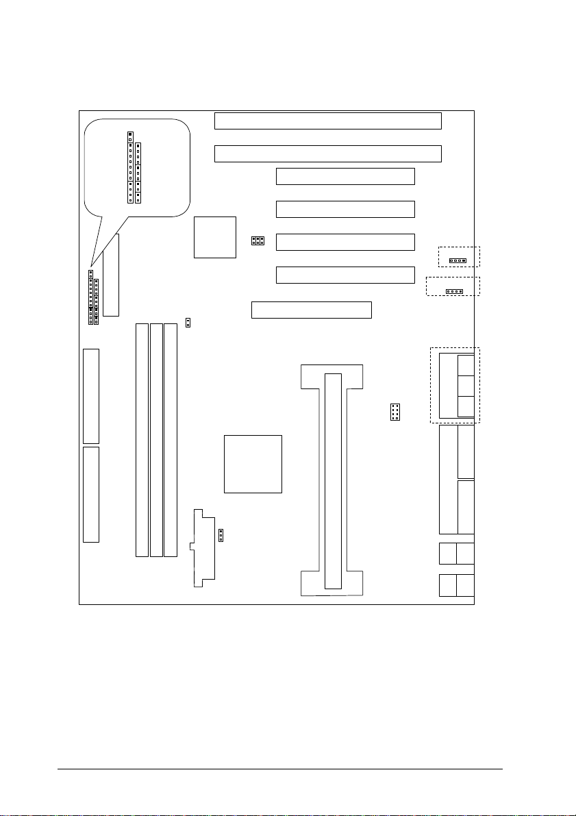
2.2 Mainboard Layout
FLOPPY Drive
DIMM 2 Socket
Primary IDE
Secondary IDE
CPU Socket
GAME Port
MOUSE
Power conn
DIMM 0 Socket
DIMM 1 Socket
LINE-
MIC
LINE-
OUT
Parallel Port
COM2
COM1
USB2
USB1
KBD
FAN (J15)
CD-IN (J27)
SLEEP(J21)
Optional
JP5
JP6Clear CMOS
HDLED
(J19)
IR(J20)
BUZZER
(J24)
PWRLED
(J18)
PWR (J22)
RESET (J23)
PIIX4
FW82371AB
16-bit ISA Slot
16-bit ISA Slot
JP7
32- bit PCI Slot
32-bit PCI Slot
32-bit PCI Slot
FW82443LX
PAC
32-bit PCI Slot
32-bit AGP Slot
MODEM J(28)
Optional
IN
Optional
2-3


3 Installation Preview
Before you install the KR630 mainboard into the system chassis you may find it convenient to
first configure the mainboard hardware. This section describes how to configure the jumper
settings, install memory modules, and how to attach the various system components. Before
using your computer you must review the following 7 steps:
1. Jumper settings
2. Installation of DRAM modules (DIMM)
3. Installation of the Slot1 Retention Module, Installation of the CPU SEC (Single Edge
Contact) Cartridge
4. Installation of expansion cards
5. Installation of IDE, I/O cables connection., and Power connection
6. Installation of the Power Core to the System.
7. Setup of the system BIOS software
3.1 Jumper Settings
You can configure the hardware options by setting jumpers on the mainboard. A jumper is a
set of two or more metal pins in a plastic base attached to the mainboard. A plastic “jumper
cap” with a metal (conductive) plate inside fits over two pins to create an electrical contact or
short between them. This contact establishes a hardware setting and is referred to as a
“closed” jumper setting.
Some jumpers have two pins while others may have three or more. Jumpers are sometimes
combined to sets called jumper blocks where all the jumpers in the block must be set
together to establish a hardware setting. In this manual, the jumper settings will be described
graphically using a triangle (s) always marking pin 1. Those jumpers with two pins will be
shown as closed or open. A jumper is closed by placing the plastic jumper cap over the two
jumper pins and is opened by removing the jumper cap. Some jumpers are oriented vertically
and others horizontally with pin 1 marked as (s=P1)
3.1.1 Jumpers, Jumper caps, and Jumper blocks
Jumper cap 2-pin jumper 3-pin jumper Jumper block
3-1
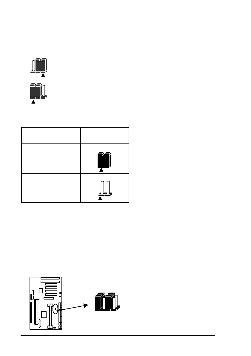
3.1.2 Setting 2-pin jumpers
1 3 5 7
Jumper Pins 1 & 2 are closed with a jumper cap
Jumper Pins 2 & 3 are closed with a jumper cap
3.1.3 CPU External (BUS) Frequency Selection (JP8)
CPU External (BUS)
Frequency Selection
60MHz
66MHz
(Manufacturer default)
JP8
3.1.4 Processor Speed setting(JP4)
The processor speed depends upon the frequency of the CLOCK GENERATOR which is
determined by jumpers. These jumpers tell the system what speed to run at. Currently, this
mainboard speed range is from 233MHz to 366MHZ. The CPU input frequency must match
the frequency of CLOCK GEN or it will cause the system to malfunction.
The Jumper located As below:
3-2
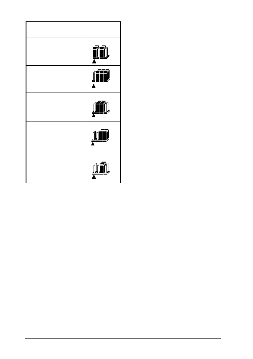
Pentium II CPU Setting
233MHz
(66MHz x3.5)
266MHz
(66MHz x 4)
(Manufacturer default)
300MHz
(66MHz x 4.5)
333MHz
(66MHz x 5)
366MHz
(66MHz x 5.5)
JP4
3.1.5 Clear CMOS(JP6)
The KR630 has a Jumper JP6, which allows you to clear the CMOS memory and Real Time
Clock (RTC) data, the CMOS memory maintains the system configuration information and
RTC provides the system with the date and time. Make sure this jumper is open for normal
operation.
Clear CMOS procedure:1.) Set JP6 to Close;2.) Power On your system; 3.) The COMOS
RAM data will be clear after POST; 4.) Power Off you system; 5.) Remove the Jumper cap;
6.) Resetting your.
3.1.6 JP5, JP7 Reserved
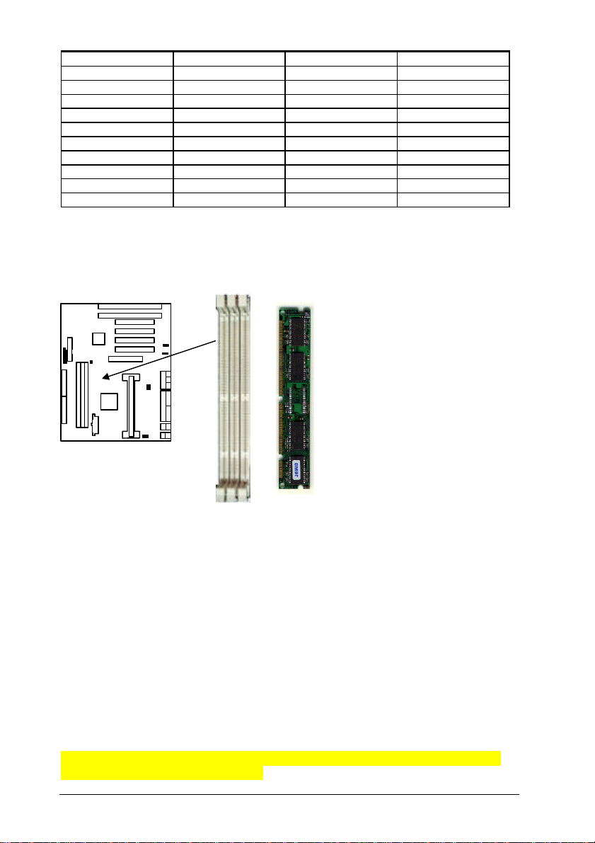
3.2 Installation of DRAM modules (DIMM)
3.2.1 DIMM (Dual Inline Memory Module)
The KR630 mainboard features three 168-pin DIMM sockets with each supporting 8MB to
64MB of SDRAM/EDO using 1MBx64, 2MBx64 and 8MBx64 DIMM
3-3

(Asymmetrical single and double sided). The DRAM interfaces on a 64-bit wide, data path.
Also supported is 3.3 volts 66.67MHz unbuffered Synchronous DRAM(SDRAM) and 3.3V
volts 60ns or faster unbuffered EDO DRAM. The EDO DRAM and SDRAM are defined
below.
3.2.2 DIMM Combinations
DIMM0 DIMM1 DIMM2 Total Memory
8MB EMPTY EMPTY 8MB
8MB 8MB EMPTY 16MB
8MB 8MB 8MB 24MB
16MB EMPTY EMPTY 16MB
16MB 8MB EMPTY 24MB
16MB 8MB 8MB 32MB
16MB 16MB EMPTY 32MB
16MB 16MB 8MB 40MB
16MB 16MB 16MB 48MB
32MB EMPTY EMPTY 32MB
32MB 8MB EMPTY 40MB
32MB 8MB 8MB 48MB
32MB 16MB EMPTY 48MB
32MB 16MB 8MB 56MB
32MB 16MB 16MB 64MB
32MB 32MB EMPTY 64MB
32MB 32MB 8MB 72MB
32MB 32MB 16MB 80MB
32MB 32MB 32MB 96MB
64MB EMPTY EMPTY 64MB
64MB 8MB EMPTY 72MB
64MB 8MB 8MB 80MB
64MB 16MB 8MB 88MB
64MB 16MB 16MB 96MB
64MB 32MB 8MB 104MB
64MB 32MB 16MB 112MB
64MB 32MB 32MB 128MB
64MB 64MB EMPTY 128MB
64MB 64MB 8MB 136MB
64MB 64MB 16MB 144MB
64MB 64MB 32MB 160MB
64MB 64MB 64MB 172MB
128MB EMPTY EMPTY 128MB
128MB 8MB EMPTY 136MB
128MB 8MB 8MB 144MB
128MB 16MB 8MB 152MB
128MB 16MB 16MB 160MB
128MB 32MB 8MB 168MB
128MB 32MB 16MB 176MB
128MB 64MB EMPTY 192MB
3-4
DIMM0 DIMM1 DIMM2 Total Memory
128MB 64MB 8MB 200MB
128MB 64MB 16MB 208MB
128MB 64MB 32MB 224MB
128MB 64MB 64MB 256MB
128MB 128MB EMPTY 256MB
128MB 128MB 8MB 264MB
128MB 128MB 16MB 272MB
128MB 128MB 32MB 288MB
128MB 128MB 64MB 320MB
128MB 128MB 128MB 384MB
3.2.3 Installation Procedure for DIMM
Insert DIMM into the DIMM
sockets at a 90 degree angle
.
1) Pin 1 of the DIMM must match with pin 1 of the DIMM socket.
2) The module will only insert into the socket one way. An orientation cut-out will
prevent you from inserting it the wrong way.
3) Insert the DIMM into the DIMM socket at a 90 degree angle. If pin 1 of the DIMM does
not line up with pin 1 of the socket, the DIMM will not insert into the socket. After
inserting the DIMM module completely into the socket, push the DIMM module into a
vertical position.
4) The module should click into place with the retaining clips at each end of the socket
snapping behind the module to secure it
5) To release the memory module push both retaining clips outwards and carefully rock the
module forward.
IMPORTANT: Do not use DIMM that use an extra TTL chip to convert the memory
module from asymmetric to symmetric.
3-5

3.3 Installation of the CPU
Socket side
The KR630 comes with Slot1 connector installing the Pentium II CPU cartridge. Before you
plug in the Pentium II CPU Cartridge, please mount the CPU Cartridge Retention module
(Packed with your mainboard) first as following step.
1. Place the Retention module over the Slot 1 connector, the Lock Holes should toward to
the DIMM socket side as following picture.
2. Tighten the 4 Captive Nuts in using a Philips or flat screw drive
The Retention Module Lock Hole
Captive Nuts
To install a CPU, flip the Pentium II CPU Cartridge locks outwards tenderly so that the lock
shows through the retention module’s side Lock Hole, and do remember to plug the CPU
FAN cable to J15.
should be towarded to DIMM
Please reference Intel Pentium II BOXed CPU Installation guide to install CPU Heat Sink
Mechanism.
WARNING: Without a fan, the Pentium II CPU Cartridge can overheat and will cause
damage to both the CPU and the KR630 mainboard. The insufficient air flow will also
damage to both the CPU and the KR630 mainboard.
3-6

3.4 Installation of Expansion Slots
3.4.1 ISA, PCI and AGP Slots
There are two types of ISA expansion cards design-Legacy and PnP (Plug & Play). For
Legacy cards you must set the cards’ jumpers manually. For Plug & Play cards, your system
will assign the IRQs and DMAs automatically. You can verify the IRQ allocation either by
using Microsoft’s Diagnostic (MSD.EXE) utility which is in the DOS directory or through the
Windows 95 resources menu.
16-bit ISA Slot
32-bit ISA Slot
3.4.2 Installation Procedure
The KR630 has 7 expansion slots on-board. There are two 16-bit ISA Bus and four 32-bit
PCI expansion slots. One of the expansion slots is shared by the connectors and will
accommodate either an ISA or a PCI expansion card, but not both at the same time. All four
PCI expansion slots accept PCI Bus master cards and fully supported by PCI 2.1
Specifications. One 32-bit AGP expansion slot. The Accelerated Graphics Port (AGP or
A.G.P.) is a high performance, component level interconnect targeted at 3D graphical display
applications and is based on a set of performance extensions or enhancements to PCI. A.G.P.
interface specification Rev. 1.0 compliant.
To install expansion cards, please read the expansion card’s documentation, which shipped
with the expansion card, for instructions.
NOTICE: Some expansion cards require an IRQ to work and may cause a conflict. There
are total of 16 IRQs but some free for expansion cards. In case of a conflict please contact the
system manufacturer for technical support.
3-7

3.5 Installation of IDE, I/O cables connection
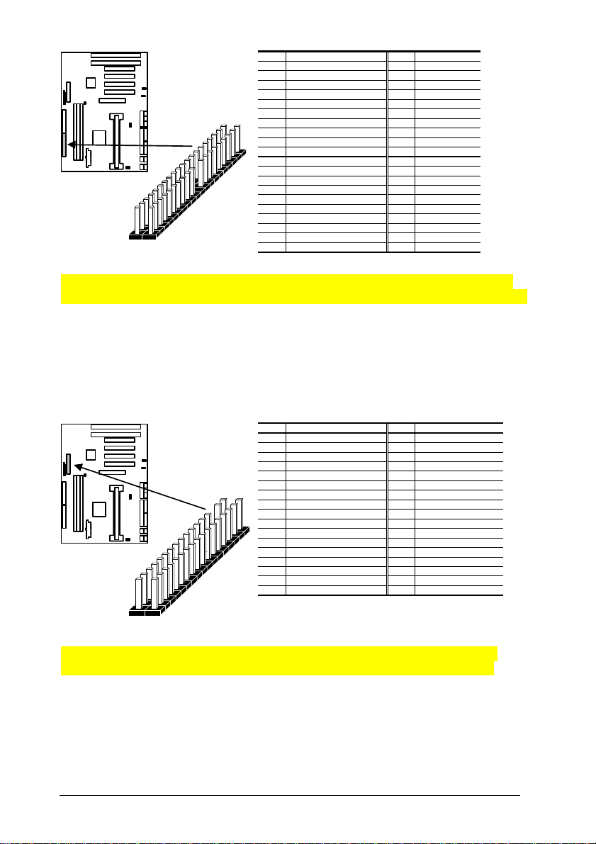
3.5.1 Primary IDE Connector (39-pin block) (J25)
This connector supports two primary channel IDE devices via a ribbon cable. When two
IDE devices are installed using the primary IDE connector make sure that the second IDE
device is set to slave mode as indicated the device’s manual.
Pin Signal Name Pin Signal Name
1 Reset IDE 2 Ground
3 Host Data 7 4 Host Data 8
5 Host Data 6 6 Host Data 9
7 Host Data 5 8 Host Data 10
9 Host Data 4 10 Host Data 11
11 Host Data 3 12 Host Data 12
13 Host Data 2 14 Host Data 13
15 Host Data 1 16 Host Data 14
17 Host Data 0 18 Host Data 15
19 Ground 20 Key
21 DDRQ0 (DDRQ1) 22 Ground
23 I/O Write # 24 Ground
25 I/O Read # 26 Ground
27 IOCHRD 28 Pull-down
29 DDACK0 (DDACK1) # 30 Ground
31 IRQ14 (IRQ15) 32 IOCS16#
33 Addr 1 34 Reserved
35 Addr 0 36 Addr 2
37 Chip Select 1P (1S) # 38 Chip Select 3P (3S)
39 Activity # 40 Ground
WARNING: When you connect a ribbon cable to these ports, you must orient the cable
connector so that the PIN 1 edge of the cable is at the PIN 1 end of the on-board connector.
3.5.2 Secondary IDE Connector (39-pin block) (J26)
This connector supports two secondary channel IDE devices and 120MB Floppy drives via a
ribbon cable. When two IDE devices are installed using the secondary IDE connector make
sure that the second IDE device is adjusted to slave mode as instructed in the device’s
manual.
3-8
Pin Signal Name Pin Signal Name
Chip Select 3P (3S)
1 Reset IDE 2 Ground
3 Host Data 7 4 Host Data 8
5 Host Data 6 6 Host Data 9
7 Host Data 5 8 Host Data 10
9 Host Data 4 10 Host Data 11
11 Host Data 3 12 Host Data 12
13 Host Data 2 14 Host Data 13
15 Host Data 1 16 Host Data 14
17 Host Data 0 18 Host Data 15
19 Ground 20 Key
21 DDRQ0 (DDRQ1) 22 Ground
23 I/O Write # 24 Ground
25 I/O Read # 26 Ground
27 IOCHRD 28 Pull-down
29 DDACK0 (DDACK1) # 30 Ground
31 IRQ14 (IRQ15) 32 IOCS16#
33 Addr 1 34 Reserved
35 Addr 0 36 Addr 2
37 Chip Select 1P (1S) # 38
39 Activity # 40 Ground
WARMING: When you connect a ribbon cable to these ports, you must orient the cable
connector so that the PIN 1 edge of the cable is at the PIN 1 end of the on-board connector.
3.5.3 Floppy Drive connector (33-pin block) (J17)
The FDC sub-system can control three types (1.2, 1.44, and 2.88MB) of floppy drivers or
compatible tape drives. Connection to floppy drives is via a header (J20). The floppy disk
interface includes 48mA drivers and Schmit inputs on the drive interface.
Pin Signal Name Pin Signal Name
1 Ground 2 DRVDEN0
3 Ground 4 Reserved
5 Key 6 DRVDEN1
7 Ground 8 FDINDX#
9 Ground 10 FDM00#
11 Ground 12 FDDS1#
13 Ground 14 FDDS0#
15 Ground 16 FDM01#
17 MSEN1 18 FDDIR#
19 Ground 20 FDSTEP#
21 Ground 22 FDWD#
23 Ground 24 FDWE#
25 Ground 26 FDTRK0#
27 Ground 28 FDWPD#
29 MID0 30 FDRDATA#
31 Ground 32 FDHEAD#
33 MIDI 34 DSKCHG#
WARNING: When you connect a ribbon cable to this port, you must orient the cable
connector so that the PIN 1 edge of the cable is at the PIN 1 end of the on-board port
3-9

3.5.4 Power Input Connector (20-pin block) (J16)
This connector supports a standard ATX power supply. When connecting, make sure the lock
key matches the hook attached on a power supply cable. The power cord should be unplugged
when you connect it.
Pin Name (Function) Pin Name (Function)
11 3.3V (Power +3.3 Voltage) 1 3.3V (Power +3.3 Voltage)
12 -12V (Power -12 Voltage) 2 3.3V (Power +3.3 Voltage)
13 Ground (Power Ground) 3 Ground (Power Ground)
14 PS_ON (Soft-Off Control) 4 +5V (Power +5 Voltage)
15 Ground (Power Ground) 5 Ground (Power Ground)
16 Ground (Power Ground) 6 +5V (Power +5 Voltage)
17 Ground (Power Ground) 7 Ground (Power Ground)
18 -5V (Power -5 Voltage) 8 PWRGD (Power Good)
19 +5V (Power +5 Voltage) 9 5VSB (Standby 5V)
20 +5V (Power +5 Voltage) 10 +12V (Power +12 Voltage)
WARNING: Make sure that the ATX Power Supply can take at least 10 mAMP load on the
5 Volt Standby lead (5VSB). You may experience difficulty in powering on your system
without this.
3.5.5 HDD LED Connector (4-pin) (J19)
The KR630 supports one straight 4 pin header for connecting to front panel Hard Disk
activity LED indicator.
Pin Signal Name
1 LED+
2 LED3 LED4 LED+
3.5.6 Reset Switch Connector (2-pin) (J23)
This connector supports the front panel case-mounted reset. It is advised that the reset witch
be used for rebooting the system in order to extend the life of the system’s power supply.
3-10

Pin Signal Name
1 Reset
2 Ground
3.5.7 Speaker Connector or on Board Buzzer(4-pin) (J24)
A1 x 4 straight header is available on the mainboard to drive a chassis-mounted speaker if
desired . The header can select between the internal Buzzer by installing a jumper between pin
3 and 4 . When the chassis mounted speaker is needed the jumper should be removed.
Pin Signal Name
1 SPKRDAT
2 No connect
3 Buzzer/Speaker Sel
4 Logic ground
3.5.8 IrDA connector (7-pin) (J20)
The KR630 mainboard offers an IrDA function. The case must reserve space for the IR
module if you want to use the IrDA function. This connector supports optional wireless
transmission and reception of infrared data. The module mounts in a small opening on the
system case that supports this feature. The efficient distance is 100cm and the transfer rate is
1.44M KB/sec.
Pin Signal Name
1 VCC
2 Key
3 IR-RX(Receive)
4 LOGIC GROUND
5 IR-TX (Transmit)
6 RX for IR Remote
7 Fast IR
3-11

IMPORTANT: You must configure this feature through the BIOS. This IR module is
supported by the mainboard via a 7-pin connector and ribbon cable.
3.5.9 CPU Fan connector (J15)
This connector supports Pentium II CPU cartridge fan power
Pin Signal Name
1 LOGIC-GROUND
2 FAN-PWR-ON
3 FANTACHI
3.5.10 Power Button Connector (J22)
This connector supports the ATX case-mounted Power Switch, which supports System
Suspend function. When the BIOS setting set the Delay 4 second to "On", the System can be
set to Suspended Mode once you push the Power Switch no longer then 4 second, otherwise
(push the Power Switch over 4 seconds) the System can be totally Power Off. When the BIOS
setting set the Delay 4 second to "Off", then Power Switch function work as regular Power
Switch.
3-12
Pin Signal Name
1 LOGIC-GROUND
2 PWRBTN

3.5.11 PS/2 Keyboard and Mouse Connector (J4)
The KR630 mainboard offers 1 PS/2 Keyboard and 1 PS/2 Mouse port as below.
PS/2 Mouse
Pin Signal Name
1 DATA
2 No connect
3 Ground
4 +5V (Fused)
5 Clock
6 No connect
PS/2 Keyboard
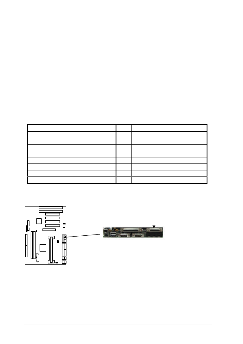
3.5.12 Universal Serial Bus (USB) Port (J8)
This KR630 mainboard has two USB on-board header. USB devices provide a more
convenient operating environment and improve data transferring capacity. True Plug-andplay, this new bus technology will support over 127 different peripherals through a Hub.
USB PORT
Pin Signal Name
1 VCC
2 -Data
3 +Data
4 Ground
3.5.13 Parallel Port Connector (25-pin Block) (J9)
The motherboard includes a bi-directional parallel port (EPP/ECP compatible). The parallel
port is capable of being disabled or remapped to either the secondary LPT address or the
primary LPT address through BIOS if other parallel ports are installed. The parallel port
contains 12mA source output drivers on the drive interface and incorporates Chip Protect
circuitry for protection against damage due to printer’s power being on.
3-13

Parallel Port
Serial Port
Serial Port
3.5.14 Serial Port (J6/J7)
The KR630 has two serial ports. The electrical characteristics are compliant with the EIA232-D Serial Communications Specifications. The serial ports may be remapped above other
installable serial ports or disabled through the BIOS.
3.5.15 Sleep button (Suspend) (J21) (Option)
The system can be forced to Suspended mode once the switch be pressed, and the BIOS
Power management setting should be Enabled.
3-14
(COM1)
(J7)
(COM2)
(J6)
Pin Signal Name
1 Ext SMI#
2 Ground
3.6 Installation of Audio connector(The Following
Sections are Available with Optional Audio Only)
The Audio Connectors on the KR630 provides access to the Line-Out, Line-In and
Microphone-In..
3.6.1 MIDI/GAME Port (J5) (Option)
For the music enthusiast the MIDI connector also provides access to receive and send MIDI
data between instruments or other MIDI capable systems. The MIDI interface is MPU-401
UART compatible with FIFOs. The same MIDI connector provides the Joystick game
compatible interface.
MIDI/GAME port Connector Pinout
PIN DESCRIPTION PIN DESCRIPTION
1 FUSED-VCC 2 F0/GAME PORT DATA 4
3 JOY3/GAME PORT DATA 0 4 LOGIC-GROUND
5 LOGIC-GROUND 6 JOY2/GAME PORT DATA 1
7 F1/GAME PORT DATA 5 8 FUSED-VCC
9 FUSED-VCC 10 F2/GAME PORT DATA 6
11 JOY1/GAME PORT DATA 2 12 TXD/MIDI TRANSMIT DATA
13 JOY0/GAME PORT DATA 3 14 F3/GAME PORT DATA 7
15 RXD/MIDI RECEIVE DATA 16 N/C
MIDI/GAME Port
3.6.2 Line Out Connector(J3)(Option)
The audio subsystem provides external sound through a user accessible stereo jack connector
(J3) soldered to the mainboard. This jack will allow the connection of self-amplified speakers.
SRS 3D sound is only available through this port.
3-15

3.6.3 Line In Connector(J1)(Option)
Line Out
Line In
An externally accessible stereo jack connector (J1) is soldered to the mainboard to allow the
connection of a stereo audio input source into the sound subsystem.
3.6.4 Microphone In Connector(J2)(Option)
An external accessible jack connector (J2) is soldered to the mainboard to allow the
connection of a microphone for voice input.
Microphone
3-16

3.6.5 Wavetable Music Synthesizer(U1 Socket Upgrade
Option)
The KR630 includes an upgrade socket for adding the Crystal CS9236 Single-Chip Wavetable
Music Synthesizer. The CS9236 is a complete General MIDI Wavetable music synthesizer on
a single integrated circuit. The MIDI interpreter, synthesis engine, effects processing and all
RAM and ROM memories (including the Wavetable sample ROM) are included on the chip.
This all-digital device receives a standard serial MIDI data stream and outputs a stereo 16-bit
digital audio stream at 44.1 kHz.
The CS9236 features a high quality General MIDI sample set including 128 melodic
instruments and 47 percussion sounds. The synthesis engine is capable of generating up to 32
simultaneous notes. Digital reverberation and chorusing effects are included on the chip.
The CS9236 is the ideal low-cost General MIDI synthesizer solution for a number of
applications, including multimedia, games, karaoke and low-cost musical instruments and
MIDI sound modules.
3.6.6 CD-IN Connector (J27)(Option)
Access to the CD-IN connector for audio input from CD-ROM drives is through a male
socket (J27) on the mainboard.
CD-IN Conn. Pinout
CD-IN Connector
PIN SIGNAL
1 GROUND
2 LEFT CHANNEL
3 GROUND
4 RIGHT CHANNEL
3.6.7 MODEM-IN Connector(J28)(Option)
Access to the MODEM-IN connector for audio input and output from the phone connection is
through a male socket on the mainboard.
3-17

MODEM-IN Conn. Pinout
PIN SIGNAL
MODEM-IN
Connector
1 GROUND
2 VOICE IN
3 GROUND
4 VOICE OUT
3-18

4 BIOS Setup
The KR630 mainboard uses an Award BIOS, which is stored in a Flash EEPROM and which
can be upgraded using a floppy disk-based program. The BIOS has a built-in Setup program
that allows users to modify the basic system configuration setting. The settings are then
stored in a dedicated batter-backed memory, called CMOS RAM, that retains the information
when the power is turned off. The BIOS provides critical low-level support for the system
central processing, memory, and I/O subsystems. The Award BIOS has been customized by
adding important, but nonstandard, features such as virus and password protection, power
management, and detailed fine-tuning of the chipset controlling the system. The rest of this
manual is intended to guide you through the process of configuring your system using Setup.
4.1 Starting Setup
The Award BIOS is immediately activated when you first turn on the computer. The BIOS
reads system configuration information in CMOS RAM and begins the process of checking
out the system and configuring it through the power-on self test (POST). When these
preliminaries are finished, the BIOS seeks an operating system on the of the data storage
devices (hard drive, floppy drive, etc.). The BIOS launches the operating system and hands
control of system operations to it.
To start Setup, press the <Del> key some time before or while a message similar to this
appears briefly at the bottom of the screen during POST:
Press DEL to enter SETUP
If the message disappears before you respond and you still wish to enter Setup, reboot the
system to try again by turning the system OFF then ON or pressing the “RESET” button on
the
system case. You may also restart by simultaneously pressing <Ctrl>, <Alt>, and <Delete>
keys. If you do not press the keys at the correct time and the system does not reboot, an error
message will be displayed at the bottom of the screen and you will again be asked to,
Press F1 to continue, DEL to enter SETUP
4.1.1 Setup Keys
These keys help you navigate in Setup:
<↑> , <↓>
<←> , <→>
<Esc>
<PgUp> / <+>
<PgDn> / <−>
Move to previous or next item
Move to the item in the left or right hand
Main Menu – Quit and not save changes into CMOS
Other Pages -- Exit current page and return to Main Menu
Increase the numeric value or make changes
Decrease the numeric value or make changes
4-1

<F1>
<F2>
<F3>
<F5>
<F7>
<F10>
General help, only for Status Page Setup Menu and Option Page
Setup Menu
Change color from total 16 colors. F2 to select Shift-F2 color
forward, Shift-F2 to select color backward
Calendar, only for Status Page Setup Menu
Restore the previous CMOS value from CMOS, only for Option
Page Setup Menu
Load the Setup default
Save all the CMOS changes, only for Main Menu
4.1.2 Getting Help
Press F1 to pop up a small help window that describes the appropriate keys to use and the
possible selections for the highlighted item. To exit the Help Window press Esc or the F1 key
again.
4.1.3 In Case of Problems
If after making and saving system changes with Setup, you discover that your computer no
longer is able to boot, the Award BIOS supports an override to the CMOS settings that resets
your system to its default configuration.
You can invoke this override by immediately pressing Insert; when you restart your computer
You can restart by either using the ON/OFF switch, the RESET button or by pressing CtrlAlt-Delete.
The best advice is to alter only settings that you thoroughly understand. In particular, do not
change settings in the Chipset screen without a good reason. The Chipset defaults have been
carefully chosen by Award or your system manufacturer for the best performance and
reliability. Even a seemingly small change to the Chipset setup may causing the system to
become unstable.
4-2

4.2 Main Setup Menu
When you enter the Award BIOS CMOS Setup Utility, a Main Menu (Figure 1) appears on
the screen. The Main Menu allows you to select from several Setup functions and two exit
choices. Use the arrow keys to select among the items and press Enter to accept and enter the
sub-menu.
A brief description of each highlighted selection appears at the bottom of the screen.
ROM PCI/ISA BIOS (2A69JB3A)
CMOS SETUP UTILITY
STANDARD CMOS SETUP INTEGRATED PERIPHERALS
BIOS FEATURE SETUP SUPERVISOR PASSWARD
CHIPSET FEATURES SETUP USER PASSWARD
POWER MANAGEMENT SETUP IDE HDD AUTO DETECTION
PNP/PCI CONFIGURATION SAVE & EXIT SETUP
LOAD SETUP DEFAULTS EXIT WITHOUT SAVING
ESC : Quit
F10 : Save & Exit Setup (Shift)F2 : Change Color
Following is a brief summary of each Setup category.
Standard CMOS Options in the original PC AT-compatible BIOS.
BIOS Features Award enhanced BIOS options.
Chipset Features Options specific to your system chipset.
Power
Advanced Power Management (APM) options.
Management
PnP/PCI
Configuration
Integrated
Peripherals
Supervisor/User
Password Setting
Plug and Play standard and PCI Local Bus configuration
options.
I/O subsystems that depend on the integrated peripherals
controller in your system.
Change, set, or disable a password. In BIOS versions that
allow separate user and supervisor passwords, only the
supervisor password permits access to Setup. The user
password generally allows only power-on access.
IDE HDD Auto
Automatically detect and configure IDE hard disk parameters.
Detection
Load Setup
Defaults
Setup defaults are factory settings for optimal-performance
system operations.
Save & Exit Setup Save settings in nonvolatile CMOS RAM and exit Setup.
Exit Without Save Abandon all changes and exit Setup.
AWARD SOFTWARE, INC.
↑↑ ↓↓ →→ ←← : Select Item
Time, Date Hard Disk Type…
Figure 1
4-3

4.3 Standard CMOS Setup Menu
In the Standard CMOS Menu (Figure 2) you can set the system clock and calendar, record
disk drive parameters and the video subsystem type, and select the type of errors that stop the
BIOS POST.
ROM PCI/ISA BIOS (2A69JB3A)
STANDARD CMOS SETUP
AWARD SOFTWARE, INC.
Date (mm:dd:yy) : Sun,
Time (hh:mm:ss) :
HARD DISKS TYPE SIZE CYLS HEAD PRECOMP
Primary Master :
Primary Slave :
Secondary Master :
Secondary Slave :
Drive A :
Drive B :
Video :
Halt On :
ESC : Quit
F1 : Help (Shift)F2 : Change Color
May 12 19996
10 : 10 : 00
1.44MB, 3.5 in.
None
EGA/VGA
All Errors
↑ ↓ → ←
Auto
Auto
Auto
Auto
: Select Item PU/PD/+/- : Modify
0 0 0 0
0 0 0 0
0 0 0 0
0 0 0 0
Base Memory: 640K
Extended Memory: 31744K
Other Memory: 384K
Total Memory: 32768K
Figure 2
4.3.1 Date
The BIOS determines the day of the week from the other date information. This field is for
information only. Press the left or right arrow key to move to the desired field (date, month,
year). Press the PgUp or PgDn key to increment the setting, or type the desired value into the
field.
4.3.2 Time
The time format is based on the 24-hour military-time clock. For example, 1 p.m. is 13:00:00.
Press the left or right arrow key to move to the desired field. Press the PgUp or PgDn key to
increment the setting, or type the desired value into the field.
4.3.3 Hard Disks
The BIOS supports up to four IDE drives. This section does not show information about ther
IDE devices, such as a CD-ROM drive, or about other hard drive types, such as SCSI drives.
NOTE: We recommend that you select type AUTO for all drives.
The BIOS can automatically detect the specifications and optimal operating mode of almost ll
IDE hard drives. When you select type AUTO for a hard drive, the BIOS detects its
specifications during POST, every time the system boots.
4-4

If you do not want to select drive type AUTO, other methods of selecting the drive type are
available:
1) Match the specifications of your installed IDE hard drive(s) with the preprogrammed
values for drive types 1 through 45.
2) Select USER and enter values into each drive parameter field.
3) Use the IDE HDD AUTO DECTECTION function in Setup.
Here is a brief explanation of drive specifications:
• Type: The BIOS contains a table of pre-defined drive types. Each defined drive type has
a specified number of cylinders, number of heads, write precompensation factor,
landing zone, and number of sectors, Drives whose specifications do not accommodate
any pre-defined type are classified as type USER.
• Size: Disk drive capacity (approximate). Note that this size is usually slightly greater
than the size of a formatted disk given by a disk-checking program.
• Cyls: Number of cylinders
• Head: Number of herds
• Precomp: Write precompensation cylinder
• Landz: Landing zone
• Sector: Number of sectors
• Mode: Auto, Normal, large, or LBA
• Auto: The BIOS automatically determines the optimal mode.
• Normal: Maximum number of cylinders, heads, and sectors supported are 1024, 16,
and 63.
• Large: For drives that do not support LBA and have more than 1024 cylinders.
• LBA (Logical Block Addressing): During drive accesses, the IDE controller
transforms the data address described by sector, head, and cylinder number into a
physical block address, significantly improving data transfer rates. For drives with
greater than 1024 cylinders.
4-5

4.3.4 Drive A/B type
Select the correct specifications for the diskette drive(s) installed in the computer.
None No diskette drive installed
360K, 5.25 in 5-1/4 inch PC-type standard drive; 360 kilobyte capacity
1.2M, 5.25 in 5-1/4 inch AT-type high-density drive; 1.2 megabyte capacity
720K, 3.5 in 3-1/2 inch double-sided drive; 720 kilobyte capacity
1.44M, 3.5 in 3-1/2 inch double-sided drive; 1.44 megabyte capacity
2.88M, 3.5 in 3-1/2 inch double-sided drive; 2.88 megabyte capacity
4.3.5 Video
Select the type of primary video subsystem in your computer. The BIOS usually detects the
correct video type automatically. The BIOS supports a secondary video subsystem, but you
do not select it in Setup.
EGA/VGA
CGA 40 Color Graphics Adapter, power up in 40 column mode.
CGA 80 Color Graphics Adapter, power up in 80 column mode.
MONO Monochrome adapter, includes high resolution monochrome adapters.
Enhanced Graphics Adapter/Video Graphics Array. For EGA, VGA,
SEGA, SVGA or PGA monitor adapters.
4.3.6 Halt on
During the power-on self-test (POST), the computer stops if the BIOS detects a hardware
error. You can tell the BIOS to ignore certain errors during POST and continue the boot-up
process. These are the selections:
No errors POST does not stop for any errors.
All errors If the BIOS detects any non-fatal error, POST stops and prompts
you to take corrective action.
All, But
Keyboard
All, But Diskette POST does not stop for diskette drive errors, but stops for all
All, But Disk/Key POST does not stop for a keyboard or disk error, but stops for all
POST does not stop for a keyboard error, but stops for all other
errors.
other errors.
other errors.
4.3.7 Memory
You cannot change any values in the Memory fields; they are only for your information. The
fields show the total installed random access memory (RAM) and amounts allocated to base
memory, extended memory, and other (high) memory, RAM is counted in kilobytes (KB:
approximately one thousand bytes) and megabytes (MB: approximately one million bytes).
4-6

RAM is the computer’s working memory, where the computer stores programs and data
currently being used, so they are accessible to the CPU. Modern personal computers may
contain up to 64MB, 128MB, or more.
Base Memory
Typically 640 KB. Also called conventional memory. The DOS operating system and
conventional applications use this area.
Extended Memory
Above the 1-MB boundary. Early IBM personal computers could not use memory above 1
MB, but current PCs and their software can use extended memory.
Other Memory
Between 640 KB and 1 MB; often called High memory. DOS may load terminate-and-stayresident (TSR) programs, such as device drivers, in this area, to free as much conventional
memory as possible for applications. Lines in your CONFIG.SYS file that start with
LOADHIGH load programs into high memory
Total memory
System total memory is the sum of base memory, extended memory, and other memory.
4-7

4.4 BIOS Features Setup Menu
This screen (Figure 3)contains industry-standard options additional to the core PC AT BIOS.
This section describes all fields offered by Award Software in this screen. Some fields may
vary from those in your Setup program. Your system board designer may omit or modify
some fields.
Virus Warning :
External Cache :
Quick Power On Self Test :
Boot Sequence :
Swap Floppy Drive :
Boot Up Floppy Seek :
Boot Up Numlock Status :
Typematic Rate Setting :
Typematic Rate (Chars/Sec) :
Typematic Delay (Msec) :
Security Option :
Assign IRQ For VGA :
OS Select For DRAM > 64MB :
4.4.1 Virus Warning
When enabled, you receive a warning message if a program (specifically, a virus) attempts to
write to the boot sector or the partition table of the hard disk drive. You should then run an
anti-virus program. Keep in mind that this feature protects only the boot sector, not the entire
hard drive.
ROM PCI/ISA BIOS (2A69JB3A)
BIOS FEATURES SETUP
AWARD SOFTWARE, INC.
Disabled
Enabled
Enabled
C,A
Disabled
Enabled
On
Disabled
6
250
Setup
Disabled
Non-OS2
Video BIOS Shadow :
C8000-CBFFF Shadow :
CC000-CFFFF Shadow :
D0000-D3FFF Shadow :
D4000-D7FFF Shadow :
D8000-DBFFF Shadow :
D8000-DFFFF Shadow :
ESC : Quit
F1 : Help PU/PD/+/- : Modify
F5 : Old Values (Shift)F2 : Color
F7 : Load Setup Defaults
Figure 3
↑↓→←
Enabled
Disabled
Disabled
Disabled
Disabled
Disabled
Disabled
: Select Item
NOTE: Many disk diagnostic programs that access the boot sector table can trigger the virus
warning message. If you plan to run such a program, we recommend that you first disable the
virus warning.
4.4.2 CPU Level 1/Level 2 Cache
Cache memory is additional memory that is much faster than conventional DRAM (system
memory). Pentium II CPU has Level 1 and Level 2 build-in cache. These fields allow you to
Enabled (Default) or Disabled to turn on or turn off the memory cache ability.
4.4.3 Boot Sequence
The original IBM PCs loaded the DOS operating system from drive A (floppy disk), so IBM
PC-compatible systems are designed to search for an operating system first on drive A, and
then on drive C (hard disk). However, the BIOS now offers 10 different boot sequence
4-8

options of three drives each. In addition to the traditional drives A and C, options include
IDE hard drives D,E, and F; plus a SCSI hard drive and a CD-ROM drive.
4.4.4 Swap Floppy Drive
This field is effective only in systems with two floppy drives. Selecting Enabled assigns
physical drive B to logical drive A, and physical drive A to logical drive B.
4.4.5 Boot Up Floppy Seek
When Enabled, the BIOS tests (seeks) floppy drives to determine whether they have 40 or 80
tracks. Only 360-KB floppy drives have 40 tracks; drives with 720 KN< 1.2MB, and 1.44MB
capacity all have 80 tracks. Because very few modern PCs have 40-track floppy drives, we
recommend that you set this field to Disabled to save time.
4.4.6 Boot Up NumLock Status
Toggle between On or off to control the state of the NumLock key when the system boots.
When toggled On, the numeric keypad generates numbers instead of controlling cursor
operations.
4.4.7 Typematic Rate Setting
When Disabled, the following two items (Typematic Rate and Typematic Delay) are
irrelevant. Keystrokes repeat at a rate determined by the keyboard controller in your system.
When Enabled, you can select a typematic a\rate and typematic delay.
4.4.8 Typematic Rate (Chars/Sec)
When the typematic rate setting is enabled, you can select a typematic rate (the rate at which
character repeats when you hold down a key) of 6,8,10,12,15,20,24, or 30 characters per
second.
4.4.9 Typematic Delay (Msec)
When the typematic rate setting is enabled, you can select a typematic delay (the delay before
key strokes begin to repeat) of 250, 500, 750 or 1000 milliseconds.
4.4.10 Security Option
If you have set a password, select whether the password is required every time the System
boots, or only when you enter Setup.
4-9

4.4.11 PCI/VGA Palette Snoop
Some display cards that are not standard VGA such as graphics accelerators or MPEG cards
may not show the correct colors, the setting can correct this problem once you set it to Enable,
To default setting leave at Disabled.
4.4.12 OS select for DRAM>64MB
Select OS2 only if you are running OS/2 operating system with greater than 64MB of RAM
on your system.
4.4.13 Shadow
Software that resides in a read-only memory (ROM) chip on a device is called firmware. The
Award BIOS permits shadowing of firmware such as the system BIOS, video BIOS, and
similar operating instructions that come with some expansion peripherals, such as, for
example, a SCSI adapter.
Shadowing copies firmware from ROM into system RAM, where the CPU can read it through
the 16-bit or 32-bit DRAM bus. Firmware not shadowed must be read by the system through
the 8-bit x-bus. Shadowing improves the performance of the system BIOS and similar ROM
firmware for expansion peripherals, but it also reduces the amount of high memory (640KB to
1 MB) available for loading device drivers, etc.
Enable shadowing into each section of memory separately. Many system designers hardwire
shadowing of the system BIOS and eliminate a System BIOS Shadow option.
Video BIOS shadows into memory area C0000-C7FFF> The remaining areas shown on the
BIOS Features Setup screen may be occupied by other expansion card firmware. If an
expansion peripheral in your system contains ROM-based firmware, you need to know the
address range the ROM occupies to shadow it into the correct area of RAM.
4-10

4.5 Chipset Features Setup Menu
↑ ↓ → ←
Auto Configuration : Enabled SDRAM CAS latency Time : 3
DRAM Speed Selection : 60ns
DRAM ECC/PARITY Select : Disabled
System BIOS Cacheable : Enabled
Video BIOS Cacheable : Enabled
8 bit I/O Recovery Time : 1
16 bit I/O Recovery Time : 1
Memory Hole At 15M-16M : Disabled
Passive Release : Enabled
Delayed Transaction : Enabled
ROM PCI/ISA BIOS (2A69JB3A)
CHIPSET FEATURES SETUP
AWARD SOFTWARE, INC.
ESC : Quit
Item
F1 : Help PU/PD/+/- : Modify
F5 : Old Values (Shift)F2 : Color
F7 : Load Setup Defaults
: Select
Figure 4
4.5.1 Auto Configuration
Auto Configuration selects predetermined optimal values of chipset parameters. When
Disabled, chipset parameters revert to setup information stored in CMOS. Many fields in this
screen are not available when Auto Configuration is Enabled.
4.5.2 DRAM Speed Selection
The value in this field must correspond to the speed of the DRAM installed in your system.
DO NOT change the default setting of this fields, as determined by the system board
manufacturer for the installed DRAM. This value is access speed, so a lower value means a
faster system.
4.5.3 DRAM ECC/Parity Select
Select Parity, ECC, or Disabled, depending on the type of DRAM installed in your system.
Also you need install Pentium II CPU cartridge with ECC support for ECC function properly
once you installed 36-bit SIMM.
4.5.4 System BIOS Cacheable
Select Enabled allows caching of the system BIOS ROM at F000h-FFFFFh, resulting in
better system performance. However, if any program writes to this memory area, a system
error may result.
4.5.5 Video BIOS Cacheable
Select Enabled allows caching of the video BIOS ROM at F0000h-FFFFFh, resulting in better
system performance. However, if any program writes to this memory area, a system error
may result.
4-11

4.5.6 8 Bit I/O Recovery Time
The recovery time is the length of time, measured in CPU clocks, which the system will delay
after the completion of an input/output request. This delay takes place because the CPU is
operating so much faster than the input/output bus that the CPU must be delayed to allow for
the completion of the I/O.
This item allows you to determine the recovery time allowed for 8 bit I/O. Choices are from
NA, 1 to 8 CPU clocks.
4.5.7 16 Bit I/O Recovery Time
This item allows you to determine the recovery time allowed for 16 bit I/O. Choices are from
NA, 1 to 4 CPU clocks.
4.5.8 Memory Hole At 15M-16M
In order to improve performance, certain space in memory can be reserved for ISA cards.
This memory must be mapped into the memory space below 16 MB. You can reserve this
area of system memory for ISA adapter ROM. When that area is reserved it cannot be
cached. The user information of peripherals that need to use this area of system memory
usually discusses their memory requirements.
4.5.9 Passive Release
When Enabled, CPU to PCI bus accesses are allowed during passive release. Otherwise, the
arbiter only accepts another PCI master access to local DRAM.
4.5.10 Delayed Transaction
The chipset has an embedded 32-bit posted write buffer to support delay transactions cycles.
Select Enabled to support compliance with PCI specification version 2.1.
4-12

4.6 Power Management Setup Menu
ROM PCI/ISA BIOS (2A69JB3A)
POWER MANAGEMENT SETUP
AWARD SOFTWARE, INC.
Power Management :
PM Control by APM :
Video Off Method :
Video off After Suspend : Yes Primary IDE 1 : Disabled
Doze Mode : Disable Secondary IDE 1 : Disabled
Standby Mode : Disable Floppy Disk : Disabled
Suspend Mode : Disable Serial Port : Disabled
HDD Power Down : Disable Parallel Port : Disabled
VGA Active Monitor : Disabled
PWR-BTTN: : Delay 4 sec.
Resume by Ring : Disabled
Break Event From Suspend
IRQ8 clock event :
4.6.1 Power Management
This option allows you to select the type (or degree) of power saving for Doze, Standby, and
Suspend modes. See the section PM Timers for a brief description of each mode. This table
describes each power management mode:
Disable Global Power Management will be disabled
Max Saving Maximum power savings. Only Available for SL CPUs. Inactivity
period is 1 minute in each mode.
User Define Set each mode individually. Select time-out periods in the PM Timers
section, following.
Min Saving Minimum power savings. Inactivity period is 1 hour in each mode
(except the hard drive).
Disable
Yes
V/H SYNC+Blank
Disabled
Figure 5
** Reload Global Timer Events **
IRQ [3-7,9-15], NMI : Disabled
Primary IDE 0 : Disabled
Secondary IDE 0 : Disabled
ESC : Quit
F1 : Help PU/PD/+/- : Modify
F5 : Old Values (Shift)F2 : Color
F7 : Load Setup Defaults
↑↓→←
: Select Item
4.6.2 PM Control by APM
If Advanced Power Management (APM) is installed on your system, selecting Yes gives better
power savings.
4.6.3 Video Off Method
Determines the manner in which the monitor is blanked.
V/H
SYNC+Blank
System turns off vertical and horizontal synchronization ports and
writes blanks to the video buffer.
DPMS Support Select this option if your monitor supports the Display Power
Management Signaling (DPMS) standard of the Video Electronics
Standards Association (VESA). Use the software supplied for your
video subsystem to select video power management values.
Blank Screen System only writes blanks to the video buffer.
4-13

4.6.4 Video Off After
As the system moves from lesser to greater power-saving modes, select the mode in which
you want the monitor to blank.
4.6.5 Doze Mode
Defines the continuous idle time before the system entering DOZE mode. The range is from 1
min to 1 Hr. If any item defined is enabled & active, STANDBY timer will be reloaded
4.6.6 Standby Mode
After the selected period of system inactivity (1 minute to 1 hour), the fixed disk drive and the
video shut off while all other devices still operate at full speed.
4.6.7 Suspend Mode
After the selected period of system inactivity (1 minute to 1 hour), all devices except the CPU
shut off.
4.6.8 HDD Power Down
After the selected period of drive inactivity (1 to 15 minutes), the hard disk drive powers
down while all other devices remain active.
4.6.9 VGA Active Monitor
When Enabled, any video activity restarts the global timer for Standby mode.
4.6.10 Soft-Off by PWR-BTTN
When this feature set to “Delay 4 sec.” , the system will become suspend once the Power
Switch be pressed within 4 second, and the system will Power Off once the Power Switch be
pressed over 4 second. If it set to “Instant Off”, the system will unconditional Power Off once
the Power Switch be pressed.
4.6.11 Resume by Ring
The system will be awaked by telephone ring if this feature set to Enable
4-14

4.6.12 IRQ8 Clock Event
You can turn On or Off monitoring of IRQ8 (the Real Time Clock) so it does not awaken the
system from Suspend mode.
4.6.13 Reload global Timer Events
When Enabled, an event occurring on each device listed below restarts the global time for
Standby mode.
q IRQ3 -7, 9-15, NMI
q Primary IDE 0
q Primary IDE 1
q Secondary IDE 0
q Secondary IDE 1
q Floppy Disk
q Serial Port
q Parallel Port
4-15

4.7 PCI Configuration Setup Menu
ROM PCI/ISA BIOS (2A69JB3A)
PNP/PCI CONFIGURATION SETUP
AWARD SOFTWARE, INC.
Resources Controlled by :
PNP OS Installed :
Reset Configuration Data :
IRQ-3 assigned to :
IRQ-4 assigned to :
IRQ-5 assigned to :
IRQ-7 assigned to :
IRQ-9 assigned to :
IRQ-10 assigned to :
IRQ-11 assigned to :
IRQ-12 assigned to :
IRQ-14 assigned to :
IRQ-15 assigned to :
DMA-0 assigned to :
DMA-1 assigned to :
DMA-3 assigned to :
DMA-5 assigned to :
DMA-6 assigned to :
DMA-7 assigned to :
Manual
Off
Disabled
Legacy ISA
Legacy ISA
Legacy ISA
Legacy ISA
Legacy ISA
Legacy ISA
Legacy ISA
Legacy ISA
Legacy ISA
Legacy ISA
Legacy ISA
Legacy ISA
Legacy ISA
Legacy ISA
Legacy ISA
Legacy ISA
PCI IDE IRQ Map To :
Primary IDE INT# :
Secondary IDE INT# :
ESC : Quit
F1 : Help PU/PD/+/- : Modify
F5 : Old Values (Shift)F2 : Color
F7 : Load Setup Defaults
Figure 6
4.7.1 PNP OS Installed
The default setting is No when a non PNP OS installed or to prevent reassigning of interrupt
setting for some of non PNP cards installed. Select Yes if the OS is PNP aware (e.g.
Windows 95).
4.7.2 Resources Controlled by
The Award Plug and Play BIOS can automatically configure all the boot and Plug and Playcompatible devices. If you select Auto, all the interrupt request (IRQ) and DMA assignment
fields disappear, as the BIOS automatically assigns them.
↑↓→←
PCI-AUTO
A
B
: Select Item
4.7.3 Reset Configuration Data
Normally, you leave this field Disabled. Select Enabled to reset Extended System
Configuration Date (ESCD) when you exit Setup if you have installed a new add-on and the
system reconfiguration has caused such a serious conflict that the operating system cannot
boot.
4.7.4 IRQ # Assigned to
When resources are controlled manually, assign each system interrupt as one of the following
types, depending on the type of device using the interrupt.
4-16

Legacy ISA Devices compliant with the original PC AT bus specification, requiring a specific
interrupt (such as IRQ4 for serial port 1).
PCI/ISA PnP Devices compliant with the Plug and Play standard, whether designed for PCI or
ISA bus architecture.
4.7.5 DMA # Assigned to
When resources are controlled manually, assign each system DMA channel as one of the
following types, depending on the type of device using the interrupt:
Legacy ISA Devices compliant with the original PC AT bus specification, requiring a specific
DMA channel.
PCI/ISA PnP Devices compliant with the Plug and Play standard, whether designed for PCI or
ISA bus architecture.
4.7.6 PCI IRQ Activated by
Leave the IRQ trigger set at Level unless the PCI device assigned to the interrupt specifies
Edge-triggered interrupts.
4.7.7 PCI IDE IRQ Map To
This field lets you select PCI IDE IRQ mapping or PC AT (ISA) interrupts. If your system
does not have one or two PCI IDE connectors on the system board, select values according to
the type of IDE interface(s) installed in your system (PCI or ISA). Standard ISA interrupts for
IDE channels are IRQ14 for primary and IRQ15 for secondary.
4.7.8 Primary/Secondary IDE INT#
Each PCI peripheral connection is capable of activating up to four interrupts: INT$ A, INT#
B, INT# C and INT#D. By default, a PCI connection s assigned INT3 A. Assigning INT#B
has no meaning unless the peripheral device requires two interrupt services rather than just
one. Because the PCI IDE interface in the chipset has two channels, it requires two interrupt
services. The primary and secondary IDE INT# fields default to values appropriate for two
PCI IDE channels, with the primary PCI IDE channel having a lower interrupt than the
secondary.
4-17

4.8 Integrated peripherals Menu
IDE HDD Block Mode : Disabled Onboard Parallel Port : 378/IRQ7
IDE Primary Master PIO : Auto Parallel Port Mode : ECP
IDE Primary Slave PIO : Auto ECP Mode use DMA : 3
IDE Secondary Master PIO : Auto
IDE Secondary Slave PIO : AUTO
IDE Primary Master UDMA : AUTO
IDE Primary Slave UDMA : AUTO
IDE Secondary Master UDMA : Auto
IDE Secondary Slave UDMA : Auto
USB Keyboard Support : Disabled
Onboard FDD Controller : Enabled
Onboard Serial Port 1 : 3F8/IRQ4
Onboard Serial Port 2 : 2F8/IRQ3 F1 : Help PU/PD/+/- : Modify
UART2 Mode : Standard F5 : Old Values (Shift)F2 : Color
ROM PCI/ISA BIOS (2A69JB3A)
INTEGRATED PERIPHERALS SETUP
AWARD SOFTWARE, INC.
ESC : Quit ↑↓→← : Select Item
F7 : Load Setup Defaults
Figure 7
4.8.1 IDE HDD Block Mode
Block mode is also called block transfer, multiple commands, or multiple sector read/write. If
your IDE hard drive supports block mode (most new drives do), select Enabled for automatic
detection of the optimal number of block read/writes per sector the drive can support.
4.8.2 On-Chip Primary/Secondary PCI IDE
The integrated peripheral controller contains an IDE interface with support for two IDE
CHANNELS. Select Enabled to activate each channel separately.
4.8.3 Onboard FDC Controller
Select Enabled if your system has a floppy disk controller (FDC) installed on the system
board and you wish to use it. If you install an add-in FDC or the system has no floppy drive,
select disabled in this field.
4.8.4 Onboard Serial Port 1/2
Select an address and corresponding interrupt for the first and second serial ports.
4.8.5 UART2 Mode
Select the UART2 mode, there are 2 option Standard or IrDA.
4-18

4.8.6 Onboard Parallel Port
Select a logical LPT port name and matching address for the physical parallel (printer) port.
4.8.7 Onboard Parallel Mode
Select an operating mode for the onboard parallel (printer) port. Select Normal unless your
hardware and software require one of the other modes offered in this field.
SPP Standard parallel port mode (Default)
EPP Bi-directional mode
ECP Fast, buffered
ECP+EPP Bi-directional and buffered
4.8.8 ECP Mode Use DMA
Select a DMA channel for the port.
4.8.9 USB Keyboard Support
Select Enabled if your system contains a Universal Serial Bus (USB) controller and you have
a USB keyboard.
4-19

4.9 IDE HDD Auto Detection
BIOS setup will display all possible modes that supported by the HDD including NORMAL,
LBA & LARGE.
If HDD does not support LBA modes, no ‘LBA” option will be shown.
If no of cylinders is less than or equal to 1024, no “LARGE” option will be show
Users can select a mode which is appropriate for them.
4.10 Password Setting
When you select this function, a message appears at the center of the screen:
ENTER PASSWORD:
Type the password, up to eight characters, and press Enter. Typing a password clears any
previously entered password from CMOS memory. Now the message changes:
CONFIRM PASSWARD:
Again, type the password and press Enter.
To abort the process at any time, press Esc.
In the Security Option item in the BIOS Features Setup screen select System or Setup:
System Enter a password each time the system boots and whenever you enter Setup.
Setup Enter a password whenever you enter Setup.
NOTE: To clear the password, simply press Enter when asked to enter a password. Then the
password function is disabled.
4-20

Documentation Rev. Number. A01(August, 1997)
4-21
 Loading...