BCD Semiconductor AM5668 Service Manual

Data Sheet
5-CHANNEL MOTOR DRIVER FOR DVD PLAYER AM5668
General Description
The AM5668 is a five-channel BTL driver IC, in
which four channels are voltage-type BTL drivers for
tracking and focus actuators, sled and spindle motors,
the other one channel is DC motor driver for tray
which supports forward/reverse control. This IC also
contains two general-purpose independent precise
voltage comparators.
The AM5668 is available in standard HSOP-28 package.
Features
· 4-Channel DC Motor BTL Driver
· 1-Channel Forward/Reverse Control DC Motor
BTL Driver
· Two Bui lt-in Com parators
· Built-in Level Shift Circuit
· Built-in Mute Mode
· Built-in Thermal Shutdown Circuit
· Operating Voltage: 4.3V to 13.2V
Application
· DVD Player Driver
Sep. 2005 Rev. 1. 2
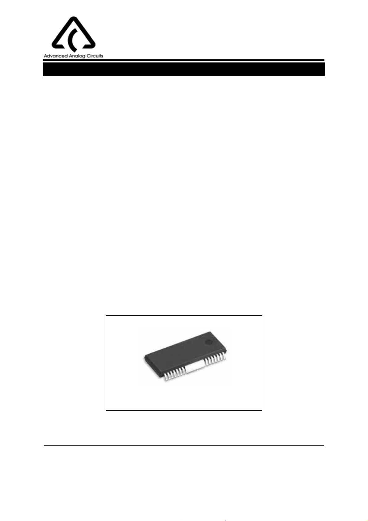
HSOP-28
Figure 1. Package Type of AM5668
BCD Semiconductor Manufacturing Limited
1

Data Sheet
5-CHANNEL MOTOR DRIVER FOR DVD PLAYER AM5668
Pin Configuration
M Package
(HSOP-28)
VINFC
OP2INOP2IN+
VINSL
OP2OUT OP1IN-
FWD
REV
(PGND)
V
CC1
VOTR-
VOTR+
1
2
3
4
5
6
7
8
9
10
28
27
26
25
24
23
22
21
20
19
MUTE
BIAS
VINTK
OP1IN+
VINSP
GND
(PGND)
VCTL
OP1OUT
V
CC2
Sep. 2005 Rev. 1. 2
VOSL+
VOSL-
VOFC-
VOFC+
11
12
13
14
Figure 2. Pin Configuration of AM5668 (Top View)
18
17
16
15
BCD Semiconductor Manufacturing Limited
2
VOSP-
VOSP+
VOTK-
VOTK+

Data Sheet
5-CHANNEL MOTOR DRIVER FOR DVD PLAYER AM5668
Pin Description (Note 1)
Pin Number Pin Name Function
1 VINFC Input for focus driver
2 OP2IN- Comparator 2 input (-)
3 OP2IN+ Comparator 2 input (+)
4 VINSL Input for the sled driver
5 OP2OUT Comparator 2 output
6 FWD Tray driver forward input
7 REV Tray driver reverse input
8V
9 VOTR- Tray driver output (-)
10 VOTR+ Tray driver output (+)
11 VOSL+ Sled driver output (+)
12 VOSL- Sled driver output (-)
13 VOFC- Focus driver output (-)
14 VOFC+ Focus driver output (+)
15 VOTK+ Tracking driver output (+)
16 VOTK- Tracking driver output (-)
17 VOSP+ Spindle driver output (+)
18 VOSP- Spindle driver output (-)
19 V
20
21 VCTL Speed control input of tray driver
22 GND Ground
23 VINSP Input for spindle driver
24 OP1IN25 OP1IN+
26 VINTK Input for tracking driver
27 BIAS Input for reference voltage
28 MUTE Input for mute control
CC1
CC2
OP1OUT
VCC for pre-driver block and power block of sled and tray
VCC for power block of spindle, tracking and focus
Comparator 1 output
Comparator 1 input (-)
Comparator 1 input (+)
Note 1: Symbols of + and - (output of drivers) mean polarity with respect to input pin.
(For example, if voltage of pin 1 is high, pin 14 is high and pin 13 is low. )
Sep. 2005 Rev. 1. 2
BCD Semiconductor Manufacturing Limited
3

Data Sheet
5-CHANNEL MOTOR DRIVER FOR DVD PLAYER AM5668
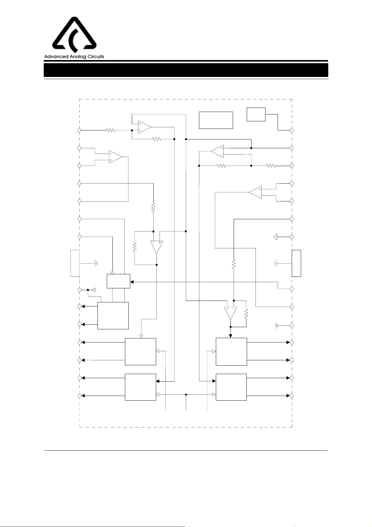
Functional Block Diagram
VINFC
OP2IN-
OP2IN+
VINSL
OP2OUT
FWD
REV
V
CC1
VOTR-
VOTR+
VOSL+
VOSL-
1
2
3
4
5
6
7
8
10
11
12
THERMAL
SHUT DOWN
17K
42.5K
MUTE
28
MUTE
27
BIAS
26
42.5k 17k
VINTK
25
OP1IN+
24
OP1IN-
17K
23
VINSP
22
GND
42.5K
PGND
V
CC1
Pre-DRV
17K
9
PGND
21
VCTL
20
OP1OUT
TRAY
DRIVER
25.5K
19
V
CC2
V
CC2
18
SLED
DRIVER
(4X)
SPINDLE
DRIVER
(4X)
17
VOSP-
VOSP+
VOFC-
13
14 15
VOFC+
Sep. 2005 Rev. 1. 2
ACTUATOR
DRIVER
(6X)
V
V
CC1
CC2
V
ACTUATOR
DRIVER
(6X)
CC2
Figure 3. Functional Block Diagram of AM5668
BCD Semiconductor Manufacturing Limited
4
16
VOTK-
VOTK+

Data Sheet
5-CHANNEL MOTOR DRIVER FOR DVD PLAYER AM5668
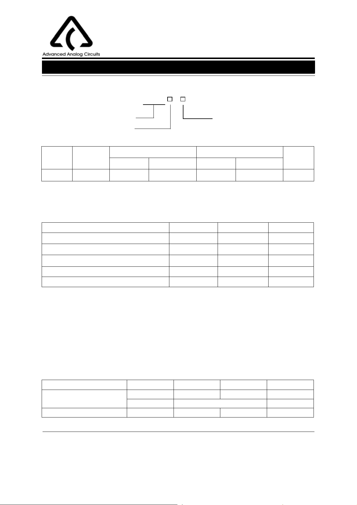
Ordering Information
AM5668
Circuit Type
-
E1: Lead Free
Blank: Tin Lead
Package
M28: HSOP-28
Package
HSOP-28
BCD Semiconductor's Pb-free products, as designated with "E1" suffix in the part number, are RoHS compliant.
Temperature
Range
0 to 70 ℃
Tin Lead Lead Free Tin Lead Lead Free
AM5668M28 AM5668M28-E1 AM5668M28 AM5668M28-E1 Tube
Part Number Marking ID
Absolute Maximum Ratings (TA=25oC) (Note 2)
Parameter Symbol Value Unit
Supply Voltage
Power Dissipation
Storage Temperature
ESD (Human Body Model) ESD 2000 V
ESD (Machine Model) ESD 200 V
V
T
CC1, 2
P
D
STG
13.5 V
1.7 (Note 3, 4) W
-55 to 150
Packing
Type
o
C
Note 2: Stresses greater than those listed under "Absolute Maximum Ratings" may cause permanent damage to
the device. These are stress ratings only, and functional operation of the device at these or any other conditions
beyond those indicated under "Recommended Operating Conditions" is not implied. Exposure to "Absolute Maximum Ratings" for extended periods may affect device reliability.
Note 3:
a. When mounted on a 70mmx70mmx1.6mm glass epoxy board.
b. Reduced by 13.6mW for each increase in T
of 1oC over 25oC.
A
Note 4: Do not exceed PD and SOA and TJ=150oC values.
Recommended Operating Conditions (TA=25oC)
Parameter Symbol Min Max Unit
Supply Voltage
Operating Temperature T
Sep. 2005 Rev. 1. 2
V
CC1
V
CC2
A
5
4.3 13.2 V
4.3 to V
CC1
070
V
o
C
BCD Semiconductor Manufacturing Limited
 Loading...