Low-Power Off-line Primary Side Regulation Controller AP3772
Advance Datasheet
General Description
The AP3772 is a high performance AC/DC power
supply controller for battery charger and adapter
applications. The device uses Pulse Frequency
Modulation (PFM) method to build discontinuous
conduction mode (DCM) flyback power supplies.
The AP3772 provides accurate constant voltage,
constant current (CV/CC) regulation without
requiring an opto-coupler and the secondary control
circuitry. It also eliminates the need of loop
compensation circuitry while maintaining good
stability. The AP3772 can achieve excellent
regulation and high average efficiency, yet meets
no-load consumption less than 30mW. It can also
achieve excellent dynamic performance while
maintaining 30mW standby power with AP4340.
The AP3772 has a built-in fixed cable voltage drop
compensation function. The magnitude of the cable
compensation voltage is set as 6%, 3% and 0 of the
rated output voltage respectively to meet various
cables with different length and gauge. It also has an
adjustable built-in line compensation function to
achieve tight CC.
The AP3772 is available in SOT-23-6 package.
Features
• Primary Side Control for Tight Constant Current
and Constant Voltage
• 30mW No-load Input Power
• Excellent Dynamic Performance with AP4340
• Bipolar Junction Transistor (BJT) Driving
• Proprietary Adjustable Line Compensation for
CC Variation
• Constant and Built-in 6%, 3% and No Cable
Voltage Drop Compensation
• Enhanced Audio Noise Suppression
• Open Circuit Protection
• Over Voltage Protection
• Short Circuit Protection
• SOT-23-6 package
Applications
• Adapters/Chargers for Cell/cordless Phones,
PDAs, MP3 and Other Portable Devices
• LED Driver
• Standby and Auxiliary Power Supplies
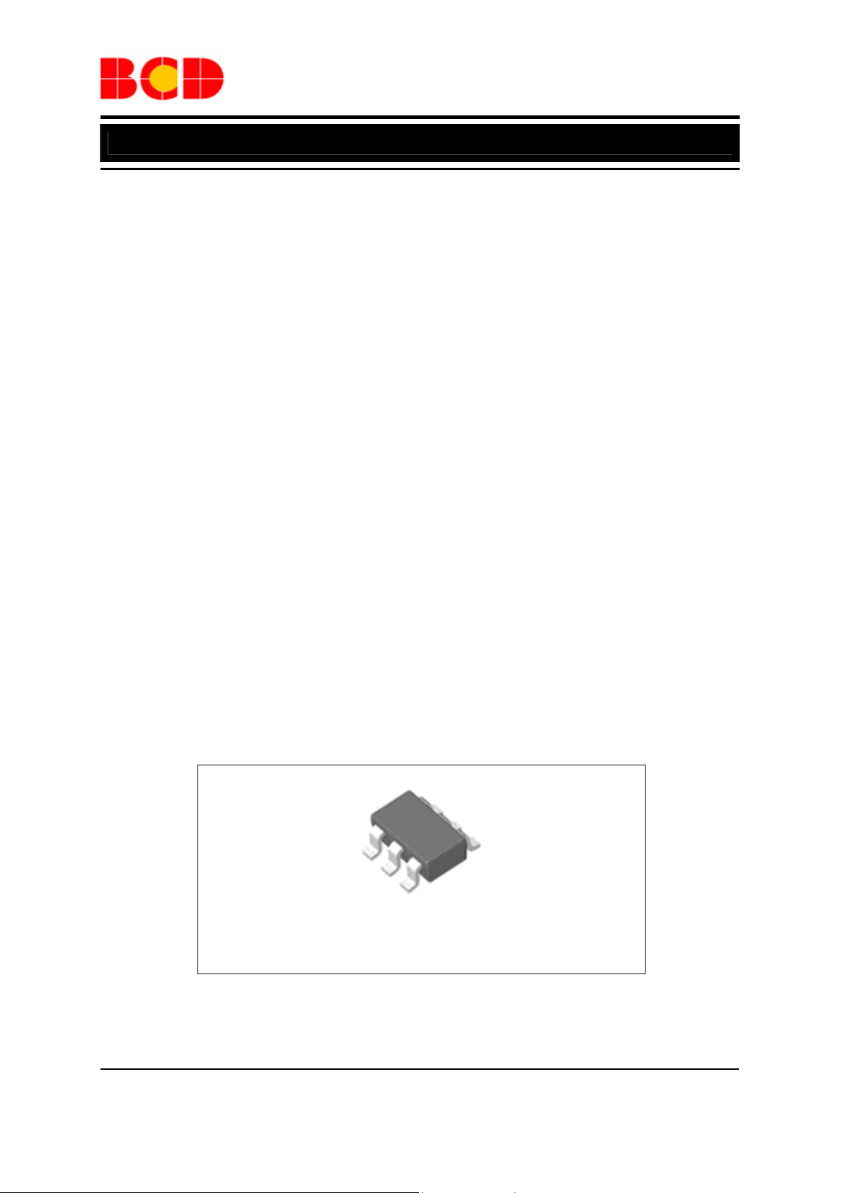
Figure 1. Package Type of AP3772
SOT-23-6
Dec. 2011 Rev. 1. 0 BCD Semiconductor Manufacturing Limited
1

Advance Datasheet
Low-Power Off-line Primary Side Regulation Controller AP3772
Pin Configuration
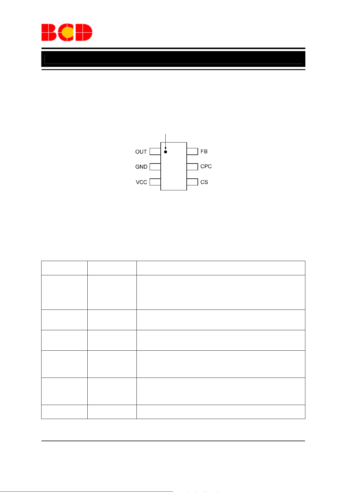
K6 Package
(SOT-23-6)
Pin 1 Mark
1
2
34
Figure 2. Pin Configuration of AP3772 (Top View)
6
5
Pin Description
Pin Number Pin Name Function
The OUT pin is used to turn on and turn off the power switch. When
turning on the power switch, the OUT pin will output 30mA source
1 OUT
2 GND
3 VCC
4 CS
5 CPC
6 FB
current to support the base current of the power BJT. When turning
off the power switch, the resistance between the OUT and GND will
become to 5Ω
The GND pin is the ground of the IC. When the power BJT is turned
off, a fast reverse sinking current to the gate of BJT will flow out
from this pin. Attention should be paid to in the PCB layout
The VCC pin supplies the power for the IC. In order to get the
correct operation of the IC, a capacitor with low ESR should be
placed as close as possible to the VCC pin
The CS is the current sense pin of the IC. The IC will turn off the
power BJT according to the voltage on the CS pin. When the power
BJT is on, a current is output from the CS pin which is proportional
to the line voltage to realize the function of line compensation
A capacitor more than 10nF should be connected to this pin. The
voltage of CPC pin is linear to load of the system and it is used for
the functions of cable voltage drop compensation and audio noise
suppression
The CV and CC regulation are realized based on the voltage
sampling of this pin
Dec. 2011 Rev. 1. 0 BCD Semiconductor Manufacturing Limited
2

Advance Datasheet
Low-Power Off-line Primary Side Regulation Controller AP3772
Functional Block Diagram
VCC
3
FB
UVLO
6
0.1V
COMP
PFM
OVP
&
OCKP
Tonsec
Detector
PRO
T
ONS
Regulator
&
Bias
UVLO
CS
V
FB
Line
Compensation
4
T
ONS
Dynamic
Response
Constant Voltage
EA
V
REF1
V
REF2
Constant Current
Control
Control
Peak Current
Control & LEB
Audio noise
Suppression
Cable
Compensation
Q
R
S
Shutdown
Pre_Shutdown
Q
R
S
CV_
CC_
CC
Pro
Dyn
ctrl
ctrl
_ctrl
PFM
Driver
1
OUT
2
GND
5
CPC
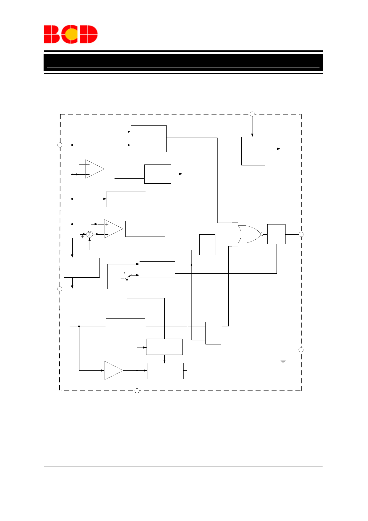
Figure 3. Functional Block Diagram of AP3772
Dec. 2011 Rev. 1. 0 BCD Semiconductor Manufacturing Limited
3

Advance Datasheet
Low-Power Off-line Primary Side Regulation Controller AP3772
Ordering Information
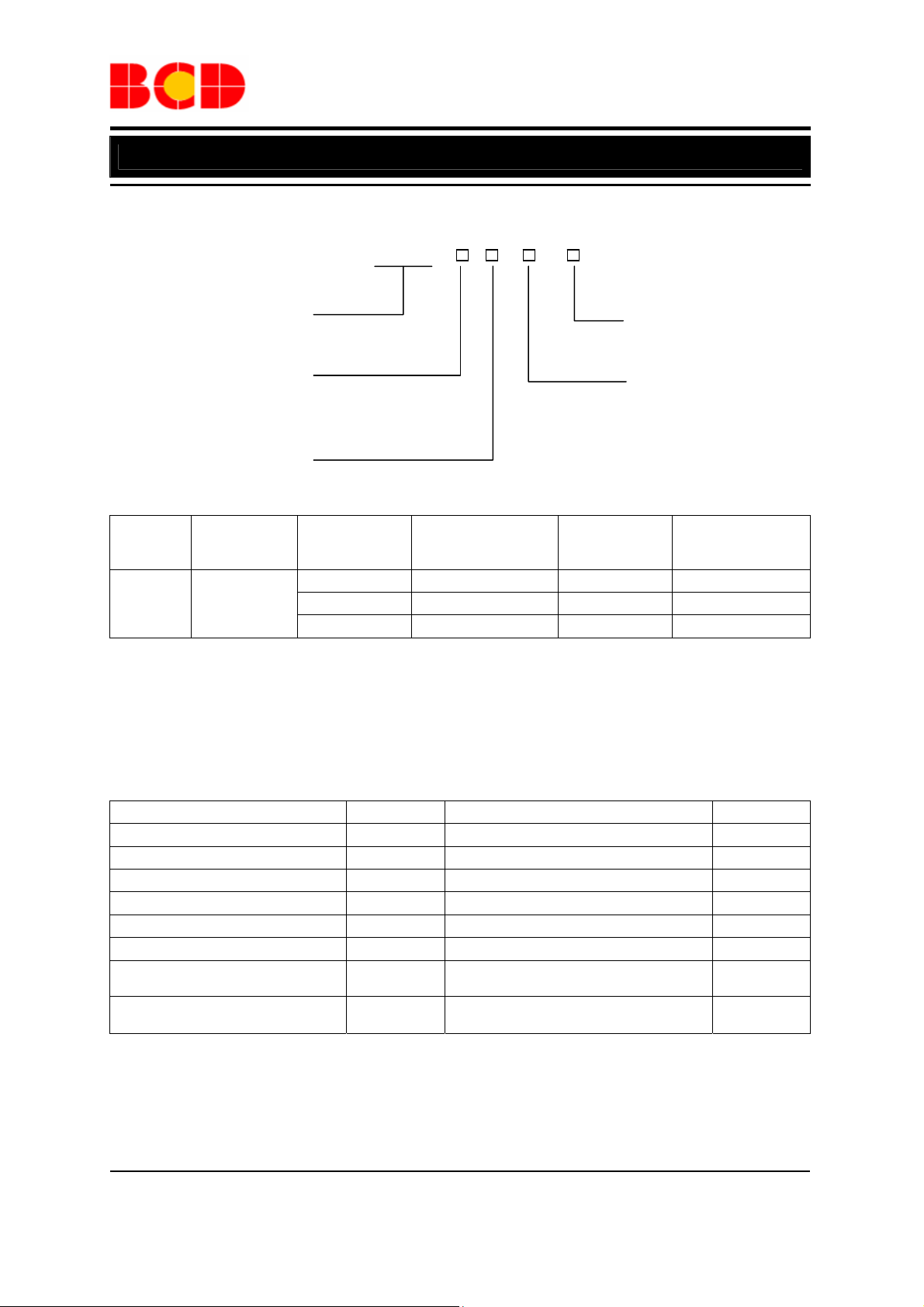
AP3772 -
Circuit Type
G1: Green
Cable Compensation Voltage
A: 6%
B: 3%
C: 0
Package
K6: SOT-23-6
TR: Tape & Reel
Package
SOT-23-6
BCD Semiconductor's Pb-free products, as designated with "G1" suffix in the part number, are RoHS compliant
and green.
Temperature
Range
-40 to 85°C
Cable
Compensation
Voltage
6% AP3772AK6TR-G1 GKA Tape & Reel
3% AP3772BK6TR-G1 GKB Tape & Reel
0 AP3772CK6TR-G1 GKC Tape & Reel
Part Number Marking ID Packing Type
Absolute Maximum Ratings (Note 1)
Parameter Symbol Value Unit
Supply Voltage VCC -0.3 to 30 V
CS, CPC to GND -0.3 to 7 V
FB Input Voltage VFB -40 to 10 V
Source Current at OUT Pin I
Operating Junction Temperature TJ 150 ºC
Storage Temperature T
Lead Temperature (Soldering, 10
sec)
Thermal Resistance (Junction to
Ambient)
Internally Limited A
SOURCE
-65 to 150 ºC
STG
T
300 ºC
LEAD
θ
JA
200 ºC/W
Note 1: Stresses greater than those listed under “Absolute Maximum Ratings” may cause permanent damage to
the device. These are stress ratings only, and functional operation of the device at these or any other conditions
beyond those indicated under “Recommended Operating Conditions” is not implied. Exposure to “Absolute
Maximum Ratings” for extended periods may affect device reliability.
Dec. 2011 Rev. 1. 0 BCD Semiconductor Manufacturing Limited
4
 Loading...