


BCD AP3211KTR-G1 Schematic [ru]
1.4MHz, 1.5A ASYNCHRONOUS DC-DC BUCK CONVERTER AP3211
Data Sheet
General Description
The AP3211 is a 1.4MHz fixed frequency, current
mode, PWM buck (step-down) DC-DC converter,
capable of driving a 1.5A load with high efficiency,
excellent line and load regulation. The device
integrates N-channel power MOSFET switch with
low on-resistance. Current mode control provides fast
transient response and cycle-by-cycle current limit.
A standard series of inductors are available from
several different manufacturers optimized for use
with the AP3211. This feature greatly simplifies the
design of switch-mode power supplies.
The AP3211 is available in SOT-23-6 package.
Features
• Input Voltage Range: 4.5V to 18V
• Output Voltage Adjustable from 0.81V to 15V
• Fixed 1.4MHz Frequency
• High Efficiency: up to 92%
• Output Current: 1.5A
• Current Mode Control
• Built-in Over Current Protection
• Built-in Thermal Shutdown Function
• Built-in UVLO Function
• Built-in Over Voltage Protection
• Built-in Soft-start
Applications
• LCD TV
• DPF
• Portable DVD
SOT-23-6
Figure 1. Package Type of AP3211
Apr. 2013 Rev. 1. 4 BCD Semiconductor Manufacturing Limited
1
Data Sheet
1.4MHz, 1.5A ASYNCHRONOUS DC-DC BUCK CONVERTER AP3211
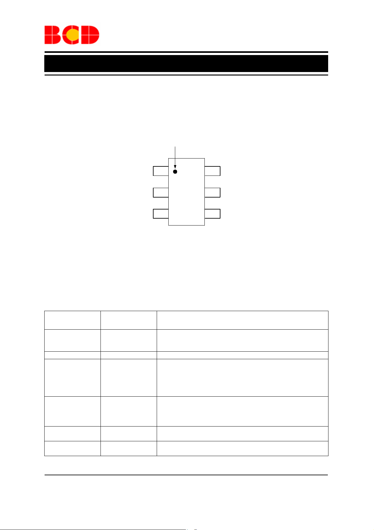
Pin Configuration
K Package
(SOT-23-6)
Pin 1 Mark
6
BS
1
SW
GND
2
5
IN
FB
34
EN
Figure 2. Pin Configuration of AP3211 (Top View)
Pin Description
Pin Number Pin Name Function
Bootstrap pin. A bootstrap capacitor is connected between the
1 BS
2 GND Ground pin
3 FB
4 EN
5 IN
6 SW
BS pin and SW pin. The voltage across the bootstrap capacitor
drives the internal high-side NMOS switch
Feedback pin. This pin is connected to an external resistor
divider to program the system output voltage. When V
20% of the nominal regulation value of 0.81V, the OVP is
triggered. When V
to realize short circuit protection
Control input pin. Forcing this pin above 1.5V enables the IC.
Forcing this pin below 0.4V shuts down the IC. When the IC is
in shutdown mode, all functions are disabled to decrease the
supply current below 1μA
Supply input pin. A capacitor should be connected between the
IN pin and GND to keep the DC input voltage constant
Power switch output pin. This pin is connected to the inductor
and bootstrap capacitor
<0.25V, the oscillator frequency is lowered
FB
exceeds
FB
Apr. 2013 Rev. 1. 4 BCD Semiconductor Manufacturing Limited
2
Data Sheet
1.4MHz, 1.5A ASYNCHRONOUS DC-DC BUCK CONVERTER AP3211
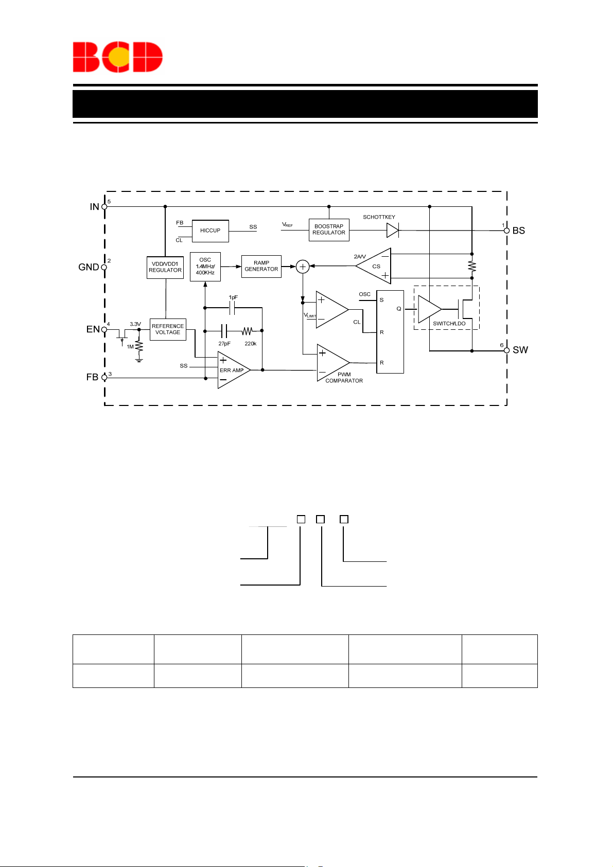
Functional Block Diagram
Figure 3. Functional Block Diagram of AP3211
Ordering Information
AP3211 -
Circuit Type G1: Green
Package TR: Tape & Reel
K: SOT-23-6
Package
SOT-23-6
Temperature
Range
-40 to 85°C
Part Number Marking ID
AP3211KTR-G1 GCI Tape & Reel
BCD Semiconductor's Pb-free products, as designated with "G1" suffix in the part number, are RoHS compliant
and green.
Packing
Type
Apr. 2013 Rev. 1. 4 BCD Semiconductor Manufacturing Limited
3
Data Sheet
1.4MHz, 1.5A ASYNCHRONOUS DC-DC BUCK CONVERTER AP3211
Absolute Maximum Ratings (Note 1)
Parameter Symbol Value Unit
Input Pin Voltage VIN -0.3 to 20 V
EN Pin Voltage VEN -0.3 to VIN+0.3 V
SW Pin Voltage VSW 21 V
Bootstrap Pin Voltage VBS -0.3 to VSW+6 V
Feedback Pin Voltage VFB -0.3 to 6V V
Thermal Resistance
Operating Junction Temperature TJ 150 ºC
Storage Temperature T
Lead Temperature (Soldering,
10sec)
ESD (Human Body Model) 2000 V
ESD (Machine Model) 200 V
Note 1: Stresses greater than those listed under “Absolute Maximum Ratings” may cause permanent damage to
the device. These are stress ratings only, and functional operation of the device at these or any other conditions
beyond those indicated under “Recommended Operating Conditions” is not implied. Exposure to “Absolute
Maximum Ratings” for extended periods may affect device reliability.
θ
JA
-65 to 150 ºC
STG
260 ºC
T
LEAD
220 ºC/W
Recommended Operating Conditions
Parameter Symbol Min Max Unit
Input Voltage VIN 4.5 18 V
Maximum Output Current I
Operating Ambient Temperature TA -40 85 ºC
OUT (MAX)
1.5 A
Apr. 2013 Rev. 1. 4 BCD Semiconductor Manufacturing Limited
4
Data Sheet
1.4MHz, 1.5A ASYNCHRONOUS DC-DC BUCK CONVERTER AP3211
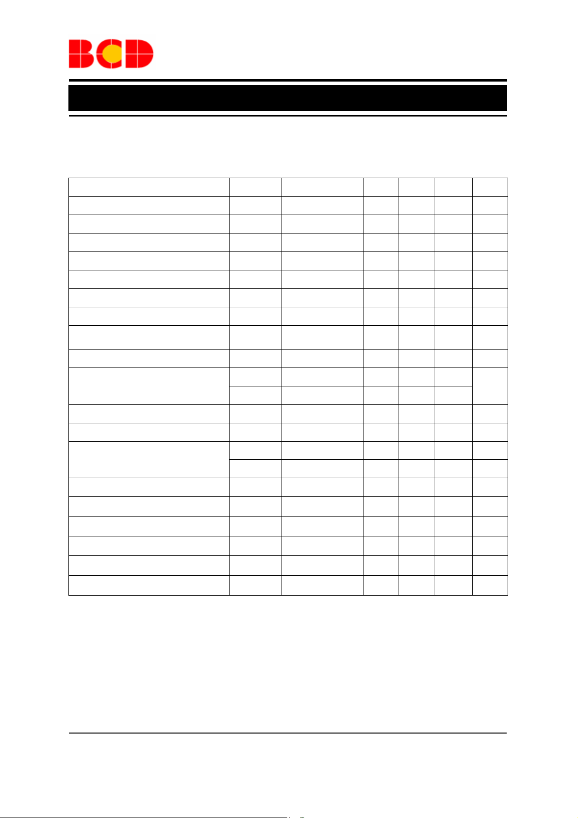
Electrical Characteristics
VIN=VEN=12V, V
Parameter Symbol Conditions Min Typ Max Unit
Input Voltage VIN 4.5 18 V
Quiescent Current IQ VFB=0.9V 0.8 1.1 mA
=3.3V, TA=25ºC, unless otherwise specified.
OUT
Shutdown Supply Current I
Feedback Voltage V
Feedback Over Voltage Threshold V
Feedback Bias Current IFB VFB=0.85V -0.1 0.1
Switch On-resistance R
Switch Leakage Current I
Switch Current Limit I
EN Pin Threshold
Input UVLO Threshold V
Input UVLO Hysteresis V
Oscillator Frequency
Max. Duty Cycle D
Min. Duty Cycle D
VEN=0V 0.1 1.0
SHDN
FB
0.972 V
FBOV
0.785 0.810 0.835 V
μA
μA
ISW=1A
DSON
=18V,
V
IN
LEAK
LIM
V
1.5
ENH
V
0.4
ENL
UVLO
0.2 V
HYS
f
1.1 1.4 1.7 MHz
OSC1
f
Short Circuit 460 kHz
OSC2
VFB=0.6V 90 %
MAX
VFB=0.9V 0 %
MIN
=0V
V
EN
1.8 2.4 A
V
Rising 3.3 3.8 4.3 V
IN
0.35
0.1 10
Ω
μA
V
Minimum On Time tON 100 ns
Thermal Shutdown T
Thermal Shutdown Hysteresis T
Soft-start Time tSS 200
Note 2: R
DSON , tON, TOTSD, THYS
and t
are guaranteed by design.
SS
160 ºC
OTSD
20 ºC
HYS
μs
Apr. 2013 Rev. 1. 4 BCD Semiconductor Manufacturing Limited
5