BCD AP2114H-1.2TRG1, AP2114H-1.5TRG1, AP2114H-1.8TRG1, AP2114H-2.5TRG1, AP2114H-3.3TRG1 Schematic [ru]
...
1A LOW NOISE CMOS LDO REGULATOR WITH ENABLE AP2114
Data Sheet
General Description
The AP2114 is CMOS process low dropout linear
regulator with enable function, the regulator delivers
a guaranteed 1A (Min) continuous load current.
The AP2114 features low power consumption.
The AP2114 is available in 1.2V, 1.5V, 1.8V, 2.5V
and 3.3V regulator output and 0.8V to 5V adjustable
output, and available in excellent output accuracy
±1.5%, it is also available in an excellent load
regulation and line regulation performance.
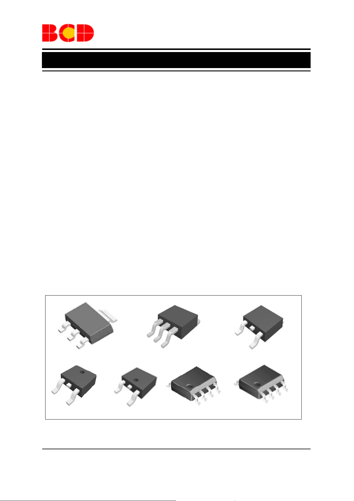
The AP2114 is available in standard packages of
SOT-223, TO-252-2
TO-263-3, SOIC-8 and PSOP-8.
(1), TO-252-2 (3), TO-252-2 (4),
Features
• Output Voltage Accuracy: ±1.5%
• Output Current: 1A (Min)
• Fold-back Short Current Protection: 50mA
• Low Dropout Voltage (3.3V): 450mV (Typ)
@I
=1A
OUT
• Stable with 4.7μF Flexible Cap: Ceramic,
Tantalum and Aluminum Electrolytic
• Excellent Line Regulation: 0.02%/V (Typ),
0.1%/V (Max) @ I
• Excellent Load Regulation: 0.2%A (Typ) @
I
=1mA to 1A
OUT
• Low Quiescent Current: 60μA (1.2V/1.5V/1.8V
/2.5V/ADJ)
• Low Output Noise: 30μV
• PSRR: 68dB @ Freq=1KHz (1.2V/1.5V/1.8V
/ADJ)
• OTSD Protection
• Operating Temperature Range: -40°C to 85°C
• ESD: MM 400V, HBM 4000V
OUT
=30mA
RMS
Applications
• LCD Monitor
• LCD TV
• STB
SOT-223 TO-263-3 TO-252-2 (1)
TO-252-2 (3) TO-252-2 (4) SOIC-8 PSOP-8
Figure 1. Package Types of AP2114
Jan. 2013 Rev. 2. 2 BCD Semiconductor Manufacturing Limited
1
Data Sheet
1A LOW NOISE CMOS LDO REGULATOR WITH ENABLE AP2114
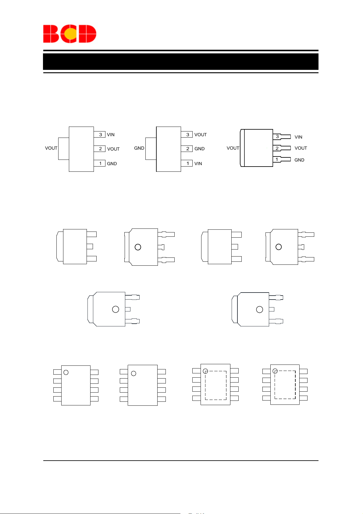
Pin Configuration
H/HA Package S Package
(SOT-223) (TO-263-3)
H HA
D/DA Package
D DA
(TO-252-2 (1)) (TO-252-2 (3)) (TO-252-2 (1)) (TO-252-2 (3))
3
VIN
2
VOUTVOUT
1
GND
VOUT
3
VIN
VOUT
2
1
GND
GND
VOUT
3
GND
VIN
GND
2
1
3
2
1
(TO-252-2 (4)) (TO-252-2 (4))
3
VIN
3
VOUT
VOUT
2
VOUT
1
GND
GND
2
GND
1
VIN
M Package MP Package
(SOIC-8) (PSOP-8)
GND
1
2
VOUT
3
GND
VIN
4
8
EN
GND
7
6
GND
GND
5
VIN
GND
EN
VOUT
GNDGND
ADJ
GND
GND
VOUT
GND
VIN
2
3
4
1
2
3
4
8
7
6
5
1
8
EN
7
GND
6
GND
GND
5
VIN
GND
EN
1
2
3
4
For Fixed Versions For Adjustable Version For Fixed Versions For Adjustable Version
Figure 2. Pin Configuration of AP2114 (Top View)
VOUT
GND
VIN
8
VOUT
GNDGND
7
ADJ
6
5
GND
Jan. 2013 Rev. 2. 2 BCD Semiconductor Manufacturing Limited
2
Data Sheet
1A LOW NOISE CMOS LDO REGULATOR WITH ENABLE AP2114
Pin Descriptions
SOT-223 (H),
TO-263-3,
TO-252-2 (1) (D)
TO-252-2 (3) (D)
TO-252-2 (4) (D)
1 2 1, 3, 5, 6, 7 2, 3, 5, 7 GND Ground
2 3 2 8 VOUT Regulated Output
3 1 4 1 VIN Input Voltage Pin
6 ADJ Adjust Output
Pin Number
SOT-223 (HA),
TO-252-2 (1) (DA)
TO-252-2 (3) (DA)
TO-252-2 (4) (DA)
SOIC-8,
PSOP-8
(Fixed)
8 4 EN
SOIC-8,
PSOP-8
(ADJ)
Pin
Name
Chip Enable, H–Normal
Work, L– Shutdown Output
Function
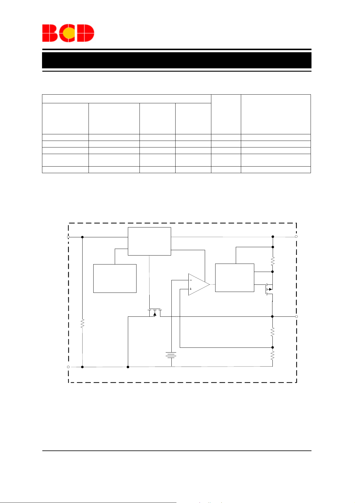
Functional Block Diagram
(8)
EN
Thermal
Shutdown
3MΩ
GND
1 ( 1, 3, 5, 6, 7 )
A (B)
A: SOT-223 , TO -263 -3, TO-252 -2 (1)/(3
{2}
{C}
(H)
B: SOIC-8, PSOP-8
C: SOT-223 ,
(HA)
Shutdown
Logic
TO-252-2 (1)/(3
V
REF
)/(4)
(DA)
Foldback
Current Limit
(D))/(
4)
For Fixed Versions
Jan. 2013 Rev. 2. 2 BCD Semiconductor Manufacturing Limited
3
3 (4)
2 (2)
{1}
VIN
{3}
VOUT
Data Sheet
1A LOW NOISE CMOS LDO REGULATOR WITH ENABLE AP2114
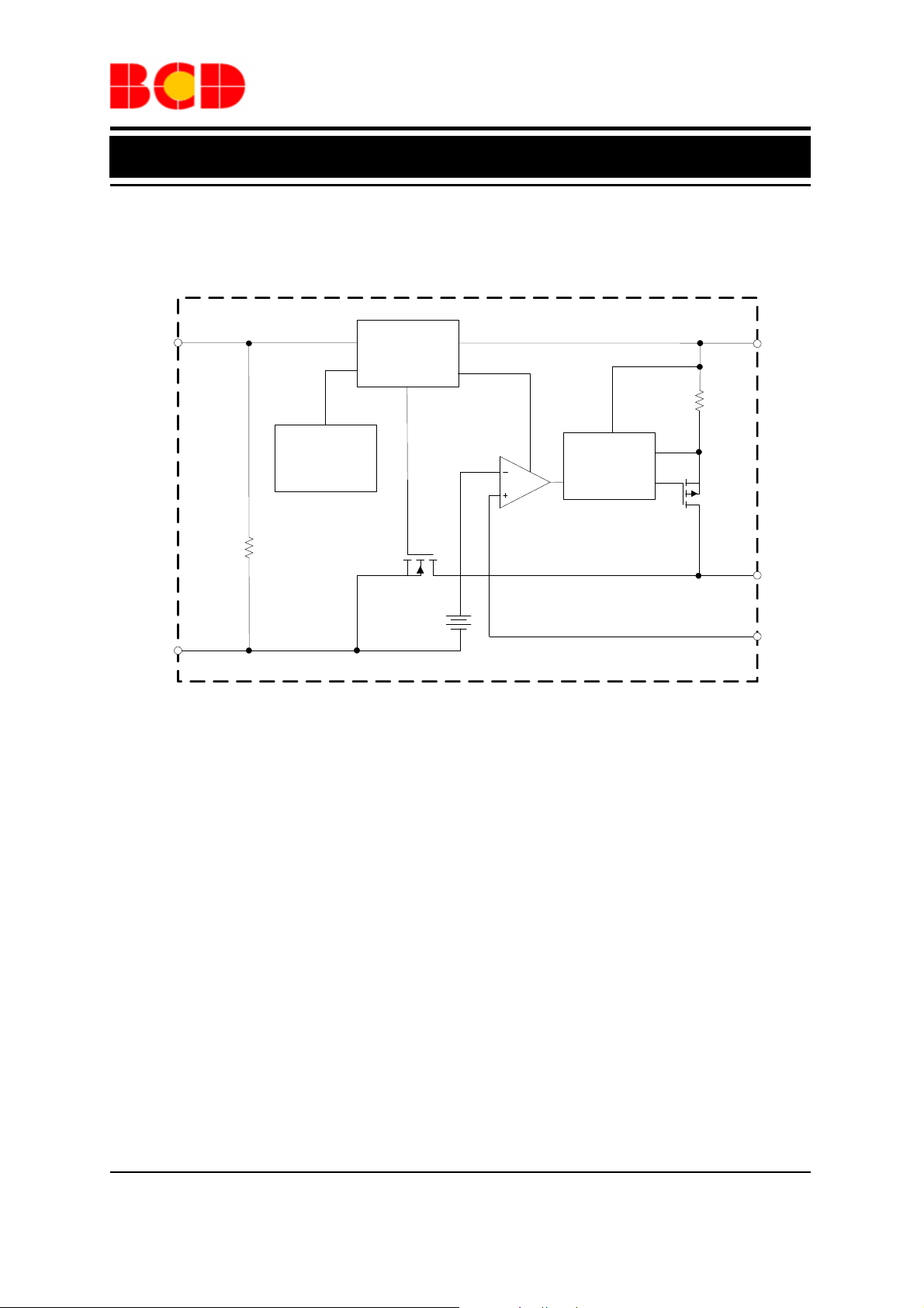
Functional Block Diagram (Continued)
EN
4
Shutdown
Logic
1
VIN
Thermal
Shutdown
Foldback
Current Limit
3 Ω
M
8
VOUT
V
GND
2, 3, 5, 7
REF
6
ADJ
SOIC-8, PSOP-8
For ADJ Version
Figure 3. Functional Block Diagram of AP2114
Jan. 2013 Rev. 2. 2 BCD Semiconductor Manufacturing Limited
4
Data Sheet
1A LOW NOISE CMOS LDO REGULATOR WITH ENABLE AP2114
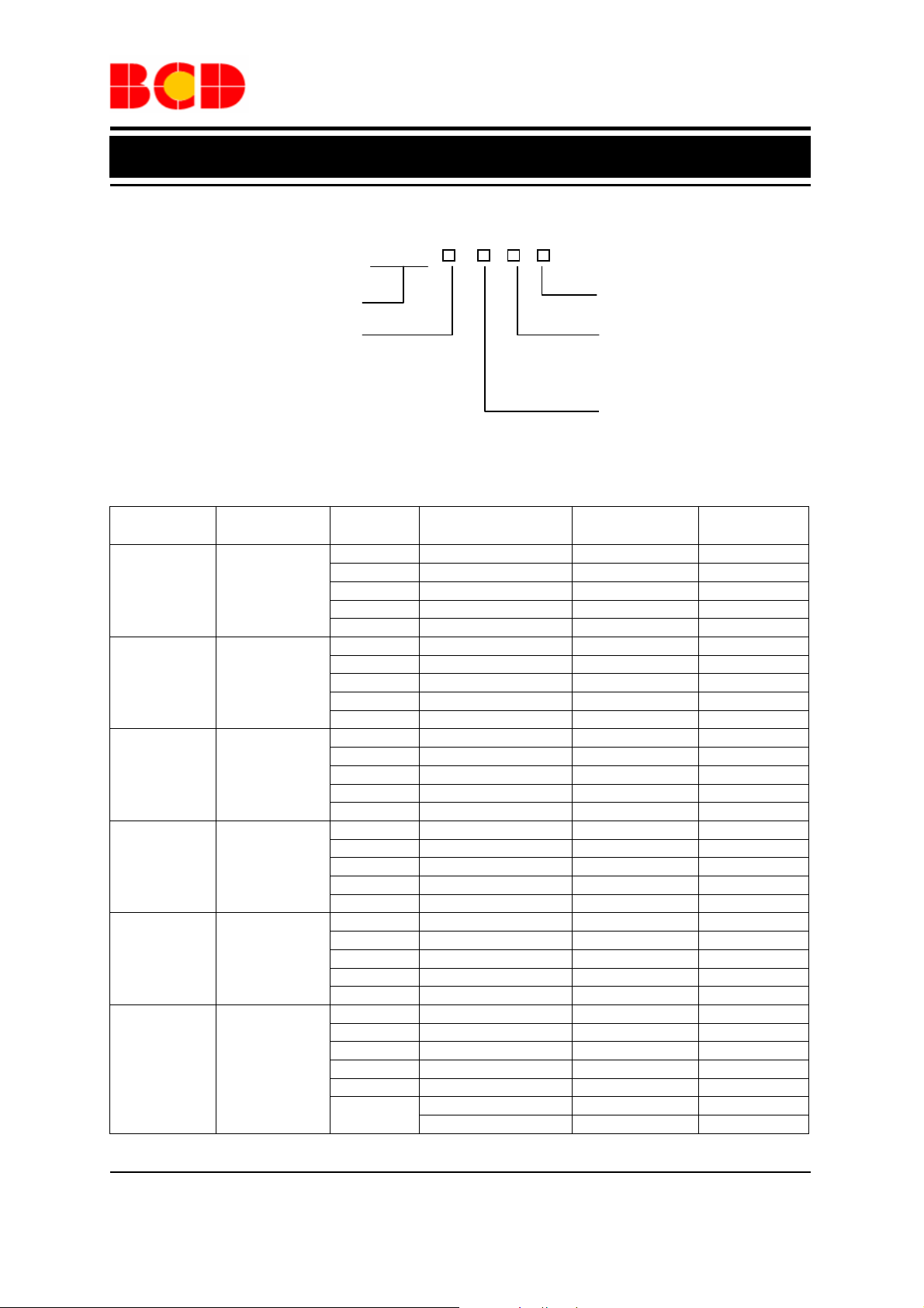
Ordering Information
AP2114 -
Circuit Type G1: Green
Package
SOT-223
SOT-223
TO-252-2 (1)/
TO-252-2 (3)/
TO-252-2 (4)
TO-252-2 (1)/
TO-252-2 (3)/
TO-252-2 (4)
TO-263-3
SOIC-8
Package
H/HA: SOT-223
D/DA: TO-252-2 (1)/(3)/(4)
S: TO-263-3
M: SOIC-8
MP: PSOP-8
Temperature
Range
-40 to 85°C
-40 to 85°C
-40 to 85°C
-40 to 85°C
-40 to 85°C
-40 to 85°C
Output
Voltage
1.2V (H) AP2114H-1.2TRG1 GH12C Tape & Reel
1.5V (H) AP2114H-1.5TRG1 GH16G Tape & Reel
1.8V (H) AP2114H-1.8TRG1 GH12D Tape & Reel
2.5V (H) AP2114H-2.5TRG1 GH14C Tape & Reel
3.3V (H) AP2114H-3.3TRG1 GH12E Tape & Reel
1.2V (HA) AP2114HA-1.2TRG1 GH13B Tape & Reel
1.5V (HA) AP2114HA-1.5TRG1 GH16H Tape & Reel
1.8V (HA) AP2114HA-1.8TRG1 GH14D Tape & Reel
2.5V (HA) AP2114HA-2.5TRG1 GH14E Tape & Reel
3.3V (HA) AP2114HA-3.3TRG1 GH14F Tape & Reel
1.2V (D) AP2114D-1.2TRG1 AP2114D-1.2G1 Tape & Reel
1.5V (D) AP2114D-1.5TRG1 AP2114D-1.5G1 Tape & Reel
1.8V (D) AP2114D-1.8TRG1 AP2114D-1.8G1 Tape & Reel
2.5V (D) AP2114D-2.5TRG1 AP2114D-2.5G1 Tape & Reel
3.3V (D) AP2114D-3.3TRG1 AP2114D-3.3G1 Tape & Reel
1.2V (DA) AP2114DA-1.2TRG1 AP2114DA-1.2G1 Tape & Reel
1.5V (DA) AP2114DA-1.5TRG1 AP2114DA-1.5G1 Tape & Reel
1.8V (DA) AP2114DA-1.8TRG1 AP2114DA-1.8G1 Tape & Reel
2.5V (DA) AP2114DA-2.5TRG1 AP2114DA-2.5G1 Tape & Reel
3.3V (DA) AP2114DA-3.3TRG1 AP2114DA-3.3G1 Tape & Reel
1.2V AP2114S-1.2TRG1 AP2114S-1.2G1 Tape & Reel
1.5V AP2114S-1.5TRG1 AP2114S-1.5G1 Tape & Reel
1.8V AP2114S-1.8TRG1 AP2114S-1.8G1 Tape & Reel
2.5V AP2114S-2.5TRG1 AP2114S-2.5G1 Tape & Reel
3.3V AP2114S-3.3TRG1 AP2114S-3.3G1 Tape & Reel
1.2V AP2114M-1.2TRG1 2114M-1.2G1 Tape & Reel
1.5V AP2114M-1.5TRG1 2114M-1.5G1 Tape & Reel
1.8V AP2114M-1.8TRG1 2114M-1.8G1 Tape & Reel
2.5V AP2114M-2.5TRG1 2114M-2.5G1 Tape & Reel
3.3V AP2114M-3.3TRG1 2114M-3.3G1 Tape & Reel
ADJ
Part Number Marking ID
AP2114M-ADJG1 2114M-ADJG1 Tube
AP2114M-ADJTRG1 2114M-ADJG1 Tape & Reel
Blank: Tube
TR: Tape & Reel
1.2: Fixed Output 1.2V
1.5: Fixed Output 1.5V
1.8: Fixed Output 1.8V
2.5: Fixed Output 2.5V
3.3: Fixed Output 3.3V
ADJ: ADJ Output
Packing
Type
Jan. 2013 Rev. 2. 2 BCD Semiconductor Manufacturing Limited
5
Data Sheet
1A LOW NOISE CMOS LDO REGULATOR WITH ENABLE AP2114
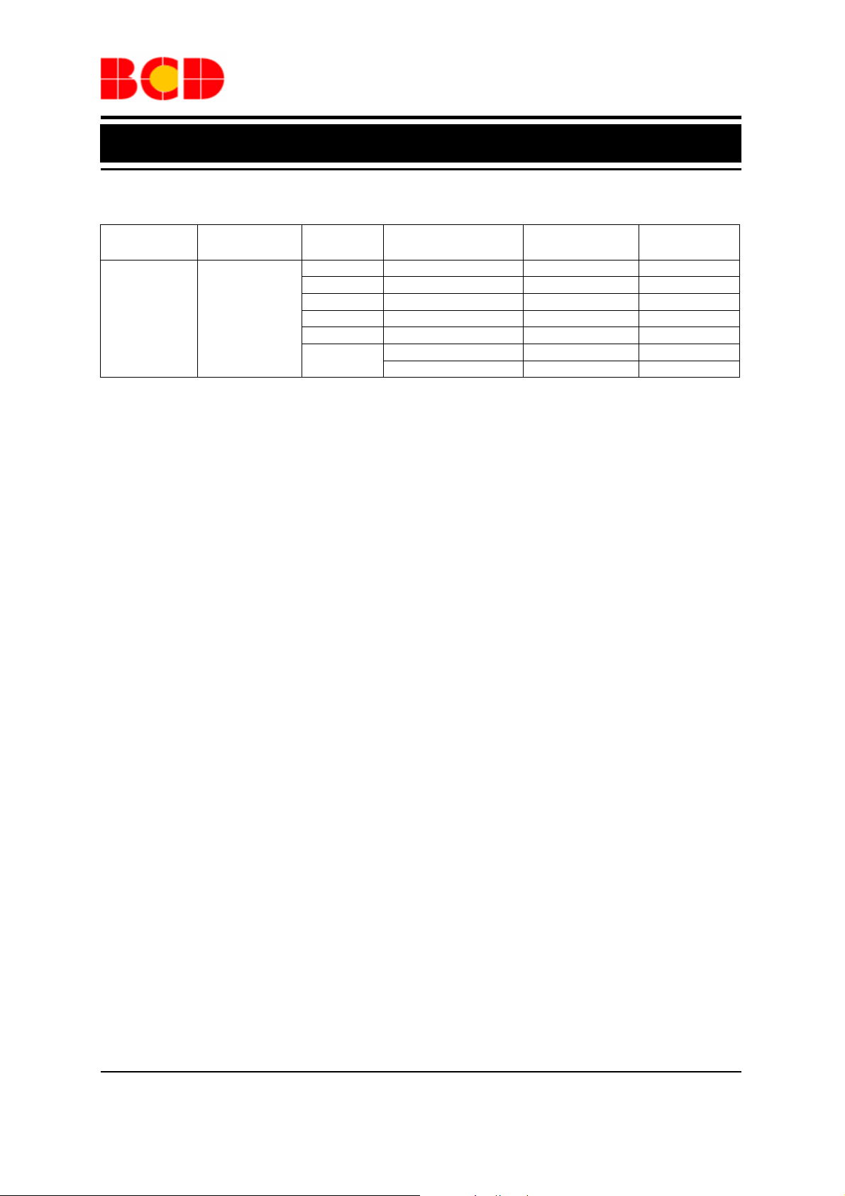
Ordering Information (Continued)
Package
PSOP-8
Temperature
Range
-40 to 85°C
BCD Semiconductor's Pb-free products, as designated with "G1" suffix in the part number, are RoHS compliant
and Green.
Output
Voltage
1.2V AP2114MP-1.2TRG1 2114MP-1.2G1 Tape & Reel
1.5V AP2114MP-1.5TRG1 2114MP-1.5G1 Tape & Reel
1.8V AP2114MP-1.8TRG1 2114MP-1.8G1 Tape & Reel
2.5V AP2114MP-2.5TRG1 2114MP-2.5G1 Tape & Reel
3.3V AP2114MP-3.3TRG1 2114MP-3.3G1 Tape & Reel
ADJ
Part Number Marking ID
AP2114MP-ADJG1 2114MP-ADJG1 Tube
AP2114MP-ADJTRG1 2114MP-ADJG1 Tape & Reel
Packing
Type
Jan. 2013 Rev. 2. 2 BCD Semiconductor Manufacturing Limited
6
Data Sheet
1A LOW NOISE CMOS LDO REGULATOR WITH ENABLE AP2114
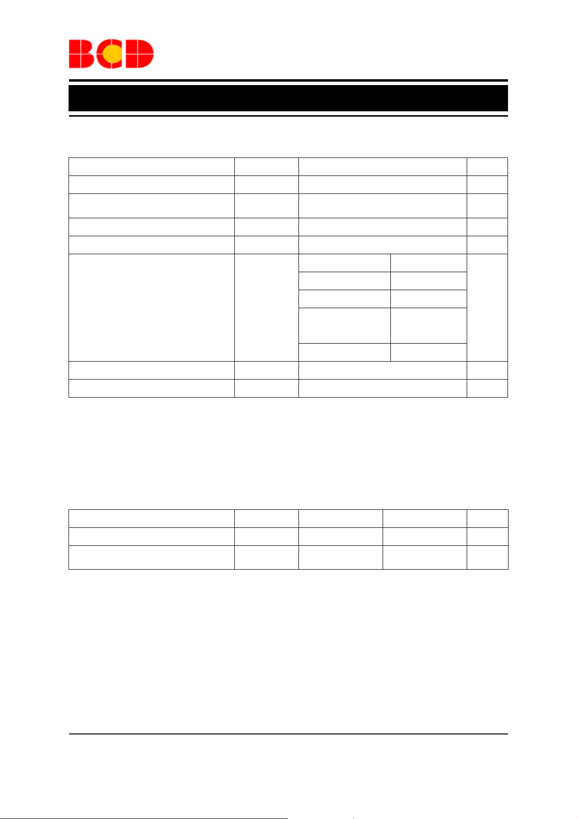
Absolute Maximum Ratings (Note 1)
Parameter Symbol Value Unit
Power Supply Voltage VIN 6.5 V
Operating Junction Temperature
Range
Storage Temperature Range T
150 ºC
T
J
-65 to 150 ºC
STG
Lead Temperature (Soldering, 10sec) T
Thermal Resistance (Junction to
Ambient)(No Heatsink)
ESD (Machine Model)
ESD (Human Body Model) 4000 V
260 ºC
LEAD
SOIC-8 144
PSOP-8 143
θ
JA
SOT-223 128
TO-252-2 (1)/
TO-252-2 (3)/
TO-252-2 (4)
TO-263-3 73
400 V
90
°C/W
Note 1: Stresses greater than those listed under “Absolute Maximum Ratings” may cause permanent damage to
the device. These are stress ratings only, and functional operation of the device at these or any other conditions
beyond those indicated under “Recommended Operating Conditions” is not implied. Exposure to “Absolute
Maximum Ratings” for extended periods may affect device reliability.
Recommended Operating Conditions
Parameter Symbol Min Max Unit
Supply Voltage VIN 2.5 6.0 V
Operating Ambient Temperature
Range
-40 85 °C
T
A
Jan. 2013 Rev. 2. 2 BCD Semiconductor Manufacturing Limited
7
n
N
Data Sheet
1A LOW NOISE CMOS LDO REGULATOR WITH ENABLE AP2114
Electrical Characteristics
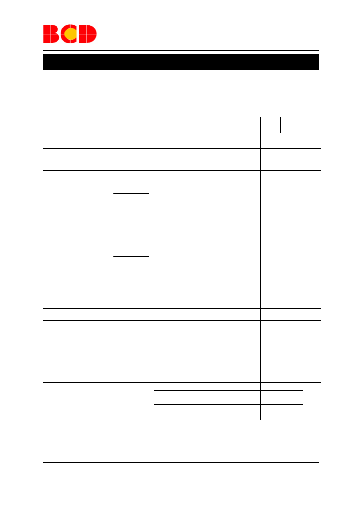
AP2114-1.2 Electrical Characteristics (Note 2)
(VIN=2.5V, CIN=4.7μF (Ceramic), C
ranges, unless otherwise specified (Note 3))
Parameter Symbol Test Conditions Min Typ Max Unit
=4.7μF (Ceramic), Typical T
OUT
= 25°C, Bold typeface applies over -40
A
O
C≤TA≤85OC
Output Voltage V
V
OUT
=2.5V, 1mA ≤ I
IN
OUT
≤ 30mA
V
OUT
×98.5%
1.2
V
OUT
×101.5%
V
Input Voltage VIN 6.0 V
Maximum Output Current I
Load Regulation
Line Regulation
OUT(MAX)
△V
△V
Dropout Voltage V
Quiescent Current IQ V
Power Supply Rejectio
Ratio
Output Voltage
△V
Temperature Coefficient
Short Current Limit I
RMS Output Noise V
VIN=2.5V, V
OUT/VOUT
OUT/VOUT
I△
OUT
V△
IN
I
DROP
VIN=2.5V, 1mA ≤ I
2.5V≤VIN≤6V, I
=1.0A 1200 1300 mV
OUT
=2.5V, I
IN
Ripple 1Vp-p
PSRR
OUT/VOUT
T△
SHORT
NOISE
VIN=2.5V,
I
=100mA
OUT
I
=30mA, TA =-40°C to 85°C
OUT
V
=0V 50 mA
OUT
10Hz ≤ f ≤100kHz (No Load) 30
=1.182V to 1.218V 1 A
OUT
≤1A 0.2 1 %/A
OUT
=30mA -0.1 0.02 0.1 %/V
OUT
=0mA 60 75
OUT
f=100Hz 68
f=1KHz 68
±30
μA
dB
ppm/°C
μV
RMS
VEN High Voltage VIH Enable logic high, regulator on 1.5
V
VEN Low Voltage VIL Enable logic low, regulator off 0.4
Standby Current I
V
STD
=2.5V, VEN in OFF mode 0.01 1.0
IN
μA
Start-up Time t
EN Pull Down Resistor
V
Discharge Resistor
OUT
Thermal Shutdown
Temperature
Thermal Shutdown
Hysteresis
R
T
T
HYOTSD
S
R
3.0
PD
Set EN pin at Low 60
DCHG
160
OTSD
o Load 20
25
μs
MΩ
Ω
°C
SOIC-8 74.6
Thermal Resistance
(Junction to Case)
θ
JC
PSOP-8 43.7
SOT-223 50.9
°C/W
TO-252-2 (1) /(3) /(4) 35
TO-263-3 22
Note 2: To prevent the Short Circuit Current protection feature from being prematurely activated, the input
voltage must be applied before a current source load is applied.
Note 3: Production testing at T
Jan. 2013 Rev. 2. 2 BCD Semiconductor Manufacturing Limited
=25°C. Over temperature specifications guaranteed by design only.
A
8

n
N
Data Sheet
1A LOW NOISE CMOS LDO REGULATOR WITH ENABLE AP2114
Electrical Characteristics (Continued)
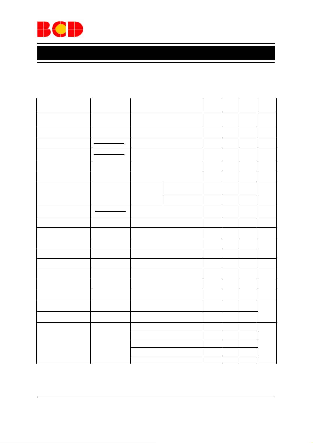
AP2114-1.5 Electrical Characteristics (Note 2)
(VIN=2.5V, CIN=4.7μF (Ceramic), C
ranges, unless otherwise specified (Note 3))
Parameter Symbol Test Conditions Min Typ Max Unit
=4.7μF (Ceramic), Typical T
OUT
= 25°C, Bold typeface applies over -40
A
O
C≤TA≤85OC
Output Voltage V
V
OUT
=2.5V, 1mA ≤ I
IN
OUT
≤ 30mA
V
OUT
×98.5%
1.5
V
OUT
×101.5%
V
Input Voltage VIN 6.0 V
Maximum Output Current I
Load Regulation
Line Regulation
OUT(MAX)
△V
△V
Dropout Voltage V
Quiescent Current IQ V
Power Supply Rejectio
Ratio
Output Voltage
△V
Temperature Coefficient
Short Current Limit I
RMS Output Noise V
VIN=2.5V, V
OUT/VOUT
OUT/VOUT
I△
OUT
V△
IN
I
DROP
VIN=2.5V, 1mA ≤ I
2.5V≤VIN≤6V, I
=1.0A 800 1000 mV
OUT
=2.5V, I
IN
Ripple 1Vp-p
PSRR
OUT/VOUT
T△
SHORT
NOISE
VIN=2.5V,
I
=100mA
OUT
I
=30mA, TA =-40°C to 85°C
OUT
V
=0V 50 mA
OUT
10Hz ≤ f ≤100kHz (No Load) 30
=1.478V to 1.523V 1 A
OUT
≤1A 0.2 1 %/A
OUT
=30mA -0.1 0.02 0.1 %/V
OUT
=0mA 60 75
OUT
f=100Hz 68
f=1KHz 68
±30
μA
dB
ppm/°C
μV
RMS
VEN High Voltage VIH Enable logic high, regulator on 1.5
V
VEN Low Voltage VIL Enable logic low, regulator off 0.4
Standby Current I
V
STD
=2.5V, VEN in OFF mode 0.01 1.0
IN
μA
Start-up Time t
EN Pull Down Resistor
V
Discharge Resistor
OUT
Thermal Shutdown
Temperature
Thermal Shutdown
Hysteresis
R
T
T
HYOTSD
S
R
3.0
PD
Set EN pin at Low 60
DCHG
160
OTSD
o Load 20
25
μs
MΩ
Ω
°C
SOIC-8 74.6
Thermal Resistance
(Junction to Case)
θ
JC
PSOP-8 43.7
SOT-223 50.9
°C/W
TO-252-2 (1) /(3) /(4) 35
TO-263-3 22
Note 2: To prevent the Short Circuit Current protection feature from being prematurely activated, the input
voltage must be applied before a current source load is applied.
Note 3: Production testing at T
=25°C. Over temperature specifications guaranteed by design only.
A
Jan. 2013 Rev. 2. 2 BCD Semiconductor Manufacturing Limited
9
N
Data Sheet
1A LOW NOISE CMOS LDO REGULATOR WITH ENABLE AP2114
Electrical Characteristics (Continued)
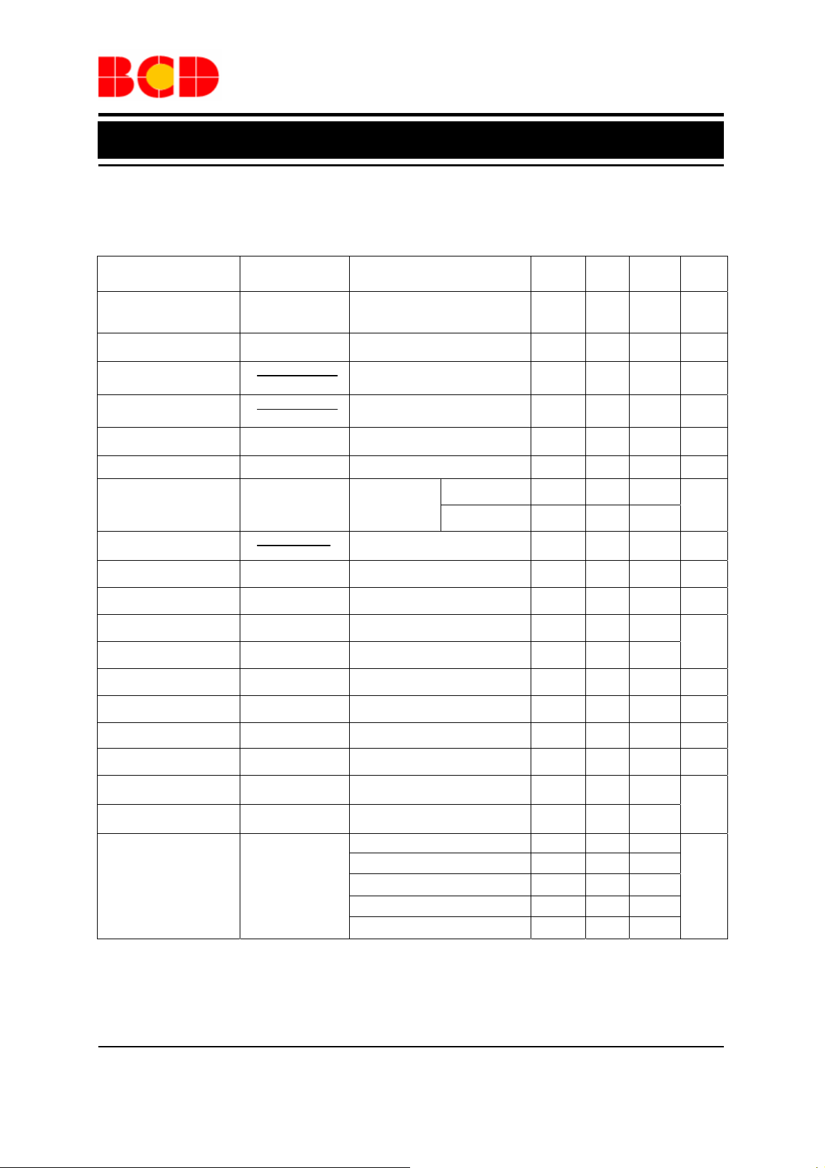
AP2114-1.8 Electrical Characteristics (Note 2)
(VIN=2.8V, CIN=4.7μF (Ceramic), C
ranges, unless otherwise specified (Note 3))
Parameter Symbol Test Conditions Min Typ Max Unit
=4.7μF (Ceramic), Typical T
OUT
= 25°C, Bold typeface applies over -40
A
O
C≤TA≤85OC
Output Voltage V
Maximum Output Current I
Load Regulation
Line Regulation
△V
△V
Dropout Voltage V
Quiescent Current IQ V
Power Supply Rejection
Ratio
Output Voltage
△V
Temperature Coefficient
Short Current Limit I
RMS Output Noise V
V
OUT
VIN=2.8V, V
OUT(MAX)
OUT/VOUT
I△
OUT
OUT/VOUT
V△
IN
I
DROP
=2.8V, 1mA ≤ I
IN
=2.8V, 1mA ≤ I
V
IN
2.8V≤VIN≤6V, I
=1.0A 500 700 mV
OUT
=2.8V, I
IN
Ripple 1Vp-p
PSRR
OUT/VOUT
T△
V
SHORT
10Hz ≤ f ≤100kHz (No load) 30
NOISE
=2.8V,
V
IN
I
=100mA
OUT
I
=30mA, TA =-40°C to 85°C
OUT
=0V 50 mA
OUT
V
≤ 30mA
OUT
=1.773V to 1.827V 1.0 A
OUT
≤1A 0.2 1.0 %/A
OUT
=30mA -0.1 0.02 0.1 %/V
OUT
=0mA 60 75
OUT
OUT
×98.5%
f=100Hz 68
f=1KHz 68
±30
1.8
V
OUT
×101.5%
ppm/°C
VEN High Voltage VIH Enable logic high, regulator on 1.5
VEN Low Voltage VIL Enable logic low, regulator off 0.4
Standby Current I
V
STD
=2.8V, VEN in OFF mode 0.01 1.0
IN
μV
V
μA
dB
RMS
V
μA
Start-up Time t
EN Pull Down Resistor
V
Discharge Resistor
OUT
Thermal Shutdown
Temperature
Thermal Shutdown
Hysteresis
R
T
T
HYOTSD
S
R
3.0
PD
Set EN pin at Low 60
DCHG
160
OTSD
o Load 20
μs
MΩ
Ω
°C
25
SOIC-8 74.6
PSOP-8 43.7
Thermal Resistance
(Junction to Case)
θ
JC
SOT-223 50.9
°C /W
TO-252-2 (1) /(3) /(4) 35
TO-263-3 22
Note 2: To prevent the Short Circuit Current protection feature from being prematurely activated, the input
voltage must be applied before a current source load is applied.
Note 3: Production testing at T
Jan. 2013 Rev. 2. 2 BCD Semiconductor Manufacturing Limited
=25°C. Over temperature specifications guaranteed by design only.
A
10
N
Data Sheet
1A LOW NOISE CMOS LDO REGULATOR WITH ENABLE AP2114
Electrical Characteristics (Continued)
AP2114-2.5 Electrical Characteristics (Note 2)
(VIN=3.5V, C
ranges, unless otherwise specified (Note 3))
Parameter Symbol Test Conditions Min Typ Max Unit
=4.7μF (Ceramic), C
IN
=4.7μF (Ceramic), Typical T
OUT
= 25°C, Bold typeface applies over -40
A
O
C≤TA≤85OC
Output Voltage V
Maximum Output Current I
Load Regulation
Line Regulation
△V
△V
Dropout Voltage V
Quiescent Current IQ V
Power Supply Rejection
Ratio
Output Voltage
△V
Temperature Coefficient
Short Current Limit I
RMS Output Noise V
V
OUT
OUT(MAX)
VIN=3.5V, V
OUT/VOUT
I△
OUT
OUT/VOUT
V△
IN
I
DROP
=3.5V, 1mA ≤ I
IN
Vout=2.5V, V
1mA ≤ I
OUT
3.5V≤VIN≤6V, I
=1A 450 750 mV
OUT
=3.5V, I
IN
Ripple 1Vp-p
PSRR
OUT/VOUT
T△
V
SHORT
10Hz ≤ f ≤100kHz 30
NOISE
=3.5V,
V
IN
=100mA
I
OUT
I
=30mA
OUT
=0V 50 mA
OUT
V
≤ 30mA
OUT
=2.463V to 2.537V 1.0 A
OUT
=Vout+1V
IN
≤1A
=30mA -0.1 0.02 0.1 %/V
OUT
=0mA 60 80
OUT
OUT
×98.5%
0.2 1.0 %/A
f=100Hz 65
f=1KHz 65
±30
2.5
V
OUT
×101.5%
ppm/°C
VEN High Voltage VIH Enable logic high, regulator on 1.5
VEN Low Voltage VIL Enable logic low, regulator off 0.4
Standby Current I
V
STD
=3.5V, VEN in OFF mode 0.01 1.0
IN
μV
V
μA
dB
RMS
V
μA
Start-up Time tS
EN Pull Down Resistor RPD 3.0
V
Discharge Resistor R
OUT
Thermal Shutdown
Temperature
Thermal Shutdown
Hysteresis
Set EN pin at Low 60
DCHG
160
T
OTSD
25
T
HYOTSD
o Load 20
μs
MΩ
Ω
°C
SOIC-8 74.6
PSOP-8 43.7
Thermal Resistance
(Junction to Case)
θ
JC
SOT-223 50.9
°C /W
TO-252-2 (1) /(3) /(4) 35
TO-263-3 22
Note 2: To prevent the Short Circuit Current protection feature from being prematurely activated, the input
voltage must be applied before a current source load is applied.
Note 3: Production testing at T
=25°C. Over temperature specifications guaranteed by design only.
A
Jan. 2013 Rev. 2. 2 BCD Semiconductor Manufacturing Limited
11
 Loading...