

Page 1

Service Manual
LT2619SU/LT2621SU
Page 2

LCD TV Service Manual
Contents
Contents................................................................................................................................................................- 2 -
Service Manual ....................................................................................................................................................- 3 -
1. Precautions and notices..............................................................................................................................- 3 -
1.1 WARNING ......................................................................................................................................- 4 -
1.2 NOTES ............................................................................................................................................- 7 -
2. Product Function Specifications..............................................................................................................- 10 -
2.1 Product Function............................................................................................................................- 10 -
2.2 Specifications.................................................................................................................................- 12 -
3. LCD Panel Spec.......................................................................................................................................- 13 -
3.1 General Description.......................................................................................................................- 13 -
3.2 General Features............................................................................................................................- 13 -
4. Chassis Layout and Overall Wiring Diagrams........................................................................................- 14 -
4.1 Chassis Layout...............................................................................................................................- 14 -
4.2 Wires and Cables Overall Wiring Diagrams .................................................................................- 15 -
5. Factory/Service OSD Menu and Adjustment...........................................................................................- 16 -
5.1 T o enter the Factory OSD Menu....................................................................................................- 16 -
5.2 Factory OSD Menu........................................................................................................................- 16 -
6. Software Upgrading.................................................................................................................................- 20 -
6.1 Get ready for upgrading.................................................................................................................- 20 -
6.2 Upgrading with the ISP_TOOL4.0.9.............................................................................................- 29 -
7. Troubleshooting.......................................................................................................................................- 34 -
7.1 Troubleshooting for Remote Control.............................................................................................- 34 -
7.2 Troubleshooting for Function Key.................................................................................................- 35 -
7.3 TV won’t Power On.......................................................................................................................- 36 -
7.4 Troubleshooting for Audio.............................................................................................................- 37 -
7.5 Troubleshooting for TV/VGA/HDMI input...................................................................................- 38 -
7.6 Troubleshooting for YPbPr input...................................................................................................- 39 -
7.7 Troubleshooting for Video/S-Video/ SCART input.......................................................................- 40 -
8. Explode View...........................................................................................................................................- 41 -
9. Schematic circuit diagram.......................................................................................................................- 41 -
- 2 -
Page 3

LCD TV Service Manual
Service Manual
1. Precautions and notices
BEFORE SERVICING THE LCD TV, READ THE SAFETY PRECAUTIONS IN
THIS MANUAL.
WHEN REPLACEMENT PARTS ARE REQUIRED, BE SURE TO USE
REPLACEMENT PARTS SPECIFIED BY THE MANUFACTURER.
- 3 -
Page 4

LCD TV Service Manual
not undertaken any such broad evaluation. Accordingly, a serviceman that uses a
service procedure or tools, which are not recommended by Hisense, must first satisfy
himself thoroughly that neither his safety nor the safe of the equipment will be
jeopardized by the service method selected.
1.1 WARNING
1.1.1
DANGERCAUTION CAUTION
TO ENSURE THE CONTINUED RELIABILITY OF THIS PRODUCT, USE ONLY
ORIGINAL MANUFACTURER'S REPLACEMENT PARTS, WHICH ARE LISTED WITH
THEIR PART NUMBERS IN THE PARTS LIST SECTION OF THIS SERVICE GUIDE.
- 4 -
Page 5

1.1.2.
All ICs and many other semiconductors are susceptible to electrostatic discharges
(ESD). Careless handling during repair can reduce life drastically. When repairing,
make sure that you are connected with the same potential as the mass of the set by a
wristband with resistance. Keep components and tools also at this same potential.
1. Never replace modules or other components while the unit is switched on.
2. When making settings, use plastic rather than metal tools. This will prevent
any short circuits and the danger of a circuit becoming unstable.
1.1.3
LCD TV Service Manual
To prevent electrical shock, do not use this polarized ac plug with an extension cord,
receptacle, or the outlet unless the blades can be fully inserted to prevent blade
exposure.
To prevent electrical shock, match wide blade or plug to wide slot, fully insert.
1.1.4
When replacement parts are required, be sure to use replacement parts specified by
the manufacturer or have the same characteristics as the original part. Unauthorized
substitutions may result in fire, electric shock, or other hazards.
1.1.5
Safety regulations require that after a repair the set must be returned in its original
condition. In particular attention should be paid to the following points.
-Note: The wire trees should be routed correctly and fixed with the mounted
- 5 -
Page 6

cable clamps.
-The insulation of the mains lead should be checked for external damage.
1.1.6
(1) Do not touch Signal and Power Connector while this product operates. Do not
touch EMI ground part and Heat Sink of Film Filter.
(2) Do not supply a voltage higher than that specified to this product. This may
damage the product and may cause a fire.
(3) Do not use this product in locations where the humidity is extremely high,
where it may be splashed with water, or where flammable materials surround it. Do
LCD TV Service Manual
not install or use the product in a location that does no satisfy the specified
environmental conditions. This may damage the product and may cause a fire.
(4) If a foreign substance (such as water, metal, or liquid) gets inside the panel
module, immediately turn off the power. Continuing to use the product may cause
fire or electric shock.
(5) If the product emits smoke, and abnormal smell, or makes an abnormal sound,
immediately turn off the power. Continuing to use the product, it may cause fire or
electric shock.
(6) Do not disconnect or connect the connector while power to the product is on. It
takes some time for the voltage to drop to a sufficiently low level after the power
has been turned off. Confirm that the voltage has dropped to a safe level before
disconnecting or connecting the connector.
- 6 -
Page 7

(7) Do not pull out or insert the power cable from/to an outlet with wet hands. It
may cause electric shock.
(8) Do not damage or modify the power cable. It may cause fire or electric shock.
(9) If the power cable is damaged, or if the connector is loose, do not use the
product: otherwise, this can lead to fire or electric shock.
(10) If the power connector or the connector of the power cable becomes dirty or
dusty, wipe it with a dry cloth. Otherwise, this can lead to fire.
(11) Use only with the cart, stand, tripod, bracket, or table specified by the
manufacturer, or sold with the apparatus. When a cart is used, use caution when
LCD TV Service Manual
moving the cart/apparatus combination to avoid injury from tip-over.
1.2 NOTES
Notes on Safe Handling of the LCD panel and during service
The work procedures shown with the Note indication are important for ensuring the
safety of the product and the servicing work. Be sure to follow these instructions.
• Before starting the work, secure a sufficient working space.
• At all times other than when adjusting and checking the product, be sure to turn
OFF the POWER Button and disconnect the power cable from the power source of
the TV during servicing.
• To prevent electric shock and breakage of PC board, start the servicing work at least
30 seconds after the main power has been turned off. Especially when installing and
removing the power board, start servicing at least 2 minutes after the main power has
- 7 -
Page 8

been turned off.
• While the main power is on, do not touch any parts or circuits other than the ones
specified. If any connection other than the one specified is made between the
measuring equipment and the high voltage power supply block, it can result in
electric shock or activation of the leakage-detection circuit breaker.
• When installing the LCD module in, and removing it from the packing carton, be
sure to have at least two persons perform the work.
• When the surface of the panel comes into contact with the cushioning materials, be
sure to confirm that there is no foreign matter on top of the cushioning materials
LCD TV Service Manual
before the surface of the panel comes into contact with the cushioning materials.
Failure to observe this precaution may result in, the surface of the panel being
scratched by foreign matter.
• When handling the circuit board, be sure to remove static electricity from your body
before handling the circuit board.
• Be sure to handle the circuit board by holding the large parts as the heat sink or
transformer. Failure to observe this precaution may result in the occurrence of an
abnormality in the soldered areas.
• Do not stack the circuit boards. Failure to observe this precaution may result in
problems resulting from scratches on the parts, the deformation of parts, and
short-circuits due to residual electric charge.
• Routing of the wires and fixing them in position must be done in accordance with
- 8 -
Page 9

the original routing and fixing configuration when servicing is completed. All the
wires are routed far away from the areas that become hot (such as the heat sink).
These wires are fixed in position with the wire clamps so that the wires do not move,
thereby ensuring that they are not damaged and their materials do not deteriorate over
long periods of time. Therefore, route the cables and fix the cables to the original
position and states using the wire clamps.
• Perform a safety check when servicing is completed. Verify that the peripherals of
the serviced points have not undergone any deterioration during servicing. Also
verify that the screws, parts and cables removed for servicing purposes have all been
LCD TV Service Manual
returned to their proper locations in accordance with the original setup.
The lightning flash with arrowhead symbol, within an equilateral
triangle is intended to alert the user to the presence of uninsulated
dangerous voltage within the products enclosure that may be of sufficient magnitude
to constitute a risk of electric shock.
The exclamation point within an equilateral triangle is intended to
alert the user to the presence of important operating and maintenance
(servicing) instructions in the literature accompanying the set.
- 9 -
Page 10
2. Product Function Specifications
2.1 Product Function
LCD TV Service Manual
- 10 -
Page 11
LCD TV Service Manual
- 11 -
Page 12
2.2 Specifications
LCD TV Service Manual
- 12 -
Page 13
LCD TV Service Manual
3. LCD Panel Spec
3.1 General Description
V260B1- L02 is a 25.5” TFT Liquid Crystal Display module with 8-CCFL
Backlight unit and RSDS interface.
This module supports 1366 x 768 WXGA format and can display 16.2M colors
(6-bits+FRC colors).
3.2 General Features
Item Specification Unit
Active Area
Bezel Opening Area 580.8 (H) x 328.8 (V) mm
Driver Element a-si TFT active matrix
Pixel Number 1366 x R.G.B. x 768 pixel
Pixel Pitch (Sub Pixel) 0.1405 (H) x 0.4215 (V) mm
Pixel Arrangement RGB vertical stripe Display Colors 16.2M color
Display Operation
Mode
Surface Treatment Anti-Glare coating (Haze 25%) Hard coating (3H) -
575.769 (H) x 323.712
(V)
Transmissive mode / Normally White -
(26” diagonal) mm
- 13 -
Page 14
(2)
(6)
(4)
(3)
LCD TV Service Manual
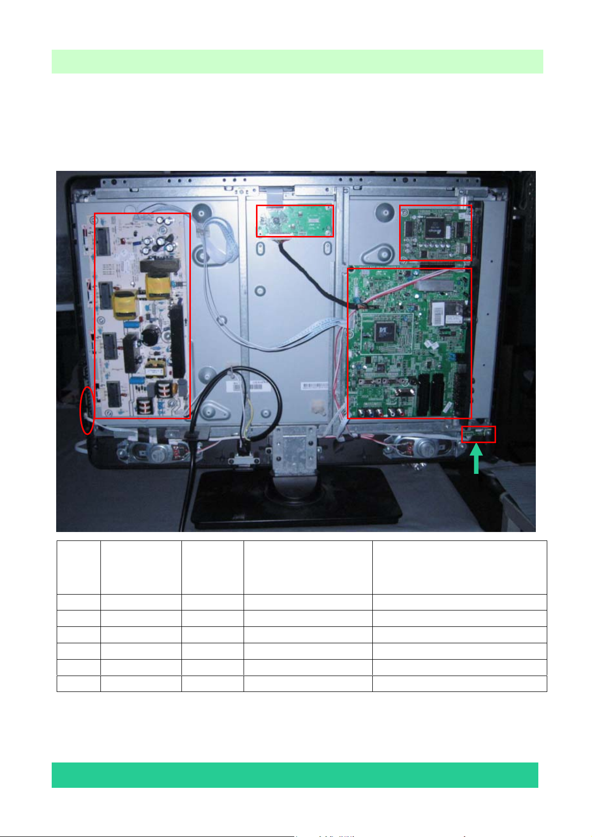
4. Chassis Layout and Overall Wiring Diagrams
4.1 Chassis Layout
(1)
(5)
No Description Part No
(1)
(2)
(3)
(4)
(5)
(6)
Main Board 117379 RSAG2.908.1395-1\ROH RSAG7.820.1529\VERCROH
Power Board 115429 RSAG2.908.1251\ROH RSAG7.820.1235\VER.C\ROH
RUSB Board
TCON Board
Keypad PCA
IR&Led Board 116295
114583
115643
117301
Type/Model PCB/ Model
RSAG2.908.1189\ROH
RSAG2.908.1268TP\ROH RSAG7.820.1330\VERC\ROH
RSAG2.908.1088-1\ROH
RSAG2.908.1260-2\ROH
RSAG7.820.1272\VER.B\ROH
RSAG7.820.1101\VER.B\ROH
RSAG7.820.1337\VER.B\ROH
- 14 -
Page 15
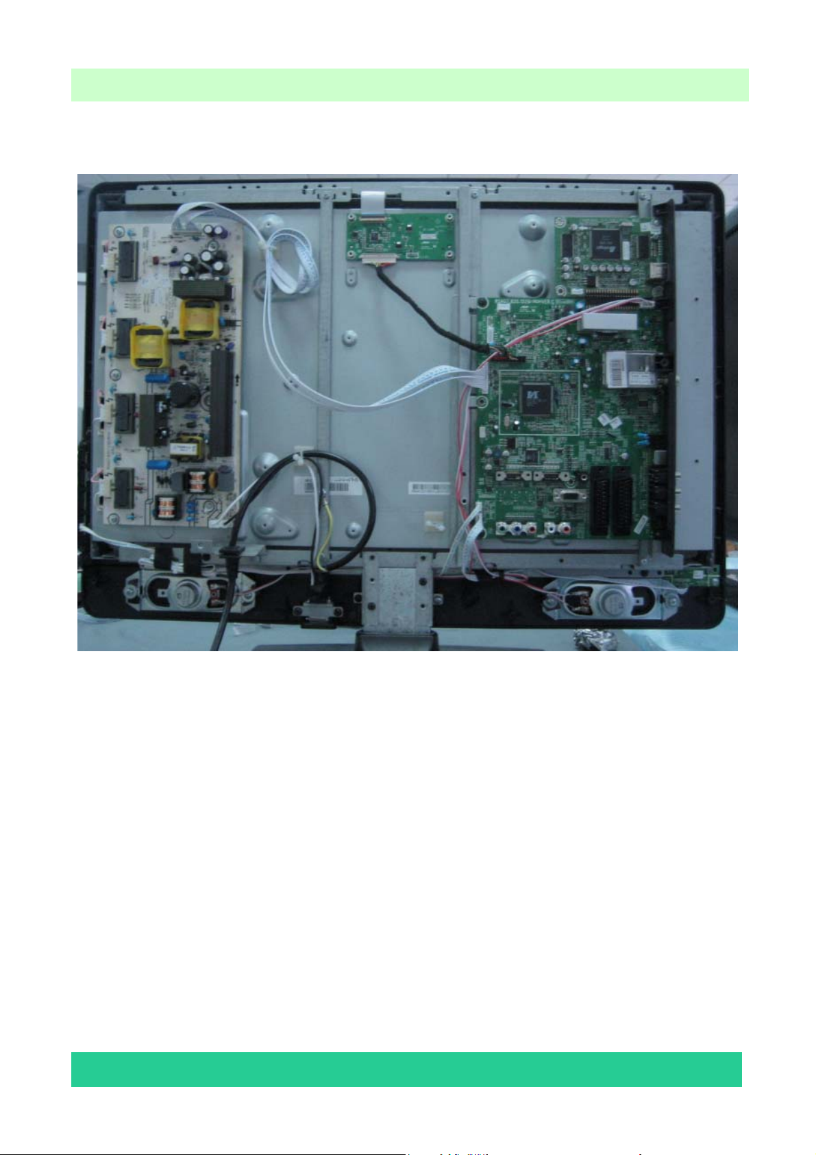
LCD TV Service Manual
4.2 Wires and Cables Overall Wiring Diagrams
- 15 -
Page 16

LCD TV Service Manual
5. Factory/Service OSD Menu and Adjustment
5.1 To enter the Factory OSD Menu
a. With factory RC (remote control)
1. Press “M” button and enter factory mode.
2. Press “Menu” button and enter factory OSD menu.
3 . Press “CH+”/“CH-” button select the function menu, press “VOL+”/“VOL-” enter the
selected function menu. Press “VOL+”/“VOL-” button adjust values in the menu.
4. Press “M” button exit factory mode in the factory OSD menu.
When TV outgoing factory,user can not enter factory OSD menu with Factory Remote
b. With user’s RC
1. Power TV On
2. Press Menu button and call up User OSD Menu
3. Select Sound-> Balance
4. When Balance value is “0”,Enter 0->5->3 ->2 in sequence.
Note: If necessary, re-do number keys.
5. Factory OSD appears.
6. Press the standby button then AC turn off and restart the TV, which can exit factory OSD
menu.
5.2 Factory OSD Menu
The Factory OSD Menu comprises Factory Menu and Design Menu .
5.2.1、Factory Menu
Factory Menu
White Balance
Auto Test
Auto Calibration
LOGO
OSD Language
Country
Option
Factory Init
Test Pattern
Version:
White Balance
R DRV 8
G DRV 10
B DRV 10
R CUT 136
G CUT 130
B CUT 121
BRIGHT_H 80
CONTRAST _H 80
BRIGHT_L 40
CONTRAST_L 40
- 16 -
Page 17

LCD TV Service Manual
Auto Calibration
Auto Color
Color Temp. Standard
RED COLOR 136
GREEN COLOR 130
BLUE COLOR 121
Option
SOURCE TV
BRIGHT 0 10
BRIGHT 50 100
BRIGHT 100 150
CONTRAST 0 60
CONTRAST 50 100
CONTRAST 100 150
TOFAC M
HDMI Cable Standard
DQS PHASE 3
LOGO
NULL
HISENSE
WELCOME
EGYPT OFF
Factory Init
QingDao
HuangDao
Guiyang
shunde
Hungary
France
Australia
CLEAR PROTECTLY
CLEAR UNPROTECTLY
Turkey
- 17 -
Page 18

LCD TV Service Manual
Test Pattern
BLUE
5.2.2、Design Menu
Design Menu
Picture Mode
Sound Mode
Sound Settings
Power Save
PIP Option
EMI
MOVESHARPNESS
LipSync
Version
Version:
Panel Type:
V260B1- L02 (1366*768)
FLASH :
- 18 -
Page 19

LCD TV Service Manual
Picture Mode
Standard Brightness 50
Contrast 50
Colour 50
Bright Brightness 60
Contrast 60
Colour 55
Soft Brightness 45
Contrast 45
Colour 45
Sound Settings
VOLUME 0 128
VOLUME 1 79
VOLUME 20 27
VOLUME 40 23
VOLUME 100 8
TVPRE SCALER 6
VOLUME SCALER 0
Sound Mode
Standard 120Hz 12
500Hz 10
1.5KHz 11
5KHz 8
10KHz 15
Music 120Hz 19
500Hz 11
1.5KHz 12
5KHz 14
10KHz 20
Speech 120Hz 4
500Hz 10
1.5KHz 12
5KHz 7
10KHz 5
- 19 -
Page 20

LCD TV Service Manual
6. Software Upgrading
The software is upgraded by a burning tool- ISP_TOOL4.0.9, which can burn the
program file“*.bin” to the main board of the unit
6.1 Get ready for upgrading
6.1.1 Install the ISP_TOOL4.0.9-------only for the first time update.
1、 Port Setting:
Choose “system”option from the “control panel”
- 20 -
Page 21

Click the “system” icon as the following
Choose the “hardware” option from the dialog window
LCD TV Service Manual
- 21 -
Page 22

Click“device management” icon as the following
Choose the port (COM and LPT1)
LCD TV Service Manual
Choose the ECP print port (LPT1)
- 22 -
Page 23

Click the port of print (LPT1)as the following
LCD TV Service Manual
Choose “port setting”option as the following
- 23 -
Page 24

Find the folder where the ISP_TOOL4.0.9 lies in.
2、
There are three folders/files in this folder together.
DLPORTIO.dll and FTD2XX.DLL must be in the same folder
LCD TV Service Manual
Double click the ISP_TOOL4.0.9 icon, and then a dialog window will show as below.
- 24 -
Page 25

Click the Config button. And then a dialog window will show as below.
Port Type setting is LPT1
Base Addr setting is 0x378
Draw on the front of “pin 1 switch UART/I2c”
Speed setting is 99
As following
LCD TV Service Manual
Choose“SDA in”and setting “PIN” is “PIN10”。
Notes:
Do not draw on the front of “Reverse High”。
As following
- 25 -
Page 26

Choose “SCL in”and setting “PIN” is “PIN11”。
Notes:
Do not draw
As following
Choose “SDA out”and setting “PIN” is “PIN4”
Notes:
Draw on the front of “Reverse High”。
As following。
on the front of “Reverse High”。
LCD TV Service Manual
Choose “SCL out”and setting “PIN” is “PIN2”
Notes:
Draw
As following
on the front of “Reverse High”
- 26 -
Page 27

After having finished all above, clicking the “Apply ”button to complete the configuration。
LCD TV Service Manual
6.1.2 Hardware connecting
You can update the software through a special tool (as following)
- 27 -
Page 28

Connect the Debug board to the TV use VGA interface, the other parallel port to the
computer, just as the following。
LCD TV Service Manual
- 28 -
Page 29

LCD TV Service Manual
6.2 Upgrading with the ISP_TOOL4.0.9
6.2.1 Double click the ISP_TOOL4.0.9 icon and a dialog window will show as following。
Click the“Read ”button。
- 29 -
Page 30

Choose the update file from the folder。
LCD TV Service Manual
- 30 -
Page 31

The update file has been chosen successfully。
Click the“Auto”button and choose parameters as following。
Click the“Run”button
LCD TV Service Manual
Click the“connect”button,then show a dialog box as following。
- 31 -
Page 32

If show above then click the“Run”button again and again,till show the following dialog
window。
LCD TV Service Manual
- 32 -
Page 33

LCD TV Service Manual
The above appears on the screen-the word “program ok”shows in the information
displaying window,indicating upgrading is ov er。
6.2.2 After the update is over. Must Confirm the software Version in the Version Menu.
If the update is successful, enter Factory Init Menu and select “Clear Unprotectly”
a. Press VOL+ button to clear the EEPROM data.
b. When the “Clear Unprotectly ” button becomes white, turn off the power.
c. Restart the TV.
- 33 -
Page 34

LCD TV Service Manual
7. Troubleshooting
7.1 Troubleshooting for Remote Control
Remote control does not work
YES
Try new batteries
Replace battery
NO
Replace RC
YES
Replace remote control
NO
Check IR receiver
Change Led & IR board
NO
Change Led & IR cable
YES
Replace Led & IR BD
YES
Replace Led & IR cable
NO
Replace main board
- 34 -
Page 35

LCD TV Service Manual
7.2 Troubleshooting for Function Key
Buttons does not work
Check switches
YES
Replace tact switch
NO
Check key board
YES
Replace Key BD
NO
Check Key BD cable
Change Key BD cable
YES
OK
NO
Replace main board
- 35 -
Page 36

7.3 TV won’t Power On
LCD TV Service Manual
TV won’t power on
Is LED light?
NO
Check Power
Inlet
YES
Make Sure Power
source is live
YES
NO
BLUE
RED
OSD?
NO
YES
Check signal
Source
YES
NO
Check Power
Cord
NO
Try Power on by
RC and Button
Neither
works
Replace Main
BD
YES
Only
one works
Both
Work
Replace
Power Cord
Check/replace IR
BD or Keypad
PCA
NO
Replace Panel
Replace Main BD
OK
YES
Power on
NO
Replace Power BD
YES
OK
- 36 -
Page 37

LCD TV Service Manual
7.4 Troubleshooting for Audio
No sound
Check connecter
YES
Reconnect
NO
Check speaker wire
NO
Check speaker set
YES
YES
Replace speaker wire
Replace speaker set
NO
Replace main board
YES
OK
- 37 -
Page 38

LCD TV Service Manual
7.5 Troubleshooting for TV/VGA/HDMI input
No picture on the screen
NO
Check Signal Source
Make sure signal
source is available
YES
Check connect
Reconnect
NO
Check cable
YES
Replace cable
NO
Replace main board
- 38 -
Page 39

LCD TV Service Manual
7.6 Troubleshooting for YPbPr input
No picture on the screen
Check Source work or not
YES
Check connect
NO
Check Wires (Green Blue, Red)
NO
Replace main board
NO
YES
YES
Check Source Device
Reconnect
Replace wires
- 39 -
Page 40

LCD TV Service Manual
7.7 Troubleshooting for Video/S-Video/ SCART input
No picture on the screen
Check Source work or not
YES
NO
Check Signal Source
YES
Check connect
Reconnect
NO
Check Cable/ Wires
YES
Replace Cable/Wires
NO
Check SCART BD
YES
Replace SCART BD
NO
Replace main board
- 40 -
Page 41

8. Explode View
9. Schematic circuit diagram
LCD TV Service Manual
- 41 -
Page 42

Page 43

BBK LT2619SU PARTS LIST
No. Part No. Description Qty. Code Number Remark
118625 Front Cover 1 RSAG8.074.552\Z4\ROH
1
1052188 Bracket 1 RSAG8.078.481\B2\Z3\ROH
2
1044829 Button Bracket 1 RSAG8.335.067\Z0\ROH
3
117301 Keypad PCA 1 RSAG2.908.1088-1\ROH
4
1046628 Speaker 2 YDT4211E-5W8R-F\ROH
5
1036391 Block 1 RSAG8.634.047\black\ROH
6
1050066 Bracket 2 RSAG8.038.1303\ROH
7
118870 LCD Panel 1 V260B1-L02\HS\BL\ROH
8
115429 Power Board 1 RSAG2.908.1251\ROH
9
1050067 Bracket 1 RSAG8.038.1304\ROH
10
1046924 Power Cord 1 YS-1\ROH
11
1049574 Stand 1 RSAG6.121.053\ROH
12
1050055 Rear Cover 1 RSAG8.074.541\Z0\ROH
13
1052003 Side Label 1 RSAG8.804.3280\ROH
14
1053175 Bottom Label 1 RSAG8.804.3317 \ROH
15
1055349 Rating Label 1 RSAG8.807.3922
16
1048779 Bracket Unit 2 RSAG6.150.452\ROH
17
117379 Main Board 1 RSAG2.908.1395-1\ROH
18
1053183 Terminal Bracket 1 RSAG8.081.447\Z0\ROH
19
1050068 Bracket Unit 1 RSAG4.114.052\ROH
20
Please
order
them
together
Page 44

Page 45

BBK LT2621SU PARTS LIST
No. Part No. Description Qty. Code Number Remark
118626 Front Cover 1 RSAG8.074.556\Z3\ROH
1
1052188 Bracket 1 RSAG8.078.481\B2\Z3\ROH
2
1044829 Button Bracket 1 RSAG8.335.067\Z0\ROH
3
117301 Keypad PCA 1 RSAG2.908.1088-1\ROH
4
1046628 Speaker 2 YDT4211E-5W8R-F\ROH
5
1036391 Block 1 RSAG8.634.047\black\ROH
6
1050066 Bracket 2 RSAG8.038.1303\ROH
7
118870 LCD Panel 1 V260B1-L02\HS\BL\ROH
8
115429 Power Board 1 RSAG2.908.1251\ROH
9
1050067 Bracket 1 RSAG8.038.1304\ROH
10
1046924 Power Cord 1 YS-1\ROH
11
1049574 Stand 1 RSAG6.121.053\ROH
12
1050055 Rear Cover 1 RSAG8.074.541\Z0\ROH
13
1052003 Side Label 1 RSAG8.804.3280\ROH
14
1053175 Bottom Label 1 RSAG8.804.3317 \ROH
15
1055349 Rating Label 1 RSAG8.807.3922
16
1048779 Bracket Unit 2 RSAG6.150.452\ROH
17
18
19
20
117379 Main Board 1 RSAG2.908.1395-1\ROH
1053183 Terminal Bracket 1 RSAG8.081.447\Z0\ROH
1050068 Bracket Unit 1 RSAG4.114.052\ROH
Please
order them
together
Page 46

5
4
3
2
1
+12V_all
D D
CA1
CA1
16V 470uF
1
2
3
4
5
6
7
8
9
10
11
12
13
14
BL-ON/OFF
IPWM|GND
STANDBY
+5V_all
+12V_all
16V 470uF
C2
0.1uFC20.1uF
L31 BLM31PG121SN1L31 BLM31PG121SN1
L33 BLM31PG121SN1L33 BLM31PG121SN1
R3100R310
0
BL-ADJ
40V
5Vstb5Vstb
XP9XP9
V1
3904V13904
5Vstb
R1
4.7KR14.7K
R2NCR2
NC
R4
POWER-ON/OFFPOWER-ON/OFF
4.7KR44.7K
1
2 3
ON-PBACK
ADJ-PWM3
POWER-ON/OFF
ON-PBACK
ADJ-PWM3
R15 NCR15 NC
R16
R16
4.7K
4.7K
R21
R21
4.7K
4.7K
5Vstb
R13
R13
R121KR12
10K
10K
1K
BL-ON/OFF
V4
1
3904V43904
R181KR18
1K
2 3
1
2 3
V6
3904V63904
BL-ADJ
C10
C10
2.2uF
2.2uF
R115
R115
10K
10K
+5V_all
R304
R304
4.7K
4.7K
R303NCR303
NC
IPWM|GND
CN3
CN3
1
2
C C
B B
3
4
CON4_2.0
CON4_2.0
Vcc_A
1
2
3
4
Vcc_A
A A
Title
Title
Title
<Title>
<Title>
<Title>
Size Document Number Rev
Size Document Number Rev
Size Document Number Rev
MST9E19A 2.0
A3
MST9E19A 2.0
A3
MST9E19A 2.0
A3
of
Date: Sheet of
Date: Sheet of
5
4
3
2
Date: Sheet
119Saturday, July 12, 2008
119Saturday, July 12, 2008
119Saturday, July 12, 2008
1
Page 47

5
A
D D
R379 47KR379 47K
R394
R394
12K
12K
R390 47KR390 47K
R397
R397
12K
12K
R386 47KR386 47K
DMP-Lin
DMP-Rin
12
14
15
11
1
5
2
4
10
9
R385 47KR385 47K
R391 47KR391 47K
R384 47KR384 47K
PC-Lin
SC2_Lin
DMP-Lin
PC-Rin
SC2_Rin
DMP-Rin
A-SW02
A-SW12
C394 2.2uFC394 2.2uF
C353 2.2uFC353 2.2uF
C381 2.2uFC381 2.2uF
C393 2.2uFC393 2.2uF
C383 2.2uFC383 2.2uF
C400 2.2uFC400 2.2uF
A-SW0
A-SW1
R378
R378
10K
10K
+5VA
INPAQ_VPORT
INPAQ_VPORT
INPAQ_VPORT
INPAQ_VPORT
R381
R381
10K
10K
1 2
D116
D116
1 2
R382 100R382 100
R395 100R395 100
R396
R396
10K
10K
R399
R399
10K
10K
D123
D123
C216
C216
560pF
560pF
C217
C217
560pF
560pF
PC-Lin
SC2_Lin
DMP-Lin
PC-Rin
SC2_Rin
DMP-Rin
C C
DMP-L
B B
DMP-R
U29
U29
X0
X1
X2
X3
Y0
Y1
Y2
Y3
A
B
74HC4052
74HC4052
R408
R408
R40347KR40347K
R405
R405
R404
R404
R407
R407
R406 47KR406 47K
R387
R387
10K
10K
VCC
GND
INH
VEE
47K
47K
47K
47K
4
47K
47K
47K
47K
R383 10KR383 10K
CA23
CA23
100uF/16V
100uF/16V
13
X
3
Y
16
8
6
7
+5VA
C321
C321
0.1uF
0.1uF
C355
C355
10uF
10uF
+5VA
MUX-Lin
MUX-Rin
ON_USB1,2
MUX-Lin 2
MUX-Rin 2
ON_USB
DMP-VOUT
IO1
IO1
528 amend
R130 10KR130 10K
5Vstb
R40 4.7KR40 4.7K
3
DMP-VOUT
C392 100PC392 100P
R5360R536
1
C105
C105
0.1uF
0.1uF
D2
SMB5818D2SMB5818
2
XS11
XS11
2
USB3_5V
4
GND
6
USB2_5V
8
GND
10
USB1_5V
12
R36975R369
75
14
16
18
20
22
24
26
28
30
32
34
36
38
40
C192
C192
330pF
330pF
GND
MR_OUT
Y_OUT
PR_OUT
COM_PR
CVBS_IN
GND
TXD
REMOTE
GPIO1
SCL1
NC
VCC5V
GND
MR_IN
R36875R368
75
POWER_USB
C210
C210
330pF
330pF
DMP-R
R520 0R520 0
TXD
0
DMP-Y DMP-Yin
DMP-PB
DMP-PR
D102
D102
1 2
INPAQ_VPORT
INPAQ_VPORT
DMP-R
DMP-Y DMP-PB
DMP-PR
IR-in
D110
D110
D101
D101
C208
C208
330pF
1 2
INPAQ_VPORT
INPAQ_VPORT
INPAQ_VPORT
INPAQ_VPORT
330pF
1 2
1
DM3
3
DP3
5
DM2
7
DP2
9
DM1
11
DP1
13
ML_OUT
15
PB_OUT
17
GND
19
COM_PB
21
COM_Y
23
GND
25
RXD
27
29
GPIO2
31
SDA1
33
ID
35
VCC5V
37
GND
39
ML_IN
40P-2X20
40P-2X20
CA28 10uFCA28 10uF
CA29 10uFCA29 10uF
CA30 10uFCA30 10uF
R28675R286
75
MAX:3A
R72
R72
100/NC
100/NC
1
Q7
2 3
3904Q73904
C369
C369
47uF
47uF
U11
U11
MP1583
MP1583
1
BS
2
IN
3
SW
4
GND
VCC_USB5V
C391
C391
100P
100P
C389
C389
1.5nF
1.5nF
MP1583
MP1583
SYN
COMP
GND
9
L15
L15
+5V_all
BLM31PG121SN1
BLM31PG121SN1
R451
R451
33K
33K
+12V_all
+12V_all
R352
R352
200K
C390
C390
100P
100P
R445
R445
4.7K
4.7K
200K
R440
R440
100K
100K
8
7
EN
6
5
FB
R447
R447
10K
10K
R51 4.7KR51 4.7K
2 3
L77
L77
4.7uH
4.7uH
Q6
3904Q63904
C397
C397
100P
100P
C396
C396
16V 470uF
16V 470uF
VCC_USB5V
DMP-PBin
DMP-PRin
DMP-L
ON_USBIR-in
1
DMP-Yin
DMP-PBin
DMP-PRin
DMP-L
ON_USB
RXD
R5260 R5260
A
Title
Title
Title
<Title>
<Title>
<Title>
Size Document Number Rev
Size Document Number Rev
Size Document Number Rev
<Doc> <RevCod
A3
<Doc> <RevCod
A3
<Doc> <RevCod
A3
of
Date: Sheet of
Date: Sheet of
Date: Sheet
11Wednesday, July 16, 2008
11Wednesday, July 16, 2008
11Wednesday, July 16, 2008
Page 48

5
[ASIC Control]
D D
VDD33
R172NCR172
NC
TEST
R178NCR178
NC
R3NCR3
NC
BIST
SC0
[Terminator near T-CON]
RXE0-/G3
RXE1-/G1
BISTBIST CLKNCLKN
RXE2-/B7
RXEC-/B5
RXE3-/B3
N3
IRF7314N3IRF7314
1
S1
2
C294
C294
100n
100n
VOUT
VOUT
GND
1
G1
3
S2
4
G2
~420mA
CA53
CA53
+
+
100uF/16V
100uF/16V
2
4
CA54
CA54
+
+
100uF/16V
100uF/16V
R328
R328
10K
10K
2 3
2
4
N36
N36
AIC1117-18
AIC1117-18
3
VIN
V52
V52
3904
3904
+12V_all
PANEL-ON/OFF
L35 FBL35 FB
LVDS-SL/SCL
+5V_all
LVDS-SL/SCL
C C
PANEL-ON/OFF
B B
VCC-Panel
A A
L36
L36
NC/600(4.5X3.2)
NC/600(4.5X3.2)
L37
L37
R27 4.7KR27 4.7K
V5V
100uF/16V
100uF/16V
R333 100R333 100
600(4.5X3.2)
600(4.5X3.2)
1
CA57
CA57
C272
C272
+
+
R330
R330
0.1UF
0.1UF
R28
R28
10K
10K
2 3
2.2R
2.2R
CA55
CA55
100uF/16V
100uF/16V
R336
R336
100
100
R367 4.7KR367 4.7K
V8
3904V83904
N34
N34
254-33
254-33
3
VOUT
VIN
VOUT
GND
1
R-SOT4N-2.30-7.00-HX
R-SOT4N-2.30-7.00-HX
C276
C276
+
+
0.1UF
0.1UF
1
MST7381B Cancel
4
VDD33
R5
R311
R311
10K
10K
4.7KR54.7K
SC1
R14 100R14 100
R327 100R327 100
R335 100R335 100
R334 100R334 100
R329 100R329 100
8
7
6
5
C275
C275
0.1UF
0.1UF
RXE0+/G2
RXE1+/G0RXE1-/G1
RXE2+/B6
VCC-Panel
VDD33
RXE0-/G3
RXE2-/B7
RXEC-/B5 RXEC+/B4
RXE3-/B3 RXE3+/B2
D1
D1
D2
D2
~250mA
C277
C277
0.1UF
0.1UF
VDD_1.8
MST7381B Cancel
用于
MST7381B与MST7382B
MST7381B C3=1uF
MST7382B C3=0.1uF
RXE0+/G2
RXE1+/G0
RXE2+/B6
RXEC+/B4
RXE3+/B2
兼容
VDD_1.8
R212
R212
10K
10K
C3
1uF/0.1uFC31uF/0.1uF
RXE0-/G3
RXE0-/G3
RXE0+/G2
RXE0+/G2
RXE1-/G1
RXE1-/G1
RXE1+/G0
RXE1+/G0
RXE2-/B7
RXE2-/B7
RXE2+/B6
RXE2+/B6
RXEC-/B5
RXEC-/B5
RXEC+/B4
RXEC+/B4
RXE3-/B3
RXE3-/B3
RXE3+/B2
RXE3+/B2
MST7381B Cancel
MST7381B 19pin为NC
3
VDD33
R211 10KR211 10K
VDDC_T
SC0
SC1
VDD_1.8
1
2
3
4
5
6
7
8
9
10
11
12
13
14
15
16
SC0
SC1
GPO1
GPO2
VCC_LVDS
RO0N
RO0P
RO1N
RO1P
RO2N
RO2P
ROCKN
ROCKP
RO3N
RO3P
GND_LVDS
RESETRESETRESET
C1
1uFC11uF
VDDC_T
RESET
63
GPO064GPO3
1IN/1OUT RSDS
1IN/1OUT RSDS
GND17VDDP218DVDD19REL20GND_RSDS21B2P22B2N23B1P24B1N25B0P26B0N27VCC_RSDS28G2P29G2N30G1P31G1N
POL_SI
TCON_SDA
TCON_SCL
TEST
PDI
59
62
58
56
61
57
60
PDI
SCL
SDA
TEST
VDDC
GNDC
RESET
U2
U2
MST7381B / MST7382B
MST7381B / MST7382B
54
55
VDDP
POL_SI
TESTPAD1TESTPAD1
BIST
53
49
51
52
50
OE
STV
STH
CPV
BIST
POL
TP1
VCC_RSDS
R0N
R0P
GND_RSDS
R1N
R1P
R2N
R2P
CLKN
CLKP
VCC_RSDS
GND_RSDS
G0N
G0P
32
1
48
47
46
45
44
43
42
41
40
39
38
37
36
35
34
33
VDD33
TESTPAD2TESTPAD2
1
POL_SI PDIBIST
2
TESTPAD3TESTPAD3
1
R6 22R6 22
R7 22R7 22
R8 22R8 22
R9 22R9 22
R11 22R11 22
B2P
B2N
B1P
B1N
B0P
B0N
CLKPCLKP
G2P
G2N
G1P
G1N
G0P
G0NG0N
R2PR2P
R2NR2N
R1PR1P
R1NR1N
R0PR0P
R0NR0N
R323 22R323 22
R325 22R325 22
GVOFF
CKVCKVCKVCKVCKVCKV
STV
STH
1
47
46
OE
B2P
R10
R10
10K
10K
POL
TP
VDD33V5V
V5V
B2N
B1P
B1N
B0P
B0N
G2P
G2N
G1P
G1N
G0P
G0N
CLKP
CLKN
R2P
R2N
R1P
R1N
R0P
R0N
STH
TP
POL
STV
CKV
OE
GVOFFGVOFF
45
44
43
42
41
40
39
38
37
36
35
34
33
32
31
30
29
28
27
26
CON1
CON1
25
24
45PIN
45PIN
23
22
21
20
19
18
17
16
15
14
13
12
11
10
9
8
7
6
5
4
3
2
1
Debug port
TCON_SCL
TCON_SDA
V5V
CA56
CA56
+
+
2200uF/16V
2200uF/16V
C4
NC/0.1uFC4NC/0.1uF
C5
NC/1000pFC5NC/1000pF
R337
R337
100
100
[I2C EEPROM for LUT]
R339 4K7R339 4K7
U3
1
3
4
A0
A12WP
A2
GND
24C64U324C64
VCC
SCL
SDA
8
7
6
5
R338 4K7R338 4K7
TCON_SCL
TCON_SDA
VDD33
R340NCR340
NC
R3501KR350
1K
C215
C215
0.1uF
0.1uF
XP7
XP7
CON5_2.0
CON5_2.0
V5V
1
2
3
4
5
[Filter near T-CON]
VDD33
C221
0.1uF
0.1uF
C220
C220
0.1uF
0.1uF
C221
0.1uF
0.1uF
C33
C33
C222
C222
0.1uF
0.1uF
C223
C223
0.1uF
0.1uF
C224
C224
0.1uF
0.1uF
Title
Title
Title
Mstar_738xB for T-con
Mstar_738xB for T-con
Mstar_738xB for T-con
Size Document Number Rev
Size Document Number Rev
Size Document Number Rev
of
Date: Sheet of
Date: Sheet of
5
4
3
2
Date: Sheet
11Saturday, July 12, 2008
11Saturday, July 12, 2008
11Saturday, July 12, 2008
1
Page 49

5
4
N5
Vcc3.3for MST9E19A analog
5Vstb
L6
L6
BLM31PG121SN1
BLM31PG121SN1
D D
+3.3AVDD for
AVDD_HDMI
+3.3Vstb AVDD_HDMI
L8 BLM18PG181SN1L8 BLM18PG181SN1
C17
C17
2.2uF
2.2uF
+3.3AVDD for
AVDDA
C C
+3.3Vstb AVDDA
L10
L10
BLM18PG181SN1
BLM18PG181SN1
3.3V for
AVDDPLL2
+3.3Vstb AVDD_MemPLL
L12
L12
BLM18PG181SN1
BLM18PG181SN1
C23
C23
2.2uF
2.2uF
C27
C27
2.2uF
2.2uF
C18
C18
0.1uF
0.1uF
pin36
C24
C24
0.1uF
0.1uF
C28
C28
0.1uF
0.1uF
pin6,pin12
N5
AMS1117-3.3
AMS1117-3.3
ADJ
OUT
ADJ
OUT
IN
IN
3
2
1
C11
C11
0.1uF
0.1uF
C19
C19
0.1uF
0.1uF
+3.3AVDD
for AVDD_SIF
+
CA6
+
CA6
47uF/16V
47uF/16V
+3.3AVDD for
AVDD_AU
C12
C12
0.1uF
0.1uF
+3.3Vstb
L9 BLM18PG181SN1L9 BLM18PG181SN1
+3.3Vstb AVDD_SIF
+3.3V for
VDD_MPLL
+3.3Vstb
L13 BLM18PG181SN1L13 BLM18PG181SN1
+3.3Vstb
+
+
AVDD_AU
L11 BLM18PG181SN1L11 BLM18PG181SN1
VDD_MPLL
CA7
CA7
47uF/16V
47uF/16V
C20
C20
2.2uF
2.2uF
1 2
C29
C29
2.2uF
2.2uF
C25
C25
2.2uF
2.2uF
4
C21
C21
0.1uF
0.1uF
C30
C30
0.1uF
0.1uF
C26
C26
0.1uF
0.1uF
C22
C22
2.2uF
2.2uF
C31
C31
0.1uF
0.1uF
3
0.81*(1+Rup/Rdown)=1.8V---Rup=10K, Rdown=8.2K
5Vstb
CA10
CA10
+
+
47uF
47uF
FB
L38FBL38
Vcc1.2 for MST9E19B
R25 10KR25 10K
U6
AOZ1041U6AOZ1041
1
PGND
2
VIN
AGND3EN
4
FB
C14
C14
0.1uF
0.1uF
C96
C96
0.1uF
0.1uF
LX2
LX1
COMP
L7
3.3uHL73.3uH
R23 3KR23 3K
C95
C95
0.1uF
0.1uF
EMC201
EMC201
1
2
3
4
5
6
CON6
CON6
1
2
3
4
5
6
0.1uF
0.1uF
C13
C13
12
R24
R24
3.9K
3.9K
C32
C32
0.1uF
0.1uF
R263KR26
3K
8
7
6
5
R83
R83
3.9K
3.9K
+
+
CA9
CA9
47uF
47uF
C16
C16
0.1uF
0.1uF
VDDC
C15
C15
0.1uF
0.1uF
2
1
Vcc3.3for MST9E19A
+
CA12
+
CA12
47uF/16V
47uF/16V
Digital
C34
C34
0.1uF
0.1uF
5
C35
C35
0.1uF
0.1uF
C36
C36
0.1uF
0.1uF
C37
C37
0.1uF
0.1uF
C38
C38
0.1uF
0.1uF
C39
C39
0.1uF
0.1uF
C40
C40
0.1uF
0.1uF
C41
C41
0.1uF
0.1uF
C42
C42
0.1uF
0.1uF
4
+3.3Vstb VDDP VDDC
L14 BLM31PG121SN1L14 BLM31PG121SN1
B B
A A
VDDC for MST9E19A Core
C45
C45
C46
C46
C47
C43
C43
0.1uF
0.1uF
C44
C44
0.1uF
0.1uF
0.1uF
0.1uF
0.1uF
0.1uF
C47
0.1uF
0.1uF
C48
C48
0.1uF
0.1uF
C49
C49
0.1uF
0.1uF
深圳市高新区南区科技南十路国际技术创新研究院C座4楼
深圳市高新区南区科技南十路国际技术创新研究院C座4楼
深圳市高新区南区科技南十路国际技术创新研究院C座4楼
TEL:0755-26996895 FAX:0755-26996830
TEL:0755-26996895 FAX:0755-26996830
TEL:0755-26996895 FAX:0755-26996830
Title
Title
Title
Title
Title
Title
<Title>
<Title>
<Title>
Size Document Number Rev
Size Document Number Rev
Size Document Number Rev
Size Document Number Rev
Size Document Number Rev
Size Document Number Rev
A3
A3
A3
<Doc> 2.0
A3
<Doc> 2.0
A3
<Doc> 2.0
A3
Date: Sheet
Date: Sheet
Date: Sheet of
Date: Sheet of
Date: Sheet of
3
2
Date: Sheet of
power
power
power
MST9E19A
MST9E19A
MST9E19A
Saturday, July 12, 2008
Saturday, July 12, 2008
Saturday, July 12, 2008
219Saturday, July 12, 2008
219Saturday, July 12, 2008
219Saturday, July 12, 2008
of
1
of
Page 50

5
D D
R_TX2+
R_TX2+
R_TX2-
R_TX2-
G_TX1+
G_TX1+
G_TX1-
G_TX1-
B_TX0+
B_TX0+
B_TX0-
B_TX0TXCLK+
TXCLK-
HDMI_SDA
HDMI_SCL
HS_RGB
VS_RGB
DMP-SOG
HDTV_SOG
SCR+
SCG+
SCB+
SC_FSW
SC_FS
SCART2_Cin+
SCART2_Vin+
S1-Cin
S1-Yin
S1-YinAV1-Vin+
AV2/SC1-Vin+
TV1-Vin+
TV1-Vin-
TXCLK+
TXCLK-
HDMI_SDA
HDMI_SCL
HS_RGB
VS_RGB
BIN+
BIN+
BIN-
BIN-
DMP-SOG
GIN+
GIN+
GIN-
GIN-
RIN+
RIN+
RIN-
RIN-
HDTV_SOG
SCR+
SCR-
SCR-
SCG+
SCG-
SCG-
SCB+
SCB-
SCB-
SC_FSW
SC_FS
SCART2_Cin+
SCART2_Vin+
S1-Cin
S1-Yin
S1-Yin-
AV1-Vin+
AV2/SC1-Vin+
TV1-Vin+
TV1-Vin-
TV-SIFP SIFP
TV-SIFP
TV-SIFM SIFM
TV-SIFM
C91
C91
CA15
CA15
0.1uF
0.1uF
10uF/16V
10uF/16V
L34
L34
BLM18PG181SN1
BLM18PG181SN1
HDMI
INPUT
VGA/DMP
INPUT
C C
SCART/YPBPR
INPUT
VIDEO
INPUT
B B
CA16
CA16
10uF/16V
10uF/16V
Debug port
A A
XP3
XP3
CON4_2.0
CON4_2.0
5
R29
R29
10K
10K
R65 47R65 47
R66 47R66 47
AUVREF
AUVRADP
C90
C90
0.1uF
0.1uF
AUVRADN
1
1
2
2
3
3
4
4
C62
C62
0.1uF
0.1uF
5Vstb
VDDP
3
1
R50
R50
390R1%
390R1%
C64 10nFC64 10nF
C65 10nFC65 10nF
C69 10nFC69 10nF
C70 10nFC70 10nF
C71 10nFC71 10nF
C72 10nFC72 10nF
C73 10nFC73 10nF
C74 10nFC74 10nF
C75 10nFC75 10nF
C76 10nFC76 10nF
C77 10nFC77 10nF
C78 0.1uFC78 0.1uF
C79 0.1uFC79 0.1uF
HD_Lin
HD_Rin
AV1-Lin
AV1-Rin
MUX-Lin
MUX-Rin
AV2/SC1-Lin
AV2/SC1-Rin
TXD
RXD
RXD
TXD
2
D9
BAV99D9BAV99
R361KR36
1K
CA14
CA14
10uF/16V
10uF/16V
AVDD_HDMI
C61
C61
0.1uF
0.1uF
C59
C59
0.1uF
0.1uF
C60
C60
0.1uF
0.1uF
TXD
RXD
1
C63
C63
0.1uF
0.1uF
SV_C1
SV_Y1
SV_C0
SV_Y0
VCOM2
CVBS3
CVBS2
CVBS1
VCOM1
TUNER_CVBS
VCOM0
HD_PC-Lin
HD_PC-Rin
AV1-Lin
AV1-Rin
R67 0R67 0
AV2/SC1-Lin
AV2/SC1-Rin
R78 10R78 10
R79 10R79 10
CVBSOut
I2C-SDA
I2C-SCL
V7
3906V73906
3 2
R39
R39
10K
10K
TUNER_CVBS
C80 2.2uFC80 2.2uF
C81 2.2uFC81 2.2uF
C82 2.2uFC82 2.2uF
C83 2.2uFC83 2.2uF
C84 2.2uFC84 2.2uF
C85 2.2uFC85 2.2uF
C86 2.2uFC86 2.2uF
C87 2.2uFC87 2.2uF
C88 2.2uFC88 2.2uF
CA13
CA13
47uF/16V
47uF/16V
SYS_RST
R37 1KR37 1K
C53
C53
22pF
22pF
C58
C58
22pF
22pF
TXCLK-
1
TXCLK+
2
B_TX0-
4
B_TX0+
5
G_TX1-
7
G_TX1+
8
R_TX2-
10
R_TX2+
11
13
HDMI_SDA
14
HDMI_SCL
15
HS_RGB
16
VS_RGB
17
18
19
20
21
BIN+
22
BIN-
23
DMP-SOG
24
GIN+
25
GIN-
26
RIN+
27
RIN-
28
SCB-
29
SCB+
30
SCG-
31
SCG+
32
HDTV_SOG
33
SCR-
34
SCR+
35
SC_FS
38
SC_FSW
39
SV_C1
40
SV_Y1
41
SV_C0
42
SV_Y0
43
VCOM2
44
CVBS3
45
CVBS2
46
CVBS1
47
VCOM1
48
49
VCOM0
50
CVBSOut
51
SIFP
54
SIFM
55
AUVRADN
57
AUVRADP
58
AUVREF
59
61
62
63
64
AUCOM
65
66
67
68
69
AUOutL3
70
AUOutR3
71
AUOutL2
72
AUOutR2
73
AMP-Lout
74
AMP-Rout
75
76
78
79
80
81
82
83
84
85
86
87
5Vstb
R77
R77
R76
R76
4.7K
4.7K
4.7K
4.7K
DDC-TXD
DDC-RDX
KEY0
KEY1
SC2_FS
Mode Selection
ADJ-PWM3
PWM2
PWM1/WP_FSH
PWM0
1 2
Z2
14.318MHZZ214.318MHZ
RXCKN
RXCKP
RX0N
RX0P
RX1N
RX1P
RX2N
RX2P
REXT
DDCD_DA
DDCD_CK
HSYNC1
VSYNC1
RMID
VCLAMP
REFP
REFM
BIN1P
BIN1M
SOGIN1
GIN1P
GIN1M
RIN1P
RIN1M
BIN0M
BIN0P
GIN0M
GIN0P
SOGIN0
RIN0M
RIN0P
HSYNC0
VSYNC0
C1
Y1
C0
Y0
VCOM2
CVBS3
CVBS2
CVBS1
VCOM1
CVBS0
VCOM0
CVBSOUT
SIF1P
SIF1M
AUVRADN
AUVRADP
AUVREF
AUL0
AUR0
AUL1
AUR1
AUCOM
AUL2
AUR2
AUL3
AUR3
AUOUTL3
AUOUTR3
AUOUTL2
AUOUTR2
AUOUTL
AUOUTR
AUOUTS
VDI2/GPIOF2
VDI3/GPIOF3
VDI4/GPIOF4
VDI5/GPIOF5
VDI6/GPIOF6
VDI7/GPIOF7
VDI8/GPIOF8
VDI9/GPIOF9
VDICLK/GPIOF10
GPIOF11
131
4
D100
D100
C54
C54
1nF
1nF
1 2
INPAQ_VPORT
INPAQ_VPORT
129
R85NCR85
NC
R891KR89
1K
205
HWRESET
PWM0
PWM1
130
4
PWM2
PWM3
155
156
AVDD_SIF
AVDDA
36
AVDD_ADC
IRIN
136
IR_SYNC
D120
D120
INPAQ_VPORT
INPAQ_VPORT
1 2
ADJ-PWM3
PWM2
PWM1/WP_FSH
PWM0
VDDP
R871KR87
R86NCR86
1K
NC
R91NCR91
R901KR90
NC
1K
R451MR45
1M
206
207
XIN
XOUT
GPIOF_SEL=01,VDO_PORT_SEL=00 for I2S input
DDCR_DA
DDCR_CK
DDCA_DA
DDCA_CK
SAR0
SAR1
SAR2
SAR3
132
133
134
125
126
127
128
R841KR84
1K
R88NCR88
NC
AVDD_AU
53
AVDD_SIF
AVDD_MemPLL
60
AVDD_AU
ADJ-PWM3
VDD_MPLL
AVDD_HDMI
105
12
AVDD_DVI6AVDD_DVI
AVDD_MEMPLL
N8
MST9E19AN8MST9E19A
GND3GND9GND37GND52GND56GND89GND99GND
157
208
AVDD_MPLL
AVDD_MPLL
101
104
GND
VDDC
GND
106
VDDC77VDDC98VDDC
GND
GND
120
141
3
Location Near IC Pin.
R30
R30
AMP-Rout
100
AMP-Lout
100
R42
R42
100
100
VDDP
RP10
RP8
RP8
RP4.7KX4
RP4.7KX4
R46
R46
SCL_EXT
100
SDA_EXT
102
103
VDDP
VDDP
100
R49
R49
100
100
119
140
151
159
172
186
VDDP
VDDP
VDDP
VDDP
VDDP
VDDP
SCL_EXT
SDA_EXT
VDDP
100
107
142
158
203
VDDP88VDDP
VDDC
VDDC
VDDC
RP10
4321
4321
4321
4321
RP4.7KX4
RP4.7KX4
5678
5678
5678
5678
113
112
111
110
109
108
AD4
AD3
AD2
AD1
AD0
AU_SWAP=11
HDCEC
HD-VSW0
AMP-MUTE
Overdrive
LED_RED
115
114
AD7
AD6
AD5
AISD/DI7
AISCK/DI6
AIWS/DI5
IVSYNC
IHSYNC
HDCEC
HD-VSW0
AMP-MUTE
202
201
200
199
DI4
198
DI3
197
DI2
196
DI1
195
DI0
ICLK
SPDIF_OUT
192
194
193
更改部分
GPIOE2/LDE
GPIOE3/LCK
PWM_SENSE
VDDP
4321
4321
5678
5678
LB0M/R7
LB0P/R6
LB1M/R5
LB1P/R4
LB2M/R3
LB2P/R2
LBCKM/R1
LBCKP/R0
LB3M/G7
LB3P/G6
LB4M/G5
LB4P/G4
LA0M/G3
LA0P/G2
LA1M/G1
LA1P/G0
LA2M/B7
LA2P/B6
LACKM/B5
LACKP/B4
LA3M/B3
LA3P/B2
LA4M/B1
LA4P/B0
GPIOF19
GPIOF18
GPIOF17
GPIOF16
GPIOF15
GPIOF14
GPIOF13
GPIOF12
PWM_DRV
PWM_FB
RP5
RP5
RP4.7KX4
RP4.7KX4
SDO
CSZ
SDI
SCK
5Vstb
191
190
189
188
RXE0-/R7
185
RXE0+/R6
184
RXE1-/R5
183
RXE1+/R4
182
RXE2-/R3
181
RXE2+/R2
180
RXEC-/R1
179
RXEC+/R0
178
RXE3-/G7
177
RXE3+/G6
176
RXE4-/G5
175
RXE4+/G4
174
RXE0-/G3
171
RXE0+/G2
170
RXE1-/G1
169
RXE1+/G0
168
RXE2-/B7
167
RXE2+/B6
166
RXEC-/B5
165
RXEC+/B4
164
RXE3-/B3
163
RXE3+/B2
162
RXE4-/B1
161
RXE4+/B0
160
SPI_DO
124
SPI_CZ
123
SPI_DI
122
SPI_CK
121
97
96
95
94
R151 33KR151 33K
93
R153 33KR153 33K
92
R154 33KR154 33K
91
R187 33KR187 33K
90
LG NEW CHANGE PVR IO
139
138
137
R81
R81
4.7K
4.7K
A-SW1
HD-VSW1
A-SW0
HDMI_WP
POWER-ON/OFF
ON-PBACK
HPDCTRL
HDMI_SEL1
PANEL-ON/OFF
USB-PW
HDMI_SEL2
KEY0
KEY1
LVDS-SL/SCL
BRI_OUT
RXE0-/G3
RXE0+/G2
RXE1-/G1
RXE1+/G0
RXE2-/B7
RXE2+/B6
RXEC-/B5
RXEC+/B4
RXE3-/B3
RXE3+/B2
VDDP
RP14
RP14
4321
4321
5678
5678
RP4.7KX4
RP4.7KX4
IO4
IO4
IO3
IO3
IO2
IO2
IO1IO1IO1
IO1
V10
V10
NC/3904
NC/3904
IR_SYNC
R60 0R60 0
2 3
R63
R63
NC/4.7K
NC/4.7K
V9
R56 NC/1KR56 NC/1K
1
NC/3904V9NC/3904
2 3
R58 1KR58 1K
C67
C67
100pF
100pF
NC/4.7K
NC/4.7K
R59 1KR59 1K
R64NCR64
R57
R57
C68
C68
NC
100pF
100pF
R62NCR62
NC
GPIOE0/LVSYNC
GPIOE1/LHSYNC
GND
GND
GND
GND
DIGO0
DIGO1
DIGO2
DIGO3
DIGO4
DIGO5
DIGO6
DIGO7
DIGO8
DIGO9
WRZ
RDZ
ALE
152
173
187
204
143
144
145
146
147
148
WP
149
150
153
154
116
117
A-SW1
A-SW0
HDMI_WP
POWER-ON/OFF
ON-PBACK
HPDCTRL
INT
118
135
R197
R197
R182
R182
R180
R180
R3004.7K R3004.7K
R4574.7K R4574.7K
3
R416
R416
4.7K
4.7K
4.7K
4.7K
4.7K
4.7K
4.7K
4.7K
PANEL-ON/OFF
C51
C51
10nF
10nF
C56
C56
10nF
10nF
更改部分
1
+3.3Vstb
R52
R52
2.2K
2.2K
2
AMP-R
AMP-R
R35
R35
22K
22K
AMP-L
AMP-L
R47
R47
22K
22K
VCC-Panel
14
RXE0+/R6
RXE1+/R4
RXE2+/R2
RXEC+/R0
RXE3+/G6
RXE4+/G4
28
RXE0+/G2
RXE1+/G0
RXE2+/B6
RXEC+/B4
RXE3+/B2
38
RXE4+/B0
40
WP:Mstar PULL DOWN
PWM1/WP_FSH
5Vstb
R53
R53
4.7K
4.7K
R61
R61
IR-inIR-in_USB
100
100
IR-in
C66
C66
100pF
100pF
R54
R54
2.2K
2.2K
KEY0-in
KEY1-in
KEY1-in
2
Location Near IC Pin.
R31
R31
AUOutR3
100
100
R44
R44
AUOutL3
100
100
LED_RED
R157 470R157 470
CON8
CON8
2
VCC
4
VCC
6
GND
8
GND
LVDS_SL/SCL10AI/SDA
BRI_OUT12BRI_EXT/DIS
GND
TXA0+16TXA0TXA1+18TXA1TXA2+20TXA2TXAC+22TXACTXA3+24TXA3TXA4+26TXA4GND
TXB0+30TXB0TXB1+32TXB1TXB2+34TXB2TXBC+36TXBCTXB3+
TXB4+
VCC
VCC
GND
GND
GND
GND
TXB3TXB4-
40P-2X20
40P-2X20
R69 33KR69 33K
R70NCR70
NC
I2C address
at A0.
HDCP I2C address
at A4.
AUOut3-R
R33
R33
C52
C52
22K
22K
1nF
1nF
AUOut3-L
C57
C57
1nF
1nF
R48
R48
22K
22K
5Vstb
V43
V43
1
1
3
5
7
9
11
13
RXE0-/R7
15
RXE1-/R5
17
RXE2-/R3
19
RXEC-/R1
21
RXE3-/G7
23
RXE4-/G5
25
27
RXE0-/G3
29
RXE1-/G1
31
RXE2-/B7
33
RXEC-/B5
35
RXE3-/B3
37
RXE4-/B1
39
BRI_OUT LVDS-SL/SCL
VDDP
R68
R68
4.7k
4.7k
C199
C199
0.1uF
0.1uF
N10
N10
24C32
24C32
1
A0
VCC
2
A1
WP
3
A2
SCL
GND4SDA
R80 10KR80 10K
N11
N11
24C04
24C04
1
A0
VCC
2
A1
WP
3
A2
SCL
GND4SDA
1
Location Near IC Pin.
R32
R32
AUOut3-R
R195
R195
1K0
1K0
3904
3904
2 3
R782 NCR782 NC
L29 BLM18PG181SN1L29 BLM18PG181SN1
1
2
3
8
7
6
5
8
7
6
5
AUOutR2
AUOutL2
AUOut3-L
KEY1-in
KEY1-in
KEY0-in
D117
D117
D118
D118
LED-R
INPAQ_VPORT
INPAQ_VPORT
1 2
1 2
INPAQ_VPORT
INPAQ_VPORT
+3.3Vstb
VCC-Panel
R287NCR287
NC
R270
R270
27K
27K
R288
R288
10K
10K
N9
PS25VF040N9PS25VF040
8
CE#
VDD
SO
HOLD#
WP#
SCK
VSS4SI
5Vstb
R71
R71
10K
10K
WP
5Vstb
WP_EP
Title
Title
Title
MST9E19A
MST9E19A
MST9E19A
Size Document Number Rev
Size Document Number Rev
Size Document Number Rev
MST9E19A 2.0
A2
MST9E19A 2.0
A2
MST9E19A 2.0
A2
Date: Sheet
Date: Sheet
Date: Sheet
C89
C89
0.1uF
0.1uF
7
6
5
R295
R295
R159
R159
4.7K
4.7K
4.7K
4.7K
SCL
SDA
Debug port
XP4
XP4
C93
C93
0.1uF
0.1uF
SCL
CON5_2.0
CON5_2.0
SDA
深圳市高新区南区科技南十路国际技术创新研究院C座4楼
深圳市高新区南区科技南十路国际技术创新研究院C座4楼
深圳市高新区南区科技南十路国际技术创新研究院C座4楼
TEL:0755-26996895 FAX:0755-26996830
TEL:0755-26996895 FAX:0755-26996830
TEL:0755-26996895 FAX:0755-26996830
1
AUOut2-R
100
100
C50
C50
R34
R34
10nF
10nF
22K
22K
R38
R38
100
100
INPAQ_VPORT
INPAQ_VPORT
AUOut2-L
R43
R43
C55
C55
22K
22K
10nF
10nF
XP2
XP2
1
2
3
CON3_2.0
CON3_2.0
IR-in
LED-R
5Vstb
D119
D119
1 2
LVDS-SL/SCL
Location Near IC
C203
C203
2.2uF
2.2uF
RP3
RP3
C198
C198
RP33X4
RP33X4
NC/10pF
NC/10pF
4321
4321
C92
C92
0.1uF
0.1uF
R74
R74
I2C-SCL
100
100
I2C-SDA
R75
R75
100
100
5Vstb
R73
R73
10K
10K
SDA
1
SCL
2
WP_EPWP_EP
3
4
5
R82NCR82
NC
319Saturday, July 12, 2008
319Saturday, July 12, 2008
319Saturday, July 12, 2008
CON5_2.0
CON5_2.0
5678
5678
of
of
of
AUOut2-R
AUOut2-L
XP1
XP1
1
2
3
4
5
SPI_CK
SPI_DI
SPI_CZ
SPI_DO
Page 51

1
2
3
4
5
6
7
8
9
10
11
12
13
14
15
16
17
18
19
D21
D21
INPAQ_VPORT
INPAQ_VPORT
1
2
3
4
5
6
7
8
9
10
11
12
13
14
15
16
17
18
19
INPAQ_VPORT
INPAQ_VPORT
1 2
D34
D34
1 2
D22
D22
INPAQ_VPORT
INPAQ_VPORT
INPAQ_VPORT
INPAQ_VPORT
HDMI2/5V
HDMI2-HPD
HDMI2-DDC-SCL
HDMI2-DDC-SDA
HDMI1/5V
D23
D23
1 2
INPAQ_VPORT
INPAQ_VPORT
HDMI1/5V
HDMI1-HPD
HDMI1-DDC-SCL
HDMI1-DDC-SDA
HDMI2/5V
D35
D35
1 2
INPAQ_VPORT
INPAQ_VPORT
HDMI1-RX2+
HDMI1-RX2HDMI1-RX1+
HDMI1-RX1HDMI1-RX0+
HDMI1-RX0HDMI1-RXC+
HDMI1-RXC-
R1001KR100
1K
D24
D24
1 2
HDMI2-RX2+
HDMI2-RX2HDMI2-RX1+
HDMI2-RX1HDMI2-RX0+
HDMI2-RX0HDMI2-RXC+
HDMI2-RXC-
R2031KR203
1K
HDMI2-HPD
HDMI2-DDC-SCL
HDMI2-DDC-SDA
D36
D36
1 2
INPAQ_VPORT
INPAQ_VPORT
HDMI1-HPD
HDMI1-DDC-SCL
HDMI1-DDC-SDA
D26
D26
1 2
INPAQ_VPORT
INPAQ_VPORT
INPAQ_VPORT
INPAQ_VPORT
D37
D37
1 2
INPAQ_VPORT
INPAQ_VPORT
CEC
5Vstb
D18
D18
1
BAT54C
BAT54C
5Vstb
1 2
D27
D27
1 2
CEC
D38
D38
2
1 2
INPAQ_VPORT
INPAQ_VPORT
1
2
D39
D39
1 2
INPAQ_VPORT
INPAQ_VPORT
3
R101
R101
10K
10K
R3641KR364
D28
D28
D29
D29
1K
1 2
D30
D30
BAT54C
BAT54C
3
R332
R332
10K
10K
R10911KR1091
D40
D40
1K
1 2
R103
R103
R102
R102
4K7
4K7
10K
10K
R104
R104
100
100
R105
R105
100
100
R2511KR251
V11
V11
1K
1
3904
3904
2 3
R341
R341
R343
R343
4K7
4K7
10K
10K
R363
R363
100
100
R158
R158
100
100
R2541KR254
V12
V12
1K
1
3904
3904
2 3
P1
DATA2+
DATA2 SHIELD
DATA2-
20
DATA1+
GND1
DATA1 SHIELD
21
DAT1A-
GND2
DATA0+
22
DATA0 SHIELD
GND3
DATA0-
23
CLK+
GND4
CLK SHIELD
24
CLK-
GND5
CEC
NC
SCL
SDA
DDC/CEC GND
+5V POWER
HOT PLUG
HDMI_JP1HDMI_J
D D
HDMI1-RX1HDMI1-RX1+
HDMI1-RX2HDMI1-RX2+
HDMI1-RXCHDMI1-RXC+
HDMI1-RX0HDMI1-RX0+
1 2
INPAQ_VPORT
INPAQ_VPORT
INPAQ_VPORT
INPAQ_VPORT
D412
D412
1 2
DIODE EGA-0603
DIODE EGA-0603
D410
D410
1 2
DIODE EGA-0603
DIODE EGA-0603
D411
D411
1 2
DIODE EGA-0603
DIODE EGA-0603
D409
D409
1 2
DIODE EGA-0603
DIODE EGA-0603
P2
DATA2+
DATA2 SHIELD
DATA2-
20
DATA1+
GND1
DATA1 SHIELD
21
DAT1A-
GND2
DATA0+
22
DATA0 SHIELD
GND3
C C
DATA0-
23
CLK+
GND4
CLK SHIELD
24
CLK-
GND5
CEC
NC
SCL
SDA
DDC/CEC GND
+5V POWER
HOT PLUG
HDMI_JP2HDMI_J
HDMI2-RX1HDMI2-RX1+
HDMI2-RX2HDMI2-RX2+
HDMI2-RXCHDMI2-RXC+
HDMI2-RX0HDMI2-RX0+
D33
D33
1 2
INPAQ_VPORT
INPAQ_VPORT
INPAQ_VPORT
INPAQ_VPORT
D405
D405
1 2
DIODE EGA-0603
DIODE EGA-0603
D406
D406
1 2
DIODE EGA-0603
DIODE EGA-0603
D407
D407
1 2
DIODE EGA-0603
DIODE EGA-0603
D408
D408
B B
1 2
DIODE EGA-0603
DIODE EGA-0603
5
R92 10R92 10
R93 10R93 10
R94 10R94 10
R95 10R95 10
R96 10R96 10
R97 10R97 10
R98 10R98 10
R99 10R99 10
R106 NCR106 NC
R133 NCR133 NC
R342 10R342 10
R346 10R346 10
R351 10R351 10
R331 10R331 10
R345 10R345 10
R317 10R317 10
R299 10R299 10
R348 10R348 10
8
7
6
5
R349 NCR349 NC
R347 NCR347 NC
8
7
6
5
HPDCTRL
N19
N19
24C02
24C02
HPDCTRL
N12
N12
24C02
24C02
VCC
WP
SCL
VCC
WP
SCL
HDMI_WP
HDMI1_SCL
HDMI1_SDA
RX2_2+
RX2_2RX2_1+
RX2_1RX2_0+
RX2_0RX2_C+
RX2_C-
HDMI_WP
HDMI2_SCL
HDMI2_SDA
RX1_2+
RX1_2RX1_1+
RX1_1RX1_0+
RX1_0RX1_C+
RX1_C-
GND4SDA
C94
C94
1
NC
0.1uF
0.1uF
2
NC
3
NC
GND4SDA
HDMI_WP
HPDCTRL
C98
C98
1
NC
0.1uF
0.1uF
2
NC
3
NC
HDMI_WP
4
AVDD_HDMI
R1078
R1078
4.7K
4.7K
AVDD_HDMI
HDMI1/5V
HDMI1_SCL HDMI_SCL
RX1_1-
RX1_1+
RX1_2-
RX1_2+ R_TX2+
RX1_CRX1_C+
RX1_0-
RX1_0+
C994
C994
4.7uF
4.7uF
R-CAPC2012N-HX
R-CAPC2012N-HX
AVDD_HDMI
R1209
R1209
4.7K(NC)
4.7K(NC)
R1208
R1208
4.7K(NC)
4.7K(NC)
R12070R1207
0
C995
C995
0.1uF
0.1uF
R-CAPC1608N-HX
R-CAPC1608N-HX
R1215
R1215
4.7K
4.7K
R421
R421
0/NC
0/NC
R439
R439
0/NC
0/NC
R344
R344
0/NC
0/NC
R409
R409
0/NC
0/NC
R410
R410
0/NC
0/NC
R415
R415
0/NC
0/NC
R441
R441
0/NC
0/NC
R417
R417
0/NC
0/NC
R419
R419
0/NC
0/NC
R420
R420
0/NC
0/NC
POW0
C996
C996
0.1uF
0.1uF
R-CAPC1608N-HX
R-CAPC1608N-HX
U922
U922
AVDD_HDMI
AVDD_HDMI
HDMI_SDAHDMI1_SDA
G_TX1-
G_TX1+
R_TX2-
TXCLK-
TXCLK+
B_TX0-
B_TX0+
C997
C997
0.1uF
0.1uF
R-CAPC1608N-HX
R-CAPC1608N-HX
61
62
63
64
65
66
67
68
69
70
71
72
73
74
75
76
77
78
79
80
C999
C999
C998
C998
0.1uF
0.1uF
0.1uF
0.1uF
R-CAPC1608N-HX
R-CAPC1608N-HX
R-CAPC1608N-HX
R-CAPC1608N-HX
RX2_2-
RX2_2+
CB28
CB28
2.2uF/10v
2.2uF/10v
60
59
58
B3457A34
GND
CEXT
POW2
HPD2
SDA2
SCL2
EDID_BRG_EN
GND
B21
A21
VCC
B22
A22
GND
B23
A23
VCC
B24
A24
GND
POW1
HPD1
PC0/I2C_RST1SDA12SCL13GND4B115A116VCC7B128A129GND10B1311A1312VCC13B1414A1415GND16VCC17REXT18NC19PC1/POWDN
R1099
R1099
100/NC
100/NC
HDMI1_SDA
HDMI1_SCL
C1000
C1000
0.1uF
0.1uF
R-CAPC1608N-HX
R-CAPC1608N-HX
RX2_1-
RX2_1+
55
56
B3354A33
VCC
PS321
PS321
RX1_C-
RX1_C+
C1001
C1001
0.1uF
0.1uF
R-CAPC1608N-HX
R-CAPC1608N-HX
RX2_C-
RX2_C+
RX2_0-
RX2_0+
53
49
52
50
B3251A32
VCC
GND
RX1_0-
RX1_0+
RX1_1-
RX1_1+
3
C1002
C1002
0.1uF
0.1uF
R-CAPC1608N-HX
R-CAPC1608N-HX
HDMI2_SCL
46
47
B3148A31
GND
SCL3
RX1_2+
RX1_2-
HDMI2_SDA
500 1%
500 1%
2
+3.3Vstb
R704
R704
NC/27K
HDCEC
NC/27K
CEC
R664 0R664 0
R665
R665
1
Q25
Q25
DMN601K/2N7002
DMN601K/2N7002
3 2
NC/1K
NC/1K
HDCEC
HDMI_SDA
HDMI_SDA7
HDMI_SCL
HDMI_SCL7
CEC
CEC7,10
HDMI_SEL1
HDMI_SEL1
HDMI_SEL2
HDMI_SEL2
AVDD_HDMI
HDMI2/5V
R12110RR1211
R1212
R1212
0R
0R(NC)
0R(NC)
POW1
OE/STB
HPD_SINK
SDA_SINK
SCL_SINK
41
POW_SINK
20
R1097
R1097
AVDD_HDMI
AVDD_HDMI
40
R1076 0R1076 0
39
R1077 0R1077 0
38
37
36
GND
35
Z1
34
Y1
33
VCC
32
Z2
31
Y2
30
GND
29
Z3
28
Y3
27
VCC
26
Z4
25
Y4
24
GND
100/NC
100/NC
R1087 4.7K/NCR1087 4.7K/NC
23
22
R1090
R1090
21
R1088
R1088
10K
10K
42
43
45
44
SDA3
HPD3
POW3
I2C_CTL_EN
S3/I2C_ADDR
S2/SCL_CTL
S1/SDA_CTL
R1100
R1100
AVDD_HDMI
R1070
R1070
R1068
R1068
R1069
R1069
47K
47K
47K
47K
4.7K
4.7K
HDMI_SDA
HDMI_SCL
R1134
R1134
4.7K(NC)
TXCLK-
TXCLK- 6
TXCLK+
TXCLK+ 6
B_TX0-
B_TX0- 6
B_TX0+
B_TX0+ 6
G_TX1-
G_TX1- 6
G_TX1+
G_TX1+ 6
R_TX2-
R_TX2- 6
R_TX2+
R_TX2+ 6
HDMI_SEL1
HDMI_SEL2
100
100
4.7K(NC)
1
A A
深圳市高新区南区科技南十路国际技术创新研究院C座4楼
深圳市高新区南区科技南十路国际技术创新研究院C座4楼
深圳市高新区南区科技南十路国际技术创新研究院C座4楼
TEL:0755-26996895 FAX:0755-26996830
TEL:0755-26996895 FAX:0755-26996830
Title
Title
Title
Size Document Number Rev
Size Document Number Rev
Size Document Number Rev
D
D
D
Date: Sheet
Date: Sheet
5
4
3
2
Date: Sheet
TEL:0755-26996895 FAX:0755-26996830
HDMI
HDMI
HDMI
MST9E19A 2.0
MST9E19A 2.0
MST9E19A 2.0
1
of
of
of
419Saturday, July 12, 2008
419Saturday, July 12, 2008
419Saturday, July 12, 2008
Page 52

5
4
3
2
1
D126
D126
3
R402
R402
12K
12K
2
D127
D127
2
C259
C259
560pF
560pF
C170
C170
C168
C168
HS_RGBVGA-HS
VS_RGB
HD-VSW1
BAV99
BAV99
1
1
R398
R398
12K
12K
10u
10u
10u
10u
HD-VSW1
3
D125
D125
3
BAV99
BAV99
PC-Lin
PC-Lin
PC-Rin
PC-Rin
VGA_BIN
10u
10u
C169
C169
VGA_GIN
VGA_RIN
HS_RGB
VS_RGB
VGA_GIN 330_2_G
VGA_BIN
VGA_RIN
R296
R296
NC/100
NC/100
5VPI
2
D73
D73
2
2
5
11
14
3
6
10
13
1
R316 0R316 0
R326 0R326 0
R322 0R322 0
N15
N15
P15V330
P15V330
S1A
S1B
S1C
S1D
S2A
S2B
S2C
S2D
IN
330_2_B
330_2_R
C126 1nFC126 1nF
R324 330R324 330
DA
DB
DC
DD
VCC
GND
EN
7
9
12
16
C206
C206
NC/0.1uF
NC/0.1uF
8
15
C131
C131
0.47uF
0.47uF
330_2_B
330_2_R
5VPI
R45051R450
51
330_2_G
4
R321 10R321 10
R297 10R297 10
R292 10R292 10
R11647R116
47
R11747R117
47
R11947R119
47
C204 47nFC204 47nF
C205 47nFC205 47nF
C209 47nFC209 47nF
C99
C99
47nF
47nF
C100
C100
47nF
47nF
C101
C101
47nF
47nF
DMP-SOG
GIN+
BIN+
RIN+
BIN-
BIN-
GIN-
GIN-
RIN-
RIN-
PC-L
1
PC-R
2
3
456
EARPHONE INPUT
EARPHONE INPUT
RXD
D108
D108
R126NCR126
NC
7
RXD
D109
D109
1 2
INPAQ_VPORT
INPAQ_VPORT
D75
D75
1 2
INPAQ_VPORT
INPAQ_VPORT
R127NCR127
NC
R365
R365
10K
10K
INPAQ_VPORT
INPAQ_VPORT
INPAQ_VPORT
INPAQ_VPORT
P6
R108 0R108 0
D121
D121
1 2
R124NCR124
NC
P6
1 2
INPAQ_VPORT
INPAQ_VPORT
R125NCR125
NC
D D
C C
5Vstb
VGA/5V
XS2
XS2
VGA
VGA
5
15
10
4
14
9
VGA-B+
3
13
8
VGA-G+
2
12
7
VGA-R+
1
11
6
16
17
INPAQ_VPORT
INPAQ_VPORT
TXD
R118 0R118 0
D122
D122
INPAQ_VPORT
INPAQ_VPORT
1 2
VGA-VS
VGA-SDA
VGA-SCL
1
2
D25NCD25
NC
1 2
NC
TXD
D78NCD78
D77NCD77
1 2
NC
3
R129NCR129
NC
5VPI5VPI5VPI5VPI 5VPI 5VPI
R357
R357
R355
R355
10K
10K
10K
10K
R128NCR128
NC
R353
R353
10K
10K
C104NCC104
NC
N13NCN13
NC
1
NC
2
NC
3
NC
GND4SDA
R361
R361
10K
10K
VCLK
8
VCC
7
6
SCL
5
R359
R359
10K
10K
VGA_RIN
B B
DMP-Yin
DMP-PBin
DMP-PRin
R362
R362
R360
R360
R358
R358
R356
R356
R354
R354
R366
R366
D76
D76
1 2
VGA_GIN
VGA_BIN
DMP-Yin
DMP-PBin
DMP-PRin
INPAQ_VPORT
INPAQ_VPORT
D66
D66
1 2
R122
R122
10K
10K
VGA_GIN
VGA_BIN
VGA_RIN
DMP-Yin
DMP-PBin
DMP-PRin
D106
D106
1 2
INPAQ_VPORT
INPAQ_VPORT
R11275R112
75
C102NCC102
NC
D107
D107
1 2
BAV99
BAV99
D124
D124
BAV99
BAV99
R400
R400
R401
R401
R11375R113
75
R123
R123
10K
10K
R4591KR459
R452 1KR452 1K
R4531KR453
R4541KR454
R455 1KR455 1K
R4561KR456
D74
D74
10K
10K
10K
10K
C260
C260
560pF
560pF
R11475R114
75
R120
R120
100
100
R121
R121
100
100
C103NCC103
NC
1K
1K
1K
1K
3
3
BAV99
BAV99
1
2
1
3
BAV99
BAV99
1
2
1
10K
10K
10K
10K
10K
A A
5
10K
10K
10K
10K
10K
10K
10K
深圳市高新区南区科技南十路国际技术创新研究院C座4楼
深圳市高新区南区科技南十路国际技术创新研究院C座4楼
深圳市高新区南区科技南十路国际技术创新研究院C座4楼
TEL:0755-26996895 FAX:0755-26996830
TEL:0755-26996895 FAX:0755-26996830
Title
Title
Title
VGA
VGA
VGA
Size Document Number Rev
Size Document Number Rev
Size Document Number Rev
MST9E19A 2.0
C
MST9E19A 2.0
C
MST9E19A 2.0
C
Date: Sheet
Date: Sheet
4
3
2
Date: Sheet
TEL:0755-26996895 FAX:0755-26996830
519Thursday, July 17, 2008
519Thursday, July 17, 2008
519Thursday, July 17, 2008
of
of
1
of
Page 53

5
PC Audio InputHDTV Input
HD-R HD-Rin
白
白
红
红
XS8
XS8
左
左
绿
绿
中
中
蓝
蓝
右
右
红
红
XS6
XS6
2314
2314
SVIDEOJACK
SVIDEOJACK
1
1
3
3
2
2
4
4
6
6
5
5
1
1
3
3
2
2
4
4
6
6
5
5
7
7
9
9
8
8
XS7
XS7
1
2
3
4
5
6
7
1
1
黄
黄
3
3
2
2
中
中
4
4
白
白
6
6
5
5
右
右
7
7
红
红
9
9
8
8
XS3
XS3
HD-L HD-Lin
Y
Pb
Pr
R14475R144
D79
D79
75
1 2
INPAQ_VPORT
INPAQ_VPORT
INPAQ_VPORT
INPAQ_VPORT
D85
D85
1 2
INPAQ_VPORT
INPAQ_VPORT
S1-C
D86
D86
1 2
INPAQ_VPORT
INPAQ_VPORT
5
AV2/SC1-VAV2/SC1-V
AV2/SC1-V
R17975R179
75
R18875R188
75
AV2/SC1-L
AV2/SC1-R
IR Transmitter
IR Transmitter
C121
C121
680pF
680pF
C123
C123
680pF
680pF
Nin
Vcc
GND
NC1
NC2
KFO-TX13CB
KFO-TX13CB
D D
C C
B B
A A
INPAQ_VPORT
INPAQ_VPORT
INPAQ_VPORT
INPAQ_VPORT
D80
D80
1 2
R17710R177
10
R18447R184
47
R18510R185
10
INPAQ_VPORT
INPAQ_VPORT
XS9
XS9
1
2
3
4
5
D88
D88
1 2
D87
D87
1 2
R14575R145
75
INPAQ_VPORT
INPAQ_VPORT
S1-YinS1-Y
S1-Yin-
S1-Cin
D82
D82
1 2
INPAQ_VPORT
INPAQ_VPORT
INPAQ_VPORT
INPAQ_VPORT
+5VA
R206
R206
10K
10K
R198
R198
10K
10K
CA19 10uFCA19 10uF
CA20 10uFCA20 10uF
CA21 10uFCA21 10uF
R14675R146
D81
D81
75
1 2
S1-Yin
S1-Yin-
S1-Cin
R15575R155
75
R162 10KR162 10K
D83
D83
1 2
R166 10KR166 10K
D84
D84
1 2
R412NCR412
NC
C130
C130
560pF
560pF
C128
C128
560pF
560pF
R152 10R152 10
C108
C108
680pF
680pF
C278
C278
100pF
100pF
C114
C114
560pF
560pF
C117
C117
560pF
560pF
R4110R411
0
R210
R210
12K
12K
R201
R201
12K
12K
R135
R135
10K
10K
R147
R147
10K
10K
AV2/SC1-Vin+
R165
R165
12K
12K
R168
R168
12K
12K
4
HD_Rin
HD_Lin
5VPI
R137
R137
R136
R136
10K
10K
10K
10K
HD1_YIN
HD1_PBIN
HD1_PRIN
R149
R149
R148
R148
10K
10K
10K
10K
AV2&AVOUT
AV2/SC1-Vin+
AV2/SC1-Lin
AV2/SC1-Rin
4
AV2/SC1-Lin
AV2/SC1-Rin
SPDIF_OUT
XP6
XP6
SCART
SCART
XP8
XP8
SCART
SCART
XP5A
XP5A
左
左
SIGNAL
黄
黄
中
中
SIGNAL
白
白
右
右
SIGNAL
红
红
SIGNAL
AV6-W-2-HX
AV6-W-2-HX
XP5B
XP5B
左
左
黄
黄
中
中
白
白
右
右
红
红
AV6-W-2-HX
AV6-W-2-HX
GND
上
上
GND
GND
SIGNAL
SIGNAL
SIGNAL
SIGNAL
1
2
3
4
5
7
6
3
SCART_VOUTSCART_VOUTSCART_VOUTSCART_VOUTSCART_VOUTSCART_VOUTSCART_VOUTSCART_VOUTSCART_VOUTSCART_VOUT
D105
D105
SCART_VOUT
INPAQ_VPORT
INPAQ_VPORT
1 2
21
AV2/SC1-V
20
19
18
17
SCART1_FB
16
15
14
13
12
11
10
9
SCART1_MODE
8
7
AV2/SC1-L
6
5
4
Scart1_Lout
3
AV2/SC1-R
2
Scart1_Rout
1
21
SCART2_V
20
19
18
17
16
15
14
13
12
11
10
9
SCART2_MODE
8
7
SC2_L
6
5
4
Scart1_Lout
3
SC2_R
2
Scart1_Rout
1
AV1-VAV1-VAV1-VAV1-VAV1-VAV1-VAV1-VAV1-VAV1-VAV1-VAV1-VAV1-VAV1-VAV1-VAV1-VAV1-V
AV1-LAV1-L
AV1-L
AV_VOUT
AV1-VAV1-VAV1-VAV1-VAV1-VAV1-VAV1-VAV1-V
AV1-R
INPAQ_VPORT
INPAQ_VPORT
AV_Lout
AV_Rout
8
9
GND
下
下
10
11
GND
12
14
13
GND
SC2-C
SCART2_VOUT
D111
D111
INPAQ_VPORT
INPAQ_VPORT
1 2
D97
D97
SC/RC_REDSC/RC_REDSC/RC_REDSC/RC_REDSC/RC_REDSC/RC_REDSC/RC_REDSC/RC_REDSC/RC_REDSC/RC_REDSC/RC_REDSC/RC_REDSC/RC_REDSC/RC_REDSC/RC_REDSC/RC_REDSC/RC_REDSC/RC_REDSC/RC_REDSC/RC_REDSC/RC_REDSC/RC_REDSC/RC_REDSC/RC_REDSC/RC_REDSC/RC_REDSC/RC_REDSC/RC_REDSC/RC_REDSC/RC_REDSC/RC_RED
SC/RC_GREENSC/RC_GREENSC/RC_GREENSC/RC_GREENSC/RC_GREENSC/RC_GREENSC/RC_GREENSC/RC_GREENSC/RC_GREENSC/RC_GREENSC/RC_GREENSC/RC_GREENSC/RC_GREENSC/RC_GREENSC/RC_GREENSC/RC_GREENSC/RC_GREENSC/RC_GREENSC/RC_GREENSC/RC_GREENSC/RC_GREENSC/RC_GREENSC/RC_GREENSC/RC_GREENSC/RC_GREENSC/RC_GREENSC/RC_GREENSC/RC_GREENSC/RC_GREENSC/RC_GREENSC/RC_GREENSC/RC_GREENSC/RC_GREEN
SC/RC_BLUESC/RC_BLUE
INPAQ_VPORT
INPAQ_VPORT
INPAQ_VPORT
INPAQ_VPORT
INPAQ_VPORT
INPAQ_VPORT
1 2
AV_VOUT
SCART2_VOUT
INPAQ_VPORT
INPAQ_VPORT
R377 8.2KR377 8.2K
D113
D113
1 2
INPAQ_VPORT
INPAQ_VPORT
R392 10KR392 10K
D114
D114
1 2
R393 10KR393 10K
D115
D115
1 2
D94
D94
1 2
D95
D95
INPAQ_VPORT
INPAQ_VPORT
1 2
D96
D96
1 2
INPAQ_VPORT
INPAQ_VPORT
C127
C127
0.1uF
0.1uF
R20475R204
75
D99
D99
1 2
INPAQ_VPORT
INPAQ_VPORT
3
INPAQ_VPORT
INPAQ_VPORT
D112
D112
1 2
R183
R183
10K
10K
R190
R190
10K
10K
V16
V16
3906
3906
3 2
R216
R216
NC/47K
NC/47K
D90
D90
D89
D89
1 2
INPAQ_VPORT
INPAQ_VPORT
R37575R375
75
R380
R380
1.5K
1.5K
C213
C213
560pF
560pF
C214
C214
560pF
560pF
C125
C125
560pF
560pF
1
R205
R205
240
240
INPAQ_VPORT
INPAQ_VPORT
D91
D91
R13875R138
C107
C107
330pF
330pF
1 2
INPAQ_VPORT
INPAQ_VPORT
SCART1_MODE SC_FS
R376 10R376 10
C212
C212
680pF
680pF
R389
R389
12K
12K
SC2_Rin
R388
R388
12K
12K
C120
C120
680pF
680pF
R186
R186
12K
12K
R192
R192
12K
12K
R196
R196
100
100
1
R20775R207
75
C193 2.2uFC193 2.2uF
C194 2.2uFC194 2.2uF
R217
R217
NC/47K
NC/47K
INPAQ_VPORT
INPAQ_VPORT
SC2_FS
HD1_YIN
HD1_PBIN
HD1_PRIN
SCART1-G
SCART1-B
SCART1-R
R176 10R176 10
AV1-Lin
AV1-Rin
R199
R199
22K
22K
R208
R208
15K
15K
75
R150 0R150 0
R191 8.2KR191 8.2K
D92
D92
D93
D93
1 2
1 2
INPAQ_VPORT
INPAQ_VPORT
SCART2-Vin+
SC2_FS
R4421KR442
R443 1KR443 1K
R4441KR444
R4461KR446
R448 1KR448 1K
R4491KR449
D71
D71
BAV99
BAV99
SC2_Rin
D59
D59
BAV99
BAV99
AV1-Vin+
AV1-Lin
CA26
CA26
10uF/16V
10uF/16V
CVBSOut
1
AV1-Rin
SC2_Lin
R18175R181
75
C122
C122
560pF
560pF
D98
D98
1 2
V17
V17
3904
3904
1 2
SC2_Lin
5VPI
2 3
C106
C106
330pF
330pF
INPAQ_VPORT
INPAQ_VPORT
1K
1K
1K
1K
3
3
1
1 2
2
2
AV1-Vin+
R14375R143
75
R194
R194
1.5K
1.5K
D140
D140
BAV99
BAV99
1
1
CVBSOut
SCART2_Vin+
HD-VSW0
3
BAV99
BAV99
Scart2_L
Scart2_R
C124
C124
330pF
330pF
L66 0L66 0
C226
C226
NC/330pF
NC/330pF
D72
D72
2
3
D60
D60
2
CA17 10uFCA17 10uF
CA18 10uFCA18 10uF
CA22 10uFCA22 10uF
R13975R139
75
SC_FSWSCART1_FB
R19375R193
75
HD-VSW0
3
BAV99
BAV99
1
BAV99
BAV99
1
D62
D62
3
2
2
D61
D61
2
C231
C231
NC/330pF
NC/330pF
R169
R169
NC/100
NC/100
2
DMP-VOUT
CKX-3.5-06
CKX-3.5-06
5VPI
R132
R132
R131
R131
R134
R134
10K
10K
10K
10K
10K
10K
SCART1-R
SCART1-GSCART1-G
SCART1-B
R140
R140
R141
R141
R142
R142
10K
10K
10K
10K
10K
R21375R213
75
HD1_YIN
HD1_PBIN
HD1_PRIN
11
14
10
13
2
5
3
6
1
SCART2_Cin+SC2-C
R173 0R173 0
R174 0R174 0
R175 0R175 0
N14
N14
P15V330
P15V330
S1A
S1B
S1C
S1D
S2A
S2B
S2C
S2D
IN
10K
DC
DD
VCC
GND
DA
DB
EN
SCART2_Cin+
4
7
9
12
16
8
15
SC_FSW
SC_FS
R226 47R226 47
5VPI
YPBPR与SCART-RGB
C132
C132
0.1uF
0.1uF
V25
V25
3906
3906
3 2
R21875R218
75
XS5
XS5
1
R
R
AMP-PLout
2
3
L
L
AMP-PRout
4
5
R189 0R189 0
8
6
7
10
9
11
330_1_G
330_1_B
330_1_R
1
R209
R209
240
240
Phone-MUTE
Phone-MUTE
Scart1_Lout
Scart1_Rout
5VPI
C115
C115
NC/0.1uF
NC/0.1uF
C129
C129
0.47uF
0.47uF
5VPI
V24
V24
3904
3904
INPAQ_VPORT
INPAQ_VPORT
R200
R200
100
100
2 3
R26575R265
75
AMP-PLout
AMP-PRout
1
C202 2.2uFC202 2.2uF
D104
D104
R283
R283
NC/47K
NC/47K
1 2
R167 47R167 47
R170 47R170 47
R171 47R171 47
R29351R293
51
R202
R202
22K
22K
CA27
CA27
10uF/16V
10uF/16V
1
R250
R250
15K
15K
Title
Title
Title
Size Document Number Rev
Size Document Number Rev
Size Document Number Rev
Date: Sheet
Date: Sheet
Date: Sheet
C201 2.2uFC201 2.2uF
D103
D103
R284
R284
NC/47K
NC/47K
1 2
INPAQ_VPORT
INPAQ_VPORT
L16 BLM18PG181SN1L16 BLM18PG181SN1
330_1_R
SCR-
C116 47nFC116 47nF
SCG-
C118 47nFC118 47nF
SCB-
C119 47nFC119 47nF
图像通过
CVBSOut
Video input
Video input
Video input
MST9E19A 2.0
A2
MST9E19A 2.0
A2
MST9E19A 2.0
A2
5VPI+5VA
C109
C109
NC/0.1uF
NC/0.1uF
R160 330R160 330
330_1_G
R164 10R164 10
330_1_B
R163 10R163 10
R161 10R161 10
SCRSCGSCB-
N14
切换
CVBSOut
深圳市高新区南区科技南十路国际技术创新研究院C座4楼
深圳市高新区南区科技南十路国际技术创新研究院C座4楼
深圳市高新区南区科技南十路国际技术创新研究院C座4楼
TEL:0755-26996895 FAX:0755-26996830
TEL:0755-26996895 FAX:0755-26996830
TEL:0755-26996895 FAX:0755-26996830
1
CA24
CA24
+
+
10uF/16V
10uF/16V
C110 1nFC110 1nF
C113 47nFC113 47nF
C112 47nFC112 47nF
C111 47nFC111 47nF
HDTV_SOG
SCG+
SCB+
SCR+
619Wednesday, July 16, 2008
619Wednesday, July 16, 2008
619Wednesday, July 16, 2008
Scart1_L
Scart1_R
SCR+
of
of
of
HDTV_SOG
SCG+
SCB+
Page 54

5
4
3
2
1
U23 PIN2 connected to PIN1 B/G,DK,I,L
U23 PIN2 connected to GND L'
0
R225
R225
NC/1.2K
NC/1.2K
IF-AGC
SDA_EXT
SCL_EXT
+12V_all
BLM18PG181SN1
BLM18PG181SN1
+5VA
2
OUT
SIFPOUT
C165 10nFC165 10nF
C1330C133
R2521KR252
1K
R2591KR259
1K
R25310R253
10
1
C167
C167
R2290R229
10nF
10nF
0
C142
C142
10nF
10nF
C148
C148
R242NCR242
NC
32
22pF
22pF
4.7K
4.7K
V23
V23
3904
3904
D54
D54
D55 1N4148D55 1N4148
R238
R238
+5VA
R308
R308
6.8K/8.2K
6.8K/8.2K
L22NCL22
NC
AGND
R260
R260
820
820
D D
L18 BLM18PG181SN1L18 BLM18PG181SN1
+5VA
C C
2.2uF/50V
2.2uF/50V
B B
A A
C191
C191
10UF/16V
10UF/16V
+
+
+5V_all
CA33
CA33
C146
C146
0.1uF
0.1uF
L30
L30
+
+
R2371KR237
1K
1
2
D57
D57
BAV99
BAV99
NC/BLM31PG121SN1
NC/BLM31PG121SN1
L250L25
0
C163
C163
NC/330pF
NC/330pF
R240
R240
C149
C149
47nF
47nF
3
100uF/16V
100uF/16V
5
100K
100K
C150
C150
1nF
1nF
CA59
CA59
C140
C140
0.1uF
0.1uF
33V40V
+5VA
+
+
C164
C164
NC/330pF
NC/330pF
D56
D56
C33V1
C33V1
L23
L23
C155
C155
820pF
820pF
C197
C197
0.1uF
0.1uF
U1 TUNER_IFU1 TUNER_IF
GND312GND213GND114GND415GND516GND617GND718GND8
AGC1NC12AS3SCL4SDA55VA65VB7NC3833V9NC410IFout
100uH
100uH
C151
C151
100pF
100pF
R25675R256
75
C147
C147
0.1uF
0.1uF
19
32
+
+
L20
L20
100uH
100uH
V21
V21
2N7002
2N7002
C152NCC152
NC
+12V_all
R25510R255
10
R25847R258
47
11
C190
C190
2.2uF/50V
2.2uF/50V
1
R294
R294
20/2W
20/2W
IF_TV
R243
R243
100K
100K
1 2
CA60
CA60
100uF/16V
100uF/16V
TV1-Vin+TV1-V
TV1-Vin-
AGND
C143
C143
22pF
22pF
D58
D58
5.6V
5.6V
C153
C153
0.1uF
0.1uF
N18
N18
+
+
TV1-Vin+
TV1-Vin-
R233 0R233 0
1
IN
IF_TV
R224
R224
NC/75
NC/75
R234 10R234 10
R235 10R235 10
C144
C144
22pF
22pF
L21
L21
+
+
CA37
CA37
47uF/16V
47uF/16V
78M05_1
78M05_1
TAB/GND
3
4
R219
R219
4.7K
4.7K
1N4148
1N4148
R239NCR239
NC
R309
R309
2.2K/6.8K
2.2K/6.8K
D63
D63
IN4148
IN4148
32
V38
V38
1
3904
3904
L24
L24
BLM18PG181SN1
BLM18PG181SN1
C162
C162
0.1uF
0.1uF
R257 0R257 0
+5VA
4.7K
4.7K
D53 1N4148D53 1N4148
V19
V19
1
3904
3904
2 3
IN
1
2
ING
N9455
N9455
N35
N35
IN
1
SAW
SAW
2
ING4OUT1
3
N6274
N6274
R306 100R306 100
R305NCR305
NC
+5VA
3
R220
R220
R227 10KR227 10K
R228NCR228
NC
N16
N16
OUT2
SAW
SAW
OUT1
GND
3
OUT2
5
GND
C200
C200
10nF
10nF
+5VA
TV
C166
C166
0.1uF
0.1uF
R221
R221
4.7K
4.7K
C134
C134
10nF
10nF
5
4
C154
C154
R246
R246
5.6K
5.6K
R307
R307
4.7K
4.7K
R318 1kR318 1k
TV-SIFP
24
VIF11VIF2
10nF
10nF
2
3904
3904
SIF123SIF2
Q22
Q22
1
I2C ADDRESS(R263 NC):
READ is 0X87
WRITE is 0X86
Z3
4MHzZ34MHz
R230
R230
C135
C135
330
330
1.5nF
1.5nF
C138
C138
C139
C139
220nF
220nF
470nF
470nF
22
OUT2
OUT1
3
C156
C156
390pF
390pF
21
AFC
FMPLL
4
5V-OUT
32
R319
R319
510
510
AGND
20
VPP
DEEM
5
C158
C158
10nF
10nF
R32051R320
19
VPLL
AFD
6
C159
C159
470nF
470nF
AGND
18
AGND
DGND7TOP
C161
C161
0.1uF
0.1uF
51
16
17
CVBS
NC(5)/VAGC(6)
AUD_OUT8SDA
9
C157
C157
1nF
1nF
SCART_VOUT
2
C136
C136
0.1uF
0.1uF
1 2
C141
C141
22pF
22pF
TV
13
14
15
NC
REF
TAGC
SCL
SIOMAD
11
10
12
SCART_VOUT
+5VA
R223
R222
R222
22K
22K
R231
R231
22K
22K
N17
N17
TDA9885&6
TDA9885&6
R247
R247
NC(2K)
NC(2K)
TV
R223
22K
22K
IF-AGC
CA32
CA32
C137
C137
R232
R232
100K
100K
R2361kR236
1k
32
V20
V20
1
3904
3904
R248
R248
220
220
R372 1kR372 1k
Title
Title
Title
TUNER
TUNER
TUNER
Size Document Number Rev
Size Document Number Rev
Size Document Number Rev
MST9X88L 01A
B
MST9X88L 01A
B
MST9X88L 01A
B
Date: Sheet
Date: Sheet
Date: Sheet
0.1uF
0.1uF
5V-OUT
C145
C145
0.1uF
0.1uF
AGND
R24175R241
75
R244 100R244 100
R245 100R245 100
R249 100R249 100
Q23
Q23
1
3904
3904
+
+
47UF/16V
47UF/16V
L19
L19
+5VA
BLM18PG181SN1
BLM18PG181SN1
CA34
CA34
+
+
47uF/16V
47uF/16V
TV1-V
SCL_EXT
SCL_EXT 2
SDA_EXT
TV1-L/R
SIFPOUT
C160
C160
5V-OUT
AGND
深圳市高新区南区科技南十路国际技术创新研究院C座4楼
深圳市高新区南区科技南十路国际技术创新研究院C座4楼
深圳市高新区南区科技南十路国际技术创新研究院C座4楼
SDA_EXT 2
TV-SIFM
TV-SIFM
0.1uF
0.1uF
C211
C211
32
0.1uF
0.1uF
AGND
R37351R373
R374
R374
510
510
TEL:0755-26996895 FAX:0755-26996830
TEL:0755-26996895 FAX:0755-26996830
TEL:0755-26996895 FAX:0755-26996830
SCART2_VOUT
51
719Saturday, July 12, 2008
719Saturday, July 12, 2008
719Saturday, July 12, 2008
1
SCART2_VOUT
of
of
of
Page 55

5
4
3
2
1
Scart1_L
Scart1_R
12VB
C344
C344
10uF
10uF
Scart1_L
Scart1_R
C817
C817
0.1uF
0.1uF
R669 47R669 47
R675 47R675 47
R668
R668
4.7k
4.7k
Q36
Q36
3904
3904
2 3
R67247R672
47
R674
R674
4.7k
4.7k
Q37
Q37
3904
3904
2 3
R67847R678
47
R680
R680
1
1
R670
R670
R671 10kR671 10k
47k
47k
R673
R673
8.2k
8.2k
R676
R676
47k
47k
R677 10kR677 10k
R679
R679
8.2k
8.2k
C279 2.2uFC279 2.2uF
C280 2.2uFC280 2.2uF
AUOut2-L
AUOut2-R
AUOut2-L 2
AUOut2-R
S6
S6
5
4
3
2
NC/HOLE-V8
NC/HOLE-V8
S5
S5
5
4
3
2
NC/HOLE-V8
NC/HOLE-V8
S4
S4
5
4
3
2
NC/HOLE-V8
NC/HOLE-V8
1
9
8
7
6
1
9
8
7
6
1
9
8
7
6
+12V_ALL
D D
C C
L60 FBL60 FB
4.7k
Scart2_L
Scart2_L
B B
Scart2_R
Scart2_R
A A
5
R681 47R681 47
R687 47R687 47
4.7k
Q45
Q45
3904
3904
2 3
R68447R684
47
R686
R686
4.7k
4.7k
Q38
Q38
3904
3904
2 3
R69047R690
47
1
1
R682
R682
47k
47k
R683 10kR683 10k
R685
R685
8.2k
8.2k
R688
R688
R689 10kR689 10k
47k
47k
R691
R691
8.2k
8.2k
C348 2.2uFC348 2.2uF
AUOut3-L
AUOut3-L
T1T1
W1W1
S3
S3
1
5
4
3
2
NC/HOLE-V8
NC/HOLE-V8
C349 2.2uFC349 2.2uF
AUOut3-R
AUOut3-R
S2
S2
1
5
4
3
2
NC/HOLE-V8
NC/HOLE-V8
4
3
QCLABELQCLABEL
9
MESLABELMESLABEL
8
7
6
9
8
7
6
Title
Title
Title
MSTAR
MSTAR
MSTAR
Size Document Number Rev
Size Document Number Rev
Size Document Number Rev
MST9E19A 0.01
A3
MST9E19A 0.01
A3
MST9E19A 0.01
A3
Date: Sheet of
Date: Sheet of
2
Date: Sheet
S1
S1
5
4
3
2
NC/HOLE-V8
NC/HOLE-V8
1
9
8
7
6
of
819Saturday, July 12, 2008
819Saturday, July 12, 2008
819Saturday, July 12, 2008
1
Page 56

5
4
3
2
1
FOR TDA1308/PT2308 L26 FB,R298 NC;
FOR TL062 L26 NC,R298 0;
+5VA
6VBuf1
CA40
CA40
10uF/16V
C183
C183
2.2uF
2.2uF
C187
C187
2.2uF
2.2uF
10uF/16V
R274
R274
10K
10K
C185
C185
1nF
1nF
R285
R285
10K
10K
C188
C188
1nF
1nF
R272
R272
33K
33K
R273
R273
33K
33K
D D
AMP-L
AMP-L
C C
AMP-R
AMP-R
B B
3
+
+
2
-
-
R278
R278
33K
33K
C186
C186
100pF
100pF
5
+
+
6
-
-
R291
R291
33K
33K
C189
C189
100pF
100pF
L26NCL26
NC
OP_VCC1
84
1
N22A
N22A
TL062/TDA1308
TL062/TDA1308
OP_VCC1
N22B
N22B
84
7
TL062/TDA1308
TL062/TDA1308
+12V_all
C180
C180
0.1uF
0.1uF
AMP-PPLout
AMP-PPRout
R298
R298
100
100
CA41
CA41
100uF/16V
100uF/16V
C195
C195
4.7uF
4.7uF
C196
C196
4.7uF
4.7uF
R281
R281
100K
100K
R313
R313
47K
47K
R315
R315
47K
47K
100K
100K
R282
R282
+12V_all
1
+12V_all
1
R312
R312
100
100
CA44 100uF/16VCA44 100uF/16V
V18
V18
3906
3906
3 2
R314
R314
100
100
V22
V22
3906
3906
3 2
AMP-PLout
AMP-PLout
CA45 100uF/16VCA45 100uF/16V
Vcc_A
+12V_all
5Vstb
+5V_all
AMP-PRout
AMP-PRout
R438 NCR438 NC
R423 220R423 220
R424 NCR424 NC
R425 NCR425 NC
+12V_all
5Vstb
+5V_all
Vcc_A
R289
R289
100K
100K
R4261KR426
1K
D64
D64
1N4148
1N4148
CA50
CA50
47uF/25V
47uF/25V
R431NCR431
R437NCR437
NC
+
+
R4320R432
R430NCR430NC
AMP-PPLout
AMP-PPRout
R4270R427
D65
D65
1N4148
1N4148
0
NC
R414
R414
+12V_all
Vcc_A
D67
D67
10V/NC
10V/NC
0
47uF/25V
47uF/25V
R413
R413
100
100
100
100
C181
C181
R418
R418
10K
10K
1nF
1nF
12V-2
L27
L27
BLM31PG121SN1
BLM31PG121SN1
L28
L28
BLM31PG121SN1
BLM31PG121SN1
D68
D68
R428
R428
1N4148
1N4148
1K/NC
1K/NC
V26
V26
1
B
B
SOT
SOT
23
23
2
E
E
3906
3906
AMP-MUTE=1,MUTE;AMP-MUTE=0,ON;
CA70
CA70
+
+
R290
R290
100K
100K
3
1
D10
D10
BAV99
BAV99
R422
R422
10K
10K
C
C
2
C182
C182
1nF
1nF
AMP-MUTE2
3
R429
R429
C178
C178
C179
C179
CA42
CA42
16V 470uF
16V 470uF
47K
47K
2.2uF
2.2uF
2.2uF
2.2uF
+5V_ALL
R458 10KR458 10K
C184
C184
0.1uF
0.1uF
D69
D69
1N4148
1N4148
D70
D70
BAV70
BAV70
N21
N21
12
2IN+
4
1IN+
9
SGND
6
AMUTE
7
Standby
3
VCC1
13
VCC2
8
PWGND
TDA7266sa
TDA7266sa
M-TO_220-15-TDA7266SA-NO-HX
M-TO_220-15-TDA7266SA-NO-HX
Phone-MUTE
2OUT+
NC1
NC3
2OUT-
1OUT+
NC2
1OUT-
R433
R433
47K
47K
R434
R434
15
5
11
14
1
10
2
10K
10K
AMP-Lout+AMP-Lout+
AMP-LoutAMP-Rout+
AMP-Rout-
V27
V27
3904
3904
1
B
B
SOT
SOT
23
23
2
E
E
234
3
C
C
1
R435
R435
4.7K
4.7K
NC
XP16
XP16
1
1
2
2
3
3
4
4
CON4_2.54
CON4_2.54
Q01NCQ01
C293
C293
10uF/NC
10uF/NC
R436
R436
47K/NC
47K/NC
A A
Title
Title
Title
TDA1517
TDA1517
TDA1517
Size Document Number Rev
Size Document Number Rev
Size Document Number Rev
MST9E19A 2.0
A3
MST9E19A 2.0
A3
MST9E19A 2.0
A3
Date: Sheet of
Date: Sheet of
5
4
3
2
Date: Sheet
深圳市高新区南区科技南十路国际技术创新研究院C座4楼
深圳市高新区南区科技南十路国际技术创新研究院C座4楼
深圳市高新区南区科技南十路国际技术创新研究院C座4楼
TEL:0755-26996895 FAX:0755-26996830
TEL:0755-26996895 FAX:0755-26996830
TEL:0755-26996895 FAX:0755-26996830
of
919Monday, July 14, 2008
919Monday, July 14, 2008
919Monday, July 14, 2008
1
 Loading...