

Page 1

LD2006SI-2
service manual
LD1506SI-2 LD1506SI-3 LT1500S-2
LT1500S-3 LT2000S
LD1906SI LT1900S
Page 2

Explanation to LD2006SI-2 derived machines
Model
Video
main
board
TV
button
board
Remote
control
receiving
board
USB
board
Headph
one
board
DVD
button
board
Power
board
Inverter
Conne
cting
board
Display
screen
Remark
LD1506SI
-2
21903-5 41903-0 B1506-0 D1903-1 H1903-1 J1903-0
Adapter
AK083-3
INV203-
2
SVA150XG
04TB 15"
TFT
Based on LD2006SI-2,
change display screen
to 15" screen, change
power board to adapter
and make the relevant
changes in video main
board
LD1506SI
-3
21903-5 41903-0 B1506-0 D1903-1 H1903-1 J1903-0
Adapter
AK083-3
INV203-
2
BOEHT150
X02-100
15" TFT
Based on LD1506SI-2,
change MST718BE to
MST718BU PQFP,
change the
manufacturer of display
screen
LT1500S-
2
21903-5 41903-0 B1506-0 H1903-1
Adapter
AK083-3
INV203-
2
SVA150XG
04TB 15"
TFT
Based on LD1506SI-2,
cancel DVD and card
read function
LT1500S-
3
21903-5 41903-0 B1506-0 H1903-1
Adapter
AK083-3
INV203-
2
BOEHT150
X02-100
15" TFT
Based on LD1506SI-3,
cancel DVD and card
read function
LD1906SI 21903-6 41903-0 B1903-1 D1903-1 H1903-1 J1903-0
Adapter
AK083-3
INV403
M190A1-
L02 19"
TFT
Based on LD1506SI-2,
change display screen
and the matching circuit
LT1900S 21903-6 41903-0 B1903-1 H1903-1
Adapter
AK083-3
INV403
M190A1-
L02 19"
TFT
Based on LD1906SI,
cancel DVD and card
read function
LT2000S 21903-5 41903-0 B1903-1 H1903-1
@52006
-2UL
INV607
G2006
SI-0
LC201V02-
SDB1 20"
TFT
Based on LD2006SI
2, cancel DVD and card
read function
LD2006SI
-2
21903-5 41903-0 B1903-1 D1903-1 H1903-1 J1903-0
@52006
-2UL
INV607
G2006
SI-0
LC201V02-
SDB1 20"
TFT
Adopt MST718BE+20"
TFT screen
LD2006SI-2 is a LCD TV with multiple functions. It adopts MST718 as main chip (MST718 has built-
in MCU and video processor). Video main board of this machine adopts 21903-X series PCB (only small
changes are made in PCB board numbers and service manual of LD2006SI-2 adopts the video main
board of 21903-5). This PCB integrates the circuit of DVD function and DVB function on video main
board. This PCB is widely used and there are many derived machines. Now we will introduce functions
and machine structure of several derived machines one by one. We list the following for readers to used
in order to know differences between each model.
List of Differences in Different Models
Page 3

1. Introduction to LT2000S model
Based on LD2006SI-2, LT2000S cancels DVD/card read function, but other circuit and components
are totally the same with those of LD2006SI-2. Compared with LD2006SI-2 on the aspect of composition
of the player, LT2000S has no PCB components of USB board /DVD button board/video main board
(DVD function circuit is absent). As for working principle, we will not give any introduction, so please
refer to “LD2006SI-2 Service Manual”.
2. Introduction to LD1506SI-2 model
LD1506SI-2 is a 15” LCD TV, which changes display screen to 15” LCD TFT screen on the basis of
LD2006SI-2. According to parameters requirements, drive means and inverter components are
changed. Differences on video main board: 1) LD1506SI-2 adopts LVDS output means, while LD2006SI-
2 adopts TTL output means, so the peripheral circuit of LCD drive output part on MST718 has slight
difference; 2) 15” screen adopts 5V power supply, so IC702 is added to act as voltage stabilizing IC; 20”
screen adopts 12V power supply, so there is no need to add voltage stabilizing IC; 3) LD1506SI-2 adds
VGA input circuit according to design requirements to make the machine use as display; 4) LD1506SI-2
adopts adapter (AK083-3) to supply power, while LD2006SI adopts internal power board to supply
power, so power input end is added on video main board. Remark: as for inverter components and
power adapter working principle of this machine, you may refer to “LD1506SI Service Manual”; as for
video main board and other subsidiary board working principle, please refer to “LD2006SI-2 Service
Manual”.
3. Introduction to LD1506SI-3 model
LD1506SI-3 changes display screen and MST718 ob the basis of LD1506SI-2. The main
differences are: display screen is changed to BOEHT150X02-100 15” TFT screen; main IC MST718BE
is changed to MST718BU PQFP; other parts are totally the same. Please refer to “LD2006SI-2 Service
Manual” and “LD1506SI Service Manual” for details of working principle.
4. Introduction to LT1500S-2 model
LT1500S-2 cancels DVD function on the basis of LD1506SI-2 but other parts are totally the same.
Please refer to “LD2006SI-2 Service Manual” and “LD1506SI Service Manual”.
5. Introduction to LT1500S-3 model
LT1500S-3 changes display screen and MST718 on the basis of LT1500S-2. The main differences
are: display screen is changed to BOEHT150X02-100 15” TFT screen; main IC MST718BE is changed to
MST718BU PQFP; other parts are totally the same. Please refer to “LD2006SI-2 Service Manual” and
“LD1506SI Service Manual” for details of working principle.
Page 4

6. Introduction to LD1906SI
LD1906SI changes display screen to 19” TFT screen on the basis of LD1506SI-2. Because of this,
boost components has alteration, that is, boost components are changed to INV403 (working principle is
the same with INV607 and you may refer to “LT2002S Service Manual). Display screen drive adopts
LVDS input method and other circuits' working principle is totally the same with that of LD2006SI-2.
During the course of servicing, please refer to “LD2006SI-2 Service Manual”.
7. Introduction to LT1900S model
LT1900S cancels DVD function on the basis of LD1906SI and other parts are totally the same with
those of LD1906SI. Please refer to “LD2006SI-2 Service Manual” for details of working principle.
Page 5

Catalog
Chapter One About Maintenance
1.1 Safety precautions
1.1.1 Power supply
1.1.2 Precautions for antistatic
1.1.3 Precautions for display screen
1.1.4 Precautions for laser head
1.1.5 About placement position
1.2 Maintenance method
1.2.1 Electric resistance method
1.2.2 Voltage method
1.2.3 Current method
1.2.4 Element substitution method
1.2.5 Cutting method
1.2.6 Visualized method
1.2.7 Comparison method
1
1
1
1
1
2
2
2
2
2
2
2
2
3
3
1.3 Required device for maintenance
Chapter Two Functions and Operation Instructions
Section One TV SEGMENT
2.1.1 Features
2.1.2 Set list
2.1.3 CONTROLS AND FUNCTIONS
2.1.4 CONNECTION AND STARTING
2.1.5 TV MODE
Section Two DVD SEGMENT
2.2.1 Controls and functions
2.2.2 FUNCTION SETTINGS
2.2.3 OTHERS
3
4
4
4
5
5
7
7
9
9
9
12
Page 6

Chapter Three Principle and Servicing
15
The previous manual: TV part
Section One Principle of the player
3.1.1 Function
3.1.2 Block diagram of the player
3.1.3 Function introduction to IC of the player
Section Two Unit Circuit Principle
3.2.1 System control circuit
3.2.2 Audio circuit
3.2.3 Video circuit
3.2.4 Input circuit
3.2.5 Power circuit
Section Three Servicing Cases
3.3.1 Servicing cases
3.3.2 Troubleshooting flow chart
Section Four
Waveform diagram
15
15
15
15
17
18
18
22
26
27
29
34
34
42
54
Section Five Function Introduction to IC
3.5.1 function introduction to SDRAM
3.5.2 function introduction to STV8216
3.5.3 function introduction to MST718
3.5.4 function introduction to Cd4052
3.5.5 function introduction to TDA7266D
3.5.6 function introduction to FSAV433
3.5.7 function introduction to HEF4094B
Section Three Servicing and Principle
The next manual: DVD part
Section One Principle of the player
3.1.1 Introduction to the player
3.1.2 Introduction to IC used by the player
Section Two Unit Circuit Principle
63
63
64
67
73
75
75
76
78
78
78
78
79
3.2.1 Introduction to laser head
3.2.2 Servo circuit
3.2.3 Laser power control circuit
3.2.4 CD/DVD conversion circuit
79
80
82
93
Page 7

3.2.5 Disc slot-in circuit
84
3.2.6 Disc in/out circuit
3.2.7 Main axis control circuit
3.2.8 Decode circuit
3.2.9 Reset circuit
3.2.10 Video circuit
3.2.11 Audio circuit
3.2.12 USB/CARD circuit
Section Three Servicing Cases
3.3.1 Servicing cases
3.3.2 Troubleshooting flow chart
Section Four
Section Five Function Introduction to IC
3.5.1 function introduction to MT1389HD
3.5.2 function introduction to FLASH
3.5.3 function introduction to D5954
Waveform diagram
85
87
88
89
90
91
91
93
93
95
101
106
106
122
122
3.5.4 function introduction to 4558/4580
3.5.5 function introduction to 24CC02A
Chapter Four Disassembly and Assembly Process
Chapter Cinque PCB board & Circuit diagram
Section One PCB board
Section Two Circuit diagram
Chapter six BOM List
123
124
125
128
128
134
152
Page 8

Chapter One About Maintenance
1.1 Safety precautions
1.1.1 Power supply
When maintenance personnel are repairing DVD TV, he should pay special attention to the power
with 220V 800V AC and 330V DC which will cause hurt and damage to persons!
1.1.2 Precautions for antistatic
Movement and friction will both bring static electricity which causes serious damages to integrated
IC. Though static charge is little, when a limited quantity of electric charge is added to large
scaleintegrated IC, as the capacitance is very small in the meantime, now the integrated IC is very much
easy to be struck through by static electricity or the performance will decrease. Thus static electricity
prevention is of extraordinary importance. The following are several measures to prevent static
electricity:
1. Use a piece of electric conduction metal with the length of about 2 metres to insert into the earth,
and Fetch the lead wire from the top of the surplus metal and connect to the required static electricity
device. The length and depth of the metal embedded under the earth should be determined according to
the wettability of the local soil. For humid places, it may be shorter, and longer and deeper for dry places.
If possible, it can be distributed and layed in terms of “#” shape.
2. On operating table-board, the antistatic table cushion should be covered and grounded.
3. All devices and equipments should be placed on the antistatic table cushion and grounded.
4. Maintenance personnel should wear antistatic wrist ring which should be grounded.
5. Places around the operating position should also be covered with electric conduction cushion or
Painted with antistatic paint.
1.1.3 Precautions for display screen
1. Display screen is breakable article, so please protect carefully when carrying and prevent fingers
or hard objects striking the screen to damage structure of the screen.
2. When cleaning screen, do not use organic chemicals. You should use cloth and use small
amount of special cleaning liquid in places difficult to clean.
- 1 -
Page 9

1.1.4 Precautions for laser head
1. Do not stare at laser head directly, for laser emission will occur when laser head is working,
which will Hurt your eyes!
2. Do not use wiping water or alcohol to clean laser head, and you may use cotton swab.
1.1.5 About placement position
1. Never place TV in positions with high temperature and humidity.
2. Avoid placing near high magnetic fields, such as loudspeaker or magnet.
3. Positions for placement should be stable and secure.
1.2 Maintenance method
1.2.1 Electric resistance method
Set the multimeter in resistance position and test whether the numerical value of resistance of each
point in the circuit has difference from the normal value to judge the trouble spot. But in the circuit the
tested numerical value of resistance is not accurate, and the tested numerical value of integrated IC's
pins can only be used for reference, so the elements should be broken down for test.
1.2.2 Voltage method
Voltage method is relatively convenient, quick and accurate. Set the multimeter in voltage position
and test power supply voltage of the player and voltage of a certain point to judge the trouble spot
according to the tested voltage variation.
1.2.3 Current method
Set the multimeter in current position and test current of the player of a certain point to judge the
trouble spot. But when testing in current method, the multimeter should be series connected in the
circuit, which makes this method too trivial and troublesome, so it is less frequently used in reality.
1.2.4 Element substitution method
When some elements cannot be judged good or bad, substitution method may de adopted directly.
1.2.5 Cutting method
Cutting method should be combined with electric resistance method and voltage method to use.
This method is mainly used in phenomena of short circuit and current leakage of the circuit. When
cutting the input terminal voltage of a certain level, if voltage of the player rises again, it means that the
trouble lies in this level.
- 2 -
Page 10
1.2.6 Visualized method
Directly view whether abnormalities of collision, lack of element, joint welding, shedding welding,
rosin joint, copper foil turning up, lead wire disconnection and elements burning up among pins of
Elements appear. Check power supply of the machine and then use hands to touch the casing of part of
elements and check whether they are hot to judge the trouble spot. You should pay more attention when
using this method to check in high voltage parts.
1.2.7 Comparison method
A same good PC board is usually used to test the correct voltage and waveform. Compared these
data with those tested through fault PC board, the cause of troubles may be found.
Through the above maintenance method, theoretical knowledge and maintenance experience, all
difficulties and troubles will be readily solved.
1.3 Required device for maintenance
Audio Generator
Digital oscillograph ( 100MHE)
SMD rework station
Multimeter
Soldering iron
Pointed-month pincers
Cutting nippers
Forceps
Electric screw driver
Terminals connecting cord
Headphone
Microphone
- 3 -
Page 11

Chapter Two
Functions and Operation Instructions
Section One TV SEGMENT
2.1.1 Features
Technical Features
#High quality color TFT panel
#Maximum resolution 640X480 for LD2006SI
#Built-in DVD player with Slot-in mechanism
#Multisystem TV tuner with NICAM decoding
#Biuilt-in stereo audio system
#USB port to playback compatible files stored on flash memory of external devises
#Composite video ,audio input
#Component, RGB/SCART and video inputs
#Digital coaxial output for multi-channel sound playback
#Headphones output
#Universal holder for furniture or wall fixation with 270 rotation angle
TV Channels Receiving and External Signal Playback
#Automatic and fine tuning functions with 100 channals memory
#Adjustable brightness, contrast, saturation, hue and 4 preset image settings
#Tone and sound balance adjustment and 4 preset audio settings
Disc playback mode
#Digital video playback:DVD-Video, Super VCD, VCD compatibility
#MPEG-4 standard support
#Digital audio playback: CD-DA, HDCD and Mp3 compatibility
#Digital graphic albums playback: Kodak Picture CD and JPEG
#Compatible disc types: CD-R/CD-RW, DVD-R,/DVD-RW, DVD+R/DVD+RW
#Russia, Cls and Baltic States adaptation interface and filenames ID3-tags and CD-Text support
simplifies device operation
#”Q-Play” function provides direct playback and allows to skip commercial that is not possible to
rewind
#”Browser” function provides easy access to playback control
#Automatic screensaver function
#Parental control function to protect children from watching inappropriate discs
#Super wide range of operating power supplies(~100-240v) automatic short circuit protection
- 4 -
Page 12
2.1.2 Set list
LCD TV
Remote Control
AAA Battery
RCA-RCA cord
2XRCA-2XRCA cord
Wall Mount Holder
Kickstand
Screw M5X15
Screw M4X10
Screw PA5X25
Screw PM45X10
Expandable pipe
User manual
Warranty Card
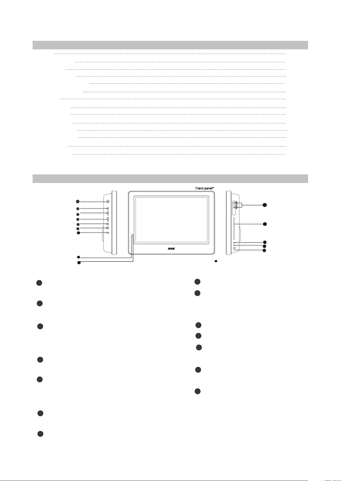
2.1.3 CONTROLS AND FUNCTIONS
(1) Panel controls and indication
1pcs
1pcs
2pcs
1pcs
1pcs
1pcs
1pcs
1pcs
1pcs
4pcs
4pcs
4pcs
1pcs
1pcs
6
1
2
3
4
5
7
8
9
Left panel
SETUP button
1
Press to switch to setup mode
2
_VOL+button
Press to adjust the volume.
_CH+button
3
Press to switch between channels/to
choose menu item.
SOURCE button
4
Press to choose the playback mode.
11
10
12
13
14
9
Front panel
8
Remote control sensor
9
Power supply indicator
Right panel
10
Disc tray
11
USB port
12
EJECT button
Press to open/close the disc tray.
13
STOP button
5
STANDBY button
Press to switch on the device/into
standby mode.
POWER button
6
Turn on/off the power.
7
Headphones output
- 5 -
Press to stop the playback.
PLAY/PAUSE button
14
Press to playback/pause.
Page 13
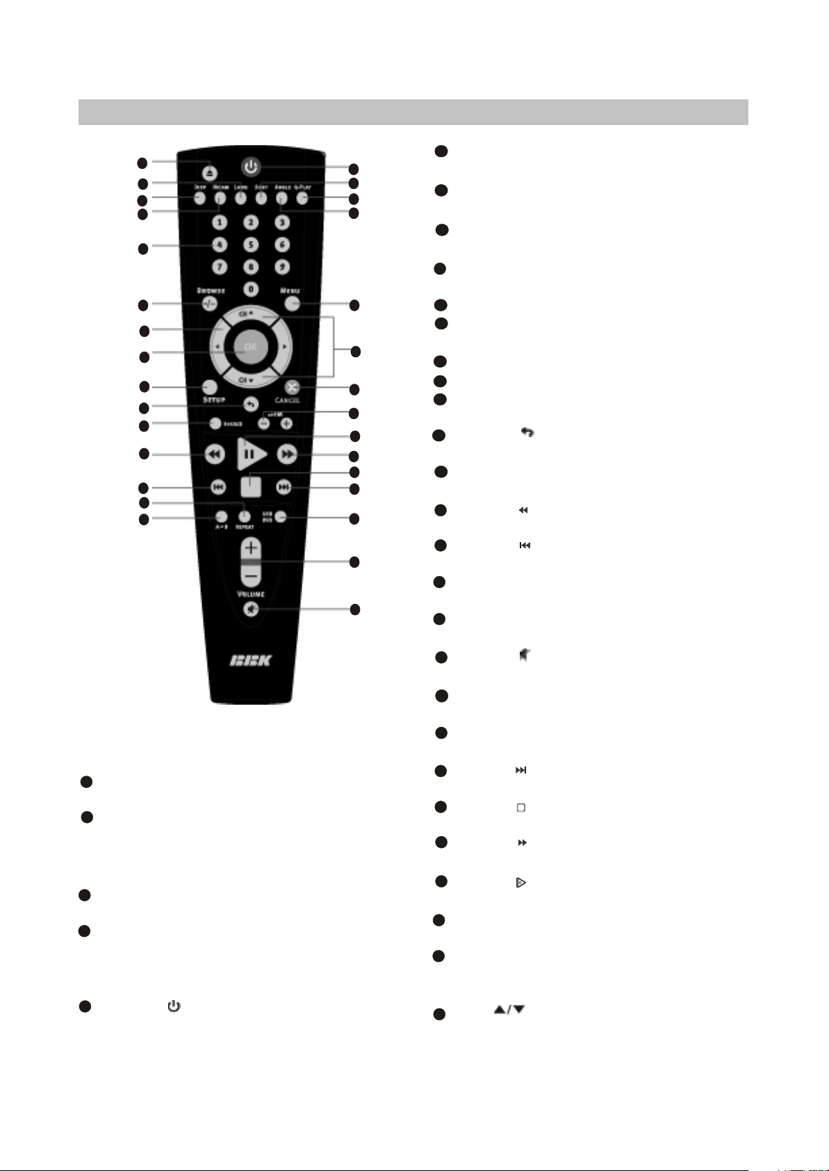
(2) Remote control general view
1
2
3
4
5
6
7
8
9
10
11
12
13
14
15
26
MENU button
DVD disk menu/PBC function.
27
ANGLE button
Press to change the camera
angle/change the Mp3 and JPEG files
playback mode.
28
Q-PLAY button
Press to turn the Q-PLAY mode on.
29
SUBT button
Press to change the subtitles
language/change the display mode JPEG
files.
30
Button
Press to switch on the device/into standby
mode.
1
EJECT button
30
29
28
27
Press to open/close the disc tray.
2
LANG button
Press to change language.
DISP button
3
Press to display the disc information.
NICAM button
4
Press to choose audio mode.
26
25
24
23
22
21
20
19
18
17
16
Numeric buttons
5
BROWSE button
6
Press to turn on/off the browser function.
CURSORbuttons(UP/DOWN/LEFT/RIGHT)
7
OK button
8
SETUP button
9
Press to switch to setup mode.
Button
10
Press to return to the previous channel.
SOURCE button
11
Press to change the TV/DVD mode.
Button
12
Press to start rewind/rewind scanning.
13
Button
Press to skip backward.
14
REPEAT button
Press to repeat.
15
A-B button
Press to repeat the selected section.
16
Button
Press to turn on/off the sound.
VOLUME+/-button
17
Press to adjust the volume.
18
USB/DVD button
Press to select USB/DVD mode.
Button
19
Press to skip forward.
20
Button
Press to stop the playback.
21
Button
Press to forward scanning.
22
Button
Press to playback/pause.
ZOOM+/-button
23
Press to zoom in/out.
24
CANCEL button
Press to go one level back/cancel current
operation.
CH button
25
Press to switch between channels /to
choose menu item.
- 6 -
Page 14
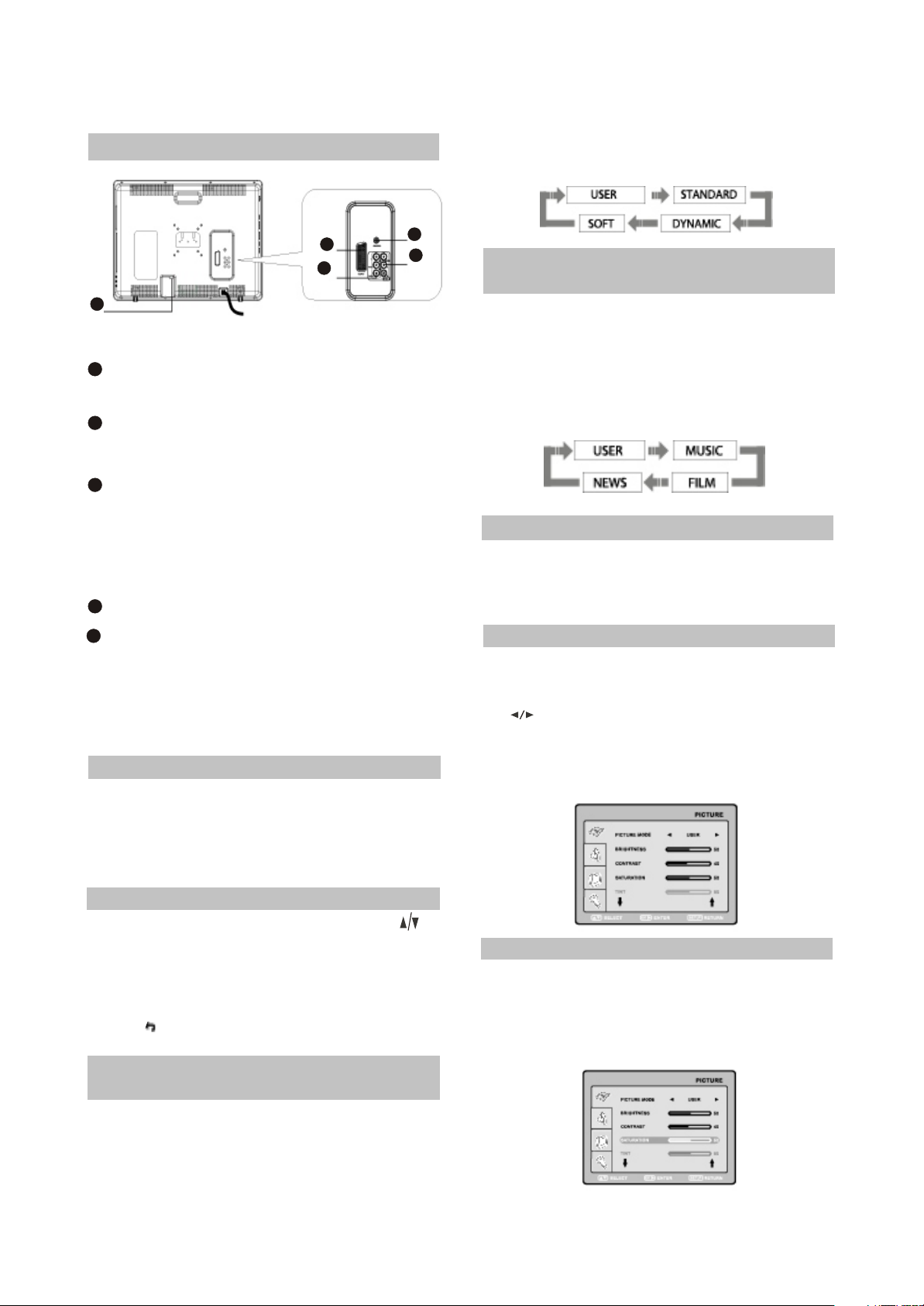
2.1.4 CONNECTION AND STARTING
SELECT RETURN
ENTER
SETUP
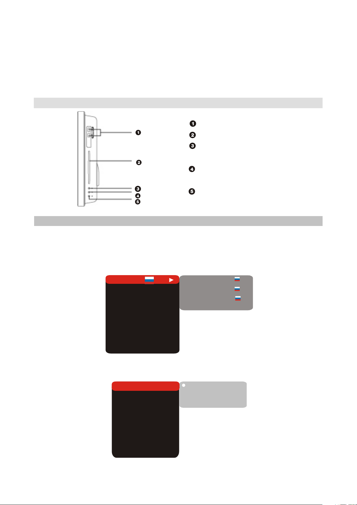
(1 )Switching interfaces
#You may adjust necessary parameters in the
device menu.
#Turn to Picture item on this page for details.
2
5
1
1
3
4
RF input
Meant for antenna connection.
2
COAXIAL OUT
Meant for multi-channel sound playback.
3
SCART socket
Meant for external audio video signal
source connection. There is no need to
use additional audiocord.
Y Cb(Pb) Cr(Pr)
4
AUDIO VIDEO IN
5
Used for external signal source
connection.
2.1.5
TV MODE
This LCD TV can store up to 100 channels and
enables to scan channels thought automatic,
manual and fine tuning scanning mode. Built-in
TV tuner supports stereo audio playback in
NICAM system.
(1) Adjusted channels selection
#Press +CH-buttons on the left panel or CH
buttons on the remote control each time, when
you want to change a channel.
#Use numeric buttons to enter the number of the
channel.
#Press button to return to the previous
channel.
(2) Default picture settings
selection
#You may select one of the default picture
settings:
USER, STANDARD, DYNAMIC and SOFT.
(3) Default sound settings
selection
#You may select one of the default sound
settings:
USER, MUSIC, FILM and NEWS.
#You may adjust necessary parameters in the
device menu.
#Turn to page.13 for details.
(4 )Accompanying sound type
#Only some of the TV channels have stereo
accompanying sound in NICAM system.
#Press NICAM button to select accompanying
sound.
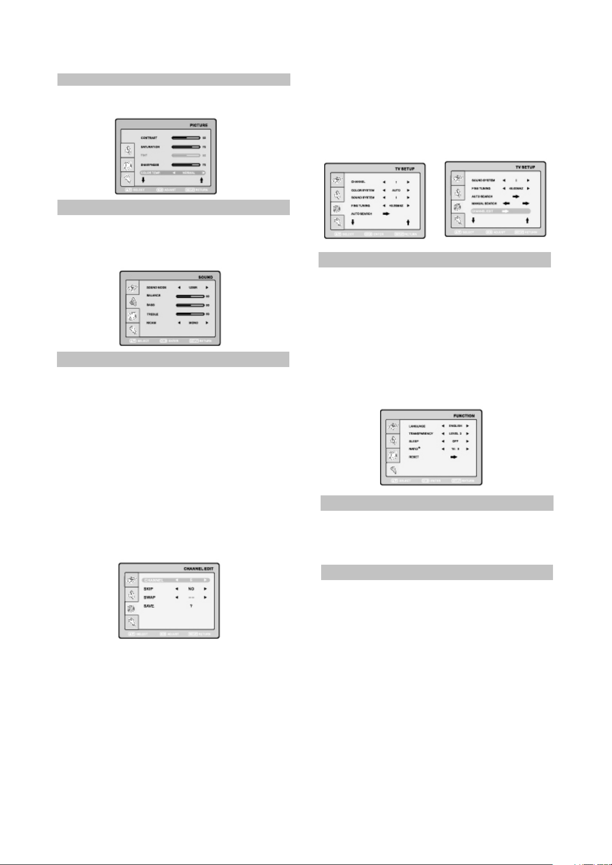
(5 ) TV settings
#Press SETUP button to display the menu.
#Use cursor buttons on the remote control or
+CH-buttons on the left panel to select the item.
Use buttons to adjust selected parameter.
Use OK button for confirmation. Press SETUP
button again to return to the main menu or to
exit TV SETUP.
(6) Picture
#select PICTURE item to adjust picture
parameters.
#You may adjust BRIGHTNESS, CONTRAST,
SATURATION, TINT, SHARPNESS and COLOR
TEMP.
- 7 -
Page 15
NOTE
You can’t adjust TINT while watching TV
channels.
(7) Sound
#Select SOUND item to adjust sound
parameters.
#You may adjust BALANCE, BASS, TREBLE
and NICAM.
(8) TV setup
Select TV SETUP item to adjust channels.
CHANNEL, COLOR SYSTEM, SOUND
SYSTEM, FINE TUNING, AUTO SEARCH,
MANUAL SEARCH and CHANNEL EDIT.
#CHANNEL item enables to select the number of
adjustable channel.
#CHANNEL EDIT submenu enables to select,
skip and swap the channel.
RETURN
SETUP
#CHANNEL parameter enables to select current
channel.
#SKIP function enables to make current channel
inaccessible while using +CH-button to browse
channels.
#COLOR SYSTEM item can be changed
between: AUTO, PAL and SECAM. We
recommend to set this item to AUTO.
#SOUND SYSTEM item can be changed
between: B/G, D/K, Land I.
(9) Function
You may select LANGUAGE, TRANSPARENCY,
SLEEP and RATIO.
#LANGUAGE item enables to select the OSD
language.
#TRANSPARENCY item enables to adjust
transparency of OSD.
#SLEEP item enables to set the sleep timer.
#RESET item enables to reset all values to
default.
(10) Video settings
#Press SETUP button to display the menu.
#In external video signal playback mode the
menu is the same as the menu, described on
pages 12and 13.
NOTE
In external video signal playback mode TV
SETUP item is inaccessible.
#SWAP function enables to select the channel
number to swap with current channel.
#SAVE parameter enables to confirm the swap
function.
#FINE TUNING item enables to adjust the
channel frequency accurately.
#MANUAL SEARCH item enables to change
channel settings.
#AUTO SEARCH item enables to adjust channel
setting automatically.
- 8 -
Page 16
Section Two DVD SEGMENT
2.2.1 Controls and functions
Two USB PORTS
Disc tray
EJECT button
Press to open/close the disc tray.
STOP button
Press to stop the playback.
PLAY/PAUSE button
Press to playback/pause.
2.2.2 FUNCTION SETTINGS
(1) Function selection and change
#Press the SETUP key to show the setup menu. You will see the following image on the screen, as show
on the figure:
#Select the desired menu item using the UP/DOWN buttons button; press the OK key for confirmation.
Language
Image
Sound
Playback
Preference
Parental control
Initial help
Reset settings
Exit
Setup menu
DVD menu
Sound track
Subtitle
Off
1.For example, if you wish to change the image settings, you have to select the image item and press
the OK or RIGHT key.
TV system
TV format
Sharpness
Gamma
Brightness
Contrast
Hue
Saturation
AUTO
4:3
M.
Off.
+48
+48
AUTO
PAL
NTSC
0
0
- 9 -
Page 17

2.Using the UP/DOWN buttons, select the
desired item and press OK or RIGHT button. For
example, select the Sharpness item. Settings
will appear on the screen. Then select the
desired sharpness level and press OK for
confirmation.
TV system
TV format
Sharpness
Gamma
Brightness
Contrast
Hue
Saturation
AUTO
4:3
Off.
+48
+48
High
L.
Medium
Low
Off
0
0
3. Press LEFT for exit to previous menu level.
4. Press SETUP to exit setup menu.
(2) Language settings
1. Setup menu: interface language set-up
#Options: Russian, English, Ukrainian.
#Default option: English.
Setup menu
DVD menu
Soundtrack
Sbutitles Off
2.DVD menu: selection of disc menu
language
3. Sound: selection of translation language
#Disc menu/translation language options:
Russian, English, Estonian, Lithuanian, Kazakh,
Romanian, Belarusian, Ukrainian, Chinese.
#Default menu/translation language option:
English.
#Selection of other languages: select the
OTHERS item using the wheel and press OK.
Enter the language code using the numeric
buttons and press OK.
#If the language you selected is not recorded on
the DVD disc, another available language will be
used.
4. Subtitles: selection of subtitles language
#Options: Off, Russian, English, Estonian,
Lithuanian, Kazakh, Romanian, Belarusian,
Ukrainian, and Chinese.
#Default option: off.
#Selection of other languages: select the
OTHERS item using the wheel and press OK.
Enter the language code using numeric buttons
and press OK.
English
#If the language you selected is not recorded on
the DVD disc, another available language will be
displayed.
(3) Image settings menu
1. TV system: TV system selection
#Options: Auto, PAL, NTSC.
#Default option: Auto.
2.TV Format: image ratio settings
#Options: 4:3 pan& scan, 16:9 letterbox and 16:9
TV,4:3 LB.
#Default option: 4:3 LB.
#Some discs are recorded with support of only
one ratio. The selected ratio must comply with
the TV screen.
TV system
TV format
Sharpness
Gamma
Brightness
Contrast
Hue
Saturation
Auto
4:3 LB
Off.
AUTO
PAL
NTSC
L.
0
0
0
0
3.Sharpness: image sharpness adjustment
#Options: High, Middle, Low.
#Default option: Low.
4. Gamma: adjustment of image color
temperature
#Options: High, Middle, Low, Off.
#Default option: Off.
5.Brightness: adjustment of image
brightness
6.contrast: adjustment of image contrast
7.hues: adjustment of image hues
8.Saturation: adjustment of image saturation
Adjustment of image brightness, contrast, hues
and saturation:
#Select the desired item of the image adjustment
section using the UP/DOWN buttons. Press OK
or RIGHT key to start adjusting the relevant
option.
#Change the option value using the wheel.
#Upon completion press the LEFT button of the
UP/DOWN buttons to return to image setup
menu.
(4) Sound settings menu
1.digital audio output
a).SPDIF format: set-up of digital audio
output options.
- 10 -
Page 18

#Options: RAW, PCM.
#Default options: RAW.
#When you select the RAW option, the not
decoded signal is transferred to the LCD Tv’s
digital outputs, the decoded signal is transferred
to analog outputs. Decoding is performed by the
built-in decoder of the LCD TV. This feature is
meant to ensure that signal decoding at digital
outputs is performed by an external
device(e.g.an amplifier).
#If you select the PCM option, a PCM coded
signal will be transferred to the LCD Tv’s digital
outputs.
Digital output
Tuning
SPDIF format
LPCM
RAW
48kHz
B)LPCM:set-up of digital audio output
options to comply with different amplifiers
and receivers.
#Options: 48kHz 16 bit, 96 Khz 24 bit.
#Default option: 48 Khz 16 bit.
2. Sound correction
A)Equalizer: equalizer modes
#Options: Off, rock, pop live sound, dance music,
techno classics, soft sound.
#Default option: off.
B)Echo: echo effects
#Options: Off, concert, living room, hall,
Bathroom, cave, arena, cathedral.
#Default option: off.
C)Tone balance: adjustment of tone balance
level.
#Adjust the tone balance level using the cursor
buttons.
#Press the LEFT button to return to sound
correction set-up menu.
(5) Playback settings
1. DVD
Advertisement skip: skip the unskippable
block while playing a DVD disc.
#Options: Yes,No.
#Default option: NO.
2. VCD/SVCD
PBS menu: PBC menu on/off
#Options: On, Off.
#Default option: On.
#If On option is set, while reproducing discs, a
menu will appear, in which you can select the
order of playing the disc content. If the Off option
is set, the reproducing of content is performed in
the order, in which it is recorded on the disc.
DVD
VCD/SVCD
Files
Repeat
All types
Advertisemenu No
off
3.Files: selection of reproduced files on the
disc
#Options: Audio, Pictures, Video, All types.
#Default option: All types.
4.Repeat: file repeat mode
#Options: Off, Single, All.
#Default option: Off.
(6) Preference settings
1.Screensaver: screen saver on/off
#Options: On, Off.
#Default option: On.
Screen saver
Equalizer
On
Off
On
Off
2.Equalizer: spectrum analyzer
#Options: On, Off.
#Default option: Off.
(7) Parental control settings
1.Category: set-up of age restrictions to
prevent children from seeing undesirable
discs.
#Options: Any, Kid, G,PG, PG-13, PGR, R,NC-
17.
any
Kid
G
Allowed..
Set password
Any
PG
PG-13
PGR
R
NC-17
2.Change password: set-up of a four-digit
password to change the level of age
restrictions.
#Default option: 7890
Old password
New password
Verify
OK
Cancel
(8) Initial setup menu
Auto
PAL
NTSC
- 11 -
Page 19

#Press the RIGHT key to enter the initial settings
Sign of trouble Cause of trouble Act ions t o ellminat e the trouble
No sound
1.Poor audio c able connec tion.
2.Disc dirty or damaged.
3.Sound disabled by the MUTE
button.
1.Mak e proper connect ion.
2.Clean the disc .
3.Pres s the M UTE button.
No image
1.Poor video cable c onnecti on.
2.Incorrect sett ings of your TV
set.
3.The TV is in the progressive
scan mode while y our TV set
does not s upport this mode.
1.Mak e proper connect ion.
2.Correct t he sett ings of your TV set.
3.Place the TV in the interlaced s can mode
through the TV's m enu.
Blac k and whit e image
1.incorrect TV c olor sy stem
selec ted.
2.Color level on the TV set
adjusted incorrect ly.
1.Set the appropriate c olor sy stem via the
menu: S ETUP>Image> TV sc an.
2.Readjust the c olor sy stem of your TV set.
menu, then select the desired item using the
cursor buttons and press OK key for confirmation.
#While being in this menu section, you cannot
return to the previous level by pressing the LEFT
key.
(9) Reset settings to default
Load factory settings
(10) Exit settings menu
Language
Image
Sound
Playback
Preference
Parental control
Initial setup
Reset to defaults
Exit
OK Cancel
#Select the exit item using the UP/DOWN
buttons and press the OK key to exit the menu.
#Resetting all settings and restoring default
options, except age restrictions level and
password.
2.2.3 OTHERS
(1) Useful notes
#To extend the service life of your LCD TV make pauses of not less than 30 seconds between switching
off and repeatedly switching on the LCD TV.
#Disconnect the LCD TV from the wall outlet after shutdown.
#Some LCD TV’S functions may not be applied to some discs.
#Use supply sources of rated voltage, otherwise the LCD TV may not function or be damaged.
#In case of the LCD TV’s occasional stops, please switch the power supply off and then on again.
(2)Trouble shooting
Please check probable causes of malfunction before addressing the service center.
- 12 -
Page 20
Disc s c annot be read
1.Disc not insert ed.
2.Disc ins erted inc orrectly.
3.Condensat e on the DVD
player's laser head.
1.Insert the dis c.
2.Install the di sc with t he label s ide facing up.
3.Switch the TV on without disc for an hour.
Microphone does not
operate
1.Microphone is unplugged.
2.Low level of the microphone's
sound volume.
1.Connect the mi crophone.
2.Adjust the level of the mic rophone's sound
volume.
Remote c ontrol does not
operate
1.Remote control is i ncorrect ly
direct ed at the TV's sc reen.
2.Distanc e to the TV i s in
excess of 8 meters.
3.Run out bat teries .
1.Use t he remote c ontrol ac cording to the
manual.
2.Decreas e the dis tanc e to the TV.
3.Replace both batt eries.
some functions do not
work
1.Disc is recorded inc orrectly.
2.Incorrect key s equence.
3.St atic voltage on the housing.
1.W ait5-10 s econds and the device will
automat ical ly t eturn to norm al state.
2.Repeat t he operation one more t ime.
3.Switch the device off for 1-2 min
Unstable image 1.Incorrect TV set set tings . 1.Correct the TV set set tings .
(3)Technical characteristics
LD1506SI LD1906SI LD2006SI
Type
class
Size(")
Height(mm)
Width(mm)
15
228.19
304.13
0.297×0.297
19
256.5
410.4
0.285×0.285
20/50,8
306
408
0,707×0,707
Frequency
Vertical(Hz)
Horizontal(kHz)
Display color
Maximum Display
Mode
Resolution
Vertical frequency(Hz)
1024×768
75
1440×900
75
640×480
75
Inputs
Video
Composite
Component
VGA
RGB/SCART
Audio
Stereo
PC audio
Others
USB
RF
1
1
1
1
2
1
2
1
1
1
1
1
2
1
2
1
1
1
1
2
-
2
1
Audio outputs
Headphone
Digital coaxial
1
1
1
1
1
1
TFT,colored
ll(ISO 13406-2)
Display
50-75
30-75
16 700
- 13 -
Page 21
Color system
TV tuner
Video inputs
Sound system TV tuner
Disc types
Formats
:+12 :+12 -
Power supply
Power Consumption
(Maximum)(w)
Power Consumption
(Power Saving)(w)
65
<3
Environmental
consideration
Operating temperature(°,C)
Operating humidity(%)
Storing temperature (°,C)
Storing humidity(%)
Dimensions(mm) 438.7×295.7×73.4 498×370.6×82.5 620×450×202
Weight Net weight(kg) 6.5 7.1 8.1
54
<3
+5 +35 10-80
-20 +45
CD-R/RW,DVD-R/RW,DVD+R/RW
DK,I,BG,L
Built-in DVD
player
DVD-Video,DivX,XviD,SVCD,VCD,CDDA,HDCD,MP3,WMA,Kodak Picture CD,JPEG
~100-240,50/60
Voltage and
frequency(V,Hz) Voltage of
external(V,A)
Power adapter
PAL,SECAM
PAL, SECAM, NTSC 3.58, NTSC 4.43,PAL60
#We are permanently improving the quality of our products; hence the product’s design, functionality
and technical characteristics may be modified without prior notice.
#We do not guarantee that all discs can be played smoothly due to the disc quality, disc recording quality
and recording format.
- 14 -
Page 22

Chapter Three Principle and Servicing
The previous manual: TV part
Section One Principle of the player
3.1.1 Function
LD2006SI is a 20” LCD_TV with multiple functions, such as DVD playing and USB reading function.
Electronic scheme of TV part adopts 20” TFT display screen+inverter components
(INV604)+MST718+STV8216 +TDA7266P+ tuner JS -6H2/T121. MST718 includes MCU/video A/D
converter/LCD image processing circuit. DVD part electronic scheme adopts MT1389HD+64M
SDRAM+16M FLASH+D5954. HD62 loader can smoothly read MPEG4/MP3/CD/DVD format discs and
decode chip MT1389HD may support USB and card read function.
# Digital picture adjustment technology to adjust sharpness, brightness, contrast, hue and
saturation of pictures; gamma correction.
# Video circuit supports PAL/NTSC/SECAM/PAL60 multi-system video signals.
# Support USB/card read function.
# Compatible with DIVX, MPEG4 format film.
# Support PAL BG/DK/I, SECAM BG/DK/L/L’ RF signal modulating.
3.1.2 Block diagram of the player
3.1.2.1 This machine is mainly composed of the following PCB semi-finished products and display
screen components. Please refer to model list for allocation of the player:
1. Main video board (21903-4): this PCB semi-finished product is the main part of the player. Main
video board includes audio/video input circuit, audio selecting and amplifying circuit, video selecting and
LCD drive circuit, DVD decode and servo circuit. The main function is to fulfill audio/video signals’
processing and DVD function’s fulfilment.
2. Power board (@52006-0UL): power board is mainly composed of rectifying circuit and filtering
circuit. This PCB semi-finished product’s main function is to provide the player with working power.
- 15 -
Page 23
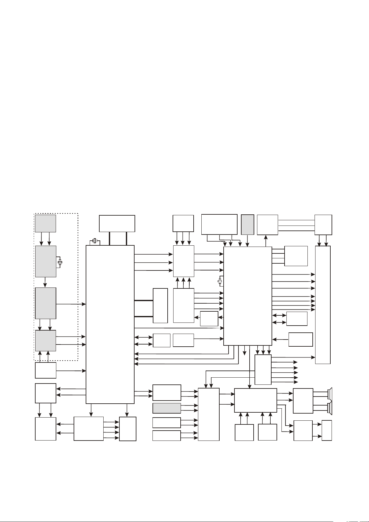
3. Inverter components (INV607): inverter components are mainly composed of boost circuit and
protection circuit. This PCB semi-finished product’s function is to provide display screen components
with lamp working voltage.
4. Remote control receiving board (B1903-1): this semi-finished product is composed of one IR
sensor and working indicator light. This PCB semi-finished product’s main function is receive the control
order that sends from remote controller and transmit to MCU part of main video board to control the
working state indication of the player.
5. TV button board 41903-0/DVD button board J1903-0: mainly composed of buttons which are
responsible for the function control of TV part and DVD part.
6. USB board D1903-1: this PCB semi-finished product includes USB jack circuit and it is mainly
responsible for USB read function.
7. Display screen components: include LCD display screen, lamp, LCD screen drive circuit and jack
circuit. The main function is to revert video signals to image to supply for clients to enjoy video images.
TUNER
If1
If2
U119
PN2020
TSDATA0~TSDA TA7
U116
MT8606
XIDD0
XIDD8
DVB/CARD
switch
U108/U2
MSD0
MSD1
CRAD
BOARD
OPEN/
CLOSE
circuit
LOAD+
LOAD-
DVD
LOAD
DVB part
20.48MHZ
X602
XIDD0~XIDD15
GPIO_3
GPIO_4
TROPEN
TRCLOSE
FOSO
TRSO
FMSO
DMSO
SL+
SL-
Servo drive
U302
DVD
X109
27MHZ
FLASH
DFA[0:20] DFD[0:7]
Mt1389
DVD decode
chip
39
54
TK+
Ba5954
U118
TKFC+
FC-
109
98
100
226
224
A/B/C/D/E/F
DVD
PICK_UP
DY
DPB
DPR
DDQ[0:15]
DMA[0:11]
DSCL
DSDA
89AL
89AR
Y PB PR
INPUT
JACK
EPR
Video
Electronic
switch
FSAV433
SR SGSB
U301
SDRAM
DCVBSIN+/DCVBS-
EEPROM
U303
24C16
4580
U117
Audio
amplifying
circuit
23
U113
TEA5764
24
SCART JACK
J105
AV input terminal
EY
U106
SCART
JACK
TUNER
DVSTB
DVSCK
DVSDA
DRIN
DLIN
FMR
FML
SRIN
SLIN
AVRIN
AVLIN
EPB
PRIN
PBIN
Y
12MHZ
SCVBS+
SCVBS-
SCLTX
SDARX
Video
amplifying
circuit
TV+/TV-
U107
Electronic
switch
Cd4052
key-press board &
receiving board of
remote control
KEY2
X101
IR
KEY1
7/8
9/10
12/13
24
25
67
66
34
22/23
30/31
73 83
63
Vs1
Vs2
8216_RST
AI3L
13
AI3R
3
PCLIN
Boost
VGA
control
JACK
circuit
U101
MST718
LCD
image
processor&
MCU
74
60
T4094
VSDA
PANEL_ON
1
U102
CD4094
23
U111
NICAM processing
circuit
24
STV8216
15
14
PC AUDIO
J103
73
PCRIN
SIOMAD
Brigtness
BLON
+12V
INVERTER_ON/OFF
SPICK
SPIDI
U104 FLASH
SPIDO
PS25LV010
SPICZ
DG0~DG7
DB0~DB7
DR0~DR7
HSYNC
VSYNC
DE
CLKO
MST_RESET
VSCK
SEL_I/P
3
2
AMP_STB
ANT-POW
ASW
MUTE
ONMUTE
LSL
28
LSR
29
18
19
9/10
AO2L
MONOIN
TUNER
U114
AO2R
U103
EEPROM
24C32
Reset circuit
Q103 Ce101
4
Audio
12
amplifying
TDA7266
Audio
output
amplifying
circuit
INVERTER
BOARD
PANEL
1
2
15
14
SCART
figure 3.1.2.1 Block diagram of the player
- 16 -
Page 24
Annotate: 3.1.2.1 Block diagram explanation: this machine is divided to 3 parts according to
SN Material code Material name Specs & Model Qty
Position
Number
Function
1 790021 FET IRF7416 SOP 1 U511 (+)12V switch control pipe
2 883191 IC TDA7266SA ZIP 1 U112 Audio amplifying IC
3 882030 IC STV8216 TQFP 1 U111 NICAM processing IC
4 883189 IC MST718BE PQFP 1 U101 LCD image processing&CPU
5 883323 IC AP1506Adj TO263-5L 2 U503,U506 (+)5V voltage stabilizing IC
6 882953 IC K4S641632K-UC60 TSOP 1 U301 SDRAM
7 882076 IC LM1085-3.3 SOT-263 1 U521 DV33 voltage stabilizing IC
8 882883 IC FSAV433 TSSOP 1 U106 Components video selection IC
9 790126 SMD FET FDS9435A SOP 1 U502 Display screen power control pipe
10 880504 IC 24C32N SOP 1 U103 TV EEPROM
11 882756 IC HEF4094BT SOP 1 U102 Serial/parallel converter
12 882515 IC HEF4052BT SOP 1 U107
Sound source selecting electronic
switch
13 882485 IC AZ1117H-3.3 SOT-223 2 U505,U513 3.3V voltage stabilizing IC
14 883245 IC AZ1085S-2.5Z TO-263 1 U507 2.5V voltage stabilizing IC
15 882121 IC AK18 SOT-223 1 U1 1.8V voltage stabilizing IC
16 1020094 Tuner JS-6H2/T121 1 U114 Receive TV signal
17 900458 Software program ROMLD2006SI2-0A(2M) 1 U104 TV software program
functional module.
1. TV part: according to design demands, TV part mainly includes LCD image processing, audio
processing and amplifying circuit, MCU control circuit.
2. According to design demands, DVD part mainly includes decode circuit and servo circuit.
3. DVB circuit: DVB circuit mainly includes channel decoder and TS decoder. This machine does
not use this function, to facilitate understanding, so we use gray colour to mark the unused part in the
block diagram.
3.1.3 Function introduction to IC of the player
Function introduction to IC of the player is shown as in the following figure:
- 17 -
Page 25
Section Two Unit Circuit Principle
3.2.1 System control circuit
System control circuit is mainly composed of reset circuit, clock circuit t, serial/parallel conversion
circuit, software program, EEPROM and MCU (MST718 is built inside). The built-in MCU of MST718 is
mainly responsible for the coordination and control of system of the player. This MCU is connected with
a 2M ROM externally, which is used to store software and control function of the player. Since I/O port of
MST718 is limited, a serial/parallel conversion circuit (CD4094)is added to extend I/O port. Functions
may be adjusted through software. MST718 is connected with a 32k EEPROM externally, used to store
user-set information.
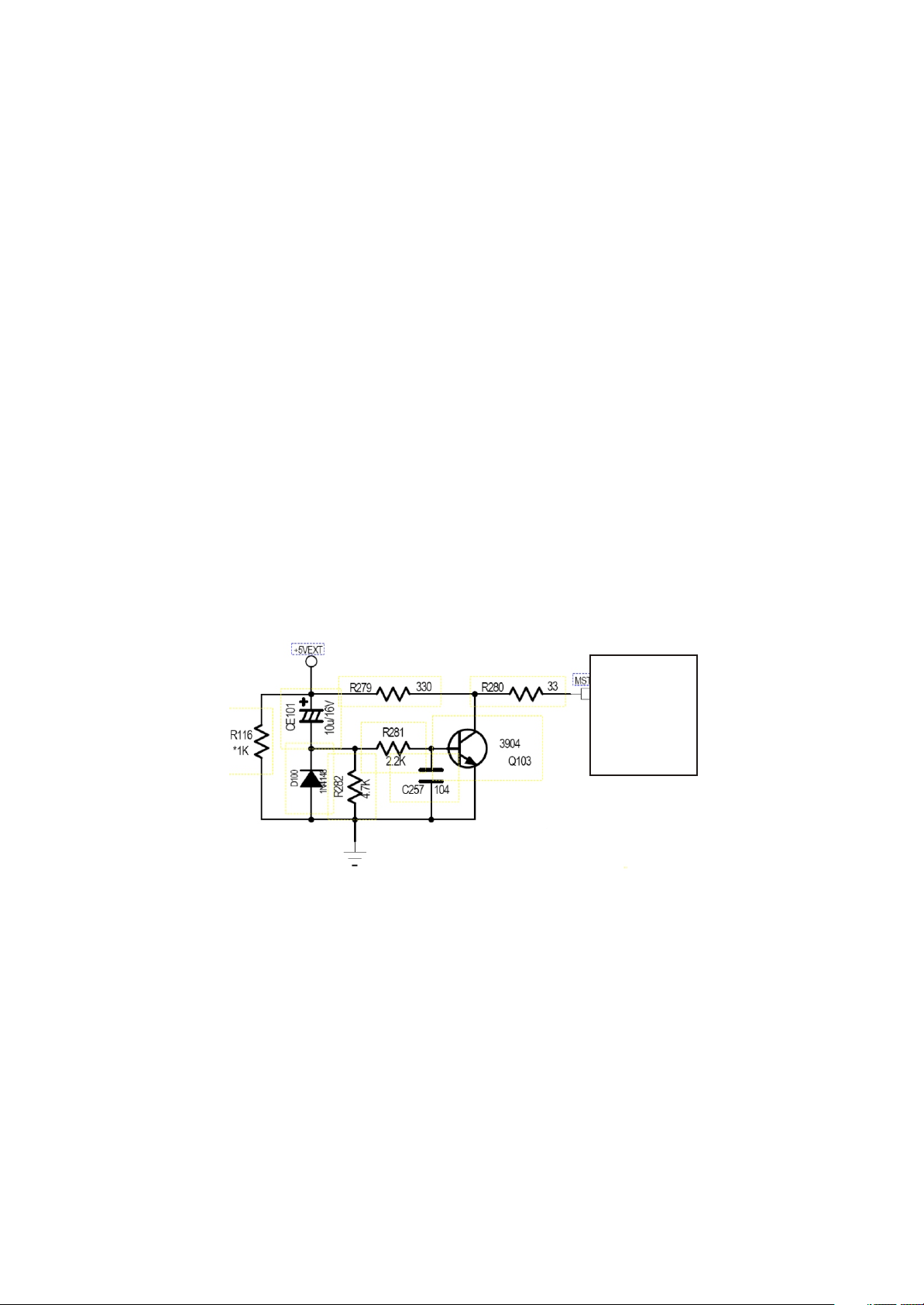
1. System reset circuit
(1) system reset circuit is shown in the figure 3.2.1.1:
68
MST718
Figure 3.2.1.1 System reset circuit diagram
(2) Working principle: this circuit is a typical low level effective reset circuit. After power on, “+5V
EXT” changes from 0V to 5V,and charge R282 through CE101,Voltage of two ends of CE101cannot
change suddenly, now Q103 is saturated on, C-E electrode is connected, MST RESET is low level to
provide pin 68 of U101 with a low level reset signal to reset MST718. After capacitor CE101 is fully
charged, voltage on two ends is near to 5V, now Q13 cuts off, voltage of pin 68 of MST718 restores to
high level to finish reset action.Reset time of this circuit is about 100MS, which is decided by the value
of R282 and Ce101. Function of D100 is to discharge Ce101 quickly to ensure the reliable reset when
power on for the second time. The trouble that appears in this circuit is that machine cannot enter
standby state after power on, and machine fault after power on.
- 18 -
Page 26
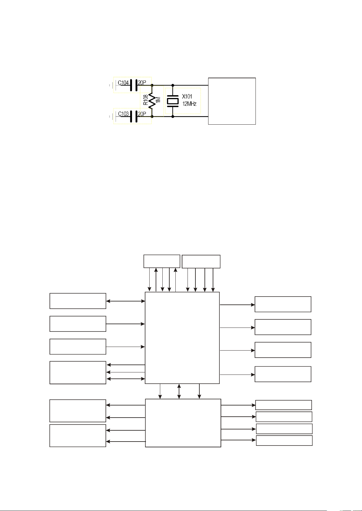
2. System clock circuit
(1) System clock circuit is shown in the figure 3.2.1.2:
120
MST718
121
Figure 3.2.1.2 System clock circuit
(2) Working principle: this clock circuit is mainly composed of X101, C104 and C103, in which X101
is a 12MHZ crystal oscillator; C104 and C103 are externally-connected resonance capacitors to produce
a 12MHZ clock signal to provide for MST718 to generate clock signal required by system through
internal doubling circuit to act as working clock.
3. System control principle
(1) System control schematic diagram is shown in the figure 3.2.1.3:
Key-press board
Reset circuit
Remote control board
MT1389HD
KEY1~KEY5
RESET
IR
DVSTB
DVSCK
DVSDA
U104
PS25LV010
Z
DI
O
C
I
I
ID
SP
SP
SP
T4094
SCART JACK
K
S
P
S
PIC
W
S
MST718
MCU
VSDA
FB
VSCK
X
CLT
S
X
SDAR
INVERTER ON/OFF
STBY
8216_RST
PANEL_ON
Inverter components
power control circuit
STV8216
PANEL_ON
control circuit
U107
Cd4052
Audio input selection
Mute control circuit
Vs1
Vs2
U102
MUTE
Cd4094
Serial/parallel converter
ONMUTE
Figure 3.2.1.3 System control schematic diagram
- 19 -
ASW
ANT-POW
AMP_STB
SEL_I/P
U109/CD4053
DVB/TV
Tuner power control circuit
TDA7266 audio amplifying
LCD_TFT
Page 27
(2) Working principle
System control circuit of the player is composed of the built-in MCU of MST718 and software
Program. Machine power on: after 12V power is being rectified by U503, +5V power outputs to provide
for system control circuit. The reset circuit of system control circuit begins to reset MST718, the red
indicator light on remote control receiving board is on under the control of STBY signal (high level), and
this means machine enters standby state.
The process from standby state to power on state: after pressing POWER button on panel or wake
code on remote controller, pin 57 of MST718 changes from high level to low level, pin STBY outputs a
low level signal to make Q117 cutoff, /STBY skips to high level, STBY is divided to 3 parts: +5V power
control circuit composed of Q3/U506; +12V power control circuit composed of Q117/U511 and standby
indication circuit on remote control receiving board. Power supply of machine is normal, MST718 begins
to output reset and other control signal (please refer to waveform diagram for sequence of each control
signal output) to reset and control circuit of other module to make machine enter normal working state.
The process from working state to standby state: when machine is in power-on state, after
pressing POWER button on panel or wake code on remote controller again, machine enters from power-
on to standby, now pin 57 of MST718 outputs high level, /STBY pin output low level, +5V power and
+12V power of machine are cut off and machine enters standby state.
4. IIC bus control circuit
(1) IIC bus control circuit block diagram is shown in the figure 3.2.1.4:
U101
MST718
TUNER
SDA
SCL
U103
24C32
Ic301
STV8216
Figure 3.2.1.4 IC bus control circuit block diagram
U119
PN2020AT
U113
TEA5764
(2) Working principle: IIC bus is a kind of simple, dual-direction and synchronous serial line
developed by PHILIPS company. Only 2 lines (serial clock line and serial data line) are required to
connect between components on bus to transmit information. This bus is high-performanceserial bus
which has function of decision and synchrony of high and low speed devices required by multi-player
system with wide application range. shown in the figure 3.2.1.4, U103 is a 32K memorizer used to store
user information.
- 20 -
Page 28
5. Serial/parallel conversion circuit
(1) Serial/parallel conversion circuit is shown in the figure 3.2.1.5:
SEL_I/P
AMP_STB
ANT_POW
ASW
Vs1
Vs2
MUTE
ONMUTE
MST718
MCU
T4094
VSDA
VSCK
Figure 3.2.1.5 Serial/paralle conversion circuit
Serial/paralle
converter
Cd4094
(2) Working principle:
Because jack of MST718 is limited, in order to extend control port, a serial/paralle converter
(CD4094) is added in MCU peripheral. CD4094 is a serial in/paralle out high speed converter with output
latch and 3-mode control and its advantages are easy usage, low power consumption, strong drive and
flexible control. {1} pin is latch end, {2} pin is serial data input end, {3} pin is serial clock end. When {1}
pin is high level, the increase of 8-bit paralle output port Q1~Q8 changes with serial input; when {1} pin
is low level, output is locked. Using latch end may conveniently perform chip selection and output control.
{15} pin is parallel output state control end, when {15} pin is low level, parallel output end is in high
resistance state; when using CD4094 as display output, the display number may flicker. QS of pin {9}
and Q’S of pin {10} are serial data output end. Control signals after conversion are used in control mute
circuit/sound source selection circuit.
6. Working state indication circuit
(1) Working state indication circuit is shown in the figure 3.2.1.6:
Figure 3.2.1.6 Working state indication circuit diagram
- 21 -
Page 29
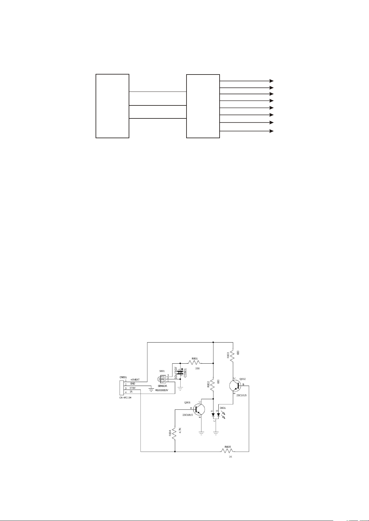
(2) Working principle: when machine is in standby state, pin 57 of MST718 outputs high level signal
To make standby control circuit \STBY signal outputs low level signal. This signal is directly connected to
pin 3 of remote control receiving board flat cable holder Cn801. This control signal inputs to base
electrode of Q801/Q802 through R804/R805 to make Q802 cutoff, Q801 is connected, the red light of bi-
color diode D801 is on, which means that machine enters standby state. After pressing POWER button,
machine enters working state, pin 3 of ,Cn801 outputs high level to make Q802 on/Q801 cutoff, the
green light of b-icolor D801 is on, which means machines enters working state. S801 is IR sensor to
receive remote control signals mainly.
3.2.2 Audio circuit
Audio processing circuit is mainly responsible for the switch, amplifying and restire of audio and
composed of audio source input selection and NICAM processing circuit, audio amplifying circuit and
mute control circuit. Audio processing circuit block diagram is shown in the figure 3.2.2.1:
PC AUDIO
J103
TUNER
U117 4580
AV_IN J105
SCART JACK
DRIN
DLIN
AVRIN
AVLIN
SRIN
SLIN
PCLIN
PCRIN
MONOIN
SIOMAD
CD4052
Electronic
switch
Figure 3.2.2.1 Audio processing circuit block diagram
1. “Nicam” processing circuit
13
73
78
Multi-channel
audio selection
9
10
NICAM signal
processing
Ic301
AI3L
AI3R
3
Vs1
Vs2
STV8216
23
24
CD4094
28
29
LSL
LSR
4
TDA7266
Audio
amplifying
12
Audio output
amplifying
circuit
1
2
15
14
Headphone
socket
(1) NICAM: the core technoloy of “NICAM” is the NICAM728 technology developed by BBC.
Besides transmitting TV image and simulating mono-channel signal, NICAM TV broadcasting system also
transmits dual-channel digital coding sound signal. NICAM is famous for clear treble and deep bass with
the sound quality close to listeing to CD disk directly. In the aspect of SNR, dynamic range and channel
separation index, NICAM is far better than the current FM accompany. As TV accompany, NICAM
applies 3 kinds of working mode currently: 1) Bilingual mode: NICAM transmits dual-channel digital
sound relevant or irrelevant to the current program and transmits 3-channel sound signal together with
- 22 -
Page 30

The original FM analog accompany, which are suitable for multi-language areas; 2) Stereo mode: two
digital channels of NICAM transmit left and right channel sound signals of stereo separately, and the
original FM analog accompany only transmits mixed sound signals of 2 channels to be compatible with
TV set without NICAM function; 3) Mon0-channel mode: two channels of NICAM transmit one channel
sound signals and one channel data signal, which is equal to providing 3-channel signals together with
the original TV analog accompany.
(2) “NICAM” processing circuit: when tuner receives NICAM signal, it outputs from pin 11 of tuner
(SIOMAD), and inputs into pin 73 of STV8216 through the filtering circuit composed of C301, C302
components and then restores to audio signal through being modulated by internal circuit of STV8216
and sends to audio amplifying circuit through pin 28, 29 of STV8216. STV8216 block diagram is shown
in the figure 3.2.2.2:
Figure 3.2.2.2 STV8216 internal block diagram
2. Sound source input selection circuit
Besides NICAM processing circuit, STV8216 also includes multi-channel sound source selection
function. After the machine enters from standby to power-on, systems sends a low level effective reset
signal to pin 43 of STV8216 to reset STV8216. IIC bus means is adopted between STV8216 and
MST718 for communication. When system working state is set in SCART input, Cd4052 outputs SCART
signal under the control of MST718 and then input to STV8216, now pin 23, 24 of STV8216 output the
audio signals inputted by SCART_IN and also output two groups of audio signals as external output
signal through pin 18, 19. Working principle of other groups’ sound source input is the same, so we will
not introduce here.
External input sources of this player are many and input port of STV8216 cannot meet the demands,
so a CD is added in front of STV8216 to switch in DVD_AUDIO/external input terminal and SCART
AUDIO input port.
- 23 -
Page 31

3. Audio amplifying circuit
(1) Audio amplifying circuit is shown in the figure 3.2.2.3:
Figure 3.2.2.3 Audio amplifying circuit diagram
(2) Working principle: TDA7266P is a 3W+3W dual-bridge audio amplifying. Audio signals input
through pin 4, 12 of TDA7266 and then output from pin 1, 2, 14, 15 of TDA7266P after being amplified
by internal dual-bridge audio amplifier to drive loudspeaker to make sounds. This IC adopts +10V power
supply, D122/D123 is drop diode and pin 7 is standby control pin. After machine enters power-on state,
pin 12 of cd4094 (AMP_STB) outputs high level and this IC enters working mode. This player adopts
default high level mode, so R22 is not used, but R28 is adopted to connect onto power. Pin 6 is mute and
controlled by mute circuit.
4. Mute control circuit
(1) Mute control circuit is shown in the figure 3.2.2.4:
Figure 3.2.2.4 Mute circuit diagram
Òô¿ØÖƵç·ͼ
- 24 -
Page 32

(2) Working principle
Power-on mute: after power on, machine enters from standby to power on. Because of R28, pin 11
of TDA726P is low level, now ONMUTE pin of Cd4094 outputs high level signal, OUTMUTE is high level,
,Q113/Q112/Q119 is saturated on, machine enters mute state to realize power-on mute effect. After
machine starts up, ONMUTE switches to low level, Q113/Q112/Q119 cuts off to make pin 6 of TDA7266
high level, TDA7266 enters non-mute mode, the player has sound output and power-on mute fulfills.
Power-off mute: when machines enters standby mode from working state, ONMUTE pin outputs high
level, OUTMUTE pin is high level signal, TDA7266 enters mute state.
Power failure mute: when power of machine is switched off, Ce151 has been fully charged when power
on, after machine power switches off, Ce151 discharges through Q118/D121 to make Q119 connected,
now pin 6 of TDA7266 is low level to realize power-off mute function.
When user use remote controller to mute the machine, MUTE pin outputs high level signal to make Q119
saturated on, pin 6 of TDA7266 is low level and TDA7266 enters mute mode.
(3)SCART Audio output amplifying circuit:
SCART Audio output amplifying circuit is shown in the figure 3.2.2.5:
Figure 3.2.2.5 SCART Audio output amplifying circuit diagram
Working principle: the picture is an amplifying circuit composed of triode, mainly used in audio
output amplifying. Q114/Q115 in the picture is amplifying pipe,CE131/CE130 is blocking capacitor,
Q113/Q112 is mute pipe which is used for power on/off mute. Audio signals outputted by this circuit are
used for SCART output.
- 25 -
Page 33

3.2.3 Video circuit
Video circuit is mainly responsible for the input of external video signals, the processing of video
signals send from tuner, and the drive processing of LCD screen, including video input selection, video
A/D conversion circuit, LCD picture processing circuit and video output circuit. Video circuit block diagram
is shown in the figure 3.2.3.1:
Y PB PR
INPUT
JACK
Mt1389
EY
EPB
EPR
DY
DPB
DPR
U106
Video
Electronic
switch
FSAV433
SR SGSB
SCART
JACK
DCVBSIN+/DCVBS-
PRIN
PBIN
Y
X101
12MHZ
SCVBS+
SCVBS-
SCLTX
SDARX
video
amplifying
7/8
9/10
12/13
24
25
67
66
34
22/23
U101
MST718
LCD picture
processor&
MCU
30/31
DG0~DG7
DB0~DB7
DR0~DR7
HSYNC
VSYNC
DE
CLKO
TV+/TV-
PANEL
TUNER
Figure 3.2.3.1 Video circuit block diagram
1. Video input and video processing circuit
His circuit is mainly composed of FSAV433 and MST718, MST718 supports NTSC, PAL and
SECAM video signals and the supportable video signal format has RGB, YPbPr, CVBS or S-video video.
The built-in A/D converter can realize multi- format’s conversion function. MST718 adds video switch,
A/D converter and MCU on the basis of MST518 and MST718 also has video output function. Output jack
includes TTL, LVDS modes.
When machine is set in DVD or DVB mode, Y PB Pr signal is inputted to pin 2/6/10 of FSAV433,
and then output from pin 13/15/17 after being selected through electronic switch (FSAV433) to MST718
for A/D conversion. At the same time, Mt1389 also outputs composite video signal, after being selected
through the internal video electronic switch of MST718, output from pin 34 of MST718 to the video
amplifying circuit composed of Q100, Q1 and then output to SCART video output pin.
- 26 -
Page 34

2. LCD image processing circuit
Pin Name
Signal
direction
Function description Pin Name
Signal
direction
Function description
1 A(B)OUT I Audio right channel input 12 NC Networ k commun ication dat a lin e 2
2 A(B)IN O Audio right channel output 13 RETURN Pr signal ground
3 A(A)OUT I Audio left channel input 14 RETURN Blanking signal ground
4 A-COM Audio signal ground 15 RED I/O I/O Pr signalI/ O port
5 RETURN Pb signal ground 16 BLK I/O I/O
Blanking signal I/ O port
6 A(A)IN O Audio left channel output 17 RETURN Blanking signal ground
7 BLUE I/O I/O Pb signalI/O port 18 TRTURN Composite video signal ground
8 FUNCSW I Function selection jack 19 V-OUT I Composite video signal input
9 RETURN Y1 signal ground 20 V-IN O Composi te vid eo sig nal output
10 CONT I/O
Networ k commun icat ion dat a
line 2
21 GND Common
11 GREEN I/O I/O Y1 signal I/O port
LCD image processing circuit is composed of MST7187 And peripheral elements, Responsible for
switching the exterior inputted analog video signals into signals required by LCD drive.
MST518 is a high-performance and high integration picture processing chip designed for LCD,
which can support SXGA format. multi-format output display jack (support TTL, LVDS, RSDS). This
player adopts analog signal, MST718 built-in MCU, MST518VA has multi-format output display jack. TTL
output means is adopted in this player and the output means can be adjusted through software
according to screen’s drive means.MST7187outputs DR0~DR7/DG0~DG7/DB0~DB7 to drive display
screen, and also outputs clock, enable and synchronous signals to supply for the working of screen (770
OCLK clock output, 78 DE enable signal, 79 VSYNC filed synchronous output and 80 HSYNC line
synchronous output).
3.2.4 Input circuit
External input means of TV has SCART\CVBS and Y/PB/PR, and also composite video and stereo
audio output function.
1.Introduction to SCART terminal :
SCART terminal is a standard input port in Europe. In this jack circuit, many dual-direction diodes
are adopted and act as protection function to prevent the instability of externally-conected device or
damage of the machine due to static. SCART pin function is shown in the following table:
- 27 -
Page 35

2. TV Tuner circuit
Pin Name Function Pin Name Function
1 NC NC 8 NC DVB input jack is unus ed
2 VT Connect with external power 9 NC NC
3 VS (+)5V power supply pin 10 NC NC
4 SCL SCLis connected with MCU 11 SIF SIOMAD
5 SDA SDA is connected with MCU 12 TUNER_CVBS Video output
6 AS AGC control end is unused 13 VIF
5V power is connected
externally
7 AFC DVB input jack is unus ed 14 AUDIO Audio output
(1) Tuner circuit is shown in the figure 3.2.4.1
Figure 3.2.4.1 Tuner circuit diagram
(2) Working principle: this tuner includes middle frequency amplifying circuit, which adopts IIC bus
means to perform function control (such as select channel and search channel) through MST718 built-in
MCU. After high frequency signals are modulated, video signals and audio signals are separated
through being filtered by internal filter of tuner. Audio and video signals output from pin 12, 14 and then
send to audio and video processing circuit. When tuner receives NICAM signal, NICAM signals output
From pin 11 of tuner to STV8216 for modulating.
(3) Tuner pin function is shown in the following table:
- 28 -
Page 36

3.2.5 Power circuit
1. Power circuit block diagram
(1) Power circuit supplies stable and pure power for each unit circuit to ensure normal working of the
player. Power circuit block diagram is shown in the figure 3.2.5.1:
IC 503
AP1506
U511
+12V
Power Board
Standby
control circuit
AP1506
U506
INVERTER
BOARD
U502
Si9435
Figure 3.2.5.1 Power circuit block diagram
+5VEXT
+12V
STBY
5V
FOR PANEL
U505
AMS11 17
U507
Lm1085
MST718
U513
U1
AMS1117
U521
Lm1085
3.3V
+2.5V
MST718
+3.3V
1.8V
Dv33
(2) Working principle: after AC power is being rectified and filtered through power board, 12V power
outputs. This power is inputted to voltage stabilizing circuit of video main board through socket Cn6 for
voltage stabilizing. The power outputted after being voltage stabilized is working power of each circuit.
Voltage stabilizing circuit on video main board is divided to 3 parts: 1) +5VEXT outputted after being
voltage stabilized by Ic503 is mainly supplied for system control circuit; 2) +5V power outputted after
being voltage stabilized by is mainly supplied for DVD/DVB circuit; 3) +12V voltage stabilizing and
control circuit supply working voltage for rear audio circuit.
(3) Introduction to each functional module in the picture: U502 is display screen power control pipe,
controlled by PANELON signal outputted by MST718; U511 is 12V power control pipe; U505/U507 is
voltage stabilizing IC, which supplies working power for MST718; U516/U1/U521 is voltage stabilizing
IC and voltage outputted after voltage stabilizing is supplied for DVD circuit. Please refer to the following
part “Principle analysis” for working principle.
2. +5VEXT
(1) +5VEXT
the figure
Voltage stabilizing circuit and display screen Power control circuit
Voltage stabilizing circuit and display screen Power control circuit diagram is shown in
3.2.5.3:
- 29 -
Page 37

Figure 3.2.5.3 Voltage stabilizing circuit and display screen Power control circuit diagram
(2) Working principle:
+5VEXT voltage stabilizing circuit: after the AC power inputted externally is being rectified/filtered
through power board, +12V power inputs to main video board. +12V power is divided to multi-group
power supply. One group inputs to the +5V voltage stabilizing circuit composed by U503 (Ap1506)
(Ap1506 is a voltage drop type voltage stabilizing IC), after the 12V power inputted by power board is
being voltage stabilized through Ap1506, +5V power outputs directly. Pin 4 of Ap1506 is feedback end
and the resistance of its externally-connected resistor may adjust the output voltage. To facilitate to
differentiate +5VEXT mark ion circuit, this group of power is mainly used for MST718 and each control
circuit and supply working power for the player when in standby working state.
Display screen working power control circuit: display screen power has +5V/+12V. Display screen
of this player adopts +12V power supply, so L219 is not used in circuit but L16 is used for power supply.
U502 in the picture is a MOS pipe used for switch function to control power supply of display screen.
This MOS pipe is controlled by PANELON signal. When machine is in standby, PANELON outputs high
level signal and U502 cuts off.
After machine power on, pin 74 of MST718 outputs low level signal to make Q505 cutoff, Q504/U502
is connected, +12V power outputs to display screen through U502 and display screen begins to work.
- 30 -
Page 38

3. +12V
Power control circuit
(1)+12V 3.2.5.4:
Power control circuit diagram is shown in the figure
Figure 3.2.5.4 Power control circuit diagram+12V
(2) Working principle: this +12V power is mainly used in audio circuit. When in standby working
state, STBY is high level, Q117 is connected, Q116/U511 cuts off, 12V power cannot pass through S-D
electrode of U511 and cannot supply power for audio circuit and audio circuit cannot work. After machine
enters power-on from standby, STBY becomes low level, Q117 cuts off to make Q116/U511 connected,
power inputs to audio circuit through U511S-D electrode and audio circuit begins to work.
4. MST718 working power voltage stabilizing circuit
(1) +2.5v/3.3V voltage stabilizing circuit
3.3V voltage stabilizing circuit is shown in the figure 3.2.5.4:
Figure 3.2.5.4 3.3V voltage stabilizing circuit
- 31 -
Page 39

(2) Working principle: MST718 is a multi-function chip with built-in MCU and A/D converter, so the
power supply adopts multi-group power supply. +5VEXT introduced above is supplied for the working of
built-in MCU, so we do not introduce here. The picture mainly shows +2.5V and 3.3V power supply
voltage stabilizing circuit and this power is manily supplied for MST718 ADC circuit and LCD image
processing circuit. U507 is 2.5V voltage stabilizing IC. To reduce IC power consumption, D129 is added
for voltage drop. U505 is 3.3V voltage stabilizing IC.
5. DVD working power voltage stabilizing circuit
(1) DV33/1.8V voltage stabilizing circuit diagram is shown in the figure 3.2.5.5:
Figure 3.2.5.5DV33/1.8V voltage stabilizing circuit
(2) Working principle: this circuit mainly supplies power for DVD part circuit. +5V power in the picture
inputs to pin 3 of U1, through being voltage stabilized by U1, +1.8V voltage outputs from pin 2 of U1 to
supply for decode chip Mt1389, at the same time +5V power inputs to pin 3 of U521, 3.3V power outputs
from pin 2 of U521 to supply working power for DVD system circuit.
6. Inverter components control circuit
(1) Inverter components control circuit is shown in the figure 3.2.5.6:
- 32 -
Page 40

Figure 3.2.5.8 Inverter components control circuit
(2) Working principle: after machine power on, +12V power is normal, machine is in standby state,
pin 76 of mst718 (INVERTERON/OFF) outputs high level, Q102 is saturated on, pin 3 of Cn103 is low
level and boost board stops working. After machine enters power-on from standby, pin 76 of mst718
(INVERTERON/OFF) outputs low level, Q102 cuts off, pin 3 of Cn103 is high level, boost board enters
working state. This signal does not send out until system starts up totally.
- 33 -
Page 41

Section Three Servicing Cases
3.3.1 Servicing cases
[ Example 1 ] symptom: machine not power on
Trouble description: after inserting power cord, standby indicator light is on. After pressing power
switch, green indicator light flashes once and the machine power off.
Analysis and troubleshooting: according to trouble symptom, we judge that trouble mainly lies in
power system. Firstly check whether power board can work normally. Test whether power board flat
cable +12V is normal when power on; unplug the 6P power supply flat cable from power board to main
board, after connecting with power, use multimeter to check whether 12V voltage output in power board
flat cable holder is normal; insert the flat cable from main video board to power board and check whether
voltage output is normal; press POWER button, after voltage skips to low level, machine power off, so
we doubt that power board cannot load. To further conform the causes, unplug power cord, connect a -
10 ohm resistor in power board flat cable holder +12V position to ground (or change a power board for
test), after connecting with power, voltage in this position changes all the time. According to the
symptom, we can judge that power board cannot load. The reason is that 12V filtering capacitor has
electric leakage/switch transformer has trouble, or the preliminary reverse clipping circuit cannot work
normally, or Ic1377 protects ahead of time. After test, we find that the secondary rectifying and filtering
circuit is normal, so we judge that trouble is caused by preliminary part. After power off, we check one by
one and find that Vd2 in reverse clipping circuit has cut off. Change diode with the same specification,
trouble is removed.
[ Example 2 ] symptom: power not on
Trouble description: after inserting power cord, indicator light is not on. Press POWER button and
machine cannot power on.
Analysis and troubleshooting: according to trouble symptom, we judge that trouble lies in power
circuit and system circuit. Firstly make sure whether power board has +12V voltage output; unplug 6P
flat cable in Cn6 position, check voltage and 12V output is normal, which means that power board works
normally. Press POWER button, check 12V voltage in Cn6 position and it is normal, which means there
is no load or short-circuit on main board. Check 5V voltage of pin 2 of main board U503 and it is normal.
Test after words and find that two ends of Ce503 have no 5V voltage output, so we doubt L503 has
- 34 -
Page 42

Trouble. Use multimeter to test and find L503 has open circuit. When meets this symptom, do not hurry
to power on, use multimeter to test whether resistance on two ends of Ce503 becomes small. After test,
5V power resistance to ground is normal (note: as for machine with abnormal resistance to ground, do
not install L503 until trouble is removed). After changing L503, power on and test. Machine works
normally and trouble is removed.
[ Example 3 ] symptom: machine not power on
Trouble description: after inserting power cord, red indicator light flickers all the time. Press
POWER button and machine cannot power on.
Analysis and troubleshooting: according to trouble symptom, we judge that power part has short-
circuit or large load. After power off, firstly check +12V resistance to ground of main board and
resistance does not become small. Cut off the 6P power supply flat cable between power board and
main board; connect a 10 ohm resistor between 12V power cord and ground wire on power board to act
as load; use oscillograph to observe waveform on resistor, level changes all the time, and power board
protection circuit begins to work. Low voltage part has two-channel over-voltage protection circuit, in
which one performs constant output for 12V power through Tl431 sampling; and the other makes the
output less than 15.6V through 15V voltage stabilizing pipe. Check the peripheral elements of the two
channels one by one and find that VD6/ 15V/0.5W has been stricken through. Change voltage stabilizing
pipe with the same specification, trouble is removed.
[ Example 4 ] symptom: TV has no sound output
Trouble description: insert antenna, TV can receive program, but speaker has no sound output.
External input audio is normal.
Analysis and troubleshooting: NICAM signals are received from tuner, which is used to receive TV
signal and decompose the received signal to audio/video signal to output. When meets this kind of
trouble, do not hurry to repair, firstly confirm whether there is sound output when in SCART, AV input
mode. After confirming, there is sound output in other mode now, which means that U11 and speaker are
good. Use oscillograph to test pin 14 of tuner MOINOIN and waveform is normal. This signal is coupled
through Ce134 to pin 73 of chip U111 (STV8216), after processing inside chip, output from pin 28, 29 of
U9 to U112 for amplifying output. Test pin 18, 19 and they are normal. Test pin 28, 19 and there is no
waveform output. From this , we decide that the chip U111 may probably have trouble. Test power supply
voltage of pin 20 and it is normal and crystal oscillation waveform output of chip is normal. Observe
carefully and find that pin 28, 29 has the possibility of rosin joint. Use iron to add tin and weld again. After
power on again, trouble is removed.
[ Example 5 ] symptom: tap machine slightly and picture has disturbance.
Trouble description: after power on, image display is normal and has white stripe flickering.
- 35 -
Page 43

Analysis and troubleshooting: if there is disturbance after tapping machine, a certain or some
elements in circuit may probably be not contacted properly. According to trouble symptom, trouble lies in
the connecting board between display screen and main board. After checking machine flat cable, there
is no abnormality; then take down connecting board, check carefully and find that there is a certain
spring sheet in the socket on one end connecting with screen has sunk. Change connecting board flat
cable holder and trouble is removed.
[ Example 6 ] Symptom: black screen when power-on
Description: from standby to power-on, screen is black all the time and panel indicator light can
display normally.
Analysis and troubleshooting: according to servicing experience, if screen is black when power-on,
firstly place the head of oscillograph near high voltage of boost board and find that oscillograph has no
inductive waveform, so we can make sure that boost board has not outputted high voltage. Shown in the
figure 3.3.1.1, use multi-meter to test +12V power supply voltage of CN4 and it is normal. Use multi-
meter to test ON/OFF-INVERTER end and it is high level when in standby and low level in power-on in
normal conditions, test Q102 B-E and it is connected, so we doubt that triode Q102 has trouble; use
multi-meter diode level to test Q102 and triode Q102 has been stricken through. Change Q102 and
trouble is removed.
Figure 3.3.1.1 Inverter components control circuit
[ Example 7 ] Symptom: remote control has no function
Description: when pressing buttons on remote control, TV screen has no response.
Analysis and troubleshooting: test voltage of 5V-IR pin of Cn105 and it is +4.96, which is normal.
When power is not on, test elements of L148,R342 between pin 1 of CN105 and chip U101 and they are
all normal. Test pin 4 of remote control receiving board Cn801 to pin 1 of IR sensor and it is normally
connected. After power on, test voltage of pin 1 of CN105 and it is +4.98V, which is also normal. Press
- 36 -
Page 44

Buttons on remote control and find that pin 1 voltage of CN105 has no change. Under normal conditions,
when pressing remote control, voltage changes from +4.98 to 3V plus several, which means remote
control information has been received, so trouble should be in remote control receiver. After changing,
trouble disappears.
[ Example 8 ] symptom: in AV input mode, video output end of SCART terminal has no vide signal output.
Trouble description: select signal source in AV state, switch on DVD Player to play demonstration
disc and screen has no picture. SCART is used to output signal to external TV and there is still no picture
display, but sound output is normal.
Analysis and troubleshooting: according to trouble symptom, we judge that trouble lies in video
output circuit. If video signals of LCD of this player are normal, it means external input circuit is normal.
After being processed by MST718, externally inputted video signals switch to digital video signals to
output to display screen; other signals output from pin 34 as analog signals to SCART terminal through
amplifying circuit to act as video output signals. Use oscillograph to observe
shown in the figure 3.3.1.2,
Ce108, there is no signal output, but the end that connects R42 and Q1 has signal output. Observe R2
carefully and the surface has leakage. After power off, use iron to heat R2 and then cut off. Change R2
with the same specification, trouble is removed.
figure 3.3.1.2 video out circuit diagram
[ Example 9 ] Symptom: speaker has no sound
Description: in any external input mode, there is no sound output.
Analysis and troubleshooting: set signal source in “AV" state, turn on DVD Player demonstration
disc and use oscillograph to test left/right speaker and find that there is no signal waveform output, so
we confirm trouble should appear in precious stage circuit. test pin 8, 17 input pin of U112(TDA7226)
and find that there is waveform input, but pin 9, 20 have no waveform output. Then test power supply
Loop and +12V voltage changes to +10.8V after voltage drops, which is normal. Observe whether pin
- 37 -
Page 45

Around has rosin joint or false welding. Weld again and trouble exists, so it may be TDA7266 internal
processing circuit that has trouble. After changing U112, trouble disappears.
[ Example 10 ] Symptom: NICAM has no function
Description: press NICAN button on remote control and bilingual mode, stereo mode and mono
mode cannot be changed each other.
Analysis and troubleshooting: after receiving “NICAM" signal from tuner, NICAM outputs from pin
11, through the filtering circuit composed by C301,C302, L301, enters pin 73 of STV8216, and then
restores to audio signal through internal processing and then outputs to audio amplifying circuit from pin
28, 29, so firstly use oscillograph to test whether waveform of pin 11 (SIF) is normal.
Then test pin 73
signal of U111 after filtering and find that waveform is normal and there is input but no output, so we can
make sure U9 has trouble; test each power supply voltage and they are all normal. We confirm that
trouble lies in U111 and peripheral elements. Test IC power supply and voltage is normal. Use
oscillograph to test X301 and find that 27MHZ of X301 has no oscillation. After changing X301, crystal
oscillator has oscillation and trouble is removed.
[ Example 11 ]
symptom: TV cannot receive program
Trouble description: when TV is receiving program, there is no image output.
Analysis and troubleshooting: according to trouble symptom, we judge that trouble lies in tuner and
peripheral elements. Channel search is adjusted after the communication between IIC bus and main
chip MST718. Use oscillograph to observe pin 12 of tuner /CVBS and there is no waveform output, and
there should be 0.7V modulating waveform output on normal cases. Check pin 3, 13 of tuner and +5V
power supply and they are normal. Then check IIC bus waveform and it is normal. Check pin 11 and
there should be sine wave with frequency 6MH and 1V output in normal cases but there is no actually, so
we doubt tuner has trouble. Change tuner with the same specification, trouble is removed.
[ Example 12 ]
symptom: only one side of headphone has sound output
Trouble description: in any signal source, left and right channels of speaker output are normal. After
inserting headphone, left channel has no sound.
Analysis and troubleshooting: sound signals are amplified through TDA7266 after being outputted
by STV8216 and then return to speaker through headphone loop. When headphone is not inserted, left
and right channels of speaker are normal, so trouble lies in headphone loop obviously. Remove
headphone board, firstly check whether flat cable holder has joint welding or rosin joint and it is normal
after checking. Then check whether headphone holder contacts well and it is normal. Check resistor
R702, C705 on left channel loop one by one and find R702 resistance is infinite. Use iron to heat two
ends of R702 and surface has leakage after heating, and R702 has been damaged. Change elements
with the same specification, trouble is removed.
- 38 -
Page 46

[ Example 13 ] Symptom: noise appears when power on
Trouble description: press POWER button on remote control or control board to power on and off
on each input mode and you may hear “pop” noise during the courses.
Analysis and troubleshooting: according to servicing experience, firstly check mute circuit when
this kind of trouble appears. Shown in the figure 3.3.1.3, when power on, MUTE signal changes from low
level to high level, and output high level through D120. When power off, ce151 outputs high level
through D121 and the diode D21, R71 inputted to mute control circuit are added to base electrode of
triode Q119 to make triode Q119 saturated on, now MUTE end is low level to realize power-on quieting
effect. Now there exists noise when power on and off, so we judge that trouble lies in Q119 and its
peripheral elements. After test, triode Q119 has been stricken through. Change the triode with the
relevant model and trouble is removed.
figure 3.3.1.3 mute circuit diagram
[ Example 14 ]
symptom: do not read USB
Trouble description: disc read is normal when in DVD state; after inserting USB, USB data cannot be
read out.
Analysis and troubleshooting: USB part is processed after being switched by electronic switch
ADG713 and then inputting to Mt1389. Firstly check whether channel is normal, from USB board to main
board through 22P flat cable cord and then to video main board, and this flat cable contact is bad. Firstly
check whether USBM, USBP are normally connected and whether there is short-circuit to ground. After
checking, USB board works normally. Then check lines on main board according to signal flow. USBP
passes through L158, so we judge that Mt1389 main chip cannot work normally. Check power supply of
each group and find that pin 49 USBVDD has no 3.3V voltage input. Check peripheral circuit and find
L191 has disconnected. Change L191 with the same specification and trouble is removed.
[ Example 15 ]
symptom: disc tray ejects out automatically
Trouble description: in DVD state, after loading disc, disc read is not available and disc tray ejects
out automatically.
- 39 -
Page 47

Analysis and troubleshooting: when the above trouble appears, firstly check whether loader flat
cable has loosened. Check whether plug on loader flat cable has been oxidated and it is normal, so we
doubt loader has trouble. Change loader and trouble is removed.
[ Example 16 ]
symptom: left and right channels are not balanceable
Trouble description: sound of left speaker is lower than that of right channel
Analysis and troubleshooting: if channels are not balanceable, software setup may probably have
trouble. Firstly reset TV part, trouble does not disappear, so we can judge that trouble lies in hardware.
Disconnect power and check impedance of left/right speaker and it is normal. Test when machine begins
to play DVD test disc normally. Connect pin 4, 12 of TDA7266, use oscillograph to observe the amplitude
of left/right channel output of TDA7266 and left channel amplitude is smaller than that of right channel
(note: now ground of oscillograph is connected with OUT- and detect head is connected with OUT+), so
trouble lies in TDA7266. Change TDA7266 with the same specification and trouble is removed.
[ Example 17 ]
symptom: do not read disc
Trouble description: in DVD state, CD/DVD disc cannot be read and then disc ejects out
automatically.
Analysis and troubleshooting: check whether loader components flat cable contacts well and there
is no abnormality; remove loader flat cable and check whether the contact position of plug and loader
clasp has been oxidated. Change loader but trouble still exists, so trouble should lie in main board.
Power on, switch in DVD state, observe disc reading condition of loader and main axis, focus, feed,
trace action is normal, but disc type cannot detected. Observe focus carefully and find object lens
twitters greatly, but cannot form slim light spot to shine on disc, so trouble may probably lie in focus
circuit. Check pin 24, 25 of focus feedback loop Ba5954 and resistance value of R390 is normal. Use
iron to heat C162, trouble disappears, so capacitor loses effect. Change capacitor with the same
specification and trouble is removed.
[ Example 18 ]
symptom: no DVD image
Trouble description: other working state of machine is normal, but DVD function cannot be used
normally.
Analysis and troubleshooting: as for this kind of trouble, firstly judge whether trouble lies in DVD
function circuit. Check Mt1389 power supply and it is normal, Mt1389 clock and reset signals are normal,
so we doubt FLASH program loses. Power on, switch in DVD state and use oscillograph to observe
whether FLASH pin has waveform. Remove FLASH, record program again and trouble is removed.
[ Example 19 ]
symptom: colour distortion in DVD state
Trouble description: in DVD state, when playing CD/DVD disc, sound output is normal but colour is to
- 40 -
Page 48

red with shadow.
Analysis and troubleshooting: if colour has distortion in DVD state, trouble may probably lie in
SDRAM or Mt1389 or on CVBS output line. Switch from DVD state to SCART state firstly, picture colour
is normal, so colour has distortion before MST718 input. CVBS outputs from Mt1389 and then enter
MST718 through frequency selection network for image processing, so trouble should lie in frequency
selection network. Power off, use multimeter to check whether each resistor and capacitor element has
resistance sudden change, and R395/75Ù has sudden change with only 15-ohm, which is caused by the
large attenuation of the signals outputted from DVD. Change resistor with the same specification and
trouble is removed.
[ Example 20 ]
symptom: do not read DVD disc
Trouble description: in DVD state CD playing is normal, DVD playing is not available and then DVD
disc ejects out automatically.
Analysis and troubleshooting: firstly check whether DVD protection point of loader has joint welding
phenomenon and there is no abnormality. Change loader and trouble still exits,
3.3.1.4,
so trouble lies in CD/DVD mode switch circuit. CD/DVD mode switch is controlled by pin 112 I/O
shown in the figure
port level of Mt1389 and VRCD and VRDVD switch is realized through selecting drive circuit. When disc
switches in CD and DVD, the switch of IOA in high and low level means that Mt1389 control port outputs
normally. When IOA is low level, TRDVD should be low level and it is high level actually. Check R187
and circuit has disconnected because of rosin joint. Use iron to weld again and confirm and trouble is
removed.
figure 3.3.1.4 circuit diagram CD/DVD mode switch
- 41 -
Page 49

3.3.2 Troubleshooting flow chart
[ Flow chart 1 ] Trouble symptom: standby light is not on
Trouble description: connect with power, standby indicator light is not on, machine has no response
and buttons have no function.
Machine not power on
Whether
12V voltage
outputted by power
board is
normal
Y
Check
whether Cn6 pin 2
12Vvoltage is
normal
Y
Check
whether U503 pin 2
5V voltage is
normal
Y
Check
the power supply
loop from +5VEXT power
toMST718 is
normal
Y
Check
whether standby
control signal outputted
by MST718_57 is
normal
(Remark: Q117_C is low
Y
level in standby and high
level when working normally)
Check
whether Q117 is
normal
N
Check power board
N
Check flat cable from power
board to video main board
N
N
N
Change U503
Check power supply loop
Check
whether reset
signal of MST718
is normal
Check
whether X101 clock
signal is
normal
N
Check reset system circuit
Y
N
Check clock system circuit
Y
Check the standby indication
circuit on subsidiary board
Y
Change MST718
- 42 -
Page 50

[ Flow chart 2 ] Symptom: power not on
Trouble description: test after machine power on, standby indicator light is not on and +12V power
outputted by power board is abnormal.
Power not on
Check fuse, TC1 and
rectifying bridge
Check NCP1207 and
peripheral elements
Change Q1
Check
whether power
board flat cable
has 12V voltage
Check according to
troubleshooting process
for“player not switch on”
N
Check
whether power
board TC1 has 310v
voltage
Y
N
Check
whether each pin
voltage of U1 is
normal
Y
N
Check
whether Q1 is
damaged
Y
N
Y
N
Check
whether 12v
resistor to ground
is normal
Y
Check
whether VD4
has secondary
voltage
Check whether filtering
N
capacitor TC3/TC4 has
electric leakage and
short-circuit
Y
Check
whether VD4
secondary voltage is
normal
N
Check feedback loop
U2/U3
Y
Check
whether voltage
of TC2 two ends
is normal
N
Change L3
Y
Change transformer
N
whether transformer
is normal
Check VD4
Check
END
Y
- 43 -
Page 51

[ Flow chart 3 ] Symptom: no sound
Description: there is image, but no audio output
All input source has
no sound output
Y
Check
whether pin 28/29
of STV_8216 has signal
output
Y
Check
whether power
supply of power amplifier
board TDA7266 is
normal
Y
Check
whether TDA7266_6
pin is high level
Y
Check
whether audio output
pin waveform of
TDA7266P is
normal
Y
N
N
N
Check STV8216 and
peripheral elements
Check power supply loop
of TDA7266
Check mute control circuit
N
Change TDA7266P
Check speaker and line
- 44 -
Page 52

[ Flow chart 4 ] Symptom: white screen
Description: screen is white and indicator on
White screen
Check
whether u502_D
voltage is
normal
Y
Check
whether 2.5V
voltage of pin 2 of
U507 is
normal
Y
Check
whether 3.3V
voltage outputted
by U505 is
normal
Y
Check
whether X101 clock
is normal
Y
N
whether u502_G pin is
low level
Change U502
N
N
Change U507
Change U505
N
Check X101/C103/C104
Check
Y
N
Check Q504 and peripheral
elements
Check
whether U15_37
(PANEL_ON) is low
level
Check
whether Q505_C is
high level
N
Change MST718
Y
N
Check Q505 and peripheral
elements
Y
Check
whether drive
output pin MST718
outputs
normally
Y
Check
whether the socket
and flat cable from main
board to display screen
are normal
Y
Change display screen
N
Change MST718
N
Change flat cable or socket
- 45 -
Page 53

[ Flow chart 5 ] Symptom: DVD has no sound
Trouble description: when machine is set in DVD state, there is image but no sound. External input
and TV sound are normal.
In DVD state, playing is normal
and there is no sound output
Y
Check elements between
CE167/CE163 and U117
Check A12V power supply
loop
Check MT1389
N
N
whether pin 2/6
signal input of U117
is normal
N
N
Check
pin 8 power supply of
U117 is normal
Change U117
Check
Y
Y
N
Check
whether CE167/CE163
has audio signal
Y
N
Y
Y
Check
whether pin 1/7 of
U117 has audio signal
output
Y
Check
whether secondary
of TC166/CE165 has
audio signal
output
Y
Whether
pin 13/3 of U107
has signal
output
N
N
Check mute circuit
Check U107 and peripheral
elements
Y
Check
whether pin 23/24
audio input of U111 is
normal
N
Check the line between
U111 and U107
Change STV8216
- 46 -
Y
Page 54

[ Flow chart 6 ] Symptom: black screen
Trouble description: after power on, screen has no display and backlight cannot be on
Black screen
After
power on, whether
indicator circuit working
is normal
Y
Check
whether CN103 pin 6
power supply is
normal
Y
Check
whether CN103_3 is
high level
Y
Check
whether boost
board has high
voltage output
Y
Change display screen
N
Check according to
troubleshooting flow of
“Machine cannot power on”
N
Check 12V power supply
loop
N
N
Change Q102
Check boost board
- 47 -
Page 55

[ Flow chart 7 ] Symptom: DVD has no image
Description: DVD has no image but has sound.
DVD has no image
Y
Whether
machine switches in
DVD state
Y
whether L195/L196/L198
Check
has video signal
output
Y
Check
whether pin 13/15/17
of U106 has signal
output
Y
Check
whether pin 7/9/12
input signal of MST718
is normal
Y
N
Change machine setup
N
N
N
Check Mt1389 and
peripheral elements
Check U106 peripheral
elements
Check components video
input loop
Change MST718
- 48 -
Page 56

[ Flow chart 8 ] Symptom: TV cannot search channels
Description: channel cannot be searched
T V cannot search channels
Check
whether tuner
has TUNER_CVBS
signal output
Y
Check
whether TUNER_CVBS
signal transmits
onto TVP5146
Y
Check SCL
and SDA data pin is normal
Check whether tuner power
N
and TV signal have input
and then change tuner
N
Check the path between
tuner to Mst718.
- 49 -
Page 57

[ Flow chart 9 ] Symptom: player not power on
Description: switch on power, indicator light is not on and buttons have no function.
Player not power on
Check MST718 and
peripheral elements
Change Q117
N
button, whether 101_57
After
pressing OPEN
is high level
Y
N
Check
whether Q117 is normal
Y
Check standby indication
circuit
pressing POWER
N
button, whether panel
working indicator light
works correctly
Whether U503_1 is
Whether U503_2 is
Check
whether IC101 reset
is normal
After
12v
+5V
Y
N
Check 12V power supply
circuit
Y
N
Check U503 and
peripheral elements
Y
N
Check system
reset circuit
Y
Check
whether X101 clock
is normal
Change(IC101)
Y
MST718
N
Check system clock
circuit
- 50 -
Page 58

[ Flow chart 10 ] symptom: NICAM has no function
Description: NICAM has no function and cannot be realized
NICAM has no function
Check
whether STV8216SIF
signal is
normal
Y
Check
whether clock
frequency
is normal
Y
Change STV8216
N
Check
whether clock
frequency
is normal
Y
Check the circuit between
tuner SIF signal and STV8216
N
Check crystal oscillator
resonance circuit
N
Change tuner
- 51 -
Page 59

[ Flow chart 11 ] Symptom: screen image flickers
Description: screen image flickers and sound is normal
Screen image flickers
Check
whether screen
flickers under other
signal source
Y
Judge
whether it is the
back ground
light that
flashes
Y
Change
inverter and check
whether it restores to
be normal
Y
Whether socket has 12v
voltage
N
Check whether software
version is correct
N
Check whether display screen
flat cable contact is good
N
Check whether there is +12v
voltage that outputs to inverter
- 52 -
Page 60

[ Flow chart 12 ] Symptom: colour has distortion
Description: picture colour has distortion
Colour has distortion
Y
Check
whether the TTL
output signal of
MST718 is
normal
Y
Check
whether 3*8bit
digital signal of
Cn1 is normal
Y
Check
whether CN1 has
rosin joint, false welding
and disconnected
pin
Y
Check
whether video flat
cable is
disconnected
Y
N
N
N
N
Check
whether clock
frequency is
normal
Change MST7118
Check the path between
MST718 and Cn1
Weld again and change
socket
Change video flat cable
N
Check X101/C103/C104
Y
Check
whether connecting
board has rosin joint and
whether socket has
disconnected
pin
Y
Check again
N
Change display screen
- 53 -
Page 61

Section Four Waveform diagram
This section collects signal waveform diagram of audio, video and each unit circuit with the purpose
to help servicing personnel to judge where trouble lies in accurately and quickly to improve servicing
skills. For the difference of oscillograph's type, model and tuner, a certain difference may exist, so the
servicing personnel are expected to pay more attention to check in daily operation.
1. System reset signal waveform diagram: waveform comparison diagram for +5EXT and system
reset pin during the course of power on.
MST RESET
5VEXT
2. U104_2(SO) waveform diagram:
- 54 -
Page 62

3. U104_1 (CE) gating signal waveform diagram
4. U104_6 (SCK) clock signal input waveform diagram
5. U104_5 (SI) data input pin waveform diagram
- 55 -
Page 63

6. MST718 clock signal waveform diagram: waveform diagram when X101 is working (frequency
12MHZ)
7. Q1_C:video signal waveform diagram for pin when machine is receiving Q1_C standard signal
source in TV mode.
8. U103_6: waveform diagram of SCL in IIC bus
- 56 -
Page 64

9. U103_5:waveform diagram of SDA in IIC bus
10. TV audio signal waveform diagram: waveform diagram for audio signals outputted by U114_14
pin when machine is receiving standard signal source in TV mode.
11. TV video signal waveform diagram: waveform diagram for video signals outputted by U114_12
pin when machine is receiving standard signal source in TV mode.
- 57 -
Page 65

12. U001_12:waveform diagram for video signals outputted by pin 12 of tuner when machine is
receiving TV signal in TV mode.
13. U001_11:output waveform diagram of NICAM output pin
14. NICAM processing circuit clock signal waveform diagram: waveform diagram when :X301 is
working (frequency 27MHZ).
- 58 -
Page 66

15. CN1_11 display screen drive clock signal waveform diagram
16. CN1_12 display screen enable control end waveform diagram
17. CN1_12 waveform diagram of VSYNC signal outputted by MST718
- 59 -
Page 67

18. CN1_16 HSYNC signal waveform diagram.
19. waveform diagram of DR signal outputted by TTL (test point is CN1_19 and test machine when
setting in DVD state)
20. waveform diagram of DG signal outputted by TTL (test point is CN1_29 and test machine when
setting in DVD state)
- 60 -
Page 68

21. waveform diagram of DB signal outputted by TTL (test point is CN1_39 and test machine when
setting in DVD power-on picture state)
22. 8216_28:waveform diagram after the audio signals from tuner are processed by STV8216 and
then output from pin 28/29 when machine is receiving standard signal source in TV mode.
23. 8216_1:waveform diagram after audio signals from tuner are processed by STV8216 and output
from pin 1/2 when machine is receiving standard signal source in TV mode.
- 61 -
Page 69

24. 8216_18: when machine is in DVD state, audio signals outputted by Mt1389 output from pin
18/19 after being processed by CD4052/STV8216.
25. PANEL_ON: waveform comparison diagram for STBY and PANEL_ON signal when machine
enters from standby to power-on.
STBY
26. INVERTER:waveform comparison diagram for STBY and ON/OFF_INVERTER signal when
machine enters from standby to power-on.
- 62 -
Page 70

Voltage
Voltage
10
11
12
13
14
15
16 WE
17
18
19
20
Section Five Function Introduction to IC
3.5.1 function introduction to SDRAM(HY57V641620HGT-7 )U301
The function of SDRAM (U301) in the player is to save program taken out by Mt1389 from FLASH and
information of picture and sound taken out from disc when the player is working to form damping, add the
stability of information output and add anti-vibration of the player. The pin function and real voltage are shown
as the following table:
Pin Name
1 VDD 3.3V power supply 3.18 28 VSS Ground 0.01
2 DQ0 Data bus I/O 0.94 29 MA4 Address bus I 1.65
3 VDDQ 3.3V power supply I/O 3.19 30 MA5 Address bus I 1.74
4 DQ1 Data bus I/O 0.9 31 MA6 Address bus I 1.49
5 DQ2 Data bus I/O 1.3 32 MA7 Address bus I 1.22
6 VSSQ Ground
7 DQ3 Data bus I/O 1.2 34 MA9 Address bus I 0.04
8 DQ4 Data bus I/O 1.5 35 MA11 Address bus I 0.04
9 VDDQ 3.3V power supply 3.18 36 NC Blank pin 0.01
DQ5 Data bus I/O 0.7 37 CKE Clock enable signal I 1.22
DQ6 Data bus I/O 0.45 38 CLK System clock input I 1.68
VSSQ Ground
Function
Data
direction
when
no disc
Pin Name
0 33 MA8 Address bus I 0.05
0 39 UDQM Data in/out screen-shielded signal I 2.42
Function
Data
when
direction
no disc
DQ7 Data bus I/O 0.8 40 NC Blank pin 0.01
VDD 3.3V power supply 3.14 41 VSS Ground 0.01
LDQM Data in/out screen-shielded signal I 2.46 42 DQ8 Data bus I/O 0.6
Write control signal I 3.17 43 VDDQ 3.3V power supply 3.19
CAS Line address gatig signal I 3.01 44 DQ9 Data bus I/O 0.91
RAS Row address gating signal I 3.13 45 DQ10 Data bus I/O 0.8
CS Chip selection signal I 2.95 46 VSSQ Ground 0.01
SD-BS0 Section address 0 gating signal
I 1.8 47 DQ11 Data bus I/O 0.79
- 63 -
Page 71

21 SD-BS1 Section address 1 gating signal I 2 48 DQ12 Data bus I/O 1.16
22
23
24
25
26
27
MA10 Address bus I 0.04 49 VDDQ 3.3V power supply 3.19
MA0 Address bus I 0.36 50 DQ13 Data bus I/O 1.15
MA1 Address bus I 0.35 51 DQ14 Data bus I/O 1.24
MA2 Address bus I 2.38 52 VSSQ Ground 0.01
MA3 Address bus I 1.59 53 DQ15 Data bus I/O 0.68
VDD 3.3V power supply 3.19 54 VSS Ground 0.01
3.5.2 Function introduction to STV8216(u111)
1. Description
TV Sound Demodulator: provides all the necessary circuitry for the demodulation of audio transmissions
of European and Asian terrestrial TV broadcasts. The various transmission standards are automatically
detected and demodulated without user intervention.
Audio Processor: based on DSP technology, independently controls loudspeaker, subwoofer and
headphone signals. It offers basic and advanced features, such as a ST Wide Surround, Equalizer, Automatic
Loudness and Smart Volume Control for television viewer comfort. The STV8226/36 versions can perform
additionally the SRS 3D Surround for stereo and mono signals.
Audio Matrix: 3 stereo and 1 mono external analog audio inputs to loudspeakers and headphone, with 2
stereo external analog audio outputs (SCART compatible).
2. Feature
# NICAM, AM, FM Mono and FM 2 Carrier Stereo Demodulators for all sound carriers between 4.5 and 7
MHz
# Spatial Sound Effects (ST Wide Surround and Pseudo-Stereo)
# Mono input provided for optimum AM Demodulation performances
# Subwoofer output with Volume Control and Programmable Bandwidth
# Demodulation controlled by Automatic Standard Recognition System
# Loudspeaker and Headphone outputs with Volume/Balance Controls and Beeper
# Sound IF AGC with wide range
# Overmodulation and Carrier Offset recovery
# Smart Volume Control
# 5-band Equalizer & Bass/Treble Control
# SRS® 3D Surround
# 3-to-2 Analog Stereo Audio I/Os (SCART compatible) with Audio Matrix
# Low-noise Audio Mutes and Switches
- 64 -
Page 72

# I²S Output to interface with Dolby® ProLogic® Decoder
# Automatic Loudness Control
# I²C Bus-controlled
# Single and standard 27 MHz Crystal Oscillator
# Embedded 3.3 V Regulators
# Power supplies: 3.3 V Digital, 5 V or 8 V Analog
# I = Input
# O = Output
# OD = Open Drain
# B = Bidirectional
# A = Analog
# AP = Analog Power Supply
# DP = Digital Power Supply
3. Pin Definitions
PIN Name Type Function
1 AO1L A Left SCART1 Audio Output
2 AO1R A Right SCART1 Audio Output
3 NC Not Used
4 NC Not Used
5 NC Not Used
6 NC Not Used
7 VDDC AP 3.3 V Power Supply for Audio DAC/ADC
8 GNDC AP 0 V Power Supply for DAC/ADC
9 AI1L A Left SCART1 Audio Input
10 AI1R A Right SCART1 Audio Input
11 VMC1 A Switched VREF Decoupling Pin for Audio Converters (VMCP)
13 VMC2 A VREF Decoupling Pin for Audio Converters (VMC)
14 AI2L A Left SCART2 Audio Input
15 AI2R A Right SCART2 Audio Input
16 VDDA AP 3.3 V Power Supply for Audio Buffers, Matrix & Bias
17 GNDAH AP 0 V Power Supply for Audio Buffers & SCART
18 AO2L A Left SCART2 Audio Output
19 AO2R A Right SCART2 Audio Output
20 VDDH AP 8 V / 5 V Power Supply for SCART & Audio Buffers
- 65 -
Page 73

21 NC Not Used
22 VREFA A Voltage Reference for Audio Buffers
23 AI3L A Left SCART3 Audio Input
24 AI3R A Right SCART3 Audio Input
25 N/C Not Used
26 BGAP A Bandgap Voltage Source Decoupling
27 N/C Not Used
28 LSL A Left Loudspeaker Output
29 LSR A Right Loudspeaker Output
30 SW A Subwoofer Output
31 HPL A Left Headphone Output
32 HPR A Right Headphone Output
33 GNDSA AP Substrate Analog/Digital Shield
34 N/C Not Used
35 HPD B Headphone Detection Input (Active Low)
36 ADR I Hardware I²C Chip Address Control
37 N/C Not Used
38 N/C Not Used
39 SCL OD I²C Serial Clock
40 SDA OD I²C Serial Data
41 N/C Not Used
42 REG A 5 V Power Regulator Control
43 RESET I Hardware Reset (Active Low)
44 SYSCK B System Clock Output
45 MCK B I²S Master Clock Output
46 VDD1 DP 3.3V Power Supply for Digital Core & IO Cells
47 GND1 DP 0V Power Supply for Digital Core & IO Cells
48 N/C Not Used
49 GNDSP AP Substrate Analog/Digital Shield for Clock-PLL
50 N/C Not Used
51 N/C Not Used
52 XTI I Crystal Oscillator Input
53 XTO O Crystal Oscillator Output
- 66 -
Page 74

54 VDDP AP 3.3 V Power Supply for Analog PLL Clock
ADC VTOP Decoupling Pin
AGC Voltage Referen
55 GNDP AP 0 V Power Supply for Analog PLL Clock
56 GND2 DP 0 V Power Supply for Digital Core, DSPs & IO Cells
57 VDD2 DP 3.3 V Power Supply for Digital Core, DSPs & IO Cells
58 CKTST I Must be Connected to 0 V
59 N/C Not Used
60 N/C Not Used
61 SDO B I²S Bus Data Output
62 ST/SDI B Stereo Detection Output / I²S Bus Data Input
63 WS B I²S Bus Word Select Output
64 SCK B I²S Bus Clock Output
65 BUS1 B I²C Bus Expander Output 1
66 N/C Not Used
67 N/C Not Used
68 BUS0 B I²C Bus Expander Output 2
69 IRQ B I²C Status Read Request
70 N/C Not Used
71 N/C Not Used
72 N/C Not Used
73 SIF A Sound IF Input
74 VTOP A
75 VREFIF A
76 VDDIF AP 3.3 V Power Supply for IF AGC & ADC
77 GNDIF AP 0 V Power Supply for IF AGC & ADC
78 MONOIN A Mono Input
79 NC Not Used
80 NC Not Used
ce Decoupling Pin
3.5.3 Function introduction to MST718
1. Description
The MST718BE is a high quality ASIC for NTSC/PAL/SECAM LCD-TV application. It receives analog
NTSC/PAL/SECAM CVBS and S-Video inputs from TV tuners, DVD or VCR sources, including weak and
distorted signals, as well as analog RGB input from GPS systems. Automatic gain control (AGC) and 10-bit
- 67 -
Page 75

3-channel A/D converters provide high resolution video quantization. With automatic video source and mode
detection, users can easily switch and adjust variety of signal sources. Multiple internal adaptive PLLs
precisely extract pixel clock from video source and perform sharp color demodulation. Built-in line-buffer
supports adaptive 2-D comb-filter, 2-D sharpening, and synchronization stabler in a condense manner. The
output format of MST718BE supports 8-bit TTL or LVDS digital TFT-LCD modules.
2. FEATURES
# Video Decoder
# Supports NTSC, PAL and SECAM video input formats
# 2D NTSC and PAL comb-filter for Y/C separation of CVBS input
# Multiple CVBS and S-video inputs
# Supports Closed-caption and V-chip
# Supports Teletext 1.5
# ACC, AGC, and DCGC (Digital Chroma Gain Control) Analog Input
# Supports RGB input format from PC, camcorders and GPS
# Supports YCbCr inputs from conventional video source and HDTV
# Supports SCART – RGB + Fast Blank
# Supports video input 480i, 480p, 576i, 576p,720p, 1080i; RGB input resolution in 640x480, 800x480,
800x600, 1024x768, and 1280x1024(SXGA)
# 3-channel low-power 10-bit ADCs integration for YCbCr and RGB
# Supports RGB composite sync input (CSYNC), SOY, SOG, HSYNC, and VSYNC
# On-chip clock synthesizer and PLL
# Auto-position adjustment, auto-phase adjustment, auto-gain adjustment, and auto-mode detection
?? Color Engine
# Brightness, contrast, saturation, and hue adjustment
# 9-tap programmable multi-purpose FIR (Finite Impulse Response) filter
# Differential 3-band peaking engine
# Vertical peaking
# Spatial noise reduction
# Luminance Transient Improvement (LTI)
# Chrominance Transient Improvement (CTI)
# Black Level Extension (BLE)
# White Level Extension (WLE)
# Favor Color Compensation (FCC)
# 3-channel gamma curve adjustment
# Independent 6 color of saturation, hue, and brightness contro
# ?Scaling Engine/Panel Interface
- 68 -
Page 76

# Supports digital panels up to 1366x768, and 1440x900
# Supports single/dual 8-bit LVDS panel outputs
# Supports 8-bit TTL panel output
# Supports various displaying modes
# Supports horizontal panorama scaling ? ? Miscellaneous
# Built-in MCU
# 3-wire serial bus interface for configuration setup
# Built-in step-down PWM circuits for input 2.5V
# Built-in internal OSD with 512 programmable fonts, 1、2 or 4 bit per pixel color, 16-color palettes, and
12-bit color resolution
# Supports external OSD
# Support CVBS out
# Spread spectrum clocks
# Optional 3.3V / 5V output pads with programmable driving current
# 128-pin PQFP package
3. PIN DESCRIPTION
Pin Pin Name Pin Type Function
2 VMID Mid-Scale Voltage Bypass
3 VCLAMP CVBS/YC Mode Clamp Voltage Bypass
4 REFM Internal ADC Bottom De-coupling Pin
5 REFP Internal ADC Top De-coupling Pin
7 PRINP Analog Input Analog Pr Input of HDTV
8 PRINM Analog Input Reference Ground for Analog Pr Input of HDTV
9 PBINP Analog Input Analog Pb Input of HDTV
10 PBINM Analog Input Reference Ground for Analog Pb Input of HDTV
11 SOY Analog Input Sync-on-Y slicer input
12 YINP Analog Input Analog Y Input of HDTV
13 YINM Analog Input Reference Ground for Analog Y Input of HDTV
14 BINP Analog Input Analog B Input of VGA
15 BINM Analog Input Reference Ground for Analog B Input of VGA
16 SOGIN Analog Input Sync-on-Green slicer input
17 GINP Analog Input Analog G Input of VGA
18 GINM Analog Input Reference Ground for Analog G Input of VGA
- 69 -
Page 77

19 RINP Analog Input Analog R Input of VGA
tolerant
tolerant
tolerant
20 RINM Analog Input Reference Ground for Analog R Input of VGA
22 C1INP Analog Input Analog Chroma Input for TV S-Video1 / Analog Composite Input of TV CVBS4
23 C1INM Analog Input
24 YS1INP Analog Input Analog Luma Input of TV S-Video1 / Analog Composite Input of TV CVBS3
25 YS1INM Analog Input
26 C2INP Analog Input Analog Chroma Input for TV S-Video2
27 C2INM Analog Input Reference Ground for Analog Chroma Input of TV S-Video2
28 YS2INP Analog Input Analog Luma Input of TV S-Video2
29 YS2INM Analog Input Reference Ground for Analog Luma Input of TV S-Video2
30 CVBS1P Analog Input Analog Composite Input for TV CVBS1
31 CVBS1M Analog Input Reference Ground for Analog Composite Input of TV CVBS1
32 CVBS2P Analog Input Analog Composite Input for TV CVBS2
33 CVBS2M Analog Input Reference Ground for Analog Composite Input of TV CVBS2
116 VREXT_CDAC
Analog Input Reference Current Generator, 820 ohm to Ground
Reference Ground for Analog Chroma Input of TV S-Video1 / Analog Composite
Input of TV CVBS4
Reference Ground for Analog Luma Input of TV S-Video1 / Analog Composite
Input of TV CVBS3
125 HSYNCIN1
124 VSYNCIN1
123 HSYNCIN2
122 VSYNCIN2
Pin Pin Name Pin Type Function
77 CLKO Output Display Clock Output
78 DEO Output Display Enable Output
79 VSYNCO Output Vertical Sync Output
80 HSYNCO Output Horizontal Sync Output
108 BOUT[7]/LVB0M
Schmitt Trigger
HSYNC / Composite Sync for VGA Input 1
Input w/ 5V-
Schmitt Trigger
VSYNC for VGA Input 1
Input w/ 5V-
Schmitt Trigger
HSYNC / Composite Sync for VGA Input 2
Input w/ 5V-tolerant
Schmitt Trigger
VSYNC for VGA Input 2
Input w/ 5V-
Digital Panel Output Interface
Blue channel Output [7] / LVDS B-Link Channel 0 Negative Differential Data
Output
Output
- 70 -
Page 78

107 BOUT[6]/LVB0P
Link Channel 0 Positive Differential Data Output
Link Channel 1 Positive Differential Data Output
Link Channel 2 Positive Differential Data Output
ve Differential Data Output
Link Channel 3 Positive Differential Data Output
Output Blue channel Output [6] / LVDS B-
106 BOUT[5]/LVB1M
105 BOUT[4]/LVB1P
104 BOUT[3]/LVB2M
103 BOUT[2]/LVB2P
102 BOUT[1]/LVBCKM
101 BOUT[0]/LVBCKP
99 GOUT[7]/LVB3M
98 GOUT[6]/LVB3P
97, 96
95 GOUT[3]/LVA0M
GOUT[5:4] Output Green channel Output [5:4]
Output
Blue channel Output [5] / LVDS B-Link Channel 1 Negative Differential Data
Output
Output Blue channel Output [4] / LVDS B-
Blue channel Output [3] / LVDS B-Link Channel 2 Negative Differential Data
Output
Output
Output Blue channel Output [2] / LVDS B-
Output Blue channel Output [1] / LVDS B-Link Negative Differential Clock Output
Output Blue channel Output [0] / LVDS B-Link Positive Differential Clock Output
Green channel Output [7] / LVDS B-Link Channel 3 Negative Differential Data
Output
Output
Green channel Output [6] / LVDS B-Link Channel 3 Positive Differential Data
Output
Output
Green channel Output [3] / LVDS A-Link Channel 0 Negative Differential Data
Output
Output
94 GOUT[2]/LVA0P
93 GOUT[1]/LVA1M
92 GOUT[0]/LVA1P
91, 90
89 ROUT[5]/LVA2M
88 ROUT[4]/LVA2P
87 ROUT[3]/LVACKM
86 ROUT[2]/LVACKP
85 ROUT[1]/LVA3M
84 ROUT[0]/LVA3P
ROUT[7:6] Output Red channel Output [7:6]
Output
Green channel Output [2] / LVDS A-Link Channel 0 Positive Differential Data
Output
Green channel Output [1] / LVDS A-Link Channel 1 Negative Differential Data
Output
Output
Green channel Output [0] / LVDS A-Link Channel 1 Positive Differential Data
Output
Output
Red channel Output [5] / LVDS A-Link Channel 2 Negative Differential Data
Output
Output
Output Red channel Output [4] / LVDS A-Link Channel 2 Positi
Output Red channel Output [3] / LVDS A-Link Negative Differential Clock Output
Output Red channel Output [2] / LVDS A-Link Positive Differential Clock Output
Red channel Output [2] / LVDS A-Link Channel 3 Negative Differential Data
Output
Output
Output Red channel Output [0] / LVDS A-
Pin Pin Name Pin Type Function
73 OSDR/GPIO_P30 I/O w/ 5V-tolerant
External OSD Interface
- 71 -
DVD clock signal(DVSCK)
Page 79

74 OSDG/GPIO_P31 I/O w/ 5V-tolerant
tolerant
tolerant
tolerant
Display screen working power control pin (PANELON)
75 OSDB/GPIO_P32 I/O w/ 5V-tolerant
76 FB/GPIO_P33 I/O w/ 5V-tolerant
Switching Power and PWM Interface
Pin Pin Name Pin Type Function
38 PWMOUT2 Output Switching Pulse Output for DC-DC Converter (NC)
39 FB2 Analog Input Error Voltage Feedback Input Pin for PWM2; voltage = 1.2V (NC)
40 SENSE2 Analog Input Sense Circuit Connection for PWM2 (NC)
41 PWMOUT1 Output Switching Pulse Output for DC-DC Converter (NC)
42 FB1 Analog Input Error Voltage Feedback Input Pin for PWM1; voltage = 1.2V (NC)
43 SENSE1 Analog Input Sense Circuit Connection for PWM1 (NC)
44 PGOOD Output Power Good Indicator (NC)
Internal MCU Interface with Serial Flash Memory
Pin Pin Name Pin Type Function
49 SAR2 Analog Input Connect pull-up resistor externally
Software program protection control pin (24WP)
Boost board control (INVERTERON/OFF)
48 SAR1 Analog Input Button control input
47 SAR0 Analog Input Button control input
52 SCK Output SPI Interface CLOCK-In (SPICK)
53 SDI Output SPI Interface Data-In (SPIDI)
54 SDO Input w/ 5V-
55 CSN Output SPI Interface Chip Select (SPICZ)
58-64, 83
GPIO_P00-GPIO_P0
7
65 INT Input Interrupt Input for IR Receiver
66 SDA I/O w/ 5V-tolerant
67 SCL Input w/ 5V-
POWER_ON_RSTN/
68
CS
I/O w/ 5V-tolerant
Input w/ 5V-
MCU control jack (IIC bus, connect with the serial input line of CD4094)
Power On Reset Signal/Chip Selection for 3-wire Serial
Misc. Interface
SPI Interface Data-Out (SPIDO)
3-Wire Serial Bus Data
3-Wire Serial Bus Clock
Pin Pin Name Pin Type Function
Schmitt Trigger
72 RESET
Input w/
5V-tolerant
- 72 -
Hardware Reset; active high
Page 80

121 XIN Analog Input
GPIO_P24/PWMD3
GPIO_P25/PWMD4
Crystal Oscillator Input
120 XOUT Analog Output
56
57
70 PWMD2 Output NC
71 PWMD1 Output NC
100 INT_OUT Output NC
34, 115 CVBSO1/CVBSO2
109 MCUSEL Input Embedded MCU selection. 0: MCU on. 1: MCU off.
6, 21
35 AVDD_GMC 5V Power GMC Power
37 AVDD_PWM 5V Power PWM Power
113 AVDD_OPLL 2.5V Power OPLL Power
117 AVDD_CDAC 2.5V Power Current DAC Power
118 AVDD_XTAL 5V Power XTAL Power
AVDD_ADC 2.5V Power ADC Power
Output Software protection control signal jack
Output Standby control output end
Output Analog Composite Output for TV CVBS1/CVBS2
Crystal Oscillator Output
127 AVDD_MPLL 2.5V Power MPLL Power
50, 110
46, 82
1, 36, 45,
51, 69, 81,
111, 112,
114, 119,
126, 128
VDDC 2.5V Power Digital Core Power
VDDP 3.3V/5V Power
GND Ground Ground
Digital Input/Output Power
3.5.4 function introduction to CD4052
1. Description
The CD4052B (u107) analog multiplexers is digitally-controlled analog switches having low ON
impedance and very low OFF leakage current. Control of analog signals up to 20VP-P can be achieved by
digital signal amplitudes of 4.5V to 20V (if VDD-VSS = 3V, a VDD-VEE of up to 13V can be controlled; for
VDD-VEE level differences above 13V, a VDD-VSS of at least 4.5V is required). For example, if VDD = +4.5V,
VSS = 0V, and VEE = -13.5V, analog signals from -13.5V to +4.5V can be controlled by digital inputs of 0V to
5V. These multiplexer circuits dissipate extremely low quiescent power over the full VDD-VSS and VDD-VEE
supply-voltage ranges, independent of the logic state of the control signals. When a logic “1” is present at the
- 73 -
Page 81

inhibit input terminal, all channels are off.
The CD4052B is a differential 4-Channel multiplexer having two binary control inputs, A and B, and an
inhibit input. The two binary input signals select 1 of 4 pairs of channels to be turned on and connect the
analog inputs to the outputs.
2. FEATURES
# Wide Range of Digital and Analog Signal Levels
Digital: 3V to 20V
Analog: ≤20VP-P
# Low ON Resistance, 125W (Typ) Over 15VP-P Signal Input Range for VDD-VEE = 18V
# High OFF Resistance, Channel Leakage of ±100pA (Typ) at VDD-VEE = 18V
# Logic-Level Conversion for Digital Addressing Signals of 3V to 20V (VDD-VSS = 3V to 20V) to Switch
Analog Signals to 20VP-P (VDD-VEE = 20V)
# Matched Switch Characteristics, rON = 5W (Typ) for VDD-VEE = 15V
# Very Low Quiescent Power Dissipation Under All Digital-Control Input and Supply Conditions, 0.2mW
(Typ) at VDD-VSS = VDD-VEE = 10V
# Binary Address Decoding on Chip
# 5V, 10V and 15V Parametric Ratings
# 10% Tested for Quiescent Current at 20V
# Maximum Input Current of 1mA at 18V Over Full Package Temperature Range, 100nA at 18V and 25℃
# Break-Before-Make Switching Eliminates Channel Overlap
3. Pin Definitions
Pin Name Function I/O
1、2、4、5
11、12、14、15
3、13
6 INH Two groups have no output when two ends are high level I
7 VEE -12V power (grounding)
8 VSS ground
16 VDD +5V power
Y0-Y3 Y signal input I
X0-X3 X signal input I
Y Y signal output O
9、10 B、A
13 X X signal output O
Strobe signal I
- 74 -
Page 82

3.5.5 function introduction to TDA7266D
1. FEATURES
# WIDE SUPPLY VOLTAGE RANGE (3.5 - 12V)
# OUTPUT POWER
5+5W @THD = 10%, RL = 8 , V? CC = 9.5V
# SINGLE SUPPLY
# MINIMUM EXTERNAL COMPONENTS
– NO SVR CAPACITOR
– NO BOOTSTRAP
– NO BOUCHEROT CELLS
– INTERNALLY FIXED GAIN
# STAND-BY & MUTE FUNCTIONS
# SHORT CIRCUIT PROTECTION
# THERMAL OVERLOAD PROTECTION
2. PIN CONNECTION
SN Name Pin function SN Name Pin function
1 OUT1+ Audio output + 9 S-GND Ground wire
2 OUT1- Audio output - 10 NC NC
3 VCC Power input 11 NC NC
4 IN1 Audio input 12 IN2 Audio input2
5 NC NC 13 VCC Power input
6 MUTE Mute control 14 OUT2- Audio output-
7 ST-BY Standby control 15 OUT+ Audio output +
8 PW-GND Ground wire
3.5.6 function introduction to FSAV433
1. Description
The FSAV433 is an ultra low power high bandwidth video switch specially designed for the switching of
three analog video signals, including computer RGB and high definition YPbPr signals.
The wide bandwidth (550MHz) of this switch allows signal passage with minimum edge and phase
distortion while 70Db non?adjacent channel crosstalk generates negligible image noise between active
channels. Optimized differential gain and differential phases maintain the image integrity of video applications
while low On Resistance offers low signal insertion loss.
- 75 -
Page 83

2. Pin Descriptions
Pin Name Description Pin Name Description
OE Bus Switch Enable
S1, S2 Select Input
A Bus A
B1–B3
Bus B
3. Truth Table
S1 S2 Function H L A = B2
L L Disconnect H H A = B3
L H A = B1
3.5.7 function introduction to HEF4094B
1. DESCRIPTION
The HEF4094B is an 8-stage serial shift register having a storage latch associated with each stage for strobing
data from the serial input to parallel buffered 3-state outputs O0 to O7. The parallel outputs may be connected
directly to common bus lines. Data is shifted on positive-going clock transitions. The data in each shift register stage
is transferred to the storage register when the strobe (STR) input is HIGH. Data in the storage register appears at
the outputs whenever the output enable (EO) signal is HIGH. Two serial outputs (Os and O’s) are available for
cascading a number of HEF4094B devices. Data is available at Os on positive-going clock edges to allow
high-speed operation in cascaded systems in which the clock rise time is fast. The same serial information is
available at O’s on the next negative-going clock edge and provides cascading HEF4094B devices when the clock
rise time is slow.
2. FUNCTION TABLE
INPUTS PARALLEL OUTPUTS
CP EO STR D O0 On Os O’s
L X X Z Z O’6 nc
L X X Z Z nc O7
H L X nc nc O’6 nc
H H L L On-1 O’6 nc
H H H H On-1 O’6 nc
H H H nc nc nc O7
SERIAL OUTPUTS
Notes:
1. H = HIGH state (the more positive voltage)
- 76 -
Page 84

2. L = LOW state (the less positive voltage)
3. X = state is immaterial
4.↗ = positive-going transition
5.↘ = negative-going transition
6. Z = high impedance off state
7. nc = no change
8. O’6 = the information in the seventh shift register stage
- 77 -
Page 85

Section Three Servicing and Principle
SN Material code Material name Specs & Model Qty Position Number Function
1 882644 IC MT1389FE/H(HD EDITION) QFP 1 U115 DVD decode chip
2 880768 IC C4558 SOP 1 U117 DVD audio amplifying
3 881378 IC BA5954FP HSOP 1 U118 Servo drive IC
4 881604 IC AT24C16 SOP 1 U303 DVD EEPROM
5 911958
Software
program
ROMLD2006SI2-0A(16M) 1 U302 DVD software program
The next manual: DVD part
Section One Principle of the player
3.1.1 Introduction to the player
Electronic scheme of LD2006SI-2 adopts LCD components (LC201V02-SDB1 20" )+inverter
components (INV607)+MST518VA+TVP5146M1+STV8216+TDA7266P+tuner JS-6B2/121+CPU
(W79E632A40PN ), which support PAL BG/DK/I SECAM BG/DK/L/L RF signal modulating,
PAL/NTSC/SECAM/PAL60 multi-system video signals, BG/DK/I/LL/L accompanying system’s FM,
NICAM, A2 Stereo signal modulating and accompanying restore and external input SCART S-VIDEO
composite video input mode. This model is composed of power, boost components, power switch board,
main board, button board and remote control receiving board.
3.1.2 Introduction to IC used by the player
- 78 -
Page 86

Section Two Unit Circuit Principle
Pin Name Signal flow direction DVD disc CD disc No disc Function description
1 F- Input loader 2.52 2.34 0.46
2 F+ Input loader 2.49 2.49 0.93
3 T+ Input loader 2.53 2.51 0.94
4 T- Input loader 2.58 2.51 0.93
5 C Input MT1389 2.2 2.25 2.04 Disc data signal
6 D Input MT1389 2.2 3.2 2.04 Disc data signal
7 IOA Input MT1389 0.01 3.2 3.21 Disc identification signal, CD is 3.3V, DVD is 0V
8 RF Input MT1389 2.21 2.53 1.28 The sum of disc data signal
9 A Input MT1389 2.17 2.22 2.04 Disc data signal
10 B Input MT1389 2.19 2.27 2.04 Disc data signal
11 F Input MT1389 2.07 2.44 2.03 Supplementary signal used in trace
12 GND Ground 0.01 0.01 0 Grounding
13 V20 Input loader 2.04 2.06 2.03 Reference voltage
14 Vcc Input loader 5.04 5.04 5.02 Supply voltage for loader
15 E Input MT1389 2.06 2.45 2.03 Disc data signal
16 Blanking haning in air 0.01 0 0 unused
17 VR-CD Input loader 0.21 0.01 0
Through the handling inside loader, make sure
MD11 is 180mV when reading CD
18 VR-DVD Input loader 0.01 0.2 0
Through the handling inside loader, make sure
MD11 is 180mV when reading DVD
19 LD-CD Input loader 0.09 2.1 0 CD laser power control signal
20 MDII Input MT1389 0.21 0.2 0 CD and DVD laser power monitoring signal
Focus error signal is added to two sides of pick -
up focus coil
Trace error signal is added to two sides of pick-up
trace coil
3.2.1 Introduction to laser head
Function introduction to laser head flat cable is shown as the following table:
- 79 -
Page 87

Note: 1) When reading DVD, there are only A, B, C, D signals.
21 HFM Input loader 5.04 5.04 5.02
High frequency overlapping signal produces laser
with different wave length inside loader
22 Blanking unused 0.01 0.1 0
23 LD-DVD Input loader 2.21 0.1 0 DVD laser power control signal
24 GND unused 0.01 0.01 0 Grounding
2) When reading CD, there are A, B, C, D, E, F signals.
3) RFO=A+B+C+D.
4) Focus error signal=(A+C)-(B+D) Trace error signal=E-F.
2. Working principle
(1) Laser tube: wave length of loader DVD laser diode is 650nm, wave length of CD laser diode is
790nm, the wave length which is within 370nm and 750nm is visible light, the laser in the course of
reading DVD disc is visible light, and that when reading CD disc is infrared light.
(2) Principle about laser head picks up signal: laser beam projects onto disc, when laser beam
focus projects onto disc vertically, laser beam will produce reflection, reach on light sensor through
reflection loop and converse into electronic signal through photoelectric cell. For the reflection loop
produced in non pit information area and pit information area in disc has difference and reflects into
different position of light sensor, photoelectric diode in different positions on light sensor will produce
different signals to process all signals on light sensor and then produce digital signals.
(3) Focus, trace coil: when laser head is reading signals normally, information side should be in the
focus of laser beam, because of factors of disc error, high speed rotation and machine error, it is
unavoidable that laser beam focus deviates from information face to produce phenomena of orbit boas
and refocusing. Focus , trace coil is added on loader to adjust laser beam to make it correctly focus in
information area.
(4) Formation of RF signal: when disc reading is normal, light sensor will have 160MV, vague and
eye pattern waveform which is added on A, B, C, D respectively, and output RF signal from FRO pin after
being overlapped by adder inside light sensor, the frequency when reading DVD disc is much higher
than that when reading CD disc, output amplitude is about 1.4V.
3.2.2 Servo circuit
1. Servo system of this player adopts SANYO loader + MTK decode solution
(MT1389HD+FLASH(16M) + SDRAM (64M)), and its servo circuit is mainly composed of front end signal
Processing, digital Servo processing, digital signal processing IC MT1389HD and drive circuit D5954, in
which MT1389HD is also the main composed part of decode circuit. Servo circuit block diagram is
shown as in the following figure
3.2.2.1:
- 80 -
Page 88

Cn101
Switch circuit
APC circuit
A B C D E F RFO
IOA
MD11
LDO2
LDO2
23
26
17
18
FOSO
1
FMSO
TRSO
DMSO
6
SL+
SL-
Feed electric
machine
Disc in/out
circuit
MT1389
Main axis electric machine
Main axis control
detect circuit
TK-
15
TK+
16
FC+
14
FC-
13
SP-
12
SP+
Figure 3.2.2.1 Servo circuit block diagram
D5954
11
2. Working principle
After power on, machine displays “OPEN”. After loading disc, loader pick-up begins to reset. After
pick-up goes to the proper position, detect switch will give a signal to MT1389, MT1389 begins to output
focus, main axis and laser signals, disc begins rotating and pick-up begins to identify disc information
and judge whether disk is CD disc or DVD disc according to disc information in order to output level from
pin IOA and control disc switch circuit and pick-up PD IC to make the corresponding action, meanwhile
Mt1389 adjusts laser output power through laser power control circuit.
After loader reads disc information, A, B, C, D, E and F signal are formed through photoelectric
conversion to MT1389 (DVD only has A, B, C, D signals) and RF signal and output from pin 2~11, 18, 19
of MT1389 respectively, after amplifying processing of pre-amplifier inside MT1389, now signals are
divided into 2 ways inside MT1389: one part, through summation amplifying and subtraction circuit inside
MT1389, produces servo error signal, after digital servo signal circuit processing, forms corresponding
servo control signals, outputs FOO, TRO, DMO and FMSO servo control signal from pin 42, 41, 37 and
38 of MT1389 respectively and then send to servo drive circuit for drive amplifying through the
integration circuit composed by resistor and capacitor and bring along focus coil, trace coil, main axis
Electric machine and feed electric machine after drive amplifying. Among these, focus and trace servo are
used to correct objective position accurately; feed servo is used to bring along laser head to make radial
large-scale move which belongs to the preliminary adjustment to laser head position; and main axis servo
is used to control main axis electric machine to make it read signals in means of constant Linear velocity
and bring along disc to rotate. After processing of amplification by VGA voltage control amplifier and
Equalization frequency compensation inside MT1389, another part of signals are changed Into digital
signals through internal A/D converter. When loader is reading CD/VCD signals, these signals are
- 81 -
Page 89

Conducted EFM demodulation inside MT1389, and then outputted to latter stage for AV decoding after
finishing CIRC (Cross-Interleaved Reed-Solomon Code) error correction inside. When loader is reading
DVD signals, these signals are conducted ESM demodulation inside MT1389, and then sent to latter
stage for decoding after finishing RSPC error correction inside. General DVD players have a disc in/out
circuit to control disc tray door in/out acts to reach the purpose of making disc in and out. For PDVD, we
adopt manual disc in/out means and we can judge whether disc in to proper position through detect
switch.
3. Explanation to servo terms
(1) FOO: for disc make differences, and when rotating disc may probably move upwards or
downwards slightly to make the focus of laser emitted by laser head cannot justly fall on data pit of disc,
now focus point of objective lens is required to adjust to make focus aim at data pit exactly. The acts are
mainly to make objective lens move upwards and downwards.
(2) TRO: data information is saved in disc in form of tracks. When disc is rotating, disc deviation will
produce, now laser head is required to adjust. In this process, objective lens makes forward and
backward movement with small moving range.
(3) FMO: similar to acts of trace, the acts of feed are larger than those of trace. Feed conducts a
large scale movement firstly, and then trace moves slightly in this range. Feed moves for a while, and
does not move for another while; but trace moves all the time. Feed is rough adjustment and trace is fine.
And acts are obvious when power on and selecting track.
(4) DMO: it is the top that holds up disc. Its rotation speed decides that of disc. Its rotation is
generated by an individual DC electric machine, in which rotation speed of DVD is twice over that of CD.
3.2.3 Laser power control circuit
1. Laser power control circuit is shown as in the following figure 3.2.3.1:
LDO-AV33
R189
4.7R
Ce126
47uF/16V
LDO2
Q110
2
Cn101
5
MD1
6
2SB1132-S
20/21
MT1389HD
Q111
2SB1132-S
R190
4.7R
Figure 3.2.3.1 Laser power control circuit diagram
LDO-AV33
- 82 -
LDO1
Ce127
47uF/16V
Page 90

2. Working principle
Location number Read DVD disc Read VCD disc Location number Read DVD disc Read VCD disc
Q110_E 2.9V 3.2V Q111_B 3.2V 2.2V
Q110_B 2.2V 3.2V Q111_E 3.2V 2.9V
Q110_C 2.2V 0 MT1389_20 0.2V 0.2V
Q111_C 0 2.2V
Pin 20/21 of MT1389 is laser power detect signal input pin, pin 21 is DVD laser power strong/weak
detect signal input pin, pin 23 is VCD laser power drive control output pin, pin 22 is DVD laser power
drive control output pin.
When reading VCD disc, laser power becomes weak, voltage of MDII pin decreases, voltage
decrease of pin 23 of MT1389 makes voltage of pin 6 of Cn101 increase to reach the purpose of raising
laser power. When laser power is too strong, voltage of MDII pin increases to lead to voltage of pin 23 of
MT1389 increase to make voltage of pin 6 of CN101 decrease to reach the purpose of reducing laser
power to form an auto power control circuit.
When reading DVD disc, pin 21 is detect signal input pin, pin 22 is drive control input pin, and the
working principle is the same with that when playing VCD disc.
3. Key point voltage (unit: V) is shown as the following table:
3.2.4 CD/DVD conversion circuit
1. CD/DVD conversion circuit is shown as in the following figure 3.2.4.1:
Figure 3.2.4.1 CD/DVD conversion circuit diagram
- 83 -
Page 91

2. Working principle
Base
electrode B
Collector C Emitter E
Grid
electrode G
Drain
electrode D
Source
electrode S
G D S IOA
DVD disc 0 3.86 0 3.81 0.18 0 0 0 0 0
VCD disc 0.64 0.1 0 0 0 0 3.27 0.18 0 3.3
State
Q107 Q108 Q109
After loading disc in the player, IOA port of MT1389 is defaulted high level to make Q107 saturation
on and form loop together with CD laser power control circuit on CD. At the same time, IOA also goes to
loader PD IC to switch, disc begins to rotate, when servo management system recognizes that the disc
in player is not CD disc, IQA pin outputs low level to make Q107 cut off and make Q108 on, and form
loop together with DVD laser power control circuit on loader to perform disc reading acts. After disc tray
door opens, IOA keeps the state before opening disc tray door. If the player cannot recognize which disc
it is, IQA pin will switch continuously until reading disc or system judges that there is no disc.
Note: Q108 and Q109 are MOS tube
3. Key point voltage (unit: V) is shown as the following table:
3.2.5 Disc slot-in circuit
LD1506S adopts dual slot-in and sealed-style all-steel with compact structure. There is a all-steel
disc pressing system, in which disc is tightly pressed through 3 small steel plates, thus it is applicable
tothose discs with problem. It is really full-compatible with reading 12cm large disk and also 8cm small
disk. The player adopts light induction style to read disk. As long as you place the disc on the door, the
loader will absorb it in automatically.
1. Disc slot-in circuit is shown in the figure 3.2.5.1:
Vcc
GND
DISC
Q2
DESCEJT
Q1
PICK_UP
TROUT
Vcc
- 84 -
GND
Figure 3.2.5.1 Disc slot-in circuit diagram
Page 92

2. Working principle: there are two light emission fluorescent tubes on top of the opening of slot-in
loader disk and there are two photoelectric tubes at bottom on two ends of disc opening. After loading a
disk, the disk holds up the light emitted from light emission tube to make the corresponding photoelectric
Diode (Q2) of this light emission tube cannot receive lights. Detect signal DISCEJT on loader outputs
high level to decode board. When DISCEJT pin of Mt1389 detects that DISCEJT signal is high level,
output disc tray in control signal. After disc tray enters to proper position, mechanical structure of loader
touches disc tray in switch, TRIN becomes high level from low level, decode chip stops outputting disc
tray in signals and machine begins to read disc. When disc tray is out, transmission structure conveys
disc outwards. When disc passes through the detecting of the photoelectric tube (Q1) inside loader,after
disc is out to the appointed position, TROUT becomes low level and disc tray out stops.
Note: in order to understand more simply, this schematic diagram has some difference from real
circuit, so please note.
3.2.6 Disc in/out circuit
1. Disc in/out circuit is shown as the following figure 3.2.6.1:
CE168
47uF/16V
LOAD-
TROPEN
R198
220R
R465
100R
+5V
R195
Q127
8550D
Q129
8050D
R197
2.2R\1/4W
Figure 3.2.6.1 Disc in/out circuit diagram
Q128
8550D
Q130
8050D
220R
Q180
9014-S
R469
470R
CE169
47uF/16V
TRCLOSE
TROPEN
R196
10K
LOAD+
MT1389
2. Working principle: INDISC, OUTDISI are disc in/out control signals and are connected to pin 39,
54 of U201 (MT1389) respectively. LOAD+, LOAD- connect with two ends of electric machine to control.
When users are performing disc out operation, servo control chip U201 (MT1389) sends out control
signal through pin 39, 54 and changes level of LOAD+, LOAD- to change the rotation direction of electric
- 85 -
Page 93

Machine to realize disc in/out function. The working process of disc in/out circuit is shown as follows:
Base electrode B Collector C Emittor E Base electrode B Collector C Emittor E
Read disc 5.06 5 5.06 5.01 5.03 5.06
Open disc tray to
proper position
4.79 4.77 5.06 4.77 4.79 5.06
Open disc tray
4.74 5.05 4.74 4.76 0.2 4.76
5.06
4.76 4.33 4.76 4.76 5.02 4.76
5.06
Close disc tray
4.74 4.33 4.74 4.76 5.05 4.76
5.06
4.76 5.03 4.76 4.79 0.2 4.79
5.06
Base electrode B Collector C Emittor E Base electrode B Collector C Emittor E
Read disc 0 5 0 0 5.03 0
Open disc tray to
proper position
0 4.77 0 0 4.79 0
Open disc tray
0 0.93 0 4.76 0.2 4.76
0 0
4.79 5.02 4.79
0
Close disc tray 0
4.76 5.05 4.76
0
0 0.93 0 4.79 0.2 4.79
0
Base electrode B Collector C Emittor E
Read disc 0 0 0 0 0
OUT IN
State
State
State
Q130
Q128Q127
Q129
Q180
OUT disc : VCC-Q127CE electrode on-LOAD+ -Electric machine-LOAD-
-Q130CE electrode on-R197-Ground.
When not opening disc tray, pin 39 and 54 of U201 (MT1389) are low level. When opening disc tray,
pin39 of U201 (MT1389) sends a high level; Q130 is on; Q130 collector electrode changes into low
level; LOAD- changes into low level; Q127 base electrode changes into low level; Q127 is on. Q127
collector electrode changes into high level and LOAD+ changes into high level.
IN disc: VCC-Q128CE electrode on-LOAD- -Electric machine-LOAD+ -Q129CE electrode on-R197-
Ground
When closing disc tray, pin 54 of U201 (MT1389) sends a high level; Q129 is on; collector electrode
changes into low level; LOAD+ is low level; base electrode through R230 and Q128 is low level; Q128 is
on; Q128 collector electrode changes into high level; LOAD- changes into high level.
The function of Q180 is interlock IN DISC and OUT DISC signal to ensure the two are not high level
at the same time. When the two are high level input, base electrode of Q130 is made to low level through
Q180 on to ensure the normal working of disc in/out circuit. The function of electrolytic capacitor CE168
and TC307 is to avoid the sudden change of the voltage on two ends of disc in/out electric machine to
make disc in/out acts smooth.
3. Key point voltage (unit: V) is shown as the following table:
- 86 -
Page 94

3.2.7 Main axis control circuit
Open disc tray to
proper position
0 0 0 0 0
Open disc tray
0 0.63 0
0 0
0 3.12 0
0
Close disc tray 0
0 0.93 0
0 0
0 3.12 0
1. Main axis control circuit is shown as in the following figure 3.2.7.1:
Figure 3.2.7.1 Main axis control circuit diagram
2. Function: disc is always in high speed rotation in the course of disc reading, when you need to
open the door to change disc, MT1389 stops the positive direction drive signal which is given to main
axis drive circuit, for the function of inertia disc is still rotating. If disc out order is performed at this time,
disc will be abrasively damaged. Therefore, machine must be baking to main axis, that whether disc has
stopped rotating and whether disc is reversing, decode chip of the machine cannot recognize. So a main
axis control circuit is added to make decode chip can effective monitor that whether disc has stopped
rotating.
OP+ is the in-phase input end of operational amplifier, OP- is reverse input end, OPO is output end,
when playing disc normally, for electric machine is positive direction rotating, voltage of OP+ is higher
than that of OP-, voltage of OPO is more than 1.4V. When disc out is needed, main axis drive signal
stops, for electric machine is permanent magnetic, when in rotating, induced electromotive force
produces in two ends to give to decode chip through R204, R205 sampling to make OPO output less
than 1.4V voltage and transmit to input pin of MT1389 ADIN through R207. When ADIN is high level,
main axis drive output end has not any drive signal output, when ADIN is low level, MT1389 outputs a
reversing drive signal to main axis drive circuit to make main axis electric machine speed down. Thus
circular working goes on until main axis stops rotating. PDVD is manual disc out means, so after disc out,
disc is still rotating, but will stop very son.
3. Working principle: MT1389 has a comparator inside composed of operational amplifier, in which
- 87 -
Page 95

4. Key point voltage (unit: V) is shown as the following table:
Key point Position Normal working voltage (V) Volateg change when disc out (V)
SP+ Pin 11 of D5954, pin 6of cn107 3.79
3.79 0.70 1.80
SP- Pin 12 of D5954, pin 5 of cn107 1.38
1.38 3.40 1.80
OP+ Pin 36 of MT1389 1.38
1.38 3.10 1.80
OP- Pin 35 of MT1389 1.53
1.53 3.08 1.98
OPO Pin 34 of MT1389 2.44
2.44 0.40 2.50
ADIN Pin 50 of MT1389 2.44
2.41 0.41 2.44
DMSO Pin 5 of D5954 1.42 1.42
VIP4 Pin 30 of MT1389 1.41 1.41
3.2.8 Decode circuit
1. Decode circuit block diagram is shown as in the following figure 3.2.8.1:
FLASH
PWR
PRD
PCE
A0~A20
AD0~AD7
URST
Reset
circuit
MT 1389
SDA
SCL
EEPROM
24C02
Figure 3.2.8.1 Decode circuit block diagram
Clock
27M
V18
1.8V
voltage
regulating
U1
SDCLK
SDCKE
DCS
DRAS
SWE
SDRAM
DQM0
DQM1
DQ0~DQ15
MA0~MA11
2. Working principle: this decode circuit is mainly composed of MT1389, SDRAM and FLASH.
Working condition of decode circuit has:
(1) Reset: refer to reset circuit working principle for details.
(2) Clock: this system adopts 27M external clock input, and produces clock signal required by
system inside through internal frequency doubling circuit.
- 88 -
Page 96

(3) Power: decode chip adopts twp groups power supply of 3.3V and 1.8V, in which 1.8V mainly
supply power for internal logic control circuit and we call it core voltage.
After power on, reset circuit performs reset to MT1389 built-in CPU (8032) and FLASH, decode chip
outputs reset signal at the same time and performs reset to other circuit. After system reset, it firstly
sends out read signal to FLASH to read out in formation saved in FLASH, the machine displays power-
on picture, servo system begins to work to check whether machine closes door to proper position and
whether detect switch has been closed, if not, the door close action is performed. After detect switch of
door is closed, the machine begins to perform preparations of disc reading and performs panel display
at the same time of working.
Playback process: laser head picks up disc signal from disc, after servo system processing, then
send to decode circuit for decoding, signal after being decoded is saved in SDRAM for the moment.
When machine needs to replay signal, decode circuit calls information inside SDRAM to perform D/A
conversion and then output.
User information storage: information content set by user is saved inside EEPROM, if user does not
refresh or reset this information, it will saved in IC permanently.
Audio, video output circuit: at present, MT1389 all integrates video D/A converter, MT1389HD
inside integrates audio D/A converter, manufactures select according to their own needs. Please refer
to circuit principle diagram and audio circuit explanation for details
3.2.9 Reset circuit
1. Reset circuit is shown as in the following figure 3.2.9.1:
.
Figure 3.2.9.1 Reset circuit diagram
- 89 -
Page 97

2. Working principle: after power on, voltage of +5VEXT increases to 5V, main chip power supply is
normal. Now, voltage of CE101 to +5VEXT cannot change suddenly to make base electrode of Q103
Has current flow in, Q103 is saturation on, URST is low level. +5VEXT charges CE101 in two paths
through Emitter junction of R262 and Q103 make negative pole voltage of CE101 decrease slowly.
When this voltage decreases below 0.7V, Q103 cuts off, URST changes into high level, the process for
URST from low to high is called effective reset signal of low level by us. After power off, voltage of
+5VEXT decreases, CE101 decreases together with +5VEXT voltage, D100 performs suge discharge
and clamping to CE101.
3. Key point voltage (unit: V)
Q103_B is low level when in normal condition, at the moment of power on, it decreased to 0V from
5Vgradually.
Q103_C is high level when in normal condition, at the moment of power on, it increases to 5V from
0V.
3.2.10 Video circuit
1. Video signal flow chart diagram is shown as in the following figure 3.2.10.1 :
YUV6
182
YUV5
183
YUV4
185
MT1389
187
L196
L195
L198
L197
DPR
DPB
DY
Figure 3.2.10.1 Video signal flow chart
10
U106
6
FSAV433
2
DVCVBSIN+
DVCVBSIN-
2. Working principle: MT1389HD has built-in video D/A conversion circuit, video output has Y/Pb/Pr
Y/Cb/Cr CVBS Y/C output mode, This player adopts component video/composite video mode to output
PRIN
PBIN
Y
7
9
MST718
11
to video main board of TV part MST718 and other video output mode is not used.
Shown as in the figure 3.2.10.2, capacitor C372, C208 and inductor L197 compose a low-pass filter
to filter high frequency disturbance signal except useful signal; C210 is a DC capacitor, R395 is load
resistor.
- 90 -
Page 98

Figure 3.2.10.2 Video output circuit
3.2.11 Audio circuit
1. Audio signal process block diagram is shown in the figure 3.2.11.1:
186
184
89AL
89AR
2
U117
6
DLIN
DRIN
MT1389
SAPDIF
Figure 3.2.11.1 Audio signal flow chart block diagram
Optical
terminal
07
AI3L
AI3R
STV
8216
SOUTL
SOUTR
TDA
7266P
SCART
2. Working principle: MT1389HD has built-in audio DAC conversion circuit, analog audio signals
output from decode chip directly, through audio amplifying and filtering circuit, directly output audio
signals to Cd4052 and then output after sound source switch through audio switch circuit to send to
stv8216 for the second selection and then output to audio amplifying circuit for amplifying and output.
3.2.12 USB/CARD circuit
1. USB/CARD circuit is shown as in the following figure 3.2.12.1:
J903-B(SD)
Mulit Purpost
Card-Reader
J903-A(MS)
Mulit Purpost
Card-Reader
J902
USB JACK
J901
USB JACK
SDCD
SDCLK
SDCMD
SDD0-SDD3
MSD0-MSD3
MSBS
MSINS
MSCLK
USBP2
USBM2
USBP1
USBM1
Figure 3.2.12.1 usb/card circuit diagram
U901
ADG713
Add usb switch
- 91 -
USB_SWITCH
USBM
USBP
DVD decode
chip
Mt1389
214
48
47
Page 99

2. Working principle: J903 is a 3-in-1 card holder which can read SD/MS card. When machine
switches in card read state, after inserting a SD card into card holder, detect switch on card holder
closes, SDCD signal becomes low level, MT1389HD begins to read SD content and then send to Mt1389
through data line SDD0-SDD3 for decoding to revert AV signals. MS card working principle is the same
with that of SD card. J901/J902 is an USB port, ADG713 is an USB port switch. When machine is set in
USB1, USB_SWITCH outputs high level signal. When machine is set in USB2, USB_SWITCH outputs a
low level signal to control working state of U901 directly.
- 92 -
Page 100

Section Three Servicing Cases
3.3.1 Servicing cases
[ Example 1 ] Symptom: DVD has no sound output
Description: disc read is normal, image output is normal, DVD playing has no sound output and
other external inputs are normal.
Analysis and troubleshooting: according to trouble symptom, trouble may lie in DVD board and audio
jack part. Firstly check whether pin 18/19 of video main board CN112 has audio waveform and then can
judge trouble lies in DVD board. Check pin 18/19 of DVD board XS103 and find that there is no audio
signal waveform.
Test TC240/TC241audio waveform and it is normal, so we judge trouble lies in U209 and peripheral
elements. Firstly check power supply of U209 and find that +12V has no power supply. Test pin 2 Xs101
according to line and there is still no +12V power supply. Check pin 5 of subsidiary power amplifying
board J3 and find that +12V power is normal, so we doubt flat cable from power amplifying board to main
video board has trouble. Change flat cable and trouble is removed.
[ Example 2 ] Symptom: disc tray ejects out automatically
Description: after power on, load disc and disc tray ejects out automatically.
Analysis and troubleshooting: connect with video terminal, power on and load disc. After disc tray
ejects in, TV screen displays “Loading” and then “Eject” after about 9 seconds. Disc ejects out, use
DVD, CD, VCD disc to test and this phenomenon still exists, so we doubt pick-up has trouble because of
aging and cannot read disc. After changing loader, trouble is removed. (If slot-in loader cannot read disc,
disc will eject out automatically)
[ Example 3 ] Symptom: do not read USB
Description: after machine switches in USB state, it dies not read USB but other functions are
normal.
Analysis and troubleshooting: Use multimeter to test USB terminal and find grounding and
+5Vvoltage are both normal. Use multimeter to test line from USB card board to DVD board and it is
normal, so we doubt 1389HD has trouble. Change 1389HD and trouble is removed.
- 93 -
 Loading...