

Page 1

LD1506X(RU)
Service Manual
Page 2

Catalog
Chapter One About Maintenance
1.1 Safety precautions
1.1.1 Power supply
1.1.2 Precautions for antistatic
1.1.3 Precautions for display screen
1.1.4 Precautions for laser head
1.1.5 About placement position
1.2 Maintenance method
1.2.1 Electric resistance method
1.2.2 Voltage method
1.2.3 Current method
1.2.4 Element substitution method
1.2.5 Cutting method
1.2.6 Visualized method
1.2.7 Comparison method
1
1
1
1
1
2
2
2
2
2
2
2
2
3
3
1.3 Required device for maintenance
Chapter Two Functions and Operation Instructions
2.1 Section One TV Segment
2.1.1 Features
2.1.2 Set list
2.1.3 Controls and functions
2.1.4 Connection and starting
2.1.5TV mode
2.1.6 PC monitor mode
2.2 Section Two DVD Segment
2.2.1 Controls and functions
2.2.2 Function settings
3
4
4
4
5
5
7
7
9
10
10
10
Page 3

15
2.2.3 Others
Chapter Three Principle and Servicing
The previous manual: TV part
Section One Principle of the player
3.1.1 System control principle
Overall wiring diagram
3.1.2
3.1.3 Block diagram of the player
3.1.4 Audio circuit
3.1.5 Power circuit
3.1.6 Video circuit
Section Two
Section Three
The next manual: DVD part
Section One Principle of the player
Troubleshooting flow chart
Waveform diagram
13
16
16
16
16
17
18
19
19
20
21
33
41
41
3.1.1 Audio circuit
3.1.2 Video circuit
3.1.3 Servo circuit
3.1.4 USB/CARD circuit
3.1.5 Decode circuit
Section Two Troubleshooting flow chart
Section Three
Chapter Cinque PCB board & Circuit diagram
Section One PCB Board
Section Two Circuit diagram
Chapter Six BOM List
Chapter Four Block Diagram of Play Disassemblyand Explosion
Waveform diagram
41
41
42
42
43
44
50
55
57
57
61
84
Page 4

Chapter One About Maintenance
1.1 Safety precautions
1.1.1 Power supply
When maintenance personnel are repairing DVD TV, he should pay special attention to the power
with 220V 800V AC and 330V DC which will cause hurt and damage to persons!
1.1.2 Precautions for antistatic
Movement and friction will both bring static electricity which causes serious damages to integrated
IC. Though static charge is little, when a limited quantity of electric charge is added to large
scaleintegrated IC, as the capacitance is very small in the meantime, now the integrated IC is very much
easy to be struck through by static electricity or the performance will decrease. Thus static electricity
prevention is of extraordinary importance. The following are several measures to prevent static
electricity:
1. Use a piece of electric conduction metal with the length of about 2 metres to insert into the earth,
and Fetch the lead wire from the top of the surplus metal and connect to the required static electricity
device. The length and depth of the metal embedded under the earth should be determined according to
the wettability of the local soil. For humid places, it may be shorter, and longer and deeper for dry places.
If possible, it can be distributed and layed in terms of “#” shape.
2. On operating table-board, the antistatic table cushion should be covered and grounded.
3. All devices and equipments should be placed on the antistatic table cushion and grounded.
4. Maintenance personnel should wear antistatic wrist ring which should be grounded.
5. Places around the operating position should also be covered with electric conduction cushion or
Painted with antistatic paint.
1.1.3 Precautions for display screen
1. Display screen is breakable article, so please protect carefully when carrying and prevent fingers
or hard objects striking the screen to damage structure of the screen.
2. When cleaning screen, do not use organic chemicals. You should use cloth and use small
amount of special cleaning liquid in places difficult to clean.
- 1 -
Page 5

1.1.4 Precautions for laser head
1. Do not stare at laser head directly, for laser emission will occur when laser head is working,
which will Hurt your eyes!
2. Do not use wiping water or alcohol to clean laser head, and you may use cotton swab.
1.1.5 About placement position
1. Never place TV in positions with high temperature and humidity.
2. Avoid placing near high magnetic fields, such as loudspeaker or magnet.
3. Positions for placement should be stable and secure.
1.2 Maintenance method
1.2.1 Electric resistance method
Set the multimeter in resistance position and test whether the numerical value of resistance of each
point in the circuit has difference from the normal value to judge the trouble spot. But in the circuit the
tested numerical value of resistance is not accurate, and the tested numerical value of integrated IC's
pins can only be used for reference, so the elements should be broken down for test.
1.2.2 Voltage method
Voltage method is relatively convenient, quick and accurate. Set the multimeter in voltage position
and test power supply voltage of the player and voltage of a certain point to judge the trouble spot
according to the tested voltage variation.
1.2.3 Current method
Set the multimeter in current position and test current of the player of a certain point to judge the
trouble spot. But when testing in current method, the multimeter should be series connected in the
circuit, which makes this method too trivial and troublesome, so it is less frequently used in reality.
1.2.4 Element substitution method
When some elements cannot be judged good or bad, substitution method may de adopted directly.
1.2.5 Cutting method
Cutting method should be combined with electric resistance method and voltage method to use.
This method is mainly used in phenomena of short circuit and current leakage of the circuit. When
cutting the input terminal voltage of a certain level, if voltage of the player rises again, it means that the
trouble lies in this level.
- 2 -
Page 6

1.2.6 Visualized method
Directly view whether abnormalities of collision, lack of element, joint welding, shedding welding,
rosin joint, copper foil turning up, lead wire disconnection and elements burning up among pins of
Elements appear. Check power supply of the machine and then use hands to touch the casing of part of
elements and check whether they are hot to judge the trouble spot. You should pay more attention when
using this method to check in high voltage parts.
1.2.7 Comparison method
A same good PC board is usually used to test the correct voltage and waveform. Compared these
data with those tested through fault PC board, the cause of troubles may be found.
Through the above maintenance method, theoretical knowledge and maintenance experience, all
difficulties and troubles will be readily solved.
1.3 Required device for maintenance
Audio Generator
Digital oscillograph ( 100MHE)
SMD rework station
Multimeter
Soldering iron
Pointed-month pincers
Cutting nippers
Forceps
Electric screw driver
Terminals connecting cord
Headphone
Microphone
- 3 -
Page 7

Chapter Two
Functions and Operation Instructions
2.1 Section One TV SEGMENT
2.1.1 Features
Technical Features
#High quality color TFT panel(15 inch for LD1506X, 19 inch for LD1906X and inch for LD2006X.)
#Maximum resolution 1024X768 for LD1506X,1440X900 for LD1906X,640X480 for LD2006X.
#Built-in DVD player with Slot-in mechanism
#Multisystem TV tuner with NICAM decoding
#Biuilt-in stereo audio system
#USB port to playback compatible files stored on flash memory of external devises(All modes
have two USB ports, with external HDD power supply.)
#Composite video ,audio input
#Component, RGB/SCART and VGA(Only for LD1906X and LD1506X)video inputs
#Digital coaxial output for multi-channel sound playback
#Headphones output
#Universal holder for furniture or wall fixation with 270 rotation angle
TV Channels Receiving and External Signal Playback
#Automatic and fine tuning functions with 100 channels memory
#Adjustable brightness, contrast, saturation, hue and 4 preset image settings
#Tone and sound balance adjustment and 4 preset audio settings
Disc playback mode
#Digital video playback: DVD-Video, Super VCD, VCD compatibility
#MPEG-4 standard support
#Digital audio playback: CD-DA, and HDCD compatibility
#Digital graphic albums playback: Kodak Picture CD and JPEG
#Compatible disc types: CD-R/CD-RW, DVD-R,/DVD-RW, DVD+R/DVD+RW
#Russia, Cls and Baltic States adaptation interface and filenames ID3-tags and CD-Text support
simplifies device operation
#”Q-Play” function provides direct playback and allows to skip commercial that is not possible to
rewind
#”Browser” function provides easy access to playback control
#Automatic screensaver function
#Parental control function to protect children from watching inappropriate discs
#Super wide range of operating power supplies(~100-240v) automatic short circuit protection
PC monitor mode(Only for LD1506X and LD1906X)
#Wide resolutions range
#RGB setting and 4 presets of color temperature
#Tone and sound balance adjustment and 4 preset audio settings
#External audio signal playback.
- 4 -
Page 8

2.1.2 Set list
LCD TV
Remote Control
AAA Battery
Power Adapter(only for LD1506X and LD1906X)
Power Cord(only for LD1506X and LD1906X)
RCA-RCA cord
2XRCA-2XRCA cord
Microphone
Microphone cable
Wall Mount Holder
Kickstand
Screw M5X15
Screw M4X10
Screw PA5X25
Screw PM4X10
Expandable pipe
User manual
Warranty Card
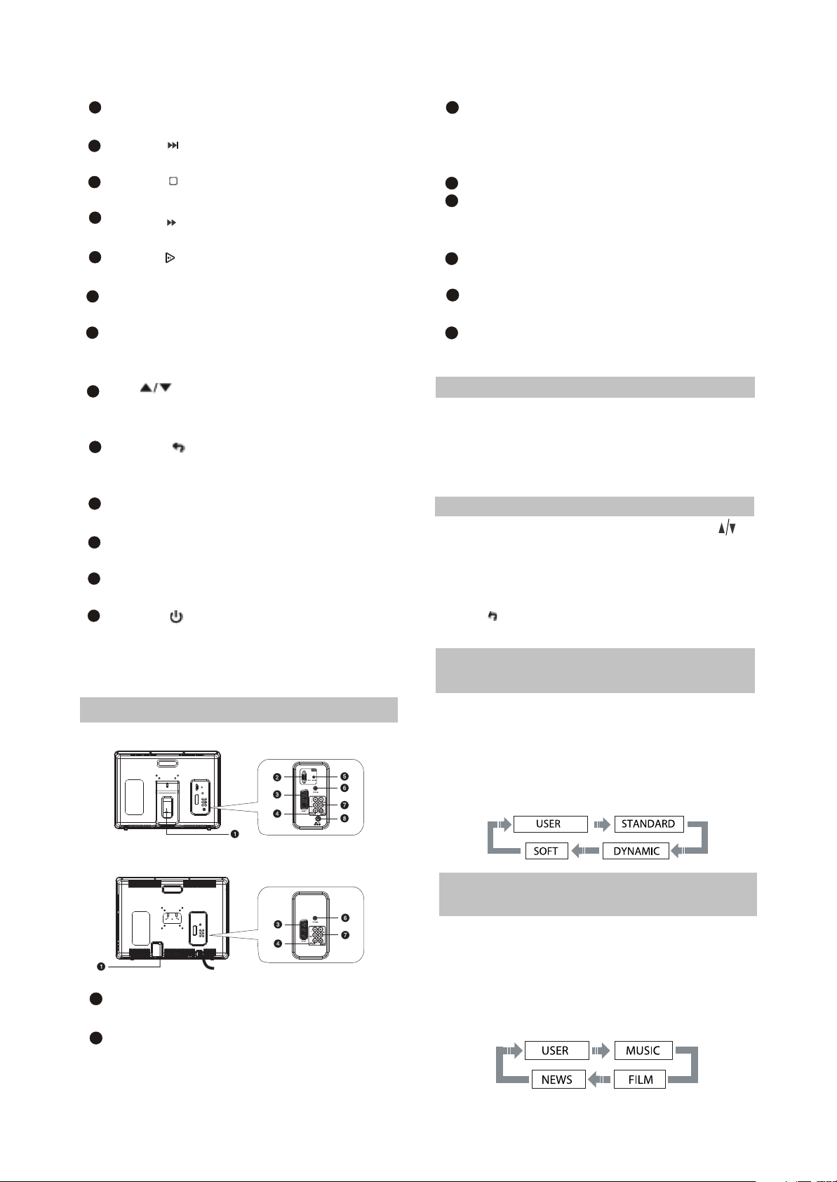
2.1.3 CONTROLS AND FUNCTIONS
(1) Panel controls and indication
1pcs
1pcs
2pcs
1pcs
1pcs
1pcs
1pcs
2pcs
2pcs
1pcs
1pcs
1pcs
1pcs
4pcs
4pcs
4pcs
1pcs
1pcs
For LD1506X
For LD1906X and LD2006X
Front panel(Panel controls and
indication depend on a model of LCD TV.)
Left panel
SETUP button
1
Press to switch to setup mode
2
_VOL+button
Press to adjust the volume.
- 5 -
_CH+button
3
Press to switch between channels/to
choose menu item.
4
SOURCE button
Press to choose the playback mode.
Page 9

STANDBY button
5
Press to switch on the device/into
standby mode.
6
POWER button
Turn on/off the power.
7
Headphones output
Microphone input 1
8
Microphone input 2
9
Front panel
Remote control sensor
10
Power supply indicator
11
(2) Remote control general view
Right panel
12
Disc tray
13
USB port
14
EJECT button
Press to open/close the disc tray.
15
STOP button
Press to stop the playback.
16
PLAY/PAUSE button
Press to playback/pause.
1
EJECT button
Press to open/close the disc tray.
2
LANG button
Press to change language.
3
DISP button
Press to display the disc information.
NICAM button
4
Press to choose audio mode.
5
Numeric buttons
6
BROWSE button
Press to turn on/off the browser function.
CURSOR buttons (UP/ DOWN/ LEFT
7
/RIGHT)
OK button
8
9
SETUP button
Press to switch to setup mode.
10
Button
Press to turn on/off the “Virtual Keyboard”
function.
11
SOURCE button
Press to change the TV /DVD /AV/ SCART/
YPBPR /VGA/ mode.
12
Button
Press to start rewind/rewind scanning.
13
Button
Press to skip backward.
14
REPEAT button
Press to repeat.
15
A-B button
Press to repeat the selected section.
16
Button
Press to turn on/off the sound.
17
VOLUME+/-button
Press to adjust the volume.
- 6 -
Page 10
18
USB/DVD button
Press to select USB/DVD mode.
19
Button
Press to skip forward.
20
Button
Press to stop the playback.
21
Button
Press to forward scanning.
22
Button
Press to playback/pause.
23
ZOOM+/-button
Press to zoom in/out.
24
CANCEL button
Press to go one level back/cancel current
operation.
25
CH button
Press to switch between channels /to
choose menu item.
26
MENU / button
DVD disk menu/PBC function/Press to
return to the previous channel.
27
Q-PLAY button
Press to turn the Q-PLAY mode on.
28
KARAOKE button
Press to change the subtitles language.
29
SUBT button
Press to change the subtitles language.
30
Button
Press to switch on the device/into standby
mode.
2.1.4 CONNECTION AND STARTING
SELECT RETURN
ENTER
SETUP
(1 )Switching interfaces
For LD1506X and LD1906X
3
SCART socket
Meant for external audio video signal
source connection. There is no need to
use additional audiocord.
Y Cb(Pb) Cr(Pr)
4
5
PC AUDIO IN
Meant for PC stereo audio output
connection.
COAXIAL OUT
6
Meant for multi-channel sound playback.
7
AUDIO VIDEO IN
Used for external signal source connection.
12 V socket
8
Meant for adapter connection.
2.1.5
TV MODE
This LCD TV can store up to 100 channels
and enables to scan channels thought automatic,
manual and fine tuning scanning mode. Built-in
TV tuner supports stereo audio playback in
NICAM system.
(1) Adjusted channels selection
#Press +CH-buttons on the left panel or CH
buttons on the remote control each time, when
you want to change a channel.
#Use numeric buttons to enter the number of the
channel.
#Press button to return to the previous
channel.
(2) Default picture settings
selection
#You may select one of the default picture
settings:
USER, STANDARD, DYNAMIC and SOFT.
#You may adjust necessary parameters in the
device menu.
#Turn to Picture item on this page for details.
For LD2006X
1
RF input
Meant for antenna connection.
2
VGA port
Meant for PC connection.
(3) Default sound settings
selection
#You may select one of the default sound
settings:
USER, MUSIC, FILM and NEWS.
#You may adjust necessary parameters in the
device menu.
#Turn to page.13 for details.
- 7 -
Page 11

(4 )Accompanying sound type
#Only some of the TV channels have stereo
accompanying sound in NICAM system.
#Press NICAM button to select accompanying
sound.
(5 ) TV settings
#Press SETUP button to display the menu.
#Use cursor buttons on the remote control or
+CH-buttons on the left panel to select the
item. Use buttons to adjust selected
parameter. Use OK button for confirmation.
Press SETUP button again to return to the
main menu or to exit TV SETUP.
(6) Picture
#Select PICTURE item to adjust picture
parameters.
#You may adjust BRIGHTNESS, CONTRAST,
SATURATION, TINT, SHARPNESS and
COLOR TEMP.
(8) TV setup
Select TV SETUP item to adjust channels.
CHANNEL, COLOR SYSTEM, SOUND
SYSTEM, FINE TUNING, AUTO SEARCH,
MANUAL SEARCH and CHANNEL EDIT.
#CHANNEL item enables to select the number of
adjustable channel.
#CHANNEL EDIT submenu enables to select,
skip and swap the channel.
RETURN
SETUP
#CHANNEL parameter enables to select current
channel.
#SKIP function enables to make current channel
inaccessible while using +CH-button to browse
channels.
NOTE
You can’t adjust TINT while watching TV
channels.
(7) Sound
#Select SOUND item to adjust sound
parameters.
#You may adjust BALANCE, BASS, TREBLE
and NICAM.
ATTENTION! We recommend watching TV at
halfof maximum level of the sound. Continuous
listening at higher level may lead to hearing
reduction.
#SWAP function enables to select the channel
number to swap with current channel.
#SAVE parameter enables to confirm the swap
function.
#FINE TUNING item enables to adjust the
channel frequency accurately.
#MANUAL SEARCH item enables to change
channel settings.
#AUTO SEARCH item enables to adjust channel
setting automatically.
#COLOR SYSTEM item can be changed
between: AUTO, PAL and SECAM. We
recommend to set this item to AUTO.
#SOUND SYSTEM item can be changed
between: B/G, D/K, Land I.
- 8 -
Page 12

(9) Function
You may select LANGUAGE,
TRANSPARENCY, SLEEP and RATIO.
#LANGUAGE item enables to select the OSD
language.
#TRANSPARENCY item enables to adjust
transparency of OSD.
#SLEEP item enables to set the sleep timer.
#RATIO(only for LD1906X)item can be changed
between 16:9 and 4:3.
#RESET item enables to reset all values to
default.
(2)Sound
Select SOUND item to adjust sound
parameters.
You may adjust BALANCE, BASS, TREBLE
and NICAM.
(10) Video settings
#Press SETUP button to display the menu.
#In external video signal playback mode the
menu is the same as the menu, described on
pages 12and 13.
NOTE
In external video signal playback mode TV
SETUP item is inaccessible.
2.1.6 PC MONITOR MODE
(only for LD1506X and LD1906X.)
(1)Picture
Select PICTURE item to adjust picture
parameters.
You may adjust BRIGHTNESS, CONTRAST,
COLOR TEMPERARURE and AUTO CONFIG.
#Select COLOR TEMPERATURE subment to
adjust color temperature of the picture.
#COLOR TEMP. Item can be set to :USER,
NORMAL, WARM and COOL.
#RED, GREEN and BLUE items enables to
adjust RGB value of color temperature.
#Use AUTOCONFIG to configure display
parameters automatically.
NOTE:
The picture can be displayed incorrectly
while adjusting.
(3)Monitor setup
Select MONITOR item to adjust such
parameters as PHASE, FREQUENCY, HPOSITION and V-POSITION.
(4)Function
You may select LANGUAGE,
TRANSPARENCY, SLEEP and RADIO.
#LANGUAGE item enables to select the OSD
language.
#TRANSPARENCY item enables to adjust
transparency of OSD.
#SLEEP item enables to set the sleep timer.
#RATIO(only for LD1906X) item can be changed
between 16:9 and 4:3.
#RESET item enables to reset all values to
defaule except ratio function.
- 9 -
Page 13

2.2 Section Two DVD SEGMENT
2.2.1 Controls and functions
Front panel controls
For LD1506X
For LD1906X and LD2006X
USB port
EJECT button
Press to open/close the disc tray.
STOP button
Press to stop the playback.
PLAY/PAUSE button
Press to playback/pause.
Disc tray
Two USB ports
Disc tray
EJECT button
Press to open/close the disc tray.
STOP button
Press to stop the playback.
PLAY/PAUSE button
Press to playback/pause.
Note:
This model does not support the 8cm disc. Do not insert that type of disc into this device to avoid disc
jam.
2.2.2 FUNCTION SETTINGS
(1) Function selection and change
#Press the SETUP key to show the setup menu. You will see the following image on the screen, as show
on the figure:
#Select the desired menu item using the UP/DOWN buttons button; press the OK key for confirmation.
1.For example, if you wish to change the image settings, you have to select the image item and press
the OK or RIGHT key.
Language
Image
Sound
Playback
Karaoke
Preference
Parental control
Initial help
Reset settings
Exit
Setup menu
DVD menu
Sound track
Subtitle
Mp4 Subtitles
4:3
Off.
+48
+48
AUTO
PAL
NTSC
M.
0
0
TV system
TV format
Off
- 10 -
Sharpness
Gamma
Brightness
Contrast
Hue
Saturation
AUTO
Page 14

2.Using the UP/DOWN buttons, select the
desired item and press OK or RIGHT button.
For example, select the Sharpness item.
Settings will appear on the screen. Then select
the desired sharpness level and press OK for
confirmation.
TV system
TV format
Sharpness
Gamma
Brightness
Contrast
Hue
Saturation
AUTO
4:3
Off.
+48
+48
High
L.
Medium
Low
0
0
3. Press LEFT for exit to previous menu level.
4. Press SETUP to exit setup menu.
(2) Language settings
1. Setup menu: interface language set-up
#Options: Russian, English, Ukrainian,
Romanian.
#Default option: English.
Setup menu
DVD menu
Soundtrack
Sbutitles Off
English
#If the language you selected is not recorded on
the DVD disc, another available language will
be displayed.
5.MP4 Subtitles: selection of subtitles language
#Options: Russian, English, Ukrainian and
Romanian.
#Default option: English.
(3) Image settings menu
1. TV system: TV system selection
#Options: Auto, PAL, NTSC.
#Default option: PAL.
2.TV Format: image ratio settings
#Options: 4:3 pan& scan, 16:9 letterbox and 16:9
TV,4:3 LB.
#Default option: 4:3 LB.
#Some discs are recorded with support of only
one ratio. The selected ratio must comply with
the TV screen.
TV system
TV format
Sharpness
Gamma
Brightness
Contrast
Hue
Saturation
Auto
4:3 LB
Off.
AUTO
PAL
NTSC
L.
0
0
0
0
2.DVD menu: selection of disc menu language
3. Sound: selection of translation language
#Disc menu/translation language options:
Russian, English, Estonian, Lithuanian, Kazakh,
Romanian, Belarusian, Ukrainian, Chinese,
Others.
#Default menu/translation language option:
English.
#Selection of other languages: select the
OTHERS item using the wheel and press OK.
Enter the language code using the numeric
buttons and press OK.
#If the language you selected is not recorded on
the DVD disc, another available language will
be used.
4. Subtitles: selection of subtitles language
#Options: Off, Russian, English, Estonian,
Lithuanian, Kazakh, Romanian, Belarusian,
Ukrainian, and Chinese.
#Default option: off.
#Selection of other languages: select the
OTHERS item using the wheel and press OK.
Enter the language code using numeric buttons
and press OK.
3.Sharpness: image sharpness adjustment
#Options: High, Middle, Low.
#Default option: Middle.
4. Gamma: adjustment of image color
temperature
#Options: High, Middle, Low, Off.
#Default option: Off.
5.Brightness: adjustment of image
brightness
6.contrast: adjustment of image contrast
7.Hues: adjustment of image hues
8.Saturation: adjustment of image saturation
Adjustment of image brightness, contrast,
hues and saturation:
#Select the desired item of the image adjustment
section using the UP/DOWN buttons. Press OK
or RIGHT key to start adjusting the relevant
option.
#Change the option value using the wheel.
#Upon completion press the LEFT button of the
UP/DOWN buttons to return to image setup
menu.
(4) Sound settings menu
- 11 -
Page 15

1.Digital audio output
a).SPDIF format: set-up of digital audio
output options.
#Options: RAW, PCM.
#Default options: RAW.
#When you select the RAW option, the not
decoded signal is transferred to the LCD Tv’s
digital outputs, the decoded signal is
transferred to analog outputs. Decoding is
performed by the built-in decoder of the LCD TV.
This feature is meant to ensure that signal
decoding at digital outputs is performed by an
external device(e.g.an amplifier).
#If you select the PCM option, a PCM coded
signal will be transferred to the LCD Tv’s digital
outputs.
Digital output
Tuning
SPDIF format
LPCM
RAW
48kHz
B)LPCM:set-up of digital audio output
options to comply with different amplifiers
and receivers.
#Options: 48kHz 16 bit, 96 KHz 24 bit,192kHz 24
bit.
#Default option: 48kHz 16 bit.
2. Sound correction
A)Equalizer: equalizer modes
#Options: Off, rock, pop, live dance music,
Techno classics, soft .
#Default option: off.
B)Echo: echo effects
#Options: Off, concert, living room, hall,
Bathroom, cave, arena, church.
#Default option: off.
C)Tone balance: adjustment of tone balance
level.
#Adjust the tone balance level using the cursor
buttons.
#Press the LEFT button to return to sound
correction set-up menu.
(5) Playback settings
1. DVD
Advertisement skip: skip the unskippable
block while playing a DVD disc.
#Options: Yes, No.
#Default option: number
2. VCD/SVCD
PBS menu: PBC menu on/off
#Options: On, Off.
#Default option: On.
#If On option is set, while reproducing discs, a
menu will appear, in which you can select the
order of playing the disc content. If the Off
option is set, the reproducing of content is
performed in the order, in which it is recorded
DVD
VCD/SVCD
Files
Repeat
All types
Advertisemenu No
off
3.Files: selection of reproduced files on the
disc
#Options: Audio, Pictures, Video, All types.
#Default option: All types.
4.Repeat: file repeat mode
#Options: Off, Single, All.
#Default option: Off.
(6) Karaoke settings menu
1.Microphone: microphone on/off
#Options: On, Off.
#Default option: On.
2.Kar.help: karaoke -disc playback mode
#Options: L Channel, R Channel, No ast, No voc.
#Default option: No voc assist.
Microphone
Kar.Help
Volume
Echo
No ast.
3.Volume:
Microphone: microphone sound volume level
#Using the UP/DOWN buttons adjust the
microphone volume level.
#Press LEFT key of the UP/DOWN buttons to
return to karaoke settings menu.
4.Echo:echo level while playing the karaokedisc
#Adjust the echo level Using the UP/DOWN
buttons.
#Press LEFT key of the UP/DOWN buttons to
return to karaoke settings menu.
On
On
Off
5
5
- 12 -
Page 16

Sign of trouble Cause of trouble Act ions t o ellminate the t rouble
No sound
1.Poor audio cable c onnect ion.
2.Dis c dirt y or damaged.
3.Sound disabled by the MUTE
button.
1.Mak e proper connect ion.
2.Clean the disc .
3.Pres s t he MUTE button.
(7) Preference settings
1.Screensaver: screen saver on/off
#Options: On, Off.
#Default option: On.
2.Gr.equalizer: spectrum analyzer
#Options: On, Off.
#Default option: Off.
Screen saver
Gr.equalizer
On
Off
On
Off
(9) Initial setup menu
#Press the RIGHT key to enter the initial settings
menu, then select the desired item using the
cursor buttons and press OK key for
confirmation.
#While being in this menu section, you cannot
return to the previous level by pressing the
Auto
PAL
NTSC
(8) Parental control settings
1.Category: set-up of age restrictions to
prevent children from seeing undesirable
discs.
#Options: Any, Kid, G,PG, PG-13, PGR, R, NC-
17.
Allowed..
Set password
2.Change password: set-up of a four-digit
password to change the level of age
restrictions.
#Default option: 7890
Old password
New password
Verify
OK
Any
any
Kid
G
PG
PG-13
PGR
R
NC-17
Cancel
(10) Reset settings to default
#Resetting all settings and restoring default
options, except age restrictions level and
Password.
Load factory settings
OK Cancel
(10) Exit settings menu
#Select the exit item using the UP/DOWN
buttons and press the OK key to exit the menu.
Language
Image
Sound
Playback
Preference
Parental control
Initial setup
Reset to defaults
Exit
2.2.3 OTHERS
(1) Useful notes
#To extend the service life of your LCD TV make pauses of not less than 30 seconds between switching
off and repeatedly switching on the LCD TV.
#Disconnect the LCD TV from the wall outlet after shutdown.
#Some LCD TV’S functions may not be applied to some discs.
#Use supply sources of rated voltage, otherwise the LCD TV may not function or be damaged.
#In case of the LCD TV’s occasional stops, please switch the power supply off and then on again.
(2)Trouble shooting
Please check probable causes of malfunction before addressing the service center.
- 13 -
Page 17

No image
1.Poor video cable c onnect ion.
2.Incorrect setti ngs of your TV
set.
3.The TV is in t he progressi ve
scan mode while y our TV set
does not support t his m ode.
1.Mak e proper connect ion.
2.Correct the s etti ngs of your TV s et.
3.Place the TV in the int erlaced s can mode
through the TV's menu.
Blac k and whit e image
1.inc orrect TV c olor sy stem
selec ted.
2.Color level on the TV set
adjust ed incorrec tly .
1.Set the appropriat e color s ys tem via the
menu: S ETUP>Image> TV scan.
2.Readjust the c olor sy st em of your TV set .
Disc s c annot be read
1.Disc not insert ed.
2.Disc ins erted inc orrectly.
3.Condensat e on the DVD
player's laser head.
1.Insert the dis c.
2.Inst all the di sc with t he label s ide facing up.
3.Switch the TV on without disc for an hour.
Microphone does not
operate
1.Microphone is unplugged.
2.Low level of the mic rophone's
sound volume.
1.Connect the mi crophone.
2.Adjust the level of the mic rophone's sound
volume.
Remote c ontrol does not
operate
1.Remote control is i ncorrect ly
direct ed at the TV's sc reen.
2.Distanc e to the TV i s in
excess of 8 meters.
3.Run out bat teries .
1.Use t he remote c ontrol ac cording t o the
manual.
2.Decreas e the dis tanc e to the TV.
3.Replace both batt eries.
some functions do not
work
1.Disc is recorded inc orrectly.
2.Incorrect key s equence.
3.St atic voltage on the housi ng.
1.W ait5-10 s econds and the device will
automat ical ly t eturn to norm al st ate.
2.Repeat t he operation one more t ime.
3.Switch the device off for 1-2 minutes and t hen
switch it on again.
Unstable image or
abnormal pic ture col or
1.Incorrect TV set set ting.
2.There is s omethi ng wrong with
the data i n the E P ROM.
1.Correct the TV set set tings . 2.Res et the TV
set to default s etti ng.
LD1506X LD1906X LD2006X
Type
class
Size(")
Height(mm)
Widt h(mm)
Dot Pitch(H mm × V mm)
Viewing A ngle(H)
15
228.19
304.13
0.297×0. 297
120
19
256.5
410.4
0.285×0. 285
170
20
306
408
0,637×0, 637
140
Frequency
Verti cal(Hz )
Horizont al(kHz )
Display color
TFT,colored
ll(ISO 13406-2)
Display
50-75
30-75
16 700 000
(3)Technical characteristics
- 14 -
Page 18

Maximum Dis play
Mode
Resolut ion
Verti cal frequenc y(Hz)
1024×768
75
1440×900
75
640×480
75
Inputs
Video
Composit e
Component
VGA
RGB/SCART
Audio
Stereo
PC audio
Others
Karaoke
USB
RF
Audio out puts
Headphone
Digital coax ial
1
1
1
1
1
1
Color system
TV tuner
Video inputs
Sound sy st em
TV tuner
Disc types
Formats
-
Power supply
Power Consumpt ion
(Maximum)(w)
Power Consumpt ion
(Power Saving)(w)
Environmental
considerati on
Operating t emperature(°, C)
Operating humidit y(%)
Stori ng temperat ure (°,C)
Stori ng humidit y(%)
Dimensi ons(mm )
438.7×295. 7×73.4 498×370.6× 82.5 620×450×202
Weight
Net weight(kg) 6.5 6.9 7.9
+5 +35
10-80
-20 +45
5-95
CD-R/RW ,DV D-R/RW ,DV D+R/ RW
DK,I,BG,L
PAL,SECAM
PAL, SECAM, NTSC 3.58, NTSC 4.43,PAL60
Built-in DVD player
DVD-V ideo, DivX,XviD,SV CD,V CD,CDDA, HDCD,M P3, WM A,Kodak Pic ture CD,JPEG
~100-240,50/ 60
Volt age and frequency(V ,Hz)
Volt age of external (V,A )
Power adapter
1
1
1
1
2
1
1
1
1
1
1
1
-
1
2
2
1
= : + 12
54
<3
2
2
1
= : + 12
2
2
1
65
<3
#We are permanently improving the quality of our products; hence the product’s design, functionality
and technical characteristics may be modified without prior notice.
#We do not guarantee that all discs can be played smoothly due to the disc quality, disc recording
quality and recording format.
- 15 -
Page 19

Chapter Three Principle and Servicing
The previous manual: TV part
Section One Principle of the player
3.1.1 System control principle
System control schematic diagram is shown in the figure 3.1.1.1:
Key-press board
Reset circuit
Remote control board
MT1389HD
Mute control circuit
FSAV433
KEY1~KEY5
RESET
IR
DVSTB
DVSCK
DVSDA
MUTE
ONMUTE
VS1
VS2
U104
PS25LV010
I
Z
O
ID
IC
D
P
I
S
SP
SP
K
PIC
WP
S
SCART JACK
S
B
F
S
U101
IC-MST718MCU
T4094
Serial/parallel converter
VSDA
U102
CD4094
VSCK
X
T
L
C
S
RX
SDA
INVERTER
ON/OFF
PANEL_ON
FCLK
FDATA
FCS
ASW
8216_RST
STBY
FMUTE
Inverter components
Emitting module of RF
BH1418
PANEL_ON
control circuit
DVB Moduie
STV8317
power control circuit
BH1418
Figure 3.1.1.1 System control schematic diagram
- 16 -
Page 20

3.1.2 OVERALL WIRING DIAGRAM
PANEL
1234567891011
SVA150XG04TB 15 TFT
12131415161718192021222324252627282930
1210312
EARPHONE&MIC
PHONE BOARD
61506-2
4941427
CN102
CN701
INVERTER BOARD
DVD LOARD
5INV203-3
5462768
DVD-PICK UP
TD-S208-62(HD62 PICKUP)2#
2380286
GND
+12V
+12V
Brightness
GND
BLON
GND
GND
LD-DVD
NC
+5V
MDI
LD-CD
VRDVD
VRCD
NC
E
+5V
V20
GND
F
B
A
RFO
IOA
D
C
TKTK+
FC+
FC-
SL-
SL+
LIMIT
GND
SP+
SP-
TROUT
DISCEJT
GND
+5V
TRIN
GND
+5V
CN101 CN103
CN107
CN108
CN119
J501
AMPRIN+
GND
ARPLIN-
GND
AMPROUT+
GND
DET#
OKA
GND
VCC-PANEL
VCC-PANEL
VCC-PANEL
LVA3 P
LVA3 M
GND
LVACKP
GND
GND
GND
LVACKM
LVA2 P
LVA1 P
LVA2 M
LVA0 P
LVA1 M
GND
LVA0 M
GND
LVA3 P
LVA3 M
LVBCKP
LVB2P
LVBCKM
LVB2M
LVB1P
GND
LVB1M
LVB0P
LVB0M
CN111
+12V
CN2
AMPROUT-
CN113
MAIN BOARD
21901-2
4941425
CN110
CN102
CN105
CN104
CN106
LD1506X
Block diagram
for machine
12VSW
CH
IT
#
0
1
D
GND
D
S
M
MS
SW
D2#
MS
LK
SC
ND
SB_
MSD3#
G
SDCLK
U
M
5449509
@5AK0833-10
POWER ADAPTER
S
S
MD
B
C
ND
G
MS
SD
CRAD&USB
0
D
D
D1
D2
N
D
GND
MSIN
SDCD
G
S
5449476
D1903-3
BM
ND
D
D
S
S
SDD3
G
US
GND
Dv33
GND
USBP
BOARD
5VEXT
GND
STBY
IR
+5V
+5V
REMOTE BOARD
KEY1
B1506-0
5449978
DVD KEY BOARD
SW1
GND
KEY2
GND
J1903-0
SW2
41903-0
5449477
5449438
TV KEY BOARD
figure 3.1.2.1 overall wiring diagram
- 17 -
Page 21
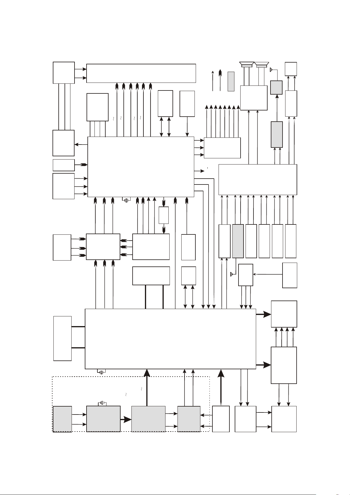
3.1.3 Block diagram of the player
BOARD
INVERTER
U104 FLASH
BLON
Brigtness
+12V
PS25LV010
LVA0 P LVA3P
SPICZ
SPIDI
SPICK
SPIDO
INVERTER_ON/OFF
Control circuit
of boost
voltageboard
VGA
JACK
IR
KEY1
KEY2
Button board
& receiving
board of RC
7/8
9/10
12/13
Y
PBIN
PRIN
EPR
EPB
U106
EY
FSAV433
Video
electronic
switch
YPBPR
INPUT
JACK J105
PANEL
U103
LVBCKP LVBCKM
LVB0P L VB3P
LVA0 M LVA3M
U101
X101
LVB0M L VB3M
LVACKP LVACKM
MST718
LCD picture
processor&MCU
67
24
25
66
12MHZ
SDARX
Video
SCLTX
SCVBS+
SCVBS-
SCART
JACK
SR SGSB
SCART
RF_OUT
1
2
14
NC
VIDEO
AUDIO
21901-2
24C32
EEPROM
Reset circuit
Q103 Ce101
STBY1
8216_RST
FMUTE
ASW
ONMUTE
VS1
MUTE
MST_RESET
3
VSCK
2
VSDA
T4094
74
U102
1
PANEL ON
VS2
CD4094
83
73
34
amplify
30/31
22/23
63
FMR
DRIN
FML
DLIN
TV+/TV-
24
23
U117
DVSCK
DVSDA
DVSTB
U114
TUNER
U113
TEA5764
MC4580Audio
amplifying circuit
15
RF
Amplify
U112
Audio
amplify
TDA7266
4
12
Audio output
amplifying
RF_OUTPUT
LSL
LSR
BU1418
FLIN
circuit
FM Modulate
AO2L
AO2R
FRIN
U4
STV8317
NICAM
processing
circuit
AVRIN
PCLIN
PCRIN
J103
PC AUDIO
SRIN
SIOMAD
MONOIN
U114
TUNER
AVLIN
SLIN
J105
SCART JACK
A/V input terminal
DCVBSIN+/DCVBS-
U303
U301
SDRAM
DY
DPB
DPR
DDQ[0:15]
U302
DVD
FLASH
U115
DMA[0:11]
Mt1389
24C16
EEPROM
DSDA
DSCL
89AL
226
100
98
109
U5
CS5340A/D
89AR
Convertion
ABCK
ALRCK
AMDATA
224
OKA
MIC
BOARD
61506-2
DVD
PICK_UP
A/B/C
D/E/F
FC-
FC+
TK+
TK-
DFA[0:20] DFD[0:7]
X109
DVB Part
If1
If2
TUNER
U119
27MHZ
X602
20.48MHZ
PN2020
XIDD0 XIDD15
TSDATA0 TSDATA7
U116
MT8606
DVD decode chip
GPIO_4
GPIO_3
XIDD0
XIDD8
DVB/CARD
Conversion
MSD1
MSD0
CRAD
switch
U108/U2
BOARD
54
39
FOSO
TRSO
FMSO
TROPEN
TRCLOSE
U118
BA5954
Servo driving
DMSO
SL+
SL-
LOAD+
Tray
LOAD-
open/close
circuit
DVDLOAD
figure 3.1.3.1 Block diagram of the player
- 18 -
Page 22

3.1.4 Audio circuit
Audio processing circuit is mainly responsible for the switch, amplifying and restire of audio and
composed of audio source input selection and NICAM processing circuit, audio amplifying circuit and
mute control circuit. Audio processing circuit block diagram is shown in the figure 3.1.4.1:
MT1389
ALRCK
ABCK
AMDATA
U5
CS5340A/D
conversion
OKA
MIC
BOARD
61506-2
89AL
226
89AR
224
PC AUDIO
J103
U114
TUNER
SCART JACK
J105
A/V input terminal
U117
MC4580Audio
amplify circuit
Figure 3.1.4.1 Audio processing circuit block diagram
DLIN
DRIN
PCLIN
PCRIN
SIOMAD
MONOIN
SLIN
SRIN
AVLIN
AVRIN
28
29
13
U4
14
STV8317
NICAM
92
98
processing
circuit
9
10
19
20
34
36
17
18
LSL
LSR
AO2L
AO2R
U112
4
TDA7266
Audio
12
amplifying
Audio output
Amplifying
circuit
1
2
15
14
3.1.5 Power circuit
Power circuit supplies stable and pure power for each unit circuit to ensure normal working of the
player. Power circuit block diagram is shown in the figure 3.1.5.1:
AMPRIN+
AMPLIN+
AMPROUT+
SCART
61506-2
AMPLOUT+
IC 503
AP1506
U511
+12V
Power adapter
Standby
control circuit
AP1506
U506
INVERTER
BOARD
U502
Si9435
Figure 3.1.5.1 Power circuit block diagram
+5VEXT
+12V
STBY
5V
- 19 -
U505
AMS1117
U507
Lm1085
MST718
U513
U1
AMS1117
U521
Lm1085
IC702
AZ1084-ADJ
3.3V
+2.5V
MST718
+3.3V
1.8V
Dv33
FOR PANEL
Page 23

3.1.6 Video circuit
Video circuit is mainly responsible for the input of external video signals, the processing of video
signals send from tuner, and the drive processing of LCD screen, including video input selection, video
A/D conversion circuit, LCD picture processing circuit and video output circuit. Video circuit block
diagram is shown in the figure 3.1.6.1:
Y PB PR
INPUT
JACK
185
183
182
Mt1389
187
EY
EPB
EPR
Video
DY
Electronic
switch
DPB
DPR
FSAV433
SR
DCVBSIN+/DCVBS-
U106
SG
SB
SCART
JACK
13
15
17
PRIN
PBIN
Y
X101
12MHZ
SCVBS+
SCVBS-
SCLTX
SDARX
Video
amplifying
7/8
9/10
12/13
U101
MST718LCD picture
processor&MCU
24
25
67
66
34
22/23
30/31
LVA0~3P
LVA0~3M
LVB0~3P
LVB0~3M
LVACKP
LVACKM
LVBCKP
LVBCKM
BIN+ BIN-
GIN+ GIN-
RIN+ RIN-
VGA-VSYN
VGA-HSYN
TV+/TV-
PANEL
VGA JACK
TUNER
Figure 3.1.6.1 Video circuit block diagram
- 20 -
Page 24

Section Two Troubleshooting flow chart
[ Flow chart 1 ] Trouble symptom: standby light is not on
Trouble description: connect with power, standby indicator light is not on, machine has no response
and buttons have no function.
Machine not power on
Whether
12V voltage
outputted by power
adapter is
normal
Y
Check
whether J501 pin 2
12Vvoltage is
normal
Y
Check
whether U503 pin 2
5V voltage is
normal
Y
Check
the power supply
loop from +5VEXT power
toMST718 is
normal
Y
Check
whether standby
control signal outputted
by MST718_57 is
normal
N
Check power adapter
N
Check flat cable from power
adapter to video main board
N
N
N
Change U503
Check power supply loop
Check
whether reset
signal of MST718
is normal
N
Check reset system circuit
Y
Check
whether Q117 is
normal
Y
Check the standby indication
circuit on subsidiary board
Y
Check
whether X101 clock
signal is normal
Y
Change MST718
- 21 -
N
Check clock system circuit
Page 25

[ Flow chart 2 ] Symptom: power not on
Trouble description: test after machine power on, standby indicator light is not on and +12V power
outputted by power adapter is abnormal.
Power not on
Check fuse, TC1 and
rectifying bridge
Check NCP1207 and
peripheral elements
Change Q1
Check
whether power
board Cn2
has 12V voltage
Y
Check according to
troubleshooting process
for“player not switch on”
N
Check
whether power
board TC1 has 310v
voltage
Y
N
Check
whether each pin
voltage of U1 is
normal
Y
N
Check
whether Q1 is
damaged
Y
N
Check
whether 12v
resistor to ground
is normal
Check whether filtering
N
capacitor TC3/TC4 has
electric leakage and
short-circuit
Y
N
Check
whether VD4
has secondary
voltage
Y
Check
whether VD4
secondary voltage is
normal
N
Check feedback loop
U2/U3
Y
Check
whether voltage
of TC2 two ends
is normal
N
Change L3
Y
Change transformer
N
whether transformer
is normal
Check VD4
Check
END
Y
- 22 -
Page 26
[ Flow chart 3 ] Symptom: no sound
Description: there is image, but no audio output.
All input source has
no sound output
Y
Check
whether pin 34/36
of STV_8317 has signal
output
Y
Check
whether power
supply of power amplifier
board TDA7266 is
normal
N
N
Check STV8317 and
peripheral elements
Check power supply loop
of TDA7266
Y
Check
whether TDA7266_6
pin is high level
Y
Check
whether audio output
pin waveform of
TDA7266P is
normal
Y
Check speaker and line
N
Check mute control circuit
N
Change TDA7266P
- 23 -
Page 27

[ Flow chart 4 ] Symptom: white screen
Description: screen is white and indicator on.
White screen
Check
whether u502_D
voltage is normal
Y
Check
whether 2.5V
voltage of pin 2 of
U507 is normal
Y
Check
whether 3.3V
voltage outputted
by U505 is
normal
Y
Check
whether X101 clock
is normal
Y
N
whether u502_G pin is
low level
Change U502
N
N
Change U507
Change U505
N
Check X101/C103/C104
Check
Y
N
Check Q504 and peripheral
elements
Check
whether U15_37
(PANEL_ON) is low
level
Check
whether Q505_C is
high level
N
Change MST718
Y
N
Check Q505 and peripheral
elements
Y
Check
whether drive
output pin MST718
outputs normally
Y
Check
whether the socket
and flat cable from main
board to display screen
are normal
Y
Change display screen
N
Change MST718
N
Change flat cable or socket
- 24 -
Page 28

[ Flow chart 5 ] Symptom: DVD has no sound
Trouble description: when machine is set in DVD state, there is image but no sound. External input
and TV sound are normal.
In DVD state, playing is normal
and there is no sound output
Y
Check elements between
CE167/CE163 and U117
Check A12V power supply
loop
Check MT1389
N
N
N
N
Check
whether pin 2/6
signal input of U117
is normal
Check
pin 8 power supply of
U117 is normal
Change U117
N
Check
whether CE167/CE163
has audio signal
Y
N
Y
Y
Y
Y
Check
whether pin 1/7 of
U117 has audio signal
output
Y
Check
whether secondary
of TC166/CE165 has
audio signal
output
Y
Check
whether pin 28/29
audio input of U4 is
normal
N
N
Check mute circuit
Check the line between
U4
Y
Change STV8317
- 25 -
Page 29

[ Flow chart 6 ] Symptom: black screen
Trouble description: after power on, screen has no display and backlight cannot be on.
Black screen
After
power on, whether
indicator circuit working
is normal
Y
Check
whether CN103 pin 6
power supply is
normal
Y
Check
whether CN103_3 is
high level
Y
Check
whether boost
board has high
voltage output
Check according to
N
troubleshooting flow of
“Machine cannot power on”
N
Check 12V power supply
loop
N
N
Change Q102
Check boost board
Y
Change display screen
- 26 -
Page 30
[ Flow chart 7 ] Symptom: DVD has no image
Description: DVD has no image but has sound.
DVD has no image
Y
Whether
machine switches in
DVD state
Y
Check
whether L195/L196/L198
has video signal
output
Y
Check
whether pin 13/15/17
of U106 has signal
output
Y
N
N
N
Change machine setup
Check Mt1389 and
peripheral elements
Check U106 peripheral
elements
Check
whether pin 7/9/12
input signal of MST718
is normal
Y
Change MST718
N
Check components video
input loop
- 27 -
Page 31

[ Flow chart 8 ] Symptom: TV cannot search channels
Description: channel cannot be searched.
T V cannot search channels
Check
whether tuner
has TUNER_CVBS
signal output
Check whether tuner power
N
and TV signal have input
and then change tuner
Y
Check
whether TUNER_CVBS
signal transmits
onto TVP5146
N
Check the path between
tuner to Mst718.
Y
Check SCL and SDA data
pin is normal
[ Flow chart 9 ] symptom: NICAM has no function
Description: NICAM has no function and cannot be realized.
NICAM has no function
Check
whether STV8317SIF
signal is
normal
Y
Check
whether clock frequency
is normal
Y
Change STV8317
N
whether clock frequency
is normal
Check
Y
Check the circuit between
tuner SIF signal and STV8317
N
Check crystal oscillator
resonance circuit
N
Change tuner
- 28 -
Page 32

[ Flow chart 10 ] Symptom: player not power on
Description: switch on power, indicator light is not on and buttons have no function.
Player not power on
Check MST718 and
peripheral elements
Change Q117
N
button, whether 101_57
After
pressing OPEN
is high level
Y
N
Check
whether Q117 is normal
Y
Check standby indication
circuit
pressing POWER
N
button, whether panel
working indicator light
works correctly
Whether U503_1 is
Whether U503_2 is
whether U101 reset
is normal
After
12v
+5V
Check
Y
N
Check 12V power supply
circuit
Y
N
Check U503 and
peripheral elements
Y
N
Check system reset circuit
Y
whether X101 clock
Change(U101)
- 29 -
Check
is normal
Y
MST718
N
Check system clock circuit
Page 33

[ Flow chart 11 ] Symptom: screen image flickers
Description: screen image flickers and sound is normal.
Screen image flickers
Check
whether screen
flickers under other
signal source
Y
Judge
whether it is the
back ground light that
flashes
Y
Change
inverter and check
whether it restores to
be normal
Y
Whether socket has 12v
voltage
N
Check whether software
version is correct
N
Check whether display screen
flat cable contact is good
N
Check whether there is +12v
voltage that outputs to inverter
- 30 -
Page 34

[ Flow chart 12 ] Symptom: colour has distortion
Description: picture colour has distortion.
Colour has distortion
Y
Check
whether the TTL
output signal of
MST718 is
normal
N
Check whether clock
frequency is normal
N
Check X101/C103/C104
Y
Check
whether 3*8bit
digital signal of
Cn1 is normal
Y
Check
whether CN1 has
rosin joint, false welding
and disconnected
pin
Y
Check
whether video flat
cable is disconnected
Y
Check
whether connecting
board has rosin joint and
whether socket has
disconnected
pin
Y
Change MST7118
N
Check the path between
MST718 and Cn1
N
Weld again and change
socket
N
Change video flat cable
N
Change display screen
Y
Check again
- 31 -
Page 35

[ Flow chart 13 ] Symptom: Troubleshooting flow chart of no sound for MIC(check
whether MIC is on before detecting, whether player outputs sound normally).
No sound for MIC
Y
Check
whether pin CN2_2 has
signal input
Y
Check
whether signal of
pin 12 of U5 is
normal
N
Replace flat cable from MIC
board to video main board
N
Check elements from
U4 to CN102
Check
whether pin U44_7
has signal
output
Check
whether CN102_2 has
signal output
CN102
N
Y
Check
whether U44_2 has
signal input
Y
Check
whether U44 power
supply is normal
N
Check MIC socket and
elements from socket to U44
N
Check power supply circuit
Y
Check U44 and
peripheral element
N
Check MIC detecting
circuit
Y
Y
Check
whether signal from
U4 to Mt1389 is
normal
Y
Replace Mt1389
N
Check U5 and its
power supply
- 32 -
Page 36

Section Three Waveform diagram
This section collects signal waveform diagram of audio, video and each unit circuit with the purpose
to help servicing personnel to judge where trouble lies in accurately and quickly to improve servicing
skills. For the difference of oscillograph's type, model and tuner, a certain difference may exist, so the
servicing personnel are expected to pay more attention to check in daily operation.
1. System reset signal waveform diagram: waveform comparison diagram for +5EXT and system
reset pin during the course of power on.
MST RESET
5VEXT
2. U104_2(SO) waveform diagram.
- 33 -
Page 37

3. U104_1 (CE) gating signal waveform diagram.
4. U104_6 (SCK) clock signal input waveform diagram.
5. U104_5 (SI) data input pin waveform diagram.
- 34 -
Page 38

6. MST718 clock signal waveform diagram: waveform diagram when X101 is working (frequency
12MHZ).
7. Q1_C:video signal waveform diagram for pin when machine is receiving Q1_C standard signal
source in TV mode.
8. U103_6: waveform diagram of SCL in IIC bus.
- 35 -
Page 39

9. U103_5:waveform diagram of SDA in IIC bus.
10. TV audio signal waveform diagram: waveform diagram for audio signals outputted by U114_14
pin when machine is receiving standard signal source in TV mode.
11. TV video signal waveform diagram: waveform diagram for video signals outputted by U114_12
pin when machine is receiving standard signal source in TV mode.
- 36 -
Page 40

12. U114_12:waveform diagram for video signals outputted by pin 12 of tuner when machine is
receiving TV signal in TV mode.
13. U114_11:output waveform diagram of NICAM output pin.
14. NICAM processing circuit clock signal waveform diagram: waveform diagram when :X301 is
working (frequency 27MHZ).
- 37 -
Page 41

15. Waveform of clock signal outputted by MST718 in LVDS output mode. MST718_101).
16. Waveform of digital signal outputted by MST718 IN LVDS output mode. MST718_99).
17. 8317_34:waveform diagram after the audio signals from tuner are processed by STV8317 and
then output from pin 34/36when machine is receiving standard signal source in TV mode.
- 38 -
Page 42

18. 8317_28: when machine is in DVD state, audio signals outputted by Mt1389 output from pin
18/19 after being processed by STV8317.
19. PANEL_ON: waveform comparison diagram for STBY and PANEL_ON signal when machine
enters from standby to power-on.
STBY
20. 8317_17: output waveform of standard signal source in TV mode.
- 39 -
Page 43

21. INVERTER:waveform comparison diagram for STBY and ON/OFF_INVERTER signal when
machine enters from standby to power-on.
- 40 -
Page 44

Section Three Servicing and Principle
The next manual: DVD part
Section One Principle of the player
3.1.1 Audio circuit
1. Audio signal process block diagram is shown in the figure 3.1.1.1:
186
184
89AL
89AR
2
U117
6
DLIN
DRIN
TDA
7266P
STV8317
MT1389
SAPDIF
Figure 3.1.1.1 Audio signal flow chart block diagram
Optical
terminal
SOUTL
SOUTR
SCART
3.1.2 Video circuit
1. Video signal flow chart diagram is shown as in the following figure 3.1.2.1 :
YUV6
182
YUV5
183
YUV4
185
MT1389
L196
L195
L198
DPR
DPB
DY
10
U106
6
FSAV433
2
PRIN
PBIN
Y
7
11
9
MST718
187
YUV3
DVCVBSIN+
L197
Figure 3.1.2.1 Video signal flow chart
DVCVBSIN-
- 41 -
Page 45

3.1.3 Servo circuit
1. Servo circuit block diagram is shown as in the following figure 3.1.3.1:
CN101
Main axis electric machine
Main axis control
detect circuit
Switch circuit
APC circuit
A B C D E F RFO
17
18
23
26
FOSO
1
FMSO
TRSO
DMSO
6
SL+
SL-
Disc in/out
circuit
TK-
15
TK+
16
FC+
14
FC-
13
SP-
SP+
Figure 3.1.3.1 Servo circuit block diagram
BA5954
12
11
Feed electric
machine
IOA
MD11
LDO2
LDO2
MT1389
3.1.4 USB/CARD circuit
1. USB/CARD circuit is shown as in the following figure 3.1.4.1:
J902
USB JACK
J901
USB JACK
USBP2
USBM2
USBP1
USBM1
Figure 3.1.4.1 usb/card circuit diagram
U901
ADG713
Add usb switch
- 42 -
USB_SWITCH
USBM
USBP
214
48
47
MT1389
Page 46

3.1.5 Decode circuit
1. Decode circuit block diagram is shown as in the following figure 3.1.5.1:
FLASH
PWR
PRD
PCE
A0~A20
AD0~AD7
URST
Reset
circuit
SDA
SCL
EEPROM
24C02
MT 1389
Clock
27M
SDCLK
SDCKE
DCS
DRAS
SWE
SDRAM
DQM0
DQM1
DQ0~DQ15
MA0~MA11
V1.8
1.8V
voltage
regulating
U509
Figure 3.1.5.1 Decode circuit block diagram
- 43 -
Page 47

Section Two Troubleshooting flow chart
1. Troubleshooting process for ”DVD has no output” is shown in the figure 3.2.1.1:
Trouble description: when switching in DVD state, there is no DVD image and loader has no action
of drawing in disc.
Power on and switch machine
in DVD state, DVD cannot work
and has no power-on image.
Whether
TV function is normal
Y
Check
whether 3.3V
power outputted by U521
and 1.8V power outputted
by U1 are
normal
Y
Check
whether 27M clock is
normal
Y
Check
whether pin 68
reset signal of MST718
is normal
Y
Check
whether SDRAM
and FLASH power supply
is normal
N
Check circuit of TV part
N
Check
whether +5V of
U506_2 is
normal
Check U1/U521 and
peripheral elements
N
Check X109/C398/C399
N
Check system reset circuit
N
Check voltage stabilizing
and filtering circuit of 3.3V
1.8V
N
Check U506/Q3
Y
Y
Upgrade
FLASH and whether
machine is
normal
Y
Check
whether SDRAM clock
is normal
Y
A
N
Change FLASH
N
Check
whether FLSAH
and MT1389 have rosin
welding
Y
Weld again
- 44 -
Page 48

A
Check
whether SDRAM
works
Y
Change Mt1389
Figure 3.2.1.1 Troubleshooting flow chart for “ ”DVD has no output
N
Check
whether SDRAM
Mt1389 has rosin
joint
N
Check SDRAM and MT1389
Y
Weld again
- 45 -
Page 49

2. Troubleshooting process for “Not read disc” is shown in the figure 3.2.2.1:
Trouble description: switch machine in DVD state, load disc and machine displays that there is no
disc or cannot read disc for a long time.
Not read disc
Whether
pick-up resets
Y
Whether
there is focus
action
Y
N
Whether
pin 26 of D5954
has feed signal input
Y
Check
whether voltage
on two ends of electric
machine is equal
Y
Check D5954
N N
Whether
pin 1 of D5954
has focus signal
input
Y
Check
whether pin 13, 14
voltage of D5954 is
normal
Y
N
Check MT1389 and
filtering capacitor
N
Check MT1389 pin
filtering capacitor
N
Check electric machine
Check D5954
Whether
main axis electric
machine rotates
Y
Whether
pick-up emits light
Y
B1
Check the line from
pin 1, 2 of CN101 to coil
N
N
pin 5 of D5954 has
whether pin 11, 12
voltage of D5954 is
Check electric machine
whether APC
circuit supplies voltage
Change loader
Whether
signal input
Y
Check
normal
Y
Check
for pick-up
Y
N
Check MT1389 pin filtering
capacitor
N
Whether D5954
N
Check
whether LDO_DV33
is normal
B2
N
Check power supply circuit
Y
- 46 -
Page 50

B1
Whether
disc rotation speed is
normal
Y
Change loader
N
there is ABCDEF signal
Check MT1389 and its
B2
Check
whether LD-DVD
LD-CD is normal
Y
Whether
there is RF signal
Y
Whether
Y
peripheral
N
Check Mt1389
N
Change loader
N
Check CN101 and flat cable
Check
Q110, Q111
and socket Cn101
N
Change
Y
Change 24P flat cable
Figure 3.2.2.1 Troubleshooting flow chart for “Not read disc”
- 47 -
Page 51

3. Troubleshooting process for “DVD has no video output” is shown in the figure 3.2.3.1:
Trouble description: machine works normally in other state; when switching in DVD state, there is
sound output but no image output.
DVD video has no output
Check
whether video output
mode switch is
correct
Y
Check
whether 27M clock is
normal
Y
Whether
a single video signal
has no output
Y
Whether
components video
output is
normal
Y
Whether
pin 182.183.185
of MT1389 have signal
output
N
Resume set mode
N
Check clock circuit
N
N
Mt1389 whether
power supply of MT1389
video output part is
Change MT1389
N
Change MT1389
Check
normal
N
Check power supply loop
Y
Check
whether pin 13,15,
17 of U106 has signal
output
N
Check U106 and
peripheral elements
Y
Check MST718 and
peripheral elements
Figure 3.2.3.1 Troubleshooting flow chart for “DVD has no video output”
- 48 -
Page 52

4. Troubleshooting process for “DVD has no sound output” is shown in the figure 3.2.4.1:
Trouble description: when machine switches in DVD state, disc read is normal, image is normal, no
sound output and external sound input is normal.
DVD has no sound output
Check
whether pin 8 12V
power supply of U117
is normal
Y
Check
whether pin 2/6
signal of U117 is
normal
Y
Check
whether pin 1/7
audio output of U117 is
normal
Y
Check
whether mute circuit is
normal
Y
Check
whether pin 34/36
signal input of STV8317
_23 is normal
N
Check +A12V power
N
N
N
N
Check line between
STV8317
supply circuit
Change MT1389
Change U117
Check mute circuit
Y
Change STV8317
Figure 3.2.4.1Troubleshooting flow chart for “DVD has no sound output”
- 49 -
Page 53

Section Three Waveform diagram
This section collects signal waveform diagram of audio, video and each unit circuit with the purpose
to help servicing personnel to judge where trouble lies in accurately and quickly to improve servicing
skills. For the difference of oscillograph's type, model and tuner, a certain difference may exist, so the
servicing personnel are expected to pay more attention to check in daily operation.
1. Reset waveform diagram
2. Decode board
(1). RFO signal waveform diagram of pin 8 of CN101
- 50 -
Page 54

(2). A signal waveform diagram of pin 9 of CN101(B, C, D, E, F
3. DMO signal (when there is main axis rotation) waveform diagram of pin 37 of U115 (MT1389)
4. FMO signal (when there is feed) waveform diagram of pin 38 of U115 (MT1389)
- 51 -
Page 55

5 .TRO signal (when there is trace) waveform diagram of pin 41 of U115 (MT1389)
6. FOO signal (when there is focus) waveform diagram of pin 42 of U115 (MT1389)
7. Waveform diagram of pin 29 (when no disc in) of U214 (FLASH)
- 52 -
Page 56

8. Waveform diagram of pin 38of U211 (SDRAM)
9 .Video signal waveform diagram of L229
10. Waveform diagram for audio signal
(1).1KHZ analog audio signal waveform diagram (you are recommended to use test disc, if not, the
tested waveform will change at any time to affect judgment), waveform of other channels is the same
except subwoofer.
- 53 -
Page 57

(2). SPDIF: waveform diagram for optical/coaxial digital audio signal
11. Waveform diagram of audio signals not being filtered and amplified (test point: audio signal
£- 111 £-
amplifying input end Tc241)
£- 107 £-
12. 27M clock signal waveform diagram.
- 54 -
Page 58

Chapter Four Block
Diagram of Play Disassembly and Explosion
24
24
2525
2525
2526
23
22
21
20
19
18
27
28
29
30 303030
31
32
33
34
35
37
35
38
39
40
17
15 16
14
13
12
11
36
10
9
78
3
6
41
42
43
44
5
4
3
2
1
- 55 -
Page 59

SERIAL
NUMBER
1
MATERIAL
CODE
MATERIAL NAME SPECIFICATIONS QUANTITY
SELF-TAPPING SCREW pm4*10 1
2
3074210 RUNNING SUPPORTING FRAME 1903 GREY 1
3 5233818
5 3872232
7 3073632
8 3074496
10 4941425
11 4941427
13 5449438
15 3073633
16 1210312
18 4000636
19 4000637
20 5449978
21 3070663
22 3005352
23 3005673
24 1100650
25 3872296
26 3872411
30 3071143
30 3071142
30 3071144
31 5462768
32 4210151
33 5235880
34 2380286
35 3872203
35 3872204
36 5235876
37 4000830
39 5449476
40 5449477
41 3073634
43 3872419
45 3013070
17,27,44 4000543
4,28,42 4000635
6,9,12,29,3
8
4000665
FOOT SPACER 1507 SILICA GEL
ROTATED AXIS COMPONENTS 1903 FLEET GREY
POWER SUPPLY BUTTON 1903 ORANGE
BRACKET OF POWER SWITCH 1903 ORANGE 2#
PCB SEMI-FINISHED PRODUCT 21901-1 1506X(RU)
PCB SEMI-FINISHED PRODUCT 61506-2 1506X(RU)
PCB SEMI-FINISHED PRODUCT 41903-0 1900S(RU)
FUNCTIONAL KEY-PRESS 1903 ORANGE
DISPLAY SCREEN COMPONENTS SVA150XG04TB 15 INCH TFT
SELF-TAPPING SCREW 3×7H WHITE NICKEL
SELF-TAPPING SCREW 3×5H WHITE NICKEL
PCB SEMI-FINISHED PRODUCT B1506-0 1506SI(RU)-2
LIGHT CONDUCT COLUMN 1507 TRANSPARENCE
MIDDLE CASING
1506SI(RU) DARK GREY WITH
FLUFFY CLOTH
FRONT CASING 1506X(RU) SILVER
LOUDHAILER
3W 8Ω MAGNETISM INSIDE 71×41×
25 1509-3
SCREEN LOCK BLOCK 1500S(RU)
BRACKET OF LIGHT BOARD 1500S(RU) 2#
SCREEN PRESS BLOCK(AU-3) 1507
SCREEN PRESS BLOCK(AU-2) 1507
SCREEN PRESS BLOCK(AU-4) 1507
INVERTER COMPONENTS 203-2
MACHINE-TAPPING SCREW B3×6H WHITE NICKEL
DUSTPROF FLOSS LIST
138×15×0.8 SINGLE-FACED WITH
GLUE IN REAR SIDE
DVD LOADER TD-S208-62(HD62SV PICK-UP)2#
LOADER BRACKET(LEFT) 1903
LOADER BRACKET(RIGHT) 1903
BUFFER SPACER 1903 SILICA GEL
SELF-TAPPING SCREW PWT 3×12×10 WHITE NICKEL
PCB SEMI-FINISHED PRODUCT D1903-0 1906SI(RU)
PCB SEMI-FINISHED PRODUCT J1903-0 1906SI(RU)
DVD KEY-PRESS 1903 ORANGE
SUPPOUT BOARD 1903 3#
REAR CASING 1506X(RU) GREY
SELF-TAPPING SCREW TB 3×10H WHITE NICKEL
SELF-TAPPING SCREW 4×10H WHITE NICKEL
SELF-TAPPING SCREW
3×8H WHITE NICKEL(THREE
HORN TOOTH)
2
1
1
1
1
1
1
1
1
8
2
1
1
1
1
2
5
1
1
1
1
1
5
1
1
1
1
4
4
1
1
1
1
1
14
8
29
- 56 -
Page 60

Chapter Cinque
PCB Board&Circuit Diagram
Section One PCB Board
5.1.1 TOP layer of Main Board(21901-2)4941425
- 57 -
Page 61

5.1.2 Bottom layer of Main Board(21901-2)4941425
- 58 -
Page 62

5.1.3 TOP layer of Power Board(@5AK0833-0)5449509
5.1.4 Bottom layer of Power Board(@5AK0833-0)5449509
- 59 -
Page 63

5.1.5 Top layer of Earphone&MICPhone Board(61506-2)4941427
5.1.6 Bottom layer of Earphone&MICPhone Board(61506-2)4941427
- 60 -
Page 64

Section Two Circuit Diagram
5.2.1 Main Board.
P10
P11
P7
P8
P4
P5
[15]
C266
C267
C268
CE109
[1,4]
[6]VGA-VSYN
104
104
1u/50V
[1]
104
104
104
10/16V
[3]
X101
1M
221
[1,4]
+2.5V
R407
[3]
C174
C140
12MHz
R108
CE128
OPL-2.5V
820
DAC-2.5V
FB
SS
VGA-HSYN
C103
104
104
10u/16V
[15]LVB0P
LVB0M
ADC-2.5V
20P
473
C701
R705
L712
[1]
ADC-2.5V
L115
B601
+2.5V
[6]
20P
C104
C218
C213
CE100
221
L182
DAC-2.5V
+5VEXT
[1,4,5,6,9]
L126
[1]
[1]
GMC-5V
P9
P6
[15]
[15]
[15]
[15]
LVB1M
LVB1P
LVB2M
LVB2P
L107
+5VEXT
[15]
[15]
[15]
[15]
LVBCKP
LVBCKM
LVB3M
LVB3P
PWM-5V
[15]
LVA1P
104
C264
L106
B221
VDP5V/3V
[15]
[15]
[15]
[15]
[15]
[15]
[15]
[15]DR6
LVACKP
LVA3M
DR7
LVA3P
LVA2M
LVACKM
LVA2P
104
C265
B221
[1,4,5,6,9]
[15]
[15]
[15]
[15]
[15]
DG5
DG4
LVA0M
LVA0P
LVA1M
[5]
[4]
INVERTERON/OFF
PANEL0N
R276
4.7K
R275
4.7K
[11]
[15]
[11]
[15]
[2]
[15]
[15]
DVSCK
24WP
DE
CLKO
VSYNC
DVSDA
HSYNC
VDP5V/3V
[1]
[6]
[6]
[5]
SCLRX
IR
SDATX
MST_RESET
[9]
[2]
[2]
DVSTB1
T4094
VSCK
4.7K
R170
4.7K
R10
4.7K
R53
[16]
[2]
[2,8,10,14]
[16]
[2,8,10,14]
SDA
FDATA
SCL
FCLK
VSDA
add 08.01
4.7K
POWER_ON_RST
R409
C263
105
67
66
65
SCL
SDA
[1]
[1]
PWM-5V
TV-
AVIN+
[10]
[3]
GPIO6/P0.6
64
GPIO5/P0.5
INT
VDP5V/3V
AVIN-
[3]
R283
C258
add 08.01
10K
R1
104
GPIO4/P0.4
GPIO3/P0.3
GPIO2/P0.2
GPIO1/P0.1
GPIO0/P0.0
GPIO25/P4.1
GPIO24/P4.0
CSN
SDO
SDI
SCK
GNDC
VDDC
SAR2
SAR1
SAR0
VDDP
GNDP
PGOOD
SENSE1
FB1
PWMOUT1
SENSE2
FB2
2K
R109
R110
2K
R54
4.7K
CE102
220 1206
Q1
3906
63
62
61
60
59
58
57
56
55
54
53
52
51
50
49
48
47
46
45
44
43
42
41
40
39
Q100
47u/25V
3904
R284
R2
[3]
CVBS_SOUT
KEY1
SAD3
SPIDI
KEY2
SPICK
[5]
[2]
[1]
[5]
[2]
[2] SPIDO
10K
R286
120 1206
R285
120R
47R
R24
CE108
add amplifier circuit
220u/16v
[1]
MPL-2.5V
104
C262
CE107
1u/50V
L105
B221
[1,4]
+2.5V
[1]
OPL-2.5V
104
C118
CE106
1u/50V
L104
B221
[1,4]
+2.5V
SPICZ
[16] FCS
[2]
[1,2,6]
VDP5V/3V
104
C261
104
C260
[1]
SAD3
104
C259
CE4
CE105
47/25V
100u/16v
D1
1N4148
10K
L103
B601
[2,4]
3.3V
*33
*33
*33
*33
*33
VDC-2.5V
102
101
100
99
BOUT2/LVB2P
103
BOUT3/LVB2M
104
BOUT4/LVB1P
105
106
107
108
109
VDDC
110
GNDC
111
112
113
114
115
116
117
118
119
120
121
122
123
124
125
126
127
128
MPL-2.5V
[1]
104
104
C380
C379
473
473
C713
C792
100
100
R706
R710
100
R709
R712
*75
*75
*56p
C703
B19
B19
L713
C702 *56p
[7]
[7]
PBIN
PRIN
INTOUT
BOUT5/LVB1M
BOUT6/LVB0P
BOUT7/LVB0M
BOUT0/LVBCKP
MCUSEL
BOUT1/LVBCKM
AVSS_OPLL
AVDD_OPLL
AVSS_ADCA
CVBSO2
VREXT_CDAC
AVDD_CDAC
AVDD_XTAL
AVSS_XTAL
XTALOUT
XTALIN
VSYNCIN2
HSYNCIN2
VSYNCIN1
HSYNCIN1
AVSS_FSCPLL
AVDD_MPLL
AVSS_MPLL
AVSS_ADC12VMID3VCLAMP4VRM5VRP6AVDD_ADC17PRINP8PRINM9PBINP10PBINM11SOY12YINP13YINM14BINP15BINM16SOG17GINP18GINM19RINP20RINM21AVDD_ADC222C1INP23C1INM24YS1INP25YS1INM26C2INP27C2INM28YS2INP29YS2INM30CVBS1P31CVBS1M32CVBS2P33CVBS2M34CVBSOUT135AVDD_GMC36AVSS_PWM37AVDD_PWM38PWMOUT2
1
C381
104
104
C382
473
R713
473
102
C793
C712
C791
100
R270
R707
R711
100
*75
*56p
C711
B19
L714
C710 *56p
Y
[7]
98
GOUT7/LVB3M
C789 *56p
GOUT6/LVB3P
100
R37
97
*56p
C790
R35
R36
R38
89
88
94
GOUT3/LVA0M
GOUT2/LVA0P
93
92
GOUT1/LVA1M
91
GOUT0/LVA1P
87
90
ROUT6
ROUT7
ROUT4/LVA2P
ROUT5/LVA2M
95
GOUT596GOUT4
104
C383
473
C794
BIN-
BIN+
100
R714
[6]
[6]
[1]
VDC-2.5V
104
C123
104
C122
104
C121
CE170
10u/16V
B601
L101
[1,4]
+2.5V
*33
*33
*33
1K
R29
R34
R41
R42
VDP5V/3V
86
85
84
83
82
81
80
VDDP
GNDP
GPIO7/P0.7
ROUT0/LVA3P
ROUT1/LVA3M
ROUT2/LVACKP
ROUT3/LVACKM
U101
SOG
GIN-
RIN+
GIN+
[6]
[6]
[6]
[6]
[1]
MST_RESET
33R
R280
R288
79
78
77
76
75
74
73
72
71
69
68
DEO
CLKO
RESET
TESTIN
PWM1D70PWM2D
FB/P5.3
VSYNCO
HSYNCO
OSDB/P5.2
OSDR/P5.0
OSDG/P5.1
IC-MST718BU
GMC-5V
SCVBSIN+
[3]
3904
SCVBSIN[3]
Q103
TV+
[10]
+5VEXT
104
C257
RIN[6]
DCVBSIN+
DCVBSIN-
[12]
[12]
330
2.2K
R281
R279
+5VEXT
10u/16v
CE101
4.7K
R282
1N4148
D100
1K*
R116
- 61 -
Page 65

L119
[1,2,6]
VDP5V/3V
C106
B221
104
CE104
VDP5V/3V
U103
47u/25V
4.7K
R136
4.7K
R3
4.7K
4.7K
1A02A13A24
0R
R4
R135
24WP
[1]
add 09-24
GND
24C32
SDA6SCL7TEST8VCC
5
C108
*15P
C107
*15P
100
100
R124
R125
SCL
SDA
[1,8,10,14]
[1,8,10,14]
[8]
[16]
[9]
FMUTE
8216_RST
STBY1
R74
*4.7K
4.7K
R6
9QS10
11Q812Q713Q614Q515
Q`S
U102
STR2DATA3CLK4Q15Q26Q37Q48VSS
1
[9]
ONMUTE
R126
[9]
VCC3.3
[2,12,14]
104
C237
CE113
2
4
100U/16V
TAB
OUT
U508
AMS1117-3.3
1
GND
IN
3
CE112
100U/16V
104
C234
B601
L120
+5V
EEPROM For MST718
[14]
ASW
VS1
[7]
MUTE
[2,4,5,8,10,12,13]
[1,2,6]
VDP5V/3V
L211
B221
104
C270
16
CE111
47u/25V
VDD
OUTB
CD4094
VS2
[7]
VDD1.8V
2
3
VCC3.3
U104
[12,14]
C236
4
TAB
OUT
U509
AMS1117-1.8
GND
IN
C224
[2,12,14]
L118
5SI6
7
SCK
HOLD
1CE2SO3WP4
104
CE114
1
104
8
47/25V
[1,4]
3.3V
B211
VDD
VSS
220
CE110
47u/25V
104
C269
IC-PS25LV010
R51
[11]
DV33_1
C2
104
CE1
4
2
3
L1
[5,6,7,11,13]DV33
2
OUT
U521
IN
3
100U/16V
TAB
OUT
U1
AMS1117-1.8
1
GND
IN
CE2
100U/16V
104
C1
B601
+5V
[2,4,5,8,10,12,13]
104
C551
CE551
220U/16V
R552
4
*120 ±1%
TAB
1
LM1085-3.3/adj
GND
R551
0R/*200
104
C550
4.7K
RP107
4
5
3
6
7
2
8
1
1
[1,2,6]
VDP5V/3V
[1]
T4094
8
[1]
[1]
VSCK
[1]
SPICK
VSDA
C290
*33P
*33P
C289
*33P
C288
Y4
8
8606_V33
[12]
B221
A4
9
Y5
10
A5
11
Y6
12
A6
13
VCC
14
104
C514
2
3
4
100
5
6
7
RP105
[1]
[1]
[1]
SPIDO
SPIDI
SPICZ
L116
WP
[3,6]
U105
74HC04
GND
7
Y3
6
A3
5
Y2
4
A2
3
Y1
2
A1
1
L117
*2.7uH
R216
C515
[12]
8606CLK
R516
100K
*1000pF
10
X102
C253
*47P
27P
C202
27MHz
27P
C203
CE550
L551
B601
220U/16V
+5V
[2,4,5,8,10,12,13]
[11]
89XO
100K
R416
89XI
[11]
8606 clock
X109
C399
27P
27MHz
27P
C398
- 62 -
Page 66

J105
CN-AV6-8.4-7B
12345
2
J1
1
COAXIAL
C5
104
75
75
R299
10p
C197
R298
B221
L216
10p
C198
105
C280
R12
SPDIF#
10p
C195
B221
150
L10
FB601
10p
C4
L218
10p
C196
[11]
105
C281
2007-3-1
[7]
EY
12
3.3V
ZD1
GND
J102
J103
456
123
789
PC audio in
21
V.OUT
19
V.IN
20
18
FB.GND
12
12
3.3V
3.3V
ZD3
ZD2
R
R
V.GND
15
17
FB
14
16
13
62
R289
R290
330R
330R
R911
10R
5.6U
L122
220p
C273
5.6U
L123
220p
C274
L815
*10p
C829
C271
102
C272
102
R122
75
104
R20
C275
B19
TVS
L816
104
C830
TVS
C832
C831
10p
1K
L817
100p
C834
*1K
100R
L818
10p
C833
105
C276
R811
[1]
C247
[1]
SCVBSIN+
PCRIN
[8]
PCLIN
[8]
CVBS_SOUT
[1]
SCVBSIN-
[7]
SR
[1]
FB
13
D.GND
TVS
C836
NC
10p
L19
C835
75R
R291
DRXD
[5,6,11]
R.GND
NC
EPB
12
12
L15
RXD
[6]
[7]
*3.3V
ZD8
11
DATA.1
75R
R292
SG
12
10p
TVS
C838
C837
3.3V
ZD4
G
G
L819
105
C277
[7]
12
10
NC
L14
100R
LIN
B221
L217
EPR
*3.3V
ZD6
9
DATA.2
NC
L20
DTXD
TXD
[5,6,11]
[6]
10K
R810
ZD801
10p
C199
10p
C100
105
C279
[7]
G.GND
B19
12
*3.3V
L820
SS
[1]
678
9
RIN
13
R7
62
R296
75
R297
10R
L809
75R
104
R317
104
C209
C246
[1]
[1]
AVIN-
AVIN+
3.3V
12
12
ZD10
ZD5
B
B
5
7
A.L.IN
SS
6
8
TVS
1K
75
10p
C842
C840
R293
R813
100R
L821
10p
10p
C841
C839
3.3V
10K
R809
C843
105
C278
[7]
SB
[8]
SLIN
C818
C817
D2
D3
B.GND
5.6U
L822
*1N4148
TVS
*10p
*1N4148
*1N4148
4
TVS
C844
1000p
WP
[8] AVLIN
A.GND
[2,6]
C822
5.6uH
C821
*3.3V
ZD7
1K
R814
D11
L811
3
5.6U
L823
C824
220p
C823
1000p
AVRIN
[8]
12
L.OUT
220p
C846
1000p
C845
[7]
SOUTL
5.6uH
L812
220p
1000p
2
[8]
SRIN
A.R.IN
1K
R815
D4
D5
5.6U
L824
R.OUT
1
TVS
C848
1000p
C847
SOUTR
[7]
*1N4148
12
*3.3V
*1N4148
ZD9
220p
R816 1K
C850
L825 5.6U
1000p
C849
R79
0R
- 63 -
Page 67

+12VSW
R336
R334
P138
12
JP101
+12V_POWER
[4,5,9,15]
1K
4
C285
102
3K
+12V
1
F501
12345
J501
7A
1206
2SC1815
B
C
Q106
E
R323
100R
4
12
RE501
3
12
S101
RLY-JH12FF
C521
D112
1N4148
104
R318
13V
ZD501
12
B
4.7K
R319
C
2SC1815
E
R320
4.7K
0R
Q104
R321
R322
3K
C
PGND
1N4148
D111
B
2SC1815
E
Q105
PGND
[1]
+2.5V
CE118
47/25V
104
C344
4
2
TAB
OUT
U507
1
LM1085-3.3/adj
GND
IN
3
C300
104
3.3V
[1,2]
47/16V
CE119
104
C345
4
2
TAB
OUT
U505
AMS1117-3.3
1
GND
IN
3
C346
104
[4,5,9,15]
+12VSW
C501
104
47K
1
P137
L132
FB
L124
B601
L125
L503
C522
104
1
VIN
U503
IC-AP1506
OUT
2
90UH5A
CE115
470u/16V
L212
104
C282
5
SD
GND
3
GND
6
R17
D113
MBRS340
CDRH124 10UH
CE505
470u/16V
FB
CE503
*FB
*0R 1/4W
C8
12
220u/16
L16
*472
CE3
*470u/16V
*104
C16
U502
Si9435DY
1S2S3S4
BEAD 1206
CE120
D129
RL254
12
[15]
+12/5V-PANEL
+5VEXT
[1,4,5,6,9]
+5VEXT
[1,4,5,6,9]
100U/10V
For Panel
1K
R338
C519
104
[1]
C105
[1,4,5,6,9]
R504
10K
PANEL0N
[7]
+3.3V
+3.3V1
2.2K
R505
10K
R506
2.2K
Q505
C505
2SC1815
104
C506
103
C507
103
L17
2
4
OUT
U513
AMS1117-3.3
IN
3
CE507
100u/16
+5VEXT
5D6D7D8
D
G
R337
22K
R503
[8,10,16]
B601
C348
CE122
TAB
GND
102
104
47/25V
1
47/25V
R340
3K
FB
L136
[5,9]
5
3
6
15k
D114
R16
Q3
0R 1/4W
MBRS340
2SC1815
C351
/STBY
R26
4.7K
104
C7
472
CE125
1000u/16V
104
C502
R341
1
VIN
SD
4
FB
U506
IC-AP1506
GND
GND
OUT
2
L135
CDRH124 10UH
CE124
1000u/16V
FB
L134
220u/25
CE123
CE121
C287
104
L129
B601
B601
C347 0.1u
C110
104
L35
B601
L133
Q504
2SC1815
+5VEXT
[1,4,5,6,9]
+5V
[2,4,5,8,10,12,13]
[2,4,5,8,10,12,13]
+5V
- 64 -
Page 68

[1]
B221
L832
1
CN103
[5]
234
1
Brightness
+5V
[2,4,5,8,10,12,13]
B601
L23
100 1206
R215
1
1
123
AVCC
10K
R186
100K
R187
B221
GND
C200
1
L831
104
CN119
3904-S
10K
R160
567
GND
BLON
100 1206
12
R214
1
4
CN-4P2.0H
DVD 0V
IOA
[5,11]
R185
Q107
GND
10K
R210
CD 3.3V
10K
+5VEXT
+12V
C193
1
[1,4,5,6,9]
+12V
153
R213
B601
L21
[11]
R188
SGD
S
10K
R158
2SC1815
C194
330
TRIN
100K
G
2
Q102
[11]
Q109
2SK3018
2SK3018
Q108
D
10K
R165
FB
R212
B601
L22
3
153
TROUT
10K
R211
330
1
[2,4,5,8,10,12,13]
INVERTERON/OFF
C184
L3
C508
[2,5,6,7,11,13]DV33
10K
R209
1
123
[13]
LOAD-
+5V
104
*10K
R159
220u/16V
CE129
104
DISCEJT
B601
L24
1
CN108
104
C170
1
[5]
VRCD
[5]
[5]
AVCC
[13]
2
VRDVD
[4,9,15]
+12VSW
[11]
C201
CN-3P2.0H
LOAD+
1
CN115
L210
[11]
[12]
[12]MSD3#
[12]
DV33
[2,5,6,7,11,13]
[3,6,11]
DTXD
104
C172
*10K
R272
104
104
123
CN109
DV33
10K
R200
[13]
SL-
1
12345
B601
C129
4
[2,5,6,7,11,13]
1
*10K
R271
[13]
SL+
DV33
CN-4P2.0
330
R201
1
[2,5,6,7,11,13]
[11]
LIMIT
C181
102
[13]
SP+
1
1
L149
C171
104
R189
4.7
47u/25V
CE126
R190
4.7
Q111
Q110
[11]
1
100u/10V
1
GND
2SB1132-S
4.7uh
L137
1
1
LD-DVD
[11]
B221
L138
MDI
2SB1132-S
1
1
[5]
4.7uh
B601
VRDVD
L154
L139
CN-2P2.0H
104
C159
CE176
[12]
MSD0
MSD1
MSD2#
111
1
1111111
B221
B221
B221
B221
B221
[3,6,11]
L173
L172
L171
L166
OP-
[11]
0
R207
680K
R206
L165
[11]
ADIN
[11]OPO
C182
DRXD
123456789101112131415161718192021
[13]
SP-
150K
R205
1R
R202
1
6
CN107
104
C176
104
C175
47u/25V
[11]E
CE127
[11] LD-CD
[5]
B221
B601
VRCD
L140
L155
111
R203
B221
L141
*1(NC)
150K
R204
[11]
V20
1
[11]
F
B601
L156
OP+
1
C183
[11]
B
B601
L157
680K
[11]
1
222
A
L180 B601
R208
V1P4
[11]
1
B601
L186
B601
CN101
[12]
[11]
[11]SDCLK
B221
L2
[11,12]SDCMD
[11]
[11]
[11,12]SDD0
MSINS
MSBS#
B221
L163
B221
L164
L170
B221
SDCD
111
B221
L169
MSCLK
USB_SWITCH
B221
B221
L161
L162
[11,12]
SDD1
B221
L168
1
L167
[11,12]
SDD2
B221
B221
L160
[11,12]
SDD3
[11]
[11]USBP
USBM
33
R191 33
R192
1
B221
B221
L159
L158
1
1
1
22
11111
1
TO CRAD BOARD
CN-SMT-22P1.0
CN110
[11]
[11]
SW2
SW1
DV33
222
[11,13]
[5,11]IOA
[11]
RFO
1
111
B601
B601
L99
L98
[11]
[11]
D
C
B601
L100
[2,5,6,7,11,13]
10K
10K
R127
R128
1
1
[13]
[13]
[13]
TK-
TK+
FC+
FC-
1
111
B601L5B601L6B601L7B601
L4
24232221201918171615141312111098765432
B221
B221
L151
L150
123
CN-3P2.0
CN106
TO DVD KEY BOARD
[13]
[1]
[1]
KEY2
KEY1
104
B221
L145
1
1
123
CN-3P2.0
CN104
C161
104
C160
CN-SMT-24P0.5
[2,5,6,7,11,13]
DV33
B601 1206
L143
1
CN-5P2.0
B221
L146
[2,4,5,8,10,12,13]
+5V
B601 1206
L142
1
12345
TO CRAD BOARD
4.7K
R102
[4,9]
+5VEXT
[1,4,5,6,9]
/STBY
B601 1206
B221
L144
L147
111
1
4
CN105
CN-4P2.0
TO TV KEY BOARD
CN102
[1]
IR
B221
L148
123
R342
220
TO REMOTE BOARD
- 65 -
Page 69

C150
BIN+
473
[1]
[1]
BIN-
473
C147
GIN+
[1]
[1]
SOG
473
C190 473
C149
100
R162
100
R258
R140 100
C180
100
R139
[1]
RIN+
[1]
GIN-
473
473
C148
100
100
R138
R163
RIN-
C179
[1]
[1]
VGA-VSYN
[1]
100
VGA-HSYN
100
4.7K
R344
[1]
SCLRX
R345
220
[1]
SDATX
R346
220
473
4.7K
R343
TXD
RXD
[3,6]
[3,6]
R114
R113
VDP5V/3V
P3
1
R161
D10
B19
L108
100
C153
P261P271P281P291P301P311P321P331P341P351P361P371P381P39
1
P12
P13
P156
P163
1
1
1
1
0
P23
P24
P22
75
R117
75
R118
75
R119
R347
10P
*BAV99
L112
C157
D105
*BAV99
10P
B19
C156
L111
D104
B19
B19
L109
C154
1
D102
BAV99
10P
[3,6]
DRXD
RXD
[3,5,11]
B601
NC
L30
L33
1
B19
L110
C155
D103
BAV99
10P
1
D101
BAV99
10P
5.1V
1
1
1
1
P151P161P17
1
P18
P1681P169
1
1
P851P861P871P88
1
P25
1
0R
R52
R75
DTXD
TXD
[3,6]
[3,5,11]
12345
678
9
10
NC
B601
1N4148
D116
L34
WP
[2,3]
D115
[1,4,5,9]+5VEXT
1N4148
L32
B601
L113
1112131415
B601
1N4148
D108
L114
1N4148
D109
100P
C189
100
100
J101
100P
C187
R155
R154
45
1
2
3
U120
678
1
DV33
1
104
100u/10V
24C21
C186
CE185
[2,5,7,11,13]
4.7K
R157
4.7K
R156
4.7K
*0R
R770RR76
[11,12]
XDETECT
XIRESET_
[11]
R78
4.7K
- 66 -
Page 70

[9]
R377
OUTMUTE
2.2K
2.2K
R378
[3]
SOUTL
[3]
SOUTR
[7]
RST#
R67
[7]
RST#
33R
33R
[7]
[7]
DET#
DET#
*33R
CN2
123
B601
B601
4
B601
CN-4P2.0H
B221
L209
+12V
+12V
B
2SC1815
E
[7,8,9,12,14]
33K
R411
C
C
Q114
B
AO2R
Q112
CE130
[8]
R376
E
2N3904
470
10u/16V
R372
22K
R412
2.2K
B
2SC1815
C
E
Q113
470
R375
[7,8,9,12,14]
[4]
+3.3V
33K
R374
C
Q115
CE131
10u/16V
E
B
2N3904
22K
R373
2.2K
R410
[8]
AO2L
[1]
[1]
[1]
Y
PBIN
PRIN
CE175
100u/16V
C378
104
20
171A152A133A16
VCC
U106
1B121B231B352B162B272B393B1103B2113B3
1
220K
R358
220K
R357
220K
R356
220K
R355
220K
R352
220K
R351
220K
R350
220K
R349
220K
R348
EY
DY
[3]
[12]
[3]SG[3]
IC-FSAV433
EPB
GND14GND12GND8GND4GND
[3]SB[3]
EPR
DPB
DPR
[12]
S2
18
S1
19
[2]
VS2
[2]
VS1
220K
R367
220K
R366
220K
R365
220K
R364
220K
R363
220K
R362
220K
R361
220K
R360
220K
R359
SR
[3]
[12]
*33R
DV33
DV33
RESET
[11,12,14]
R66
DV33
R68
R69
DET
[11]
[11]
DET1
[11,12]
MS_CF_SW
R56
10K
104
FUNCTION
NC&FMAUDIO
0
VS2
0
VS1
[7]
OKA
R63
10K
R62
150R
C53
R58
100K
105
R59
100K
104
C48
105
C49
11VQ12
13VA14
15
16
M1
GND
AINR
FILT+
U5
MCLK3VL4SDOUT5GND6VD7LCLK8LRCLK
1M02
AMDATA
DV33
ACLK
[11]
R57
C46
10K(dns)
[11]
AMDATA
DYPBPR&DAUDIO
EYPBPR&AVAUDIO
0
1
0
1
R65
C54
105
ABCK
[11]
SRGB&SAUDIO
1
1
DV33
9
[7]
RST#
/RST10AINL
ALRCK
[11]
L28
1K
R64
102
100K
100K
CS5340
DET#
[7]
104
L29
OKA
[7]
D7
D8
10K
C55
R61
R60
104
104
105
CE14
10u/16(nc)
L31
+12V
[7,8,9,12,14]
1N4148
1N4148
C52
C50
C51
C47
- 67 -
Page 71

[8]
+1.8V
2
OUT
U3
IN
3
D6
12
+5V
[2,4,5,10,12,13]
AMS1117-1.8
RL254
[8]
+1.8V
B221
L11
CE7
220u/16
C28
104
104
C336
C3
104
104
C23
104
C22
C30
104
VDD18
[8]
[9]
[9]
LSR
LSL
VDD33
33nF
33nF
C45
C44
changed 2007.9.7
R11
4.7K
50
49
48
47
46
45
44
43
42
41
40
39
38
37
36
35
34
33
32
31
30
29
28
27
26
VDD18
33nF
33nF
VCC33
100R
R50
C9
100R
R55
C6
66
65
VDD18
CLK_SEL
U4
62
63
64
VSS18
CK_TST_CTRL
STV8317F
[8]
+1.8V
L27
B221
C32
VCC18_IF
[8]
60
61
59
VSS33_IO1
VDD33_IO1
S/PDIF_OUT
CE13
58
S/PDIF_BYPASS
47u/25
104
56
57
I2SO_SCLK
I2SO_DATAO
100
R304
[2]
8216_RST
54
55
52
53
T
RS
I2SD_DATA
I2SO_DATA1
I2SO_LR_CLK
SCL
[1,2,10,14]
SDA
[1,2,10,14]
100
R305
20p
C331
C330
20p
104
C24
51
SCL
SDA
VDD18
VSS18
ADR_SEL
_DET
HP
VDD18_CONV
VSS18_CONV
NC
NC
HP_LSS_R
NC
HP_LSS_L
NC
LS_SUB
NC
LS_R
NC
LS_L
NC
LS_C
SCR_FLT
SCL_FLT
SC3_IN_R
SC3_IN_L
VDD33_CONV
VSS33_CONV
[4,8,10,16]
L9
B221
+3.3V1
VCC33
[8]
C21
C20
C312
CE6
47u/25
104
104
104
[4,8,10,16]
+3.3V1
104
C34
B221
CE9
47/25V
4
TAB
1
GND
104
C33
L26
CE8
10u/16V
C26
104
104
C25
VDD33
[8]
[8]
+1.8V
L25
47u/25
CE12
B221
C29
104
VCC18
[8]
+1.8V
20P
C338
20P
1M
C337
R307
73
74
VSS33_IO2
VDD33_IO2
I2S_PCM_CLK
70
71
72
VCC18_CLK2
GND18_CLK1
GND18_CLK2
27MHz
X301
67
68
69
VCC18_CLK1
XTALIN_CLKXTP
XTALOUT_CLKXTM
C301
C302
[10]
SIOMAD
+1.8V
VDD33
VCC18VCC18
220nF
VDD18
76
77
78
79
80
81
82
83
84
85
86
87
88
89
90
91
92
93
94
95
96
97
98
99
100
75
I2S_SCLK
I2S_LR_CLK
I2S_DATA0
I2S_DATA1
I2S_DATA2
I2S_DATA3
I2SA_SCLK
I2SA_LR_CLK
I2SA_DATA
VDD18
VSS18
BUS_EXP
IRQ
GND_PSUB
VDD18_ADC
VSS18_ADC
SIF_P
SIF_N
SIF2_P
GNDPW_IF
VCC18_IF
GND18_IF
MONO_IN
SC4_IN_L
SC4_IN_R
100p
103
10uH
560
L301
R301
VDD18
C31
VCC18_IF
1u/50V
CE134
10K
R23
MONOIN
SC1_OUT_L2SC1_OUT_R3VCC_H4GND_H5SC3_OUT_L6SC3_OUT_R7VCC33_SC8GND33_SC9SC1_IN_L10SC1_IN_R11VREFA12VBG13SC2_IN_L14SC2_IN_R15VCC33_LS16GND33_LS17SC2_OUT_L18SC2_OUT_R19SC5_IN_L20SC5_IN_R21NC22NC23GND_SA24NC25NC
1
VCC33
10K
R14
[10]
105
C27
[10]
105
C43
FML
FMR
[10]
+12V
1/4W
100
R708
[7,9,12,14]
C319
CE132
ZD301
104
47u/25
8V
12
105
C35
[3]
SLIN
105
C36
SRIN
[3]
C310
CE135
C309
CE311
104
10u/16V
104
10u/16V
105
C37
PCLIN
[3]
105
C38
PCRIN
[3]
CE138
10u/16V
10u/16V
AO2L
[7]
CE139
[7]
AO2R
10u/16V
10u/16V
CE10
CE11
FLIN
[16]
FRIN
[16]
105
C39
AVLIN
[3]
105
C40
AVRIN
[3]
105
C41
DLIN
[12]
105
C42
DRIN
[12]
- 68 -
Page 72

[11]
DVSTB
*0
R700R72*0R73
DVSTB1
[1]
0
STBY
R71
STBY1 [9]
[2]
[9]
12VCC
R524 0 1206
+12V
[9]
12VCC
12
D123
RL254
12
D122
RL254
CE154
470u/16V
104
C356
104
C355
[9]
[9]
[9]AMPLIN+
[9]AMPRIN+
AMPLOUT+
AMPROUT+
B601 1206
B601 1206
B601 1206
B601 1206
L102
L128
L130
1
1
5
6
7
[7,8,9,12,14]
[7,8,9,12,14]
+12V
L131
1
1
2
3
4
1
CN113
[9]
+5VEXT
STBY
[1,4,5,6,9]
CN112
1
AMPLOUT+
[9]
[9]
AMPLIN+
1
OUT1+
VCC
13
VCC
3
IN17ST-BY12IN26MUTE
4
10u/16
CE153
LSL
[8]
12345
1
AMPROUT+
[9]
B601 1206
1
L152
2
OUT1-
U112
CE152
10K
R387
0R
*0R
R22
R28
[9]
AMPRIN+
15
OUT2+
LSR
[8]
TO SPEAK BOARD
CN-5P2.0H
IC-TDA7266SA
10u/16
B601 1206
L153
14
OUT2-
10K
R386
1
S-GND
9
PW-GND
8
NC
NC
NC
5
CE156
11
10
1u/50
MUT
CE202
100u/16
AMPMUT
[9]
ON
AUDIO AMP
[4,5,15]
+12VSW
CE149
470u/16
104
C116
*0R
R255
for +24V
D
Si9435DY
1S2S3S4
R5
4.7K
CE150
220u/16
2.2K
R252
2.2K
R253
104
C240
5D6D7D8
2SC1815
Q117
U511
G
NC for +24V
103
C242
10K
R251
104
C241
10u/16V
CE147
Q116
2SC1815
22K
R250
R254
C243
10K
103
/STBY
[9]
12VCC
AMP_STB
[4,5]
D118
ONMUTE
1N4148
Q118
[2]
1015
D119
[9]
12VCC
[7]
OUTMUTE
R15
1N4148
CE151
+5VEXT
[1,4,5,6,9]
10K
R385
10K
R332
D121
12
10K
220u/16V
1N4148
R388
[9]
AMPMUT
2SC1815
E
C
B
Q119
2.2K
R384
1N4148
D120
4.7K
MUTE
[2]
- 69 -
Page 73

[8]
[8]
[1]
[10]
SIOMAD
T5V_2
MONOIN
15
AUDIO
GND16GND
14
VIF
13
CVBS
12
SIF
11
NC
10
NC
9
NC
8
AFC
U114
7
AS
6
SDA
5
T-DTTX-5A/L124
SCL
4
VS
3
VT
2
NC
1
R181 100
[10]
[14]
[10]
TUSCL
T5V_1
+5VANT
R259
100P
C145
C607
12R
TV+
100
R182
104
[14]
TUSDA
10R
R21
C248
R400
100P
C144
[1]
TV-
104
[10,14]
+5V
T5V
[2,4,5,8,12,13]
75
0R
L206
R33
63R
IF2
[14]
[14]
104
C256
R30 *4.7K
IF1
0R
R27
IF_GAIN
[14]
*4K7
R175
[10,14] T5V
*4.7K
R174
*4K7
R31
*4.7K
R32
L181
12
T5V_1
[10]
B601
CE155
C139
220U/16
104
L13
601
12
CE5
220U/16
104
C14
T5V_2
[10]
12J109
CE204
C205
[10,14]
T5V
470uF/16V
104
[10]
+5VANT
CE157
100uF/16V
33K
R219
105
C206
B601
L187
8550
B
Q123
EC
0
R222
R218
22 1206
E
T5V
[10,14]
1015
+3.3V1
47p
L179
R389
[4,8,16]
B601
22
CE724
47u/25V
2
1
L18
20070416
100P
0R
C13
[1,2,8,14]
SCL
*TVS
33R
R325
C358
C359
120nH
L183
CAGC
33n
47p
C360
C361
27P
33n
33n
10n
C364
39
40
NC
SCL
10
VREFDIG
9
BUSENABLE
8
SWPORT
7
PILLP
6
CD1
5
LO2
4
LO1
3
CPOUT
2
LOOPSW
1
33n
C721
12
12
32.768KHZ
33n
C363
31NC32
33
34
35
CD3
XTAL
VCCA
INTX
FREQIN
GNDD
INTCON2
CD2/INTCON3
VCCD
GNDD
GNDD
IC-TEA5764HN
INTCON123TMUTE24VAFR25VAFL26MPXOUT27MPXIN28GNDD29NC30GNDA
21NC22
33n
C733
33n
C362
RFIN137RFIN2
36
38
GNDRF
U113
C366
X103
12
12P
R324
33R
20
19
18
17
16
15
14
13
12
11
C367
47p
C746
NC
NC
SDA
SC1815
C
Q121
R217
D126
E
B
1K
1K
1N4148
R220
R13
1N4148
D110
10k
33n
33n
C727
C726
10K
R613
B
Q122
C
10n
10K
10n
R777
D125
D124
33n
C722
C798
R779
47K
C715
C714
33nH
L184
33n
C365
33nH
L185
C797
100K
R771
ANT-POW
FMR
[11]
SDA
[1,2,8,14]
FML
[8]
[8]
- 70 -
Page 74

[7]
AMDATA
33R
8
1
RP9
URST#
[11]
104
C11
2.2K
R147
106
C15
R146
10K
[11]
DV33
V18
[2,5,6,7,11,13]
B221
[11]
USBVDD
C178
[11]
DVD3.3V
B221
[7]
[7]
[7]
ALRCK
ABCK
ACLK
L191
B221
L190
C177
C370
C371
106
106
1K
[5]
[11]VPLLV33
R467
[5,12]
[5]
[12]MSBS
[5]
[12]
[12]
[12]
[12]
[10]ANT-POW
[12]
[12]
[5]
DVD3.3V
[11]
[11]
[5,11]
[11]
[11]
[11]
[7]
DET
USB_SWITCH
SDCMD
MSCLK
SDCLK
GPIO_3
GPIO_4
MSD2
MSD3
89AR
89AL
DWP
SDCD
ADACVDD
[11]
[11]
APLLVDD3
[11]
DACVDD3
[11]
USBVDD
VPLLV33
[11]
PLLVDD3
[11]
RFVDD3
[5,11,13]
V1P4
V20
V2P8
V18
RFV18
7
6
5
4
3
2
104
104
[7,12]MS_CF_SW
[12]VMUTE
[5]MSINS
L401
104
C415
[11]
RFV18
[3]
SPDIF#
0R
560R
104
L8
C479
R466
193
194FS195
216
VREF
SPDIF
YUV0/CIN
SPMCLK
204
SPDATA
205
SPLRCK
206
SPBCK
207
ALRCK
209
ABCK
210
ACLK
211
APLLCAP
218
AVCM
225
MC_DATA
215
ASDATA4
214
ASDATA3
212
203
202
197
GPIO_3
201
GPIO_4
200
199
198
ARF(SW)
222
223
AR/SDATA1
224
AL/SDATA2
226
227
ALF/(CTR)
228
ADACVDD1
229
ADACVDD2
230
DACVDDC
196
APLLVDD3
217
DACVDDB
190
DACVDDA
186
USB_VDD3
49
DVDD3
45
DVDD3
208
DVDD3
170
DVDD3
156
DVDD3
145
DVDD3
131
DVDD3
118
DVDD3
96
DVDD3
65
PLLVDD3
239
RFVDD3
246
SVDD3
24
ADCVDD3
244
AVDD3
256
VREFO
30
V20
29
V2REFO
28
DVDD18
213
DVDD18
174
DVDD18
160
DVDD18
142
DVDD18
93
DVDD18
55
RFVDD18
232
ADACVDD
[11]
104
C427
[2,5,6,7,11,13]
DV33
22uH 0805
L404
DVD3.3V
B221
L406
CE405
[11]
CE404
100U/16V
100uF/16
L402
DV33
[2,5,6,7,11,13]
B221
C416
C417
104
C424
104
C19
[11]
DACVDD3
[13]DCLK
[5,12]SDD0
[5,12]
[5,12]
[12]
[12]
[12]
[12]
YUV4
YUV5
YUV6
YUV3
SDD1
SDD2
[13]DCKE
180
191
ARS/SDATA3
ALS/SDATA0
179
189
187
185
183
182
181
147
146
138
CKE
YUV7
YUV1/Y
YUV2/C
YUV4/G
YUV3/CVBS
ASDATA2/GPO_0
ASDATA1/GPO_1
ASDATA0/GPO_2
RCLKB/GPIO_5
RVREF/GPIO_6
RCLK
YUV5/B
YUV6/R
HSYNC/V_ADIN2
VSYNC/V_ADIN1
C418
RFVDD3
[11]
[13]
[13]
[13]
RAS#
WE#
BA0
[13]
[13]CS#
[13]BA1
DMA[0:11]
CAS#
DMA10
DMA11
149
139
137
136
135
134
133
BA1
BA0
RA11
RCS#
RAS#
CAS#
RWE#
[13]
RA10
[11]
APLLVDD3
[2,5,6,7,11,13]
DV33
R406
104
103
222
[11]
DMA2
DMA3
DMA4
DMA5
DMA6
DMA7
DMA8
DMA9
155
154
153
152
151
150
144
143
RA4
RA5
RA6
RA7
RA8
RA9
RA3
RA2
L405
104
C422
V20
47uF/25
CE418
[5,11]
C465
104
4.7uH
CE402
100uF/16
4.7
104
C419
CE420
100uF/16
[12]
[12]
[12]
PLLVDD3
DMA0
DMA1
140
141
RA1
IC-MT1389HD
[12]
XIDD3
XIDD4
XIDD5
XIDD6
[12]
[12]
[12]XIDD13
[12]
XIDD11
XIDD14
XIDD12
165
164
163
162
161
159
158
157
RA0
Y7/IO_16
Y6/IO_15
U115
Y5/IO_14
Y4/IO_13
Y3/IO_12
Y2/IO_11
Y1/IO_10
Y0/IO_9
CE417
V2P8
47uF/25
[11]
C464
104
V1P4
CE409
47uF/25
[5,11,13]
104
C448
[12]
[12]
[12]
[12]
XICS0_
XIDD7
XIDIOR_
XIINTRQ
[6,12]
[12]
[6]
[12]
XIRESET_
XIDIOW_
XIDD15
XDETECT
169
168
167
166
C5/IO_5
C6/IO_6
C7/IO_7
YUVCLK/IO_8
[13]
DDQ[0:15]
DDQ14
DDQ15
175
176
173
172
171
123
122
RD14
RD15
C1/IO_1
C0/IO_0
C2/IO_2
C3/IO_3
C4/IO_4
DV33
[2,5,6,7,11,13]
L189
B601
104
C443
104
C441
DVD3.3V
C440
104
[11]
C437
104
C436
104
DDQ3
DDQ4
DDQ5
DDQ6
DDQ7
DDQ8
DDQ9
DDQ10
DDQ11
DDQ12
DDQ13
129
128
127
126
125
124
RD11
RD12
RD13
117
116
115
114
113
RD8
RD9
RD4
RD5
RD6
RD7
RD10
[2]
DV33_1
L188
B601
104
C432
104
C431
104
C430
104
C429
[11]
V18
[5]
[13]
[5,12]
[5]
[13]
IOA
SDD3
LIMIT
DQM0
DQM1
DDQ0
DDQ1
DDQ2
177
130
121
120
119
112
111
132
RD0
RD1
RD2
RD3
IO_18
IO_19
IO_17
DQM0
DQM1
[5]SW1
[1]
[1]
[7,12,14]
[13,14]
[7]
[13,14]
DET1
RESET
DVSCK
DVSDA
DSDA
DSCL
[3,5,6]
[3,5,6]
[5]SW2
DRXD
DTXD
106
105
104
103
102
101
100
UP3_5
UP3_4
UP3_1
UP3_0
UP1_7
UP1_6
UP1_599UP1_498UP1_397UP1_2
AD7
DFD7
89
AD6
86
DFD6
AD5
85
DFD5
AD4
AD3
AD2
AD1
AD0
ICE
PRST#
IR
INT0#
URD#
UWR#
ALE
IOCE#
IOCS#
IOWR#
ADACVSS1
ADACVSS2
APLLVSS
DACVSSC
DACVSSB
DACVSSA
USB_VSS
DVSS
DVSS
PLLVSS
RFGND
SGND
DVSS
ADCVSS
AGND
DVSS
DVSS
RFGND18
IOA21
IOA20
IOA19
IOA18
A17
A16
[13]
DFD[0:7]
DFD4
84
DFD3
83
DFD2
82
DFD1
80
DFD0
79
[11]
107
URST#
108
109
DVSTB
[9]
110
95
[13]
94
PRD#
88
[13]
78
PCE#
76
66
[13]
PWR#
221
220
219
192
188
184
46
148
90
237
251
27
43
245
1
口
178
81
1389DISCEJT
231
更改
2007-3-1
[5]
DISCEJT
87
DFA20
75
DFA19
64
DFA18
63
DFA17
91
DFA16
67
C404
104
R403
104
DVDA3DVDB4DVDC5DVDD6DVDRFIP7DVDRFIN8MA9MB10MC11MD12SA13SB14SC15SD16CDFON17CDFOP18TNI19TPI20MDI121MDI222LDO223LDO1
OSP
OSN
RFGC
IREF
2
252
253
254
255
D
C402
15K
105
C469
105
105
C471
C470
C
B
[5,11]
[5,11]
[5,11]A[5,11]
105
C472
C
105
[5,11]B[5,11]A[5,11]
[5,11]
C473
121/NC
C474
D
RFO
[5]
F
E
[5]
[5]
CSO/RFOP26RFLVL/RFON
FEO32TEO33TEZISLV
RSVD
25
31
44
LD-DVD
[5] LD-CD
[5]
MDI
47uF/25
C368
104
104
CE158
C369
[5]
XTALO
XTALI
JITFO
JITFN
HRFZC
250
100K
CRTPLP
233
IDACEXLP
234
235
236
238
240
[2]
89XO
247
C407
RFRPDC
RFRPAC
248
102
249
20PF
C405
C406
R404
[2]89XI
[5,11,13]
C408
V1P4
104
333
[11]JITFO
LPFON
241
JITFN
[11]
LPFIP
LPFIN
LPFOP
34
242
243
473
C412
10U/16V
CE401
OP_INP37DMO38FMO39TROPENPWM40PWMOUT1/V_ADIN941TRO42FOO
OP_OUT
OP_INN
36
35
473
C411
474
OPO
C413
[5]
OP-
[5]
[13]
TRO
OP+
DMO
[5]
[13]
USBP48USBM
FG/V_ADIN851TDI/V_ADIN452TMS/V_ADIN5
47
50
ADIN
[5]
FOO
[13]
FMO
TROPEN
[13]
[5] USBP
[13]
USBM
[5]
TDO/V_ADIN7
IOA0
IOA1
TCK/V_ADIN6
54
92
77
53
DFA1
DFA0
TRIN
TROUT
TRCLOSE
[13]
[5]
[5]
[13] DSTBY
IOA257IOA358IOA459IOA560IOA6
56
DFA2
DFA3
DFA4
DFA[0:20]
DFA5
[13]
IOA7
61
DFA6
DFA7
HIGHA0
HIGHA173HIGHA272HIGHA371HIGHA470HIGHA569HIGHA668HIGHA7
62
74
DFA8
DFA9
DFA10
DFA11
DFA12
DFA13
DFA14
DFA15
[11]JITFO
750K ±1%
391
JITFN
C252
R273
[11]
- 71 -
Page 75

R228
100K
1K
101
100U/16V
[12]
TRAP0
[2,12]8606_V33
2SC1815
R234
R233
CE163
R502
R501
R238
CE165
6-5
0X4
0X4
[8]
DRIN
7
U117-B
4.7K
10K
10u/16
89AR
10K
*10K
1K
10u/16
+
IC-MC4580
102
C223
[11]
L194
+12V
R241
R242
[7,8,9,14]
[12]
TRAP0
XIDD5
[12]
10K
*10K
+A12V
C219
B601
XIDD3
XIDD11
XIDD4
XIDD12
XIDD13
XIDD14
XIDD7
XIDD15
XICS0_
[12]
104
[11]
[11]
[11]
[11]
[11]
[11]
[11] XIDD6
[11]
[11]
[11]
[11]
8606_V18
[12]
TRAP1
100U/16V
CE162
L193
L192
[2,14]
VDD1.8V
[12]
+A12V
84
U117-C
[2,12]
8606_V33
C232
C231
C225
B221
[2,14]
VCC3.3
[12]
8606_V18
C230
C229
C228
C227
C226
B221
IC-MC4580
104
104
104
22U/16V
CE161
104
104
104
104
104
22U/50
CE160
[8]
DLIN
30K
R229
16
R239
1N4148
D128
36
IOR/IO21
CF
[12]
MUTE1
10K
R225
100K
C221
Q126
1K
R237
R226
VMUTE
[11]
CE166
10u/16
1
2-3
MUTE1
+
U117-A
IC-MC4580
101
Q125
2SC1815
1K
R227
[12]
30K
C220
R230
4.7K
R232
102
C222
10K
R231
104
CE167
10u/16
C217
CE164
89AL
[11]
R236
22K
22K
R235
+A12V
[12]
35
34
33
DVSS
RTCXI
RTCXO
VDDAUX
ESET
INTRQ
IR
14
13
32
VSSAUX
DVSS
26
CFD3/IO3
30
CFD11/IO11
29
CFD4/IO4
28
RP111
CFD12/IO12
27
GPO35/TRAP0
31
CFD5/IO5
25
CFD13/IO13
24
CFD6/IO6/GSIDATA
23
CFD14/IO14/GSIDVALID
22
CFD7/IO7/GSICLK
21
CFD15/IO15
20
CF
ICS0/IO16
DVDD3
12
10K
DVDD18
IO17
18
19
17
RP110
10K
R19
[5,11]SDD3
[12]
*0R
R48
*0R
[14]TSDATA0
[14]TSDATA1
SDD2
[7]
105
C249
R413
0
[12]
8606_V18
43
DVDD18
1.8uH
L196
L195
[2,12]
8606_V33
40
DVDD3
U116
DPR
105
C212
105
C377
IC-MT8606
C375
YUV6
DPB
1.8uH
YUV5
R397
C211
75
R394
[11]
[7]
R396
C374
C373
R392
[11]
[2]
8606CLK
39
XCLK27
75
121
121
121
121
75
75
[7,11,14]
RESET
38
ST
PR
10K
R49
[12]
TRAP1
37
GPO36/TRAP1
IOW/IO22
CF
15
[7]
DY
*0R
R47
R18
*0R
R46
new
*0R
MSBS#
MSD2#
[5]
12X013X12Y01Y15Z03Z16
14X15
MSBS
MSD2
[11,12]
[11]
[11]
GPIO_3
GPIO_4
13X3
Y
X31Y05Y12Y24Y36INH9B10A
12X014X115X211
[5]
Y4Z
[11,12]
U108
U2
MSD3#
[5]
IC-CD4053
MSD3
[11,12]
L199
74HC4052
MS_CF_SW
[7,11,12]
11S110
9
S2
S3
EN#
7
VEE
8
GND
VDD
16
104
C18
1.8uH
[11]
YUV4
L198
105
C216
75
R398
121
C215
121
C214
75
R393
[1]
DCVBSIN+
[1]
DCVBSIN-
105
+5V
[2,4,5,8,10,13]
B601
CE701
47U/25V
104
C376
16
8
7
VEE
VSS
VDD
C210
0
R262
75
R395
121
C208
1.8uH
L197
121
C372
75
R391
[11]
YUV3
CARD
DVB
MS_CF_SW01
XIDD0
MSD1
MSD0
XIDD8
[5]
[5]
[12]
8606_V18
[14]TSDATA2
[14]TSDATA3
[14]
TSDATA4
[14]TSDATA5
TSDATA6
[14]
TSDATA7
[14]
[14]TSSTRT
TSFAIL
[14]
TSVALID
[14]
TSCLK
[14]
[5,11]
[5,11]
[5,11]
SDD1
SDD0
[11,12]
[5,11]
[11,12]
[11,12]
MSD3
MSD2
MSBS
SDCMD
[7,11,12]
MS_CF_SW
[12]
48
47
46
SDD0/IO2745SDD1/IO28
44
PWMOUT/IO32
41
42
DVDD18
51
49
50
62
54
61
55
60
56
59
57
52
64
63
53
58
IO33
IO34
SDD3/IO30
SDD2/IO29
TSDATA0
TSDATA1
TSDATA2
TSDATA3
TSDATA4
TSDATA5
TSDATA6
TSDATA7
TSPSYNC
TSERR/IO23
TSDVALID
TSCLK
DVSS
DVSS
1
2
SDCLK/IO31
SDCMD/IO26
CFD10/IO103CFA0/IO184CFD8/IO85CFD0/IO06CFA1/IO197CFA2/IO208CFD1/IO19CFD9/IO910CFD2/IO211CFIORDY/IO25
RP108
0X4
1
2
3
4
5
XIDD1
[12]
RP109
8
XIDD10
[12]
6
7
XIDD0
XIDD8
XIDA0
XIDA0
XIDA1
XIDA2
[12]
[12]
[12]
XIDD10
[12]
[12]
[12]
XIDA2
XIDA1
[12]
[12]
XIDD1
XIDD9
XIDD2
XIDIOW_
XIIORDY
[12]
[12]
[12]
[12]
[12]
XIDIOR_
XIRESET_
[11]
[6,11]
[11]
0X4
[12]
XIDD9
XIIORDY
[12] XIDD2
[12]
R513
R243
8606_V33
[2,12]
8606_V33
[11]
XIINTRQ
[2,12]
- 72 -
Page 76

[11]
DFD[0:7]
DFD0
DFD1
DFD2
DFD3
DFD4
DFD5
DFD6
DFD7
29
AD031AD133AD235AD338AD440AD542AD644AD730AD832AD9
U302
IC-MX29LV160
DFA[0:20]
34
AD1036AD1139AD1241AD1343AD1445AD15
[13]
VD
[11,13]
5.1K
DFA0
R143
14
/WP/ACC
47
/BYTE
27
37
VCC
GND146GND2
5.1K
R151
13
5.1K
R152
15
VD
[13]
25A024A123A222A321A420A519A618
DFA1
DFA2
DFA3
DFA4
DFA5
DFA6
DFA7
[11,13]
DFA[0:20]
[5]
[5]
FC-
FC+
[5]
[5]
1R
1R
SP-
SP+
R463
R464
14
13
12
11
10
9
PGND
VOFC-
VOSL-
VOFC+
VOSL+
VOTK+16VOTK-17VOLD+18VOLD-
PGND
15
1R
R401
TK-
[5]
[2,4,5,8,10,12,13]
+5V
20
19
1R
R402
TK+
SL-
SL+
[5]
[5]
[5]
[13]
MOVCC
B601
L201
[11]
DDQ[0:15]
DDQ7
DDQ6
DDQ4
DDQ5
RP302
RP6
DMA0
DMA10
[11] DMA[0:11]
33R
2
DQ74DQ65DQ57DQ48DQ310DQ211DQ113DQ042DQ844DQ9
23A024A125A226A329A430A531A632A733A834A922
33R
DMA1
DMA2
[13]
DMSO
C401
[5,11,13]
151
MOVCC
[13]
R462 20K
V1P4
10K
104
29
GND1
IC-BA5954
R194
7
6
5
4
3
VOSL
VINSL-
VINFFC
VINSL+
U118
20K
FMSO
[13]
C165
8
VCC
PVCC1
VNFTK21PVCC230GND222PREGND23VINLD24CTK225CTK126VINTK27BIAS28STBY
R390
V1P4
C162
[5,11,13]
151
104
C166
CE410
47U/25V
DDQ3
DDQ2
DDQ1
DDQ0
RP303
RP7
33R
33R
DMA4
DMA5
DMA6
DMA7
A78A87A96A105A114A123A132A141A1548A1617A1716A189A1910A2026/CE28/OE11/WE12/RESET
DFA8
DFA9
DFA10
DFA11
DFA12
DFA13
DFA14
DFA15
DFA16
DFA17
DFA18
DFA19
DFA20
[11]
PCE#
5.1K
R306
DV33
[2,5,6,7,11,13]
R313
R312
B221
L302
104
C128
U303
[13]
89_SD33
VCCQ9VCCQ43VCCQ49VCCQ
IC-M12L6416A-7T
33
R142
33X4
RP301
[11]
DQM0
[11]
DQM1
20K
R460
CF22CF1
TRSO
[13]
C163
104
1
[13]
FOSO
VINFC
RP304
33R
10K
R193
[11]
DDQ8
4
5
DMA8
[13]
VD
[5]
LOAD+
TRCLOSE
47u/25V
CE169
R469
220
R195
Q128
Q127
SS8550
SS8550
100
Q130
Q129
220
R198
+5V
DSTBY
CE168
[2,4,5,8,10,12,13]
47U/25V
DDQ9
DDQ10
DDQ11
DDQ12
33R
RP305
45
DQ1047DQ1148DQ1250DQ1351DQ1453DQ15
U301
A10/AP35A1120BA0/A1321BA1/A1238CLK37CKE19/CS18/RAS17/CAS16/WE15DQML39DQMH36NC40NC54VSS41VSS28VSS
33
1
2
3
RP8
6
7
8
DMA9
DMA11
DMA3
R137
BA0
[11]
DDQ13
LOAD-
[5]
DDQ14
33
R141
BA1
[11]
DDQ15
[11,13]
33R
0R
R308
DCLK
[11]
100
TROPEN
C391
[11]
SS8050
SS8050
R465
*10P
[11,13]
TROPEN
10K
R196
B
3904
Q180
C
E
R197
[13]
89_SD33
1
VCC14VCC27VCC
33
8
B102
1
R150
R309
CS#
DCKE
RAS#
[11]
[11]
[11]
7
2
CAS#
[11]
D
2.2R 1/4W
3
5
6
3
4
WE#
[11]
[11]
[11]
PRD#
PWR#
[11,14]
DSCL
4K7
4K7
33
R310
6
7WP8
SCL
VCC
IC-24C16
1A02A13A24
6
VSSQ12VSSQ46VSSQ52VSSQ
R144 5.1K
VD
33
R311
5
[13]
VD
104
C102
47U/25V
CE171
B601
[13]
L202
DV33
[11,14]
DSDA
SDA
GND
0
R315
[2,5,6,7,11,13]
[11]FOO
20K
R434
FOSO
[13]
[11]
TRO
18K
R435
[13] TRSO
15K
R436
FMSO
[13]
[11]
[11]
FMO
DMO
[5,11,13]
V1P4
10K
153
C450
C304
[2,5,6,7,11,13]
C451
C452
C453
89_SD33
[13]
C126
C125
C124
C305
C303
C127
B601
104
104
104
104
104
104
104
CE301
104
331
331
100U/16V
R437
DMSO
[13]
L200
DV33
- 73 -
Page 77

*0R
R9
R8 *0R
[10]
[10]
TUSCL
TUSDA
14X15Y4
Z
U109
IC-CD4053
X12Y01Y15Z03Z16EN#11S110S2
12X013
SCL
SDA
TUNSCL_D1
TUNSDA_D1
[1,2,8,10]
[1,2,8,10]
[14]
[14]
B221
L607
10K
R661
+12V
+12V
VDD
[7,8,9,12,14]
47uF/25V
CE607
104
16
C678
GND
8
VEE
7
S3
9
C
E
B
SC1815
Q604
4.7K
R662
[7,8,9,12,14]
ASW
DVB
ASW
[2]
0
1TV
B601
L203
[2,12]
VCC3.3
CE650
10U/16V
C138
C10
C12
AVDD3.3V
[14]
104
104
104
B601
L204
[2,12,14]
VDD1.8V
[2,12,14]
VDD1.8V
B221
CE619
L205
47U/25V
104
C136
PLL1.8V
[14]
100U/16V
CE618
104
C135
[14]
DVDD1.8V
B221
L12
[2,12,14]
VDD1.8V
CE645
10U/16V
104
C646
[14]
AVDD1.8V
C656
C657
C658
C661
C662
C659
C660
C663
104
104
104
104
104
104
104
104
47P
C641
X602
R635
20.48MHz
*1M
AVDD1.8V
PLL1.8V
[12]
[12]
[12]
[12]
C642 30P
[11,13]
DSCL
R105
33R
[11,13]
DSDA
R104
33R
[7,11,12]
RESET
33R
8
1
[12]
[12]
TSDATA6
TSDATA7
7
6
3
2
[12]
TSDATA4
TSDATA2
TSDATA1
TSDATA3
TSDATA5
33R
7
8
6
5
3
2
1
4
RP602
[12]
[12]
[12]
[12]
[12]
[14]
AVDD3.3V
TSCLK
TSVALID
TSSTRT
TSDATA0
TSFAIL
5
R25
4
4.7K
RP601
32
31
5
SCL
SDA
XTAL_IN
43
44
104
C666
102
C670
104
38
11
60
54
52
49
46
41
30
26
20
15
7
2
102
C665
AVDD3.3V
DVDD1.8V
DVDD1.8V
C668
RESET_N
XTAL_OUT
VDD33
VDD33
AVDD18_ADC
DVDD18_ADC
DVDD18_PLL
AVDD18_PLL
VDD18
VDD18
VDD18
VDD18
VDD18
VDD18
VDD18
VDD18
VREF_H57VREF_L55CML058AINT59AINC63AGC1_IF64AGC0_RF
56
C669
474
104
C667
R643
R642
510R
510R
17
DATA018DATA119DATA222DATA323DATA424DATA527DATA628DATA7
PN2020AT
U119
51R
R645
10P
C673
64-LQFP
13
CLOCK
R646
C675
10
VALID
51R
10P
9
8
SYNC
R130
ERROR
1K
62
GPO148GPO0
39
GPIO116GPIO0
RFSDA4RFSCL
3
R249
3.3K
ADC_OSC_IN
47
CLK_SEL
40
TEST_SEL3
36
TEST_SEL2
35
TEST_SEL1
34
TEST_SEL0
33
AVSS_ADC
61
DVSS_ADC
53
DVSS_PLL
51
AVSS_PLL
50
VSS
45
VSS
42
VSS
37
VSS
29
VSS
25
VSS
21
VSS
14
VSS
12
VSS
6
VSS
1
T5V
R648
R647
4K7
4K7
C676
104
C671
[14]
DVDD1.8V
104
IF2
IF1
[14]
AVDD3.3V
[10]
[10]
[10]
IF_GAIN
C239
104
TUNSCL_D1
[14]
[14] TUNSDA_D1
-74 -
Page 78

[4,5,9]+12VSW
1
12345
To Power Board
[15]
*0.1u
FOR PANEL
6
CN6
0R
R749
IC702
C719
VCC-PANEL
2
1
C718
*47/16V
*120 1%
12
R100
4
2
TAB
OUT
*AZ1084-ADJ
1
GND
IN
3
*220 1%
12
R45
FOR 15'LCD TV
*0.1u
C716
[4,15]
+12/5V-PANEL
CN1
TO DISPLAY PANEL
DB0
DB[0:7]
2345678
1
CN111
104
C101
[15]
VCC-PANEL
9
2223242526272829303132333435363738394041424344454647484950
1
1
1
1
1
161718
192021
1
101112
131415
1
1
1
2345678
1
1
20P
DB1
DB2
DB3
DB4
DB5
DB6
DB7
9
101112
1
DG[0:7]
1111111
DG0
DG2
DG1
131415
DG3
DG4
161718
DG5
DG7
DG6
192021
DR[0:7]
DR6
DR5
DR4
DR3
DR2
DR1
DR0
222324252627282930
1111111111111
11111
DR7
C17
R120
*10K
CLKO
VSYNC
HSYNC
[1] DE
[1]
[1]
[1]
[4,15]
+12/5V-PANEL
R121
*1K
0
1
0
1
R39
0
R40
R107
[15]
[15]DR0
DR1
1
2
33
6
7
8
RP1
[15]
[15]
[15]
[15]DR2
DR3
3
4
33
5
[15]
[15]
DR5
DG0
DR4
1
8
DG1
2
3
4
5
6
7
RP2
[15]
[15]
[15]
DB2
DB1
DB0
1
2
3
4
33
5
6
7
8
RP4
[15]
[15]
[15]
[15]
[15]
DB7
DB6
DB5
DB3
DB4
1
2
3
4
5
6
7
8
RP5 33
SAMSUNG&CMO19INCH
need swap with software
MST718 LVDS odd port and even port
FOR 15'
LVA3P
[1]
LVA3M
[1]
LVA2P
LVA1M
LVA1P
LVA2M
LVACKP
LVACKM
[1]
[1]
[1]
[1]
[1]
[1]
LVBCKP
LVBCKM
[1]
[1]
0
[15]
[15]
[15]
[15]
DG6
DG2
DG3
DG7
LVB2P
[1]
LVB1P
LVB2M
[1]
[1]
*0R/FOR 15'
LVB0P
LVB0M
LVB1M
[1]
[1]
[1]
R44
R43
1
2
3
4
33
5
6
7
8
RP3
LVA0P
LVB3P
LVA0M
LVB3M
[1]
[1]
[1]
[1]
- 75 -
Page 79

[16]
FM_VCC33
FC25
FC26
RF_OUT
102
104
[16]
PLL_VCC33
[16]
FM_VCC33
FC9
TP1
33p
FC31
FL7
绕线
10P
FC33
270nH
33nH
FL8
101/nc
FC32
RF_GND
FC35
39P
RF_GND
FC24
106
A_GND
FL1
FB/601
+3.3V1
[4,8,10]
EMI
FC34
39P
RF_GND
102
FC8
104
FL2
FB/601
FM_VCC33
[16]
D_GND
D_GND
270nH
FL5
GND
270nH
FL6
A_GND
A_GND
A_GND
33p
RF_GND
FC27
68U/6.3V
FL4
220nH
FC22
22P
FR26
47K/NC
FR25
47K/NC
47K/NC
FR24
绕线
FR21
22P
22P
FC3
FC4
7.6M
FX1
NC
15
CS
16
CLK
17
DATA
18
MUTE
19
20
NC
21
LPF_CONST23PRE-EMP24L-IN25NC26R-IN27PRE-EMP28LPF-CONST
A_GND
22
FC23
FQ2
S9018LT1
20K
D_GND
102
FC6
PLL_VCC33
11
12
13
PLL_VCC
X'TAL_OSC14X'TAL_OSC
RF_OUTPUT
PILOT_ADJUST
FC30
33p
47R
FR22
FC10
56nH
20P
绕线
FC13
FL3
33P
FC29
RF_GND
8
9NC10
RF_OSC
RF_GND
NC
7
VCC
6
PD_OUT
5
GND
4
NC
BH1418
3
MPX_OUT
2
FLITER
1
47p/nc
BB202
D9
82P
FC16
FM_VCC33
RF_GND
RF_GND
RF_GND
10K
FR14
3K3
FR17
FC28
106
A_GND
FR16
2K2
FR15
FC18
FR19
FC17 473
20K
FR13
A_GND
FR1
475
FC15
10K
3K3
3
6.3V/47U
100R
FC19
222
A_GND
2
1
FQ1
2SD2142K
20K
FR20
475
FC21
FR18
4K7
151
FC20
A_GND
1K
FC2
151
222
FC1
475
FC5
475
FC7
222
FC11
151
FC12
106/0805
FC14
RP101
FR11
5.1K
5.1K
FCS
FCLK
FDATA
FMUTE
[1]
[1]
[1]
[2]
10K
FR6
10K
FR2
FLIN
[8]
FR5
FRIN
[8]
A_GND
- 76 -
Page 80

5.2.2 Power Board.
VCC
C15
103/1kV
TC1
150UF/400V
B1
1000UF/25V
TC2
C7
102/100V
R3
4.7R/1206
R2
4.7R/1206
C6
103/1kV
R20
2
GBU405/Y336
C2
+12V/5A
C8
4
L3
90UH
2
MBR20100CT/TO-220
VD4
8
T01
VD2
1
4
102/250V
HER107
C1
47K/3W
3
1
513
3
102/250V
104/0805
TC4
7
6
VD7
IN4007
H-GND
GND
TC3
C16
104/0805
1000UF/25V
H-GND
R11
R10
1000UF/25V
R9
270R
!
1K/1206
12
R15
12K(1%)/0603
VD3
R4
LED1
VD6
15V/0.5W
4.75K(1%)/0805
R13
1K/0805
1
U2
4
HER105
R19
33R/1206
U1
Dmg1FB2CS3GND
39K/0805
C10
0.1UF/0805
2
3
TC05
47UF25V
6NC7HV8
Vcc
HS817C
H-GND
C17
5
Drv
4
!
471/1kV
H-GND
NCP1207
Q1
C14
R
U3
102/0805
H-GND
R17
HA17431VP
H-GND
4N60
R7
R5
10uH/0805
C11
101/0805
4.32K(1%)/0805
A K
R6
0.33R/3W
H-GND
4.7K/0805
H-GNDH-GND
R18
H-GND
1K/0805
V1
3DG1815M
GND
VCC
C13 102/275V
GND
!
C3
0.33UF/275V
RT1
3
3
RB
3
L2
14mH/2A
1
514/1206
SCK10103MS1003
1
1
4
2
RA
514/1206
R16
270R/0805
C12
101/0805
!
F1
T5AL250V
2
2
50/60HZ
100~240V
- 77 -
Page 81

5.2.3 Earphone&MICPhone Board.
[1]
OK_A
R421
100K
1K
Q34
2N3904
4.7K
R415
R451
[1]
+12V
84
U44-C
5.1K
R423
101
C383
10u/25
CE91
7
6-5
+
MIC_DET
[1]
IC-MC4580
U44-B
IC-MC4580
[1]
+12V
+12V
[1]
C373
CE74
104
10u/25
AMPLOUT
567
AMPROUT
PP1
CN701
1
2
3
4
AMPRIN
AMPLIN
15K
R422
101
C384
CE1
5.1K
2-3
1K
R6
560
R452
L1
R446
10u/25
CE90
1
105
C2
0
U44-A
+
1u/25
C388
102
IC-MC4580
R5
C1
R1
10K
103
5.1K
560
R453
L2
102
C704
102
C703
221
C702
221
C701
OK_A
[1]
100 1206
R702
47u/16
C705
4
CN-4P2.0H
+12V
[1]
100 1206
R701
47u/16
C706
[1]
+12V
4.7K
R3
11710456123
8
9
J701
3K
R4
103
C391
4.7K
R414
[1]
[1]
[1]
MIC_2
MIC_1
MIC_DET
0
0
L96
L95
412
3
J13
412
3
J12
104
C372
CE2
100u/16v
22K
22K
R388
R376
+12V
[1]
CN102
123
[1] MIC_DET
105
C3
R2
10K
0
MIC_1
[1]
[1]
MIC_2
- 78 -
Page 82

5.2.4 CRAD&USB Board.
MSBS
L923
DV33
USBM
MSBS
SDCLK
USB_SWITCH
MSD2
MSD0
+5V
DV33
MSD1
MSCLK
MSD3
MSINS
SDCMD
SDD0
SDD1
SDCD
USBP
SDD3
SDD2
FB 1206
CE903
47U/16V
POWER
BEAD
BEAD
BEAD
BEAD
BEAD
BEAD
BEAD
BEAD
BEAD
BEAD
BEAD
BEAD
BEAD
BEAD
BEAD
104
L905
L906
C910
VC3.3
MSD1
MSD0
MSD2
MSINS
12345
CN-5P2.0
change direction
2006-09-22
MSCLK
MSD3
CN901
C907
20pF/NC
CN902
L920
22
CN-SMT-22P1.0
L919
L918
L917
L916
L921
L915
VC3.3
R906 10K
R905
10K
10K
10K
R904
R903
U901
L914 BEAD
L913
USBM2
USBP2
USB_SWITCH
USBM
14S215D216
IN2
VCC
IN12D13S14NC5GND6S47D48IN4
1
USBM
USBM1
L912 BEAD
USBP
9
10D311S312NC13
USBP
USBP1
L911
C914
IN3
L910
104
VC3.3
ADG713
L908
L909
L907
USB_SWITCH
10K
R914
add usb switch
2006-10-18
123456789101112131415161718192021
FUNCTION
D1-S1;D4-S4
1
USB_SWITCH
D2-S2;D3-S3
0
+5V
FB 1206
L924
CE904
100U/16V
104
C909
VCC5
VC3.3
C908
104
10K
R907
5
6
8
9
11
13
14
16
17
19
J903-A
Multi-Purpose Card-Reader
MS typeSD type
VC3.3
SDCMD
SDD2
SDD3
SDCLK
SDD1
SDD0
SDCD
USBP2
USBM2
VCC5
L904
BEAD 1206
R902
1.8R(DNS)
C906
104
FB
FB
USBP1
USBM1
FB
L903
R901
VCC5
BEAD 1206
1.8R(DNS)
C901
104
104
10K
10K
10K
10K
10K
C911
C704
18pF NC
R912
R911
R910
R909
R908
20
18
15
12
10
7
4
3
2
21
1
J903-B
Multi-Purpose Card-Reader
5
2006-10-18
L925FBL926
1
2D+3D-4
GND
GND
CE901
100U/16V
C913
18P/NC
C912
18P/NC
VCC
J902
USB-2UB-0001M000
GND
6
L902
L901
CE902
100U/16V
C903
18P/NC
C902
1
2D+3D-4
J901
GND
GND
5
18P/NC
VCC
USB-2UB-0001M000
GND
6
- 79 -
Page 83

5.2.5 REMOTE Board.
B
680
R803
R801
Q802
C
330
CE801
2
1
10u/16V
2
3
VCC
GND
S801
2SC1815
E
1K
R805
4.7K
R804
C
Q801
D801
G
C
R
E
B
2SC1815
680
R802
1
OUT
SENSOR
HS0038B3V
+5VEXT
123
STBY
CN801
- 80 -
IR
4
CN-4P2.0H
Page 84

5.2.6 DVD-KEY Board.
CN601
1
SW1
2
3
SW2
CN-3P2.0
SW601
12
SW602
12
D601
12
1N4148
D602
1N4148
SW603
12
- 81 -
Page 85

5.2.7TV-KEY Board.
CN-3P2.0
R401
0
SW401
12
standby
R402
330
SW402
12
menu
R403
470
SW403
12
source
R404
1K
KEY2
CN401
123
KEY1
SW404
12
vol+
SW405
12
vol-
SW406
12
ch+
SW407
12
R405
0
R406
330
R407
470
R408
1K
ch-
- 82 -
Page 86

5.2.8 Inverter Board.
HV
1
CN2
RTN
2
HV
RTN
1
CN3
R37
1K
2
R38
1K
FB1
FB2
R27
20K
R25
20K
D4
FB1
C20
C19
1
T1
10
C16
C15
475/16V
R28
1K
R29
LI
OV
10pF/3KV
LV1
475/16V
1K
16
AGND
R33
392
6
7
15
PGND
20K
11:2310 LK300mH
Q4A
R23
14
10ohm
C13
C11
105
105
13
VCC
C21
REF
12
OUT
BAW56
FB2
C22
392
10pF/3KV
R34
20K
R17
10K
C9
LV2
R24
Q4B
11
UG
C14
10ohm
C12
103
105
9
10
VIN
BT
103
REF
FS
REF
D2
BAW56
D1
BAW56
R18
10K
C10
471
R15
684
Q3
2N3904
FT
R6
564
R3
100K
Q1
2N3906
LV1
LV2
D3
R20 80.6K
LI
REFREF
R22
100K
R21
20K
R13
51K
R12
150K
Q2
2N7002
BAV70
R19
47K
CN1
R14 N.A
C8 683
BRS
6
DBRT
7
R10 214K
- 83 -
R11 10K
R1 20K
EN
8
3
IC(MP1008-16P)
C3
105
R4
51K
R2 20K
C4
104
R5
20K
1
2
LVLGIL
R16 27K
1
U1
R7 N.A
C5 N.A
C2
104
C1
F1
25V/220uF
2A
6
7
VIN
VIN
R8 27K
COMP
FT
2
3
C7 392
FSET
4
5
FS
FT
C6 106
R9 91K
OV
4
5
Page 87

Chapter Six BOM List
LD1506X(RU)SILVER
TV BUTTON BOARD 41903-0 5449438
MATERIAL
CODE
0000195 CARBON FILM RESISTOR 1/4W1K±5% R408
0000185 CARBON FILM RESISTOR 1/4W330Ω±5% R402,R406
0000160 CARBON FILM RESISTOR 1/4W0Ω±5% R401,R405
0000188 CARBON FILM RESISTOR 1/4W470Ω±5% R403,R407
1940026 SOCKET 3P 2.0mm CN401
1340064
5140257 VERSION LABEL 2.0 SQUARE
1564583 PCB 41903-0
LIGHT TOUCH RESTORE
SWITCH
MATERIAL NAME SPECIFICATIONS LOCATION
KFC-06-2WB L3.8 SW401~SW407
LD1506X(RU)SILVER
TV BUTTON BOARD 41903-0 5449438
MATERIAL
CODE
3041430
3031926
LOWER COVER OF POWER
ADAPTER
UPPER COVER OF POWER
ADAPTER
MATERIAL NAME SPECIFICATIONS LOCATION
@083 GREY UL
@ 083 GREY UL
5449509 PCB SEMI-FINISHED PRODUCT 50833-0 083-3
LD1506X(RU)SILVER
POWER BOARD @5AK0833-10 5449509
MATERIAL
CODE
2100003 CONNETION CORDS Φ0.6 SHAPED 7.5mm JP3
2100004 CONNETION CORDS Φ0.6 SHAPED 10mm JP2
0090072 SMD RESISTOR 1/10W 39K±5% 0805 R4
0090057 SMD RESISTOR 1/10W 4.7K±5% 0805 R7
0000390 CARBON FILM RESISTOR 1/6W270Ω±5% R9
0090050 SMD RESISTOR 1/10W 1K±5% 0805 R13,R18
0310101 SMD CAPACITOR 50V 101±5% NPO 0805 C11
0620004 LIGHT-EMITTING DIODE Φ3 GREEN LED1
MATERIAL NAME SPECIFICATIONS LOCATION
- 84 -
Page 88

MATERIAL
CODE
0390044 SMD INDUCTOR 10UH±10% 2012 R5
0310144 SMD CAPACITOR 50V 104±10% 7R 0805 C16,C10,C8,C12
0090046 SMD RESISTOR 1/10W 470Ω±5% 0805 R16
0570014 DIODE HER107 VD3,VD2,VD7
0200251 PORCELAIN CAPACITOR 500V 102±10% 5mm C6
MATERIAL NAME SPECIFICATIONS LOCATION
1080011 PHOTOELECTRIC COUPLER HS817
1080032 PHOTOELECTRIC COUPLER @HS817 VDE
1080037 PHOTOELECTRIC COUPLER @HS817 CQC
0090311 SMD RESISTOR 1/810Ω±5% 1206 R19
0780197 SMD TRIODE C1815 V1
0200299 PORCELAIN CAPACITOR 1000V 471 +80%-20% SHAPED 7.5mm C17
0090171 SMD RESISTOR 1/8W 1K±5% 1206 R11
0260672 CD
1050010 HEAT SENSITIVITY RESISTOR NTC 3Ω(5A)±20% 10D 5 RT1
0700123
0090661 SMD RESISTOR 1/4W 4.7Ω±5% 1206 R2,R3
3029748 LED BRACKET
SMD VOLTAGE REGULATOR
DIODE
CD288H 50V47U±20%6.3×11 2.5
15V±5% 1/2W VD6
H=15mm SPACE BETWEEN L=2.5mm
BLACK
U2 ①
U2 ①
U2 ①
TC05
2100051 CONNETION CORDS Φ0.6 SHAPED 17.5mm JP1
0090658 SMD RESISTOR 1/4W 10K±5% 1206 R21
0020005
0790051
0410160 COMMON MODE CHOKE VERTICAL 90UH 5A Φ9×Φ5×4 L3
0670011 SILICON BRIDGE GBU805 Y336 B1
0090521 SMD RESISTOR 1/8W 510K±5% 1206 RA,RB
5120014
5141757 VERSION LABEL 2.02SQUARE WHITE
5231003 SOFT SPONGE SPACER 10×10×8.5 DOUBLE-FACED,HARD UNDER PCB BOARD
5232540 INSULATED PAD 19×13.2×0.3 HOLE ф3.2 VD4
THREAD COIL NAUGHT
INDUCTOR RESISTOR
SMD FIELD EFFECT
TRANSISTOR
SILICONE GREASE HEAT
CONDUCT OIL
3W0.39Ω±5% R6
SP1180C3 PLASTIC SEALED TO-220 Q1
LYCAL304
- 85 -
Page 89

MATERIAL
CODE
5232541 INSULATED SPACER SET HOLE ф3 WHITE 080 VD4
4210151 MACHINE-TAPPING SCREW B3×6H WHITE NICKEL VD4,Q1
5120635 WHITE GLUE 607
5120642 GREY GLUE 608G
0090719 PRECISION SMD RESISTOR 1/10W 12K±1% 0805 R10
0090718 PRECISION SMD RESISTOR 1/10W 4.32K±1% 0805 R17
0090720 PRECISION SMD RESISTOR 1/10W 4.75K±1% 0805 R15
0210211 ANTI-JAMMING CAPACITOR @MPX 2 275VAC 33415 VDE C3
0260727 CD 151 400V150U±20%18×35.5 7.5 TC1
5120749 GREEN GLUE LOCTITE638
0410211 COMMON MODE CHOKE VERTICAL 22mH2AΦ18×Φ10×8 10 L2
MATERIAL NAME SPECIFICATIONS LOCATION
0680089 SCHOTTKY DIODE MBR20100CTON TO-220 VD4
0310781 SMD CAPACITOR 100V 102±10% 7R 1206 C7
0200373 CERAMIC CAPACITOR @C81 250VAC 102M 10 VDE C1,C2,C13
0260769 CD 25V1000U±20% 10×20 5 TC2,TC3,TC4
08824629 IC AZ431AZ-A TO-92 BELT U3
1870069 POWER SOCKET @2111-2-P7S GREY VDE XS1
2140444 POWER CONNECTING WIRE
2300071 FUSE @3.15AL 250V WITH CANNULA,CQC F1
0883304 IC NCP1377 SOP U1
0460648
3580252 HEAT RADIATION PIECE 1 083-3 2#
3580253 HEAT RADIATION PIECE 2 083-3 2#
SWITCH POWER
TRANSFORMER
2P 1.2m 4P S
TERMINAL,MAGNETISM RING,GREY
@PQ32-082 SJ T01
0570085 TVS DIODE P6KE200A R20
1570246 PCB @5 0833-10 CEM1 D1.6 SX C043
5237134 TEFLON CASING Φ1.3 JP1
LD1506X(RU)SILVER
USB BOARD D1903-3 5449476
- 86 -
Page 90

MATERIAL
CODE
0260200 CD CD11C 16V47U±20%5×7 2 CE903
0260206 CD CD11C 10V100U±20%5×7 2 CE901,CE902,CE904
0090024 SMD RESISTOR 1/16W 15K±5% 0603 C902,C903,C912,C913
0310543 SMD CAPACITOR 50V 104±10% 7R 0603 C901,C906,C909,C910,C914
0090023 SMD RESISTOR 1/16W 10K±5% 0603 R914
1940024 SOCKET 5P 2.0mm CN901
0090001 SMD RESISTOR 1/16W 0Ω±5% 0603 L903,L904
0390287 SMD MAGNETIC BEADS 19Ω/100mHZ±25% 1608 L901,L902,L905,L906,L921,L925,L926
1860074 USB SOCKET 2UB-0001000 J901,J902
0390301 SMD MAGNETIC BEADS 600Ω/100MHZ±25% 3216 L923,L924
0882425 IC ADG713 TSSOP U901
MATERIAL NAME SPECIFICATIONS LOCATION
5141756 VERSION LABEL 2.01 SQUARE WHITE
1050016 HEAT SENSITIVITY RESISTOR PTC FRU13530V R901,R902
1940390 CABLE SOCKET
1634191 PCB D1903-3 FR4 D1.6 PX
22P 1.0mm SMD NEXT MEET WITH
CLASP
CN902
LD1506X(RU)SILVER
DVD BUTTON CONTROL BOARD J1903-0 5449477
MATERIAL
CODE
0570006 DIODE 1N4148 D601,D602
1940026 SOCKET 3P 2.0mm CN601
1340064
1564582 PCB J1903-0
LIGHT TOUCH RESTORE
SWITCH
MATERIAL NAME SPECIFICATIONS LOCATION
KFC-06-2WB L3.8 SW601~SW603
LD1506X(RU)SILVER
RECEIVING BOARD OF REMOTE CONTROL B1506-0 5449978
MATERIAL
CODE
2360002 IR SENSOR HS0038B S801
0090014 SMD RESISTOR 1/16W 1K±5% 0603 R805
0090009 SMD RESISTOR 1/16W 330Ω±5% 0603 R801
MATERIAL NAME SPECIFICATIONS LOCATION
- 87 -
Page 91

MATERIAL
CODE
0090019 SMD RESISTOR 1/16W 4.7K±5% 0603 R804
0090013 SMD RESISTOR 1/16W 680Ω±5% 0603 R802,R803
1940022 SOCKET 4P 2.0mm CN801
0260515 CD CD11K 16V10U±20%5×11 2 CE801
0780197 SMD TRIODE C1815 Q801,Q802
0620172 BICOLOR SMD DIODE LTST-C155KGJRKT D801
5141755 VERSION LABEL 2.00 SQUARE WHITE
MATERIAL NAME SPECIFICATIONS LOCATION
5233932 SOFT SPONGE SPACER Φ8×Φ5×4.2 SINGLE-FACED,HARD
1633850 PCB B1506-0
ON DUAL COLOR LIGHT-EMITTING
DIODE
LD1506X(RU)SILVER
INVERTER COMPONENTS @5INV203-3 5462768
MATERIAL
CODE
0090033 SMD RESISTOR 1/16W 91K±5% 0603 R9
0090050 SMD RESISTOR 1/10W 1K±5% 0805 R28,R29
0310037 SMD CAPACITOR 50V 104±20% 0805 C2
0090034 SMD RESISTOR 1/16W 100K±5% 0603 R3,R22
0090014 SMD RESISTOR 1/16W 1K±5% 0603 R37,R38
0090025 SMD RESISTOR 1/16W 20K±5% 0603 R1,R2,R5,R25,R21,R27,R33,R34
0090197 SMD RESISTOR 1/16W 150K±5% 0603 R12
MATERIAL NAME SPECIFICATIONS LOCATION
0090211 SMD RESISTOR 1/16W 680K±5% 0603 R15
0090027 SMD RESISTOR 1/16W 27K±5% 0603 R8,R16
0090193 SMD RESISTOR 1/16W 82K±5% 0603 R20
0310196 SMD CAPACITOR 50V 471±10% 0603 C10
0090192 SMD RESISTOR 1/16W 51K±5% 0603 R13,R4
0310323 SMD CAPACITOR 50V 392±10% 7R 0603 C7,C20,C22
0310543 SMD CAPACITOR 50V 104±10% 7R 0603 C4
0090029 SMD RESISTOR 1/16W 47K±5% 0603 R19
0310072 SMD CAPACITOR 50V 103±10% 7R 0603 C9,C12
- 88 -
Page 92

MATERIAL
CODE
0090023 SMD RESISTOR 1/16W 10K±5% 0603 R17,R18,R11,R14
0090258 SMD RESISTOR 1/16W 560K±5% 0603 R6
0390235 SMD INDUCTOR 8.2uH±10% 1608 R23,R24
0780040 SMD TRIODE 3904(100-300) SO23 Q3
0780041 SMD TRIODE 3906(100-300) SO23 Q1
0090201 SMD RESISTOR 1/16W 220K±5% 0603 R10
0310256 SMD CAPACITOR 50V 683±20% 7R 0603 C8
1940209 SOCKET 7P 2.0mm RIGHANGLE CN1
0310658 SMD CAPACITOR 25V 105±10% 7R 0805 C11,C14,C6,C13
0260696 CD CD288 25V 220U±20% 8×12 C5 C1
0310483 SMD CAPACITOR 10V 105±10% 5R 0603 C3
MATERIAL NAME SPECIFICATIONS LOCATION
0790044
5141825 VERSION LABEL 3.00 SQUARE WHITE
5120635 WHITE GLUE 607
0700168 SMD DUAL DIODE B70 SO23 D3
0790106
0700167 SMD DUAL DIODE B56 SO23 D1,D2,D4
0883192 IC 1008 TSSOP U1
0460631 INVERSION TRANSFORMER @EEL19-203 SJ T1
2300070 SMD FUSE @5A 32V 1206 UL F1
0200394 PORCELAIN CAPACITOR 3000V 10P±0.5P 7.5mm C19,C21
SMD FIELD EFFECT
TRANSISTOR
SMD FIELD EFFECT
TRANSISTOR
27002E SO23 Q2
OUTPUT HIGH VOLTAGE TERMINAL
CN2、CN3 AND PCB POSITION,
OUTPUT HIGH VOLTAGE CAPACITOR
C19、C21,OUTPUT TERMINAL OF
INVERTER TRANSFORMER
AO4822 SO8 Q4
0310839 SMD CAPACITOR 16V 106±10% 5R 1206 C15,C16
1940395 SOCKET 2P 8mm SMD CN2,CN3
3540206
1634145 PCB @5 203-3 FR4 D1.6 PX @UL
LIGHT BOARD SCREENSHIELDED MANTLE
1506SI
LD1506X(RU)SILVER
MAINBOARD 21901-2 4941425
- 89 -
Page 93

MATERIAL
CODE
0880504 IC 24C32N SOP U103
0960020 CRYSTAL OSCILLATOR 27.00MHz 49-S X109,X301
2100003 CONNETION CORDS Φ0.6 SHAPED 7.5mm JP101
0000276 CARBON FILM RESISTOR 1/4W100Ω±5% SHAPED 10 R708
0090114 SMD RESISTOR 1/8W 0Ω±5% 1206 R524,L206
0000375 CARBON FILM RESISTOR 1/4W2.2Ω±5% R197
0100005 SMD RESISTANCE NETWORK 4.7K±5% 8P RP107
0090221 SMD RESISTOR 1/16W 120Ω±5% 0603 R284
0310049 SMD CAPACITOR 50V 221±5% NPO 0603 C273,C274,C822,C824,C846,C850
0310051 SMD CAPACITOR 50V 331±5% NPO 0603 C452,C453
0310055 SMD CAPACITOR 16V 333±10% 7R 0603 C6,C9,C44,C45,C406
MATERIAL NAME SPECIFICATIONS LOCATION
0310052 SMD CAPACITOR 50V 391±5% NPO 0603 C252
0390052 MAGNETIC BEADS INDUCTOR FB L3,L134,L136,L503
0700001 SMD DIODE LS4148
0090024 SMD RESISTOR 1/16W 15K±5% 0603 R341,R403,R436
0090028 SMD RESISTOR 1/16W 33K±5% 0603 R374,R411
0090034 SMD RESISTOR 1/16W 100K±5% 0603
0090020 SMD RESISTOR 1/16W 5.1K±5% 0603 R143,R144,R151,R152,R306
0090018 SMD RESISTOR 1/16W 3.3K±5% 0603 R340
0090014 SMD RESISTOR 1/16W 1K±5% 0603
0090025 SMD RESISTOR 1/16W 20K±5% 0603 R390,R434,R460,R462
0090109 SMD RESISTOR 1/16W 1MΩ±5% 0603 R108,R307
0090223 SMD RESISTOR 1/16W 2K±5% R109,R110
D1,D7,D8,D100,D108,D109,D115,D116,D
118~D121,D128,D10
R58~R61,R187,R188,R225,R228,R404,R
416
R65,L817,R226,R227,R237,R238,R288,R
336,R338,R467
0090197 SMD RESISTOR 1/16W 150K±5% 0603 R204,R205
0310201 SMD CAPACITOR 50V 153±10% 7R 0603 C193,C194,C417,C450
0090009 SMD RESISTOR 1/16W 330Ω±5% 0603 R201,R212,R213,R279,R289,R290
0090017 SMD RESISTOR 1/16W 2.2K±5% 0603
0090211 SMD RESISTOR 1/16W 680K±5% 0603 R206,R208
- 90 -
R147,R252,R253,R281,R372,R373,R377,
R378,R384,R504,R505
Page 94

MATERIAL
CODE
0310047 SMD CAPACITOR 50V 101±5% NPO 0603 C187,C189,C220,C221,C301,C834
0090019 SMD RESISTOR 1/16W 4.7K±5% 0603
0090106 SMD RESISTOR 1/16W 4.7Ω±5% 0603 R189,R190,R406
0090003 SMD RESISTOR 1/16W 10Ω±5% 0603 L815,L809,R259
0090011 SMD RESISTOR 1/16W 470Ω±5% 0603 R375,R376
0310048 SMD CAPACITOR 50V 151±5% NPO 0603 C162,C401
MATERIAL NAME SPECIFICATIONS LOCATION
R3,R4,R5,R6,R11,R26,R102,R156,R157,
R170,R174,R232,R234,R275,R282,R312,
R313,R343,R344,R388,R409,R136,R276,
R75
0090006 SMD RESISTOR 1/16W 75Ω±5% 0603
0310190 SMD CAPACITOR 50V 27P±5% NPO 0603 C398,C399
0310594 SMD CAPACITOR 25V 104±10% 0603
R117~R119,R122,R291~R293,R297~R29
9,R317,R391~R398,R400
C1,C2,C3,C5,C14,C20~C26,C28~C30,C3
2~C34,C46~C48,C50~C52,C101,C102,C1
06,C110,C116,C118,C121~C129,C139,C1
40,C159~C161,C163,C165,C166,C170~C
172,C174~C176,C177,C178,C184,C186,C
200,C201,C205,C209,C213,C217~C219,C
240,C241,C246,C247,C248,C257~C262,C
264~C270,C275,C282,C287,C300,C303~
C305,C309,C310,C312,C319,C336,C344~
C348,C355,C356,C368,C369,C378~C383,
C402,C404,C405,C415,C419,C422,C424,
C427,C429~C432,C436,C437,C440,C441,
C443,C448,C451,C464,C465,C479,C501,
C502,C505,C508,C519,C521,C522,C550~
C551,C607,C716,C719 ②
0310543 SMD CAPACITOR 50V 104 ±10% 7R 0603
- 91 -
C1,C2,C3,C5,C14,C20~C26,C28~C30,C3
2~C34,C46~C48,C50~C52,C101,C102,C1
06,C110,C116,C118,C121~C129,C139,C1
40,C159~C161,C163,C165,C166,C170~C
172,C174~C176,C177,C178,C184,C186,C
200,C201,C205,C209,C213,C217~C219,C
240,C241,C246,C247,C248,C257~C262,C
264~C270,C275,C282,C287,C300,C303~
C305,C309,C310,C312,C319,C336,C344~
C348,C355,C356,C368,C369,C378~C383,
C402,C404,C405,C415,C419,C422,C424,
C427,C429~C432,C436,C437,C440,C441,
C443,C448,C451,C464,C465,C479,C501,
C502,C505,C508,C519,C521,C522,C550~
C551,C607,C716,C719 ②
Page 95

MATERIAL
CODE
0310543 SMD CAPACITOR 50V 104 ±10% 7R 0603
0310389 SMD CAPACITOR 10V 106 +80%-20% Y5V 0805 C370,C371,C15
0310066 SMD CAPACITOR 50V 102±10% 7R 0603
0310072 SMD CAPACITOR 50V 103±10% 7R 0603 C242,C243,C302,C506,C507
MATERIAL NAME SPECIFICATIONS LOCATION
C1,C2,C3,C5,C14,C20~C26,C28~C30,C3
2~C34,C46~C48,C50~C52,C101,C102,C1
06,C110,C116,C118,C121~C129,C139,C1
40,C159~C161,C163,C165,C166,C170~C
172,C174~C176,C177,C178,C184,C186,C
200,C201,C205,C209,C213,C217~C219,C
240,C241,C246,C247,C248,C257~C262,C
264~C270,C275,C282,C287,C300,C303~
C305,C309,C310,C312,C319,C336,C344~
C348,C355,C356,C368,C369,C378~C383,
C402,C404,C405,C415,C419,C422,C424,
C427,C429~C432,C436,C437,C440,C441,
C443,C448,C451,C464,C465,C479,C501,
C502,C505,C508,C519,C521,C522,C550~
C551,C607,C716,C719 ②
C55,C105,C181,C222,C223,C271,C272,C
285,C407,C791,C821,C823,C843,C845,C
847,C849
0090026 SMD RESISTOR 1/16W 22K±5% 0603 R235,R236,R250,R337,R410,R412
R14,R15,R23,R24,R56,R63,R64,R127,R1
28,R158,R160,R165,R185,R186,R193,R1
0090023 SMD RESISTOR 1/16W 10K±5% 0603
0310068 SMD CAPACITOR 50V 222±10% 7R 0603 C182,C183,C418
1940170 SOCKET 2P 2.0mm STRAIGHT CURVING CN115
0960019 CRYSTAL OSCILLATOR 12.00MHz 49-S X101
0090232 SMD RESISTOR 1/16W 150Ω±5% 0603 R12,R62
0310056 SMD CAPACITOR 16V 473±10% 7R 0603
0090012 SMD RESISTOR 1/16W 560Ω±5% 0603 R466,R301
0090008 SMD RESISTOR 1/16W 220Ω±5% 0603 R195,R198,R342,R345,R346,R51
0310188 SMD CAPACITOR 50V 10P±5% NPO 0603
0090230 SMD RESISTOR 1/16W 47Ω±5% 0603 R2
94,R196,R200,R209~R211,R231,R233,R2
39,R251,R254,R283,R286,R332,R385~R3
87,R437,R503,R506,R809,R810,R146
C147~C150,C179,C180,C190,C411,C412,
C701,C712,C713,C792~C794
C4,C100,C153~C157,C195~C199,C831,C
833,C835,C837,C839,C840,C841
L2,L9,L11,L25~L27,L104~L107,L118,L119
0390095 SMD MAGNETIC BEADS FC160822105
0780040 SMD TRIODE 3904(100-300) SO23 Q100,Q103,Q114,Q115,Q180,Q107
0780041 SMD TRIODE 3906(100-300) SO23 Q1
- 92 -
,L126,L138,L140,L141,L145~L148,L150,L
151,L158,L159,L182,L190,L209,L211,L21
6~L218,L302,L401,L402,L406,L831,L832
Page 96

MATERIAL
CODE
0090183 SMD RESISTOR 1/16W 3K±5% 0603 R334
0090189 SMD RESISTOR 1/16W 30K±5% 0603 R229,R230
0880768 IC C4558 SOP U117
0390096 SMD INDUCTOR 1.8UH±10% 1608 L195~L198
0780115 SMD TRIODE 2SB1132 Q110,Q111
0090181 SMD RESISTOR 1/16W 100Ω±5% 0603
0090188 SMD RESISTOR 1/16W 18K±5% 0603 R435
0090235 SMD RESISTOR 1/16W 820Ω±5% 0603 R407
0310085 SMD CAPACITOR 50V 20P±5% NPO 0603 C103,C104,C330,C331,C337,C338,C408
MATERIAL NAME SPECIFICATIONS LOCATION
L818,L819,L821,R50,R55,R113,R114,R12
4,R125,R138~R140,R154,R155,R161~R1
63,R181,R182,R258,R262,R270,R304,R3
05,R413,R465,R469,R705~R707,R712~R
714
0090005 SMD RESISTOR 1/16W 33Ω±5% 0603
0260515 CD CD11K 16V10U±20%5×11 2
0260517 CD CD11K 10V100U±20%5×11 2 CE120,CE176,CE185
1940216 SOCKET 3P 2.0mm FLEX INSERT CN108
0090001 SMD RESISTOR 1/16W 0Ω±5% 0603
0090589 SMD RESISTOR 1/4W 100Ω±5% 1206 R214,R215
0090272 SMD RESISTOR 1/16W 1Ω±5% 0603 R202,R401,R402,R463,R464
0090286 SMD RESISTOR 1/16W 62Ω±5% 0603 R296,R911,R33
0390170 SMD INDUCTOR 10UH±10% 1608 L301
0090201 SMD RESISTOR 1/16W 220K±5% 0603 R348~R352,R355~R367
R66,R68,R137,R141,R142,R150,R191,R1
92,R280,R309~R311
CE8,CE101,CE109,CE128,CE130,CE131,
CE135,CE138,CE139,CE152,CE153,CE1
56,CE163,CE165~CE167,CE170,CE311,
CE401
L8,R8,R9,R70,R71,R207,R315,R347,R55
1,R135,R44,R28,R308,R52,R39,R40,R10
7,R77,R79
C35~C42,C49,C53,C54,C210,C212,C216,
0310234 SMD CAPACITOR 16V 105 +80%-20% Y5V 0603
0570019 DIODE 254 D6,D122,D123,D129
0390286 SMD INDUCTOR 5.6uH±10% 1608 L122,L123,L811~L812,L822~L825
0390287 SMD MAGNETIC BEADS 19Ω/100mHZ±25% 1608 L108~L110,L712~L714,L816,L820
1940209 SOCKET 7P 2.0mm RIGHANGLE CN103
- 93 -
C249,C263,C276~C281,C377,C416,C469
~C473
Page 97

MATERIAL
CODE
1940210 SOCKET 30P 1.25mm SMD CN111
1860054 VGA SOCKER 15P VERTICAL,WITH BOLT J101
0100019 SMD RESISTOR NETWORKS 1/16W 33Ω±5% 8P RP1~RP3,RP301~RP305,RP6~RP9
0780198 SMD TRIODE 2S1015 Q118
0310326 SMD CAPACITOR 50V 121±5% NPO 0603 C208,C211,C214,C215,C372~C375
0090297 SMD RESISTOR 1/16W 12Ω±5% 0603 R7,R20,R21
1940141 SOCKET 4P 2.0mm STRAIGHT FLEX CN119,CN2
1940142 SOCKET 2P 8.0mm STRAIGHT FLEX S101
0680028 SMD SCHOTTKY DIODE MBRS340 D113,D114
0310362 SMD CAPACITOR 16V474 +80%-20% Y5V 0603 C413
MATERIAL NAME SPECIFICATIONS LOCATION
0780197 SMD TRIODE C1815
0100020 SMD RESISTOR NETWORK 1/16W 100Ω±5% 8P RP105
0090319 PRECISION SMD RESISTOR 1/16W 750K±1% 0603 R273
0780193 SMD TRIODE 2S3018 Q108,Q109
0881378 IC B5954FP HSOP U118
0881388 IC 24C16 SOP U303
1940094 CABLE SOCKET
0700064 SMD TRIODE B991 SO23 D101~D105
1940160 SOCKET 5P 2.0mm STRAIGHT FLEX CN112
0090171 SMD RESISTOR 1/8W 1K±5% 1206 R813~R816
1940198 CABLE SOCKET
1020014 TUNER JS-6B2/121 U114
24P 0.5mm SMD SUBMIT MEET WITH
CLASP
6P 1.0mm SMD,SUBMIT MEET WITH
CLASP
Q3,Q102,Q112,Q113,Q116,Q117,Q119,Q
125,Q126,Q504~Q505
CN101
CN107
0260656 CD CD288H 16V470U±20% 10×12 5
0260653 CD CD11K 16V470U±20%8×14 3.5 CE204
0260664 CD CD11K 16V220U±20% 6.3×11 2.5
0260667 CD CD11K 50V1U±20% 5×11 2 CE100,CE106,CE107,CE134
0310723 SMD CAPACITOR 16V 224±10% 7R 0603 C31
0090538 SMD RESISTOR 1/4W 120Ω±5% 1206 R285
- 94 -
CE115,CE124,CE125,CE149,CE154,CE5
05
CE5,CE108,CE129,CE150,CE151,CE155,
CE550,CE551,CE7
Page 98

MATERIAL
CODE
0090628 SMD RESISTOR 1/8W 220Ω±5% 1206 R1
1910163 TERMINAL SOCKET S TERMINAL D34 STRAIGHT INSERT J501
0882485 IC AZ11173.3 SO223 U505,U513
1860060 SCART SOCKET 102 STRAIGHT INSERT J102
0260578 CD CD11T 50V22U±20%5×11 2 CE147
MATERIAL NAME SPECIFICATIONS LOCATION
0700147
0700148
2300031 SMD FUSE F7A 125V F501
0390355 SMD INDUCTOR 4.7UH±10% 1608 L137,L139,L405
0390385 SMD INDUCTOR 22uH±10% 2012 L404
0882644 IC MT1389FE/HD(HD EDITION) QFP U115
0882472 IC AZ1084S-3.3 TO-263 U521
0390300 SMD MAGNETIC BEADS 600Ω/100MHZ±25% 1608
0410160 COMMON MODE CHOKE VERTICAL 90UH 5A Φ9×Φ5×4 L124
0390301 SMD MAGNETIC BEADS 600Ω/100MHZ±25% 3216
0882353 IC C5340 TSSOP U5
SMD VOLTAGE REGULATOR
DIODE
SMD VOLTAGE REGULATOR
DIODE
8.2V±5% 1/2W ZD301
3.3V±5% 1/2W ZD1~ZD5,ZD801
L4~L7,L10,L21~L24,L28,L29,L31,L33,L34,
L98,L99,L100,L111~L114,L154~L157,L18
0,L186,L191,L149
L1,L101,L103,L115,L132,L133,L144,L188,
L189,L194,L200,L201,L202,L210,L17
5141895 VERSION LABEL 4.00 SQUARE WHITE
4210185 MACHINE-TAPPING SCREW BM 3×8H BLACK IC7266 PREFORM SCREW
0900404 PROGRAM EPROM ROM 1507E-0(128B)
07800509 TRIODE S8050D BELT Q129,Q130
07800499 TRIODE S8550D BELT Q127,Q128
0882756 IC HE4094BT SOP U102
0260740 CD CD288Z 16V220U±20%8×12 CE123,CE503
0882843 IC AZ1084-ADJ TO-252 IC702
3871722 IC PRESSING PIECE 168 IC7266 PREFORM
0882883 IC FS433 TSSOP U106
0090745 PRECISION SMD RESISTOR 1/16W 220Ω±1% 0603 R10,R45
- 95 -
Page 99

MATERIAL
CODE
0790097 FIELD EFFECT TRANSISTOR AO4419 SO8 U511,U502
MATERIAL NAME SPECIFICATIONS LOCATION
5234712
0260754 CD CD11K 25V47U±20%5×11 2
1030036
0260774 CD CD11K 16V100U±20%6.3×11 2.5
0390446 SMD MAGNETIC BEADS 600Ω/100MHZ±25% 1A 3216
0090766 PRECISION SMD RESISTOR 1/16W 120Ω±1% 0603 R100
0883069 IC AZ11171.8 SO223 U1,U3
0883189 IC MS718BE PQFP U101
0883191 IC 7266SA ZIP U112
HEAT CONDUCT DOUBLE-FACE
GLUE
SMD PRESS SENSITIVITY
RESISTOR
12.5×12.5×0.25 38810 8317,718 HEAT RADIATOR SHEET
CE6,CE9,CE12,CE13,CE102,CE104,CE1
05,CE110,CE111,CE118,CE119,CE121,C
E122,CE126,CE127,CE132,CE158,CE168
,CE169,CE171,CE409,CE410,CE417,CE4
18,C718
S1608E180C600NPT 0603
C836,C838,C842,C830,C832,C844,C848,
C818
CE1,CE2,CE4,CE162,CE164,CE175,CE2
02,CE301,CE402,CE404,CE405,CE420,C
E507
L13,L129,L551,L181,L142,L143,L102,L12
8,L130,L131,L152,L153,L212,L35
0883245 IC AZ1085S-2.5Z TO-263 U507
1940390 CABLE SOCKET
1910269 TERMINAL SOCKET 1-8.4-7 BLACK J1
0883323 IC AP1506Adj TO263-5L U503,U506
2122610 FLAT CABLE
0390529 SMD CORES INDUCTOR 47uH ±20% CDH129 L125,L135
1980114 EARPHONE SOCKET
2122661 FLAT CABLE
1910277 TERMINAL SOCKET
0883532 IC HY57V641620FTP-7 SOP U301
3580257 HEAT RADIATION PIECE 13×13×10 2# 8317,718 HEAT RADIATOR
2122763 FLAT CABLE
2122762 FLAT CABLE
22P 1.0mm SMD NEXT MEET WITH
CLASP
3P70 2.0 2 PIN, WITH L NEEDLE,
TOGETHER DIRECTION
ST-417NB-060-100STRINGHT INSERT
,WITH CUPRUM COVER
4P440 2.0 2 PIN,WITH NEEDLE,
REVERSE
AV6-8.3-03PB2 STRINGHT INSERT
WITH SHIELD
3P220 2.0 2PIN, WITH NEEDLE,
TOGETHER DIRECTION
5P260 2.0 2PIN, WITH NEEDLE,
TOGETHER DIRECTION
CN110
DECODE BOARD :CN104,TV BUTTON
BOARD:CN401
J103
DECODE BOARD:CN105, REMOTE
CONTROL RECEIVING BOARD :CN801
J105
DECODE BOARD:CN106,DVD BUTTON
BOARD:CN601
DECODE BOARD:CN102,USB
BOARD:CN901
0883808 IC STV8317F TQFP U4
3580264 HEAT RADIATION PIECE 1903 WHITE IC7266 HEAT RADIATOR
- 96 -
Page 100

MATERIAL
CODE
1634728 PCB 2 1901-2 FR4 D1.6 PX
MATERIAL NAME SPECIFICATIONS LOCATION
2122846 FLAT CABLE
0912072 PROGRAM FLASH ROM1906X-0A(16M) U302
0900511 SOFTWARE PROGRAM EPROM ROM1506X-0A(2M)
7P205 2.0 T2 WITH NEEDLE,
REVERSE
DECODE BOARD:CN113, MIC BOARD
:CN701
LD1506X(RU)SILVER
MIC BOARD 61506-2 4941427
MATERIAL
CODE
0260200 CD CD11C 16V47U±20%5×7 2 C705,C706,CE74
1940023 SOCKET 7P 2.0mm CN701
0090034 SMD RESISTOR 1/16W 100K±5% 0603 R421
0090020 SMD RESISTOR 1/16W 5.1K±5% 0603 R5,R446
0090014 SMD RESISTOR 1/16W 1K±5% 0603 R6,R451
0310047 SMD CAPACITOR 50V 101±5% NPO 0603 C383,C384
MATERIAL NAME SPECIFICATIONS LOCATION
0090019 SMD RESISTOR 1/16W 4.7K±5% 0603 R3,R414,R415
0310195 SMD CAPACITOR 50V 221±10% 7R 0603 C701,C702
0310594 SMD CAPACITOR 25V 104±10% 0603
0310543 SMD CAPACITOR 50V 104 ±10% 7R 0603
0310543 SMD CAPACITOR 50V 104 ±10% 7R 0603
0310389 SMD CAPACITOR 10V 106 +80%-20% Y5V 0805 CE90,CE91
0310066 SMD CAPACITOR 50V 102±10% 7R 0603 C388,C703,C704
0310072 SMD CAPACITOR 50V 103±10% 7R 0603 C1,C391
0090026 SMD RESISTOR 1/16W 22K±5% 0603 R376,R388,R422
0090023 SMD RESISTOR 1/16W 10K±5% 0603 R1,R2,R423
1940022 SOCKET 4P 2.0mm CN102
0090012 SMD RESISTOR 1/16W 560Ω±5% 0603 R452,R453
C372,C373 ③
C372,C373 ③
C372,C373 ③
0390095 SMD MAGNETIC BEADS FC160822105 L1,L2,L95,L96
0780040 SMD TRIODE 3904(100-300) SO23 Q34
0090183 SMD RESISTOR 1/16W 3K±5% 0603 R4
- 97 -
 Loading...