

Page 1
SERVICE MANUAL
DL375DC
Page 2

CONTENTS
1. SAFETY PRECAUTIONS
1
2. PREVE NTION OF ELE CTR O STATIC DISCHARGE(ESD)TO ELECTROSTATICALLY
SENS ITIVE(ES)DEVICES
3. CONTROL BUTTON LOCATIONS AND E XPLANATIONS
4. PREVE RTION OF STATIC ELE CTRICITY DISCHARGE
5. E LE C TR IC AL C ONFIR MATION
5.1 VIDE O OUTP UT (LUMINANC E S IG NAL) C ONFIR MATION
5.2 VIDE O OUTP UT(C HR OMINANC E S IG NAL) C ONFIR MATION
6. MP E G BOAR D C HE C K WAVE FOR M
7.2 MT1389
1
2
4
5
5
6
7
8
7.3 HY29LV160 11
7.4 HY57V641620HG
14
8. S C HE MATIC & P C B WIR ING DIAG R AM
17
9. S P AR E P AR TS LIS T 36
Page 3

1.1 GENERAL GUIDELINES
1. SAFETY PREAUTIONS
2.PREVENTION OF ELECTRO STATIC DISCHARGE(ESD)TO
ELECTROSTATICALLY SENSITIVE(ES)DEVICES
1
1. When servicing, observe the original lead dress. if a short circuit is found, replace all parts which have
been overheated or damaged by the short circuit.
2. After servicing, see to it that all the protective devices such as insulation barrier, insulation papers
shields are properly installed.
3. After servicing, make the following leakage current checks to prevent the customer from being exposed
to shock hazards.
Some semiconductor(solid state)devices can be damaged easily by static electricity. Such components
commonly are called Electrostatically Sensitive(ES)Devices. Examples of typical ES devices are integrated
circuits and some field-effect transistors and semiconductor chip components. The following techniques
should be used to help reduce the incidence of component damage caused by electro static discharge(ESD).
1. Immediately before handling any semiconductor component or semiconductor-equipped assembly, drain
off any ESD on your body by touching a known earth ground. Alternatively, obtain and wear a commercially
availabel discharging ESD wrist strap, which should be removed for potential shock reasons prior to
applying power to the unit under test.
2. After removing an electrical assembly equipped with ES devices,place the assembly on a conductive
surface such as alminum foil, to prevent electrostatic charge buildup or exposure of the assembly.
3. Use only a grounded-tip soldering iron to solder or unsolder ES devices.
4. Use only an anti-static solder removal device. Some solder removal devices not classified as anti-static
(ESD protected)can generate electrical charge sufficient to damage ES devices.
5. Do not use freon-propelled chemicals. These can generate electrical charges sufficient to damage ES
devices.
6. Do not remove a replacement ES device from its protective package until immediately before you are
ready to install it. (Most replacement ES devices are packaged with leads electrically shorted together by
conductive foam, alminum foil or comparable conductive material).
7. Immediately before removing the protective material from the leads of a replacement ES device, touch
the protective material to the chassis or circuit assembly into which the device will be installed.
Caution
Be sure no power is applied to the chassis or circuit, and observe all other safety precautions.
8. Minimize bodily motions when handling unpackaged replacement ES devices. (Otherwise harmless motion
such as the brushing together of your clothes fabric or the lifting of your foot from a carpeted floor can
generate static electricity(ESD).
notice (1885x323x2 tiff)
Page 4
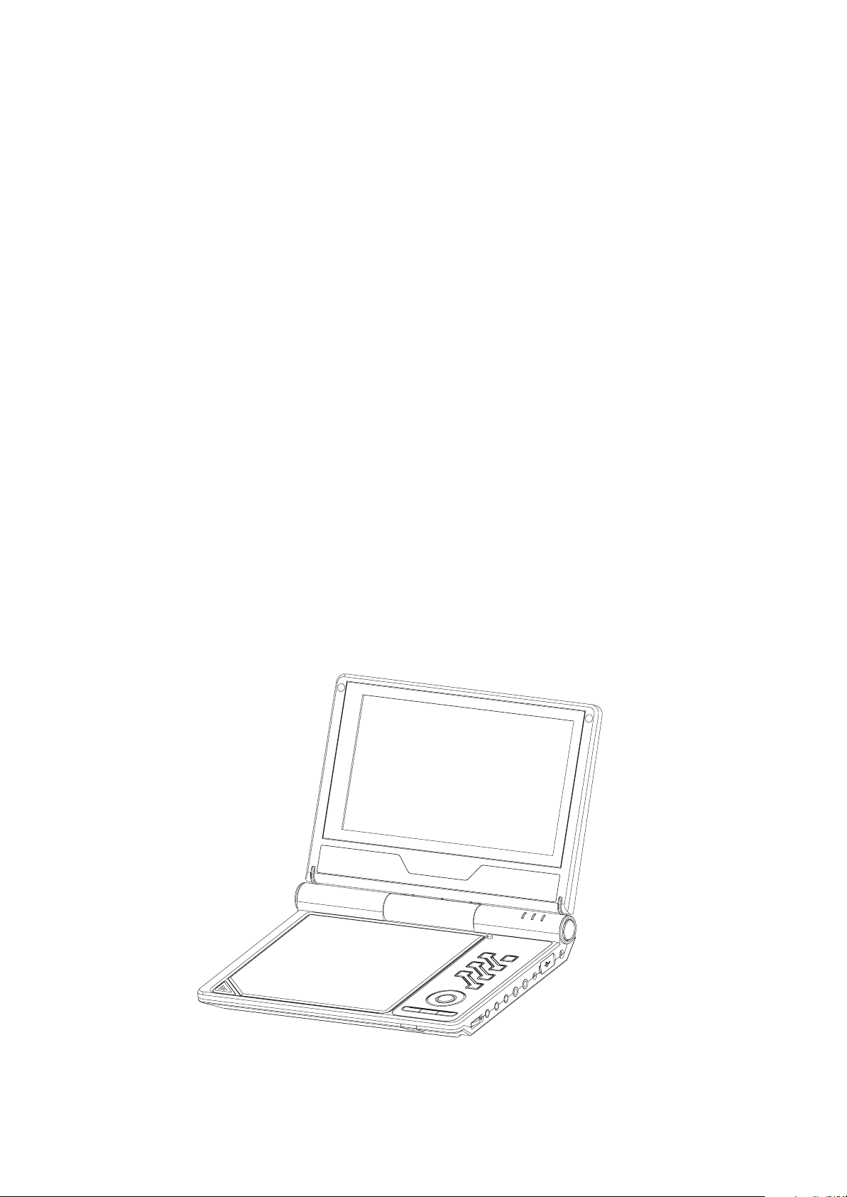
Control Button Locations and Explanations
2
1
2
22
21
3
4
5
6
7
8
9
10
11
1
Color TFT LCD
2
Speakers
3
DVD/AV INPUT button
4
PICTURE button
5
SETUP button
6
PLAY button / SELECT
button
7
PREV button / LEFT direction arrow
8
OPEN/CLOSE button
9
REW button
10
IR sensor
11
FWD button
12
PAUSE button / DOWN
direction arrow
13
Keyboard/Switch Button
14
NEXT button / RIGHT
direction arrow
15
STOP button / UP direction
arrow
16
MENU Button
17
Browser Button
18
LOGO Button
19
DVD/READER Button
20
AV INPUT indicator light
21
READER indicator light
22
DVD indicator light
20
19
18
17
16
15
14
13
12
Page 5
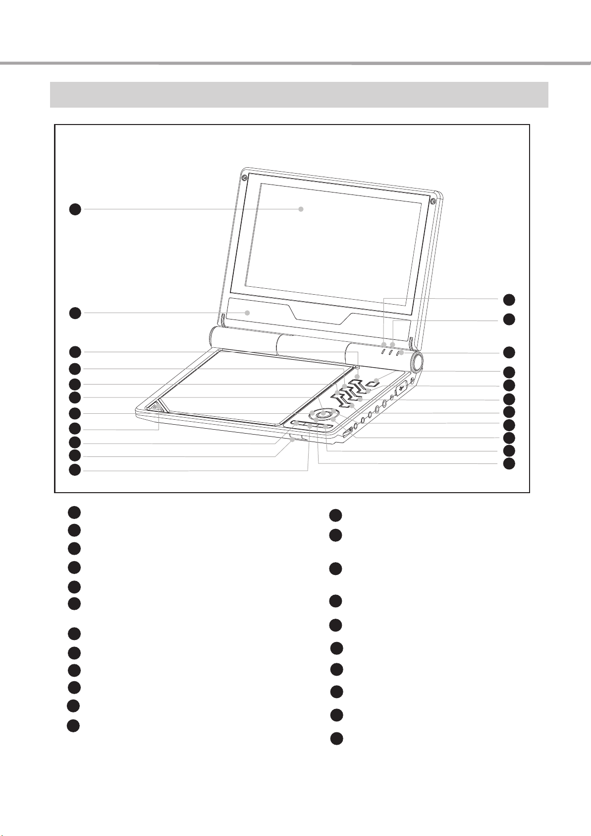
Remote Control Illustration
3
STANDBY Button
Press once to stand by, Press twice to play.
2
35
10
11
12
13
14
15
16
17
18
2
3
4
5
6
7
8
9
27
MENU Button
34
33
32
31
30
29
28
27
26
25
24
23
22
21
20
19
Display DVD menu or open/close PBC.
28
A-B Button
Repeat the select.
29
REPEAT Button
Repeat play.
30
RETURN Button
Back to the previous menu/Clearing
input numbers.
31
27
Q-PLAY Button
Skip the advertisement/warning and play
DVD directly.
32
27
PIC Button
Set video.
33
27
NUMBER Buttons
34
SUBTITLE Button
Change subtitle languages/
Switch JPEG display modes.
35
OSD Button
Display or hide disc information.
AUDIO Button
Change the audio language or
audio channel.
3
GOTO button
Play from the desired location.
4
ZOOM Button
Zoom in /out the displayed frame.
5
ANGLE Button
Change camera angles, MP3/JPEG
playback modes switch.
6
MUTE button
Press once to mute, twice to unmute.
7
TITLE button
DVD titles.
8
CURSOR Buttons
9
SELECT Button
10
SETUP Button
Function setup.
11
PLAY Button
Normal playback.
12
STOP Button
Stop playback.
13
REW Button
Fast backward play.
14
FWD Button
Fast forward play.
15
KEY Button
Fall tone.
16
KEY Button
Rise tone.
17
P/N Button
Switch the TV system between
PAL, NTSC and AUTO.
18
LOGO Button
Set the played image as the power-on logo.
19
SF Button
Adjusting sound field effects.
EQ Button
20
Adjusting equalization effects.
21
VOLUME-
Decrease volume.
22
VOLUME+
Increase volume.
23
PREV Button
Skip backward.
24
NEXT Button
Skip forward.
25
PAUSE Button
Pause frame by frame.
26
SLOW Button
Slow play.
Page 6
The laser diode in the traverse unit (optical pickup)may brake down due to static electricity of clothes or human
body. Use due caution to electrostatic breakdown when servicing and handling the laser diode.
Some devices such as the DVD player use the optical pickup(laser diode)and the optical pickup will be damaged
by static electricity in the working environment.Proceed servicing works under the working environment where
1. Put a conductive material(sheet)or iron sheet on the area where the optical pickup is placed,and ground the
3. The flexible cable may be cut off if an excessive force is applied to it.Use caution when handling the cable.
4
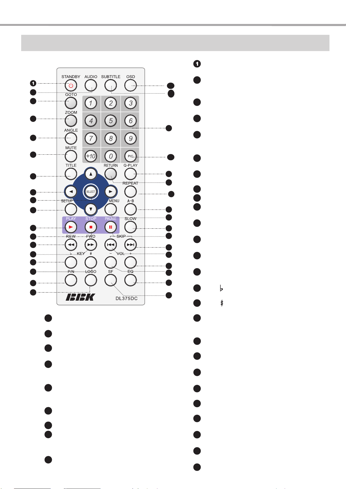
4.PREVENTION OF STATIC ELECTRICITY DISCHARGE
4.1.Grounding for electrostatic breakdown prevention
grounding works is completed.
4.1.1. Worktable grounding
sheet.
4.1.2.Human body grounding
1 Use the anti-static wrist strap to discharge the static electricity from your body.
safety_3 (1577x409x2 tiff)
4.1.3.Handling of optical pickup
1. To keep the good quality of the optical pickup maintenance parts during transportation and before
installation, the both ends of the laser diode are short-circuited.After replacing the parts with new ones,
remove the short circuit according to the correct procedure. (See this Technical Guide).
2. Do not use a tester to check the laser diode for the optical pickup .Failure to do so willdamage the laser
diode due to the power supply in the tester.
4.2. Handling precautions for Traverse Unit (Optical Pickup)
1. Do not give a considerable shock to the traverse unit(optical pickup)as it has an extremely high-precise
structure.
2. When replacing the optical pickup, install the flexible cable and cut is short land with a nipper. See the
optical pickup replacement procedure in this Technical Guide. Before replacing the traverse unit, remove
the short pin for preventingstatic electricity and install a new unit.Connect the connector as short times as
possible.
4. The half-fixed resistor for laser power adjustment cannot be adjusted. Do not turn the resistor.
Page 7
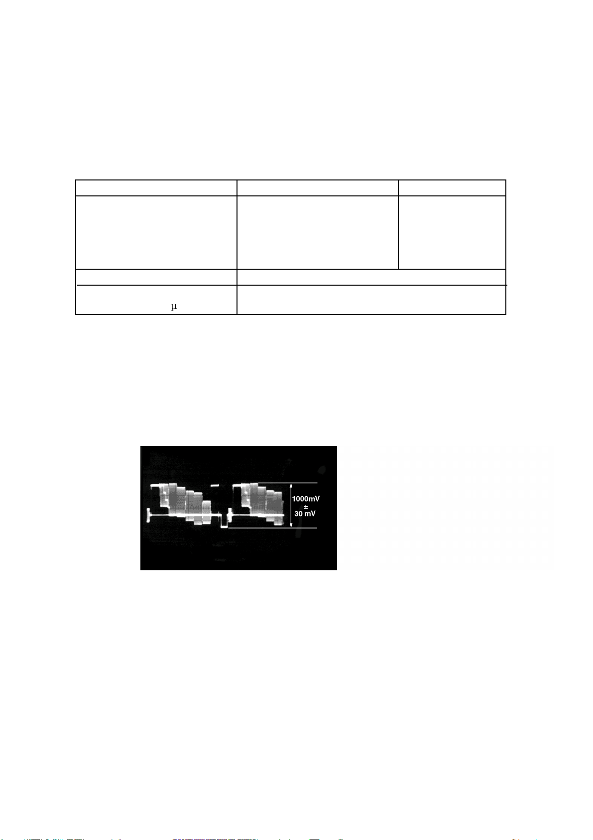
5.1. Video Output (Luminance Signal) Confirmation
5
5.Electrical Confirmation
DO this confirmation after replacing a P.C.B.
Measurement point
Video output terminal
Measuring equipment,tools
200mV/dir,10 sec/dir
Purpose:To maintain video signal output compatibility.
1.Connect the oscilloscope to the video output terminal and terminate at 75 ohms.
2.Confirm that luminance signal(Y+S)level is 1000mVp-p±30mV
PLAY(Title 46):DVDT-S15
PLAY(Title 12):DVDT-S01
Mode Disc
Color bar 75%
Confirmation value
1000mVp-p±30mV
DVDT-S15
or
DVDT-S01
Page 8
Do the confirmation after replacing P.C.B.
Screwdriver,Oscilloscope
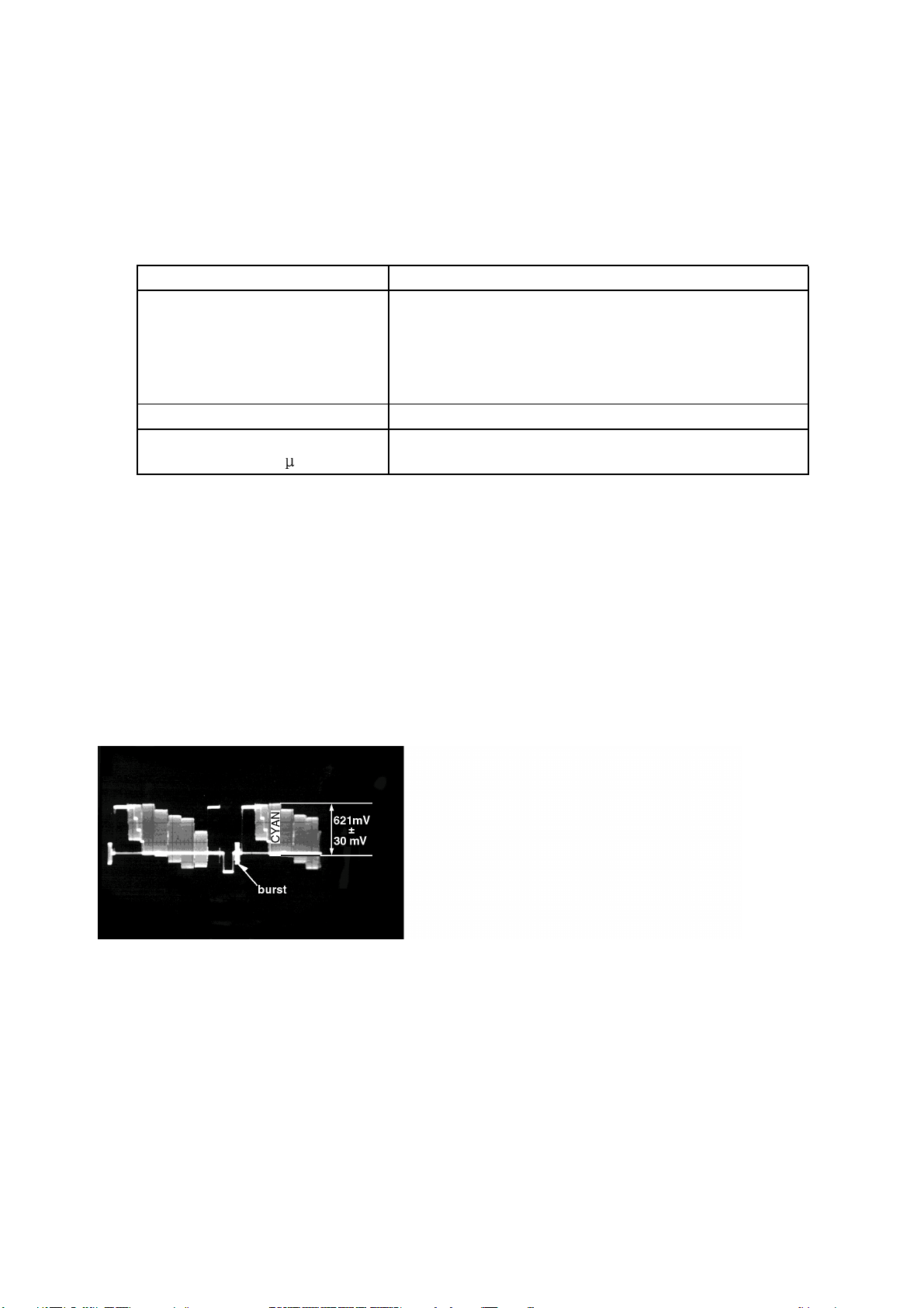
5.2 Video Output(Chrominance Signal) Confirmation
6
Measurement point
Video output terminal
Measuring equipment,tools Confirmation value
200mV/dir,10 sec/dir
Purpose:To maintain video signal output compatibility.
1.Connect the oscilloscope to the video output terminal and terminate at 75 ohme.
2.Confirm that the chrominance signal(C)level is 621 mVp-p±30mV
PLAY(Title 46):DVDT-S15
PLAY(Title 12):DVDT-S01
Mode Disc
Color bar 75%
621mVp-p±30mV
DVDT-S15
or
DVDT-S01
Page 9
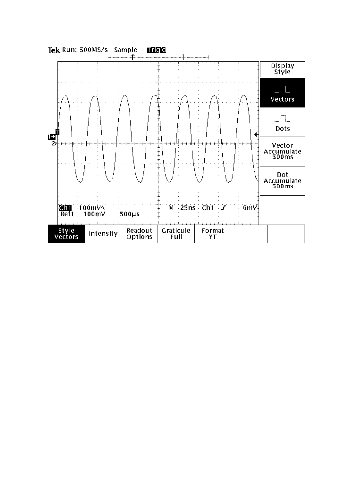
6.MPEG BOARD CHECK WAVEFORM
6.1 27MHz WAVEFORM
7
Page 10
7.2 MT1389
8
MT1389
Specifications are subject to change without notice
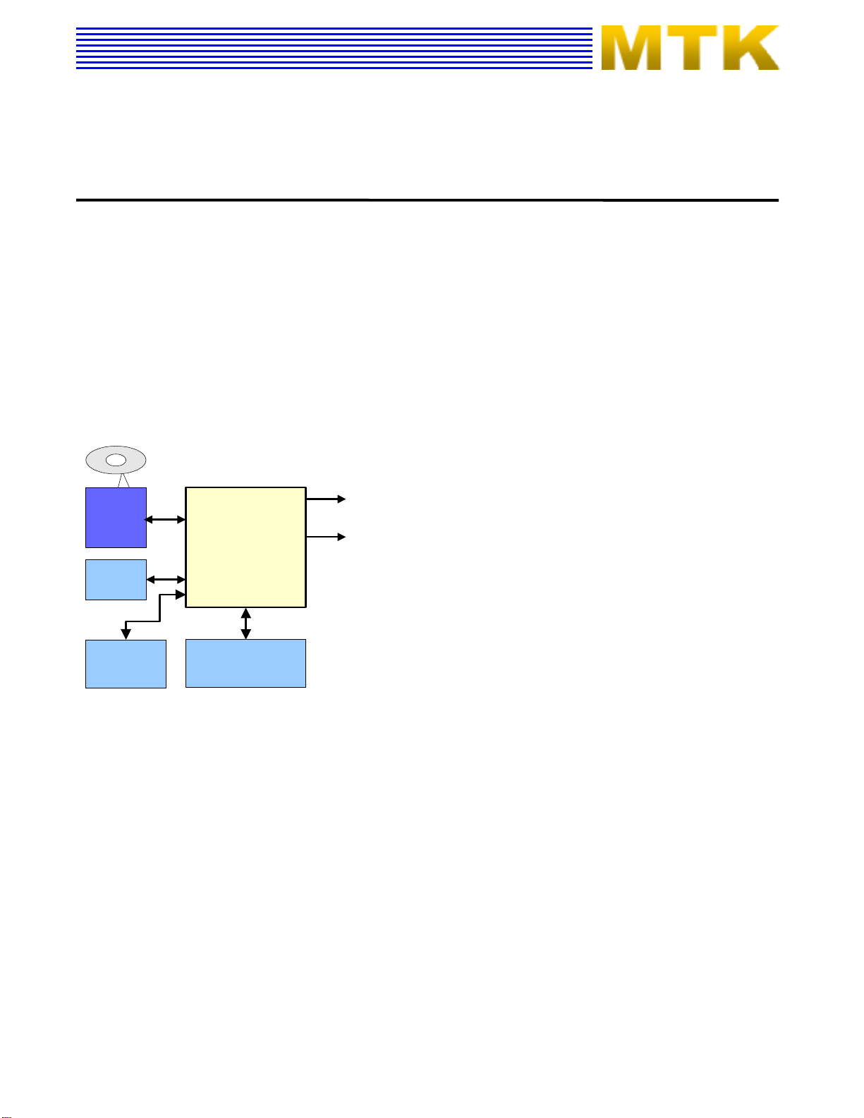
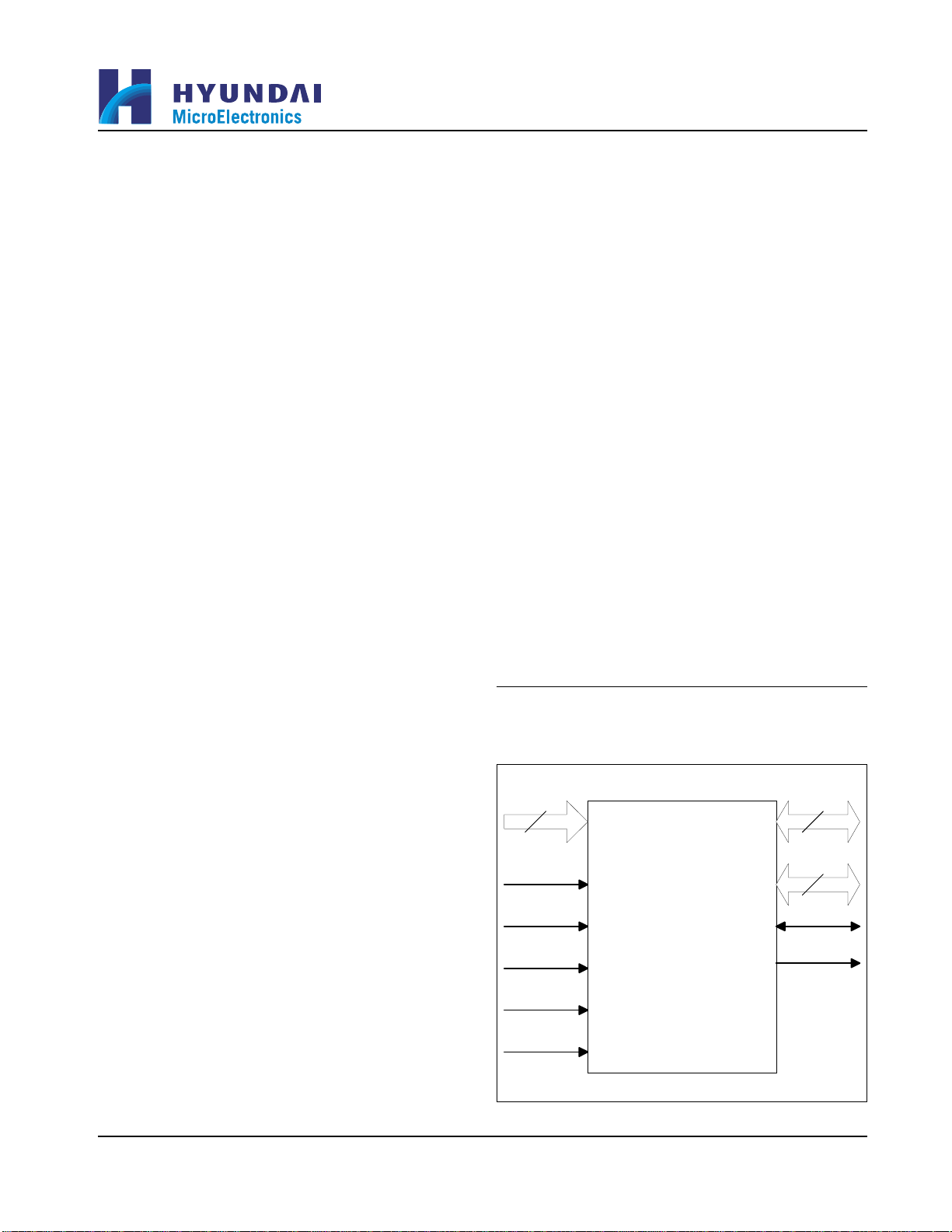
Progressive-Scan DVD Player SOC
MediaTek MT1389 is a DVD player system-on-chip (SOC) which incorporates advanced features like high
quality TV encoder and state-of-art de-interlace processing. The MT1389 enables consumer electronics
manufacturers to build high quality, cost-effective DVD players, portable DVD players or any other home
entertainment audio/video devices.
rd
Based on MediaTek’s world-leading DVD player SOC architecture, the MT1389 is the 3
player SOC. It integrates the MediaTek 2
decoder.
The progressive scan of the MT1389 utilized a proprietary advanced motion-adaptive de-interlace algorithm to
achieve the best movie/video playback. It can easily detect 3:2/2:2 pull down source and restore the correct
original pictures. It also supports a patent-pending edge-preserving algorithm to remove the saw-tooth effect.
nd
generation front-end analog RF amplifier and the Servo/MPEG AV
generation of the DVD
Key Features
RF/Servo/MPEG Integration
High Performance Audio Processor
Motion-Adaptive, Edge-Preserving De-interlace
108MHz/12-bit, 6 CH TV Encoder
Applications
Standard DVD Players
Portable DVD Players
DVD
PUH
Module
FLASH
Front-panel
Remote
CVBS, Y/C,
Component
SDPIF
MT1389HD
Audio DAC
DRAM
DVD Player System Diagram Using MT1389
Page 11

9
PRELIMINARY, SUBJECT TO CHANGE WITHOUT NOTICE MTK CONFIDENTIAL, NO DISCLOSURE
MT1389
General Feature List
1024-bytes on-chip RAM
Super Integration DVD player single chip
High performance analog RF amplifier
Servo controller and data channel processing
MPEG-1/MPEG-2/JPEG video
Dolby AC-3/DTS/DVD-Audio
Unified memory architecture
Versatile video scaling & quality
enhancement
OSD & Sub-picture
2-D graphic engine
Built-in clock generator
Built-in high quality TV encoder
Built-in progressive video processor
Audio effect post-processor
Audio input port
Up to 4M bytes FLASH-programming
interface
Supports 5/3.3-Volt. FLASH interface
Supports power-down mode
Supports additional serial port
DVD-ROM/CD-ROM Decoding Logic
High-speed ECC logic capable of correcting
one error per each P-codeword or
Q-codeword
Automatic sector Mode and Form detection
Automatic sector Header verification
Decoder Error Notification Interrupt that
signals various decoder errors
Provide error correction acceleration
High Performance Analog RF Amplifier
Programmable fc
Dual automatic laser power control
Defect and blank detection
RF level signal generator
Speed Performance on Servo/Channel Decoding
DVD-ROM up to 4XS
CD-ROM up to 24XS
Channel Data Processor
Digital data slicer for small jitter capability
Built-in high performance data PLL for
channel data demodulation
EFM/EFM+ data demodulation
Enhanced channel data frame sync protection
& DVD-ROM sector sync protection
Servo Control and Spindle Motor Control
Programmable frequency error gain and
phase error gain of spindle PLL to control
spindle motor on CLV and CAV mode
Built-in ADCs and DACs for digital servo
control
Provide 2 general PWM
Tray control can be PWM output or digital
output
Embedded Micro controller
Built-in 8032 micro controller
Built-in internal 373 and 8-bit programmable
lower address port
Buffer Memory Controller
Supports 16Mb/32Mb/64Mb/128Mb SDRAM
Supports 16-bit SDRAM data bus
Provide the self-refresh mode SDRAM
Block-based sector addressing
Support 3.3 Volt. DRAM Interface
Video Decode
Decodes MPEG1 video and MPEG2 main level,
main profile video (720/480 and 720x576)
Smooth digest view function with I, P and B
picture decoding
Baseline, extended-sequential and
progressive JPEG image decoding
Support CD-G titles
Video/OSD/SPU/HLI Processor
Arbitrary ratio vertical/horizontal scaling of
video, from 0.25X to 256X
65535/256/16/4/2-color bitmap format OSD,
256/16 color RLC format OSD
Automatic scrolling of OSD image
Slide show transition as DVD-Audio
Specification
2-D Graphic Engine
Support decode Text and Bitmap
Support line, rectangle and gradient fill
Support bitblt
Chroma key copy operation
Clip mask
Page 12

10
PRELIMINARY, SUBJECT TO CHANGE WITHOUT NOTICE MTK CONFIDENTIAL, NO DISCLOSURE
MT1389
Audio Effect Processing
Dolby Digital (AC-3)/EX decoding
DTS/DTS-ES decoding
MLP decoding for DVD-Audio
MPEG-1 layer 1/layer 2 audio decoding
MPEG-2 layer1/layer2 2-channel audio
High Definition Compatible Digital (HDCD)
Windows Media Audio (WMA)
Advanced Audio Coding (AAC)
Dolby ProLogic II
Concurrent multi-channel and downmix out
IEC 60958/61937 output
- PCM / bit stream / mute mode
- Custom IEC latency up to 2 frames
Pink noise and white noise generator
Karaoke functions
- Microphone echo
- Microphone tone control
- Vocal mute/vocal assistant
- Key shift up to +/- 8 keys
- Chorus/Flanger/Harmony/Reverb
Channel equalizer
3D surround processing include virtual
surround and speaker separation
TV Encoder
Six 108MHz/12bit DACs
Support NTSC, PAL-BDGHINM, PAL-60
Support 525p, 625p progressive TV format
Automatically turn off unconnected channels
Support PC monitor (VGA)
Support Macrovision 7.1 L1, Macrovision
525P and 625P
CGMS-A/WSS
Closed Caption
Progressive Output
Automatic detect film or video source
3:2 pull down source detection
Advanced Motion adaptive de-interlace
Edge Preserving
Minimum external memory requirement
Audio Input
Line-in/SPDIF-in for versatile audio
processing
Outline
256-pin LQFP package
3.3/1.8-Volt. Dual operating voltages
Page 13
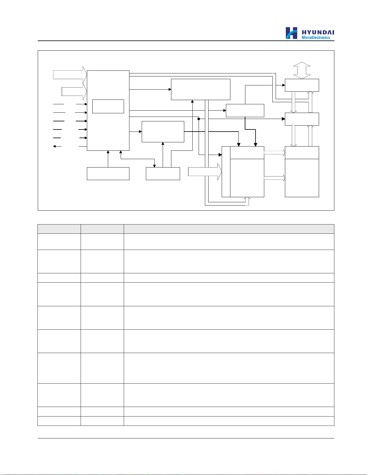
KEY FEATURES
IC BLOCK DIAGRAM & DESCRIPTION
11
HY29LV160
16 Mbit (2M x 8/1M x 16) Low Voltage Flash Memory
nn
n Single Power Supply Operation
nn
– Read, program and erase operations from
2.7 to 3.6 volts
– Ideal for battery-powered applications
nn
n High Performance
nn
– 70, 80, 90 and 120 ns access time
versions
nn
n Ultra-low Power Consumption (Typical
nn
Values At 5 Mhz)
– Automatic sleep mode current: 1 µA
– Standby mode current: 1 µA
– Read current: 9 mA
– Program/erase current: 20 mA
nn
n Flexible Sector Architecture:
nn
– One 16 KB, two 8 KB, one 32 KB and
thirty-one 64 KB sectors in byte mode
– One 8 KW, two 4 KW, one 16 KW and
thirty-one 32 KW sectors in word mode
– Top or bottom boot block configurations
available
nn
n Sector Protection
nn
– Allows locking of a sector or sectors to
prevent program or erase operations
within that sector
– Sectors lockable in-system or via
programming equipment
– Temporary Sector Unprotect allows
changes in locked sectors (requires high
voltage on RESET# pin)
nn
n Fast Program and Erase Times
nn
– Sector erase time: 0.25 sec typical for
each sector
– Chip erase time: 8 sec typical
– Byte program time: 9 µs typical
nn
n Unlock Bypass Program Command
nn
– Reduces programming time when issuing
multiple program command sequences
nn
n Automatic Erase Algorithm Preprograms
nn
and Erases Any Combination of Sectors
or the Entire Chip
nn
n Erase Suspend/Erase Resume
nn
– Suspends an erase operation to allow
reading data from, or programming data
to, a sector that is not being erased
– Erase Resume can then be invoked to
complete suspended erasure
nn
n Automatic Program Algorithm Writes and
nn
Verifies Data at Specified Addresses
nn
n 100,000 Write Cycles per Sector Minimum
nn
nn
n Data# Polling and Toggle Bits
nn
– Provide software confirmation of
completion of program and erase
operations
nn
n Ready/Busy# Pin
nn
– Provides hardware confirmation of
completion of program and erase
operations
nn
n Hardware Reset Pin (RESET#) Resets the
nn
Device to Reading Array Data
nn
n Compliant With Common Flash Memory
nn
Interface (CFI) Specification
– Flash device parameters stored directly
on the device
– Allows software driver to identify and use
a variety of different current and future
Flash products
nn
n Compatible With JEDEC standards
nn
– Pinout and software compatible with
single-power supply Flash devices
– Superior inadvertent write protection
nn
n Space Efficient Packaging
nn
– 48-pin TSOP and 48-ball FBGA packages
LOGIC DIAGRAM
20
A[19:0]
CE#
OE#
WE#
RESET#
BYTE#
DQ[7:0]
DQ[14:8]
DQ15/A-1
RY/BY#
8
7
Preliminary
Revision 1.0, June 2000
Page 14
HY29LV160
IC BLOCK DIAGRAM & DESCRIPTION
12
BLOCK DIAGRAM
DQ[15:0]
A[19:0], A-1
DQ[15:0]
WE#
CE#
OE#
BYTE#
RESET#
RY/BY#
STATE
CONTROL
COMMAND
REGISTER
VCC DETECTOR TIMER
SIGNAL DESCRIPTIONS
emaN epyT noitpircseD
]0:91[AstupnI
,]1-[A/]51[QD
]0:41[QD
#ETYBtupnI
#ECtupnI
#EOtupnI
#EWtupnI
#TESERtupnI
#YB/YR
V
CC
V
SS
--
--
ERASE VOLTAGE
GENERATOR AND
SECTOR SWITCHES
I/O CONTROL
PROGRAM
VOLTAGE
GENERATOR
Y-DECODER
A[19:0], A-1
X-DECODER
ADDRESS LATCH
I/O BUFFERS
DATA LATCH
Y-GATING
16 Mb FLASH
MEMORY
ARRAY
.hgiHevitca,sserddA nitupni]1-[A/]51[QDehthtiwdenibmoc,stupni02esehT
.snoitarepoetirwrodaerrofyarraehtnihtiwnoitacolenotceles,edometyB
stuptuO/stupnI
etats-irT
hgiHevitca,suBataD daerrofhtapatadtib-61ro-8naedivorpsnipesehT.
tib-12ehtfoBSLehtsadesusi]1-[A/]51[QD,edometyBnI.snoitarepoetirwdna
.edometyBnidetats-irtniamerdnadesunuera]8:41[QD.tupnisserddaetyb
.woLevitca,edoMetyB .edomdroWstceleshgiH,edometyBstceleswoL
.woLevitca,elbanEpihC romorfataddaerotdetressaebtsumtupnisihT
ehtdnadetats-irtsisubatadeht,hgiHnehW.061VL92YHehtotatadetirw
.edomybdnatSehtnidecalpsiecived
woLevitca,elbanEtuptuO rofdetagendnasnoitarepodaerrofdetressA.
gniruddaersidrowaroetybarehtehwsenimreted#ETYB.snoitarepoetirw
.noitarepodaereht
.woLevitca,elbanEetirW secneuqesdnammocrosdnammocfognitirwslortnoC
noitarepoetirwA.yarrayromemehtfosrotcesesareroatadmargorpotredroni
hgiHsi#EOdnawoLsi#ECelihwdetressasi#EWnehwecalpsekat.
.woLevitca,teseRerawdraH ehtgnitteserfodohtemerawdrahasedivorP
yletaidemmiti,tesersiecivedehtnehW.etatsyarradaerehtot061VL92YH
ecivedeht,detressasi#TESERelihW.ssergorpninoitarepoynasetanimret
.edomybdnatSehtnieblliw
tuptuO
niarDnepO
.sutatSysuB/ydaeR nisidnammocesareroetirwarehtehwsetacidnI
ylevitcasiecivedehtelihwwoLsniameR.detelpmocneebsahrossergorp
.atadyarradaerotydaersitinehwhgiHseogdna,gnisareroatadgnimmargorp
.ylppusrewop)lanimon(tlov-3
.dnuorglangisdnarewoP
Rev. 1.0/Jun 00
3
Page 15

PIN CONFIGURATIONS
IC BLOCK DIAGRAM & DESCRIPTION
13
HY29LV160
48-Ball FBGA (Bottom View)
A6 B6 C6 D6 E6 F6 G6
A[13] A[12] A[14] A[15] A[16] BYTE# DQ[15]/A[-1] V
A5 B5 C5 D5 E5 F5 G5 H5
A[9] A[8] A[10] A[11] DQ[7] DQ[14] DQ[13] DQ[6]
A4 B4 C4
WE# RESET# NC A[19] DQ[5] DQ[12] V
A3 B3 C3
RY/BY# NC A[18] NC DQ[2] DQ[10] DQ[11] DQ[3]
A2 B2 C2 D2 E2 F2 G2 H2
A[7] A[17] A[6] A[5] DQ[0] DQ[8] DQ[9] DQ[1]
A1 B1 C1 D1 E1 F1 G1
A[3] A[4] A[2] A[1] A[0] CE# OE# V
A[15]
A[14]
A[13]
A[12]
A[11]
A[10]
A[9]
A[8]
A[19]
NC
10
WE#
RESET#1112
NC
NC
RY/BY#
A[18]
A[17]
A[7]
A[6]
A[5]
A[4]
A[3]
A[2]
A[1]
13
14
15
16
17
18
19
20
21
22
23
24
H6
SS
D4
D3
1
2
3
4
5
6
7
8
9
Standard
TSOP48
E4 F4 G4 H4
DQ[4]
CC
E3 F3 G3 H3
H1
SS
48
47
46
45
44
43
42
41
40
39
38
37
36
35
34
33
32
31
30
29
28
27
26
25
A[16]
BYTE#
V
SS
DQ[15]/A[-1]
DQ[7]
DQ[14]
DQ[6]
DQ[13]
DQ[5]
DQ[12]
DQ[4]
V
CC
DQ[11]
DQ[3]
DQ[10]
DQ[2]
DQ[9]
DQ[1]
DQ[8]
DQ[0]
OE#
V
SS
CE#
A[0]
4
Rev. 1.0/Jun 00
Page 16

HY57V641620HG
14
7.4 HY57V641620HG
4 Banks x 1M x 16Bit Synchronous DRAM
DESCRIPTION
The Hyundai HY57V641620HG is a 67,108,864-bit CMOS Synchronous DRAM, ideally suited for the main memory applications which
require large memory density and high bandwidth. HY57V641620HG is organized as 4banks of 1,048,576x16.
HY57V641620HG is offering fully synchronous operation referenced to a positive edge of the clock. All inputs and outputs are synchronized with the rising edge of the clock input. The data paths are internally pipelined to achieve very high bandwidth. All input and output
voltage levels are compatible with LVTTL.
Programmable options include the length of pipeline (Read latency of 2 or 3), the number of consecutive read or write cycles initiated
by a single control command (Burst length of 1,2,4,8 or Full page), and the burst count sequence(sequential or interleave). A burst of
read or write cycles in progress can be terminated by a burst terminate command or can be interrupted and replaced by a new burst
read or write command on any cycle. (This pipelined design is not restricted by a `2N` rule.)
FEATURES
• Single 3.3±0.3V power supply
• All device pins are compatible with LVTTL interface
• JEDEC standard 400mil 54pin TSOP-II with 0.8mm
of pin pitch
• All inputs and outputs referenced to positive edge of
system clock
• Data mask function by UDQM or LDQM
• Internal four banks operation
Note)
• Auto refresh and self refresh
• 4096 refresh cycles / 64ms
• Programmable Burst Length and Burst Type
- 1, 2, 4, 8 or Full page for Sequential Burst
- 1, 2, 4 or 8 for Interleave Burst
• Programmable CAS Latency ; 2, 3 Clocks
.
Page 17

PIN CONFIGURATION
15
HY57V641620HG
VDD
DQ0
VDDQ
DQ1
DQ2
VSSQ
DQ3
DQ4
VDDQ
DQ5
DQ6
VSSQ
DQ7
DD
V
LDQM
/WE
/CAS
/RAS
/CS
BA0
BA1
A10/AP
A0
A1
A2
A3
DD
V
1
2
3
4
5
6
7
8
9
10
11
12
13
14
15
16
17
18
19
20
21
22
23
24
25
26
27
54pin TSOP II
400mil x 875mil
0.8mm pin pitch
VSS
54
DQ15
53
VSSQ
52
DQ14
51
DQ13
50
VDDQ
49
DQ12
48
DQ11
47
VSSQ
46
DQ10
45
DQ9
44
VDDQ
43
DQ8
42
SS
V
41
NC
40
UDQM
39
CLK
38
CKE
37
NC
36
A11
35
A9
34
A8
33
A7
32
A6
31
A5
30
A4
29
SS
V
28
PIN DESCRIPTION
PIN PIN NAME DESCRIPTION
CLK Clock
CKE Clock Enable
CS Chip Select Enables or disables all inputs except CLK, CKE and DQM
BA0,BA1 Bank Address
A0 ~ A11 Address
Row Address Strobe,
RAS, CAS, WE
LDQM, UDQM Data Input/Output Mask Controls output buffers in read mode and masks input data in write mode
DQ0 ~ DQ15 Data Input/Output Multiplexed data input / output pin
VDD/VSS Power Supply/Ground Power supply for internal circuits and input buffers
VDDQ/VSSQ Data Output Power/Ground Power supply for output buffers
NC No Connection No connection
Column Address Strobe,
Write Enable
The system clock input. All other inputs are registered to the SDRAM on the
rising edge of CLK
Controls internal clock signal and when deactivated, the SDRAM will be one
of the states among power down, suspend or self refresh
Selects bank to be activated during RAS activity
Selects bank to be read/written during CAS activity
Row Address : RA0 ~ RA11, Column Address : CA0 ~ CA7
Auto-precharge flag : A10
RAS, CAS and WE define the operation
Refer function truth table for details
Page 18

FUNCTIONAL BLOCK DIAGRAM
I/O Buffer & Logic
16
1Mbit x 4banks x 16 I/O Synchronous DRAM
HY57V641620HG
Self refresh logic
& timer
CLK
CKE
CS
RAS
CAS
WE
UDQM
LDQM
Row active
State Machine
refresh
Column
Active
Internal Row
counter
Row
Pre
Decoders
Column
Pre
Decoders
1Mx16 Bank 3
X decoders
1Mx16 Bank 2
X decoders
X decoders
1Mx16 Bank 1
1Mx16 Bank 0
X decoders
Memory
Y decoders
Cell
Array
Sense AMP & I/O Gate
DQ0
DQ1
DQ14
DQ15
Bank Select
A0
A1
A11
BA0
BA1
Address buffers
Address
Registers
Mode Registers
Column Add
Counter
Burst
Counter
CAS Latency
Data Out Control
Pipe Line Control
Page 19

A
8.SCHEMATIC & P.C.B WIRING DIAGRAM
DECODE BOARD
17
B
C
D
F
1.0
XS2
2341568
9107
111213
6
DV33
5
23 4
1
RN7
5
6
7
8
RN8
5
6
7
8
AVCC
R145
CE
R98
FBSMT
FBSMT
FBSMT
FBSMT
FBSMT
FBSMT
FBSMT
FBSMT
L67
L68
L69
L70
L71
L72
L73
876
123
KEY1
10K
L74
LED_USB
LED_CARD
LED_DVD
KEY_4
KEY_5
876
5
5
RN5 150R
123
4
4
KEY2
KEY3
KEY4
KEY5
KEY6
KEY7
KEY8
SDA
SCL
C82
104
8
R143
FBSMT
PUH5V
7
6
VCC
RST/WP
DC/NC1RST_/NC2WP/RST_3VSS
100K
B
TC1
C3
SUBD
SUBAAIOA
102(DNS)
C81
102(DNS)
5
SCL
SDA
EEPROM
4
V23
2SK3018-S
C E
V22
2SK3018-S
47uF/10V
104
D
RFO
R26
680R
R25
680R
C1
U1
AT24C16X4050
V20
3904-S
VCC
L1
30
XS1
10K
4
3
2
1
10K
4
3
2
1
RN6150R
DV33
IOA
10K
R166
B
100K
A
XS14
14
VCC
LED_CTL
VCC
DV33
L7
FBSMT
TC15
47uF/10V
LDO-AV33
R47
4.7R
CBSUBB
SUBC
104
C2
TDI
V20
B
U2
1.5K
LDO1
VR-CD
V4
2SB1132-S
VR-DVD
MDI1
AZ431-2.5V SOT-23-3
VCC
LOW_POWER2
R58
4.7K
VCC
C91
104
678
LM393
U3
123
4 5
R57
4.7K
VCC
LOW_POWER 1
R52
15K±1%
R51
1K±1%
R50
20K±1%
C83
104
P_VDD
TC18
10uF/16V
L22
10uH 2012
+9VIN
R167
DV33
LDO-AV33
LDO2
TC16
47uF/10V
V5
2SB1132-S
R48
4.7R
10uH 2012
10uH 2012
L3
L5
T+
F+
F-
LD-CD
LD-DVD
PUH5V
T-
2341568910711121415161317182021221923242627282529
XS30
R49
C
U5
TRIN
10K
SW1
关仓检测开关
IR遥控 输入电路
GND2VCC3OUT
HS0038B
1
R70
10R
47uF/10V
TC3
C92 103
IR
SW4P/3.2
+5.5V
MO_VCC
R69 1.2K
CPU5V
MO_VCC
TC2
47uF/10V
27
26
104
U4
C8
R68
R67
R66
L6
FCM2012-120T2A
F+
F-
T+
T-
V1P4
TC19
C7
104
1R
1R
1R
R65
R64
30
29
R63
R62
22uF/16V
VCC25VM1
VM2
RNF
28
LIMITH-HW-
234156891071112141513
XS3
1R
SP-
SP+
1R
13
11
12
14
VO2+
VOFC-
VOFC+
GND
GND
VOTK+15VOTK-16VOLD+17VOLD-18PGND19VNFTK20PVCC2
1R
1R
SL+
SL-
MO_VCC
D
R1
VOSL-
FG
24
FG
A32A24A1
WVU
HW+
10
PGND
VD1
DV33
R10
20K
STBY
V1P4
DMSO
22
23
21
PS
EC
ECR
H1+9H1-10H2+11H2-12H3+13H3-14VH
7
HU+
C14
C13
C12
HV-
HV+
HU-
R9
10K
8
9
VCC
PVCC1
21
C10
C9
TC4
URST#
R77
1N4148
10K
R(DNS)
R76
18
17
16
FR20SB
BR
CNF
HU-
HV+
HV-
HW+
HW-
104
104
104
HU+H+UVW
151
C95
R72 20K
V1P4
3
6
5
7
4
VOSL
VINSL-
VINSL+
VINFFC
PREGND22VINLD23CTK224CTK125VINTK26BIAS27STBY
TRSO
R71 20K
FMSO
104
104
C94 151
47uF/10V
E
10K
C96
TVS(DNS)
TC20
10uF/16V
BBK
比例 质量 数量
6
第 1 张 共 5张 版次:
广东步步高电子工业有限公司AV厂
2379-2
DL379
104
C16
104
C15
8
29
HSOP28/SMD
G1
GND
G2
BA6849/6869
15
30
47R
R75
H-
R74
47R
MO_VCC
SL-
SL+
XS15
FOSO
1
CF12CF2
VINFC
U6
BA5954
28
V1P4
STBY
R8
10K
C11
104
DM-12接口电路
设 计
更改 数量 更改单号 签 名 日期
审 核
标准化
板号:
5
批 准
1234
F
Page 20

A
18
XI
XO
R1860RR187
R4 100K
6
DMA5
DMA4
R78
33R
R79
DMA5#
DMA4#
5
DV33
100UH
10UH
L24
L25
ADACVDD
APLLVDD3
C26 104
R5
1K
89V33
TC41
V18
100uF/6.3V
C25
104
TC22
10uF/16V
TC44
T10uF/16V
TC40
C117
475
100uF/6.3V
TC46
RFV18
TC59
0.47uF
C112
TC21 10uF/16V
20pF
C111
C107
1000pF
100K
V1P4
R3
104
C24
0.033uF
C106
104
C23
104
C22
23 4
15K
R86
PLLVDD3
TC5
47uF/10V
ADCVDD3
C17
104
4.7RL9FBSMT
L23
1
RFV33
DQ0
DQ1
DQ2
DQ4
DQ5
DQ6
DQ7
DQ3
0R
C119
27pF
DQ02DQ14DQ25DQ37DQ48DQ510DQ611DQ713DQ842DQ9
X1
33R
C18
A023A124A225A326A429A530A631A732A833A934A10/AP22A1135BA0/A1320BA1/A1221CLK38CKE37/CS19/RAS18/CAS17/WE16DQML15DQMH39NC36NC40VSS54VSS41VSS
27MHz
U7
27pF
C118
DMA0#
DMA1#
DMA2#
DMA3#
DMA4#
DMA5#
DMA6#
DMA7#
R85
DMA11
R84
BA0
BA1
R81
R91 750K
TC23
10uF/16V
V18
89V33
FS
VREF
ABCK
ACLK
SPDIF
AVCM
XTALI
JITFO
JITFN
LPFIP
LPFIN
LPFOP
OSP
OSN
RFGC
IREF
C97 1uF
BAD
C20
104
GPIO_4
GPIO_3
SPMCLK
SPDATA
SPLRCK
SPBCK
DVDD3
ALRCK
DVDD18
APLLCAP
APLLVSS
ARF(SW)
RFGND18
RFVDD18
XTALO
PLLVSS
PLLVDD3
LPFON
ADCVSS
RFVDD3
RFRPDC
RFRPAC
HRFZC
CRTPLP
RFGND
AVDD3
C98 1uF
YUV0/CIN
DACVDDC
ASDATA3
ASDATA4
MC_DATA
APLLVDD3
ADACVSS2
ADACVSS1
ALF/(CTR)
IDACEXLP
ADCVDD3
AGND
1
L14
192
DACVSSC
ARS/SDATA3
AR/SDATA1
AL/SDATA2
ALS/SDATA0
ADACVDD1
ADACVDD2
DVDA
2
C99 1uF
FBSMT
V18 RFV18
SY
191
190
YUV1/Y
ASDATA0/GPO_2
RVREF/GPIO_6
RCLKB/GPIO_5
ASDATA1/GPO_1
ASDATA2/GPO_0
DVDB3DVDC4DVDD
C100 1uF
C
104
104
104
193
194
195
196
197
198
199
200
201
202
203
204
205
206
207
208
209
210
211
212
213
214
215
216
217
218
219
220
221
222
223
224
225
226
227
228
229
230
231
232
233
234
235
236
237
238
239
240
241
242
243
244
245
246
247
248
249
250
251
252
253
254
255
256
C21
104
RFSVDD3
FBSMT
L11
L12
DACVDD3 DV33
C110
104
R80
DMA10# DMA10
FBSMT
510R
R90
FS
XO
XI
JITFO
JITFN
0.047uF
RFVDD3
FBSMT
L10
33R
FM_CTL
UP1_5
ASPDIF
APLLVDD3
89_AR
89_AL
UP1_4
UP1_3
ADACVDD
PLLVDD3
C109
ADCVDD3
RFVDD3
390pF
C29
C28
C27
ASDATA0
GPIO6
GPIO5
GPIO4
GPIO3
ASDATA1
ASDATA2
MS_CD
SD_CD
ASDATA3
0.047uF
AVDD3
C19
JITFNJITFO
C108
104
A
B
SD33
DQ8
DQ9
DQ10
DQ11
DQ12
DQ13
DQ14
44
DQ1045DQ1147DQ1248DQ1350DQ1451DQ15
DMA8#
DMA9#
DMA10#
MA11
#BA0
#BA1
33R
33R
1 2
33R
SDCLK
C188
DNS
STBTA
SC
CVBS
185
189
183
187
188
184
186
YUV2/C
YUV4/G
DACVSSB
DACVSSA
DACVDDB
DACVDDA
YUV3/CVBS
DVDRFIP6DVDRFIN7MA8MB9MC10MD11SA12SB13SC14SD15CDFON16CDFOP17TNI18TPI19MDI120MDI221LDO222LDO1
5
C101 1uF
DAB
C
RFO
104
C30
SD33
DQ15
27
53
VCC1VCC14VCC
DCS#
DRAS#
SDCLK
SDCKE
DCAS#
DWE#
876
5
33R
123
4
R83
R82 33RDCLK
RN1
CS#
RAS#
CAS#
WE#
DCKE
R43
10K
YUV7
VSYNC
HSYNC
IO_17
IO_0
182
176
181
179
180
178
177
DVSS
IO_17
YUV7
YUV5/B
YUV6/R
C0/IO_0
VSYNC/V_ADIN1
HSYNC/V_ADIN2
MT1389HD
SUBA
SUBB
SUBC
SUBD
TN1
C123
15P
C122
15P
C121
15P
C120
15P
RFV33
104
C31
TC42
L13
FBSMT
100uF/6.3V
DV33
B
VCCQ3VCCQ9VCCQ43VCCQ
DQM0
DQM1
33R
RN3
33R
R44
LOW_POWER 2
LOW_POWER 1
175
173
174
C1/IO_1
DVDD18
TP1
MDI1
C33
DMA0#
876
123
DMA0
C2/IO_2
C
TC24
49
52
VSSQ6VSSQ12VSSQ46VSSQ
28
DMA1#
DMA2#
DMA3#
DMA6#
DMA7#
DMA8#
5
876
4
123
DMA1
DMA2
DMA3
DMA6
DMA7
DMA8
10K
ASTB
BL_CTL
OUT+5V_CTL
MUTE_DAC
SHUTDOWN
172
171
169
167
168
166
170
DVDD3
C3/IO_3
C4/IO_4
C5/IO_5
C7/IO_7
C6/IO_6
YUVCLK/IO_8
Pin Assignment v1.5
V2REFO28SGND27VREFO30V2029TEO32FEO
RFLVL/RFO N26CSO/RFOP
SVDD3
23
25
24
RFOP
RFON
104
LDO2
LDO1
V2P8
RFSVDD3
10uF/16V
C40
104
C39
104
104
C38
SDRAM 64M
C37
104
C36
104
C35
104
SD33
C34
104
DMA9#
5
FBSMT
33R
L15
4
DV33
RN2
DMA9
KEY1
KEY2
KEY3
KEY4
KEY5
KEY6
KEY7
KEY8
165
160
164
163
162
161
159
158
157
Y0/IO_9
DVDD18
Y1/IO_10
Y2/IO_11
Y3/IO_12
Y4/IO_13
Y5/IO_14
Y6/IO_15
TEZISLV33OP_OUT34OP_INN35OP_INP36FOO42TRO41VPLLVDD3
31
37
DMO
FEO
TEO
TEZISLV
OPO
OP-
OP+
10K
V20
V1P4
C32 104
R11
DMSO
TC6
V2P8
C41
156
Y7/IO_16
FMO
15K
FMSO
47uF/10V
104
C
UPD[15..0]
DMA7
DMA6
DMA5
DMA4
155
154
153
152
RA4
RA5
RA6
DVDD3
TROPENPWM39PWMOUT1/V_ADIN940USB_VSS
FMO38DMO
TRO
FOO
TROPEN
18K
20K
R92
R73
R87
TRSO
FOSO
D
A17
GNDA0AD7
46
45
47
48
Vss
A16
BYTE
A151A142A133A115A106A88A199WE11RESET
U8 8/16/32M_FLASH(TSOP)
4
A15
A14
A13
A16
UPA[20..0]
VD
DMA9
DMA11
DCKE
DCLK
DMA8
149
147
151
150
146
148
RA7
RA8
RA9
CKE
RA11
DVSS
RCLK
VPLLVSS
CAPPAD44USBP47USBM48USB_VDD349FG/V_ADIN850TDI/V_ADIN4
43
45
46
USBP
USBM
VPLLVDD3
CAPPAD
C127
562
C126
330pF
FBSMT
C125
330pF
C93
103
L16
C124
89V33
V1P4
153
D
DQ15/A-1
A12
145
USBVDDFGTDI
44
A12
0R A20
DVDD3
AD14
DQ7
DQ1443DQ13
A11
DMA2
DMA3
144
143
RA3
51
104
AD6
AD13
AD5
AD12
AD4VDAD11
41
42
38
DQ6
DQ540DQ4
DQ1239DQ11
NC10NC
A9
7
A10
A9
AA21
DWR#
AA20
R99
R12 10K
R95 4.7K
R94 4.7K
R93 4.7K
R59 4.7K
BA1
DMA10
DMA0
DMA1
139
142
141
140
138
RA2
RA1
RA0
RA10
DVDD18
TMS/V_ADIN5
TCK/V_ADI N653TDO/V_ADIN754DVDD1855IOA2
52
56
TRIN
STBY
CTR_TFTA2A3A4A5A6A7A8A18
V18
C42
V20
V1P4
37
Vcc
12
BA0
137
BA1
AD3
AD10
34
36
35
14
13
RAS#
CS#
136
135
BA0
RCS#
RAS#
IOA5
IOA357IOA4
59
58
TC8
47uF/10V
C45
104
TC7
47uF/10V
C43
104
AD2
AD9
AD1
AD8
32
31
DQ830DQ9
DQ233DQ3
DQ1
DQ10
A619A1717RY/BY15A1816NC
18
A19
A18A7A6A5A4A3A2
A8
R100
4.7K(DNS)
LIMIT
CAS#
WE#
DQM1
132
133
134
130
131
CAS#
RWE#
DQM1
DVDD3
HIGHA062IOA18
IOA660IOA7
63
64
61
A19
BBK
DL379
DQ9
DQ10
DQ11
DQ12
DQ13
DQ14
DQ15
DQ0
DQ1
DQ2
DQ3
DQ4
DQ5
DQ6
DQ7
IOA
DQM0
INT0#
IR
URST#
TXD
RXD
TFT_SWITCH
L78100K
SDA
SCL
L77100K
L76100K
L75100K
A0
A17
V18
AD7
ALE
CTR_AUDIO
AD6
AD5
AD4
AD3
AD2
AD1
AD0
PRD#
A1
PCE#
A20
A9
A10
A11
A12
A13
A14
A15
A16
PWR#
104
104
C54
104
L21
FBSMT
F
1.0
6
比例 质量 数量
第 2 张 共5张 版次:
广东步步高电子工业有限公司AV厂
2379-2
解码原理图
5
板号:
设 计
审 核
标准化
更改 数量 更改单号 签 名 日期
DV33
V18
批 准
4.7K(DNS)
R60
DV33
LED_CTL
LED_USB
LED_CARD
LED_DVD
C61
104
RXD
TXD
GND
XS4
XS04(DNS)
231
4
DWR#
DCE#
DRD#
0R
0R
R23
R270RR28
PWR#
PCE#
PRD#
C60
104
C58
104
C56
104
C55
104
C53
104
C52
104
1234
F
E
AD0
DRD#
GND
DCE#
A1
27
29
28
25
CE26A0
OE
Vss
L19
DQ0
A520A421A322A7
DQ8
129
RD8
IO_18
IOA19
L17
FBSMT
TC25
VD DV33
10K
RD9
RD10
RD11
RD12
RD13
RD14
RD15
RD0
RD1
RD2
DVDD3
RD3
RD4
RD5
RD6
RD7
IO_19
DQM0
INT0#
IR
PRST#
ICE
UP3_5
UP3_4
UP3_1
UP3_0
UP1_7
UP1_6
UP1_5
UP1_4
UP1_3
UP1_2
DVDD3
URD#
UWR#
DVDD18
IOA0
A17
DVSS
AD7
ALE
IOA21
AD6
AD5
AD4
AD3
AD2
DVSS
AD1
AD0
IOCE#
IOA1
IOCS#
IOA20
HIGHA1
HIGHA2
HIGHA3
HIGHA4
HIGHA5
HIGHA6
HIGHA7
A16
IOWR#
DVDD3
C51
104
C50
104
C49
104
C48
104
C47
104
C46
104
C44
104
10uF/16V
C62
104
DV33
U9
MT1389HD
128
127
126
125
124
123
122
121
120
119
118
117
116
115
114
113
112
111
110
109
108
107
106
105
104
103
102
101
100
99
98
97
96
95
94
93
92
91
90
89
88
87
86
85
84
83
82
81
80
79
78
77
76
75
74
73
72
71
70
69
68
67
66
65
C59
C57
DV33A
VPLLVDD3
DV33A
AVDD3
L18
FBSMT
L20
FBSMT
A223A1
24
R2
89V33
FBSMT
DV33
E
Page 21

A
20
C
D
E
F
1.0
6
5
L1MUTE2DA3CL4CE5R6F-VCC7GND8RF
FM_L
D3
UP1_5
4
FM_L
C146 105
20K
R114
LLOUT
3
2
1
U11
UP1_4
FM_R
C147 105
20K
R115
RROUT
R107 33K
LL
AGND
TC9
C64
5
VD9
R128
C183
C6
ROUT1
ROUT
JK3
3274681
AGND
C182
102
C181
102
Y_TFT1
C180
20P
FBSMT
FBSMT
FBSMT
47uF/10V
L39
L38
L41
FM_GND
104
ALIN
Y_TFT
ARIN
GND
2
ce4vin
104
C63
FM_CTL
V5V
MMBD4148SE
C142
47PF
C141
47PF
150R
683
22R
R7
333
SPGND
SP5V
SCL
SDA
SP5V
C151
105
R30 0R
LOUT LOUT1
MUTE-1
2
1
V9
8550
VGND
R131
2.7K
+9VIN
C190
RSOUT-
RSOUT+
C189
683
22R
R32
SPGND
TC33
C153
C66
U13
1
2
3
4
5
6
7
C65
C152
R38
DNS
R31
DNS
C135
C191
333
C192
154
15uH
15uH
L29
L30
47uF/10V
105
104
SPGND
26
28
27
MAX9702
OUTL-
OUTL+
PVDD
SYNCH_OUT
SCL
SDA
BIAS
SYNC
CPVDD
C1P8CPGND9C1N10CPVSS11VSS12HPL13HPR
104
105
SPGND
C150 105
C155 105
SPGND
C
同轴输出
C149
1.8uH
RROUT
ROUT
7
JK2
3274681
LLOUT
100P
100R
FM_GND
VGND
20pF
C143
C_TFT
V5V
VD8
MMBD4148SE
2
1
C139
47PF
VGND
C137
47PF
L35
1.8uH
R126
75R
SC
SPGND
L31 FBSMT
L32
10uH 2012
VCC V5V
A8V
330R
R123
39K
T10uF/16V
R122
47K
U10B
4580
4 8
5
C131
122
AGND
LL
TC29
C130
102
47K
R120
T10uF/16V
ALIN
AV OUT
CVBS_OUT
RROUT
FM_VCC
vout1vout
U12
RT9701
3
VCC
Y_TFT1
3
C140
47PF
VGND
L36
1.8uH
C138
47PF
R127
150R
SY
LSOUT+
LSOUT-
C148
683
22R
R34
C4
333
C5
154
L8
L4
15uH CDRH4D28CLD
15uH CDRH4D28CLD
TC32
220uF/16V
AGND
RR
T10uF/16V
TC30
T10uF/16V
R121 47K
R29 0R
ARIN
B
JK1
421
3
C84 104
天线
R130
R129
120R
C185
102
ASPDIF
FM模块
FM_MODULE
9
FM_R
FM_GND
RFOUT
UP1_3
C184
L27
FBSMT
FM_VCC
FM_VCC
R117
R116
A8V
C132 101
R105
R103
R101
TC26
T10uF/16V
RFOUT#
L28
100uH
V8
R118
100K
2SC4226
104
CVBS_OUT
FBSMT
L37
D3
R36
0R(DNS)
1K
FM_GND
1K
VGND
FM_GND
C134
102
LLOUT
R111
100K
L26 FBSMT
LOUT
V6
2SC1815-Y
R109
330R
R110
MUTE-1
TC27
T10uF/16V
1
U10A
4580
4 8
3
2
C129
122
4.7K
4.7K
C128
102
6.8K
89_AL
3
R37
0R(DNS)
FM_GND
L34
CVBS
BL_GND
C136
102
AGND
R112
100K
V7
2SC1815-Y
560R
R125
R124
560R
TC31
A8V
R108 33K
6
C133 101
R106
4.7K
AGND
R104
4.7K
RR
R102
6.8K
TC28
89_AR
A
BL_9V
AV IN
AGND
FB120 0805
L40
123456789
CN1
静音电路
VD2
1N4148
V14
8050
R41
4.7K
R159
10K
683
MUTE_DAC
22R
R33
333
SPGND
HP
JK4
421
3
HP-L
HP-R
C166
105
C158
104
SPGND
22
24
23
PVDD
PGND25PGND
OUTR-
OUTR+
/SHDN
HPS
INM
INL
INR
GND
VDD
14
SPGND
SD05C
C_TFT
Y_TFT
SCL
SDA
VGND
BL_GND
BL_CTL#
VGND
LSOUT-
LSOUT+
+7.5V
+15V
-10V
RSOUT-
RSOUT+
VCC
GND
6
FBSMT
FBSMT
FBSMT
FBSMT
FBSMT
FBSMT
L44
L49
L50
L52
L53
L57
1011121314
SD_DAT2
JK6
1
IO_17
HSYNC
C168 20P
C167 20P
10K
10K
R148
R147
L42 FBSMT
DV33
JK5
HP
421
3
SPGND
HP-V2
HP-V1
15K
SP5V
FBSMT
FBSMT
L79
L80
21
20
19
18
17
16
15
C67
104
105
C154 105
C156
C157
105
SP5V
SP5V
R39
10K
R40
10K
TV1
SD05C
3
2
TV2
VR1
541
ROUT1
D
SPGND
DV33
50K*2
LOUT1
FB120 0805
FBSMT
FBSMT
FBSMT
FBSMT
L45
L46
L47
L48
L54
123456789
ASDATA1
GPIO3
GPIO4
ASDATA0
10K
10K
R153
R154
1N4148
VD7
1N4148
1K
1K
VD6
R137
R136
V10
8050
V24
8050
SPGND
8050
10K
FBSMT
L55
18
SPGND
VCC
FBSMT
C145
20PF
L58
C144
20PF
C196
101
C195
101
C194
104
C193
104
CN2
CON14
SD_CD/DAT33MS_VSS2SD_CMD6MS_VCC4MS_SCLK5SD_VSS19MS_D37MS_INS8SD_VDD11MS_D210SD_CLK14MS_D012MS_D113SD_VSS217MS_BS15MS_VSS16SD_DAT019SD_DAT1
ASDATA3
ASDATA2
MS_CD
GPIO5
GPIO6
10K
10K
10K
10K
R149
R151
R152
R150
R138
R135 15K
10K
R13
10K
SP5V
R184
SPGND
R97 4.7K
V15
/扬声器 耳机放大
R185
R45
10K
SHUTDOWN
E
比例 质量 数量
第 3 张 共6张 版次:
广东步步高电子工业有限公司AV厂
BBK
C200
104
C199
104
C198
104
DL379
C197
104
2379-2
INPUT&OUTPUT
5
板号:
CON9
驱动板接口
SD WP21SD CD GND22SD WP GND
SD/MMC/MS
20
C170
VSYNC
YUV7
SD_CD
C169
10K
10K
10K
R155
R156
R157
R14 10K
SPGND
R141
10K
R140
10K
设 计
审 核
标准化
更改 数量 更改单号 签 名 日期
20P
20P
104
C159
VCC1USBM2USBP3USB_GND4GND
JK7
USBVCC
33R
33R
R162
R161
L56 FBSMT
VCC
USBM
USBP
BL_CTL#
V17
8050
V16
8050
R139
10K
BL_CTL
批 准
USB
5
C68
104
TC34
10UF/16V
R89
15K
R88
15K
1234
F
Page 22

22
DECODE BOARD
Page 23

23
Page 24

A
BATTERY CHARGER
24
B
C
D
E
F
1.0
6
5
VOUT+VIN
R624
10K
G2
D2 S2
D2
QB601B
IRF7316
TC604
C609
C608
TC603
0390219
C607
102
L601
33uH
2
T11 VOUT+T12
C606
QB602
IR7416
R608
1K1206
23 4
R604
G1
D1 S1
D1
QB601A
IRF7316
R602
1K
VIN T10
1
TC601
VIN
100uF/16V(AL)
224
104
100uF/16V(AL)
VD602
MBRS340
A1K
102
R609
10R
Q605
8050
Q603
8050
Q604
8550
VD601
1N4148
T9
MOS_SW
TC602
100uF/16V AL
10K
R603
Q601
8050
100uF/16V AL
R601
10K
CVDD
R605
10K
4.7K
R617
4.7K
Q602
8050
C602
104
R616
Ref
K
U603
TL431
3
1
A
2
R615
A
J1
FUSE1
F1
3A
R623
3.3K
470R1206
R621
R620
10K
CVDD
R619
10K
R618
10K
P2.6/AD811P0.7/AD712P0.6/AD613P0.5/AD514P0.4/AD415P0.3/AD316P0.2/AD217P0.1/AD118P0.0/AD0
TC606
T47uF/10V
U604
10
10K_1%
10K_1%
B
BBK
AV
1
6
1
B379-1
DL379
Battery Charge circuit
5
XIN
XOUT
R667
123
JK601
VIN
GND
TVS(DNS)
R668
TVS(DNS)
4
BA-CON
C622
10pF
R666 100K
X601
8MHz
10pF
C621
VIN
VOUT+
1
2
1
2
GND
3
3
DCB_IN1
DC1.5
R648
100R1206
R647
100R1206
Q606
8050
104
C615
R645
22K 1%
R643
*
R643/R644 1M~4.7M
R622
4.7K
R636
10K
MOS_SW
T3T4T5
R632
220K
CVDD
R631
470R1206
R646
22K 1%
R644
*
R642
0.27R
VOUT-
R641
0.27R
R640
0.27R
R639
0.27R
R638
0.27R
C627
104
678
U605
123
4 5
T7
R635
470R
TEMP
470R
R634
R625
4.7K
R633
XOUT
C614
C626
T47uF/10V
CVDD
LM358M
R658
1.5K_1%
R637 24K
C620 104
104
C619
47K
CVDD
T8
C618
T47uF/10V
20
19
C617
104
VDD
VSS1XIN/P1.02XOUT/P1.13/RE/P1.24P2.05P2.16P2.27P2.38P2.49P2.5
S3C9454
XIN
T6
104
1
1
2
R657
2.2K
2
QB603B
IRF7316
L602
FB120
CB1 104 CB2 104
QB603A
IRF7316
RB10
5.1K
RB9
1M
G2
D2 S2
D2
D1S1
D1
G1
T2
RB8
5.1K
2
DOP1COP
U602 S8253
RB7
0R
3
4
CTL
VMP
VSS5VC26VC17VDD
8
C8
104
CB8
2.2UF
RB11
BT2
BATTERY
B+
RED
B+
RB4
B
RB5 1K
CB7
104
1K
8
7
VCC
SENS1DO2CO3VM
RB3
1K
RB6
51R
1K
BT1
BATTERY
B
WHITE
CB6
104
CB5
104
6
5
VC
ICT
VSS
S8232G
UB1
S8232G
4
T1
4.7M
1K
LED601
R649
470R1206
RG
C
D
E
B-
BLACK
B-
QB1B
UPA1870
QB1A
UPA1870
RB2
RB1
RP1
NTC 10K
TEMP
CB3 104 CB4 104
1234
VOUT-
F
Page 25

BATTERY CHARGER
25
Page 26

D
MAIN FRONT PANEL
26
4
/
321
/
/
/ /
DVD/U/
SW7 SW11 SW15
C
VCC_M
R16
100R
VCC_M
R15
100R
VCC_M
R14
100R
B
LED
USB
D13
D12
D11
C14
LED
C13
LED
C12
104
104
DVD
104
V4
8050
R46
1K
LED_USB
V3
8050
R13
1K
LED_CARD
V2
8050
R12
1K
A
Drawn By:
DL379
4379-1
Number RevisionSize
B
Title
Date: 2-Dec-2005 Sheet of
File: C:\Documents and Settings\Administrator\ \4379-1.DDB
SW1 SW4 SW8 SW12
SW2 SW5 SW9 SW13
SW3 SW6 SW10 SW14
FBSMT
FBSMT
FBSMT
FBSMT
FBSMT
FBSMT
FBSMT
FBSMT
FB1
FB2
FB3
FB4
FB5
FB8
FB7
FB6
KEY_1
KEY_2
KEY_3
KEY_4
KEY_5
KEY_6
KEY_7
KEY_8
KEY_1
XS1
LED_DVD
KEY_2
KEY_3
KEY_4
KEY_5
KEY_6
KEY_7
KEY_8
LED_USD
23415689107111213
LED_CARD
LED_CTL
VCC_M
14
XS14
BL_VCC
vout1vout
U1
RT9701
3
C1
VCC_M
R1
LED_DVD
U2
SMFC05C
3 4
2
5
61
TC1
C2
5
GND
ce4vin
10K
LED_DVD LED_CARD
10uF/10V
104
2
104
104
C3
FBSMT
FB9
LED_CTL
LED_USB LED_CTL
1 2 3 4
D
C
B
A
Page 27

MAIN FRONT PANEL
27
Page 28
A
28
LCD DRIVE BOARDLCD DRIVE BOARDLCD DRIVE BOARDLCD DRIVE BOARDLCD DRIVE BOARD
C379-2
Title
of
11Saturday, October 29, 2005
1
VER 1.0
Size Document Number Rev
Date: Sheet
2
C153
47uF/10V
R82
200
R83
150
1
23
VoutVin
PAD
4
ADJ/GND
U10
ASM-1117-ADJ/SOT-223
C142
1uF
+5V
C78
0.1uF
VB
R62
39K
C86
1uF
R61
390
Q3
2N3904
23
1
R60
39K
C77
0.1uF
+
C87
IOB
47uF/10V
C154
+
R77
1.2K
R68
12K
R65
15K
10uF/10V
R63
R117
BBK
C88
100pF
R64
100
10K
180
VCOM
10uF/6.3V
1
ADJ/GND
ASM-1117-3.3V/SOT-223
1uF
R76
VDD22
BIAS
+7.5V
10K
STV2
+15V
C52
C51
STVL
CON26/0.5
STVR
VGH
VGL
VCC
GND
01
STV1
DVCC
C71
0.1uF
-10V
C70
0.1uF
0.1uF
VR
R32
39K
C60
R34
Q1
2N3904
1
R33
10K
+
C59
10uF/E
R115
180
IOR
C3
27PF(DNS)
AVDD33
R31
R30
0.1uF
C54
1uF
390
23
39K
CPH1
L19FB
VDD33 AVDD33
100pF
100
L17 OPEN
VDD33
+7.5V
BIAS
4
U7
+5V
AVDD33AVDD33
1
23
VoutVin
PAD
C120
1uF
C65
0.1uF
R43
R42
R41
C64
0.1uF
R113
12
C124
47uF/10V
ADJ/GND
ASM-1117-3.3V/SOT-223
VG
39K
C66
1uF
390
23
39K
C67
G_MIDB_MID
47K
R114
12
Q2
1
+
IOG
AVDD33
2N3904
11K
10uF/E
U8
+5V
R58
R116
C128
23
VoutVin
PAD
4
C127
C75
100pF
R59
100
10K
180
JP1
AVSS
AVDDVCVBVADVSS
DVDD
CPH1
CPH2
CPH3
STHR
STHL
OEH
Q1HLRVCOM
VCOM
OEV
U/D
26252423222120191817161514131211100908070605040302
AU 7" interface
1
2
VDD33
12
+7.5V BIAS
AVCC
CPH1
VG
VB
+
C58
47uF/10V
L15 FB
MOD
R69
33
R74
NC
12
C98
10uF/10V
+
R67
10K
R66 20K
DVCC
L18 FB
12
+5VA
R2 NC
+
C31
STH1
47uF/10V
R1
330R
+5VA
1
Vout
Vin
3
+5V
STH2
OEHVRL/R
BL_CTL#
CKV
OEV
U/D
MOD
CKV
VCOM
VCOM
BIAS
+7.5V
C1 104
GND
2
CC OUT
U1
4 5
RT9701
C57
VDD22
L16 FB
VDD22
VDD33
AVDD33
47uF/10V
+
C55
0.1uF
96
75
60
89
78
57
46
27
91
80
56
47
35
26
77
69
66
63
23
17
15
9
7
1
U3
3
4
5
AVDD
DVDD
VD33
VD33
D D
VDD25
VDD25
VDD25
VDD25
VDD25
VDD33
VDD33
VDD33
VDD33
AVDD33
AVDD33R
AVDD33G
AVDD33B
AVDDR
AVDDR
AVDDG
AVDDG
AVDDB
AVDDB
AC0/ACB0
654
DPLLVC25
AC1/ACB1
AC2/ACB2
S_C
S_C
818283848586878890
VDT0
VDT1
VDT2
VDT3
VDT4
VDT5
VDT6
VDT7
CVBS0/AY0
CVBS1/AY1
CVBS2/AY2
CVBS3/ACR0
CVBS4/ACR1
CVBS5/ACR2
1413122221
203191129
S_Y
S_Y
L/R
U/D
STV1
STV2
OEV
CKV
OEH
VCOMO
STH1
876
54
876
12
R6 33
3839404142434445495052535462656871
VCLK
54
321
321
RN1 33
RN2 33
RL
UD
GOE
STV1
STV2
GCLK
LP/OEH
POL/VCOM/HSO
TERAWINS T100
CBMID
CRMID
CGMID
IICA3/SDA
SCANB/SCL
XTALI
XTALO
30
9293362831
12
12
R39 33
TP1
R37 33
G_MID
B_MID
VDD33
SDA
SCL
C62
0.1uF
Y2
27MHZ
C61
0.1uF
STH2
12
12
R7 33
R51 33
STH2/DE
STH1/HSO
CPH1/LLCK1
CPH2/LLCK2
XCLK2MC
RSTB
CPUINT/SCANST
12
R3 33
12
12
R52 1M
C100
72
RSET
COMP
CPH3/LLCK3
VREFIN
VREFOUT
VREF
737499
100
R54
4.7K
C69
C68
FIB1
22PF
22PF
0.1uF
R73
820
IOG
IOB
IOR
IOB
IOR
IOG
PWM
34
C74
0.1uF
C72
47uF/10V
+
C73
0.1uF
C2 10uF
C4
C C
Mid level clanping: +0.6V
DVSS
61
GND
94
GND
79
GND
58
GND
55
GND
51
GND
GND
GND
DPLLGND
AVSS33R
AVSS
AVSS33G
AVSS33B
AVSSD
AGNDR
AGNDR
AGNDG
AGNDG
AGNDB
AGNDB
VBIVALID/XbusRD
FIELD/XbusWR
NC2
NC1
TVS 0805
BL_9V
12345678910111213
CON12
48
37
25
95
70
76
67
64
59
24
18
16
10
8
2
32
33
98
97
SDA#
SCL#
BL_CTL
L5 FB102
BL_CTL BL_CTL#
SCL
BLGND
SCL#
CN5
C5
C6
C13
L6 FB102
BL_9V#
L13 15uH
R5 0
BL_9V
BLGND
BL_CTL#
BL_9V#
123
101
101
0.1uF
SDA
Y/CVBS_IN
C_IN
VGNDL-L+
L7 FB102
SDA#
C12
C14
R111
12
0.1uF
10uF
BLGND
CON3
VGND
14
47K
S_C
C44 105
R24 33
L13 2.7uH
C_IN
CN2
CN1
11K
R112
12
R25
51
C46
330pF
R0603
C45
680pF
12
3
D9 BAV99
+5V
C7
0.1uF
+5V
+7.5V
+15V
-10V
GND
L2 FB102
L3 FB102
L4 FB102
L1 FB120 0805
123456789
R79
C99
10uF
U4
NJM3414AM
GND+I/P B
4 5
+I/P A
-I/P B
6
0.1uF
C148
+5V
S_Y
C48 105
R29
51
R28 33
C50
330pF
R0603
C49
L14 2.7uH
680pF
12
3
Y/CVBS_IN
R+
R-
C9
0.1uF
C10
0.1uF
C11
0.1uF
CON9
CN3
B B
O/P B
7
V+
8
D8 BAV99
R+
R-
+5V
1
2
CN4
CON2
L-
L+
VDD22
1
2
CON2
C85
C84
C83
C82
C81
C80
C79
-I/P A
O/P A
0.1uF
0.1uF
0.1uF
0.1uF
0.1uF
0.1uF
0.1uF
3
2
1
AVDD33
10K
-10V
R78 16K
R75
20K
R72
10K
R70
10K
C107
10uF
VCOMO
C149
0.1uF
C97
0.1uF
C96
0.1uF
C95
0.1uF
C94
0.1uF
C93
0.1uF
C92
0.1uF
C91
0.1uF
C90
0.1uF
C89
0.1uF
VDD33
A A
C8
C106
C105
C104
C103
C102
C101
3
4
0.1uF
0.1uF
0.1uF
0.1uF
5
0.1uF
0.1uF
0.1uF
Page 29

LCD DRIVE BOARD
29
Page 30

30
Page 31

31
Page 32

32
Page 33

33
Page 34

34
Page 35

35
Page 36

DL375DC MATERIAL LIST
Y
Y
9.DL375DC ATERIAL LIST
36
1. DRIVE BOARD
MATERIAL CODE MATERIAL NAME SPECIFICATIONS UNIT
0090005 SMD RESISTOR 1/16W 33Ω ±5% 0603 PCS 7 R37,R39,R69,R6,R7,R24,R28
0390414 SMD MAGNETIC CORE INDUCTOR 15UH ±25% CDRH4D28C/LD PCS 1 L8
0310654 SMD CERAMIC CAPACITOR 25V 106 +80%-20% Y5V 1206 PCS 2 C14,C98
0090220 SMD RESISTOR 1/16W 51Ω ±5% 0603 PCS 2 R25,R29
0090007 SMD RESISTOR
0090181 SMD RESISTOR 1/16W 100Ω ±5% 0603 PCS 3 R34,R59,R64
90232 SMD RESISTOR 1/16W 150Ω ±5% 0603 PCS 1 R83
0090008 SMD RESISTOR 1/16W 220Ω ±5% 0603 PCS 1 R51
0090234 SMD RESISTOR 1/16W 390Ω ±5% 0603 PCS 3 R31,R42,R61
0090235 SMD RESISTOR 1/16W 820Ω ±5% 0603 PCS 1 R73
0090626 PRECISION SMD RESISTOR 1/16W 200Ω±1% 0603 PCS 1 R82
0090015 SMD RESISTOR 1/16W 1.2K ±5% 0603 PCS 1 R77
0090019 SMD RESISTOR 1/16W 4.7K ±5% 0603 PCS 1 R54
0090023 SMD RESISTOR 1/16W 10K ±5% 0603 PCS 10 R33,R58,R63,R67,R70,R72,R76,R79,R4,R3
0090024 SMD RESISTOR 1/16W 15K ±5% 0603 PCS 1 R65
0090315 SMD RESISTOR 1/16W 16K±5% 0603 PCS 1 R78
0090187 SMD RESISTOR 1/16W 12K ±5% 0603 PCS 1 R68
0090502 PRECISION SMD RESISTOR 1/16W11K±1% 0603 PCS 2 R112,R114
90025 SMD RESISTOR 1/16W 20K ±5% 0603 PCS 2 R75,R66
0090191 SMD RESISTOR 1/16W 39K ±5% 0603 PCS 6 R30,R41,R60,R32,R43,R62
0090465 PRECISION SMD RESISTOR 1/16W 47K±1% 0603 PCS 2 R111,R113
0090109 SMD RESISTOR 1/16W 1MΩ ±5% 0603 PCS 1 R52
0090127 SMD RESISTOR
0100019 SMD RESISTOR NETWORK 1/16W33Ω ±5% 8P PCS 2 RN1,RN2
310389 SMD CAPACITOR 10V 106 +80%-20% Y5V 0805 PCS 6 C59,C67,C87,C99,C2,C107
0310376 SMD TANTALUM CAPACITOR NRS10V47U±20%3528(B2) PCS 7 C31,C57,C58,C72,C124,C128,C153
0310375 SMD TANTALUM CAPACITOR 16V100UF±20% 7343(D) PCS 1 C154
0310190 SMD CAPACITOR 50V 27P ±5% NPO 0603 PCS 2 C68,C69
0310047 SMD CAPACITOR 50V 101 ±5% NPO 0603 PCS 5 C60,C75,C88,C5,C6
0310051 SMD CAPACITOR 50V 331 ±5% NPO 0603 PCS 2 C46,C50
0310054 SMD CAPACITOR 50V 681 ±5% NPO 0603 PCS 2 C45,C49
1/16W 180Ω ±5% 0603
1/8W 330Ω ±5% 1206
UANTIT
PCS 3 R115,R116,R117
PCS 1 R1
LOCATION
C7~C13,C51,C52,C55,C61,C62,C64,C65,C70,C71
0310594 SMD CAPACITOR 25V 104±10% X7R 0603 PCS 46
0310234 SMD CAPACITOR 16V 105 +80%-20% Y5V 0603 PCS 8 C54,C66,C86,C120,C127,C142,C48,C44
0390189 SMD INDUCTOR 2.7UH ±10% 1608 PCS 2 L13,L14
0390302 SMD MAGNETIC BEADS MGHB1608S102 PCS 10 L15,L16,L18,L19,L2~L7
0390259 SMD MAGNETIC BEADS FCM2012-120T2A PCS 1 L1
780040 SMD TRIODE 3904(100-300) SOT-23 PCS 3 Q1,Q2,Q3
0700056 SMD DUAL DIODE MMBD4148SE SOT-23 PCS 2 D8,D9
0881539 IC NJM3414AM SOP PCS 1 U4
0881182 IC LM1117MP-ADJ SOT-223 PCS 1 U10
0882114 IC AMS1117-3.3 SOT-223 PCS 2 U7,U8
0881914 IC RT9701CB SOT25 PCS 1 U1
0882869 IC T100A LQFP PCS 1 U3
1632744 PCB C379-2 PCS 1
1940194 CABLE SOCKET 26P 0.5mm SMD WITH CLASP PCS 1 JP1
1940296 SOCKET 9P 0.8mm SMD PCS 1 CN2
1940290 SOCKET 14P 0.8mm SMD PCS 1 CN1
0960020 CRYSTAL OSCILLATOR 27.00MHz 49-S PCS 1 Y2
2. CHARGING BOARD
MATERIAL CODE MATERIAL NAME SPECIFICATIONS UNIT
0090536 SMD RESISTOR
0090003 SMD RESISTOR 1/16W 10Ω ±5% 0603 PCS 1 R609
90171 SMD RESISTOR 1/8W 1K ±5% 1206 PCS 1 R608
0090135 SMD RESISTOR 1/8W 100Ω ±5% 1206 PCS 2 R647,R648
1/8W0.27Ω±5% 1206
PCS 5 R638,R639,R640,R641,R642
,C73,C74,C77,C78,C79,C80,C81,C82,C83,C84,C8
5,C89,C90,C91,C92,C93,C94,C95,C96,C97,C100,
C101,C102,C103,C104,C105,C106,C148,C149,C1
UANTIT
LOCATION
Page 37

0090011 SMD RESISTOR 1/16W 470Ω ±5% 0603 PCS 4 R631,R633,R635,R649
Y
Y
37
0090488 SMD RESISTOR 1/8W 470Ω±5% 1206 PCS 1 R621
0090014 SMD RESISTOR 1/16W 1K ±5% 0603 PCS 5 R602,RB1,RB3,RB4,RB5
5234357 PVC PIECE
0090016 SMD RESISTOR 1/16W 1.5K ±5% 0603 PCS 1 R658
0090017 SMD RESISTOR 1/16W 2.2K ±5% 0603 PCS 1 R657
0090549 PRECISION SMD RESISTOR 1/16W 3k ±1% 0603 PCS 1 R623
0090304 PRECISION SMD RESISTOR 1/16W 10K±1% 0603 PCS 2 R615,R616
0090019 SMD RESISTOR 1/16W 4.7K ±5% 0603 PCS 4 R603,R617,R622,R625
0090023 SMD RESISTOR 1/16W 10K ±5% 0603 PCS 8 R601,R604,R605,R618,R619,R620,R624,R636
0090188 SMD RESISTOR 1/16W 18K ±5% 0603 PCS 1 R637
0090029 SMD RESISTOR 1/16W 47K ±5% 0603 PCS 1 R634
0090490 PRECISION SMD RESISTOR 1/16W 22K±1% 0603 PCS 2 R645,R646
0090201 SMD RESISTOR 1/16W 220K ±5% 0603 PCS 1 R632
0090034 SMD RESISTOR 1/16W 100K ±5% 0603 PCS 1 R666
0090233 SMD RESISTOR 1/16W 4.7MΩ ±5% 0603 PCS 1 RB2
310188 SMD CAPACITOR 50V 10P ±5% NPO 0603 PCS 2 C621,C622
0310066 SMD CAPACITOR 50V 102 ±10% X7R 0603 PCS 2 C606,C607
0310207 SMD CAPACITOR 50V 104 ±20% X7R 0603 PCS 13
0310112 SMD CAPACITOR 16V 224 ±10% X5R 0603 PCS 1 C609
0260636 CD CD11E 16V47U±20%5×5 2 PCS 3 C618,C626,TC606
0260568 CD CD11E 16V100U±20%6.3×5 2.5 PCS 4 TC601,TC602,TC603,TC604
0390333 SMD MAGNETIC CORE INDUCTOR 33UH±30% CDRH105R PCS 1 L601
0780085 SMD TRIODE 8050D PCS 5 Q601,Q602,Q603,Q605,Q606
780129 SMD TRIODE 8550D(160-300) SOT-23 PCS 1 Q604
0680028 SMD SCHOTTKY DIODE MBRS340 PCS 1 VD602
0700007 SMD DIODE 1N4148 PCS 1 VD601
0790021 FIELD EFFECT TUBE IRF7416 SOP PCS 1 QB602
0790040 FIELD EFFECT TUBE UPA1870 SSOP PCS 1 QB1
0790039 FIELD EFFECT TUBE IRF7316 S08 PCS 1 QB601
0882692 IC S3F9454 SOP(379R/G) PCS 1 U604
0881535 IC S8232 SOP PCS 1 UB1
0390259 SMD MAGNETIC BEADS FCM2012-120T2A PCS 1 L602
0880176 IC LM358M SOP PCS 1 U605
0882322 IC AZ431-2.5V SOT-23 PCS 1 U603
0620032 DUAL COLOR LIGHT RADIATION DIODE 2RG 59SW RED/GREEN 2×5×7 PCS 1 LED601
0960245 SMD CRYSTAL OSCILLATOR 8.00MHz ±20ppm 49-S PCS 1 X601
1870021 POWER SOCKET DC-023 PCS 1 DCB_IN1
1860044 BATTERY CONNECTOR 4P2.5MM LIN-0402-040-100 PCS 1 JK601
2310004 FUSE F5A 125V PCS 1 F1
1632746 PCB B379-2 PCS 1
23.7×15.4×0.8 WITHOUT GLUE IN REAR
PCS 1
C602,C608,C614,C615,C617,C619,C620,C627,CB
3,CB4,CB5,CB6,CB7
3. MAIN PANEL
MATERIAL CODE MATERIAL NAME SPECIFICATIONS UNIT
0090181 SMD RESISTOR 1/16W 100Ω ±5% 0603 PCS 3 R14~R16
0090014 SMD RESISTOR 1/16W 1K ±5% 0603 PCS 3 R12,R13,R46
0310594 SMD CAPACITOR 25V 104±10% X7R 0603 PCS 6 C1~C3,C12~C14
0390302 SMD MAGNETIC BEADS MGHB1608S102 PCS 9 FB1~FB9
780085 SMD TRIODE 8050D PCS 3 V2~V4
0881914 IC RT9701CB SOT25 PCS 1 U1
0310390 SMD TANTALUM CAPACITOR 16V10U±20% 3216 PCS 1 TC1
0620182 LIGHR RADIATION DIODE 3B 3PD BLUE PCS 1 D11
0620183 LIGHR RADIATION DIODE 3G 3PD GREEN PCS 1 D12
0620184 LIGHR RADIATION DIODE 3O 3PD ORANGE PCS 1 D13
1940290 SOCKET 14P 0.8mm SMD PCS 1 XS1
1632654 PCB 4379-1 PCS 1
4. SMALL BUTTONS BOARD
MATERIAL CODE MATERIAL NAME SPECIFICATIONS UNIT
0310594 SMD CAPACITOR 25V 104±10% X7R 0603 PCS 2 C1,C2
UANTIT
UANTIT
LOCATION
LOCATION
Page 38

1632745 PCB F379-1 PCS 1
Y
Y
Y
E
Y
38
5. CAR POWER ADAPTOR
MATERIAL CODE MATERIAL NAME SPECIFICATIONS UNIT
0680065 SCHOTTKY DIODE SR560 DO-27 SHAPED 20mm PCS 2 VD1,VD3
0000283 CARBON FILM RESISTOR 1/4W1K±5% SHAPED 10 PCS 1 R1
0620025 LIGHT RADIATION DIODE 3R 4SD RED PCS 1 VD2
1632718 PCB D333S-0 PCS 1
5071052 DOUBLE-FACED PLASTIC BAG 120×350 PCS 1
2140323 POWER CORD
5232167 FIBRE TUBING
3031156 UPPER COVER OF CAR POWER CORD CASE AK008 BLACK PCS 1
3040843 LOWER COVER OF CAR POWER CORD CASE AK008 BLACK PCS 1
3870754 GASKET AK008 PCS 1
3870755 CONTACT HEAD AK008 PCS 1
3630186 SHRAPNEL AK008 PCS 2
3810034 SPRING AK008 PCS 1
3870756 FUSE HOLDER AK008 PCS 1
3060299 CONTACT HEAD COVER AK008 BLACK PCS 1
2110002 LEAD 24# 30mm RED PCS 2
2110004 LEAD 24# 40mm BLACK PCS 1
2300018 FUSE TUBE
5232168 DUST-PROOF NET AK008 BLACK PCS 4
2P 2m WITH Φ4.0DCPLUG
Φ1 WHITE
T3.15AL 250V(VDE/UL)
PCS 1 P+,P-
METRE 0.024
PCS 1
UANTIT
LOCATION
6. POWER ADAPTOR
MATERIAL CODE MATERIAL NAME SPECIFICATIONS UNIT
3031674 BATTERY CASE UPPER COVER DL369 WHITE PCS 1
3041272 BATTERY CASE LOWER COVER DL369 WHITE PCS 1
3050357 INDICATION LIGHT COVER OF POWER CASE AK001 TRANSPARENT PCS 1
5234224 FOOT SPACER
4000119 SELF-TAPPING SCREW PB 3×8 WHITE PCS 2
2140324 POWER CORD
5447123 PCB SEMI-FINISHED PRODUCT 5333A-2 DL369 PCS 1
7. REMOTE CONTROL
MATERIAL CODE MATERIAL NAME SPECIFICATIONS UNIT
0310048 SMD CAPACITOR 50V 151 ±5% NPO 0603 PCS 2 C802,C803
0630009 TRANSMITTING TUBE TSAL4400 PCS 1 LED801
0630010 TRANSMITTING TUBE LTE-4206 PCS 1 LED801
0700007 SMD DIODE 1N4148 PCS 3 D801~D803
0700001 SMD DIODE LS4148 PCS 3 D801~D803
0700002 SMD DIODE LL4148 PCS 3 D801~D803
0780130 SMD TRIODE STC3265 PCS 1 Q801
0880186 IC HT6222 SOP PCS 1 U801
0880220 IC PT2222 SOP PCS 1 U801
0970003 CERAMIC RESONATOR 455E PCS 1 X801
1562146 PCB 8917-1 PCS 1
3031672 SURFACE COVER OF REMOTE CONTROL DL369 WHITE PCS 1
3041261 BOTTOM COVER OF REMOTE CONTROL DL369 WHITE PCS 1
3051169 BATTERY CASE DOOR OF REMOTE CONTROL DL369 WHITE PCS 1
3630135 ANODE SHRAPNEL OF REMOTE CONTROL RC017 PCS 1
3630136 CATHODE SHRAPNEL OF REMOTE CONTROL RC017 PCS 1
4000291 SELF-TAPPING SCREW BB2×5 NICKEL PCS 4
4630974
5070744
5152319 BOTTOM COVER LABEL RC017R PCS 1
5156045 SURFACE COVER OF REMOTE CONTROL DL375DC(RU) PCS 1
ELECTRICITY CONDUCT GLUE OF REMOT
PLASTIC BAG FOR ENVIRONMENTAL
PROTECTION (WITHOUT HOLE)
φ7×1 WHITE RUBBER
@2P 1.2M 带Φ4.0DC插头 白 UL
RC017-63R PCS 1
75×200×0.05 PE PCS 1
PCS 2
PCS 1
UANTIT
UANTIT
LOCATION
P-,P+
LOCATION
8. BATTERY CASE
MATERIAL CODE MATERIAL NAME SPECIFICATIONS UNIT
UANTIT
LOCATION
Page 39

1050013 THERMISTOR NTC 10K±5% B:3950K PCS 1 RP1
Y
39
1090082 TEMPERATURE SWITCH
1510184 RECHARGEABLE BATTERY 4000mAH 7.4V LITHIUM 141.5×36.5×9 SUIT 1
5142620 SN LABEL
3071810 BATTERY COVER UPPER COVER DL379(HK) SILVERY PCS 1
3071245 BATTERY COVER LOWER COVER DL379 SILVERY PCS 1
3071246 BATTERY CLASP DL379 PCS 1
3071247 PUSH BUTTON OF BATTERY DL379 SILVERY PCS 1
3071248 BATTERY SLIDER DL379 PCS 1
3810079 BATTERY SLIDER COMPRESSED SPRING DL379 PCS 1
5234371 SOFT SPONGE SPACER 120×30×1.8 SINGLE-FACED SOFT PCS 2 STICK TO BATTERY CASE UPPER COVER
5156046 RECHARGEABLE BATTERY STICKER DL375DC(RU) PCS 1
3810024 CLASP SPRING OF BATTERY CASE DL333 PCS 1
5232022 FOOT SPACER
4000354 SELF-TAPPING SCREW PB 1.7×6 NICKEL PCS 3
4000522 SELF-TAPPING SCREW CB 2×6H WHITE NICKEL PCS 2
4000046 SELF-TAPPING SCREW PB 3×6 COLOR ZINC PCS 1
4000363 SELF-TAPPING SCREW CB 2.6×6H NICKEL PCS 8 8PCS FOR COVER
5447128 PCB SEMI-FINISHED PRODUCT B379-0 DL379 PCS 1 RECHARGEABLE BOARD
250V 5A 75℃ LENGTH 130mm
PORTABLE DVD BATTERY WITH BAR
ф10×1 RUBBER
PCS 1 J1
SUIT 1
PCS 4
3PCS FOR BATTERY PCB AND LOWER
COVER
2PCS FOR BATTERY SLIDER AND BATTER
BUTTON
1PC FOR BATTERY PCB AND LOWER
COVER
9. DECODE BOARD
MATERIAL CODE MATERIAL NAME SPECIFICATIONS UNIT
90001 SMD RESISTOR 1/16W 0Ω ±5% 0603 PCS 10 R37,R23,R24,R27,R28,R99,R186,R187,R29,R30
0090236 SMD RESISTOR 1/16W 1.8K ±5% 0603 PCS 1 R179
0090272 SMD RESISTOR 1/16W1Ω±5% 0603 PCS 7 R62~R68
0090106 SMD RESISTOR 1/16W 4.7Ω ±5% 0603 PCS 3 L23,R47,R48
0090003 SMD RESISTOR 1/16W 10Ω ±5% 0603 PCS 1 R70
0090004 SMD RESISTOR 1/16W 22Ω ±5% 0603 PCS 4 R7,R32~R34
1030027 SMD VOLTAGE DEPENDENT RESISTOR SFI0603ML080C PCS 2 TV1,TV2
0090005 SMD RESISTOR 1/16W 33Ω ±5% 0603 PCS 8 R78~R85
0090230 SMD RESISTOR
0090015 SMD RESISTOR 1/16W 1.2K ±5% 0603 PCS 1 R69
90014 SMD RESISTOR 1/16W 1K ±5% 0603 PCS 11
0090016 SMD RESISTOR 1/16W 1.5K ±5% 0603 PCS 1 R49
0090006 SMD RESISTOR 1/16W 75Ω ±5% 0603 PCS 1 R126
0090181 SMD RESISTOR 1/16W 100Ω ±5% 0603 PCS 2 R130,R177
0090232 SMD RESISTOR 1/16W 150Ω ±5% 0603 PCS 2 R127,R128
0090104 SMD RESISTOR 1/16W 2.7K ±5% 0603 PCS 1 R131
0090019 SMD RESISTOR 1/16W 4.7K ±5% 0603 PCS 13
0090020 SMD RESISTOR 1/16W 5.1K ±5% 0603 PCS 3 R171,R181,R182
0090221 SMD RESISTOR 1/16W 120Ω ±5% 0603 PCS 1 R129
90021 SMD RESISTOR 1/16W 6.8K ±5% 0603 PCS 2 R101,R102
0090009 SMD RESISTOR 1/16W 330Ω ±5% 0603 PCS 2 R109,R125
0090249 SMD RESISTOR 1/16W 510Ω ±5% 0603 PCS 1 R90
0090013 SMD RESISTOR 1/16W 680Ω ±5% 0603 PCS 2 R25,R26
0090023 SMD RESISTOR 1/16W 10K ±5% 0603 PCS 45
90024 SMD RESISTOR 1/16W 15K ±5% 0603 PCS 5 R86,R87,R52,R135,R138
0090315 SMD RESISTOR 1/16W 16K±5% 0603 PCS 1 R173
0090188 SMD RESISTOR 1/16W 18K ±5% 0603 PCS 1 R92
0090025 SMD RESISTOR 1/16W 20K ±5% 0603 PCS 6 R1,R71~R73,R114,R115
0090026 SMD RESISTOR 1/16W 22K ±5% 0603 PCS 2 R50,R183
0090027 SMD RESISTOR 1/16W 27K ±5% 0603 PCS 2 R165,R180
0090028 SMD RESISTOR 1/16W 33K ±5% 0603 PCS 4 R168,R169,R107,R108
0090191 SMD RESISTOR 1/16W 39K ±5% 0603 PCS 1 R123
90029 SMD RESISTOR 1/16W 47K ±5% 0603 PCS 3 R122,R120,R121
0090192 SMD RESISTOR 1/16W 51K ±5% 0603 PCS 1 R178
1/16W 47Ω ±5% 0603
UANTIT
PCS 2 R74,R75
R5,R136,R137,R35,R146,R174~R176,R116,R117,
R51
R93~R95,R97,R105,R106,R57~R59,R170,R103,R
104,R41
R2,R6,R8~R22,R43,R44,R46,R145,R147~R159,R
166,R167,R184,R185,R139~R141,R45,R77,R39,R
40
LOCATION
Page 40

0090034 SMD RESISTOR 1/16W 100K ±5% 0603 PCS 10 R3,R4,R111,R112,R98,R143,L75~L78
40
0090012 SMD RESISTOR 1/16W 560Ω ±5% 0603 PCS 2 R110,R124
0090212 SMD RESISTOR 1/16W 750K ±5% 0603 PCS 1 R91
0090484 SMD RESISTOR 1/4W 0.033Ω±5% 1210 PCS 2 R163,R164
0100019 SMD RESISTOR NETWORK 1/16W33Ω ±5% 8P PCS 3 RN1~RN3
0100033 SMD RESISTOR NETWORK 1/16W 150Ω±5% 0603×4 8P PCS 2 RN5,RN6
0100021 SMD RESISTOR NETWORK 1/16w 10k±5% 8P PCS 2 RN7,RN8
310375 SMD TANTALUM CAPACITOR 16V100UF±20% 7343(D) PCS 1 TC17
0310548 SMD TANTALUM CAPACITOR 6.3V100UF±20% 3528(B2) PCS 6 TC41~TC43,TC46,TC40,TC59
0310374 SMD TANTALUM CAPACITOR 16V47UF±20% 6032(C) PCS 1 TC47
0310390 SMD TANTALUM CAPACITOR 16V10U±20% 3216 PCS 8 TC26~TC31,TC44,TC49
0310376 SMD TANTALUM CAPACITOR NRS10V47U±20%3528(B2) PCS 17 TC1~TC8,TC10~TC16,TC33,TC36
0310179 SMD TANTALUM CAPACITOR 6.3V 22UF ±20% 3528 PCS 1 TC19
0260255 CD CD11C 6.3V220U±20%6×5 2.5 PCS 2 TC32,TC50
0310085 SMD CAPACITOR 50V 20P ±5% NPO 0603 PCS 9 C167~C170,C143~C145,C111,C180
310190 SMD CAPACITOR 50V 27P ±5% NPO 0603 PCS 1 C177
0310044 SMD CAPACITOR 50V 33P ±5% NPO 0603 PCS 2 C118,C119
0310042 SMD CAPACITOR 50V 15P ±5% NPO 0603 PCS 4 C120~C123
0310045 SMD CAPACITOR 50V 47P ±5% NPO 0603 PCS 6 C137~C142
0310047 SMD CAPACITOR 50V 101 ±5% NPO 0603 PCS 6 C179,C132,C133,C195,C196,C149
0310048 SMD CAPACITOR 50V 151 ±5% NPO 0603 PCS 2 C94,C95
0310051 SMD CAPACITOR 50V 331 ±5% NPO 0603 PCS 2 C125,C126
0310052 SMD CAPACITOR 50V 391 ±5% NPO 0603 PCS 1 C108
0310066 SMD CAPACITOR 50V 102 ±10% X7R 0603 PCS 8 C134,C136,C175,C107,C181,C182,C128,C130
310231 SMD CAPACITOR 50V 122 ±10% X7R 0603 PCS 2 C129,C131
0310198 SMD CAPACITOR 50V 472 ±10% X7R 0603 PCS 1 C178
0310199 SMD CAPACITOR 50V 562 ±10% X7R 0603 PCS 1 C127
0310072 SMD CAPACITOR 50V 103 ±10% X7R 0603 PCS 2 C92,C93
0310201 SMD CAPACITOR 50V 153 ±10% X7R 0603 PCS 1 C124
0310204 SMD CAPACITOR 50V 333 ±10% X7R 0603 PCS 5 C106,C4,C6,C191,C135
0310055 SMD CAPACITOR 16V 333 ±10% X7R 0603 PCS 5 C106,C4,C6,C191,C135
310056 SMD CAPACITOR 16V 473 ±10% X7R 0603 PCS 2 C109,C110
0310206 SMD CAPACITOR 50V 683 ±10% X7R 0603 PCS 4 C148,C183,C189,C190
0310594 SMD CAPACITOR 25V 104±10% X7R 0603 PCS 101
0310634 SMD CAPACITOR 25V 154 ±10% X7R 0603 PCS 2 C5,C192
0310112 SMD CAPACITOR 16V 224 ±10% X5R 0603 PCS 1 C176
0310379 SMD CAPACITOR 25V 474 +80%-20% Y5V 0603 PCS 5 C112~C116
0310483 SMD CAPACITOR 10V 105 ±10% X5R 0603 PCS 16 C97~C101,C146,C147,C150~C157,C166
0310658 SMD CAPACITOR 25V 105 ±10% X7R 0805 PCS 4 C102~C105
0310717 SMD CAPACITOR 6.3V 475±20% X5R 0603 PCS 1 C117
0310654 SMD CERAMIC CAPACITOR 25V 106 +80%-20% Y5V 1206 PCS 21
0390096 SMD INDUCTOR 1.8UH ±10% 1608 PCS 3 L34~L36
0390044 SMD INDUCTOR 10UH ±10% 2012 PCS 5 L3,L5,L22,L32,L25
0390279 SMD STRING WINDING INDUCTOR 100uH ±10% 3225 PCS 1 L24
0390241 SMD MAGNETIC CORE INDUCTOR 10uH±20%CDRH5D18 PCS 2 L33,L62
0390302 SMD MAGNETIC BEADS MGHB1608S102 PCS 44
0390259 SMD MAGNETIC BEADS FCM2012-120T2A PCS 7 L2,L6,L63,L45,L65,L66,L40
0390260 SMD MAGNETIC CORE INDUCTOR 22UH±20% CDRH8D43 PCS 1 L60
0390402 SMD MAGNETIC CORE INDUCTOR 22UH±30% CDRH8D28 PCS 1 L61
0390414 SMD MAGNETIC CORE INDUCTOR 15UH ±25% CDRH4D28C/LD PCS 4 L4,L8,L29,L30
0700007 SMD DIODE 1N4148 PCS 5 VD1,VD2,VD6,VD7,VD13
0700001 SMD DIODE LS4148 PCS 5 VD1,VD2,VD6,VD7,VD13
0700002 SMD DIODE LL4148 PCS 5 VD1,VD2,VD6,VD7,VD13
0700056 SMD DUAL DIODE MMBD4148SE SOT-23 PCS 2 VD8,VD9
0680027 SMD SCHOTTKY DIODE SS34 PCS 3 VD10,VD11,VD12
0680028 SMD SCHOTTKY DIODE MBRS340 PCS 3 VD10,VD11,VD12
0680024 SMD SCHOTTKY DIODE
0680042 SMD SCHOTTKY DIODE BAT54S SOT-23 PCS 4 VD15~VD18
0780085 SMD TRIODE 8050D PCS 9 V10,V14~V19,V21,V24
780129 SMD TRIODE 8550D(160-300) SOT-23
1N5819(HOMEMADE)
PCS 1 VD14
PCS
C1~C3,C7~C62,C65~C67,C69~C80,C83~C91,C15
8~C165,C193,C194,C197~C200,C171~C174
TC51~TC57,TC18,TC20~TC25,TC35,TC37~TC3
9,TC45,TC58,TC48
L1,L7,L9~L21,L26,L31,L37~L39,L41,L42,L44,L4
6~L50,L52~L55,L57,L58,L67~L74,L79,L80
3 V9,V12,V13
Page 41

780197 SMD TRIODE C1815
41
780193 SMD TRIODE 2SK3018
780115 SMD TRIODE 2SB1132
780040 SMD TRIODE 3904(100-300) SOT-23
780187 SMD TRIODE 2SC4226(125-250) SC-70
790082 SMD FIELD EFFECT TUBE AO3419 SOT-23
790075 SMD FIELD EFFECT TUBE AO6401 TSOP-6
880185 IC NJM4558M SOP
880562 IC 4580 SOP
880361 IC 4558 SOP
881920 IC PQ05DZ11 SC-63
881415 IC HY57V641620HGT-7 TSOP
881189 IC MT48LC4M16A2-7 SOP
882635 IC AL1012 TSSOP
881031 IC 24C02N SOP
881855 IC XC602P502PR SOT-89
881631 IC XC6201P502PR SOT-89
881892 IC XC6202P802PR SOT-89
881513 IC BA6849FM HSOP
881682 IC BA6849FP HSOP
882644 IC MT1389FE/H(HD VERSION) QFP
881405 IC BA5954FM HSOP
882634 IC MAX9702 TQFN
882322 IC AZ431-2.5V SOT-23
882268 IC AAT1102M MSOP
0882105
0881182
2360016 RECEIVING HEAD HS0038B3V PCS 1 U5
0960020 CRYSTAL OSCILLATOR 27.00MHz 49-S PCS 1 X1
1632743 PCB 2379-2 PCS 1
1940227 SOCKET 3P 1.25mm SMD
1940290 SOCKET 14P 0.8mm SMD
1940296 SOCKET 9P 0.8mm SMD
1940208 CABLE SOCKET 30P 0.5mm SMD WITH CLASP
1940229 CABLE SOCKET 15P 0.5mm SMD WITH CLASP
1870050 CABLE SOCKET DS-0341D00-130-110
1870021 CABLE SOCKET DC-023
1350062 TESTING SWITCH DS-24
160157 ROTATED POTENTIOMETER WHE101GB-2A-B50K-16
1910101 AV SOCKET PJ-327 BLACK
1980076 HEADPHONE SOCKET ST-0250D00-077-110 PCS 2 JK2,JK3
1990037 3-IN-1 CARD HOLDER SD/MS/MMC 26P H=4.15 TOP PCS 1 JK6
IC
IC
LM393 SO8 PCS 1 U3
LM1117MP-ADJ SOT-223 PCS 1 U23
PCS
PCS
PCS
PCS
PCS
PCS
PCS
PCS
PCS
PCS
PCS
PCS
PCS
PCS
PCS
PCS
PCS
PCS
PCS
PCS
PCS
PCS
PCS
PCS
PCS
PCS
PCS
PCS
PCS
PCS
PCS
PCS
PCS
PCS
PCS
2 V6,V7
2 V22,V23
2 V4,V5
1 V20
1V8
2 QB1,QB2
1Q1
1 U10
1 U10
1 U10
3 U19~U21
1U7
1U7
2 U15,U16
1U1
1 U17
1 U17
1 U18
1U4
1U4
1U9
1U6
1 U13
3 ZD1,ZD2,U2
1 U22
1 XS5
2 XS2,CN1
1 CN2
1 XS1
1 XS3
1 JK9
1 JK8
2 SW1,SW3
1 VR1
3 JK1,JK4,JK5
 Loading...