

Page 1
SERVICE MANUAL
DL373D
Page 2

CONTENTS
1. SAFETY PRECAUTIONS
1
2. PREVE NTION OF ELE CTR O STATIC DISCHARGE(ESD)TO ELECTROSTATICALLY
SENS ITIVE(ES)DEVICES
3. CONTROL BUTTON LOCATIONS AND E XPLANATIONS
4. PREVE RTION OF STATIC ELE CTRICITY DISCHARGE
5. E LE C TR IC AL C ONFIR MATION
5.1 VIDE O OUTP UT (LUMINANC E S IG NAL) C ONFIR MATION
5.2 VIDE O OUTP UT(C HR OMINANC E S IG NAL) C ONFIR MATION
6. MP E G BOAR D C HE C K WAVE FOR M
7.2 MT1389
1
2
4
5
5
6
7
8
7.3 U214 HY29F800 11
7.4 HY57V641620HG
14
8. S C HE MATIC & P C B WIR ING DIAG R AM
17
9. S P AR E P AR TS LIS T 33
Page 3

1.1 GENERAL GUIDELINES
1. SAFETY PREAUTIONS
2.PREVENTION OF ELECTRO STATIC DISCHARGE(ESD)TO
ELECTROSTATICALLY SENSITIVE(ES)DEVICES
1
1. When servicing, observe the original lead dress. if a short circuit is found, replace all parts which have
been overheated or damaged by the short circuit.
2. After servicing, see to it that all the protective devices such as insulation barrier, insulation papers
shields are properly installed.
3. After servicing, make the following leakage current checks to prevent the customer from being exposed
to shock hazards.
Some semiconductor(solid state)devices can be damaged easily by static electricity. Such components
commonly are called Electrostatically Sensitive(ES)Devices. Examples of typical ES devices are integrated
circuits and some field-effect transistors and semiconductor chip components. The following techniques
should be used to help reduce the incidence of component damage caused by electro static discharge(ESD).
1. Immediately before handling any semiconductor component or semiconductor-equipped assembly, drain
off any ESD on your body by touching a known earth ground. Alternatively, obtain and wear a commercially
availabel discharging ESD wrist strap, which should be removed for potential shock reasons prior to
applying power to the unit under test.
2. After removing an electrical assembly equipped with ES devices,place the assembly on a conductive
surface such as alminum foil, to prevent electrostatic charge buildup or exposure of the assembly.
3. Use only a grounded-tip soldering iron to solder or unsolder ES devices.
4. Use only an anti-static solder removal device. Some solder removal devices not classified as anti-static
(ESD protected)can generate electrical charge sufficient to damage ES devices.
5. Do not use freon-propelled chemicals. These can generate electrical charges sufficient to damage ES
devices.
6. Do not remove a replacement ES device from its protective package until immediately before you are
ready to install it. (Most replacement ES devices are packaged with leads electrically shorted together by
conductive foam, alminum foil or comparable conductive material).
7. Immediately before removing the protective material from the leads of a replacement ES device, touch
the protective material to the chassis or circuit assembly into which the device will be installed.
Caution
Be sure no power is applied to the chassis or circuit, and observe all other safety precautions.
8. Minimize bodily motions when handling unpackaged replacement ES devices. (Otherwise harmless motion
such as the brushing together of your clothes fabric or the lifting of your foot from a carpeted floor can
generate static electricity(ESD).
notice (1885x323x2 tiff)
Page 4
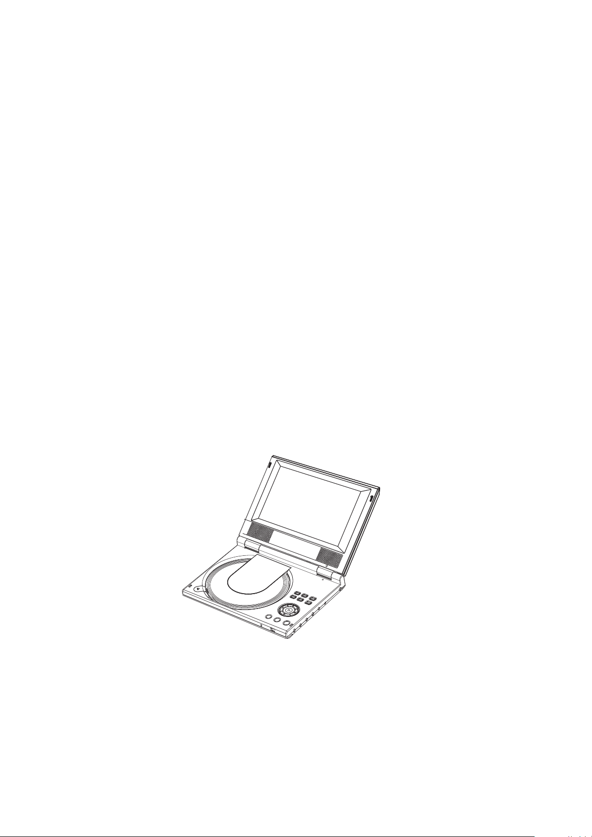
3.Control Button Locations and Explanations
2
1
2
3
4
5
6
7
8
9
10
1
Color TFT LCD
2
Speakers
3
OPEN/CLOSE button
4
PREV button / LEFT direction arrow
5
PAUSE button / DOWN
direction arrow
6
Vol-
Adjust the volume of headphone an
d speaker.
7
Vol+
Adjust the volume of headphone
and speaker.
8
Power indicator
9
IR sensor
10
Panel/Switch Button
19
18
17
16
15
14
13
12
11
Press once to switch to Direction
Buttons function
Press twice to switch to Virtual
Keyboard function
11
PLAY button / SELECT
button
12
NEXT button / RIGHT
direction arrow
13
STOP button / UP direction
arrow
14
SET button
15
PICTURE button
16
DVD/AUXIN button
17
POWER button
18
MENU button
19
Browser Button
Page 5
Control Button Locations and Explanations(Continued)
3
Page 6
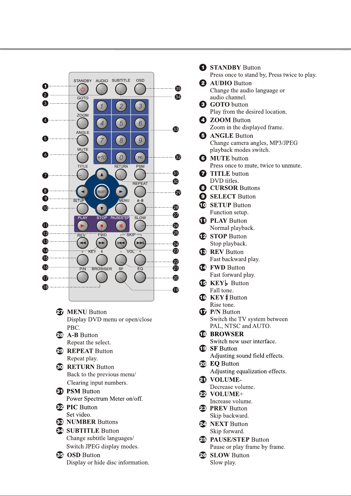
The laser diode in the traverse unit (optical pickup)may brake down due to static electricity of clothes or human
body. Use due caution to electrostatic breakdown when servicing and handling the laser diode.
Some devices such as the DVD player use the optical pickup(laser diode)and the optical pickup will be damaged
by static electricity in the working environment.Proceed servicing works under the working environment where
1. Put a conductive material(sheet)or iron sheet on the area where the optical pickup is placed,and ground the
3. The flexible cable may be cut off if an excessive force is applied to it.Use caution when handling the cable.
4
4.PREVENTION OF STATIC ELECTRICITY DISCHARGE
4.1.Grounding for electrostatic breakdown prevention
grounding works is completed.
4.1.1. Worktable grounding
sheet.
4.1.2.Human body grounding
1 Use the anti-static wrist strap to discharge the static electricity from your body.
safety_3 (1577x409x2 tiff)
4.1.3.Handling of optical pickup
1. To keep the good quality of the optical pickup maintenance parts during transportation and before
installation, the both ends of the laser diode are short-circuited.After replacing the parts with new ones,
remove the short circuit according to the correct procedure. (See this Technical Guide).
2. Do not use a tester to check the laser diode for the optical pickup .Failure to do so willdamage the laser
diode due to the power supply in the tester.
4.2. Handling precautions for Traverse Unit (Optical Pickup)
1. Do not give a considerable shock to the traverse unit(optical pickup)as it has an extremely high-precise
structure.
2. When replacing the optical pickup, install the flexible cable and cut is short land with a nipper. See the
optical pickup replacement procedure in this Technical Guide. Before replacing the traverse unit, remove
the short pin for preventingstatic electricity and install a new unit.Connect the connector as short times as
possible.
4. The half-fixed resistor for laser power adjustment cannot be adjusted. Do not turn the resistor.
Page 7
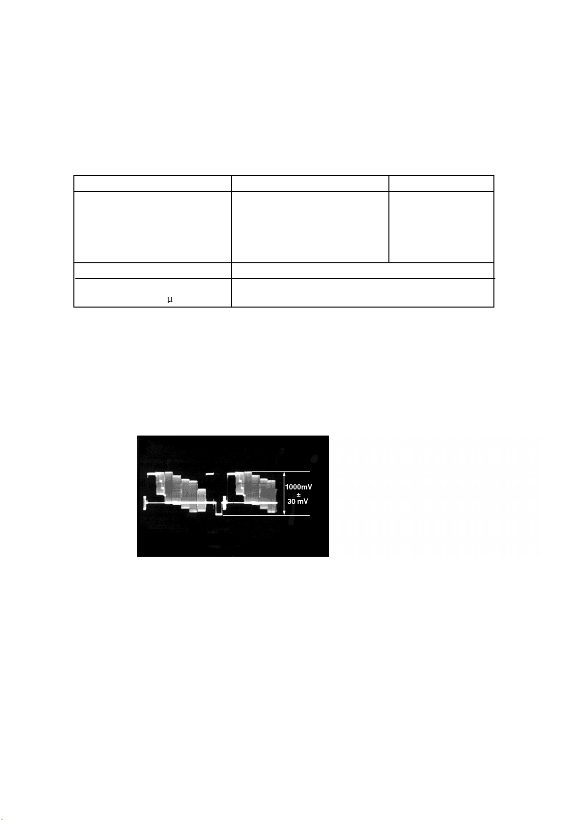
5.1. Video Output (Luminance Signal) Confirmation
5
5.Electrical Confirmation
DO this confirmation after replacing a P.C.B.
Measurement point
Video output terminal
Measuring equipment,tools
200mV/dir,10 sec/dir
Purpose:To maintain video signal output compatibility.
1.Connect the oscilloscope to the video output terminal and terminate at 75 ohms.
2.Confirm that luminance signal(Y+S)level is 1000mVp-p±30mV
PLAY(Title 46):DVDT-S15
PLAY(Title 12):DVDT-S01
Mode Disc
Color bar 75%
Confirmation value
1000mVp-p±30mV
DVDT-S15
or
DVDT-S01
Page 8
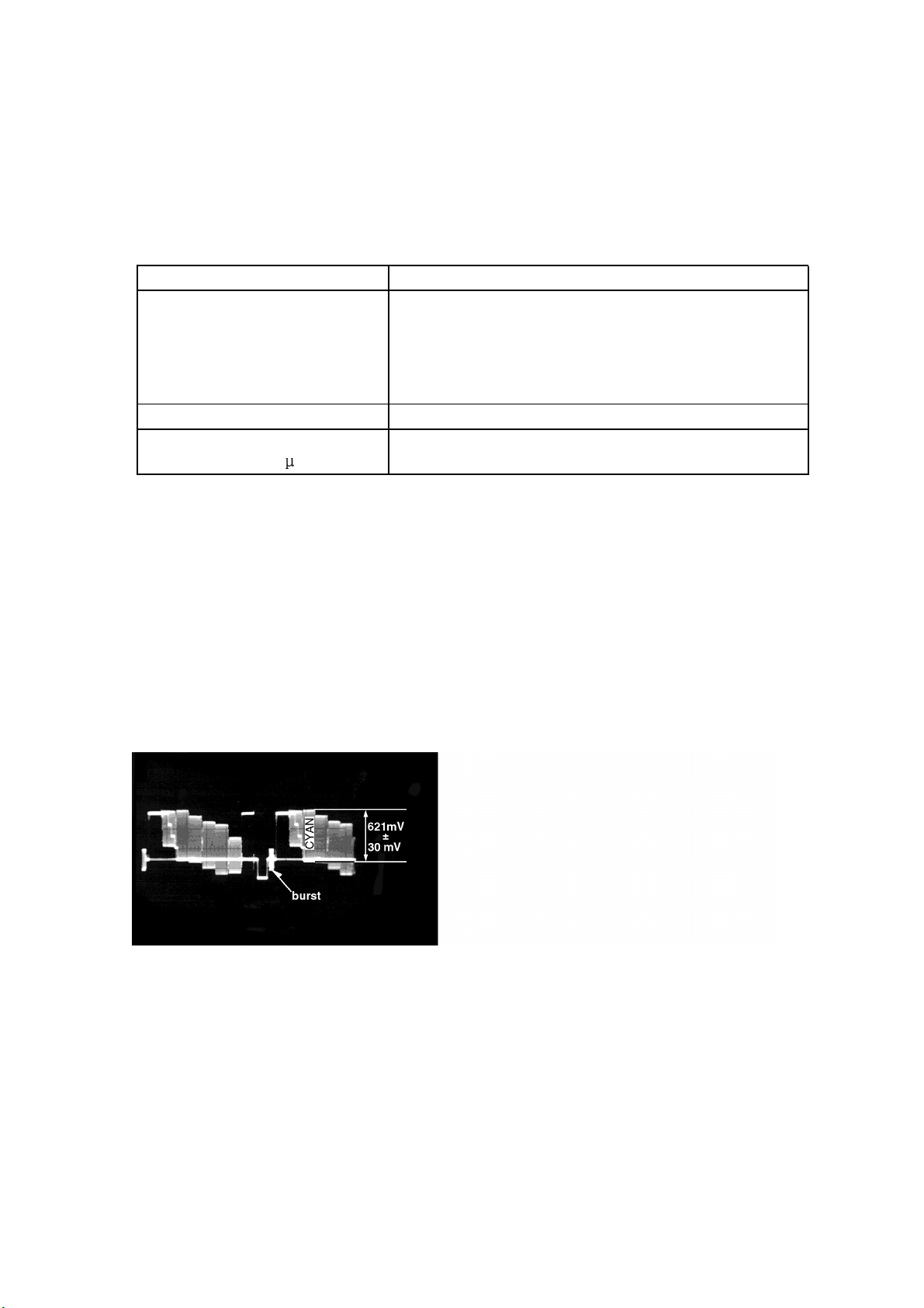
Do the confirmation after replacing P.C.B.
Screwdriver,Oscilloscope
5.2 Video Output(Chrominance Signal) Confirmation
6
Measurement point
Video output terminal
Measuring equipment,tools Confirmation value
200mV/dir,10 sec/dir
Purpose:To maintain video signal output compatibility.
1.Connect the oscilloscope to the video output terminal and terminate at 75 ohme.
2.Confirm that the chrominance signal(C)level is 621 mVp-p±30mV
PLAY(Title 46):DVDT-S15
PLAY(Title 12):DVDT-S01
Mode Disc
Color bar 75%
621mVp-p±30mV
DVDT-S15
or
DVDT-S01
Page 9
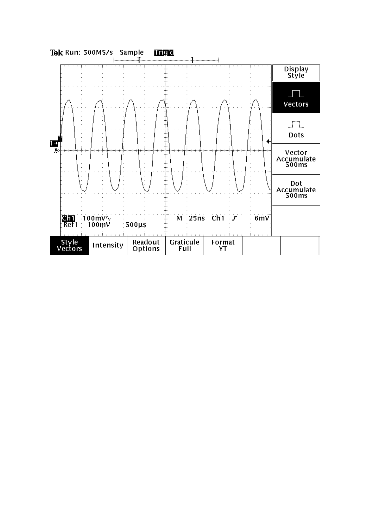
6.MPEG BOARD CHECK WAVEFORM
6.1 27MHz WAVEFORM
7
Page 10
7.2 MT1389
8
MT1389
Specifications are subject to change without notice
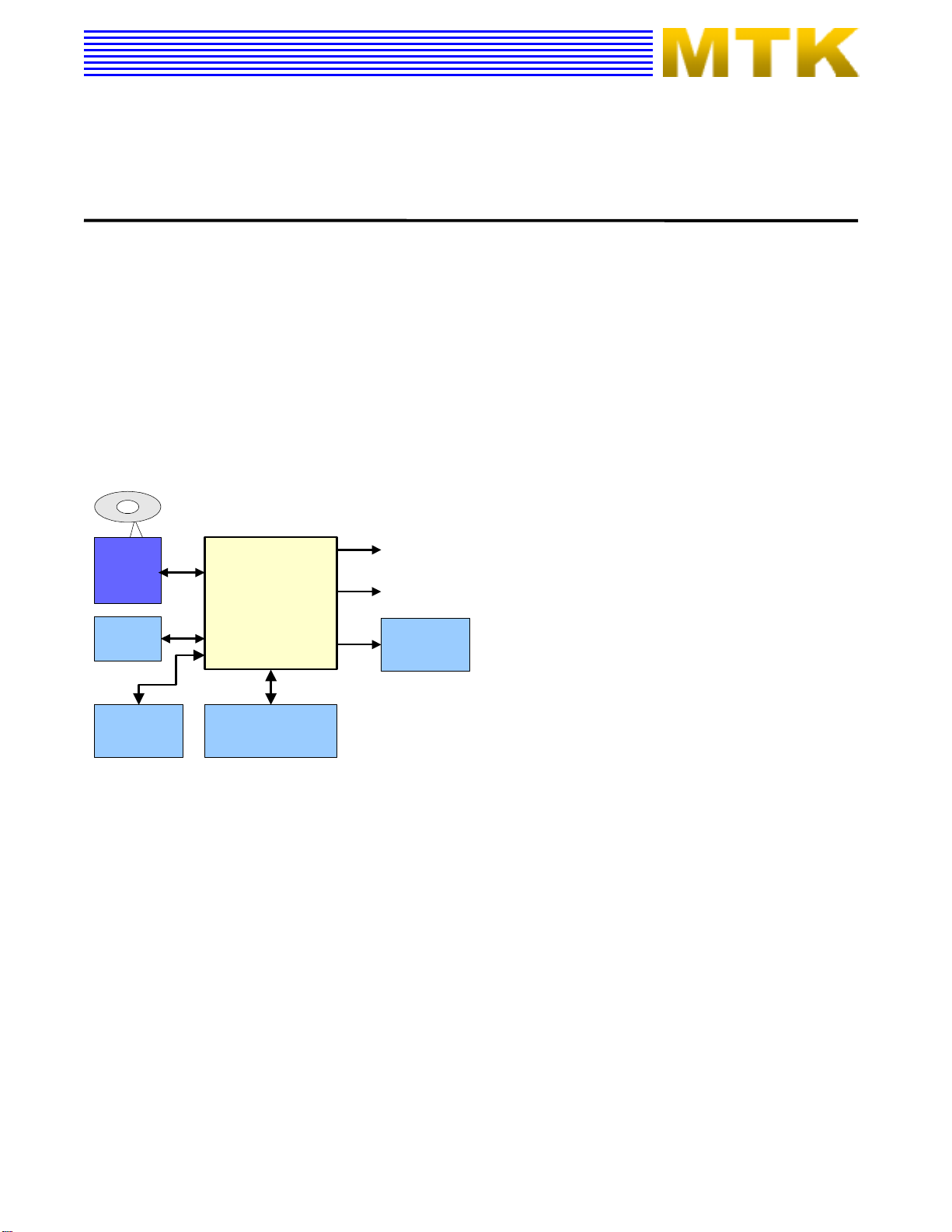
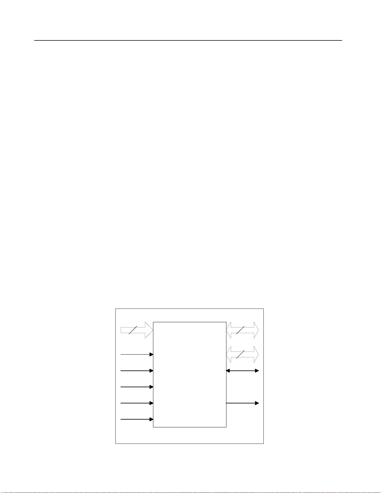
Progressive-Scan DVD Player SOC
MediaTek MT1389 is a DVD player system-on-chip (SOC) which incorporates advanced features like high
quality TV encoder and state-of-art de-interlace processing. The MT1389 enables consumer electronics
manufacturers to build high quality, cost-effective DVD players, portable DVD players or any other home
entertainment audio/video devices.
rd
Based on MediaTek’s world-leading DVD player SOC architecture, the MT1389 is the 3
player SOC. It integrates the MediaTek 2
decoder.
The progressive scan of the MT1389 utilized a proprietary advanced motion-adaptive de-interlace algorithm to
achieve the best movie/video playback. It can easily detect 3:2/2:2 pull down source and restore the correct
original pictures. It also supports a patent-pending edge-preserving algorithm to remove the saw-tooth effect.
nd
generation front-end analog RF amplifier and the Servo/MPEG AV
generation of the DVD
Key Features
RF/Servo/MPEG Integration
High Performance Audio Processor
Motion-Adaptive, Edge-Preserving De-interlace
108MHz/12-bit, 6 CH TV Encoder
DVD
PUH
Module
CVBS, Y/C,
Component
SDPIF
MT1389L
Applications
FLASH
Front-panel
Remote
DRAM
Audio DAC
Standard DVD Players
Portable DVD Players
DVD Player System Diagram Using MT1389
Page 11

9
PRELIMINARY, SUBJECT TO CHANGE WITHOUT NOTICE MTK CONFIDENTIAL, NO DISCLOSURE
MT1389
General Feature List
1024-bytes on-chip RAM
Super Integration DVD player single chip
High performance analog RF amplifier
Servo controller and data channel processing
MPEG-1/MPEG-2/JPEG video
Dolby AC-3/DTS/DVD-Audio
Unified memory architecture
Versatile video scaling & quality
enhancement
OSD & Sub-picture
2-D graphic engine
Built-in clock generator
Built-in high quality TV encoder
Built-in progressive video processor
Audio effect post-processor
Audio input port
Up to 4M bytes FLASH-programming
interface
Supports 5/3.3-Volt. FLASH interface
Supports power-down mode
Supports additional serial port
DVD-ROM/CD-ROM Decoding Logic
High-speed ECC logic capable of correcting
one error per each P-codeword or
Q-codeword
Automatic sector Mode and Form detection
Automatic sector Header verification
Decoder Error Notification Interrupt that
signals various decoder errors
Provide error correction acceleration
High Performance Analog RF Amplifier
Programmable fc
Dual automatic laser power control
Defect and blank detection
RF level signal generator
Speed Performance on Servo/Channel Decoding
DVD-ROM up to 4XS
CD-ROM up to 24XS
Channel Data Processor
Digital data slicer for small jitter capability
Built-in high performance data PLL for
channel data demodulation
EFM/EFM+ data demodulation
Enhanced channel data frame sync protection
& DVD-ROM sector sync protection
Servo Control and Spindle Motor Control
Programmable frequency error gain and
phase error gain of spindle PLL to control
spindle motor on CLV and CAV mode
Built-in ADCs and DACs for digital servo
control
Provide 2 general PWM
Tray control can be PWM output or digital
output
Embedded Micro controller
Built-in 8032 micro controller
Built-in internal 373 and 8-bit programmable
lower address port
Buffer Memory Controller
Supports 16Mb/32Mb/64Mb/128Mb SDRAM
Supports 16-bit SDRAM data bus
Provide the self-refresh mode SDRAM
Block-based sector addressing
Support 3.3 Volt. DRAM Interface
Video Decode
Decodes MPEG1 video and MPEG2 main level,
main profile video (720/480 and 720x576)
Smooth digest view function with I, P and B
picture decoding
Baseline, extended-sequential and
progressive JPEG image decoding
Support CD-G titles
Video/OSD/SPU/HLI Processor
Arbitrary ratio vertical/horizontal scaling of
video, from 0.25X to 256X
65535/256/16/4/2-color bitmap format OSD,
256/16 color RLC format OSD
Automatic scrolling of OSD image
Slide show transition as DVD-Audio
Specification
2-D Graphic Engine
Support decode Text and Bitmap
Support line, rectangle and gradient fill
Support bitblt
Chroma key copy operation
Clip mask
Page 12

10
PRELIMINARY, SUBJECT TO CHANGE WITHOUT NOTICE MTK CONFIDENTIAL, NO DISCLOSURE
MT1389
Audio Effect Processing
Dolby Digital (AC-3)/EX decoding
DTS/DTS-ES decoding
MLP decoding for DVD-Audio
MPEG-1 layer 1/layer 2 audio decoding
MPEG-2 layer1/layer2 2-channel audio
High Definition Compatible Digital (HDCD)
Windows Media Audio (WMA)
Advanced Audio Coding (AAC)
Dolby ProLogic II
Concurrent multi-channel and downmix out
IEC 60958/61937 output
- PCM / bit stream / mute mode
- Custom IEC latency up to 2 frames
Pink noise and white noise generator
Karaoke functions
- Microphone echo
- Microphone tone control
- Vocal mute/vocal assistant
- Key shift up to +/- 8 keys
- Chorus/Flanger/Harmony/Reverb
Channel equalizer
3D surround processing include virtual
surround and speaker separation
TV Encoder
Six 108MHz/12bit DACs
Support NTSC, PAL-BDGHINM, PAL-60
Support 525p, 625p progressive TV format
Automatically turn off unconnected channels
Support PC monitor (VGA)
Support Macrovision 7.1 L1, Macrovision
525P and 625P
CGMS-A/WSS
Closed Caption
Progressive Output
Automatic detect film or video source
3:2 pull down source detection
Advanced Motion adaptive de-interlace
Edge Preserving
Minimum external memory requirement
Audio Input
Line-in/SPDIF-in for versatile audio
processing
Outline
256-pin LQFP package
3.3/1.8-Volt. Dual operating voltages
Page 13
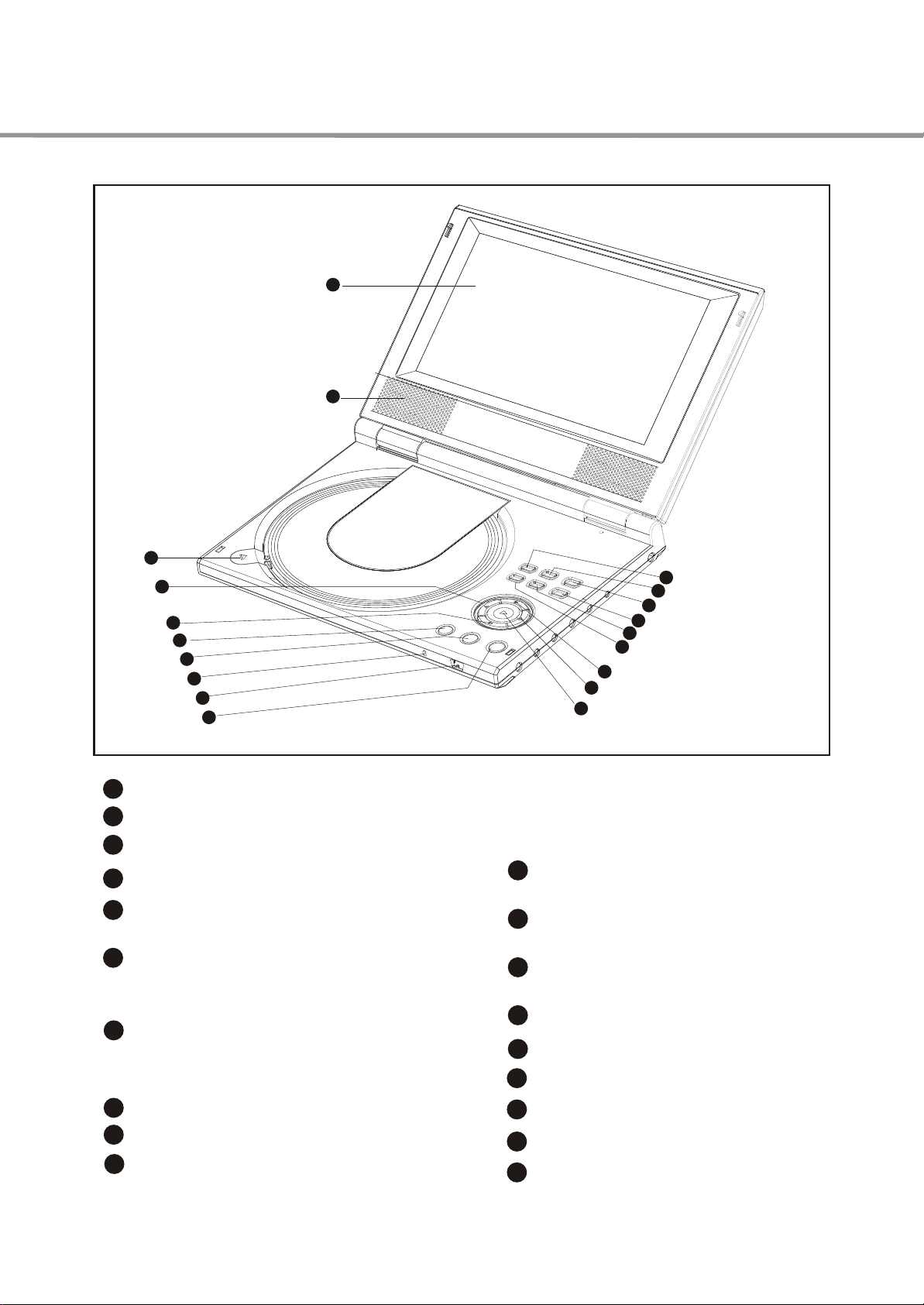
KEY FEATURES
IC BLOCK DIAGRAM & DESCRIPTION
11
7.3 U214 HY29F800
n 5 Volt Read, Program, and Erase
– Minimizes system-level power requirements
n High Performance
– Access times as fast as 55 ns
n Low Power Consumption
– 20 mA typical active read current in byte
mode, 28 mA typical in word mode
– 35 mA typical program/erase current
– 5 µA maximum CMOS standby current
n Compatible with JEDEC Standards
– Package, pinout and command-set
compatible with the single-supply Flash
device standard
– Provides superior inadvertent write
protection
n Sector Erase Architecture
– Boot sector architecture with top and
bottom boot block options available
– One 16 Kbyte, two 8 Kbyte, one 32 Kbyte
and fifteen 64 Kbyte sectors in byte mode
– One 8 Kword, two 4 Kword, one 16 Kword
and fifteen 32 Kword sectors in word mode
– A command can erase any combination of
sectors
– Supports full chip erase
n Erase Suspend/Resume
– Temporarily suspends a sector erase
operation to allow data to be read from, or
programmed into, any sector not being
erased
n Sector Protection
– Any combination of sectors may be
locked to prevent program or erase
operations within those sectors
n Temporary Sector Unprotect
– Allows changes in locked sectors
(requires high voltage on RESET# pin)
n Internal Erase Algorithm
– Automatically erases a sector, any
combination of sectors, or the entire chip
n Internal Programming Algorithm
– Automatically programs and verifies data
at a specified address
n Fast Program and Erase Times
– Byte programming time: 7 µs typical
– Sector erase time: 1.0 sec typical
– Chip erase time: 19 sec typical
n Data# Polling and Toggle Status Bits
– Provide software confirmation of
completion of program or erase
operations
n Ready/Busy# Output (RY/BY#)
– Provides hardware confirmation of
completion of program and erase
operations
n Minimum 100,000 Program/Erase Cycles
n Space Efficient Packaging
– Available in industry-standard 44-pin
PSOP and 48-pin TSOP and reverse
TSOP packages
19
A[18:0]
CE#
OE#
WE#
RESET#
BYTE#
8
DQ[7:0]
7
DQ[14:8]
DQ[15]/A-1
RY/BY#
Page 14

BLOCK DIAGRAM
IC BLOCK DIAGRAM & DESCRIPTION
12
DQ[15:0]
A[18:0], A-1
DQ[15:0]
WE#
CE#
OE#
BYTE#
RESET#
RY/BY#
STATE
CONTROL
COMMAND
REGISTER
PROGRAM
VOLTAGE
GENERATOR
VCC DETECTOR TIMER
ERASE VOLTAGE
GENERATOR AND
SECTOR SWITCHES
A[18:0], A-1
ADDRESS LATCH
I/O CONTROL
Y-DECODER
X-DECODER
I/O BUFFERS
DATA LATCH
Y-GATING
8 Mb FLASH
MEMORY
ARRAY
Page 15

PIN CONFIGURATIONS
IC BLOCK DIAGRAM & DESCRIPTION
13
RY/BY#
A18
A17
A7
A6
A5
A4
A3
A2
A1910
A0
CE#1112
V
SS
OE#1314
DQ0
DQ81516
DQ1
DQ91718
DQ2
DQ101920
DQ3
DQ112122
1
2
3
4
5
6
7
8
PSOP44
44
43
42
41
40
39
38
37
36
35
34
33
32
31
30
29
28
27
26
25
24
23
RESET#
WE#
A8
A9
A10
A11
A12
A13
A14
A15
A16
BYTE#
V
SS
DQ15/A-1
DQ7
DQ14
DQ6
DQ13
DQ5
DQ12
DQ4
V
CC
A15
A14
A13
A12
A11
A10
A9
A8
NC
NC910
WE#
RESET#1112
NC
NC1314
RY/BY#
A181516
A17
A71718
A6
A51920
A4
A32122
A2
A12324
A16
BYTE#
V
SS
DQ15/A-1
DQ7
DQ14
DQ6
DQ13
DQ5
DQ12
DQ4
V
CC
DQ11
DQ3
DQ10
DQ2
DQ9
DQ1
DQ8
DQ0
OE#
V
SS
CE#
A0
10
11
12
13
14
15
16
17
18
19
20
21
22
23
24
A16
1
2
3
4
5
6
7
8
Standard
TSOP48
1
2
3
4
5
6
7
8
9
Reverse
TSOP48
48
47
46
45
44
43
42
41
40
39
38
37
36
35
34
33
32
31
30
29
28
27
26
25
48
47
46
45
44
43
42
41
40
39
38
37
36
35
34
33
32
31
30
29
28
27
26
25
BYTE#
V
SS
DQ15/A-1
DQ7
DQ14
DQ6
DQ13
DQ5
DQ12
DQ4
V
CC
DQ11
DQ3
DQ10
DQ2
DQ9
DQ1
DQ8
DQ0
OE#
V
SS
CE#
A0
A15
A14
A13
A12
A11
A10
A9
A8
NC
NC
WE#
RESET#
NC
NC
RY/BY#
A18
A17
A7
A6
A5
A4
A3
A2
A1
Page 16

HY57V641620HG
14
7.4 HY57V641620HG
4 Banks x 1M x 16Bit Synchronous DRAM
DESCRIPTION
The Hyundai HY57V641620HG is a 67,108,864-bit CMOS Synchronous DRAM, ideally suited for the main memory applications which
require large memory density and high bandwidth. HY57V641620HG is organized as 4banks of 1,048,576x16.
HY57V641620HG is offering fully synchronous operation referenced to a positive edge of the clock. All inputs and outputs are synchronized with the rising edge of the clock input. The data paths are internally pipelined to achieve very high bandwidth. All input and output
voltage levels are compatible with LVTTL.
Programmable options include the length of pipeline (Read latency of 2 or 3), the number of consecutive read or write cycles initiated
by a single control command (Burst length of 1,2,4,8 or Full page), and the burst count sequence(sequential or interleave). A burst of
read or write cycles in progress can be terminated by a burst terminate command or can be interrupted and replaced by a new burst
read or write command on any cycle. (This pipelined design is not restricted by a `2N` rule.)
FEATURES
• Single 3.3±0.3V power supply
• All device pins are compatible with LVTTL interface
• JEDEC standard 400mil 54pin TSOP-II with 0.8mm
of pin pitch
• All inputs and outputs referenced to positive edge of
system clock
• Data mask function by UDQM or LDQM
• Internal four banks operation
Note)
• Auto refresh and self refresh
• 4096 refresh cycles / 64ms
• Programmable Burst Length and Burst Type
- 1, 2, 4, 8 or Full page for Sequential Burst
- 1, 2, 4 or 8 for Interleave Burst
• Programmable CAS Latency ; 2, 3 Clocks
.
Page 17

PIN CONFIGURATION
15
HY57V641620HG
VDD
DQ0
VDDQ
DQ1
DQ2
VSSQ
DQ3
DQ4
VDDQ
DQ5
DQ6
VSSQ
DQ7
DD
V
LDQM
/WE
/CAS
/RAS
/CS
BA0
BA1
A10/AP
A0
A1
A2
A3
DD
V
1
2
3
4
5
6
7
8
9
10
11
12
13
14
15
16
17
18
19
20
21
22
23
24
25
26
27
54pin TSOP II
400mil x 875mil
0.8mm pin pitch
VSS
54
DQ15
53
VSSQ
52
DQ14
51
DQ13
50
VDDQ
49
DQ12
48
DQ11
47
VSSQ
46
DQ10
45
DQ9
44
VDDQ
43
DQ8
42
SS
V
41
NC
40
UDQM
39
CLK
38
CKE
37
NC
36
A11
35
A9
34
A8
33
A7
32
A6
31
A5
30
A4
29
SS
V
28
PIN DESCRIPTION
PIN PIN NAME DESCRIPTION
CLK Clock
CKE Clock Enable
CS Chip Select Enables or disables all inputs except CLK, CKE and DQM
BA0,BA1 Bank Address
A0 ~ A11 Address
Row Address Strobe,
RAS, CAS, WE
LDQM, UDQM Data Input/Output Mask Controls output buffers in read mode and masks input data in write mode
DQ0 ~ DQ15 Data Input/Output Multiplexed data input / output pin
VDD/VSS Power Supply/Ground Power supply for internal circuits and input buffers
VDDQ/VSSQ Data Output Power/Ground Power supply for output buffers
NC No Connection No connection
Column Address Strobe,
Write Enable
The system clock input. All other inputs are registered to the SDRAM on the
rising edge of CLK
Controls internal clock signal and when deactivated, the SDRAM will be one
of the states among power down, suspend or self refresh
Selects bank to be activated during RAS activity
Selects bank to be read/written during CAS activity
Row Address : RA0 ~ RA11, Column Address : CA0 ~ CA7
Auto-precharge flag : A10
RAS, CAS and WE define the operation
Refer function truth table for details
Page 18

FUNCTIONAL BLOCK DIAGRAM
I/O Buffer & Logic
16
1Mbit x 4banks x 16 I/O Synchronous DRAM
HY57V641620HG
Self refresh logic
& timer
CLK
CKE
CS
RAS
CAS
WE
UDQM
LDQM
Row active
State Machine
refresh
Column
Active
Internal Row
counter
Row
Pre
Decoders
Column
Pre
Decoders
1Mx16 Bank 3
X decoders
1Mx16 Bank 2
X decoders
X decoders
1Mx16 Bank 1
1Mx16 Bank 0
X decoders
Memory
Y decoders
Cell
Array
Sense AMP & I/O Gate
DQ0
DQ1
DQ14
DQ15
Bank Select
A0
A1
A11
BA0
BA1
Address buffers
Address
Registers
Mode Registers
Column Add
Counter
Burst
Counter
CAS Latency
Data Out Control
Pipe Line Control
Page 19

F
8.SCHEMATIC & P.C.B WIRING DIAGRAM
DECODE BOARD
17
E
123
C123 151
C112
104
FMSO
R123 20K
R106
10K
TRSO
V1P4
STBY
28
U104
BA5954
VINSL+
VINSL-
VINFC
VOSL
CF12CF2
4
5
6
3
1
V1P4
FOSO
R124 20K
C124
151
XS15
SL-
SL+
MO_VCC
R126
47R
104
104
H-
R127
104
47R
HV+
HV-
HW+
HW-
15
30
BA6849/6869
G2
GND
CNF
BR
G1
HSOP28/SMD
16
17
18
29
8
R131
C116
104
R
C117
104
47uF/16V
TC109
PREGND22VINLD23CTK224CTK125VINTK26BIAS27STBY
VINFFC
HU+H+UVW
FR20SB
A
1
XS101
30
AVCC
23 4
R101
100K
CE
V101
3904-S
B
R103
10K
R104
10K
AVCC
IOA
R140
0R
DQS0
AT24C16X4050
U101
8
DV33
C103
104
R109
680R
R110
680R
5
VR-DVD
V104
104
B
VR-CD
V20
DVDRFIP
SPLRCK
L104
L102
L105
L106
L103
C104
L114
L115
104
FBSMT
FBSMT
FBSMT
FBSMT
FBSMT
CCCBSUBB
SUBC
R111
4.7R
LDO-AV33
TC103
47uF/16V
LDO1
FBSMT
L119
AV33
AVCC VCC
C106
104
10uH 2012
L107
C107
104
C108
104
+9V
A5V
C102
DV33
FBSMT
FBSMT
C E
EEPROM
102(DNS)
C118
C119
102(DNS)
L101
L116
L113
L112
L111
FCM2012-120T2A
FBSMT
FBSMT
FBSMT
FBSMT
D
AVCC
SUBD
SUBAAIOA
C105
104
100uF/16V
TC102
2SK3018-S
V102
2SK3018-S
V103
B
R102
100K
4
DC/NC1RST_/NC2WP/RST_3VSS
RST/WP
VCC
SDA
SCL
7
5
6
SDA
SCL
4.7R
XS103
翻盖检测关闭开关
1
TRIN
R105
10K
R137
15K
R139
47K
5
电池电压检测电路
4 8
LM393
DET 6.0V AND LOWBAT WARNING
C
XS30
2341568910711121415161317182021221923242627282529
R112
DV33
6
7
33R
LOWBAT_DE T
T-
T+
F+
47uF/16V
TC104
LDO-AV33
R136
470R
4 8
U105B
R134
4.7K
R143
MDI1
LD-CD
LD-DVD
AVCC
F-
L118
L117
10uH 2012
10uH 2012
2SB1132-S
V105
2SB1132-S
LDO2
R135
20K
R138
47K
3
2
U105A
LM393
1
R133
4.7K
DET 5.7V AND SYSTEM OFF
R142
33R
POWEROFF_DET
D
TC105
47uF/16V
MO_VCC
C126
104
104
C110
C111
104
SL-
21
PVCC1
VOSL-
PGND
VCC
7
10
9
11
8
R107
10K
SP+
HW+
HV-
HV+
HU-
WVU
C113
C114
R1290RR1280RR130
C115
HU-
HU+
0R
A32A24A17RNF
H1+9H1-10H2+11H2-12H3+13H3-14VH
ECR
FG
EC
PS
21
23
24
22
FG
STBY
V1P4
DMSO
SL+
VOFC-
VO2+
12
13
SP-
234156891071112141513
LIMITH-HW-
VCC25VM1
VM2
26
VOTK+15VOTK-16VOLD+17VOLD-18PGND19VNFTK20PVCC2
GND
GND
VOFC+
22uF/16V
TC101
V1P4
R116
1R
R117
1R
T-
T+
29
30
F+
14
XS104
28
27
F-
MO_VCC
L120
10uH 2012
R118
1R
R119
1R
U103
VCC
XS02
2
R120
1R
R121
1R
R122
1R
C109
104
TC108
47uF/16V
MO_VCC
R144
10K
TC107
100uF/16V
R141
100K(DNS)
R145
33R
URST#
DV33
VD101
1N4148
U106
IMP8009(DNS)
3
VCC
2
RST
1
GND
C125
104(DNS)
XS102
CPU5V
IR
R114 100R
R132
150R
D
C121
47pF(DNS)
R115
4.7K(DNS)
TC106
47uF/10V
C122 103
CPU5V
R113
10R
1
U102
HS0038B
GND2VCC3OUT
IR遥控 输入电路
C
B
XS04
C120
47pF
234
1
1 2
L110
L108
L109
C101
27pF
10uH 2012
FBSMT
FBSMT
POWER
VSDA
DV33
6
A
Page 20

A
DECODE BOARD
18
DQ0
DQ1
DQ2
DQ4
DQ5
DQ6
DQ7
XI
XO
C264
33pF
R227 0R
R204 100K
R226 0R
X201
6
27MHz
33pF
C263
DMA5
DMA4
R255
0R(DNS)
R256
0R(DNS)
R257
DMA5#
DMA4#
DMA10# DMA10
5
L202
FBSMT
DACVDD3 DV33
Y1
Y2
Y3
R210 (DNS)
R211 (DNS)
R212 (DNS)
Y4
Y5
Y6
1K
SPLRCK
R214
(DNS)
(DNS)
(DNS)
(DNS)
89V33
ALRCK
ABCK
ACLK
R209
R208
R207
R206
ASDAT0
MUTE_DAC
V18
RST#
AMDAT
ASPDIF
R205
(DNS)
XO
RFV18
XI
JITFO
JITFN
C261 0.47uF
PLLVDD3
0.047uF
TC204
10uF/16V
C260
0.047uF
C259
ADCVDD3
C251 1uF
20pF
C258
C257
V1P4
23 4
C277
PLLVDD3
4.7R
L206
1
VREFP
VREFN
1000pF
RFVDD3
100K
R203
104
C211
0.033uF
C256
104
C210
104
C209
104
C208
R201
15K
C207
104
104
C250 1uF
C205
104
VREFN VREFP
TC201
47uF/16V
RFVDD3
ADCVDD3
C201
104
C202
104
FBSMT
FBSMT
L207
L208
L201
FBSMT
RFV33
DQ3
DQ02DQ14DQ25DQ37DQ48DQ510DQ611DQ713DQ842DQ9
A023A124A225A326A429A530A631A732A833A934A10/AP22A1135BA0/A1320BA1/A1221CLK38CKE37/CS19/RAS18/CAS17/WE16DQML15DQMH39NC36NC40VSS54VSS41VSS
U202
DMA0#
DMA1#
DMA2#
DMA3#
DMA4#
DMA5#
DMA6#
DMA7#
JITFNJITFO
1000pF
C262
0R(DNS)
C214
C213
C212
AVDD3
C203
104
DMA11
R254
BA0
BA1
R216 750K
560R
TC205
Y0
10uF/16V
104
104
104
193
194
195
196
197
198
199
200
201
202
203
204
205
206
207
208
209
210
211
212
213
214
215
216
217
218
219
220
221
222
223
224
225
226
227
228
229
230
231
232
233
234
235
236
237
238
239
240
241
242
243
244
245
246
247
248
249
250
251
252
253
254
255
256
C206
104
RFSVDD3
FBSMT
L209
89V33 V18
ABCK
ACLK
DVSS
DVSS
SPDIF
XTALI
JITFO
JITFN
LPFIP
LPFIN
LPFOP
CEQP
CEQN
OSP
OSN
RFGC
IREF
C249 1uF
BAD
C204
104
YUV1/Y
YUV2/C
YUV4/G
YUV5/B
YUV6/R
DVDD3
SPMCLK
SPDATA
SPLRCK
DVDD3
ALRCK
DVDD18
XTALO
PLLVSS
LPFON
S_VCM
ADCVSS
S_VREFP
S_VREFN
RFVDD3
RFRPDC
RFRPAC
HRFZC
CRTPLP
RFGND
AVDD3
C252 1uF
C269 104
R236
FS
191
192
190
FS
DACVSSC
YUV0/CIN
DACVDDB
DACVSSB
YUV3/CVBS
DACVDDA
DACVSSA
VSYNC/V_ADIN1
YUV7/ASDATA5
HSYNC/V_ADIN2
SPBCK/ASDATA5
ASDATA0
ASDATA1
ASDATA2
ASDATA3
ASDATA4
MC_DATA
RFGND18
RFVDD18
IDACEXLP
PLLVDD3
ADCVDD3
DVDA
DVDB3DVDC4DVDD
AGND
2
1
C253 1uF
C254 1uF
CCC
L210
FBSMT
V18 RFV18
A
B
SD33
DQ8
DQ9
DQ10
DQ11
DQ12
DQ13
DQ14
44
DQ1045DQ1147DQ1248DQ1350DQ1451DQ15
DMA8#
DMA9#
DMA10#
MA11
#BA0
#BA1
R224
33R
33R
1 2
R223
33R
ASTB#
NFC#
0R
R261
NFC
ASTB
0R(DNS)
R252 0R
R258
188
187
186
185
184
183
189
RD16
RD17
RD18
RD19
RD20
VREF
DACVDDC
DVDRFIP6DVDRFIN7MA8MB9MC10MD11SA12SB13SC14SD15CDFON16CDFOP17TNI18TPI19MDI120MDI221LDO222LDO1
5
CCC
C255 1uF
DAB
DVDRFIP
104
C215
SD33
DQ15
27
53
VCC1VCC14VCC
DCS#
DRAS#
SDCLK
SDCKE
DCAS#
DWE#
876
5
33R
123
4
R219
R218 33RDCLK
RN201
CS#
RAS#
CAS#
WE#
DCKE
0R
MS_BS
0R
MS_SDIO
R259
R262
SD_CDN
SD_WP
MS_INS
POWEROFF_DET
LOWBAT_DE T
NFC#
ASTB#
179
178
181
180
177
176
182
RD21
RD22
RD23
RD24
RD25
DQM2
DQM3
DVDD3
SUBA
SUBB
SUBC
SUBD
TN1
C268
15P
C267
15P
C266
15P
C265
15P
RFV33
104
C216
TC206
L203
FBSMT
220uF/16V
DV33
B
VCCQ3VCCQ9VCCQ43VCCQ
DQM0
DQM1
33R
33R
RN204
0R
R260
MS_CLK
174
173
175
RD26
DVSS
TP1
MDI1
MDI2
0R
R230
C218
DMA0#
876
123
DMA0
DVDD18
C
TC202
49
52
VSSQ6VSSQ12VSSQ46VSSQ
28
DMA1#
DMA2#
DMA3#
DMA6#
DMA7#
DMA8#
5
876
4
123
DMA1
DMA2
DMA3
DMA6
DMA7
DMA8
DMA4
SD_CLK
SD_CMD
SD_D0
VOL-DATA
VOL-CLOCK
172
171
170
169
168
166
167
RA4
RD27
RD28
RD29
RD30
DVDD3
RD31/ASDATA5
V2REFO28SGND27VREFO30V2029TEO32FEO
RFLVL/RFO N26CSO/RFOP
SVDD3
23
25
24
RFOP
RFON
104
R229 0R(DNS)
LDO2
LDO1
V2P8
RFSVDD3
C225
C224
C223
SDRAM 64M
C222
C221
C220
SD33
C219
DMA9#
5
FBSMT
33R
L204
4
DV33
RN205
DMA9
DMA9
DMA8
DMA7
DMA6
DMA5
165
164
162
160
159
163
161
RA5
RA6
RA7
RA8
RA9
DVSS
DVSS
MT1389
U201
TEZISLV33OP_OUT34OP_INN35OP_INP36FOO42TRO41USBM
31
FEO
TEO
TEZISLV
OPO
OP-
V20
V1P4
C217 104
R228
0R(DNS)
V2P8
47uF/16V
104
104
104
104
104
104
104
DMA11
DCKE
DCLK
158
157
156
CKE
RA11
37
DMO
FMO
OP+
15K
10K
R240
DMSO
FMSO
TC207
T47uF/16V
C226
104
C
U203 8/16/32M_FLASH(TSOP)
UPA[20..0]
UPD[15..0]
A20
DMA2
DMA3
DCLKB
152
151
150
155
154
153
RA3
RCLK
DVDD3
RCLKB
DVDD18
RVREF/V_ADIN3
USB_VSS
TROPENPWM39PWMOUT1/V_ADIN940USB_VDD3
FMO38DMO
43
TRO
FOO
TROPEN
USBP
18K
20K
C275
R243
R244
R202
C274
C273
C272
TRSO
FOSO
D
A17
GNDA0AD7
AD14
AD6
AD13
48
41
42
44
47
46
45
Vss
A16
DQ6
DQ7
DQ1443DQ13
BYTE
DQ15/A-1
A12
A9
A151A142A133A115A106A88A199WE11RESET
4
7
A15
A14
A13
A12
A11
A10
A9
A16
0R(DNS)
VD
CS#
BA0
BA1
DMA0
DMA1
DMA10
146
142
149
147
145
143
148
144
RA2
RA1
RA0
BA1
BA0
RCS
RA10
DVSS
DVSS
45
46
USBVDDFGTROUT
USBM
330pF
103
V1P4
52
51
TRIN
TRCLOSEA2A3A4A5A6A7A8A18
STBY
V18
FBSMT
104
C227
L211
89V33
DVDD18
V1P4
USBP44FG/V_ADIN847TDI/V_ADIN448TMS/V_ADIN549TCK/V_ADI N650TDO/V_ADIN7
330pF
153pF
D
AD5
DQ540DQ4
AA20
141
DVDD3
IOA253IOA354IOA455IOA5
V20
AD12
AD4VDAD11
38
DQ1239DQ11
NC10NC
DWR#
AA21
R249
R248 0R(DNS) A21
R241 10K
R247 4.7K
R246 4.7K
R245 4.7K
R253 4.7K
RAS#
CAS#
140
139
RAS
CAS
37
36
Vcc
13
12
WE#
DQM1
137
138
RWE
56
DQM1
IOA657IOA7
AD3
AD10
34
35
DQ10
14
DQ8
LIMIT
135
136
RD8
DQS1
HIGHA0
59
58
TC209
T47uF/16V
C230
104
TC208
T47uF/16V
C228
104
E
AD2
AD9
AD1
AD8
AD0
DRD#
32
29
31
28
DQ830DQ9
DQ233DQ3
DQ0
DQ1
A619A1717RY/BY15A1816NC
A520A421A322A7
18
A19
A18A7A6A5A4A3A2
A8
R250
4.7K(DNS)
DQ9
DQ10
DQ11
DQ12
DQ13
129
132
131
130
133
134
RD9
RD10
RD11
DR12
DVSS
DVSS62APLLCAP
APLLVSS
IOA1860IOA19
63
64
61
A19
C276
R231 0R
F
GND
DCE#
A1
VCC
25
27
CE26A0
OE
Vss
L214
FBSMT
L215
FBSMT(DNS)
TC203
VD DV33
DV33
RD14
DVDD3
RD15
RD0
RD1
RD2
DVDD18
RD3
RD4
DVSS
RD5
RD6
DVSS
RD7
DQS0
DQM0
INT0
IR
PRST
ICE
DVDD3
UP3_5
UP3_4
UP3_1
UP3_0
UP1_7
UP1_6
UP1_5
UP1_4
UP1_3
UP1_2
DVDD18
URD
UWR
DVSS
IOA0
A17
AD7
ALE
IOA21/V_ADIN0
AD6
AD5
AD4
DVSS
AD3
AD2
AD1
AD0
DVDD3
IOOE
IOA1
IOCS
IOA20
HIGHA1
HIGHA2
DVDD3
HIGHA3
HIGHA4
HIGHA5
HIGHA6
HIGHA7
A16
IOWR
APLLVDD3
L205
33R
C236
104
C235
104
C234
104
C233
104
C232
104
C231
104
C229
104
47uF/16V
C248
104
CLOCKCLOCK#
876
5
RN203
33R(DNS)
123
4
CS## CS
DATA# DATA
STROBE# STROBE
R215
1K(DNS)
DQ14
128
127
DQ15
126
125
DQ0
DQ1
124
DQ2
123
122
DQ3
121
120
DQ4
119
118
DQ5
DQ6
117
116
DQ7
115
DQS0
114
113
DQM0
112
111
110
109
108
107
106
105
104
103
102
101
100
99
98
97
96
95
94
93
92
91
90
89
88
87
86
85
84
83
82
81
80
79
78
77
76
75
74
73
72
71
70
69
68
67
66
65
C246
TC210
22uF/16V
C244
104
C242
104
C240
104
DV33A
DV33A
AVDD3
L216
FBSMT
L212
FBSMT
R251 4.7K
URST#
TXD
RXD
STROBE#
DATA#
SDA
SCL
CS## AIN-DET
CLOCK#
V18
A0
A17
AD7
A21
AD6
AD5
AD4
AD3
AD2
AD1
AD0
PRD#
A1
PCE#
A20
A9
A10
A11
A12
A13
A14
A15
A16
PWR#
104
1
3
2
VSDA
IR
VD201
MMBD4148CA
DV33
C247
104
DV33
RXD
TXD
GND
R213
0R(DNS)
234
1
XS201
XS04(DNS)
DWR#
DCE#
DRD#
876
5
RN202
0R
123
4
PWR#
PCE#
PRD#
C245
104
C243
104
C241
104
C239
104
C238
104
V18
C237
104
123
F
A223A1
24
R242
10K
RD13
1500pF
89V33
L213
FBSMT
DV33
E
Page 21

A
DECODE BOARD
19
JK301
A-out
23415
6
6
C321
102
Lt
L301
FBSMT
LOUT
R318
5
R317 36K
4
R308
330R
CH-L
TC304
T10uF/16V
L
1
U305A
+8V
3
2
C319 68P
C317
R314
4.7K
R312
10K
C315
R310
11K
15K
ALIN
TC303
T10uF/16V
L331
A5V VCC1
3
LL
MUTECRST#
16
15
MUTEC
RST1SDA2SCLK3LRCK4MCLK5DIF16DIF07DEM0
U304 CS4340/1
TC302
T10uF/16V
A5V
2
GND
1
OUT
2
IN
3
U302 78L05
SDATA0
MUTE9V
GND
1
OUT
2
IN
3
U301
AN77L08M
MUTE9V +8V
C322
102
AGND
R320
100K
V301
2SC1815-Y
R319
1K
MUTE-1
4580
4 8
152
102
FCM2012-120T2A (DNS)
TC311
10uF/25V
C301
104
RR
13
12
14
VA
AGND
AOUTA
AOUTB
SBCLK
SLRCK
SACLK
TC301
100uF/16V
L326
R321
100K
V302
2SC1815-Y
R328
R327
1K
TC308
+8V
R316 36K
6
C320 68P
R315
4.7K
AGND
R313
10K
12
R311
11K
R309
15K
ARIN
TC307
TC306
T10uF/16V
C305
104
TC305
T10uF/16V
C304
104
9
10
11
VQ
FILT+
REF-GND
8
0R
R302
0R
R303
R304
0R
C303
104
AGND
C302
104
+8V
1
A
Rt
ROUT
CH-R
R
7
VCC1
A5V
FBSMT
5
C318
C316
T10uF/16V
AGND
U303
AGND
JK302
Ain
R330
421
3
1 2
T10uF/16V
ALIN
AIN-DET
TC316
C306
104
47K
5
4
ASDAT0 SDATA0
BL9V
BLGND
FBSMT
L305
9
1K
1K
R329
TC329
TC310 T10uF/16V
AGND
ARIN
47uF/10V
V304
AGND
R342
1K
MUTE9V
VCC1
MUTE9V
L308
10uH 2012
L325
FCM2012-120T2A
VIN
33R
DV33
GND
TC312
47uF/16V
CLOCK
DATA
GND
-10V
+15V
STROBE
FBSMT(DNS)
FBSMT
FBSMT
FBSMT(DNS)
FBSMT(DNS)
L320
L307
L306
L321
L322
23416785101112
R340
82K
82K
R368
TC309
+8V
330R
R326
39K
T10uF/16V
R322
U305B
4580
4 8
152
AGND
102
876
RN301
123
ACLK SACLK
ABCK SBCLK
ALRCK SLRCK
GND
1
OUT
2
IN
3
78L05
BL9V
+7.5V
STBTA
FBSMT
L304
L302 0R
XS301
XS12
B
C
JK301
OPTICAL
23415
6
AGND
C332
27pF
R346
33R
47uF/10V
DV33
ASPDIF
C307
104
MUTE9V
VD302
1N4148
TC315
47uF/16V
AGND
R345 150R
MUTE-1
V305
8550
R344
DNS
VD303
4.7V
8550
1K
R332
R331
MUTEC V303
TC317
47uF/10V
GND
VGND
1K
R367
L324 0R(DNS)
XS302
CS
C326
C325
C324
C323
TC314
FBSMT(DNS)
L323
TC313
AGND
V306
8050
1K
R341
R333
1K
8550
VD301
1N4148
1K
MUTE_DAC
C345
27PF
RSOUT-
LSOUT+
LSOUT-
C#
Y#
RSOUT+
VGND
NFC
FBSMT
FBSMT
FBSMT
FBSMT
FBSMT
FBSMT
L313
L312
L309
L310
L314
L311
L303 0R
2341568
7
DNS
DNS
DNS
DNS
47uF/16V
47uF/16V
C
JK304
Vin
1
3
2
11
10
104
TC320
10uF/10V
VD304
MMBD4148SE
2
V5V
1
VGND
AGND
R361
V5V
R343
1K
AGND
V5V
TC319
47uF/10V
L327
FBSMT
47uF/10V
VCC1
TC318
C331
27pF
C330
27pF
XS08
TO TFT-LCD
VDD
R347
C308
C#
Y#
2
V5V
3
1
75R 1%(DNS)
VGND
VGND
10K
R362
0R
VDD
TC321
Q301
3906(DNS)
C336
C333
L328
1.8uH 1608
Y1
R350
R348
R336
R370
330R
R372
T100uF/10V
LSOUT+
VDD
U306
V5V
101
47PF
150R1%
100K
1K
V311
2SC1815-Y
1K
MUTE-1
12
11
GND
BYPASS
GND13PC-BEEP14SE/BTL15ROUT-16CLK17PVDD18VDD19RHPIN20ROUT+21/SHUTDOWN22RLINEIN23GND
R305
D
D
JK305
S-Video
C344
20pF(DNS)
421
3
Y
C
VGND
C343
L316
FBSMT
L315
FBSMT
20pF(DNS)
VD306
2
VD305
MMBD4148SE
VGND
R363
75R 1%(DNS)
VGND
421
PGND
R373
R325
R324
LSOUT-
8
10
7
9
LIN
RIN
PVDD
LOUT-
0R
C327
RSOUT-
V5V
1
3
VGND
R366
V5V
Q302
3906(DNS)
R364
0R
C337
101
VGND
C334
47PF
L329
1.8uH 1608
Y2
R352
150R1%
JK306
HP
3
R349
100K
R339
1K
PGND
V312
2SC1815-Y
VOL-DATA
1K
R338
1K
V309
4.7K
4.7K
6
4
5
3
LHPIN
LOUT+
LLINEIN
272
PGND
2SC1815
V308
2SC1815
0.47
C341
C3400.47
C3390.47
2
1
/UP
GND
/DOWN
PGND
TPA0152
24
56K
33K
33K
56K
R358
R360
R359
R357
105
105
105
C348 105
C346
C347
C349
ROUT
LOUT
E
JK307
VIDEO-OUT
421
3
CVS
VGND
C342
20pF(DNS)
L317
FBSMT
CVBS
MMBD4148SE
3
75R 1%(DNS)
Q303
3906(DNS)
VGND
R365
0R
C338
101
VGND
C335
47PF
L330
1.8uH 1608
Y3
R351
150R1%
R371
330R
T100uF/10V
TC322
PGND
TC328
47uF
TC326
VDD
VCC1
PGND
47uF
C311
104
C310
104
C309
104
PGND
L318
TC327
47uF
10uH CDRH5D18
AGND
1K
PGND
R337
AGND
VOL-CLOCK
RSOUT+
R356 open
C329
open
R355 open
C328
open
123
E
F
Page 22

D
20
V18
L514
FBSMT
C537
104
VD510
4
321
1N4004(DNS)
VD509
1N4004(DNS)
U507
LM1117
DV33
C505
104
VCC
CPU5V
TC503
T100uF/16V
L508
FCM2012-120T2A
5
C504
104
vout1vout
GND
2
ce4vin
U502
RT9701
3
L504 FCM2012-120T2A
STB
C503
104
TC517
220uF/10V
GND
1
R545
1.8K
R546
OUT
2
IN
3
1K
C539
104
VCC1
TC518
T100uF/16V
L517
FCM2012-120T2A
5
C538
vout1vout
GND
2
ce4vin
U508
RT9701
3
STB
C
SW2
SW501
R511
10K
CPU5V
STBTA
VD503
1N4148
R516
DNS
CPU5V
GND
IR
TC513
47uF/10V
STBT
8
7
STB
GP25GP16GP0
GND
GP52GP43GP34vdd
C540 104
U505
12C508A
1
R510
10K
104
R508
10K
V501
C511
104
R509
R515
DNS
POWER
ASTB
V502
8550
R527
330R
RED
R517
1K
R526
8050
330R
VCC1
10K
R512
10k
B
A21
R520
0R(DNS)
R533
10K
SDPWR
MSPWR
FBSMT
L513
DV33
LED501
R-G LED
2
1 3
MSPWR
SDPWR
MS_SDIO
MS_INS
MS_CLK
23
22
MS-10
SD-11SD-22SD-33SD-44SD-55SD-66SD-77SD-88SD-99SD-CD110SD-CD211SD-WP112SD-WP2
JK502
SD_D3
SD_CMD
SD_CLK
SD_D0
SD_D1
R532 10K
R531 10K
R530 10K
R529 10K
R528 10K
SD_D2
C518
104
SD_CDN
A
104
C536
R534
10K
C520
104
MS_BS
维修手册 杂件 Drawn By:
MS-114MS-215MS-316MS-417MS-518MS-619MS-720MS-821MS-9
MS/SD/MMC
13
Number RevisionSize
B
Title
Date: 22-Dec-2004 Sheet of
File: D:\ \ \967\2373D-31.DDB
TC502
5V
VIN
123
JK501
T100uF/16V
5V
C509
104
R506
10K
R505
30K
C512
104
TC505
V33
L503
22UH±20% CDRH8D43
8
d25d26d17d1
U501
C502 104
4
4
7
C521
105/16V
pdrv
cvh
8
in
6
+9V
R502
100K
C501
FCM2012-120T2A
L515
FCM2012-120T2A
L501
VD501
4
BA-CON
1N5822
2
1
XS501
XS02
D
L502
S11G12S23G2
FDS8958A
5.4UH±20% CDRH5D18
10
12
16
11
cs-
inc15lxc
cs+
fbm
ndrv
/shdnm1/shdnc
104
TC501
pgnd
cvl
ref
2
3
5
9
STB
51K
R501
220uF/25V(AL)
T100uF/10V
TC511
104
C507
R514
3K
R513
20K
R507
10K
13
fbc
gnd
U504
MAX1775
14
C523
224
C522
105/16V
AV33
L507
BLGND
BL9V
TC506 47uF/16V
L516
L511
10uH CDRH5D18
10uH CDRH5D18
+9V
C
100uF/10V
FBSMT
L505
FCM2012-120T2A
C510
104
V33 DV33
C508
104
+7.5V
TC509
10UF
TC508
10UF
VO1
TC507
10UF
VD502
1N5819
C541 102
L509
5V
B
C517
104
+15V
2UF
TC515
ZD501
BZT52C-15.6-V
8050
Q502
TC519
1K
R524
2
VD506
3
C526
0.47UF
LX
L512
2.2UH±20% CDRH5D18
R548
0R(DNS)
104
C515
TC512
100uF/10V
FCM2012-120T2A
10uF/10V
C531
1UF
1UF
C530
VO1
104
2
1
1
C516
VD507
BAT54S
BAT54S
3
C527
0.47UF
U506
AAT1102
GND
LX
5
6
7
8
R518
SHDN
IN
FB
FREQ
COMP
SS
C524
0.22uf
0R
R547
STBTA
C514
104
1K
C519
104
-10V
TC516
2UF
8550
ZD502
Q501
1
VD505
4
3
2
1
BZT52C-11.1V
TC520
10uF/10V
R523
1K
C529
1UF
C532
1UF
2
1
2
VD508
BAT54S
BAT54S
3
3
C525
0.47UF
C528
0.47UF
LX
VO1
C535
100PF
STBTA
R542
51K
R539
10K
C534
4700PF
R522
100R
C533
27PF
A
1 2 3 4
Page 23

DECODE BOARD
21
Page 24

BATTERY CHARGER
22
Page 25

BATTERY CHARGER
23
Page 26

XS401
MAIN FRONT PANEL
24
XS04
234
1
DV33
10R
R403
POWER
V33
VSDA
GND
KIO0
R401 10K V401
POWER
SW411
8550
SW1
KI4
C401
104
V33
TC401
47uF/16V
C402
201
X401
455E
C403
201
VSDA
7
13
8
10
11
U401
22
SEL9VSS12CSS
REM
/DREN
VDD
OSC0
OSC1
KI/O7
KI/O6
KI/O5
KI/O4
KI/O3
KI/O2
KI/O1
KI/O0
HT6222
14
15
16
17
18
19
20
21
SW405
SW404
SW403
SW402
SW401
SW1
SW1
SW1
SW1
SW1
KI7
SW410
SW409
SW408
SW407
SW406
SW1
SW1
SW1
SW1
SW1
KI6
KIO4
SW414
KIO3
SW413
KIO2
SW412
KIO1
KIO0
SW1
SW1
SW1
KI4
VD403
1N4148
VD402
1N4148
VD405
1N4148
VD404
1N4148
VD401
1N4148
KI023KI124KI21KI32KI43KI54KI65KI7
6
Page 27

MAIN FRONT PANEL
25
Page 28

VCOM
LCD DRIVE BOARD
26
VCC1
イkアオツI
LOUT,ROUT ?T
TP32
TP1
VCC1
C48
VCC1
S2B-ZR1
ROUT
1
1
1234567
J5
6
7
8
104Z25
R16
R7
R4
R6
R14
R12
R18
R20
R22
R2
2
A
473J
223J
333J
103J
333J
333J
333J
393J
223J
473J
LOUT
V+
R10
1
U3
-I/P B
O/P B
VR103F
BRT
CNT
VR103F
COL
TIN
VR103F
SBB
VR103F
SBR
VR103F
RGB
GM0
VR103F
GM2
PIC
153J
2
C
R41 103J
NJM3414AM
GND +I/P B
+I/P A
-I/P A
O/P A
TP9
2SC2412K
Q1
TP5
TP3
TP4
TP8
TP7
TP10
TP11
TP12
TP2
TP6
S2B-ZR
ZXX
CVS/Y
A
8
53261-0890
VCC1
1
B
1
1
1
1
1
1
1
1
COMA
VGL
4 5
3
2
1
BRT1
1
CNT1
SBB1
SBR1
RGB1
1
TP26
TP25
TP28
TP29
J2
R62
103J
R15
R23
E C
R8
R3
R5
153J
R13
R11
R17
203J
R19
R21
203J
GM2
R1
563J
R9
C4
VGL
-10V
+15V
1
1
1
1
1234567
R65
333J
273J
203J
393J
223J
223J
103J
123J
103K50
VGH
+5V
203J
+
C7
C12
C2
C3
C6
C5
C8
C9
C10
C1
R66
103J
R61
COMO
103K50
103K50
103K50
103K50
103K50
103K50
103K50
103K50
103K50
103K50
+7.5V
A
R60
203J
103J
C40
10uF/16V Tan
A
A
TP34
1
GND
CTL
8
53261-0890
U2
VCC1
Modify
Modify
VCC1
C D A
TP27
VIN
123
3802-03
VCON
153
by
C37
CSYN
/HSY
1
VCOP
2
bx
bcVDD
15416
VCO
104Z25
R141 102J
ャー
J8? 3PIN
J8
TIN
cy
a
14
TRAP
A
L3
%22uHA
FRP
R25
R24
CVS/Y
TINT
ay
13
330J50
C45
GM2
GM0
RGB
BRT
SBB
SBR
102J
474J
R142 103J
+7.5V
12
L2
C14
105Z25
R26
C11
105Z25
A
+7.5V
611
cx
ax
%22uHA
560J50
C43
561J
TP14
BOROGO
B
APC
A
17
GND1
F ADJ
R37 1802F
R38
000J
R
VCC1
R54
562J
C29
474Z16
16
VCO OUT
CLAMP
C25 682K50
C27
R40
OPEN
VCOM
G
VCOM
+
C26
OPEN
R35
302J
R36
152J
VCO
APC
14
15
VCO IN
APC FILTER
AGC FILTER
AGC OUT
A
+
OPEN
TP38
L8
%150uHD
R53
VCC_D
/HSY
/HSY
7
INHA
VEE
B
10
NPC
A
A
25
26
27
28
29
30
31
32
33
34
35
36
C13
TP16
1
BIN
FRP
/VSY
FRP
/VSY
A
8
VSS
74HC4053M
C
9
CC15
10uF/1206
+
C17
104Z25
+7.5V
TP18
B
R27 101J
TP17
U1
24
B OUT
B DC DET
GM2
GM0
RGB AMP. ADJ
BRIGHT
SBB
SBR
COM FRP
FRP
SYNC IN
SYNC OUT
SYNC SEP
COM ADJ.
3738394041424344454647
A
COMA
TP44
821J50
R28
R30
750J
R31
TP19
1
1
GIN
RIN
1
1
23
VCC2
COM OUTSWB IN
COMO
1
103J
750J
R33
C18 105Z25
TP20
22
G DC DET
104Z25
R29 103J
A
750J
C15
+
G
C20 105Z25
R34 101J
R32 101J
TP22
1
19
20
21
G OUT
R DC DET
IR3Y29BM
G IN
104Z25
104Z25
C19
C16
C21
A
A
VCC1
R
R OUT
R IN
BRT
33uF/10V Tan
1
18
GND2
VCC1
+15VA
VGH
822J
C28
TINT
13
TINT
PICTURE
48
PIC
1
-10VA
VGL
103K50
C22
150J50
C24
120J50
C23
R39
334J
C59
+
C50
104Z25
VCC_L
VCC_D
VCC_C
VCC_L
VCC_C
VCC_D
A
Modify
VCON
Y1
3.58MHzD
VCOP
Y2
4.43MHzD
CHROMA OUT
12
ACC FILTER
11
B-Y
10
R-Y
9
KILLER FILTER
8
BURST OUT
7
COLOR
6
C IN
5
IDENT FILTER
4
VIDEO IN
3
CONTRAST
2
TRAP
1
000J
R143
A
104Z25
COL
VCC_L
DD
TP40
10uF/16V Tan
L10
%150uHD
+5V
+5V
COL
CNT
TRAP
1
C52
VCC1
VCC1
VCC1
562J
R44
C33
+
C30
C60
10uF/16V Tan
+
104Z25
R49
331J
EC
Q2
B
2SB709A
C35
103K50
C34
103K50
R51
105J
C36
C41
473K16
C32
104Z25
103K50
R47
10uF/16V Tan
R43
OPEN
R45
000J
CVS
R57
331J
CVS/Y
VCC_C
TP39
1
L9
%150uHD
D D
R52
R50
104Z25
C31
681J50
106J
R64
331J
C62
+
C51
104Z25
152J
A
562J
C42
820J50
A
L1
%23uHA
C38
560J50
VCC1
331J
R144
A
R42
OPEN~331J
A
VCC1
10uF/16V Tan
CC
TP37
L7
%150uHD
A
R48
OPEN
CVS
C
AA
C58
330uF/6.3V
+
1
C49
104Z25
Page 29

12345678910111213141516171819202122232425
LCD DRIVE BOARD
27
JP5
26
ELCO26PA
SCAN
VCOM
DATA
D17
シW・[・│ケqョe
101J
R118
CK3A
R145
D[1:26]
D18
D16
D15
D19
D7
101J
101J
561J
R117
R116
R115 561J
R114 561J
R113
CK1A
CK2A
CKV
101J
R146
R122
GND
C
C65
561J50
101J
ZXX
242J
R97
C80
C79
C78
C77
R105
L11
105J
102Z25
C68
101J
1R5uHA
C70
222K50
C66
R108
These signals
are outputs
102Z25
102Z25
D
102Z25
225Z16
R101
105J
VR2
VR103F
103J
R107
U5
3 4
104Z25
823J
R102
243J
D3
D4
D5
D1
D2
to panel!
UPS017
U4
STHL
13
STHR
14
15
V_CK
16
CK1A
17
CK2A
18
CK3A
19
ZX1
20
ZX2
21
ZX3
22
GND
23
VCC
24
D2
MA335
C71
OPEN
5
V
+
G
_ O
1
2
R111
683J
D6
D5
D6
101J
R103
R104
101J
D
R98 OPEN
C67
104Z25
91011
12
VCC
VO2
VO1
PD_OUT
F_OUT
F_IN
VSY_OUT
2526272829303132333435
R100
000J
101J
R106
/VSY
C
220J50
C64
R121
242J
6.8V/150mW
-10VA
AC
C
D3
A C
C72
104Z25
C69
104Z25
NJM2107F
C C
R110
472J
D8
D7
D13
R90 000J
8
RES_C
HSYW
R99
D11
D9
D10
D12
D
7
GND
MOD_OUT
UPS017
GR_IN
V_IN
C63
OPEN
VCC1
D15
D14
D13
R128 OPEN
D_MOD
FDV_OUT
UD_OUT
ZTC
OPEN
OPEN
R96
R67
R78
D16
D17
D9
D14
561J
R95
R92 561J
D
456
VOE_OUT
AUXS
102J
R94
R93
EC
Q4
393J
R77
103J
153J
D19
D18
D20
HZOUT2
2
3
HOE_OUT
HSY_OUT
102J
B
2SB709A
D21
D22
NPFRP1
1
HZ_OUT
CSYNC
36
D
123
Q3
654
D24
D25
D23
NPFRP
VCC
CP_IN
CP_OUT
NP_SW
PFRP_OUT
NPC
TC
CSYN_OUT
LR_A
L_R
PD_SW
UDC
GND
C1B2E2
E1B1C2
204J
R75
R74
153J
R73
153J
D26
D
C56
C57
C39
104Z25
48
47
46
45
44
43
42
41
40
39
38
37
102J
R86
R91
000J
103J
R76
R68
302J
XN4501
221K50
221K50
D1:GND
D2:VCC(+5V)
D4:VGH
D3:VGL
(Oposite order assignment in layout!)
D20
D2
D8
D12
D
C61
391J50
VR1
VR103F
561J
R88
R83 561J
R79 102J
R80 102J
101J
R81
NPC
R87
R85
102J
102J
D
D D
1
TP43
A
D6:STVL
D7:CLK
D8:U/D
D5:STVR
D25
VCC1
TP41
VCC1
D9:OEV
D4
R72
561J
D10:VCOM
D12:L/R
D11:VCOM
1
TP35
D13:Q1H
D15:STHL
D14:OEH
D3
101J
R69
1
D18:CPH2
D19:CPH1
D17:CPH3
D16:STHR
D1
D21
D
103J
R71
R70
104J
C55
+
10uF/16V Tan
CC55
+
10uF/16V Tan
C54
104Z25
CC54
+
10uF/16V
10uF/16V Tan
C47
+
D20:DVDD
D22:VA
D21:DVSS
D23:VB
D26
D24
BRG
BOUT
A
D25:AVDD
D24:VC
D26:AVSS
D23
D22
ROUT
GOUT
TP33
VCC1
GO
153
by
VDD
U8
+5V
+7.5V
D10
VCOM
R59 563J
2
bx
b
14
15416
GOUT
C76
104Z25
1
D11
BO
cy
a
ROUT
A
BOUT
13
R133
c
ay
RO
NPFRP1
cx
ax
12
303J
R58
A
HZOUT2
101F
R134
101F
A
611
8
7
INHA
VSS
VEE
74HC4053M
B
C
9
10
/PD
R109
473J
R112
472J
VCC_C
CSYN
/HSY
VCC_D
FRP
VCC_L
VCC1
+15VA
-10VA
VCOM
+7.5V
Page 30

LCD DRIVE BOARD
28
Page 31

29
BOOST BOARD
Page 32

30
BOOST BOARD
Page 33

31
BOOST BOARD
Page 34

32
BOOST BOARD
Page 35

DL373D MATERIAL LIST
D
9.DL373D MATERIAL LIST
33
1. LCD DRIVE BOARD
TERIAL CO
0090001 SMD RESISTOR 1/16W 0Ω ±5% 0603 PCS 7
0090222 SMD RESISTOR 1/16W 160Ω ±5% 0603 PCS 2 R64,R57
0090006 SMD RESISTOR 1/16W 75Ω ±5% 0603 PCS 3 R30,R31,R33
0090181 SMD RESISTOR 1/16W 100Ω ±5% 0603 PCS 10
0090009 SMD RESISTOR 1/16W 330Ω ±5% 0603 PCS 1 R49
0090012 SMD RESISTOR
0090014 SMD RESISTOR 1/16W 1K ±5% 0603 PCS 10
0090016 SMD RESISTOR 1/16W 1.5K ±5% 0603 PCS 1 R52
0090253 SMD RESISTOR 1/16W2.4K ±5% 0603 PCS 1 R121
0090021 SMD RESISTOR 1/16W 6.8K ±5% 0603 PCS 1 R122
0090183 SMD RESISTOR 1/16W 3K ±5% 0603 PCS 2 R68,R35
0090019 SMD RESISTOR 1/16W 4.7K ±5% 0603 PCS 5
0090225 SMD RESISTOR 1/16W 5.6K ±5% 0603 PCS 2 R44,R50
0090023 SMD RESISTOR 1/16W 10K ±5% 0603 PCS 9
0090187 SMD RESISTOR 1/16W 12K ±5% 0603 PCS 1 R9
0090024 SMD RESISTOR 1/16W 15K ±5% 0603 PCS 8
0090188 SMD RESISTOR 1/16W 18K ±5% 0603 PCS 3 R7,R18,R37
0090025 SMD RESISTOR 1/16W 20K ±5% 0603 PCS 6 R8,R17,R21,R60,R65,R54
0090026 SMD RESISTOR 1/16W 22K ±5% 0603 PCS 2 R11,R13
0090255 SMD RESISTOR 1/16W24K±5% 0603 PCS 1 R102
0090027 SMD RESISTOR 1/16W 27K ±5% 0603 PCS 3 R15,R23,R14
0090189 SMD RESISTOR 1/16W 30K ±5% 0603 PCS 1 R58
0090028 SMD RESISTOR 1/16W 33K ±5% 0603 PCS 2 R4,R12
0090190 SMD RESISTOR 1/16W 36K ±5% 0603 PCS 1 R16
0090191 SMD RESISTOR 1/16W 39K ±5% 0603 PCS 3 R20,R67,R61
0090029 SMD RESISTOR 1/16W 47K ±5% 0603 PCS 2 R2,R109
0090030 SMD RESISTOR 1/16W 56K ±5% 0603 PCS 2 R1,R59
0090032 SMD RESISTOR 1/16W 68K ±5% 0603 PCS 2 R3,R111
0090193 SMD RESISTOR 1/16W 82K ±5% 0603 PCS 1 R108
0090034 SMD RESISTOR 1/16W 100K ±5% 0603 PCS 1 R70
0090200 SMD RESISTOR 1/16W 200K ±5% 0603 PCS 1 R75
0090205 SMD RESISTOR 1/16W 330K ±5% 0603 PCS 2 R39,R38
0090212 SMD RESISTOR 1/16W 750K ±5% 0603 PCS 1 R40
0310234 SMD CAPACITOR 16V 105 +80%-20% 0603 PCS 1 C27
0090208 SMD RESISTOR 1/16W 470K ±5% 0603 PCS 1 R24
0090109 SMD RESISTOR
0090219 SMD RESISTOR 1/16W 10MΩ ±5% 0603 PCS 1 R47
0160158 ROTATED POTENTIOMETER W203-10K±20% PCS 8
0310219 SMD CAPACITOR 16V 106 +80%-20% 1206 PCS 11
0310376 SMD TANTALUM CAPACITOR NRS10V47U±20%3528(B2) PCS 2 C58,C81
0310042 SMD CAPACITOR 50V 15P ±5% NPO 0603 PCS 2 C22,C24
0310043 SMD CAPACITOR 50V 22P ±5% NPO 0603 PCS 1 C64
0310045 SMD CAPACITOR 50V 47P ±5% NPO 0603 PCS 4 C77,C78,C79,C80
310192 SMD CAPACITOR 50V 56P ±5% NPO 0603 PCS 2 C38,C43
0310046 SMD CAPACITOR 50V 82P ±5% NPO 0603 PCS 1 C42
0310047 SMD CAPACITOR 50V 101 ±5% NPO 0603 PCS 1 C45
0310049 SMD CAPACITOR 50V 221 ±5% NPO 0603 PCS 2 C56,C57
0310052 SMD CAPACITOR 50V 391 ±5% NPO 0603 PCS 1 C61
0310197 SMD CAPACITOR 50V 561 ±10% 0603 PCS 1 C65
0310054 SMD CAPACITOR 50V 681 ±5% NPO 0603 PCS 1 C31
0310215 SMD CAPACITOR 50V 821 ±10% 0603 PCS 1 C13
0310068 SMD CAPACITOR 50V 222 ±10% 0603 PCS 1 C70
0310071 SMD CAPACITOR 50V 682 ±10% 0603 PCS 1 C25
0310072 SMD CAPACITOR 50V 103 ±10% 0603 PCS 15
0310056 SMD CAPACITOR 16V 473 ±10% 0603 PCS 1 C41
MATERIAL NAME SPECIFICATIONS UNIT QUANTITY LOCATION
R45,R90,R91,R100,R143,C
32,R141
R27,R32,R34,R81,R103,R1
04,R105,R106,R133,R134
1/16W 560Ω ±5% 0603
1/16W 1MΩ ±5% 0603
PCS 8
PCS 3 R51,R97,R101
R26,R72,R83,R88,R92,R95,
R113,R114
R36,R25,R41,R79,R80,R85,
R86,R87,R93,R94
R110,R112,R145,R146,R14
4
R6,R28,R29,R62,R66,R71,
R76,R77,R107
R5,R10,R19,R22,R73,R74,
R78,R53
VR1,SBR1,SBB1,RGB1,CN
T1,BRT1,VR2,GM2
C30,C40,C47,C55,C59,C60,
C62,CC15,CC54,CC55,C15
C1,C2,C3,C4,C5,C6,C7,C8,
C9,C10,C12,C28,C33,C34,
C35
Page 36

C16,C17,C19,C21,C23,C36,
R
R
D
D
D
34
0310207 SMD CAPACITOR 50V104 ±20% 0603 PCS 18
0310084 SMD CAPACITOR 50V 104 +80%-20% 0603 PCS 18
0310170 SMD CAPACITOR 25V 474 ±20% 0805 PCS 1 C29
0310163 SMD CAPACITOR 50V 474 +80-20% 0805 PCS 1 C29
0310368 SMD CAPACITOR 25V 105+80%-20% 0805 PCS 4 C11,C14,C18,C20
0310217 SMD CAPACITOR 16V 225 +80%-20% 1206 PCS 1 C68
0390302 SMD MAGNETIC BEADS MGHB1608S102 PCS 13
0390042 SMD INDUCTOR 1.2UH ±10% 2012 PCS 1 L11
0390199 SMD INDUCTOR 22uH ±10% 3216 PCS 2 L2,L3
0390215 SMD INDUCTOR 33uH±10% 3225 PCS 3 L8,L9,L10
0390198
0390202
0700052 SMD DIODE MA335 PCS 1 D2
0780209 SMD TRIODE 2SB709A PCS 2 Q2,Q4
0780210 SMD TRIODE XN4501 PCS 1 Q3
0780204 SMD TRIODE 2SC2412K PCS 1 Q1
0881533 IC IR3Y29B QFP PCS 1 U1
0880743 IC BU4053BCF SOP PCS 2 U2,U8
0881539 IC NJM3414AM SOP PCS 1 U3
0881540 IC UPS017 QFP PCS 1 U4
0881538 IC NJM2107 SOP PCS 1 U5
0960212 SMD CRYSTAL OSCILLATOR 3.58MHz 49-S PCS 1 Y1
960213 SMD CRYSTAL OSCILLATOR 4.43MHz 49-S
1940152 SOCKET 8P 1.0mm SMD PCS 2 J2,J5
1940194 CABLE SOCKET 26P 0.5mm SMD WITH CLASP PCS 1 JP5
0700072
0700007 SMD DIODE 1N4148 PCS 1 D1
1631638 PCB C373A-4 PCS 1
SMD MAGNETIC-CORE
INDUCTO
SMD MAGNETIC-CORE
INDUCTO
SMD VOLTAGE REGULATOR
DIODE
150uH ±10% CR32 PCS 1 L7
23uH±20% CP-4L2 PCS 1 L1
PCS
6.8V150mW SOD-323 PCS 1 D3
C37,C39,C49,C50,C51,C52,
C54,C66,C67,C69,C72,C76
C16,C17,C19,C21,C23,C36,
C37,C39,C49,C50,C51,C52,
C54,C66,C67,C69,C72,C76
R69,R115~R118,R147~R15
4
1Y2
2. SUBSIDIARY POWER BOARD
TERIAL CO
0310084 SMD CAPACITOR 50V 104 +80%-20% 0603 PCS 2 C501,C502
0310549 SMD CERAMIC CAPACITOR 25V 106+80%-20% 1210 PCS 1 TC501
1870021 POWER SOCKET DC-023 PCS 1 JK501
2300020 SMD FUSE 3A 250V PCS 1 F501
2300023 SMD FUSE T3AL 125V PCS 1 F501
2110477 DUAL-LEAD 20# 50mm RED AND BLACK PCS 1
1631423 PCB F373-2 PCS 1
3. MAIN BOARD
TERIAL CO
0090001 SMD RESISTOR 1/16W 0Ω ±5% PCS 1 R403
0310084 SMD CAPACITOR 50V 104 +80%-20% 0603 PCS 1 C401
0310048 SMD CAPACITOR 50V 151 ±5% NPO 0603 PCS 2 C402,C403
0310376 SMD TANTALUM CAPACITOR NRS10V47U±20%3528(B2) PCS 1 TC401
0700002 SMD DIODE LL4148 PCS 3 VD401,VD402,VD403
0700001 SMD DIODE LS4148 PCS 3 VD401,VD402,VD403
0700007 SMD DIODE 1N4148 PCS 3 VD401,VD402,VD403
0970003 CERAMIC RESONATOR 455E PCS 1 X401
0881587 IC PT2222A SOP PCS 1 U401
1940150 SOCKET 4P 1.0mm SMD PCS 1 XS401
0780129 SMD TRIODE 8550D PCS 1 V401
0090023 SMD RESISTOR 1/16W 10K ±5% PCS 1 R401
1631422 PCB 4373-2 PCS 1
MATERIAL NAME SPECIFICATIONS UNIT QUANTITY LOCATION
MATERIAL NAME SPECIFICATIONS UNIT QUANTITY LOCATION
4. SWITCH BOARD
TERIAL CO
MATERIAL NAME SPECIFICATIONS UNIT QUANTITY LOCATION
1350053 TESTING SWITCH SPVE110600 PCS 1 SW201
2110069 DUAL-LEAD 26# 90mm RED AND BLACK PCS 1
1563041 PCB 9373-2 PCS 1
Page 37

5. BATTERY CHARGER
D
D
(
)
35
TERIAL CO
0090536 SMD RESISTOR 1/8W0.27Ω±5% 1206 PCS 5
0090003 SMD RESISTOR 1/16W 10Ω ±5% PCS 1 RB6
0090135 SMD RESISTOR 1/8W 100Ω ±5% 1206 PCS 2 RB42,RB44
0090011 SMD RESISTOR 1/16W 470Ω ±5% PCS 2 RB16,RB25
0090488 SMD RESISTOR 1/8W 470Ω±5% 1206 PCS 3 RB12,RB13,RB5
0090014 SMD RESISTOR 1/16W 1K ±5% PCS 6
0090541 PRECISION SMD RESISTOR 1/16W 2.2K ±1% 0603 PCS 1 RB18
1050006 SMD THERMISTOR PTC LP-MSM200 1812 PCS 1 F1
3027181 SPACER DL373 PCS 1
0090171 SMD RESISTOR 1/8W 1K ±5% 1206 PCS 1 RB4
0090017 SMD RESISTOR 1/16W 2.2K ±5% PCS 1 RB43
0090018 SMD RESISTOR 1/16W 3.3K ±5% PCS 2 RB7,RB32
0090019 SMD RESISTOR 1/16W 4.7K ±5% PCS 4 RB39,RB41,RB8,RB31
0090023 SMD RESISTOR 1/16W 10K ±5% PCS 10
0090304 PRECISION SMD RESISTOR 1/16W 10K±1% 0603 PCS 2 RB46,RB47
0090029 SMD RESISTOR 1/16W 47K ±5% PCS 1 RB15
0090201 SMD RESISTOR 1/16W 220K ±5% PCS 1 RB11
0090024 SMD RESISTOR 1/16W 15K ±5% PCS 1 RB17
0090490 PRECISION SMD RESISTOR 1/16W 22K±1% 0603 PCS 2 RB23,RB26
0090109 SMD RESISTOR 1/16W 1MΩ ±5% PCS 1 RB27
0090233 SMD RESISTOR 1/16W 4.7MΩ ±5% PCS 1 RB37
0310594 SMD CAPACITOR 25V 104 ±10% 0603 PCS 8
0310230 SMD CAPACITOR 50V 474 +80%-20% 0603 PCS 4 CB4,CB5,CB14,CB15
0310379 SMD CAPACITOR 25V 474 +80%-20% 0603 PCS 4 CB4,CB5,CB14,CB15
0310217 SMD CAPACITOR 16V 225 +80%-20% 1206 PCS 3 CB1,CB2,CB10
0260200 CD CD11C 16V47U±20%5×7 2 PCS 1 CB3
0260181 CD CD11 16V220U±20%6×12 C5 PCS 2 CB7,CB6
0410139 CHOKE COIL VERTICAL 30UH 3A 15mm PCS 1 LB1
0780129 SMD TRIODE 8550D PCS 1 QB3
0780085 SMD TRIODE 8050D PCS 6
0680028 SMD SCHOTTKY DIODE MBRS340 PCS 1 DB2
0580034 VOLTAGE REGULATOR DIODE 10V 1W PCS 1 ZB1
0700001 SMD DIODE LS4148 PCS 1 DB5
0700002 SMD DIODE LL4148 PCS 1 DB5
0700007 SMD DIODE 1N4148 PCS 1 DB5
0790021 FIELD EFFECT TRANSISTOR IRF7416 SOP PCS 1 QB1
0790040 FIELD EFFECT TRANSISTOR UPA1870 SSOP PCS 1 QB7/Q8
0790039 FIELD EFFECT TRANSISTOR IRF7316 S08 PCS 1 QB6/QB9
0790042 FIELD EFFECT TRANSISTOR CEM4953 SO8 PCS 1 QB6/QB9
0882089 IC TL431 TO-92 PCS 1 IC2
0881940 IC S3F9454 SOP(373) PCS 1 IC1
0881535 IC S8232 SOP PCS 1 IC3
0880176 IC LM358M SOP PCS 1 LM358
0620032
1870021 POWER SOCKET DC-023 PCS 1 DCB_IN1
1860044 POWER ADAPTOR 4P2.5MM LIN-0402-040-100 PCS 1 T14
1631539 PCB B373-4 PCS 1
DOUBLE-COLOR RADIATION
BOARD
MATERIAL NAME SPECIFICATIONS UNIT QUANTITY LOCATION
RB19,RB20,RB21,RB48,RB
49
RB10,RB33,RB34,RB35,RB
36,RB9
POWER CONNECTION
CORD AND FRONT
PANEL PCB
RB1~RB3,RB14,RB22,RB2
8~RB30,RB38,RB40
RB24/RB27 PARAMETER
SPOT TEST 1M~4.7M
CB8,CB11~CB13,CB16~C
B18,CB9
QB2,QB4,QB5,QB10,QB11
,QB12
2RG 59SW RED AND GREEN 2×5×7 PCS 1 DB3/DB4
5. CAR ADAPTOR
TERIAL CO
1562715 PCB D333-1 PCS 1
SELF-SEALED PLASTIC BAG
5070678
2140139 POWER CONNECTION CORD
5232167 INSULATION PIPE
3031156
FOR ENVIRONMENTAL
PROTECTION
TOP COVER OF CAR ADAPTOR
CASE
MATERIAL NAME SPECIFICATIONS UNIT QUANTITY LOCATION
120×260×0.05 PE PCS 1
WITH HOLE
2P2.5m WITH Φ4.0 DC SOCKET
Φ2 WHITE
AK008 BLACK PCS 1
PCS 1 P+,PPCS 0.024
Page 38

3040843
D
R
H
H
W
W
G
36
3870754 WASHER AK008 PCS 1
3870755 TOUCH HEAD AK008 PCS 1
3630186 SHRAPNEL AK008 PCS 2
3810034 SPRING AK008 PCS 1
3870756 FUSE HOLDER AK008 PCS 1
3060299 TOUCH HEAD COVER AK008 BLACK PCS 1
2110002 LEAD 24# 30mm RED PCS 2
2110004 LEAD 24# 40mm BLACK PCS 1
2300018 FUSE
5232168 DUST-PROOF NET AK008 BLACK PCS 4
6. POWER ADAPTOR
TERIAL CO
0570005 DIODE 1N4007 PCS 4 D3,D5,D6,D7
0090036 SMD RESISTOR 1/10W 0Ω ±5% PCS 1 R8
2100003 CONNECTION CORDS
90050 SMD RESISTOR 1/10W 1K ±5% PCS 1 R17
0570006 DIODE 1N4148 PCS 1 D4
0090055 SMD RESISTOR 1/10W 3.3K ±5% PCS 1 R14
0090038 SMD RESISTOR 1/10W 6.8Ω ±5% PCS 1 R10
0090177 SMD RESISTOR 1/10W 16K ±5% PCS 1 R6
0010238 METAL OXIDE FILM RESISTOR
0090125 SMD RESISTOR 1/8W 22Ω ±5% PCS 2 R15,R19
0090099 SMD RESISTOR 1/10W 150Ω ±5% PCS 1 R9
0260029 CD CD11 16V470U±20%8×123.5 PCS 1 C15
0260163 CD CD11 50V47U±20%6×12 2.5 PCS 1 C11
0090148 SMD RESISTOR 1/10W 510Ω ±5% PCS 1 R11
0200277 PORCELAIN CAPACITOR 1000V222±20% SHAPED 7.5mm PCS 1 C9
0200336 PORCELAIN CAPACITOR 1000V 472± 20% 5mm PCS 1 C4
0200224 PORCELAIN CAPACITOR 1000V 103 +80%-20% 7.5mm PCS 1 C16
0310038 SMD CAPACITOR 50V 104 +80%-20% 0805 PCS 4 C8,C10,C12,C17
0090496 SMD RESISTOR 1/8W 1MΩ±5% 1206 PCS 2 R4,R7
0090497 SMD RESISTOR 1/8W 4.3MΩ±5% 1206 PCS 2 R3,R5
0090274 PRECISION SMD RESISTOR 1/10W 10K±1% 0805 PCS 1 R13
0260247 CD GZ 16V1000U±20%10×20 5 PCS 2 C13,C14
0460352
0680048 SCHOTTKY DIODE SR1060 TO-220 PCS 1 D2
0090494 PRECISION SMD RESISTOR 1/10W 27K±1% 0805 PCS 1 R12
0570014 DIODE HER107 PCS 1 D1
1080011 PHOTOELECTRIC COUPLER HS817 PCS 1 IC2
0620025 RADIATION DIODE 3R 4SD RED PCS 1 LED
0880553 IC LM431ACZ TO-92 PCS 1 IC3
2300021 FUSE T1.6AL 250V WITH PIN PCS 1 F1
0090495 PRECISION SMD RESISTOR 1/10W 510Ω±1% 0805 PCS 1 R18
0881870 IC TOP246Y TO-262-7C PCS 1 IC1
0010241 METAL OXIDE FILM RESISTOR 2W68K±5% PCS 1
1870029 POWER SOCKET
1000025 POWER GRID FILTER
0210066 TERYLENE CAPACITOR 275V 104 ±20% 15mm PCS 1 C3
0200229 CERAMIC CAPACITOR 400VAC 471 ±10% 10mm PCS 3 C1,C2,C7
0390272 MAGNETIC STICK INDUCTOR 5.6uH±10% 3A ф5×20 5mm PCS 1 L2
0390273 COMMON-MODE INDUCTOR 75uH±25%3A ф9×ф5×3 4mm PCS 1 L3
0260535 CD GS 400V68U±20%16×30 7.5 PCS 1 C5
1563081 PCB 5333A-2 PCS 1
3580109 HEAT RADIATION BOARD (L) 86×22×2 AK009 PCS 1 LEFT
3580110 HEAT RADIATION BOARD (R) 86×22×2 AK009 PCS 1 RIGHT
4230014 SCREW FM 3×8 WHITE NICKEL PCS 2
4400001 NUT M3 PCS 2
5232339 INSULATION ADHESIVE TAPE
5232126 INSULATION ADHESIVE TAPE
2140138 POWER CONNECTION CORD
4630650 SILICA GEL PIECE
BOTTOM COVER OF CAR
ADAPTOR CASE
MATERIAL NAME SPECIFICATIONS UNIT QUANTITY LOCATION
SWITCHING POWER
TRANSFORME
AK008 BLACK PCS 1
T3.15AL 250V(VDE/UL)
Φ0.6 SHAPED 7.5mm
1W 22Ω±5%
BCK2801A-730 PCS 1 T1
SA-2S(UL)
UU16 30mH +∞-0% 10×13
PZ-281 L 60m W 45mm DARK
YELLO
PZ-281 L60m W55mm DARK
YELLO
2P1.5m WITH Φ4.0 DC SOCKET
STRING MAGNETIC RIN
18×13×0.3 HOLE ф3
PCS 1
PCS 1 RT1
PCS 1 R2
R1
PCS 1 BNC501
PCS 1 L1
ONE HEAT RADIATION
PIECE FOR L/R EAC
ONE HEAT RADIATION
PIECE FOR L/R EAC
ROLL 0.0025 0.0025 FOR USE
ROLL 0.0025 0.0025 FOR USE
PCS 1
PCS 2
P-,P+
Page 39

5232343 INSULATION SPACFER AK009 PCS 1
D
R
Y
R
D
R
R
R
R
R
R
D
,
,
,
37
6. BATTERY CASE
TERIAL CO
3028760 TOP COVER OF BATTERY CASE L250(ES) SILVERY [1379C] 3# PCS 1
3027815
3025617 GLIDING PIECE DL333 PCS 1
3025618 BUTTON DL333 PCS 1
3027816 BUTTON L250(ES) SILVERY [1379C] PCS 1
3810023 GLIDING PIECE SPRING DL333 PCS 2
3810024 BUTTON SPRING DL333 PCS 1
5232843 SOFT SPONGE SPACER 150×85×1 SINGLE-FACED, SOFT PCS 1
5232022 FOOT SPACER
4000354 TAPPING SCREW PB 1.7×6 NICKEL PCS 1
4000522 TAPPING SCREW CB 2×6H WHITE NICKEL PCS 4
7. REMOTE CONTROLLER
TERIAL CO
0310048 SMD CAPACITOR 50V 151 ±5% NPO 0603 PCS 2 C802,C803
0630009 EMISSION PIPE TSAL4400 PCS 1 LED801
0630010 EMISSION PIPE LTE-4206 PCS 1 LED801
0700007 SMD DIODE 1N4148 PCS 3 D801~D803
0700001 SMD DIODE LS4148 PCS 3 D801~D803
0700002 SMD DIODE LL4148 PCS 3 D801~D803
0780130 SMD TRIODE STC3265 PCS 1 Q801
0880186 IC HT6222 SOP PCS 1 U801
0880220 IC PT2222 SOP PCS 1 U801
0970003 CERAMIC RESONATOR 455E PCS 1 X801
1562146 PCB 8917-1 PCS 1
3030522 REMOTE CONTROLLER PANEL RC017GREY WHITE PCS 1
3040436
3050356
3630135
3630136
4000291 TAPPING SCREW BB2×5 NICKEL PCS 4
4630557
5070004 PLASTIC BAG 75×200 PCS 1
5152319 BOTTOM COVER LABEL RC017R PCS 1
5154264
BOTTOM COVER OF BATTERY
CASE
BOTTOM COVER OF REMOTE
CONTROLLE
BATTERY CASE DOOR OF
REMOTE CONTROLLE
ANODE SHRAPNEL OF REMOTE
CONTROLLE
CATHODE SHRAPNEL OF
REMOTE CONTROLLE
ELECTRIC CONDUCTING GLUE
OF REMOTE CONTROLLE
PANEL STICKET OF REMOTE
CONTROLLE
MATERIAL NAME SPECIFICATIONS UNIT QUANTITY LOCATION
L250(ES) SILVERY [1379C] PCS 1
1PC FOR TOP COVER OF
BATTERY CASE
ф10×1RUBBER(3M RUBBER)
MATERIAL NAME SPECIFICATIONS UNIT QUANTITY LOCATION
RC017 GREY WHITE PCS 1
RC017 GREY WHITE PCS 1
RC017 PCS 1
RC017 PCS 1
DVP-307 PCS 1
DL373D(RU) PCS 1
PCS 4
1PC FOR BATTERY PCB
AND BOTTOM COVE
2PCS FOR BATTER
DLIDING PIECE AND
BATTERY BUTTON,
2PCS FOR BATTERY PCB
AND BOTTOM COVE
8. DECODE BOARD
TERIAL CO
MATERIAL NAME SPECIFICATIONS UNIT QUANTITY LOCATION
R231,L302,R128,R129,R13
0,R140,R226,R227,R230,R3
0090001 SMD RESISTOR 1/16W 0Ω ±5% 0603 PCS 21
0090236 SMD RESISTOR 1/16W 1.8K ±5% 0603 PCS 1 R545
0090272 SMD RESISTOR 1/16W1Ω±5% 0603 PCS 7 R116~R122
0090106 SMD RESISTOR 1/16W 4.7Ω ±5% 0603 PCS 3 R111,R112,L206
0090003 SMD RESISTOR 1/16W 10Ω ±5% 0603 PCS 1 R113
0090005 SMD RESISTOR 1/16W 33Ω ±5% 0603 PCS 13
0090230 SMD RESISTOR 1/16W 47Ω ±5% 0603 PCS 2 R126,R127
0090014 SMD RESISTOR 1/16W 1K ±5% 0603 PCS 26
02,R303,R304,R305,R362,R
364,R547,R262,R249,R365,
R358
R357
R142,R143,R145,R218,R21
9,R223,R224,R254,L205,R2
55~R257
R214,R319,R327,R329~R33
3,R336~R339,R341~R343,R
517,R518,R523,R524,R546,
R109,R110,R114,R136,R37
2
R346
R373
Page 40

0090490 PRECISION SMD RESISTOR 1/16W 22K±1% 0603 PCS 1 R135
,
,
,
38
0090006 SMD RESISTOR 1/16W 75Ω ±5% 0603 PCS 3 R350,R351,R352
0090181 SMD RESISTOR 1/16W 100Ω ±5% 0603 PCS 1 R522
0090183 SMD RESISTOR 1/16W 3K ±5% 0603 PCS 1 R514
R133,R134,R245,R246,R24
0090019 SMD RESISTOR 1/16W 4.7K ±5% 0603 PCS 12
0090232 SMD RESISTOR 1/16W 150Ω ±5% 0603 PCS 1 R345
0090009 SMD RESISTOR 1/16W 330Ω ±5% 0603 PCS 5
0090023 SMD RESISTOR 1/16W 10K ±5% 0603 PCS 21
0090502 PRECISION SMD RESISTOR 1/16W11K±1% 0603 PCS 2 R310,R311
0090024 SMD RESISTOR 1/16W 15K ±5% 0603 PCS 5
0090188 SMD RESISTOR 1/16W 18K ±5% 0603 PCS 1 R243
0090025 SMD RESISTOR 1/16W 20K ±5% 0603 PCS 4 R123,R124,R244,R513
0090481 PRECISION SMD RESISTOR 1/16W 30K±1% 0603 PCS 3 R505,R359,R360
0090127 SMD RESISTOR 1/8W 330Ω ±5% 1206 PCS 3 R370,R371,TC511
0090028 SMD RESISTOR 1/16W 33K ±5% 0603 PCS 2 R316,R317
0090191 SMD RESISTOR 1/16W 39K ±5% 0603 PCS 1 R326
0090029 SMD RESISTOR 1/16W 47K ±5% 0603 PCS 3 R138,R139,R322
0090192 SMD RESISTOR 1/16W 51K ±5% 0603 PCS 2 R501,R542
0090034 SMD RESISTOR 1/16W 100K ±5% 0603 PCS 9
0090012 SMD RESISTOR 1/16W 560Ω ±5% 0603 PCS 1 R236
0090212 SMD RESISTOR 1/16W 750K ±5% 0603 PCS 1 R216
0100019 SMD RESISTOR NETWORKS 1/16W33Ω ±5% 8P PCS 5
0260004 CD CD11 25V220U±20%8×12 C5 PCS 1 TC501
0310383 SMD TANTALUM CAPACITOR 25V33U±20%7343(D) PCS 1 TC506
0310375 SMD TANTALUM CAPACITOR 16V100UF±20% 7343(D) PCS 8
0310548 SMD TANTALUM CAPACITOR 6.3V100UF±20% 3528(B2) PCS 1 TC505
0310374 SMD TANTALUM CAPACITOR 16V47UF±20% 6032(C) PCS 1 TC315
0310390 SMD TANTALUM CAPACITOR 16V10U±20% 3216 PCS 4
0310654 SMD CERAMIC CAPACITOR 25V106+80%-20%Y5V1206 PCS 4
0310376 SMD TANTALUM CAPACITOR NRS10V47U±20%3528(B2) PCS 22
0310179 SMD TANTALUM CAPACITOR 6.3V 22UF ±20% 3528 PCS 2 TC101,TC210
0310351 SMD TANTALUM CAPACITOR 10V220U±20%7343(D) PCS 2 TC206,TC517
0310083 SMD CAPACITOR 50V 20P ±5% 0603 PCS 4 C258,C342~C344
0310190 SMD CAPACITOR 50V 27P ±5% NPO 0603 PCS 9
0310205 SMD CAPACITOR 50V 473 ±10% 0603 PCS 2 C259,C260
0310059 SMD CAPACITOR 50V 15P ±5% 0603 PCS 4 C265~C268
0310045 SMD CAPACITOR 50V 47P ±5% NPO 0603 PCS 4 C120,C333~C335
0310047 SMD CAPACITOR 50V 101 ±5% NPO 0603 PCS 4 C336~C338,C535
0310193 SMD CAPACITOR 50V 68P ±5% NPO 0603 PCS 2 C319,C320
0310048 SMD CAPACITOR 50V 151 ±5% NPO 0603 PCS 2 C123,C124
0310051 SMD CAPACITOR 50V 331 ±5% NPO 0603 PCS 2 C274,C275
0310066 SMD CAPACITOR 50V 102 ±10% 0603 PCS 7
0310067 SMD CAPACITOR 50V 152 ±10% 0603 PCS 3 C276,C317,C318
0310069 SMD CAPACITOR 50V 272 ±10% 0603 PCS 1 C327
0310198 SMD CAPACITOR 50V 472 ±10% 0603 PCS 1 C534
0310072 SMD CAPACITOR 50V 103 ±10% 0603 PCS 2 C122,C273
0310201 SMD CAPACITOR 50V 153 ±10% 0603 PCS 1 C272
0310204 SMD CAPACITOR 50V 333 ±10% 0603 PCS 1 C256
0310055 SMD CAPACITOR 16V 333 ±10% 0603 PCS 1 C256
7,R251,R253,R314,R315,R3
R325,R367
24
R318,R328,R526,R527,L30
3
R103~R107,R144,R240~R2
42,R312,R313,R347,R506~
R539,R340
R512
R137,R201,R202,R308,R30
9
R101,R102,R203,R204,R32
0,R321,R348,R349,R502
RN201,RN202,RN204,RN2
05,RN301
TC102,TC301,TC321,TC32
2,TC502,TC503,TC512,TC
518
TC204,TC205,TC302,TC31
1
TC519,TC520,TC515,TC51
6
TC103~TC106,TC108,TC1
09,TC201~TC203,TC207~T
C209,TC312,TC314,TC316,
TC318,TC319,TC326~TC3
TC513,TC329
28
C330~C332,C533,C101,L32
4,R206,C263,C264
C257,C262,C315,C316,C32
1,C322,C541
Page 41

C103~C117,C126,C201~C2
,
,
R
,
,
R
R
R
39
04,C206,C208,C209,C211~
0310084 SMD CAPACITOR 50V 104 +80%-20% 0603 PCS 94
0310058 SMD CAPACITOR 25V 104 +80%-20% 0603 PCS 94
0310112 SMD CAPACITOR 16V 224 ±10% 0603 PCS 2 C523,C524
0310379 SMD CAPACITOR 25V 474 +80%-20% 0603 PCS 8
0310234 SMD CAPACITOR 16V 105 +80%-20% 0603 PCS 11
0310169 SMD CAPACITOR 50V 105 +80%-20% 0805 PCS 4 C529~C532
0310219 SMD CAPACITOR 16V 106 +80%-20% 1206 PCS 14
0310654 SMD CERAMIC CAPACITOR 25V106+80%-20%Y5V1206 PCS 14
0390096 SMD INDUCTOR 1.8UH ±10% 1608 PCS 3 L328~L330
0390044 SMD INDUCTOR 10UH ±10% 2012 PCS 4 L109,L117,L118,L308
0390241
0390302 SMD MAGNETIC BEADS MGHB1608S102 PCS 46
0390259 SMD MAGNETIC BEADS FCM2012-120T2A PCS 12
0390338
0390328
0390261
0700007 SMD DIODE 1N4148 PCS 4 VD101,VD301~VD303
0700001 SMD DIODE LS4148 PCS 4 VD101,VD301~VD303
0700002 SMD DIODE LL4148 PCS 4 VD101,VD301~VD303
0700056 SMD DUAL DIODE MMBD4148SE SOT-23 PCS 3 VD304~VD306
0700063 SMD DUAL DIODE MMBD4148CA SOT-23 PCS 1 VD201
0680027 SMD SCHOTTKY DIODE SS34 PCS 1 VD501
0680028 SMD SCHOTTKY DIODE MBRS340 PCS 2 VD502,VD503
0680024 SMD SCHOTTKY DIODE
0680042 SMD SCHOTTKY DIODE BAT54S SOT-23 PCS 4 VD505~VD508
0700123
0700121
0780085 SMD TRIODE 8050D PCS 3 Q502,V306,V501
780129
780197
780193
780115
780040
880185 IC NJM4558M SOP
880562 IC 4580 SOP
880361 IC 4558 SOP
881526 IC FDS8958A SO8
881415 IC HY57V641620HGT-7 TSOP
881189 IC MT48LC4M16A2-7 SOP
882022 IC CS4340A SOP
881031 IC 24C02N SOP
881855 IC XC602P502PR SOT-89
881631 IC XC6201P502PR SOT-89
881914 IC RT9701CB SOT25
881892 IC XC6202P802PR SOT-89
881513 IC BA6849FM HSOP
SMD MAGNETIC-CORE
INDUCTO
SMD MAGNETIC-CORE
INDUCTO
SMD MAGNETIC-CORE
INDUCTO
SMD MAGNETIC-CORE
INDUCTO
SMD VOLTAGE REGULATOR
DIODE
SMD VOLTAGE REGULATOR
DIODE
SMD TRIODE
SMD TRIODE
SMD TRIODE
SMD TRIODE
SMD TRIODE
10uH±20%CDRH5D18 PCS 2 L318,L511
22UH±30% CDRH8D38 PCS 1 L503
2.2UH±10% CDH5B18 PCS 1 L512
5.4UH±20% CDRH5D18 PCS 1 L502
1N5819(HOMEMADE)
15V 1/2W PCS 1 ZD501
10V 1/2W PCS 1 ZD502
8550D
C1815
2SK3018
2SB1132
3904
PCS 2 VD502,VD503
PCS
PCS
PCS
PCS
PCS
PCS
PCS
PCS
PCS
PCS
PCS
PCS
PCS
PCS
PCS
PCS
PCS
PCS
5 Q501,V303~V305,V502
6
2 V102,V103
2 V104,V105
1 V101
1 U305
1 U305
1 U305
1 U501
1 U202
1 U202
1 U304
1 U101
2 U302,U303
2 U302,U303
2 U502,U508
1 U301
1 U103
C248,C269,C301~C311,C50
1~C505,C507~C512,C514~
C517,C519,C537~C539,C10
C540
2
C103~C117,C126,C201~C2
04,C206,C208,C209,C211~
C248,C269,C301~C311,C50
1~C505,C507~C512,C514~
C517,C519,C537~C539,C10
C540
2
C261,C339~C341,C525~C5
28
C249,C252~C255,C346~C3
49,C521,C522
TC303~TC310,TC317,TC3
20,TC507~TC509,TC107
TC303~TC310,TC317,TC3
20,TC507~TC509,TC107
L102~L106,L108,L110~L11
6,L119,L201~L204,L207~L
214,L216,L301,L304~L307,
L309~L317,L326,L327,L50
L514,R261
7
L101,L120,L325,L501,L504
,L505,L508,L509,L515,L51
L517,L107
6
V301,V302,V308,V309,V31
1,V312
Page 42

881682 IC BA6849FP HSOP
N
N
10
882257 IC MT1389FE/C(C VERSION) QFP
881405 IC BA5954FM HSOP
881937 IC TPA0152 TSSOP24
881913 IC MAX1775EEE QSOP16
882268 IC AAT1102M MSOP
882105 IC LM393 SO8
881182 IC LM1117MP-ADJ SOT-223
2360016 IR SENSOR HS0038B3V
960020 CRYSTAL OSCILLATOR 27.00MHz 49-S
1631843 PCB 2373D-3
1940150 SOCKET 4P 1.0mm SMD
1940152 SOCKET 8P 1.0mm SMD
1940208 CABLE SOCKET 30P 0.5mm SMD WITH CLASP
1940229 CABLE SOCKET 15P 0.5mm SMD WITH CLASP
DOUBLE-COLOR RADIATIO
620067
620086
1350062 TESTING SWITCH DS-24
1090049 TRANSFORMER GP1FD310TP
1910101 AV SOCKET PJ-327 BLACK
1910104 AV SOCKET PJ-327 YELLOW
1910105 AV SOCKET PJ-327 WHITE
1980051 HEADPHONE SOCKET ST-202A-050-100 YELLOW
DIODE 2RG59PC RED AND GREEN 2×4.5×4
DOUBLE-COLOR RADIATIO
DIODE 2.5RG59HW-A×5 RED AND GREEN
PCS
PCS
PCS
PCS
PCS
PCS
PCS
PCS
PCS
PCS
PCS
PCS
PCS
PCS
PCS
PCS
PCS
PCS
PCS
PCS
PCS
PCS
PCS
1 U103
1 U201
1 U104
1 U306
1 U504
1 U506
1 U105
1 U507
1 U102
1 X201
1
1 XS102
2 XS301,XS302
1 XS101
1 XS104
1 LED501
1 LED501
1 SW501
1 JK301
2 JK302,JK306
1 JK307
1 JK305
1 JK304
 Loading...