BBK DL372SI Service Manual

SERVICE MANUAL
DL372D

CONTENTS
1. SAFETY PRECAUTIONS
2. PREVE NTION OF ELE CTR O STATIC DISCHARGE(ESD)TO ELECTROSTATICALLY
SENS ITIVE(ES)DEVICES
3. CONTROL BUTTON LOCATIONS AND E XPLANATIONS
4. PREVE RTION OF STATIC ELE CTRICITY DISCHARGE
5. E LE C TR IC AL C ONFIR MATION
5.1 VIDE O OUTP UT (LUMINANC E S IG NAL) C ONFIR MATION
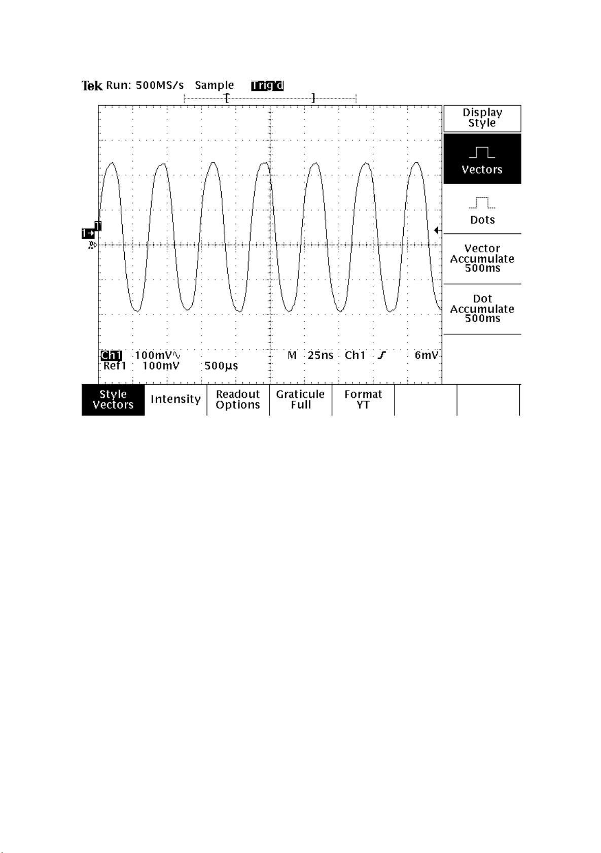
5.2 VIDE O OUTP UT(C HR OMINANC E S IG NAL) C ONFIR MATION
6. MP E G BOAR D C HE C K WAVE FOR M
7.2 MT1389
7.3 HY29LV160 9
7.4 HY57V641620HG
1
1
2
4
5
5
6
7
8
14
8. S C HE MATIC & P C B WIR ING DIAG R AM
15
9. S P AR E P AR TS LIS T 30

1.1 GENERAL GUIDELINES
1. SAFETY PREAUTIONS
2.PREVENTION OF ELECTRO STATIC DISCHARGE(ESD)TO
ELECTROSTATICALLY SENSITIVE(ES)DEVICES
1
1. When servicing, observe the original lead dress. if a short circuit is found, replace all parts which have
been overheated or damaged by the short circuit.
2. After servicing, see to it that all the protective devices such as insulation barrier, insulation papers
shields are properly installed.
3. After servicing, make the following leakage current checks to prevent the customer from being exposed
to shock hazards.
Some semiconductor(solid state)devices can be damaged easily by static electricity. Such components
commonly are called Electrostatically Sensitive(ES)Devices. Examples of typical ES devices are integrated
circuits and some field-effect transistors and semiconductor chip components. The following techniques
should be used to help reduce the incidence of component damage caused by electro static discharge(ESD).
1. Immediately before handling any semiconductor component or semiconductor-equipped assembly, drain
off any ESD on your body by touching a known earth ground. Alternatively, obtain and wear a commercially
availabel discharging ESD wrist strap, which should be removed for potential shock reasons prior to
applying power to the unit under test.
2. After removing an electrical assembly equipped with ES devices,place the assembly on a conductive
surface such as alminum foil, to prevent electrostatic charge buildup or exposure of the assembly.
3. Use only a grounded-tip soldering iron to solder or unsolder ES devices.
4. Use only an anti-static solder removal device. Some solder removal devices not classified as anti-static
(ESD protected)can generate electrical charge sufficient to damage ES devices.
5. Do not use freon-propelled chemicals. These can generate electrical charges sufficient to damage ES
devices.
6. Do not remove a replacement ES device from its protective package until immediately before you are
ready to install it. (Most replacement ES devices are packaged with leads electrically shorted together by
conductive foam, alminum foil or comparable conductive material).
7. Immediately before removing the protective material from the leads of a replacement ES device, touch
the protective material to the chassis or circuit assembly into which the device will be installed.
Caution
Be sure no power is applied to the chassis or circuit, and observe all other safety precautions.
8. Minimize bodily motions when handling unpackaged replacement ES devices. (Otherwise harmless motion
such as the brushing together of your clothes fabric or the lifting of your foot from a carpeted floor can
generate static electricity(ESD).
notice (1885x323x2 tiff)
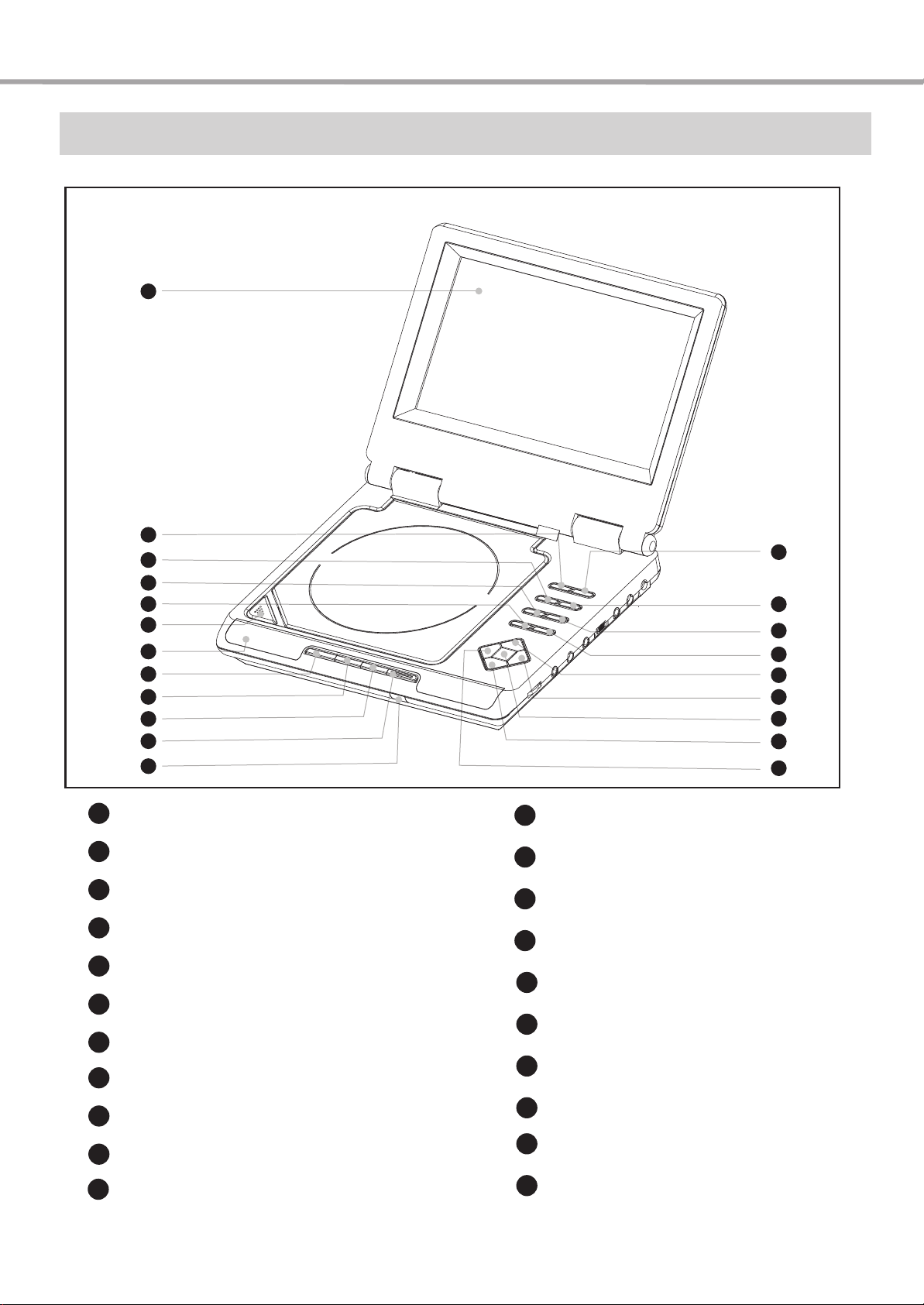
Control Button Locations and Explanations
2
1
2
3
4
5
6
7
8
9
10
11
12
21
20
19
18
17
16
15
14
13
1
Color TFT LCD
2
REW Button
3
P/N button
4
Keyboard Button
5
SETUP Button
6
OPEN/CLOSE button
7
Speakers
8
PLAY button / PAUSE button
9
PREV Button
10
NEXT Button
11
Power indicator
12
IR sensor
13
LEFT direction arrow
DOWN direction arrow
14
15
SELECT button
RIGHT direction arrow
16
17
UP direction arrow
MENU Button
18
19
PICTURE button
20
STOP button
21
Forward Button
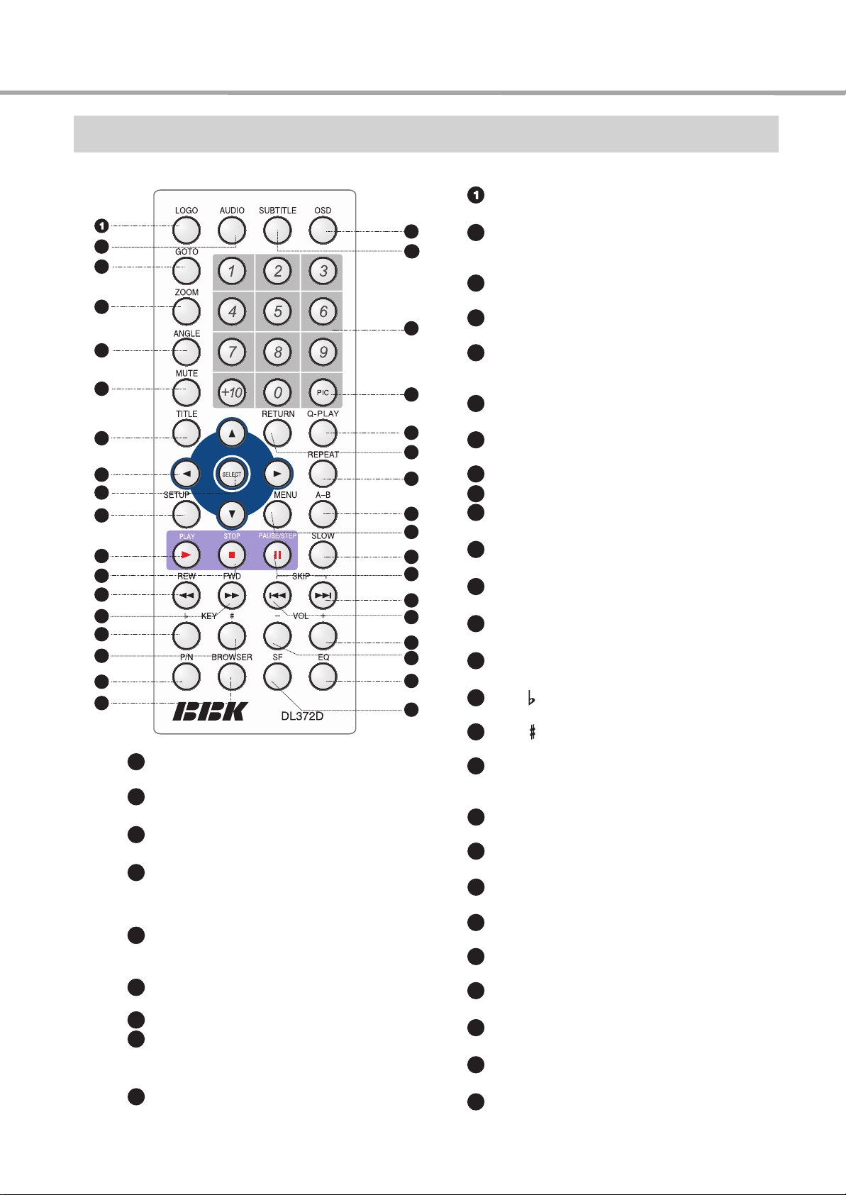
Remote Control Illustration
3
35
10
11
12
13
14
15
16
17
18
2
3
4
5
6
7
8
9
27
MENU Button
Display DVD menu or open/close PBC.
28
A-B Button
Repeat the select.
29
REPEAT Button
Repeat play.
30
RETURN Button
Back to the previous menu/Clearing input
numbers.
31
27
Q-PLAY Button
Skip the advertisement/warning and play
DVD directly.
32
27
PIC Button
Set video.
33
27
NUMBER Buttons
34
SUBTITLE Button
Change subtitle languages/
Switch JPEG display modes.
35
OSD Button
Display or hide disc information.
34
33
32
31
30
29
28
27
26
25
24
23
22
21
20
19
LOGO Button
Set the played image as the power-on logo.
2
AUDIO Button
Change the audio language or
audio channel.
3
GOTO button
Play from the desired location.
4
ZOOM Button
Zoom in /out the displayed frame.
5
ANGLE Button
Change camera angles, MP3/JPEG
playback modes switch.
6
MUTE button
Press once to mute, twice to unmute.
7
TITLE button
DVD titles.
8
CURSOR Buttons
9
SELECT Button
10
SETUP Button
Function setup.
11
PLAY Button
Normal playback.
12
STOP Button
Stop playback.
13
REW Button
Fast backward play.
14
FWD Button
Fast forward play.
15
KEY Button
Fall tone.
16
KEY Button
Rise tone.
17
P/N Button
Switch the TV system between
PAL, NTSC and AUTO.
18
BROWSER
Switch new user interface.
19
SF Button
Adjusting sound field effects.
EQ Button
20
Adjusting equalization effects.
21
VOLUME-
Decrease volume.
22
VOLUME+
Increase volume.
23
PREV Button
Skip backward.
24
NEXT Button
Skip forward.
25
PAUSE/STEP Button
Pause or play frame by frame.
26
SLOW Button
Slow play.
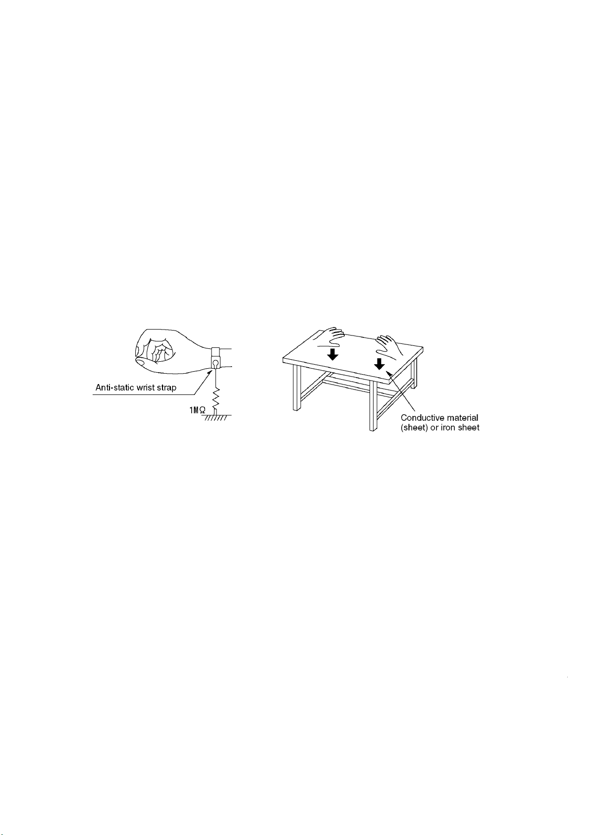
The laser diode in the traverse unit (optical pickup)may brake down due to static electricity of clothes or human
body. Use due caution to electrostatic breakdown when servicing and handling the laser diode.
Some devices such as the DVD player use the optical pickup(laser diode)and the optical pickup will be damaged
by static electricity in the working environment.Proceed servicing works under the working environment where
1. Put a conductive material(sheet)or iron sheet on the area where the optical pickup is placed,and ground the
3. The flexible cable may be cut off if an excessive force is applied to it.Use caution when handling the cable.
4
4.PREVENTION OF STATIC ELECTRICITY DISCHARGE
4.1.Grounding for electrostatic breakdown prevention
grounding works is completed.
4.1.1. Worktable grounding
sheet.
4.1.2.Human body grounding
1 Use the anti-static wrist strap to discharge the static electricity from your body.
safety_3 (1577x409x2 tiff)
4.1.3.Handling of optical pickup
1. To keep the good quality of the optical pickup maintenance parts during transportation and before
installation, the both ends of the laser diode are short-circuited.After replacing the parts with new ones,
remove the short circuit according to the correct procedure. (See this Technical Guide).
2. Do not use a tester to check the laser diode for the optical pickup .Failure to do so willdamage the laser
diode due to the power supply in the tester.
4.2. Handling precautions for Traverse Unit (Optical Pickup)
1. Do not give a considerable shock to the traverse unit(optical pickup)as it has an extremely high-precise
structure.
2. When replacing the optical pickup, install the flexible cable and cut is short land with a nipper. See the
optical pickup replacement procedure in this Technical Guide. Before replacing the traverse unit, remove
the short pin for preventingstatic electricity and install a new unit.Connect the connector as short times as
possible.
4. The half-fixed resistor for laser power adjustment cannot be adjusted. Do not turn the resistor.
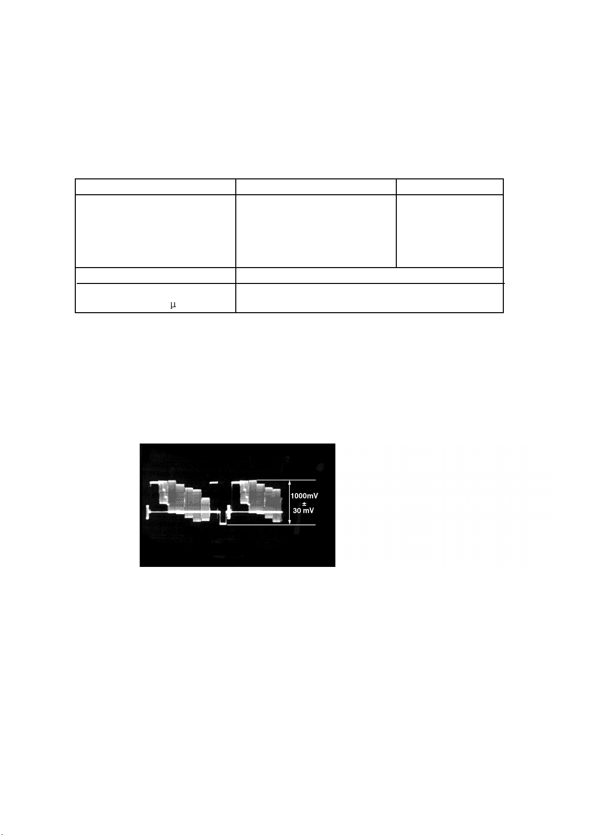
5.1. Video Output (Luminance Signal) Confirmation
5
5.Electrical Confirmation
DO this confirmation after replacing a P.C.B.
Measurement point
Video output terminal
Measuring equipment,tools
200mV/dir,10 sec/dir
Purpose:To maintain video signal output compatibility.
1.Connect the oscilloscope to the video output terminal and terminate at 75 ohms.
2.Confirm that luminance signal(Y+S)level is 1000mVp-p±30mV
PLAY(Title 46):DVDT-S15
PLAY(Title 12):DVDT-S01
Mode Disc
Color bar 75%
Confirmation value
1000mVp-p±30mV
DVDT-S15
or
DVDT-S01
Do the confirmation after replacing P.C.B.
Screwdriver,Oscilloscope
5.2 Video Output(Chrominance Signal) Confirmation
6
Measurement point
Video output terminal
Measuring equipment,tools Confirmation value
200mV/dir,10 sec/dir
Purpose:To maintain video signal output compatibility.
1.Connect the oscilloscope to the video output terminal and terminate at 75 ohme.
2.Confirm that the chrominance signal(C)level is 621 mVp-p±30mV
PLAY(Title 46):DVDT-S15
PLAY(Title 12):DVDT-S01
Mode Disc
Color bar 75%
621mVp-p±30mV
DVDT-S15
or
DVDT-S01
6.MPEG BOARD CHECK WAVEFORM
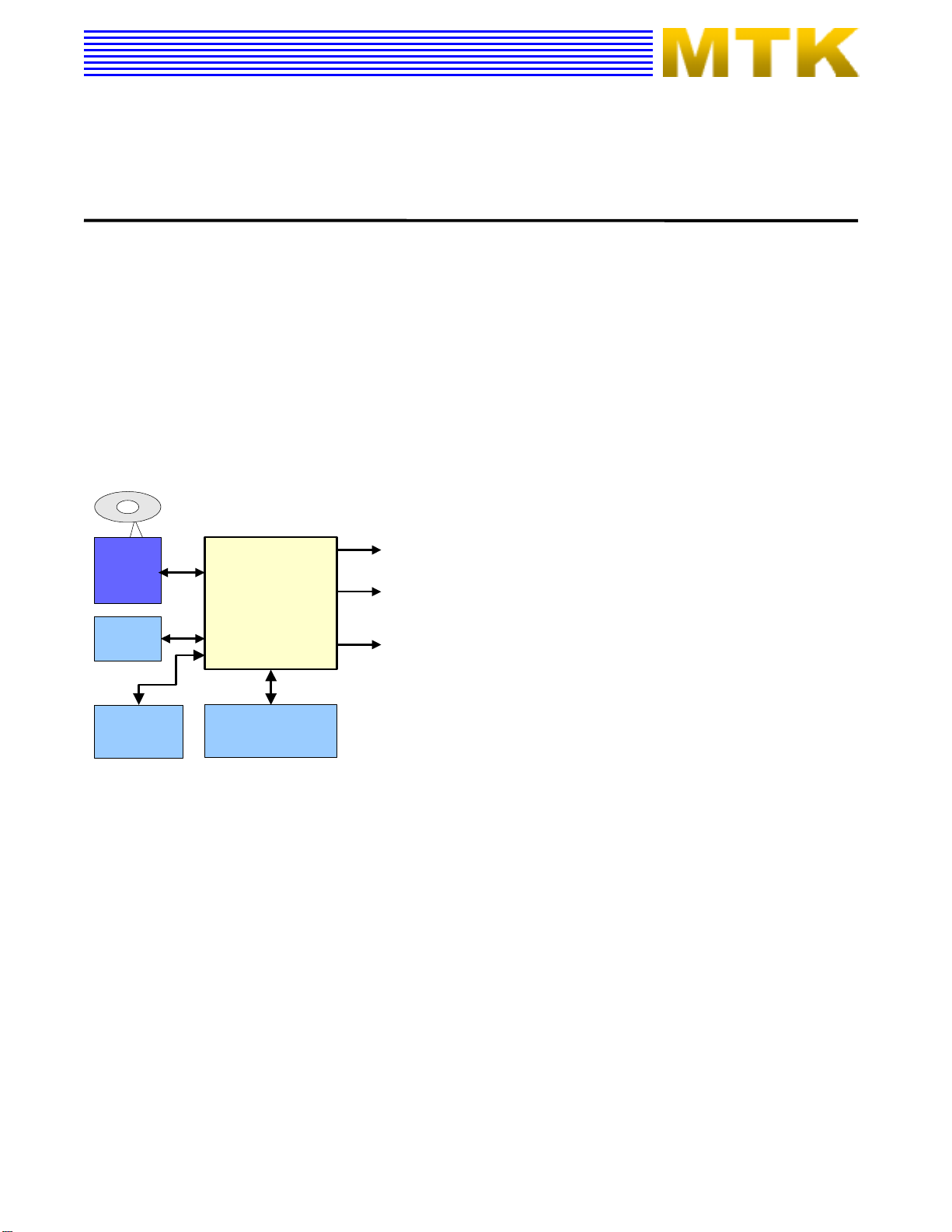
6.1 27MHz WAVEFORM
7
7.2 MT1389
8
MT1389
Specifications are subject to change without notice
Progressive-Scan DVD Player SOC
MediaTek MT1389 is a DVD player system-on-chip (SOC) which incorporates advanced features like high
quality TV encoder and state-of-art de-interlace processing. The MT1389 enables consumer electronics
manufacturers to build high quality, cost-effective DVD players, portable DVD players or any other home
entertainment audio/video devices.
rd
Based on MediaTek’s world-leading DVD player SOC architecture, the MT1389 is the 3
player SOC. It integrates the MediaTek 2
decoder.
The progressive scan of the MT1389 utilized a proprietary advanced motion-adaptive de-interlace algorithm to
achieve the best movie/video playback. It can easily detect 3:2/2:2 pull down source and restore the correct
original pictures. It also supports a patent-pending edge-preserving algorithm to remove the saw-tooth effect.
nd
generation front-end analog RF amplifier and the Servo/MPEG AV
generation of the DVD
Key Features
RF/Servo/MPEG Integration
High Performance Audio Processor
Motion-Adaptive, Edge-Preserving De-interlace
108MHz/12-bit, 6 CH TV Encoder
Applications
Standard DVD Players
Portable DVD Players
DVD
PUH
Module
FLASH
Front-panel
Remote
CVBS, Y/C,
Component
SDPIF
MT1389E
Audio L
Audio R
SDRAM
DVD Player System Diagram Using MT1389

KEY FEATURES
IC BLOCK DIAGRAM & DESCRIPTION
9
HY29LV160
16 Mbit (2M x 8/1M x 16) Low Voltage Flash Memory
nn
n Single Power Supply Operation
nn
– Read, program and erase operations from
2.7 to 3.6 volts
– Ideal for battery-powered applications
nn
n High Performance
nn
– 70, 80, 90 and 120 ns access time
versions
nn
n Ultra-low Power Consumption (Typical
nn
Values At 5 Mhz)
– Automatic sleep mode current: 1 µA
– Standby mode current: 1 µA
– Read current: 9 mA
– Program/erase current: 20 mA
nn
n Flexible Sector Architecture:
nn
– One 16 KB, two 8 KB, one 32 KB and
thirty-one 64 KB sectors in byte mode
– One 8 KW, two 4 KW, one 16 KW and
thirty-one 32 KW sectors in word mode
– Top or bottom boot block configurations
available
nn
n Sector Protection
nn
– Allows locking of a sector or sectors to
prevent program or erase operations
within that sector
– Sectors lockable in-system or via
programming equipment
– Temporary Sector Unprotect allows
changes in locked sectors (requires high
voltage on RESET# pin)
nn
n Fast Program and Erase Times
nn
– Sector erase time: 0.25 sec typical for
each sector
– Chip erase time: 8 sec typical
– Byte program time: 9 µs typical
nn
n Unlock Bypass Program Command
nn
– Reduces programming time when issuing
multiple program command sequences
nn
n Automatic Erase Algorithm Preprograms
nn
and Erases Any Combination of Sectors
or the Entire Chip
nn
n Erase Suspend/Erase Resume
nn
– Suspends an erase operation to allow
reading data from, or programming data
to, a sector that is not being erased
– Erase Resume can then be invoked to
complete suspended erasure
nn
n Automatic Program Algorithm Writes and
nn
Verifies Data at Specified Addresses
nn
n 100,000 Write Cycles per Sector Minimum
nn
nn
n Data# Polling and Toggle Bits
nn
– Provide software confirmation of
completion of program and erase
operations
nn
n Ready/Busy# Pin
nn
– Provides hardware confirmation of
completion of program and erase
operations
nn
n Hardware Reset Pin (RESET#) Resets the
nn
Device to Reading Array Data
nn
n Compliant With Common Flash Memory
nn
Interface (CFI) Specification
– Flash device parameters stored directly
on the device
– Allows software driver to identify and use
a variety of different current and future
Flash products
nn
n Compatible With JEDEC standards
nn
– Pinout and software compatible with
single-power supply Flash devices
– Superior inadvertent write protection
nn
n Space Efficient Packaging
nn
– 48-pin TSOP and 48-ball FBGA packages
LOGIC DIAGRAM
20
A[19:0]
CE#
OE#
WE#
RESET#
BYTE#
DQ[7:0]
DQ[14:8]
DQ15/A-1
RY/BY#
8
7
Preliminary
Revision 1.0, June 2000
 Loading...