

Page 1

DL370D
servicemanual
Page 2

Catalog
ChapterOneAboutMaintenance 1
1.1Safetyprecautions
1.1.1Powersupply
1.1.2Precautionsforantistatic
1.1.3Precautionsforlaserhead
1.1.4Aboutplacementposition
1.2Maintenancemethod
1.2.1Visualizedmethod
1.2.2Electricresistancemethod
1.2.3Voltagemethod
1.2.4Currentmethod
1.2.5Cuttingmethod
1.2.6Elementsubstitutionmethod
1.2.7Comparisonmethod
1.3Requireddeviceformaintenance
1
1
1
1
2
2
2
2
2
2
2
3
3
3
ChapterTwoFunctionsandOperationInstructions
2.1Features
2.2ControlButtonLocationsandExplanations
2.3RemoteControlIllustration
2.4Accessories
2.5FUNCTIONSETUP
2.5.1FunctionSetup
2.5.2GeneralSettings
2.5.3AudioSetup
2.5.4InitialSetup
2.5.5Usefulnotes
2.6Specifications
4
4
4
6
7
7
7
7
8
8
9
9
Page 3

ChapterThreePrincipleorServicing
10
SectionOnePrincipleofthePlayer
3.1.1Blockdiagramoftheplayer
3.1.2PCBcompositionblockdiagramoftheplayer
3.1.3FunctionintroductiontoICoftheplayer
SectionTwoUnitCircuitPrinciple
3.2.1Servoprocessingcircuit
3.2.2CD/DVDswitchcircuit
3.2.3Laserpowercontrolcircuit
3.2.4Mainaxiscontrolcircuit
3.2.5DC-DCswitchcircuit
3.2.6Batteryvoltagedetectingcircuit
3.2.7Audiooutputcircuit
3.2.8Screenoffdetectcontrolcircuit
3.2.9VideocodingandLCDTFTdrivecircuit
3.2.10Chargecircuitandprotectioncircuit
10
10
11
11
13
13
15
16
17
17
19
20
21
22
25
3.2.11Controlpanelcircuitandremotecontrolcircuit
3.2.12Decodecircuit
3.2.13Resetcircuit
3.2.14Mutecircuit
SectionServicingCases
3.3.1Servicinginstances
3.3.2Troubleshootingflowchart
SectionFourServicingParameters
3.4.1Signalwaveformdiagram
SectionFiveFunctionIntroductiontoIC
3.5.1functionintroductiontoMT1389E
3.5.2functionintroductiontoAM5898N
3.5.3functionintroductiontoHWD4863
3.5.4functionintroductiontoS3C9454
3.5.5functionintroductiontoT102
26
26
28
29
30
30
34
44
44
51
51
62
62
63
65
ChapterFourDisassemblyandAssemblyProcess
70
Page 4

ChapterCinquePCBboard&Circuitdiagram
76
SectionOnePCBboard
SectionTwocircuitdiagram
ChaptersixBOMList
upgradeboardunit
6.1
batteryboard
6.2
batterycase
6.3
batterychargeboard
6.4
6.5
batteryconnectingboard
batteryprotectboard
6.6
6.7
decodeboard
driveboard
6.8
mainpanel
6.9
powersocketboard
6.10
76
85
94
94
94
94
95
96
96
97
101
102
103
Page 5

Chapter One About Maintenance
1.1 Safety precautions
1.1.1 Power supply
When maintenance personnel are repairing DVD players, he should pay special attention to the
power board with 220V AC and 330V DC which will cause hurt and damage to persons!
1.1.2 Precautions for antistatic
Movement and friction will both bring static electricity which causes serious damages to integrated
IC. Though static charge is little, when a limited quantity of electric charge is added to large-
scaleintegrated IC, as the capacitance is very small in the meantime, now the integrated IC is very much
easy to be struck through by static electricity or the performance will decrease. Thus static electricity
prevention is of extraordinary importance. The following are several measures to prevent static
electricity:
1. Use a piece of electric conduction metal with the length of about 2 metres to insert into the earth,
and Fetch the lead wire from the top of the surplus metal and connect to the required static electricity
device. The length and depth of the metal embedded under the earth should be determined according to
the wettability of the local soil. For humid places, it may be shorter, and longer and deeper for dry places.
If possible, it can be distributed and layed in terms of “#” shape.
2. On operating table-board, the antistatic table cushion should be covered and grounded.
3. All devices and equipments should be placed on the antistatic table cushion and grounded.
4. Maintenance personnel should wear antistatic wrist ring which should be grounded.
5. Places around the operating position should also be covered with electric conduction cushion or
Painted with antistatic paint.
1.1.3 Precautions for laser head
1. Do not stare at laser head directly, for laser emission will occur when laser head is working, which
will Hurt your eyes!
2. Do not use wiping water or alcohol to clean laser head, and you may use cotton swab.
- 1 -
Page 6

1.1.4 About placement position
1. Never place DVD player in positions with high temperature and humidity.
2. Avoid placing near high magnetic fields, such as loudspeaker or magnet.
3. Positions for placement should be stable and secure.
1.2 Maintenance method
1.2.1 Visualized method
Directly view whether abnormalities of collision, lack of element, joint welding, shedding welding,
rosin joint, copper foil turning up, lead wire disconnection and elements burning up among pins of
elements appear. Check power supply of the machine and then use hands to touch the casing of part of
elements and check whether they are hot to judge the trouble spot. You should pay more attention when
using this method to check in high voltage parts.
1.2.2 Electric resistance method
Set the multimeter in resistance position and test whether the numerical value of resistance of each
point in the circuit has difference from the normal value to judge the trouble spot. But in the circuit the
tested numerical value of resistance is not accurate, and the tested numerical value of integrated IC's
pins can only be used for reference, so the elements should be broken down for test.
1.2.3 Voltage method
Voltage method is relatively convenient, quick and accurate. Set the multimeter in voltage position
and test power supply voltage of the player and voltage of a certain point to judge the trouble spot
according to the tested voltage variation.
1.2.4 Current method
Set the multimeter in current position and test current of the player of a certain point to judge the
trouble spot. But when testing in current method, the multimeter should be series connected in the
circuit, which makes this method too trivial and troublesome, so it is less frequently used in reality.
1.2.5 Cutting method
Cutting method should be combined with electric resistance method and voltage method to use.
This method is mainly used in phenomena of short circuit and current leakage of the circuit. When
cutting the input terminal voltage of a certain level, if voltage of the player rises again, it means that the
trouble lies in this level.
- 2 -
Page 7

1.2.6 Element substitution method
When some elements cannot be judged good or bad, substitution method may de adopted directly.
1.2.7 Comparison method
A same good PC board is usually used to test the correct voltage and waveform. Compared these
data with those tested through fault PC board, the cause of troubles may be found.
Through the above maintenance method, theoretical knowledge and maintenance experience, all
difficulties and troubles will be readily solved.
1.3 Required device for maintenance
Digital oscillograph ( 100MHE)
TV set
SMD rework station
Multimeter
Soldering iron
Pointed-month pincers
Cutting nippers
Forceps
Electric screw driver
Terminals connecting cord
Headphone
Microphone
- 3 -
Page 8

ChapterTwo
FunctionsandOperationInstructions
2.1Features
ThisplayerutilizescolorTFTLCDandnewgenerationDVDdecodingchipwithbuilt-inDolbyDigital
decoderswhichcanbringyoutoabrand-newAVentertainmentworld.The2-lasersupererrorcorrection
mechanismsupportsCD-R
Brand-newAVEffects.
1.7”colorTFTLCD.
CompatiblewithMPEG4discstoproducewonderfulpictures.
2.
3.Built-inDolbyDigitaldecoder.
4.Built-instereospeakers.
5.Hi-Fistereoheadphoneoutput.
HighQualityDigitalAudio
1.Built-inDolbyDigitalandDTSdigitalsurrounddecoder
NumerousConvenientFunctions
1.ScreensaverfunctioncautiouslyprotectsyourLCDandTV.
2.LargecapacitysolidLi-Ionbattery,electronicanti-shockcircuits,convenientforyoutowatchmovies
outdoors.
3.Easy-to-usebrand-newGUIandvirtualkeyboard.
4.Multi-angleplaybackfunctionmakesitpossibleforyoutoviewascenefromdifferentcameraangles.
5.Directentrytodesiredscenes(title/chapter/time/tracksearch).
6.MultipleaspectratiostofitvariousTVsets.
7.Parentalcontrolfunctiontoprotectchildrenfromwatchinginappropriatediscs.
8.Multipledubbinglanguagesandsubtitlelanguageskeepyouinthebestentertainingstatusanytime.
SupportsSVCD,VCD,CD,MP3,HDCD,KODAKPICTURECD,DVD-R/RW.
:SomediscslabelledwithMPEG4onthemarketactuallyare*.rm/*.ram/*.rmm/*.raandothers
NOTE
whichareimcompatible.Pleasetakecarewhenbuyingdiscs.
2.2ControlButtonLocationsandExplanations
1
2
3
4
5
6
7
8
9
10
11
-4-
19
18
17
16
15
14
13
12
Page 9
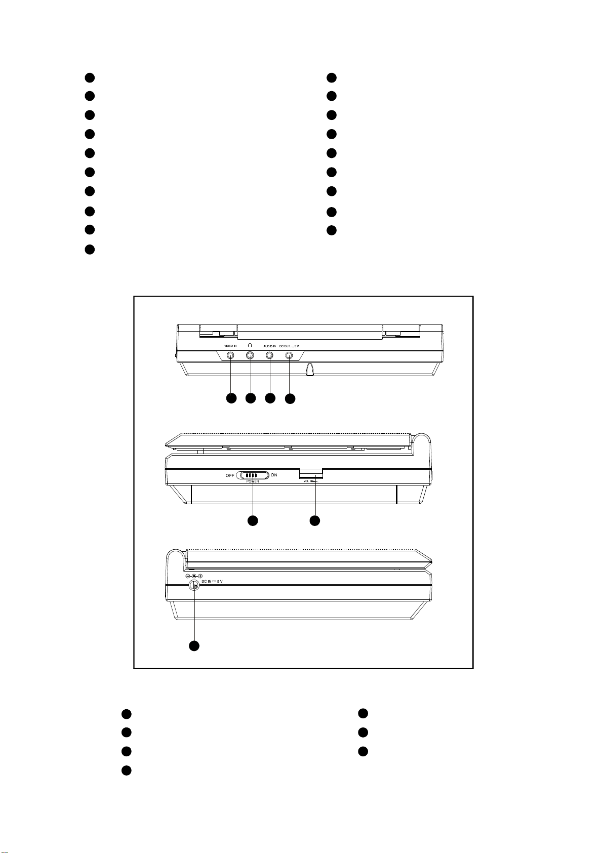
1
ColorTFTLCD
11
Powerindicator
2
Speakers
3
PICTUREButton
4
DVD/AUXINButton
5
SETUPButton
6
FWDButton/UPdirectionarrow
7
PREV/LEFTButton
8
OPEN/CLOSEButton
9
PLAY/SELECTbutton
10
PAUSEbutton
12
IRsensor
13
STOPButton
14
Keyboard/SWITCHButton
15
REWButton/
16
NEXT/RIGHTButton
17
MENUButton
18
TITLEButton
19
Q-PLAYButton
DOWNdirectionarrow
1 2 3
5 6
7
4
1
VideoInjack
2
HeadPhonesjack
3
AudioInjack
4
DC5VOut
-5-
5
Powerswitch
6
Speakervolumeknob
7
DC9VIn
Page 10
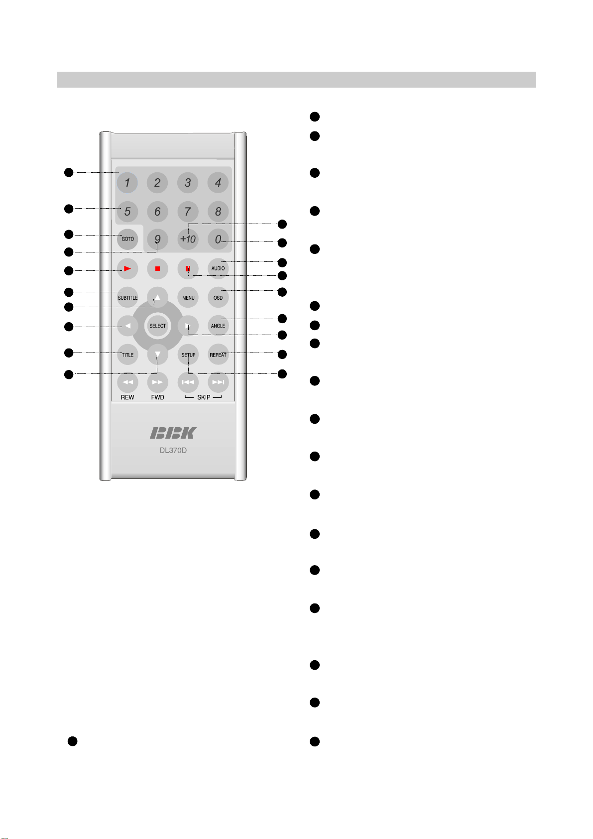
2.3RemoteControlIllustration
1
2
3
4
5
6
7
8
9
10
1
NUMBERButtons
2
GOTObutton
Playfromthedesiredlocation.
3
PLAYButton
Normalplayback.
4
STOPButton
19
18
17
16
15
14
13
12
Stopplayback.
5
SUBTITLEButton
Changesubtitlelanguages/SwitchJPEG
displaymodes.
6
CURSORButtons
7
SELECTButton
8
TITLEbutton
DVDtitles.
11
9
REWButton
Fastbackwardplay.
10
FWDButton
Fastforwardplay.
11
PREVButton
Skipbackward.
12
NEXTButton
Skipforward.
13
SETUPButton
Functionsetup.
14
REPEATButton
Repeatplay.
15
ANGLEButton
Changecameraangles,MP3/JPEGplayback
modesswitch.
16
MENUButton
DisplayDVDmenuoropen/closePBC.
17
OSDButton
19
PAUSEButton
Pauseframebyframe.
-6-
Displayorhidediscinformation.
18
AUDIOButton
Changetheaudiolanguageoraudiochannel.
Page 11

2.4Accessories
AVCords
RemoteControl
AAASizeBatteries
InstructionManual
BatteryPack
PowerAdapter
WarrantyCard
2.5FUNCTIONSETUP
2.5.1FunctionSetup
1.PressSETUPbutton,TheTVsetscreen
displays:
1PCS
1PCS
2PCS
1PCS
1PCS
1PCS
1PCS
4.PressUP/DOWNarrowtoselectthedesired
value.PressSELECTtoconfirmit.
Forexample:PressUP/DOWNarrowtoselect
"LT/RT",thanpressSELECT,theTVscreen
Display:
————AudioSetupPage
AudioMode
EQType
SoundField
Tone
DolbyDigitalSetup
LT/RT
Stereo
VSURR
00
5.PressSETUPtoexitthesetupmenu.
————GeneralSetupPage
TVDisplayWide
OSDLangEnglish
ScreenSaverOn
Spectrum
Off
2.PressLEFT/RIGHTarrowtoselectthe
desiredchanneltobechanged.
Forexample,ifyouwanttosetthisplayer's
Audio,pleasepressLEFT/RIGHTarrowsto
selectAUDIOSETUPPAGE.PressSELECTfor
verification.Theaudiosetuppagedisplays
Onthescreen.
————AudioSetupPage
AudioMode
EQType
SoundField
Tone
DolbyDigitalSetup
LT/RT
Stereo
VSURR
3.PressUP/DOWNarrowtoselectthedesired
itemyouwanttosetandpressSELECT.
Forexample,pressUP/DOWNarrowsto
selectAUDIOMODEandpressSELECT.The
AUDIOMODEappearsonthescreen.
————AudioSetupPage
AudioMode
EQType
SoundField
Tone
DolbyDigitalSetup
LT/RT
Stereo
VSURR
CURSOR
SETUP
SELECT
2.5.2GeneralSettings
————GeneralSetupPage
TVDisplayWide
OSDLangEnglish
ScreenSaverOn
Spectrum
1.TVDisplay
:Tosettheaspectratioofthis
player'soutputimage.
Optionalsettings:NORMAL/PANSCAN,
◆
NORAM/LETTERBOX,WIDE.
Default:WIDE.
◆
NOTES
Theplayingeffectsarecontingentuponthe
◆
disc'srecordingaspectratio.Somediscsmay
notbeplayedaccordingtoyourselected
aspectratio.
16:9isonlyapplicabletothe16:9TV.
◆
Pleaseselecttheaspectrationinaccordance
◆
withthatofyourTV.
TheLCDscreenisutilizing16by9aspect
◆
ratioonly.
2.
OSDLang:Thisitemisusedtosetthe
promptslanguageonthescreen.
Optionalsettings:English,Russian.
◆
Default:English.
◆
3.
Screensaver:Openorclose thescreensaver
Function.
Optionalsettings:OFF,ON
◆
Off
-7-
Page 12

◆Default:ON
4.Spectrum:Thisitemisusedtosetwhetherthe
DynamicSpetrumisallowed.
Selectablevalue:ON,OFF.
◆
Default:OFF
◆
2.5.3AudioSetup
————AudioSetupPage
AudioMode
EQType
SoundField
Tone
DolbyDigitalSetup
1.
Audiooutputmode:Tosettheaudiooutput
modetomakethemulti-channelaudiointo
two-channeloutputs.
Optionalsettings:LT/RT,STEREO,VSURR.
◆
Default:STEREO
◆
2.
EQtype:TosetEQmodes.
Optionalsettings:Off,ROCK,Pop,Live,Dance,
◆
Techno,Classic,Soft.
Default:Off
◆
3.SoundField
Optionalsettings:Off,Concert,Livingroom,
◆
:Tosetdifferentsoundfieldeffects.
Hall,Bathroom,Cave,Arena,Church.
Default:Off.
◆
4.TONEcontrol:Thisitemisusedtosetthetone
leveltomatchyourdiapasonwhenyouare
singing.
Methodtoadjusttone:
◆
A.PressUP/DOWNcursorbuttontoselect
TONEiteminAUDIOSETUPPAGE,andthen
pressSELECTbuttontoentertheadjustmenu
B.PressLEFT/RIGHTcursorbuttontoadjustthe
settingvalue.
C.PressSELECTbuttonto returntoAUDIO
SETUPPAGEafteradjustmentarewelldone.
5.
DolbyDigitalsetup:
A.
L+R:Tosettheoutputmeansoftheleftor
rightaudiowhenplayingaDolbydiscwith
separatetwo-channelaudio
Optionalsettings:Stereo,L-Mono,R-Mono,
◆
Mix-Mono.
Default:Stereo.
◆
B.
Dynamiccompression:Tosetthelinear
compressionratiotogetdifferentcompression
result.
Optionalsettings:OFF1/81/43/81/2
◆、、、、、
5/83/47/8FULL
、、、。
Default:OFF.
◆
Stereo
Off
Off
00
2.5.4InitialSetup
————PreferencePage
PBC
Audio
Subtitle
DiscMenu
Parental
Password
Default
1.PBC:TosetthePBCstatus.
◆
WhenplayingSVCDorVCD2.0discs,ifthe
PBCisON,themenuimagedisplaysonthe
screenandthisplayerenterthePBCmode;if
thePBCisOFF,thisplayerplaysthediscby
itssequence.
◆
Optionalsettings:On,Off.
◆
Default:On.
2.AUDIO
:Tosetthepreferenceaudiolanguage
whenplaying.
3.
SUBTITLE:Tosetthepreferencesubtitle
languagewhenplaying.
◆
Optionalsubtitlelanguages:English,French,
Spanish,Chinese,Japanese,korean,Russian,
Thai,others,Off.
◆
subtitlelanguagedefault:Off
4.
DISCMENULANGUAGE:Tosetthe
preferencediscmenulanguagewhenplaying.
◆
Optionalaudio/discmenulanguages:English,
French,Spanish,Chinese,Japanese,korean,
Russian,Thai,others.
◆
Audio/discmenulanguagedefault:English.
NOTES
◆
Audio/subtitle/discmenulanguagesare
effectivetoDVDonly.
◆
Ifthediscdoesnotrecordyourdesired
language,theplayerwillselectthediscspecifiedlanguagestoplay.
◆
Selectingotherlanguages:PressUP/DOWN
ARROWtomovethecursortoOTHERitem,
pressSELECT.PressNUMBERbuttonsto
enteryourdesiredlanguagecodes,thenpress
SELECT.
5.
Parental:Tosettheparentalcontrolratingsto
preventchildrenfromwatchingtherestricted
contents.(Incasethediscsupportsthis
function.)
◆
Optionalsettings:KID,G,PG,PG-13,PGR,R,
NC17,ADULT,OFF.
◆
Default:OFF.
NOTE
On
English
Off
English
Off
-8-
Page 13

◆◆Whenchangingtheparentalcontrolratings,apasswordisneeded.Refertothefollowingpassword
itemfordetailedsettings.
PASSWORD:Tosetafourdigitpasswordtoenableyoutochangetheparentalcontrolratings.
6.
Default:7890.
OLDPASSWORD
NEWPASSWORD
CONFIRMPWD
OK
7.
DEFAULT:Torestoreallsettingstothedefaultvalueexceptfortheparentalcontrolandpassword
settings.
2.5.5Usefulnotes
Inordertoprolongtheservicelifeofyourplayer,itisrecommendedtowaitatleast30secondsbefore
◆
youturnitonagainafterswitchingitoff.
Turnoffpowerafteroperation.
◆
Onlyusethepowersupplyofthenominalvoltage,otherwisetheplayerwillnotbeoperationaloreven
◆
bedamaged.
Somefunctionsoftheplayermaynotbeapplicabletosomediscs.
◆
Incaseofoccasionalplayerhalt,pleaseturnitoffandturnitonagain.
◆
ThisplayercannotplaysomeSVCDdiscswiththeCVDformat.
◆
WhentousetheAudioOutputofthisunit,pleaseminimizethephonevolumefirst.
◆
2.6Specifications
DVD VIDEO
SVCD,MPEG4
Disc Types
Output
Video
Characteristics
Audio
Characteristics
General
Specifications
Operating
Temperature
Operating
Humidity
VCD1.0,1.1,2.0
CD-DA
MP3
Analog audio output Stereo output,
Video Output
Video Amplitude 1.0Vp-p(75Ω)
Frequency 20Hz~20kHz(±1dB)
Signal-to-noise Ratio >90dB
Total harmonic distortion <0.01%
Power Supply DC 9V 2A
Power Consumption 12W
Dimensions 205mmX149mmX39.5mm
Mass 735g
5℃~35℃
15%~75%(no condensation)
Headphone output
◆◆Specificationsaresubjecttochangewithoutnotice.
Wedonotgraranteethatalldiscscanbeplayedsmoothlyduetothediscquality,discrecordingquality
andrecordingformat.
-9-
Page 14
ChapterThreePrincipleorServicing
SectionOnePrincipleofthePlayer
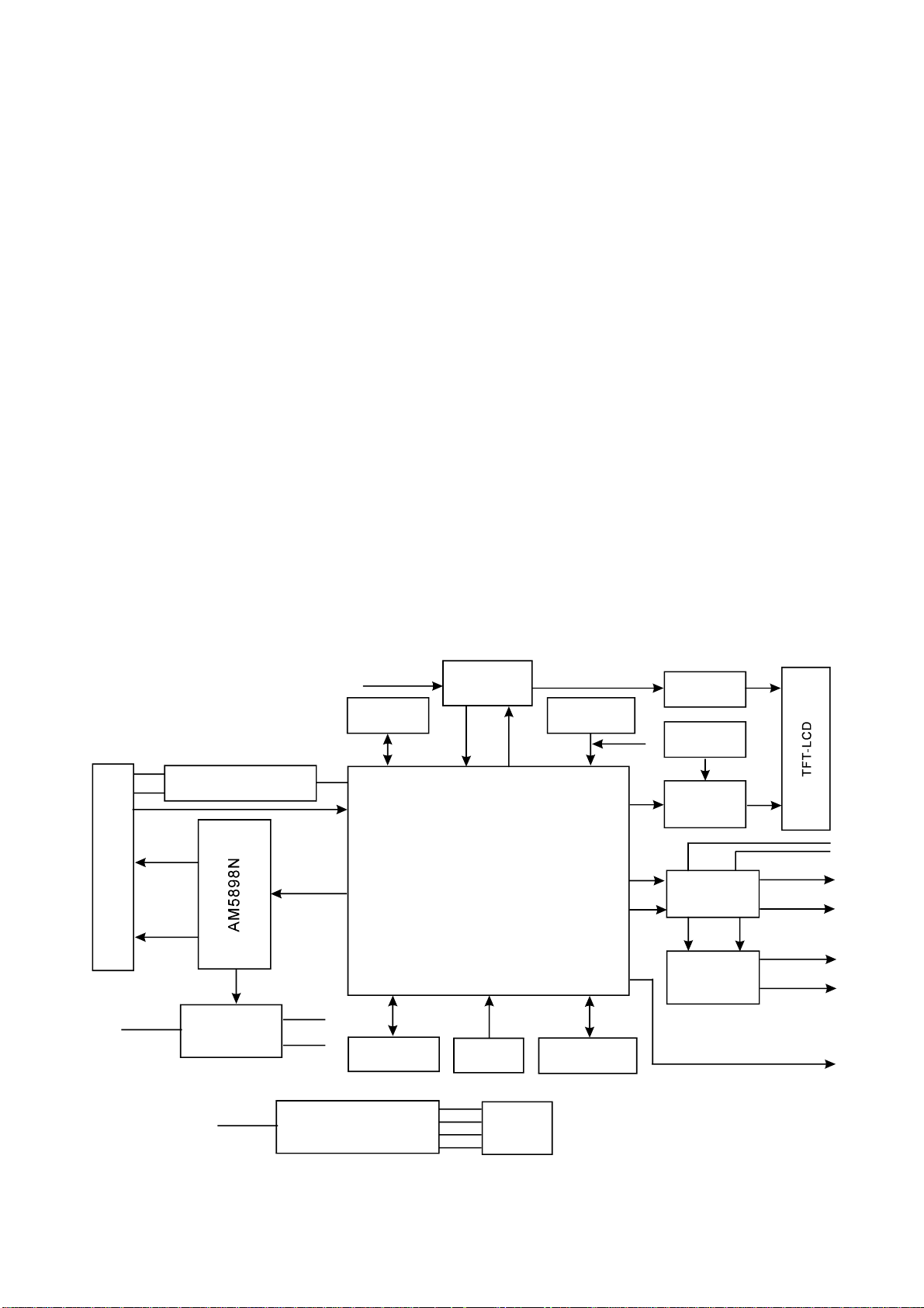
3.1.1Blockdiagramoftheplayer
DL370Discomposedofdecodecircuit,servocircuit,audiocircuit,videocircuitandpowercircuit.
Theblockdiagramoftheplayerisshownasinthefollowingfigure3.1.1.1:
Loader
Feed,
mainaxis
drive
+9VIN
Discswitchand
APCcircuit
Focus,
trace
drive
conversioncircuit
DC-DC
+9VIN
U204
AT24C02
Servodrive
signalinput
VCC
Dv33
FLASH(16M)
Chargecontrolcircuit
Sw601
Screenoff
detectcontrol
circuit
BL_CLT#
STBT
MT1389E
Resetcircuit
components
Battery
BL_CLT
Ht6222
Buttonscontrol
VSAD
SDRAM()64M
Boostboard
IR
AL LOUT
AR
27MHz
LCDdrive
T102
ALIN
Audiofiltering/
amplifying
Headphone/
speaker
amplifying
LM4863
ARIN
ROUT
LSOUT
RSOUT
CVBS1
Figure3.1.1.1Blockdiagramoftheplayer
-10-
Page 15

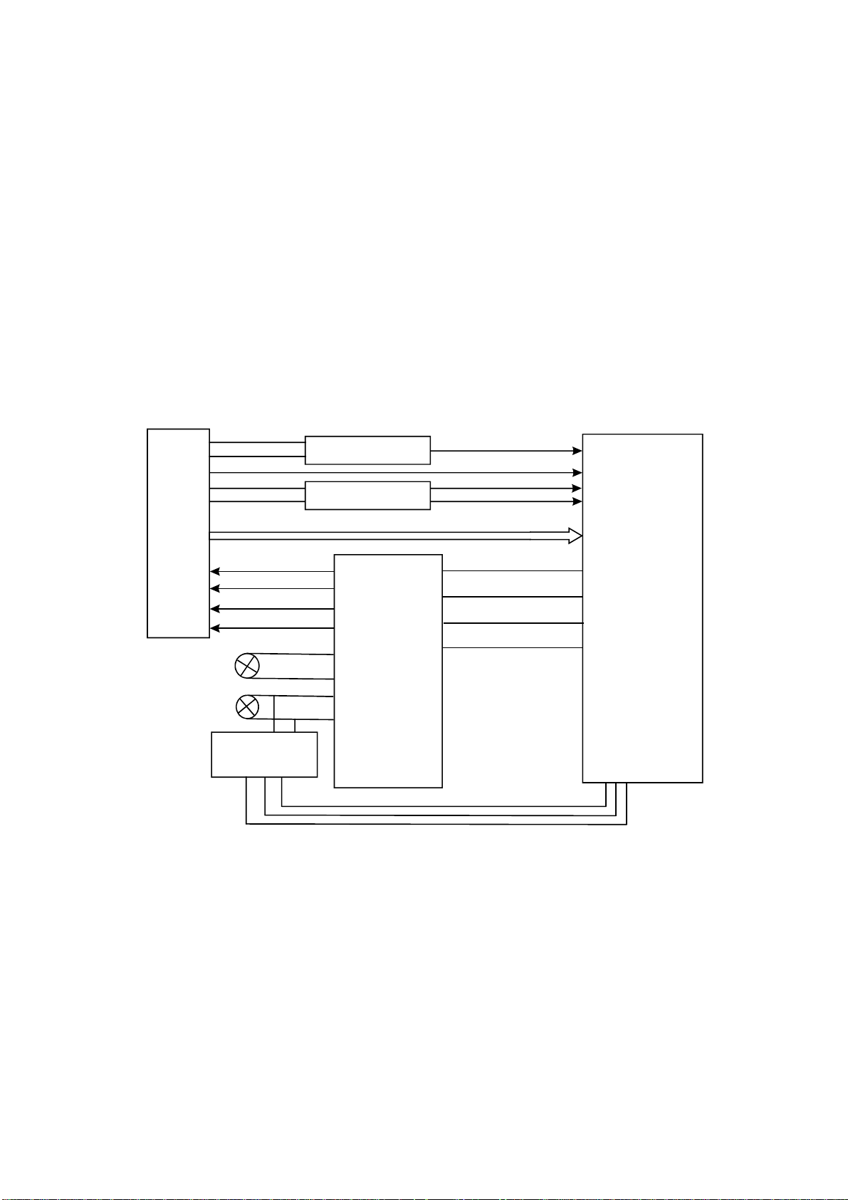
3.1.2PCBcompositionblockdiagramoftheplayer
PCBcompositiondiagramoftheplayerisshownasinthefollowingfigure3.1.2.1:
VOUT+
Battery
components
TEMP
Jk602
Chargeboard
GND
DCsocketboard
Loader
Jk603
VIN+9V
COUT-
9VIN
PGND
BATTY_LED
CHECK
COVER_SW
SPSP+
SL+
SL-
LIMIT
Mainpanel
GND
STV1
STV2
CKV
U/D
OEV
VCOMO
GND
OEH
STH2
STH1
GND
CPH1
GND
VR
VG
VB
GND
VSDA
Xs801
Xs701
BLGND
BLCLT
BL+9V
+5V
+5V
GND
SRSR+
SLSL-
GND
Jk101
Xs101
A/B/C/D/E/F
Xs102
Figure3.1.2.1PCBcompositionfigureoftheplayer
V33
Xs501
BL9V
Loudspeaker
Jp2
Jp1
Driveboard
Jp3
Jp6
BL
CTL
Boostboard
BL
GND
TFT
LCD
GND
5VA
VGL
VGH
STV1
STV2
CKV
U/D
OEV
VCOM
VCOM
L/R
STH2
STH1
CPH1
CPH1
CPH1
5VA
GND
VR
VG
VB
VDD2
GND
3.1.3FunctionintroductiontoICoftheplayer
FunctionintroductiontoICoftheplayerisshownasinthefollowingfigure:
PCB board Location IC model Function
Main panel U401 PT2222A Buttons coding control
Drive board
Protection board QB1 S8232 Battery charge protection
Charge board
Boost board IC1 MP1026 Boost control
Decode board
U1 NJM3414AM VCOM signal amplifying
U2 G5105TBU DC-DC conversion
U601 S3F9454 8-bit single chip, charge control
U602 TL431
Three-end adjustable distributary reference
source
U603 LM358 Operational amplifier
U301 C4558 Audio amplifying (operational amplifier)
U803 AZ1117 Voltage regulating IC
U202 HY57V641620ET 64M SDRAM
U801 T102 Video coding, LCD drive
-11-
Page 16

U204 24C02 EEPROM
U201 MT1389FE/E Decode chip
U901 AM5898 Servo drive, DC-DC control
Decode board
U502 LM393
Battery electrical charge detect (operational
amplifier)
U701 HWD4863 Headphone amplifying
U206,U802 LM1117H Voltage regulating IC (U206 1.8V/U802 2.5V)
U501 HS0038B3V Receiver
U203 29LV160BE 16M FLASH
-12-
Page 17
SectionTwoUnitCircuitPrinciple
3.2.1Servoprocessingcircuit
1.DL370DadoptsSANYO62loaderandMTKdecodesolution(MT1389E+FLASH(16M)+SDRAM
(64M)).Theservocircuitiscomposedoffrontendsignalprocessing,digitalsignalprocessingIC
MT1389EanddrivecircuitAm5898,inwhichMT1389Eisalsothemaincompositionofdecodecircuit.
XS101
Feedelectricmachine
Mainaxiselectricmachine
Mainaxiscontrol
detectcircuit
Switchcircuit
APCcircuit
ABCDEFRFO
TKTK+
FC+
FC-
SL+
SL-
SP-
SP+
D5898
FOSO
FMSO
TRSO
DMSO
IOA
MD11
LDO2
LDO2
MT1389
Figure3.2.2.1Servoprocessingcircuitblockdiagram
2.Workingprinciple:afterpoweronorturningoffdoor(doordetectswitchSW601/SW602on
chargeboardshoutsoff),loaderlaserheadbeginstoreset,focusandmainaxisbegintorotate,laser
headbeginstoidentifydiscinformationtojudgethediscisCDorDVDtofacilitatetomakethe
correspondingacts.Atthesametime,Mt1389alsoadjustslaseroutputpowerthroughlaserpower
controlcircuit.Whenloaderreadsdiscinformation,afterphotoelectricconversion,A,B,C,D,E,F
signalsareformedtogivetoMt1389(DVDhasA,B,C,Dsignalsonly)andTereforesignalandthe
h
inputfrompin2~11,18,19ofMT1389.AfterMT1389internalpre-amplifyingprocessing,nowsignalare
dividedintotwopartsinsideMT1389:
-13-
Page 18

AfterbeingprocessedbydigitalservosignalcircuitinsideMT1389,onepartofsignalform
correspondingservocontrolsignalsandoutputFOO,TRO,DMO,FMOdigitalservocontrolsignalsfrom
pin42,pin41,pin37,pin38ofMt1389respectively,thenchangeintoanalogservocontrolsignalFOSO,
TRSO,DMSO,FMSOthroughintegrationcircuitcomposedbyresistorcapacitor,andsendtodriver
circuitBA5954foramplificationtobringalongfocuscoil,tracecoil,mainaxiselectricmachineandfeed
electricmachineafterdriveamplification.Amongthese,focusandtraceservoareusedtocorrect
objectivepositionaccurately;feedservoisusedtobringalonglaserheadtomakeradiallarge-scale
movewhichbelongstothepreliminaryadjustmenttopick-upposition;andmainaxisservoisusedto
controlmainaxiselectricmachinetomakeitreadsignalsinmeansofconstantlinearvelocityandbring
alongdisctorotate.AfterprocessingofamplificationbyVGAvoltagecontrolamplifierandequalization
frequencycompensationinsideMT1389,anotherpartofsignalsarechangedintodigitalsignalsthrough
internalA/Dconverter.WhenloaderisreadingCD/VCDsignals,thesesignalsareconductedEFM
demodulationinsideMT1389,afterCIRC(Cross-InterleavedReed-SolomonCode)errorcorrectionis
finishedinside,itoutputstorearstateforaudio/videodecoding;whenloaderisreadingDVDsignals,
thesesignalsareconductedESMdemodulationinsideMT1389,andthensenttolatterstagefor
decodingafterfinishingRSPCerrorcorrectioninside.ComparedwithgeneralDVDplayers,this
machinehasnodiscin/outcircuitandmanualopeningmethodisadopted.Whenpin148ofMT1389Eis
highlevel,systemrecognisesthatthedoorhasbeenopened,when itislowlevel,themachine
recognizesthatthedoorhasbeenclosed.
3.Loadersignalsintroductionisshownasfollows:
Pin Name
1 F- Input loader 2.52 2.34 0.46
2 F+ Input loader 2.49 2.49 0.93
3 T+ Input loader 2.53 2.51 0.94
4 T- Input loader 2.58 2.51 0.93
5 C Input MT1389 2.2 2.25 2.04 Disc data signal
6 D Input MT1389 2.2 3.2 2.04 Disc data signal
7 IOA Input MT1389 0.01 3.2 3.21
8 RF Input MT1389 2.21 2.53 1.28 The sum of disc data signal
Signal flow
direction
DVD disc CD disc No disc Function description
Focus error signal is added to two sides of
pick-up focus coil
Trace error signal is added to two sides of
pick-up trace coil
Disc identification signal, CD is 3.3V, DVD
is 0V
9 A Input MT1389 2.17 2.22 2.04 Disc data signal
10 B Input MT1389 2.19 2.27 2.04 Disc data signal
11 F Input MT1389 2.07 2.44 2.03 Supplementary signal used in trace
12 GND Ground 0.01 0.01 0 Grounding
13 V20 Input loader 2.04 2.06 2.03 Reference voltage
-14-
Page 19
14 Vcc Input loader 5.04 5.04 5.02 Supply voltage for loader
15 E Input MT1389 2.06 2.45 2.03 Disc data signal
16 Blanking haning in air 0.01 0 0 unused
17 VR-CD Input loader 0.21 0.01 0
18 VR-DVD Input loader 0.01 0.2 0
19 LD-CD Input loader 0.09 2.1 0 CD laser power control signal
20 MDII Input MT1389 0.21 0.2 0 CD and DVD laser power monitoring signal
21 HFM Input loader 5.04 5.04 5.02
22 Blanking unused 0.01 0.1 0
23 LD-DVD Input loader 2.21 0.1 0 DVD laser power control signal
24 GND unused 0.01 0.01 0 Grounding
Through the handling inside loader, make
sure MD11 is 180mV when reading CD
Through the handling inside loader, make
sure MD11 is 180mV when reading DVD
High frequency overlapping signal produces
laser with different wave length inside
loader
Note:1.WhenreadingDVD,thereareonlyA,B,C,Dsignals.
2.WhenreadingCD,thereareA,B,C,D,E,Fsignals.
3.RFO=A+B+C+D.
4.Focuserrorsignal=(A+C)-(B+D)Traceerrorsignal=E-F.
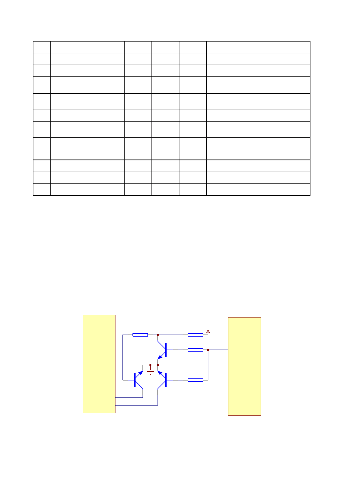
3.2.2CD/DVDswitchcircuit
1.CD/DVDswitchcircuitisshownasinthefollowingfigure3.2.2.1:
R103
10K
R104
10K
3904-S
R105
100K
Xs101
2SK3018-S
17
18
R102
100K
V101
VD101
VD102
2SK3018-S
Figure3.2.2.1CD/DVDswitchcircuit
AVCC
IOA
MT1389E
-15-
Page 20
2.Workingprinciple:afterdiscisloadedinmachine,IOAportisdefaultedhighleveltomakeVd102
saturationonandformloopwithCDlaserpowercontrolcircuitonloader,atthesametimeIOAalso
reachesloaderPDICforswitch,discbeginstorotate;whenservoprocessingsystemrecognisesthat
thediscinsidemachineisnotCD,IQApinoutputslowleveltomakeVd102cutoff,Vd101onandform
loopwithDVDlaserpowercontrolcircuitonloadertocarryouttheactionofreadingDVDdisc.After
doorisopened,IOAstillkeepsthestatebeforedoorisopened.Ifmachinecannotrecogniseswhichthe
discis,IQApinwillswitchalwaysuntilnodiscisreadoutorjudgedbysystem.
Note:V303,V304areMOSpipes(pressuredropissmallwhensaturationon).
3.2.3Laserpowercontrolcircuit
1.Laserpowercontrolcircuitisshownasinthefollowingfigure3.2.3.1:
LDO-AV33
R106
4.7R
23DVD
XS101
19CD
Figure3.2.3.1Laserpowercontrolcircuitdiagram
VD103
2SB1132-S
VD104
2SB1132-S
R107
4.7R
C106
106
LDO2
LDO1
C107
106
L104
601
LDO-AV33
DV33
22
20/21
MT1389
23
2.Workingprinciple:pin20/21ofMT1389islaserpowerdetectsignalinputpin,pin21isDVDlaser
powerstrong/weakdetectsignalinputpin,pin23isVCDlaserpowerdrivecontroloutputpin,pin22is
DVDlaserpowerdrivecontroloutputpin.
WhenreadingVCDdisc,laserpowerbecomesweak,voltageofMDIIpindecreases;whenvoltage
ofMT1389decreases,voltageofpin19ofXS101increasestoreachthefunctionofboostlaserpower;
whenlaserpoweristoostrong,voltageofMDIpinincreasestomakevoltageofMT1389increaseand
voltageofpin19ofXS101decreasetoreachthepurposeofloweringlaserpowertoformaautomatic
powercontrolcircuit.WhenreadingDVDdisc,pin21isdetectsignalinputpin,pin22isdrivecontrol
outputpinandtheworkingprincipleisthesamewiththatwhenplayingVCDdisc.
-16-
Page 21
3.2.4Mainaxiscontrolcircuit
1.Mainaxiscontrolcircuitisshownasinthefollowingfigure3.2.4.1:
C113
222
R108
680K
104/DNS
C114
OPO
R109
0R
ADIN
OPOP+
MT1389E
R111
DNS
R112
1R
R113
150K
C115
222
R114
680K
V1P4
6
5
4
3
2
1
XS102
PH-6
R110
150K
SPSP+
SL+
SL-
LIMIT
Figure3.2.4.1Mainaxiscontrolcircuitdiagram
2.Workingprinciple:MT1389Ehasacomparatorcomposedofoperationalamplifierinside.When
doorisopened,discisalwaysrotating,soabrakingsignalisrequiredtomakemainaxiselectric
machinestoprotatingimmediatelytorealizethepurposethatdisccanstoprotatingduringashort
periodafterdoorisopened.Inthecourseofplaying,if“OPEN”buttonispressed,mainaxisdrivesignal
disappears,butmainaxiselectricmachineisstillinrotatingstatebecauseofinertiafunction.The
inducedvoltageachievedbyinducedelectromotiveforceproducedbyelectricmachinerunningon
samplingresistorR321,R340,aftersamplingthroughresistorR112/R110/R113,inputtopin35,36of
MT1389,andoutputfrompin34afterMt1389amplifyingprocessinginside,afterD/Aconversionand
relevantprocessinginsideMt1389,aninstantelectricmachinereversebrakingsignalisoutputtedto
makemainaxiselectricmachinespeeddown.Thismachineismanualopen/closemeans,sodiscisstill
rotatingafterdoorisopenedbutitwillstopverysoon.
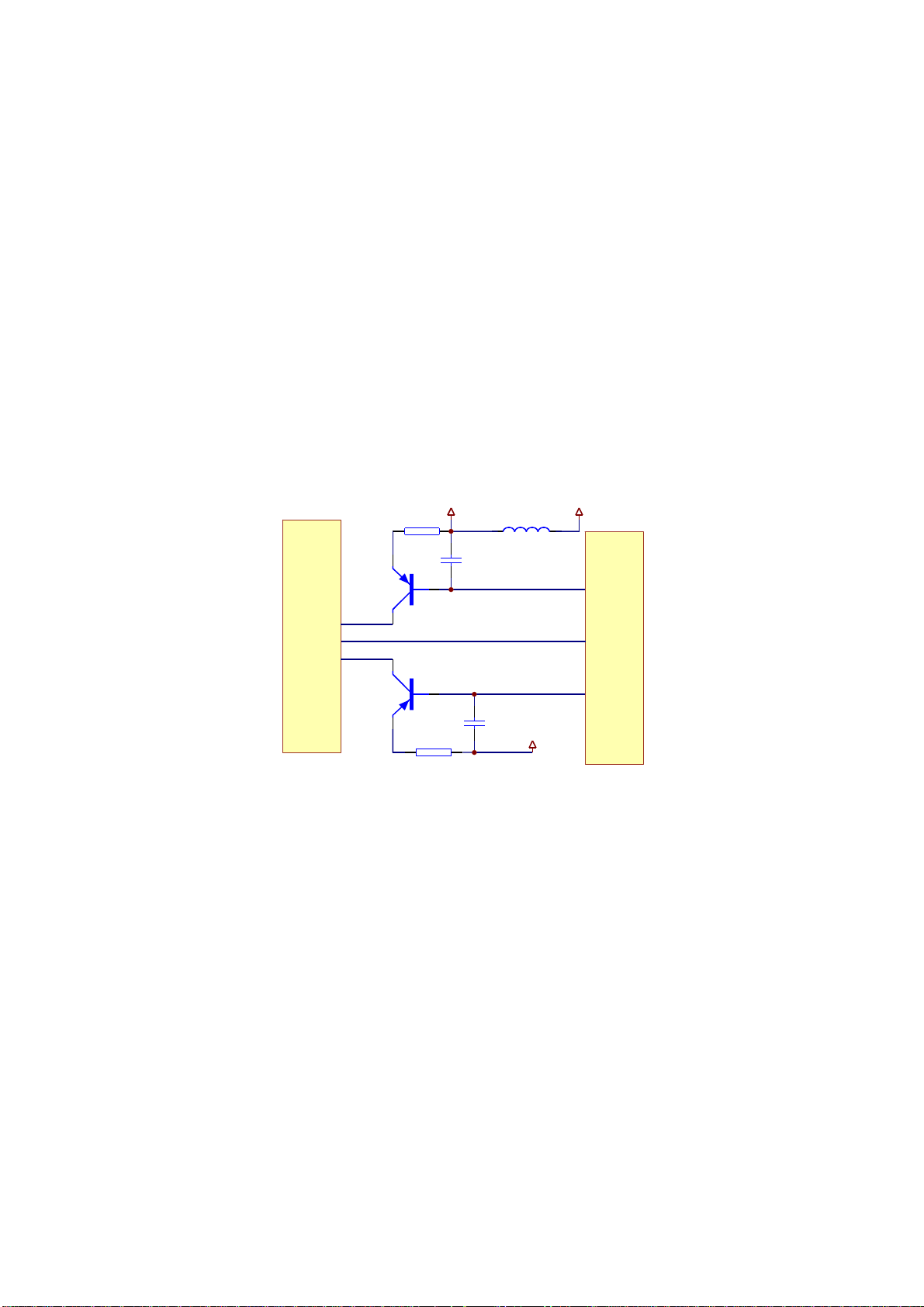
3.2.5DC-DCswitchcircuit
1.DC-DCswitchcircuitisshownasinthefollowingfigure3.2.5.1:
PGND
PGND
+9VIN
EN
1
SGND
2
3
4
5
6
7
8
9
10
11
12
13
14
15
16
17
35
CT2
COMP2
C906
SW2
68pF
IPK2
+9VIN
F+
FVCC
FOSO
R905
FMSO
10K
SL+
SL- SP+
R906
T- T+
10K
EN2
CT2
COMP2
SW2
IPK2
PVCC1
PVCC2
VOFC+
VOFCVCC1
VINFC
VINSL
MGND
VOSL+
VOSLMGND
VOTK+
MGND
AM5898N
COMP1
PGND2
PGND1
VOSP+
BIAS
MUTE
EN1
CT1
SW1
IPK1
PGND
VCC2
VINTK
VINSP
VOSP-
MGND
VOTKMGND
34
SBIAS
33
SELECT
32
31
30
COMP1
29
SW1
28
IPK1
27
26
25
24
VCC
23
TRSO
22
21
SP-
20
19
18
36
PGND
R1
10K
C907
68pF
DMSO
SW2
PGND
Figure3.2.5.1DC-DCswitchcircuitdiagram
R910
0R
1.2K
R911
750
R914
R913
680k
C908
102
R915
10K
R912
0.1
COMP2
QB902
AO3419
PGND
L902 47uH
1
D904
MBRS340
R916
3.6K
C909
104
2
100uF/16V
VCC
TC907
-17-
Page 22
2.Workingprinciple:whenswitchisclosed,AM5898islowlevel,DC-DCcircuithasno
EN1EN2of
function,machineisinpoweroffstate,butafterSw901isdisconnected,ENendishighlevel,DC-DC
circuitbeginstowork.TakeVCCforinstance,wegiveexplanationtovoltageregulatingofcircuit:
DC-DCcircuitbeginstooscillate,itsworkingfrequencyisin240khz,Swpinoutputson/offsignal.
WhengridelectrodeofQB902ishighlevel,MOSpipeison,+9VpowerreachesL902TC907through
MOSpipetosaveenergyforinductorandchargecapacitor,D904freewheelingdiode,whenMOSpipe
iscutoff,Ldischargesenergyanditsinducedelectromotiveforcemakesdiodeon,atthesametime
TC907dischargestheloadwithcurrentdirectionunchangedtoformaseriesconnectionswitchvoltage
regulatingcircuit.Whenoutputvoltageisonhighside,ithasthefollowingchanges:VCCincreases
COMP2increasesSW2on/offfrequencyturnslowVCCdecreases.Whenvoltageisonlowside,the
―
―
courseisoppositetothatofincrease.R912isover-currentprotectioncircuitsamplingresistor.(DV3.3
circuitprincipleisthesamewiththatofVCC)
Asshowninthefigure3.2.5.2,whenmachineisinDVD,SELECTpinofdecodechipoutputsahigh
leveltomakeservodrivecircuitenterworkingstateandreachVd1saturationonatthesametime,
VD901iscutoff,Qb904iscutoff,DCOUThasnopoweroutput.Whenmachineisswitchedtoexternal
input,SELECTpinofdecodechipoutputsalowleveltomakeservodrivercircuitnotwork,VD1iscutoff,
VD901issaturated,QB904issaturated,DCOUToutputsVCCtoprovideforTVbox.(CON3isDC
outputsocket)
JK901
1
2
3
CON3
VCC
R3
100R
R902
10K
QB904
AO3419
R903
0R
TC905
106
SELECT
R904
1K
Figure3.2.5.2DCOUTcontrolcircuit
VD1
3904
GND
VD901
3904
3.RelationshipofeachcontrolpinofAM5898
AM5898hasbuilt-inDCDCpowermanagerandcollaboratewithperipheralcircuittoprovideload
-
withtherequiredvoltage.Thiscircuitiswithover-voltageprotection,over-currentprotectionand
stabilityprotectionfunction,inwhichAM5898isalsowithservodrivefunction,whichhasbeen
introducedinservocircuitsection.Therelationshipofeachpinof
AM5898isshownasinthefollowing
table:
Truthtable(:active:inactive:dontcare)
○×-’
-18-
Page 23
MUTE EN1 EN2 MOTORCHANNEL DC-DCCTRL1 DC-DCCTRL2
H
—
— —
L L L × × ×
— — ○ — —
H
— — ○ —
H
— — ○
3.2.6Batteryvoltagedetectingcircuit
1.Batteryvoltagedetectingcircuitisshownasinthefollowingfigure3.2.6.1:
U502A
LM393
1
7
VCC
DV33
R509
4.7K
R510
4.7K
R511
33R
R512
33R
POWER_OFF
LOW_BAT
+9VIN
R504
27K
R505
1.2k
R506
18k
R507
47K
R508
47K
106
TC501
GND
6
5
L503
10UH
2
3
GND
U502B
LM393
Figure3.2.6.1Batteryvoltagedetectingcircuit
2.Workingprinciple:U502isanoperationalamplifierandusedasacomparatorincircuit.Reverse
inputterminalinputsaVCC5V,throughtworesistorspartialpressure,thereferencevoltage(2.5V)is
achieved;throughpartialpressurebyR504R505R506of
+9VIN,twogroupsofvoltageareachievedto
supplyforthein-phaseinputendofoperationalamplifier;whenvoltageofin-phaseinputendisless
2.5V,theoutputpinofoperationalamplifieroutputsalowleveltodecodechiptoperformthe
than
correspondingacts.Inthismachine,aftercalculation,weconcludethatwheninputvoltageislessthan
6.5V,pin7ofoperationalamplifieroutputslowlevelandmachinescreendisplayslowbattery;when
inputvoltageislessthan6.1V,pin1ofoperationalamplifieroutputslowlevelandmachinescarriesout
power-offaction.
-19-
Page 24
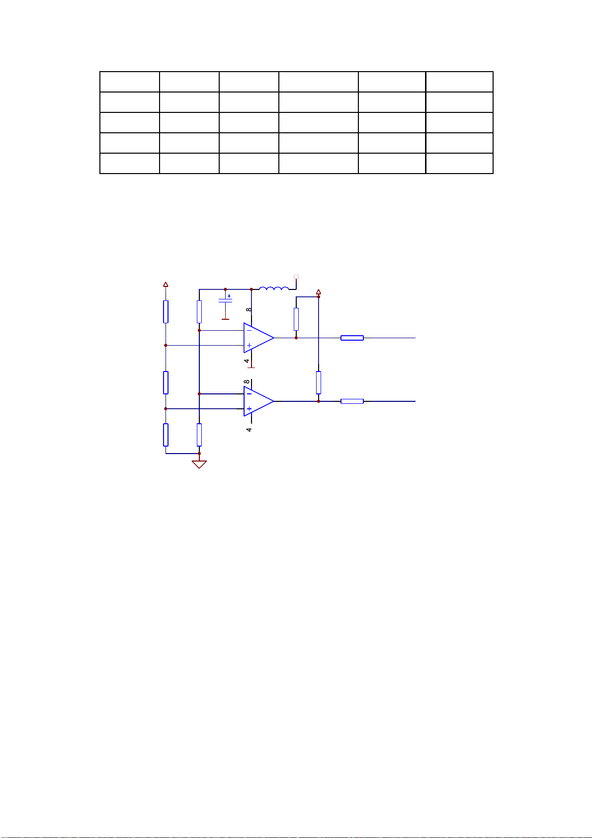
3.2.7Audiooutputcircuit
1.Audiooutputcircuitblockdiagramisshownasinthefollowingfigure3.2.7.1:
HP_L
HP_R
JK701
186
AL
LOUT
6
7
6
16
5
RSOUT-
U201
MT1389E
184
AR
U301
4558
ROUT
2
1
15
U701
LM4863
3
18
LSOUT-
LSOUT+
RSOUT+
Drive
board
JP3
ALIN ARIN
AUDIO_INJk301
Figure3.2.7.1Audiooutputcircuitblockdiagram
2.Workingprinciple:signalreadoutbydisc,throughaudioandvideodecoding,converseaudio
signalinMT1389Ebuilt-inDACcircuittoanalogaudiosignalandoutputleftandrightchannelanalog
signalsfrompin186,184ofMT1389E,throughTc301,Tc302,coupledtopin6,2ofU301andthen
outputfrompin1,7ofU301throughbeingfilteringandamplifyingbytheactivefiltercomposedofU301
andsendtoaudiooutputterminalandheadphoneamplifyingoutputcircuit.
(1)Headphoneamplifyingoutputcircuit
Asshowninthefigure3.2.7.2,aftervolumeadjustmentoftheaudiosignalsoutputtedfromU301
throughVR701,inputfrompin6,15ofU701respectively;audiosignalsafterbeingamplifiedoutput
frompin5,16ofU701toheadphonesocketforperformconversebetweenheadphoneandspeaker.
LOUT
ROUT
VR701
50K*2
R701
20K
C701 105
C702
105
R702
20K
R703
DNS
R704
DNS
R70536K
SPGND
C705
225
R706
36K
SP5V
C706
R712
104
1K
SPGND
TC703
100uF/16V
LM4863MTE
U701
R713
TC704
100uF/16V
100K
C707
104
SPGND
L701
TC701
100U/16V
HPL
R707
1K
SPGND
HPR
SP5V
10UH
GND
R709
R710
R711
100K
HP-V1
D701
1N4148
VCC
TC702
100U/16V
0R
0R
HP-L
HP-R
JK701
4
3
2
1
SPGND
HP
Figure3.2.7.2Headphoneamplifyingoutputcircuitdiagram
-20-
Page 25
(2)Outputmodeswitchinheadphoneandspeaker
LM4863drivespeakeradoptsbridgeconnection.Thatdrivesheadphoneissingleendingworking
modeanditsswitchbetweenthemisfulfilledbyHP-INpin.Asshowninthefigure3.2.7.2,when
headphoneisinsertedintoajack,a4V~VDDvoltageisaddedtoHP-IN,whichmaycutoffinternal
operationalamplifyingmoduleAmp2AandAmp2Btomaketheloadconnectedbybridgeinvalid.NowIC
liesinsingleendingworkingmodeandspeakerhasnosoundoutput.Whennoheadphoneisconnected
tojack,partialpressureresistanceofR711,R707makesthevoltagesuppliedtopinHP-IN(pin16)close
to50mV,driveAmp2AandAmp2Bareinworkingstatetomake4863workinbridgemodeandtransmit
tospeakerthroughdriveboardtomakespeakerhassoundoutput.
3.2.8Screenoffdetectcontrolcircuit
1.Screenoffdetectcontrolcircuitisshownasinthefollowingfigure3.2.8.1:
R602
10K
VCC
GND
R601
1K
SW601
SW2
升压板
BL_CTL
VCC
GND
8050
VD602
R604
1K
R605
1K
BL_CTL#
R603
1K
VD601
8050
Figure3.2.8.1Screenoffdetectcontrolcircuit
STBT
45
MT1389E
158
2.Workingprinciple:whenswitchisoff,pin45ofMT1389detectslevel,pin158outputslowlevelto
makeBL_CTLlowlevel,boostboardstopsworking;whenswitchisdisconnected,STBTishighlevel,
pin158ofMT1389outputshighleveltomakeBL_CTLhighlevel,boostboardbeginstoworkandlighten
backlightboard(whenswitchisinpanelposition,screencloseisoff,screenopenisdisconnected).
-21-
Page 26

3.2.9VideocodingandLCDTFTdrivecircuit-
1.VideocodingandLCDTFTdrivecircuitblockdiagramisshownasinthefollowingfigure3.2.9.1:-
U201
MT1389E
YUV0
YUV1
YUV2
YUV3
YUV4
YUV5
YUV6
YUV7
T102_RESET
MT1389_CLK
SDA/SCL
IOR
RGBsignal
IOG
amplifying
IOB
circuit
STV1
U801
STV2
T102
Externalvideoinput
Figure3.2.9.1VideocodingandLCDTFTdrivecircuitblockdiagram-
CKV
U/D
VCOM
OEV
L/R
OEH
STH1
STH2
CPH1
VR
VG
VB
Jp2
VCOMsignalamplifying
-10V
DC-DCconversion
Voltagedoubling
rectificationcircuit
Boostboardcomponents
Jp1
Driveboard
VGH
VGL
+15V
-10V
2.Workingprinciple:decodechipoutputsdigitalvideosignalanddirectlyinputstoT102forcoding
inthemeansofdatainparallel(8bit),andrestoredigitalsignalto3basecoloursignalthroughinternal
DACcircuitandareoutputtedbypin62,65,68andsenttoaamplifyingcircuitcomposedofsingletriode.
Shownasinthefigure3.2.9.2,conversesmallcurrentsignalofRGBintovoltageoutputmeanstodrive
LCDscreentodisplay.
VCOMsignalamplifyingcircuit:VCOM,afterU1(NJM2414)amplifying,outputsfrompin6,7to
displayscreenandisusedasthecolourfulfilteringplateof displayscreen.
BIAS
C845
104
+5VA
GND
IOR
R828
150
R831
39K
C841
106
Figure3.2.9.2Amplifyingcircuit
R834
10K
1
R840
100
GND
R837
430
C842
VD801
2N3904
R843
10K
106
C844
100pF
GND
C843
104
VR
-22-
Page 27
3.Voltagedoublingcircuit
Workingofdisplaydrivecircuitrequireshighvoltage,so+5Vvoltageisvoltagedoubled,shownas
inthefollowingfigure3.2.9.3:
D1
BAT54S
LX
C16
474
C17
474
3
3
D2
BAT54S
2
1
2
C20
C19
VOUT1
1
Figure3.2.9.3Voltagedoublingrectificationcircuit
C18
104
105
105
GND
R11
5.1K
C21
105
Q1
8050
D5
BZT52C16V
C22
106
C23
104
L5
560R
R15
10K
VGH
+5Vpower,throughDC-DCconversionconductedbyU2,istransmittedtothetwogroupsofvoltage
doublingrectificationcircuitcomposedofD1-D4toperformrectificationtopowersentfrompin1ofU2.
WhenLXinputisnegativehalfcircle,about-14VvoltageisformedincollectorelectrodeofQ2,-10VGL
voltageoutputtedafterD6voltageregulatingisprovidedtoVCOMsignalamplifyingcircuitanddisplay
screen.WhenLXinputispositivehalfcircle,thevoltagedoublingrectificationcircuitcomposedbyD1,
D2,C19cannotbeuptovoltagerequiredbyVGH,so7VDCcurrentachievedafterD7rectificationis
overlappedinpin1oftovoltageregulatingcircuitQ1,D5forvoltageregulatingandthenoutput+15V
DCpowertoprovidefordisplayscreen.+15VisoutputtedbyJP1todisplayscreenthroughsocketJP2
todriveboard.InwhichJP3ondriveboardmainlytransmitthesignalandpowerrequiredby
loudspeakerandboostboard.
4.Boostboard(ifthisPCBboardisdamaged,itwillnotbeservicedbutchangeitdirectly):howtojudgethe
boostboard:1)Makedetectingheadofoscillographclosetohighvoltageoutputline(payattentionnottotouchthe
line),asinewavewithabout60Kwillbeviewedfromoscillograph,whichmeansthatboostboardhasACoutput.
Themainfaultofboostboardisthatthereisnobacklightorbacklightisdark.
5.Functionintroductiontodisplayscreenpinisshownasinthefollowingtable:
Pin Symbol I/O description
1 GND - Ground
2 VCC P Power line for logic
3 VGL P Gate driver negative voltage
4 VGH P Gate driver positive voltage
5 STV1 I/O Gate driver START PULSE 1
6 STV2 I/O Gate driver START PULSE 2
-23-
Page 28
7 CKV I Gate driver scanning clock
8 U/D I Up/Down scanning change
9 OEV I Gate driver output enable
10 Vcom I
HORIZONTAL SYNCHRONIZATION SIGNAL(Voltage applied to color filter
substrate)
11 Vcom I Voltage applied to color filter substrate
12 L/R I Right / Left scanning change
13 MOD I Sampling mode change (H: Simultaneous, L: Sequential)
14 OEH I LATCH PULSE FOR COLUMN DRIVER
15 STH2 I/O Source scanning start signal 2
16 STH1 I/O Source scanning start signal 1
17 CPH1 I INPUT DATA CLOCK
18 CPH1 I INPUT DATA CLOCK
19 CPH1 I INPUT DATA CLOCK
20 Vcc P Power line for logic
21 GND P Ground
22 VR I Red video signal
23 VG I Green video signal
24 VB I Blue video signal
25 AVdd P Power
26 AVss P Ground
6.Scanningmodeselectionisshownasinthefollowingtable:
Scan control input setup
U/D L/R STVR STVL STHR STHL
GND Vcc O I O I
Vcc GND I O I O
GND GND O I I O
Vcc Vcc I O O I
Start up pulse I/O state
Scan mode
Up→down Left→right
Down→up Right→left
Up→down Right→left
Up→down Left→right
-24-
Page 29

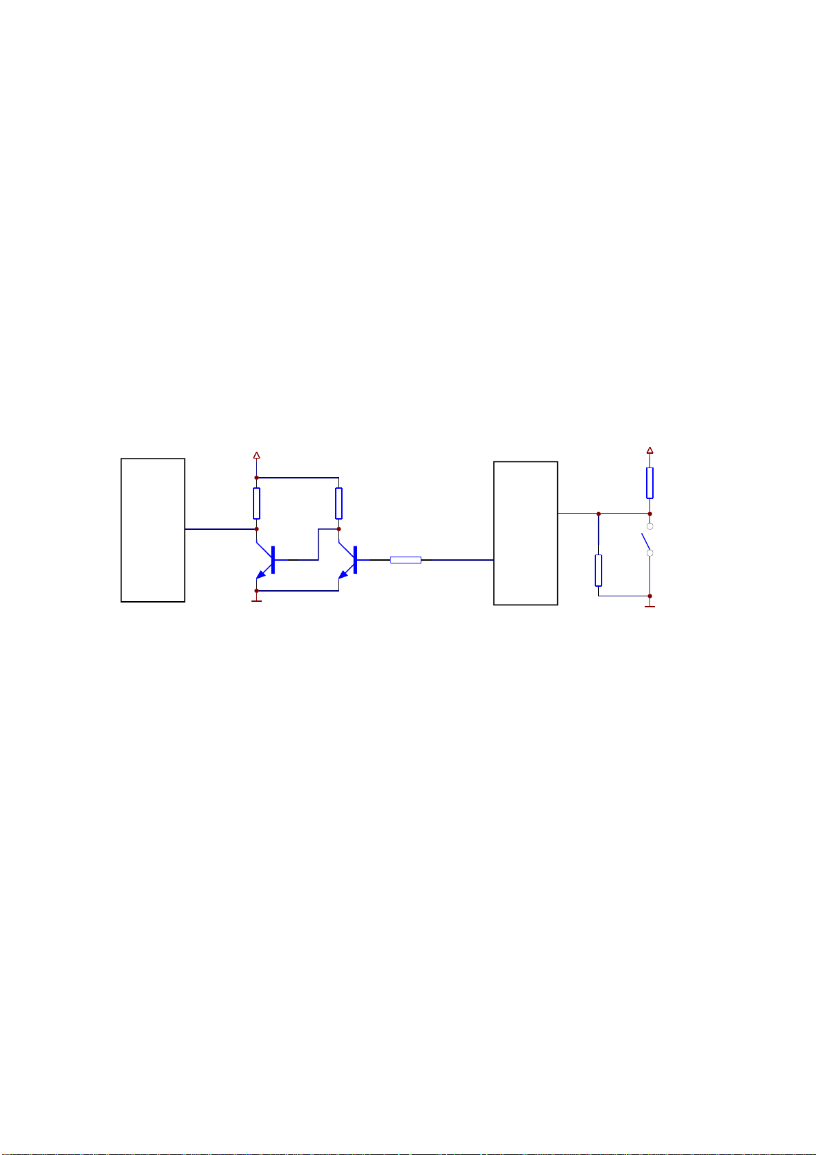
3.2.10Chargecircuitandprotectioncircuit
1.Battery:Lithium-ionpolymerchargeablebatteryalwaysfollowsthemethodofconstantcurrent
firstlyandthenconstantvoltage,andthenchargeinconstantvoltagestate.
2.Lithiumbatteryprotectionpart(thisPCBboardwillnotbeservicedinsidebatterycomponents)is
dividedintothreetypes:A)Over-voltageprotection,thatischargeprotection;B)Undervoltage
protection,thatisdischargeprotection;C)Currentprotection(shortcircuitprotectionincluded).The
protectiondelayanddelaytimeoftheabove3itemsaredifferent,from1secondto0.1secondandto
10mswithdelayadjustable.Twolithiumbatteriesprotection,nomatteovervoltageprotectionorunder
voltageprotection,theyaretherelationshipof“or”.Onlyoneofthetwocoreshasthecondition,the
protectionisavailable,whichrequiresthatthetwocoresofagroupofbatteryarebalancedonthewhole,
orelsethewholecapacitywillbeseverelydamaged(wheninovervoltageprotection,thecoreofhigh
voltagecausesovervoltageprotectionfirstly;wheninundervoltageprotection,thecoreoflowvoltage
causesprotectionfirstly).
3.Chargepart(chargeboardisaindividualPCBinsidemainunit):coreofchargepartissinglechip
thatadoptsA/Dconversionwith10-bit.8-bitsinglechip(S3F9454))ofPWM(12bits)SAMSUNG
companyhasthefollowingfeatures:
(1)Singlechipiswith10-bitA/Dconversionitself,theprecisionofA/Dconversionis1/1024,the
negativevoltageofgeneralNI-MHis3-6mv(6mv/1500mv=1/250),whichcanmeetthedemandsgreatly.
Theprecisionoflithiumbatterymaybeupto5mv.Consideringthetesterror,itmaybeupto20mv,
thatis4.2V+/-0.02v.Thehighprecisionandstrongpointareobvious.
(2)UsePWM(pulsewidthmodulator)ofsinglechipitselftodirectlycontrolDC/DCconversion.The
controlmethodisprovidedbysoftwaretoachievedifferentconstantcurrentandconstantvoltagecurve
(differentchargemeansmaybedesignedaccordingtoclients’requirements),sothewholelineissimple,
withlowcost,highreliability,highefficiencypowerconversionandlessheatradiation.
(3)MaychargeNI-MH,NI-CD,LI-IONbatterywell.Howtojudgewhetheritisfullycharged:A)max
voltage;B)maxtemperatureincrease;C)negativevoltage;D)longestchargetime.Itcanbetested
quicklyafterbatteryisfullychargedandloadedagain(within15minutes)andstopcharging(thispointis
veryimportanttoNIMHandNICD,whichcanpreventoverchargetodamagebattery),whenbattery
voltageislow,usesmallcurrenttochargetoresumethedamagedbattery.
±
4.Workingprinciple:whenexternalpoweradapterisadoptedtosupplypower,powerarrivesatVIN
pinthroughsocketboardandisdividedintotwoways:A)arriveatdecodeboard(VOUT+)directly
throughVD602;B)providedforchargecircuit.Aftervoltageregulating,thevoltageregulatingcircuit
composedbyV601,U602providesworkingvoltageforU601.U601ischargemanagementcontrol
singlechip.
-25-
Page 30

PowersupplyofCPUadoptsTl431andanNPNtriode.Therearemanyelements,butprecisionis
high,easytocorrectandupto1%,andtestworkisless.ThepowersupplycircuitiscomposedofU602
andV601,etc.
V605,V604,V603,QB602composeswitchDC/DCcircuit;V603andV604composestandardpush
pullcircuittodriveQB602tomakeQB602hasgoodswitchwaveformtodecreaseheatradiation.
QB602,L601,TC603andVD601composeclassicSTEPDOWNcircuit.WhenQB602ison,current
suppliespowerforbatteryononehandandsaveenergyforinductorontheotherhand.WhenisQB1cut
off,theelectric energyininductordischargesthroughVD601tochargebattery.
LM358isclassicin-phaseamplifyingcircuit.Thereasonofaddingamplifyingcircuitistodecrease
resistancetestandheatradiation.
ThefunctionofQB603istheexternalpowersupplycontrolend.WhenVINislowlevel,QB603ison,
batterysuppliespowerforload;whenVINishighlevel,adaptersuppliespowerforload.
QB601andV602composeprotectioncircuit.Whenchargecircuitorbatteryhastrouble,MOS_SW
outputshighlevel,QB601cutsoff,9Vstopssupplyingpowerforbattery.
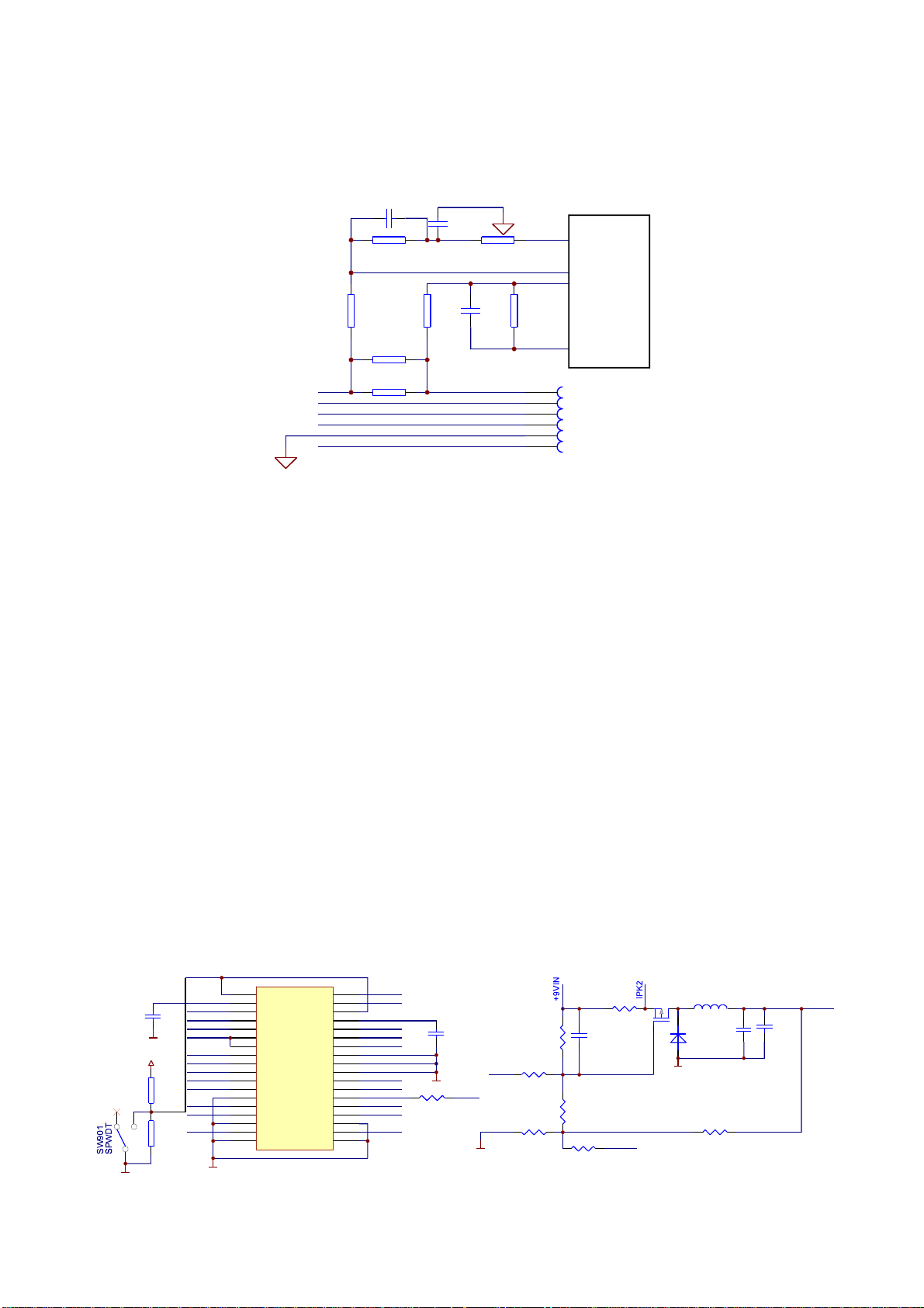
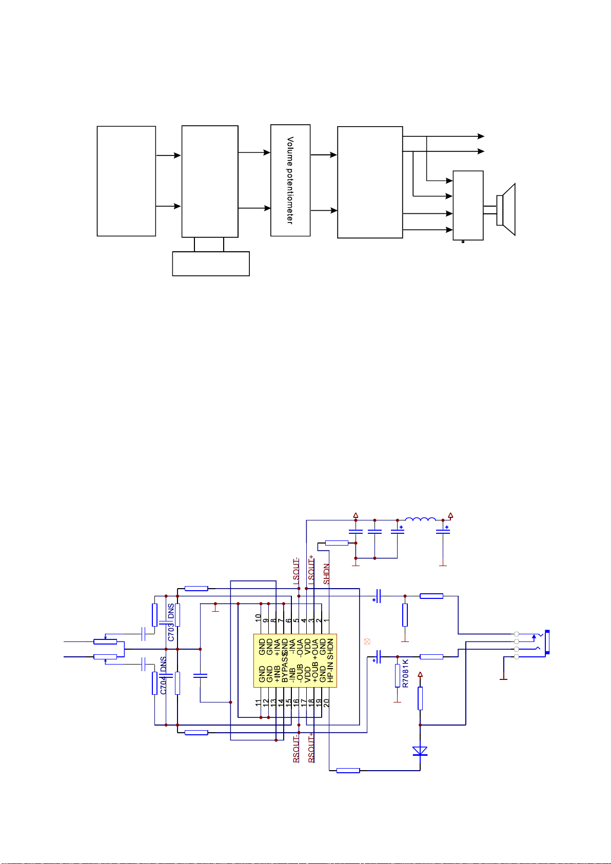
3.2.11Controlpanelcircuitandremotecontrolcircuit
PanelcontrolcircuitadoptsHT6222 controlcircuittocontrolanditsworkingpoweris3.3V.Afterwe
inputbuttonsinformation,serialdatasignalareachievedthroughHT6222internalprocessingandsent
todecodeboardthroughVSDApinandtoIRpin(102)ofdecodechipthroughaseparationdiodeVd201.
Thefunctionofseparationdiodeistopreventthemutualinterferenceofbuttonsfunctionandremote
controlfunctionandincorrectorderbeingcarriedout.
3.2.12Decodecircuit
1.Decodecircuitblockdiagramisshownasinthefollowingfigure3.2.12.1:
AL
AR
YUV0~YUV7
T102_RESET
MT1389_CLK
SDA/SCL
Audioamplifying
U301
27M
T102
U801
Loadercomponents
AM5898
Resetcircuit
FOSO
FMSO
TRSO
DMSO
URST#
101
186
184
MT1389E
93/94
U203
FLASH
Figure3.2.12.1Decodecircuitblockdiagram
U202
SDRAM
-26-
U204
24C02
Page 31

2.Workingprinciple:
(1)Power:MT1389iswithtwogroupsofpowersupply:onegroupachieves1.8Vvoltageafter
LM1117MP-1.8(U216)voltageregulatingtosupplyforthelogiccircuitinsideIC;theothergroup
achieves3.3VvoltageafterDC-DCconversionandQB903voltageregulating.Atthesametime,FLASH
andSDRAMmustalsomeettherequirementsofpower.
(2)Systemclock:clocksignalisanimportantfactorofmachine’sworking,thatwhetherthereis
clocksignalorwhetheritisnormalwillaffectthenormalworkingoftheplayer.Thismachineadopts
externalclock(27M)thatinputs topin194ofMT1389,clockisproducedbyT102anditsperipheral
circuit.
(3)Datacommunication
1)CommunicationofMt1389andSDRAM:thecommunicationofMT1389andSDRAMismainlyto
temporarilysavethelargequantitiesofdataafterMT1389decodingtoprepareforsavingatanytime.
Shownasinthefigure,DMA0DMA10isaddresssignal,DQ0DQ15isdatasignal,DCLKissynchronous
clock,DCKEisenabledend,CSischipselectionsignal,WEiswriteenabledsignal,RASandCASare
rowandlinegatingsignals.
DMA0—DMA10
DQ0—DQ15
158
145 21
MT1389
136
138
127
126
125
124
123/104
Figure3.2.12.2CommunicationblockdiagramofMT1389andSDRAM
MA11
#BA1
DCLK
DCKE
CS#
RAS#
CAS#
WE#
DQM0、 DQM1
35
38
37
19
18
17
16
15、39
SDRAM
2)CommunicationofMT1389andFLASH
ThecommunicationofMt1389andFLASHismainlytocalltheprogramandworkingdirections
savedinsideFLASHwhenpoweron.Shownasinthefigure,A0A19isaddressline,A20and21are
addressline,AD0AD14isdataline,DWR#isread-writecontrol,DCE#ischipselectionandDRD#isred
operation.
-27-
Page 32

A0—A19
AA20、21
AD0— AD14
MT1389
57
68
70
Figure3.2.12.3CommunicationblockdiagramofMt1389andFLASH
DWR#
DCE#
DRD#
FLASH
11
26
28
3.Audio,videooutput
(1)Video:MT1389integratesvideoencoderinside,soanalogvideosignalscanoutputfrom
Mt1389insidedirectly;butDL370Donlyneedtooutputdigitalsignal,anditsdigitalsignaloutputisas
follows:
Pin152~157andpin79/99ofMT1389EoutputMYUV0~MYUV78-bitdigitalvideosignalseparately.
(2)Audio:Mt1389integratesD/Aconversioninside,soanalogaudiosignaloutputfromMT1389
insidedirectly,anddigitalsignalmayalsooutputdirectlyandbeconversedbytheexternallyconnected
D/AconversionIC,whichisalsowithopticaloutputfunction.DL370Dadoptsanalogaudiooutputand
theoutputsignalsareasfollows:
◆◆
P187:ASLP186:AL
◆◆
P184:ARP183:ASR
◆◆
P182:ASUBWP188:ACENTER
◆
P159:DPDIF#
ThismachineonlyusestwochannelsofALandARandnootherchannels.
3.2.13Resetcircuit
1.Resetcircuitisshownasinthefollowingfigure3.2.13.1:
Dv33
+
D201
In4148
R212
K10
URST#
MT1389E
T102
R211
10K
Tc207
106
Figure3.2.13.1Resetcircuitdiagram
-28-
Page 33

2.Workingprinciple:afterpoweron,DV33chargesTC207throughR211.Voltageontwoendsof
capacitorcannotchangesuddenly,sopositivevoltageofTC207increasesgraduallyanditsincrease
timeisrelatedwithR211/TC207.Whenmachineisworkingnormally,thisvoltageisthesamewithpower
voltageonthewhole.Afterthiscircuitperformsresettodecodechip,pin95ofdecodechipoutputsa
resetsignaltopin28ofT102toperformresettoT102.Aftermachinepoweroff,theelectriccharge
savedinTC207dischargesthroughD201toensurethereliableresetafterpoweronnexttime.
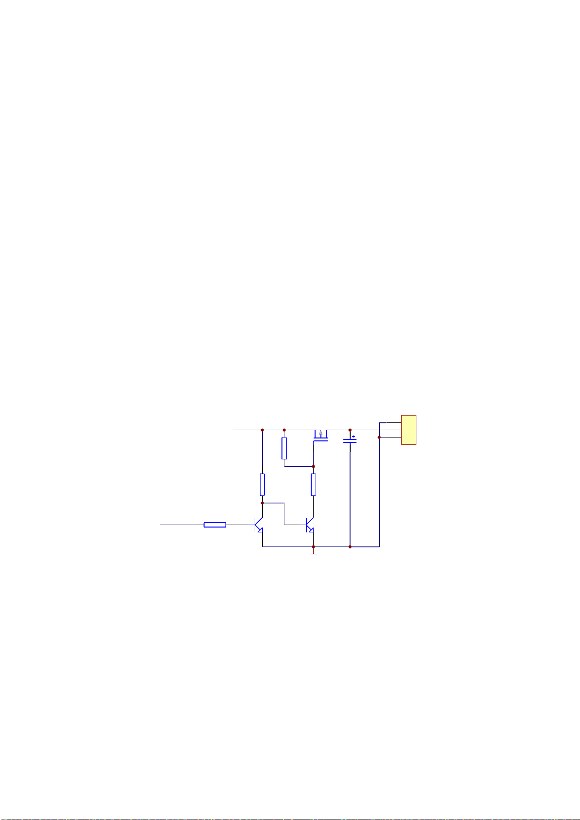
3.2.14Mutecircuit
1.Mutecircuitisshownasinthefollowingfigure3.2.14.1:
HP-L
MT1389E
MUTE_DAC
+9VIN
D301
1N4148
R321
1k
R323
1K
1
V304
8050
R322
10K
V303
8550
0
D302
1N4148
AGND
MUTE
R714
560R
R715
560R
R320
560R
V701
2SC1815-Y
SPGND
V702
2SC1815-Y
HP-R
LOUT
V301
2SC1815-Y
AGND
AGND
Figure3.2.14.1Mutecircuitdiagram
2.Workingprinciple:afterpoweron,+9Varrivesatthebaseelectrodeof
V702throughCEof
V303tomaketriodesaturatedon,audiosignaloutputandheadphoneoutputare
MUTE
R319
560R
V302
2SC1815-Y
V301,V302,V701,
ROUT
shortcircuitedtogroundtoremovenoisethatproduceswhenpoweron.Aftermachineresetsand
beginstoreaddisc,pin151ofMt1389outputsahighleveltomakepinMUTEchangefromhighlevelto
lowlevel,V301,V302,V701,V702arecutoffbecausethebaseelectrodeislowlevel,audiosignalcan
outputnormally.
-29-
Page 34

SectionServicingCases
3.3.1Servicinginstances
[Example1]Symptom:notreaddisc
Description:notreadanydisc
Analysisandtroubleshooting:firstly,pressdowndetectswitchofdoorandcheckwhetherloader
laserheadcanrestoretothemostinnercircleanditisnormalafterobserving.Thencheckwhetherlaser
headhasinfraredlightradiation,theintensityoflightradiation(payattentionnottostareatlaserlight
witheyesvertically,whichisharmfultoeyes,andlookatitatacertainangle)isbasicallynormal,then
loaddiscandobservetherotationspeedofdisc,thebeginningofrotationisbasicallynormal,andfinally
rotationspeedsupobviouslyandthelaserheadalsomovesalltheway,whichmeansthatitcannotfind
thediscinformation,firstlyyoumayconsiderthatlaserheadfocushastroubleandcannotfindthe
beginninginformation,changeloadercomponentsandtroubleisremoved.
[Example2]Symptom:noOSD
Description:machinecannotreaddisc,thereisnoimage
Analysisandtroubleshooting:firstlycheckpowersupplyofeachchannel,9V,3.3V,1.8V,5Vwhich
areallnormal,check5VofcontrollineBL_CTLofboostboardandbacklightvoltage9Vofboostboard
andboostboardoutput,whicharenormal;checkwhetherdetectswitchisstuckorwhetherdetectswitch
isinvalid,whicharenormal;checkCVBS0signalonL801andfindthatthereisno;checkpowersupply
ofMT1389,U202(SDRAM),U203(FLASH),U204(EEPROM),whichisnormal;checkpin1,24,25,48
ofFLASHaddressline(FLASHpinisdense,this4pinsareattheedge,soitiseasytomeasure)and
findthattherearetwopinswithoutwaveform,anothertwopinshavewaveformbutitisincorrect;after
changingFLASH,troubleisremoved.
[Example3]
Description:colourlossleadstothedistortionofplayedpicture
Analysisandtroubleshooting:playcolourfulbarsignalandfindthatgreensignalismissing;colour
lossisnotdisplayscreentroublegenerally,sofirstlycheckdisplaydrivecircuit,directlycheckamplifying
circuitofR,G,B,thereisIOGsignalbutthereisnooutputsignalVG;checktriodeVd802andfindthat
R835ismissedstuck,afterstickingitagainandtroubleisremoved.
[Example4]Symptom:whitescreen
Symptom:colourdistortion
Description:discreadingisnormal,soundisnormal,displayscreencannotdisplayimageandwhite
screenappears.
-30-
Page 35

Analysisandtroubleshooting:whitescreenmeansthatboostboardworkingisnormal,soitis
preliminarilyjudgedthatdisplaydrivehastrouble,checkvoltageof3.3V,2.5VofU801andtheyareboth
normal;checkinput/outputsignalCVBS0,SDL,SCL,YUV,STH,VCOM0andfindthatthereisno
VCOM0signal;afterchangingU801,thetroubleisremoved.
[Example5]Symptom:headphonehasnooutput
Description:loudspeakerandheadphonebothhavenooutput.
Analysisandtroubleshooting:useoscillographtotestwhetherthereissoundsignalthatoutputsto
headphoneterminal,andthereisno;testwhetherleftandrightofTC703,TC704electrolyticcapacitor
havewaveformoutputandthereisno;checkwhethermutecircuitisnormal,MUTEsignalislowlevel,
normal;checkpin15,16ofU701(LM4863headphone/loudspeakerdrive),andthereissoundsignal
input;afterchangingU701,troubleisremoved.
[Example6]Symptom:powernoton
Description:machinehasnoresponseafterpoweron
Analysisandtroubleshooting:checkwhether9Vvoltagecomesthroughchargeboardanditis
normal;checkQB902,QB903,andthereis5V,3.3Vconversion,whichisnormal;checkpowersupplyof
eachchannelandfindthatL216hasno1.8Voutput,soitisdoubtedthatU206hastrouble;after
changingU206,troubleisremoved.
[Example7]Symptom:afterinstallingbattery,unplugpoweradapter,screenwillbedarkfor1-2Sand
thenbecomenormal.
Description:usebatterytosupplypower,unplugpoweradapter,screenwillbedarkfor1-2Sand
thenbecomenormal.
Analysisandtroubleshooting:firstlycomparedefectivemachinewithgoodone,goodonewillflash
once,butitflashesslightlyandshortly,andyouwillnotbeawareifyoudonotobservecarefully;
becausethebrightnessanddarknessofscreenhascloselyrelationtoboostboard,firstlycheckboost
board;accordingtoexperiences,iftheR9rosinjointonboostboardwillleadtodarkscreen,use
multimetertotestandthereisnorosinjoint,useoscillographtotouchHV,LVsignal,andunplugpower
adapteratthesametime,troubledoesnotappearagain,useman-madesimulatingmethodtoinsert
andunplugquicklyandtroubleappearsagain,sinewaveonoscillographdisappearsfor1-2s,check
BL_9VpowersupplyandfindthatduringtroubleperiodBL_9Vvoltagewillhavedistortion(itisalittle
similartodistortionsinewave,butmuchmorecomplicated),takedownICanddistortionstillexists,
whichmeansthatitisnotICfault,checkelementconnectedwithBL_9V,whentestingtopin11ofIC,we
findthatduringthefaultperiodof9Vvoltage,thereisdistortionwaveform,afterchangingC7,troubleis
removed.
[Example8]Symptom:notreaddisc
Description:notreadanydisc
Analysisandtroubleshooting:firstlypressdownopendetectingswitchandobservelaserhead
focusandheatradiation,whicharenormal;afterchanginglaserhead,troublestillexists;loaddiscand
-31-
Page 36

Readit,whenlaserheadbeginstofocus,laserheadcannotbesearchedandslidesbackandforth,use
oscillographtocheckfocusandtracesignalandtheyareallnoisywave,checkthedigitalsignalatfront
endofintegration,itisstillnoisywave;checkA,B,C,D,Thereforesignalandtheyarealsonoisywave,
checkthepathbetweenthemandthereisnoproblem,eachcapacitorhasnorosinjointandjoint
welding;whencheckingwhetherflatcableholderXS101hasrosinjoint,tinseemstobeconnected
betweenpin8,9;usemultimetertotestandthereisactuallyshortcircuit,afterremovingweldingtin,
troubleisremoved.
[Example9]Symptom:noiseexistswhenplaying
Description:thereisnoisewhenplayingnotanydiscs,loudspeakerandheadphonebothhave
noise.
Analysisandtroubleshooting:firstlymakeclearthatitisloudspeakertroubleorothercircuittrouble,
useheadphonetolistentoJk701andcheckwhetherithasnoise,ifithas,itisconfirmedthatcircuithas
trouble,thenplay1KHZstandardsignaldisc,itiseasytotestwaveform,useoscillographtocheckpin3
and18waveformofU701,itshouldbesinewave,butthereisnoisywavetoappearconsequently,then
checkpin5and15ofU701,inputpinofleft/rightchannel,andthereisstillnoisyweavetoappear,goon
checkingtothefrontstage,checkC701,C702waveformandthereisstillnoisywavetoappear;directly
testpin1and7ofU301,andthereisstillnoisywave,thencheckpin2and6ofU301,andwaveformis
normalconsequently,testpowersupplyofU301,itisalsonormal;afterchangingU301,troubleis
removed.
[Example10]Symptom:blackscreen
Description:screenofmachinehasnodisplayafterpoweron
Analysisandtroubleshooting:firstlycheckwhetherpowerindicatorlightemitslighttojudgewhether
powerstartsup;ifindicatorlightisnormal,loaddiscandcheckwhetherdiscreadingcancontinueand
whetherdiscreadingisnormal;listenloudspeakerandcheckwhetheritssoundisnormal,ifitisnormal,
thepowerisjudgedtobenormalpreliminarily.Thenpressscreendisplaydetectswitchtocheckwhether
screendisplayhaslightflashing,ifthereisno,check5VofdetectsignalcontrollineBL_CTLofboost
boardandbacklightvoltage9Vofboostboardandboostboardoutputandtheyareallnormal;thentest
whetherhighvoltagehasoutput.Usedetectingheadofoscillographtocloseuphighvoltagelineof
inputdisplayscreenandthereshouldbesinewave.Finallychangedisplayscreenandtroubleis
removed.
ExampleSymptom:nooutput
[11]
Description:machinescreenhasnodisplayafterpoweron,cannotreaddisc.
Analysisandtroubleshooting:firstlytest3.3V,1.8VvoltageafterDC-DCconversion,voltageoutput
isnormal,thentestwhethercrystaloscillatorY801hasoscillation,anditisnormal,andfrequency
27.00MHZisalsonormal,thentestURST#resetvoltage3.0Vanditisalsonormalbasically,thentest
softwaredata128Manditalsonormal,thentestU202DCLK,DCKEandithasresponse,andonly
addresslinehasnoresponse,sowebegintodoubtthatSDRAMhastrouble,changeitandthereisstill
-32-
Page 37

Nooutput,finallywedoubtthatchipMt1389hastrouble;afterchangingMT1389,troubleisremoved.
[Example12]Symptom:noiseappearswhenplayingCD
Description:itisnormalwhenplayingotherdiscs,butnoiseappearswhenplayingCDdisc
Analysisandtroubleshooting:firstlymakeclearwhetherotherdiscshavenoise,playDvddiscand
testthatthereisnonoise,thenlistentoheadphoneandcheckwhetherithasnoisetoconfirmwhetherit
isloudspeakertroubleorheadphonetrouble,andtheybothhasnoiseconsequently;nowweanalyse
thatDVDisnormal,whichmeansthatDACaudiodecodeandoperationalamplifierarebasicallynormal,
thenprocessaudiodecodeanddatahastrouble,whichismainlycausedbySDRAManddecodechip,
changeSDRAManditisinvalid,thenchangedecodechipMT1389andtroubleisremoved.
[Example13]Symptom:notreadCDdisc
Description:DVDdiscreadingisnormal,CdandVCDdiscreadingarenotavailable
Analysisandtroubleshooting:DVDdiscreadingisnormal,soitisjudgedthatfocusandtraceis
normalbasically;firstlywedoubtwhetherdetectinghaserror,testIOAvoltageofpin44ofMT1389,and
thevoltageatthattimeisabout3.1whichisobviouslyincorrect,whenreadingDVDdisc,itishighlevel,
nowVCDdiscisbeingreadanditisalsohighlevel,triodeV102willnotbeonatall,ofcourseloader
laserheadCDlaserpipewillnotbelightened;directlychangeMT1389andtroubleisremoved.
[Example14]Symptom:notreaddisc
Description:notreadanydisc
Analysisandtroubleshooting:laserheadisinmiddleandcannotreturntothemostinnercircleafter
poweron,firstlymeasureT+,T-voltageanditisabout2.5V,whichisbasicallynormal,thentestfeed
innerresistanceonloadercomponents,itisabout8ohm,whichisalsonormal,finallycarefullyobserve
Xs102flatcableholderandfindthatthereisoneflatcableofthe6loaderflatcablethatfallsoff,after
pressingtightly,troubleisremoved(thisloaderalwayshasthistrouble,whichshowsthatmainaxis
electricmachinedoesnotrotatesometimesandalsopayattentiontoobservethisplug).
[Example15]Symptom:whitescreen
Description:TFTscreenappearswhitescreen,nonormalimageoutput
Analysisandtroubleshooting:boostboardisnormalanditispreliminarilyjudgedthatdisplaydrive
parthastrouble,checkeachvoltage3.3V,2.5VofU801andtheyarebothnormal;testoscillationof
Y801anditisnormal;testtricolouranditisnormal;test8-bitdataanditisnormal,whichmeansthat
U801workingisnormal,changedisplayscreenandtroublestillexists.Thenwedoubtthatitisthe
displayscreenflatcableholderthathastrouble,observecarefullyandfindthat3.3Vpowersupplypinof
flatcableholderDV333.3Vhasfalsewelding;afterweldingagainandtroubleisremoved.
-33-
Page 38

3.3.2Troubleshootingflowchart
1.Troubleshootingflowchartfor“Notreaddisc”isshownasinthefollowingfigure3.3.2.1:
Notreaddisc
Whether
laserheadhasresets
Y
Whether
thereisfocusaction
Y
N
pin12ofAM5898has
whethervoltage
ontwoendsofelectric
N
pin11ofAM5898
whethervoltageof
pin8,9ofAm5898is
Whether
feedsignal
input
Y
Check
machineis
equal
Y
CheckAM5898
Whether
hasfocussignal
input
Y
Check
normal
N
CheckMT1389andC231
N
Checkelectricmachine
N
CheckMT1389andC233
N
CheckAM5898
Whether
mainaxiselectric
machinerotates
Y
A
Checkthelinebetween
pin1,2ofXS101andcoil
N
Whether
pin22ofAm5898has
signalinput
Check
whethervoltageof
pin21,22ofAM5898
isnormal
Checkelectricmachine
Y
N
CheckMT1389andC230
Y
N
Y
CheckAM5898
-34-
Page 39

A
Whether
laserheademitslight
Y
Whether
rotationspeedofdiscis
normal
N
N
Check
whetherAPCcircuit
providesvoltagefor
laserhead
Y
Changeloader
Whether
thereisRFsignal
N
N
Check
whetherLDO_DV33
isnormal
Y
Check
whetherLD01isnormal
Y
Check
V104,V103andsocket
XS101
Y
Change24Pflatcable
Changeloader
N
N
Check
powersupplycircuit
Y
CheckMT1389
Change
Y
Changeloader
Y
Whether
thereareABCDEF
signal
Y
CheckMT1389andperipheral
N
CheckXS101andflatcable
Figure3.3.2.1Troubleshootingflowchartfor“Notreaddisc”
-35-
Page 40

2.Troubleshootingflowchartfor“Playerhasnooutput”isshownasinthefollowingfigure3.3.2.2:
Playerhasnooutput
Whetherresetisnormal
Y
Whether
thereis27Mclock
Y
Whether
1.8Vpowersupplyis
normal
Y
Check
whetherpower
supplyofdecodechip,
FLASH,DRAM
isnormal
N
Checkresetcapacitor
N
CheckT102andcrystal
oscillator
N N
CheckthelinefromL216
todecodeIC
N
Checkpowersupplycircuit
Check
whetherpin3
ofU206has3.3V
powersupply
Y
Whether
pin2ofU206has
1.8Voutput
Y
Serviceaccordingto
troubleshootingprocess
for“No3.3V”
N N
Whether
V18isshort
circuitedtoground
Y
CheckMT1.89and1.8V
filteringcapacitor
ChangeU206
ChangeSDRAMorMT1389
Y
Check
whetherclock
ofpin38ofSDRAM
isnormal
Y
B
Weldagain
N N
WhetherDCLKis27M
Y
Check
whetherFLASHis
normal
Y
Y
Check
whetherMT1389is
rosinjoint
-36-
N
Check
whetherSDRAM
isrosinjoint
Y
Weldagain
N
N
ChangeFLASH
ChangeMT1389
N
Check
whetherdecode
chipisrosinjoint
Y
Weldagain
Page 41

B
Check
whetherFLASH
hasdataoutput
Y
Check
whetherSDRAM
datalinehas
signal
Y
Check
whetherU204is
normal
Y
Checkthelinebetween
decodechipandFLASH/DRAM
N N
N
N
Check
whetherFLASH,
Mt1389hasrosin
joint
Y
Weldagain
Check
whetherFLASH,
Mt1389hasrosin
joint
Y
Weldagain
ChangeU204
ChangeFLASHorMT1389
N
ChangeFLASHorMT1389
Figure3.3.2.2Troubleshootingflowchartfor“Playerhasnooutput”
-37-
Page 42

3. Troubleshootingflowchartfor“NoVCCvoltage”isshownasinthefollowingfigure3.3.2.3:
NoVCCvoltage
Check
whetherresistance
ofVCCpintoground
isnormal
Y
Check
whetherR910has4V
voltage
Y
Check
whetherthe
endconnectedtoQB902
ofR912has9V
voltage
Y
Check
whethercathode
ofD904has5V
voltage
Y
N
N
N
N
Checkloadcircuit
ChangeAM5898N
CheckR912
ChangeQB902
Check
whetherL902
hasopencircuit
Y
Change
N
CheckwhetherTC907has
electricityleakage
Figure3.3.2.3Troubleshootingflowchartfor“NoVCCvoltage”
-38-
Page 43

4.Troubleshootingflowchartfor“NoDV33Vvoltage”isshownasinthefollowingfigure3.3.2.4:
NoDV33Vvoltage
Check
whetherresistance
togroundofDv33is
normal
Y
Check
whetherR917
has5.5Vvoltage
Y
Check
whetherthe
endconnectedtoQB903
ofR917has9V
voltage
Y
Check
whethercathode
ofD904has5V
voltage
Y
N
N
N
N
Checkloadcircuit
ChangeAM5898N
CheckR912
ChangeQB902
Check
whetherL903
hasopencircuit
Y
Change
N
CheckwhetherTC909
haselectricityleakage
Figure3.3.2.4Troubleshootingflowchartfor“NoDV33Vvoltage”
-39-
Page 44

5.Troubleshootingflowchartfor“NoVCC,DV33Vvoltage”isshownasinthefollowingfigure
3.3.2.5:
NoVCC,DV33
Whether
+9VINisnormal
Y
Whether
pin1ofAM5898
ishighlevel
Y
ChangeAM5898
N
Check+9Vfilteringcapacitor
andpowersupplyline
N
SetswitchinOFFposition
Check
whetherpower
adapterofchargeboard
isnormal
Y
Whether
+9VDcsocketis
normal
Y
Whether
SW901isinOFF
position
Y
N
Poweradaptertroubleshooting
N
N
Change
ChangeSW901
Figure3.3.2.5Troubleshootingflowchartfor“NoVCC,DV33Vvoltage”
-40-
Page 45

6.Troubleshootingflowchartfor“Audiohasnooutput”isshownasinthefollowingfigure3.3.2.6:
Audiohasnooutput
Whether
headphonehassound
Y
N
whetherMUTEislow
Check
level
ChangeMT1389
N
N
Y
Check
whetherMUTE_DAC
ishighlevel
Y
Check
whetherV304is
normal
Check
whetherV303isnormal
Y
CheckR714/R715
N
N
N
Check
whetherthereismute
Y
Cancelmute
ChangeV304
ChangeV303
Whether
pin20ofU701is4V
Y
Check
whetherloudspeakeris
normal
Y
ChangeU701
15ofU701hassignal
N
Headphonesocketis
notgood
N
Changeloudspeaker
Check
whetherpin6,
input
Y
ChangeU701
N
CheckA9Vpowersupply
circuit
Check
whetherpotentiometer
hassignal
whetherpotentiometer
isnormal
Checkelementfrom
potentiometertoU701
ChangeMT1389
input
Y
Check
Y
N
CheckthelinefromU301
topotentiometer
N
N
N
Check
whetherU301has
signaloutput
Changepotentiometer
Check
whetherU301
hassignalinput
Check
whetherpower
supplyofU301is
normal
N
Y
Y
Figure3.3.2.6Troubleshootingflowchartfor“Noaudiooutput”
-41-
Y
CheckU301
Page 46

LCDdisplaytrouble
Whether
LCDhasbacklight
output
Y
Whether
thereisimageoutput
Y
N
N
whetherboost
boardhashighvoltage
Checkwhetherdisplay
screenisnormal
whetherYUV
hassignalinput
Check
output
Check
N N N
Y
N N
Y
Check
whetherpin2ofJp6
ishighlevel
Y Y
Changeboostboard
Check
whether27Mclockis
normal
Y
Check
whetherdecodeboard
worksnormally
Y
ChangeMT1389
Check
whetherVD602is0.7V
CheckVD602/VD601
Check
27Mcrystal
oscillationandmatched
capacitor
Y
CheckT102powersupply
N
Decodecircuittroubleshooting
N
Check
whetherSTBTishigh
level
Y
ChangeMT1389
Change
N
ChangeSW601
C1
Check
whetherIOG,
IOB,IORhassignal
output
Y
C2
Check
N
whetherreset
andpowersupplyof
T102isnormal
Y
ChangeT102
N
Removeonebyone
Page 47

C2
C1
Check
whetherVG,
VR,VBhassignal
output
Y
Check
whetherdrive
boardVR,VG,VBhas
signal
Y
Check
whetherVGH,
VGL,+5Vvoltageon
driveboardis
normal
Y
Checkdisplayscreen
socketanddisplayscreen
N
CheckRGBamplifyingcircuit
N
N
Checkvoltageregulating
circuit
Check
XS801andflatcable
Y
Check
whetherthereisrosin
joint
Check
whetherLX
waveformofDC-DC
circuitis
normal
Y
N
N
N
Change
Weldagain
ChangeU2
Whether
pictureoutputis
normal
Y
Whether
colourisnormal
N
Checksignalpathwayand
displayscreen
N
Check
whetherVCOMsignal
isnormal
Check
whetherother
displaydrivesignal
isnormal
Check
whether27Mclockis
normal
Check
whetherT102is
normal
N
CheckU1anditsperipheral
Y
N
Y
N
Y
N
ChangeT102
Checkcrystaloscillatorand
externallyconnectedcapacitor
Change
Y
CheckwhetherMT1389is
normal
Figure3.3.2.7Troubleshootingflowchartfor“LCDdisplaytrouble”
-43-
Page 48

SectionFourServicingParameters
3.4.1Signalwaveformdiagram
Thissectioncollectssignalwaveformdiagramofaudio,videoandeachunitcircuitwiththepurpose
tohelpservicingpersonneltojudgewheretroubleliesinaccuratelyandquicklytoimproveservicing
skills.Forthedifferenceofoscillograph'stype,modelandtuner,acertaindifferencemayexist,sothe
servicingpersonnelareexpectedtopaymoreattentiontocheckindailyoperation.
1.Waveformdiagramofpin28MofchargeboardU601
2.Waveformdiagramofpin4CKVofJP2
-44-
Page 49

3.WaveformdiagramofmainaxisdriveDMOoutputtedbydecodechip
4.WaveformdiagramofFOoutputtedbydecodechip
5.WaveformdiagramofFMoutputtedbydecodechip
-45-
Page 50

6.WaveformdiagramofTRoutputtedbydecodechip
7.WaveformdiagramofLXsignalofpin1ofG5105
8.WaveformdiagramofCLKofpin194ofMT1389
-46-
Page 51

9.WaveformdiagramofOEHofpin11ofJP2
10.WaveformdiagramofSTH1,STH2ofpin12,13ofJP2
11.Waveformdiagramofpin5,6STV1,STV2ofJP2
-47-
Page 52

12.Waveformdiagramofpin29SW1ofAM5898
13.Waveformdiagramofpin4SW2ofAM5898
14.Waveformdiagramofpin13ofU601
-48-
Page 53

15.Waveformdiagramofpin7VCOMOofJP2
16.Waveformdiagramofpin17VRofJP2
17.Waveformdiagramofpin81~88YUVofT102
-49-
Page 54

18.Waveformdiagramofblacklightdrivevoltage
Note:backlightdrivevoltageishigh,whentesting,detectingheadofoscillographcannotbe
contactedwithoutputterminaldirectly,onlyclosetooutputterminalandwaveformcanbetested.
19.URSTwaveformdiagram
20.Waveformdiagramofpin6U1VCOM
-50-
Page 55

Section Five Function Introduction to IC
3.5.1 function introduction to MT1389E
1. DESCRIPTION
MT1389E is a cost-effective DVD system-on-chip (SOC) which incorporates advanced features like
MPEG-4 video decoder, high quality TV encoder and state-of-art de-interlace processing.
Based on MediaTek’s world-leading DVD player SOC architecture, the MT1389E is the 3rd generation of
the DVD player SOC. It integrates the MediaTek 2nd generation front-end analog RF amplifier and the
Servo/MPEG AV decoder.
To enrich the feature of DVD player, the MT1389 equips a simplified MPEG-4 advanced simple profile
(ASP) video decoder to fully support the DivX1 Home Theater profile. It makes the MT1389-based DVD
player be capable of playback MPEG-4 content which become more and more popular.
The progressive scan of the MT1389E utilized advanced motion-adaptive de-interlace algorithm to
achieve the best movie/video playback. It also supports a 3:2 pull down algorithm to give the best film effect.
The 108MHz/12-bit video DAC provides users a whole new viewing experience.
2. Key Features
RF/Servo/MPEG Integration
Embedded 6ch Audio DAC
Embedded 2ch Audio ADC for Karaoke
High Performance Audio Processor
High Performance Progressive Video Processor
Support Nero-Digital
High Quality 108MHz/12-bit, 4 CH TV Encoder
3. General Feature lists
(1)Integration DVD player single chip
High performance analog RF amplifier
Servo controller and data channel processing
MPEG-1/MPEG-2/JPEG video
Dolby AC-3/DTS Decoder
Unified memory architecture
- 51 -
Page 56

Versatile video scaling & quality enhancement
OSD & Sub-picture
Built-in clock generator
Built-in high quality TV encoder
Built-in progressive video processor
Audio effect post-processor
Built-in 5.1-ch Audio DAC
Built-in 2-ch Audio ADC for Karaoke
(2)High Performance Analog RF Amplifier
Programmable fc
Dual automatic laser power control
Defect and blank detection
RF level signal generator
(3)Speed Performance on Servo/Channel Decoding
DVD-ROM up to 4XS
CD-ROM up to 24XS
(4)Channel Data Processor
Digital data slicer for small jitter capability
Built-in high performance data PLL for channel data demodulation
EFM/EFM+ data demodulation
Enhanced channel data frame sync protection & DVD-ROM sector sync protection
(5)Servo Control and Spindle Motor Control
Programmable frequency error gain and phase error gain of spindle PLL to control spindle motor on CLV
and CAV mode
Built-in ADCs and DACs for digital servo control
Provide 2 general PWM
Tray control can be PWM output or digital output
(6)Embedded Micro controller
Built-in 8032 micro controller
Built-in internal 373 and 8-bit programmable lower address port
1024-bytes on-chip RAM
Up to 2M bytes FLASH-programming interface
- 52 -
Page 57

Supports 5/3.3-Volt. FLASH interface
Supports power-down mode
Supports additional serial port
(7)DVD-ROM/CD-ROM Decoding Logic
High-speed ECC logic capable of correcting one error per each P-codeword or Q-codeword
Automatic sector Mode and Form detection
Automatic sector Header verification
Decoder Error Notification Interrupt that signals various decoder errors
Provide error correction acceleration
(8)Buffer Memory Controller
Supports 16Mb/32Mb/64Mb SDRAM
Supports 16-bit SDRAM data bus
Provides the self-refresh mode SDRAM
Block-based sector addressing
(9)Video Decode
Decodes MPEG1 video and MPEG2 main level, main profile video (720/480 and 720x576)
Decodes MPEG-4 Advanced Simple Profile
Support DivX 3.11/4.x/5.x Home Theater Profile
Support Nero-Digital
Smooth digest view function with I, P and B picture decoding
Baseline, extended-sequential and progressive JPEG image decoding
Support CD-G titles
(10)Video/OSD/SPU/HLI Processor
Arbitrary ratio vertical/horizontal scaling of video, from 0.25X to 256X
65535/256/16/4/2-color bitmap format OSD,
256/16 color RLC format OSD
Automatic scrolling of OSD image
(11)Audio Effect Processing
Dolby Digital (AC-3)/EX decoding
DTS/DTS-ES decoding
MPEG-1 layer 1/layer 2 audio decoding
MPEG-2 layer1/layer2 2-channel audio
- 53 -
Page 58

High Definition Compatible Digital (HDCD)
Windows Media Audio (WMA)
Dolby ProLogic II
Concurrent multi-channel and downmix out
IEC 60958/61937 output
PCM / bit stream / mute mode
Custom IEC latency up to 2 frames
Pink noise and white noise generator
Karaoke functions
Microphone echo
Microphone tone control
Vocal mute/vocal assistant
Key shift up to +/- 8 keys
Chorus/Flanger/Harmony/Reverb
Channel equalizer
3D surround processing include virtual surround and speaker separation
(12)TV Encoder
Four 108MHz/12bit DACs
Support NTSC, PAL-BDGHINM, PAL-60
Support 525p, 625p progressive TV format
Automatically turn off unconnected channels
Support PC monitor (VGA)
Support Macrovision 7.1 L1, Macrovision 525P and 625P
CGMS-A/WSS
Closed Caption
(13)Progressive Scan Video
Automatic detect film or video source
3:2 pull down source detection
Advanced Motion adaptive de-interlace
Minimum external memory requirement
(14)Outline
216-pin LQFP package
3.3/1.8-Volt. Dual operating voltages
- 54 -
Page 59

4. PIN DESCRIPTION
S.N. Pin Name Definition Description
1 AGND Ground Analog ground
2 DVDA Analog Input AC coupled input path A
3 DVDB Analog Input AC coupled input path B
4 DVDC Analog Input AC coupled input path C
5 DVDD Analog Input AC coupled input path D
6 DVDRFIP Analog Input AC coupled DVD RF signal input RFIP
7 DVDRFIN Analog Input AC coupled DVD RF signal input RFIN
8 MA Analog Input DC coupled main-beam RF signal input A
9 MB Analog Input DC coupled main-beam RF signal input B
10 MC Analog Input DC coupled main-beam RF signal input C
11 MD Analog Input DC coupled main-beam RF signal input D
12 SA Analog Input DC coupled sub-beam RF signal input A
13 SB Analog Input DC coupled sub-beam RF signal input B
14 SC Analog Input DC coupled sub-beam RF signal input C
15 SD Analog Input DC coupled sub-beam RF signal input D
16 CDFON Analog Input CD focusing error negative input
17 CDFOP Analog Input CD focusing error positive input
18 TNI Analog Input 3 beam satellite PD signal negative input
19 TPI Analog Input 3 beam satellite PD signal positive input
20 MDI1 Analog Input Laser power monitor input
21 MDI2 Analog Input Laser power monitor input
22 LDO2 Analog Output Laser driver output
23 LDO1 Analog Output Laser driver output
24 SVDD3 RFSVDD Analog power 3.3V
25 CSO/RFOP Analog output
1) Central servo
2) Positive main beam summing output
26 RFLVL/RFON Analog output
27 SGND Ground Analog ground
28 V2REFO Analog output Reference voltage 2.8V
1) RFRP low pass, or
2) Negative main beam summing output
- 55 -
Page 60

29 V20 Analog output Reference voltage 2.0V
30 VREFO Analog output Reference voltage 1.4V
31 FEO Analog output Focus error monitor output
32 TEO Analog output Tracking error monitor output
33 TEZISLV Analog output TE Slicing Level
34 OP_OUT Analog output Op amp output.
35 OP_INN Analog input Op amp negative input
36 OP_INP Analog input Op amp positive input
37 DMO Analog Output Disk motor control output. PWM output.
38 FMO Analog Output Feed motor control. PWM output.
39 TROPENPWM NC Tray PWM output / Tray open output.
40 PWMOUT1 NC 1) 1st General PWM output, or
41 TRO Analog Output Tracking servo output. PDM output of tracking servo compensator.
42 FOO Analog Output Focus servo output. PDM output of focus servo compensator
43 FG/ADIN INPUT 1) Motor Hall sensor input
44 IOA OUTPUT Control CD/DVD switch circuit
45 STBT INPUT Screen off detect
46 STBY NC Unused
47 A2 INOUT Flash address
48 DVDD18 INPUT 1.8V power
49 A3 INOUT Flash address
50 A4 INOUT Flash address
51 A5 INOUT Flash address
52 A6 INOUT Flash address
53 A7 INOUT Flash address
54 A8 INOUT Flash address
55 A18 INOUT Flash address
56 A19 INOUT Flash address
57 PWR# INOUT FLASH read/write control
58 A16 INOUT Flash address
59 A15 INOUT Flash address
60 DVDD3 DV33INPUT 3.3V power
- 56 -
Page 61

61 A14 INOUT Flash address
62 A13 INOUT Flash address
63 A12 INOUT Flash address
64 A11 INOUT Flash address
65 A10 INOUT Flash address
66 A9 INOUT Flash address
67 A20 INOUT Flash address
68 PCE# INOUT Chip selection
69 A1 INOUT Flash address
70 PRD# INOUT Read operation control
71 AD0 INOUT FLASH DATA
72 AD1 INOUT FLASH DATA
73 AD2 INOUT FLASH DATA
74 DVSS Ground Ground
75 AD3 INOUT FLASH DATA
76 AD4 INOUT FLASH DATA
77 AD5 INOUT FLASH DATA
78 AD6 INOUT FLASH DATA
79 MYUV7 OUTPUT YUV signal digital output
80 ALE NC NC
81 AD7 INOUT FLASH DATA
82 A17 INOUT Flash address
83 A0 INOUT Flash address
84 DVDD18 Power 1.8V power
85 UWR# Output NC
86 URD# Output NC
87 DVDD3 Power 3.3V power
88 UP1_2 NC
89 NOUSE NC NC
90 YUV_CLK INPUT YUV signal clock
91 LOW_BAT INPUT Lower battery detect pin
92 POWER_OFF INPUT Lower battery power-off detect pin
- 57 -
Page 62

93 SCL INOUT I2C clock pin
94 SDA INOUT I2C data pin
95 Reset output OUTPUT T102_RESET
96 KEY2 NC NC
97 RXD INOUT 8032 RS232 RXD
98 TXD INOUT 8032 RS232 TXD
99 MYUV3 OUTOUT YUV signal digital output
100 ICE Input unused
101 PRST# INPUT Power on reset input, active low
102 IR INPUT IR control signal input
103 INTO# INPUT NC
104 DQMO Inout Data mask 0
105 RD7 Inout DRAM data 7
106 RD6 Inout DRAM data 6
107 RD5 Inout DRAM data 5
108 DVDD3 DV33INPUT 3.3V power
109 RD4 Inout DRAM data 4
110 RD3 Inout DRAM data 3
111 RD2 Inout DRAM data 2
112 RD1 Inout DRAM data 1
113 RD0 Inout DRAM data 0
114 RD15 Inout DRAM data 15
115 RD14 Inout DRAM data 14
116 RD13 Inout DRAM data 13
117 RD12 Inout DRAM data 12
118 RD11 Inout DRAM data 11
119 RD10 Inout DRAM data 10
120 DVSS IN 3.3V power
121 RD9 Inout DRAM data 9
122 RD8 Inout DRAM data 8
123 DQM1 Inout Data mask 1
124 WE# output DRAM Write enable, active low
- 58 -
Page 63

125 CAS# output DRAM column address strobe, active low
w level when in
Mute signal output, low level when power on, high level when reading
126 RAS# output DRAM row address strobe, active low
127 CS# output DRAM chip select, active low
128 BA0 Inout DRAM bank address 0
129 BA1 Inout DRAM bank address 1
129 DMA10 Inout DRAM address 10
131 DMA0 Inout DRAM address 0
132 DVDD18 INPUT 1.8V power
133 DMA1 Inout DRAM address 1
134 DMA2 Inout DRAM address 2
135 DMA3 Inout DRAM address 3
136 DCLK Inout Dram clock
137 DV33 INPUT 3.3V power
138 DCKE output DRAM clock enable
139 DMA11 Inout Pull-Down DRAM address bit 11
140 DMA9 Inout DRAM address 9
141 DMA8 Inout DRAM address 8
142 DMA7 Inout DRAM address 7
143 DMA6 Inout DRAM address 6
144 DMA5 Inout DRAM address 5
145 DMA4 Inout DRAM address 4
146 DVDD18 INPUT 1.8V power
147 LIMIT Input Feed electric machine to position detect
148 cover_sw Input Door detect switch signal input
149 GND GND
Drive IC control pin (high level when reading disc, lo
150 SELECT OUTPUT
external input)
151 MUTE_DAC OUTPUT
disc
152 MYUV0 OUTPUT YUV signal digital output
153 MYUV1 OUTPUT YUV signal digital output
154 MYUV2 OUTPUT YUV signal digital output
- 59 -
Page 64

155 MYUV4 OUTPUT YUV signal digital output
156 MYUV5 OUTPUT YUV signal digital output
157 MYUV6 OUTPUT YUV signal digital output
158 BL_CTL# OUTPUT Screen off control output
159 SPDIF OUTPUT unused
160 DACVDDC Power 3.3V power pin for VIDEO DAC circuitry
161 VREF Analog Bandgap reference voltage
162 FS Analog Full scale adjustment
163 DACVSSC Ground Ground pin for VIDEO DAC circuitry
164 CVBS Output Analog composite output (unused)
165 DACVDDC Power 3.3V power pin for VIDEO DAC circuitry
166 DACVSSC Ground Ground pin for VIDEO DAC circuitry
167 DACVDDC Power 3.3V power pin for VIDEO DAC circuitry
168 CVBS2 Output Analog composite output (unused)
169 DACVSSC Ground Ground pin for VIDEO DAC circuitry
170 S/C Output Chroma signal output
171 S/Y Output Brightness signal output
172 DACVSSC Ground Ground pin for VIDEO DAC circuitry
173 AKIN2 INPUT Karaoke input 2
174 ADVCM AUDIO ADC reference voltage
175 AKIN1 INPUT Karaoke input 1
176 AADVDD3 Power AD conversion 3.3V power input
177 APLLVDD3 Power PLL power input
178 APLLCAP Externally connected capacitor
179 DACVSSC Ground Ground pin for DAC circuitry
180 DACVSSA Ground Ground pin for DAC circuitry
181 DACVSSC Ground Ground pin for DAC circuitry
182 SW Output ASUBW OUTPUT
183 ARS Output Surround right output
184 AR Output AUDIO DAC right channel output
185 AVCM AUDIO DAC reference voltage
186 AL Output AUDIO DAC left channel output
- 60 -
Page 65

187 ALS Output Surround left output
Current reference input. It generates reference current for RF path.
188 ACENTER Output Center output
189 ADCCVDD1 POWER ADC power input
190 ADCCVDD1 POWER ADC power input
191 RFGND18 Ground Analog ground
192 RFVDD18 Power Analog power 1.8V
193 XTALO Output 27M crystal out
194 XTALI Input 27M crystal in
195 JITFO Analog output The output terminal of RF jitter meter.
196 JITFN Analog Input The input terminal of RF jitter meter.
197 PLLVSS Ground Ground pin for data PLL and related analog circuitry.
198 IDACEXLP Analog output Data PLL DAC Low-pass filter
199 PLLVDD3 Power Power pin for data PLL and related analog circuitry.
200 LPFON Analog Output The negative output of loop filter amplifier
201 LPFIP Analog Input The positive input terminal of loop filter amplifier.
202 LPFIN Analog Input The negative input terminal of loop filter amplifier.
203 LPFOP Analog Output The positive output of loop filter amplifier
204 ADCVDD3 Power Analog 3.3V Power for ADC
205 ADCVSS Ground Analog ground for ADC
206 RFVDD3 Power Analog Power
207 RFRPDC Analog output RF ripple detect output
208 RFRPAC Analog Input RF ripple detect input(through AC-coupling)
209 HRFZC Analog Input High frequency RF ripple zero crossing
210 CRTPLP Analog output Defect level filter capacitor connecting
211 RFGND Ground Analog Power
212 OSP Analog output RF Offset cancellation capacitor connecting
213 OSN Analog output RF Offset cancellation capacitor connecting
214 RFGC Analog output RF AGC loop capacitor connecting for DVD-ROM
215 IREF Analog Input
216 AVDD3 Power Analog Power
Connect an external 15K resistor to this pin and AVSS.
- 61 -
Page 66

3.5.2 function introduction to AM5898N
1. DESCRIPTION
The AM5898N is a 4-channel BTL driver IC for driving the motors and actuators such as used in DVD
player and consists of two DC-DC Step Down Converters. It is pretty fit for portable DVD player application.
Package material is Pb Free for environmental protection.
2. PIN DESCRIPTION
PIN No Pin Name
1 EN2 Enable pin for buck converter 2
2 CT2 Timing capacitor input 2 19 MGND Ground for motor driver
3 COMP2
4 SW2 Switching output 2 21 VOSP- Spindle driver output (-)
5 IPK2 Current sense 2 22 VINSP Input for spindle driver
6 PVcc1
7 PVcc2
8 VOFC+
9 VOFC- Focus driver output (-) 26 PGND1 Ground for step down converter 1
10 Vcc1 Vcc for power block of sled 27 PGND2 Ground for step down converter 2
11 VINFC Input for focus driver 28 IPK1 Current sense 1
12 VINSL+
Comparator inverting input 2 20 VOSP+ Spindle driver output (+)
Vcc for step down converter 1 23 VINTK Input for tracking driver
Vcc for step down converter 2 24 Vcc2
Function PIN No Pin Name Function
18 VOTK- Tracking driver output (-)
Vcc for power block of spindle , tracking and
focus
Focus driver output (+) 25 PGND Ground for analog ground
Input for the sled driver 29 SW1 Switching output 1
13 MGND
14 VOSL+ Sled driver output (+) 31 CT1 Timing capacitor input 1
15 VOSL-
16 MGND
17 VOTK+
Ground for motor driver 30 COMP1 Comparator inverting input 1
Sled driver output (-) 32 EN1 Enable pin for buck converter 1
Ground for motor driver 33 MUTE Input for mute control
Tracking driver output (+) 34 BIAS Input for reference voltage
3.5.3 function introduction to HWD4863
1. DESCRIPTION
HWD4863 is a dual-bridge connecting audio power amplifier, which uses 5V voltage source and can
transmit 2.2W even continuous power to a 4Ω load (note1) or transmit 2.5W to a 3Ω load (note 2), THD+N
is less than 1.0%. In addition, when headphone plug is connected to jack, audio power amplifier is in signal
final end working mode to drive stereo headphone.
- 62 -
Page 67

HWD4863 audio power amplifier is designed to provide high quality power output. It adopts surface
casing technology with minimum external components. To simplify audio system design, 4863 bridge
connecting speaker amplifying mode and single final end stereo headphone amplifying mode can be realized
by the same chip.
4863 adopts externally controlled low power cut off mode, stereo headphone amplifying mode and
internal thermal cut protection system, also utilizes features of circuit to decrease noise (click sound and
crepitating sound) and distortion degree.
2. PIN DESCRIPTION
Pin Name Type Explanation
1 SHUTDOWN INPUT Cut off port
2 GND POWER Ground wire
3 +OUTA OUTPUT Positive direction output end A
4 VDD POWER Power
5
6 -INA INPUT Reverse input end A
7 GND POWER Ground wire
8
9 NC Ground wire
10 NC Ground wire
11 NC Ground wire
12 NC Ground wire
13
14 BYPASS INPUT
15
16
17 VDD POWER Power
18
-OUTA
+INA
+INB
-INB
-OUTB
+OUTB
OUTPUT Reverse output end A
INPUT Positive direction input end A
INPUT Positive direction input end B
INPUT Reverse input end B
OUTPUT Reverse output end B
OUTPUT Positive direction output end B
19 GND POWER Ground wire
20 HP-IN INPUT Headphone/stereo mode selection
3.5.4 function introduction to S3C9454
1. DESCRIPTION
S3C9454 is core part of charge part and a single chip. This single chip adopts 10-bit A/D conversion,
- 63 -
Page 68

PWM (12bits). Scheme of single chip (S3F9454)) has the following features:
Discharge output pin, it is low when in normal condition and high
Bad battery or trouble control pin; when externally connected
tput high level control
this pin outputs wav with
circuit to achieve
(1) Single chip is with 10-bit A/D conversion with the precision 1/1024, the general negative voltage of
NI-MH is 3-6mv (6mv/1500mv=1/250) which can satisfy your requirements. Lithium battery precision may be
up to 5mv, and may be up to +/-20mv, that is 4.2V+/-0.02v when demodulation error is considered, and high
precision degree is obvious.
(2) Utilize PWM (Pulse width demodulator) of single chip itself to directly control DC/DC conversion.
Control method is provided by software to get different constant current and constant voltage curve (different
charge means may be designed according to client’s requirements), so the whole line is simple with low cost
and high security, power conversion efficiency is high and heat radiation is less.
(3) May well charge NI-MH, NI-CD, LI-ION battery. The way to judge whether it is fully charged: a. Max
voltage; b. max temperature increase; c. Negative voltage; d. Longest charge time. After battery is fully
charged and put again (within 15 minutes), it can be tested very quickly and stop charging (this is very
important to NIMH and NICD, which can prevent over charging and battery damage), may also use small
current to charge to recover the damaged battery when voltage is very low.
2. PIN DESCRIPTION
Pin Description
1 VSS Ground wire 0
2 XIN Oscillation input pin 2.5
3 XOUT Oscillation output pin 2.5
4 REST Reset 5
5 I/O
6 I/O Unused 5
7 I/O
8 I/O Unused 0
9 I/O Unused 0
10 I/O Charge indication 0, 5 change
when in discharge
battery has trouble or in short circuit, ou
QB601, V602 make QB601 cut off, charge stops.
Function Working voltage
0
5
11 A/D Unused 5
12 A/D Check 5
Pulse modulating output pin (PWM),
13 A/D
different pulse width to control power-amplifying
different charge voltage current.
3
- 64 -
Page 69

14 A/D A/D input pin, which may be used as judge pin of battery category.
Charge current input pin, which input through externally connected
is connected, Lithium battery is
when in normal
5
15 A/D
16 A/D Temperature protection 2.4
17 A/D
18 A/D
19 A/D
20 VDD Power 5
Battery voltage input pin, which may input through proper resistor
partial pressure.
detect resistor (such as 0.5 ohm) and low pass filtering.
Charge battery category input pin, when VDD is pulled up, NIMH,
NICD is charged; when VSS
charged.
Test mode input pin, which is connected to VDD
conditions.
3.5.5 function introduction to T102
1. DESCRIPTION
4.5
0.33
0
5
The T102 in a highly integrated All-in-one Visual Processor that provides major cost saving solution for
the portable applications. T102 has built-in Double high performance ADCs, TCON, Triple DACs, Scaling
Machine with sophisticated upscaling and downscaling algorithms. The Innovative integrated
“Frame-Buffer0Less” De-interlacer can significantly reduce system cost. The T102 also integrates On Screen
Display engine with 1K-word of SRAM. The device can interface to an external micro-controller through 2-wire
serial bus interface.
2. FEATURES
Cost Effective Integrated Double ADC OSD + ITU656/01 Decoder +2D Video Decoder +OSD + Scaler +
TCON + DAC
-Integrates 9-bit Double Analog to Digital Converters (ADC)& Phase Locked Loop (PLL)
-Scaler supports 2-D adaptive intra-field de-interlace and non=linear 16:9 aspect ration.
-Requires no external Frame Buffer Memory for deinterlacer
-ITU656/601 Decoder with digital input ports for standard ITU656/601 input data
-Advanced On Screen Display (OSD) function
-Programmable Timing Controller (Tcon) for Car TV applications
-Multi-standard color decoder with 2D adaptive comb filter
-Innovative and flexible design to reduce total system cost
# Double 9-bit Analog to digital Converters (ADC)
# 80MSPS Conversion Date
- 65 -
Page 70

-built-in Pre-amp, mid-level & ground clamp circuit
-Automatic Clamp Control for CVBS, Y and C
-Programmable Static Gain Control or Automatic Gain Control for CVBS or Y/C
-Max input configuration up to 6xCVBS, 3xS-video
# Digital Video Enhancement
# Chroma Enhancer
-C supports DCTI, Saturation and Hue adjustment.
# Advanced Scaling Engine
# FIR Based Scaler
-Coefficient based sharpness filters
-independent vertical and horizontal scaling ratio
-16:9 Non-linear Aspect ratio
# LCD Interface
-Provides Gamma correction for panel compensation
-Supports image pan functions
-Programmable Timing Controller
-RGB Triple output
# Color Management
-RGB Gamma Correction
# Built-in On Screen Display Engine
-1k-word OSD SRAM memory
-Supports text or bitmap modes
-Supports character blinking and overlay functions
-Fully programmable character mapping
-Supports alpha blending & Zoom-in/Zoom-out function
-Optional fonts can be stored in off-ship serial EEPROM
# Crystal Oscillator Circuit
-Direct interface to a (27.0MHz) Crystal
-Also provide a buffered clock output for external Micro-controller
# Digital Test Pattern Generator
-Programmable standard & special panel burn-in test patterns
-Supports special border frame blocking mode
# Independent Display Phase Lock Loop
-Generates pixel clock output to panel
-Supports free run OSD mode
# Serial Bus Interface
-Supports 2-wire (normal speed) or 4-wire (high speed) mode
- 66 -
Page 71

# Pulse Width Modulation Outputs
# General Purpose Input Output (GPIO)
# Design For Testability
-Scan chain insertion
-Separated analog & digital test modes
# Power Supple: +2.5V & +3.3V
# Package: 100-pin LQFP
3. PIN DESCRIPTION
symbol Pin# Type Description
Power Supplies
VDD25 27,46,57,78,89,96 PWR +2.5V digital core power supply
VD33 26,35,47,56,80,91 PWR +3.3V digital output power supply
AVDDB 1,7 PWR +3.3V analog power supply for ADC channel 2
AVDDG 9,15 PWR +3.3V analog power supply for ADC channel 1
GND 25,37,48,51,55,58,79,94,95 GND Digital ground
AGNDB 2,8 GND Analog ground for ADC channel 2
AGNDG 10,16 GND Analog ground for ADC channel 1
AVD33R 69 PWR +3.3V anaolg power supply for DAC channel R
AVD33G 66 PWR +3.3V anaolg power supply for DAC channel G
AVD33B 63 PWR +3.3V anaolg power supply for DAC channel B
AVDD 75 PWR +2.5V Analog Power Supply for DAC
DVDD 60 PWR +2.5V Digital Power Supply for DAC
AVD33D 77 PWR +3.3V Analog Power Supply for DAC I/O pads
AVSS3R 70 GND Analog ground for DAC channel R
AVSS3G 67 GND Analog ground for DAC channel G
AVSS3B 64 GND Analog ground for DAC channel B
AVSS 76 GND Analog ground for DAC
DVSS 61 GND Digital ground for DAC
AVSSD 59 GND Analog Ground for DAC I/O pads
Output Interface Signals
IOR 68 AO Channel R current output
IOG 65 AO Channel G current output
- 67 -
Page 72

IOB 62 AO Channel B current output
LLCK1 52 DO Output Data Clock
LLCK2 53 DO Output Data Clock
LLCK3 54 DO Output Data Clock
VSO 49 DO Vertical Synchronization Output Control Signal
HSO 45 DO Horizontal Synchronization Output Control Signal
Timing Controller Interface Signals
STH2 50 DO Source Driver start pulse
LP 44 DO Latch pulse for column driver
GCLK 43 DO Gate driver clock
GOE 42 DO Gate driver outut enable
STV1 40 DO Gate Driver start pulse
STV2 40 DO Gate Driver start pulse
UD 39 DO Panel UP/DOWN Control
PL 38 DO Panel Right/Left Control
P1H 32 DO Panel Polarity Control
2-wire serial bus Interface Signals
SCL 30 DI 2-wire serial bus clock.Power down does not affect SCL
SDA 29 I/O 2-wire serial bus data.Power Down does not affect SDA
Configuration interface Signals
CPUINT 31 I/O Internal Interrupt
RSTB 28 DI Field flag
Test Pins
F1B1 99 AO ADC test pin
FILED 33 DO Field flag
ADC Interface
ACB2 4 AI Analog input 2 of channel 2
ACB1 5 AI Analog input 1 of channel 2
ACB0 6 AI Analog input 0 of channel 2
AY2 12 AI Analog input 2 of channel 1
AY1 13 AI Analog input 1 of channel 1
AY0 14 AI Analog input 0 of channel 1
- 68 -
Page 73

Video-In Interface
VCLK 90 DI/O ITU-656 video clock
VDTO 81 DI/O ITU-656 video port
VDT1 82 DI/O ITU-656 video port
VDT2 83 DI/O ITU-656 video port
VDT3 84 DI/O ITU-656 video port
VDT4 85 DI/O ITU-656 video port
VDT5 86 DI/O ITU-656 video port
VDT6 87 DI/O ITU-656 video port
VDT7 88 DI/O ITU-656 video port
LHREF 97 DI ITU-601 video port
LODD 98 DI ITU-601 video port
PLL Reference Clock
XTALI 92 DI Output PLL reference clock input
XTALO 93 DO Output PLL reference clock output
XCLK2MC 36 DO Buffered XTALI for external microprocessor
Power Management Interface Signals
PWM 34 DO Pulse Width Modulation for backlight control
General Purpose Input Output Signals
GPIO0 81 DI/O GPIO port 0
GPIO1 82 DI/O GPIO port 1
GPIO2 83 DI/O GPIO port 2
GPIO3 84 DI/O GPIO port 3
- 69 -
Page 74

ChapterFourDisassemblyandAssemblyProcess
InordertoknowthestructureofDVDplayerDK1005Seasily,visiblyandquickly,noweachkey
linkofthedisassemblyandassemblyprocessoftheplayerispresentedinmeansofpicturesto
preventusersfromincorrectoperatinganddamagingelements.Thisplayerisdividedinto:theunit,
loader,loadercomponents,controlpanelcomponents,decodecontrolcomponents,powerboard
components,AVboardcomponents,MICboardcomponentsandremotecontroller.Youaresuggested
tooperateaccordingtoillustrationsstrictly.
Theassemblyanddisassemblyprocessisasfollows:
1.Openbatterycasecoveranduseelectric
screwdrivertotakeoutscrews.
3.Takeapartbottomboard:loaderflatcableisstuck
onbottomboard,sowhentakingapartbottomboard,
youshouldseparateloaderflatcablefrombottom
boardandthenyoumaytakethebottomboard(pay
attentionnottopullflatcablebyforce).
2.Takeoutallscrews.
4.Takeapartbottomcover.
-70-
Page 75

5.Changeloader:takeout24Ploaderflatcableand
payattentiontotheclasponflatcablesocket.
6.Removetheredglueonsocketandtakeoutfeed
electricmachineflatcable.
7.Takeoutloaderandchangenewloader.The
assemblyprocessisoppositetodisassembly
process.Afterassemblyisok,opentheprotection
pointonlaserhead.
9.Removetheredgluefromdriveboardtodecode
boardandpulloutflatcable(whenremoving
displayscreencomponents,thistwoflatcable
maynotberemoved).
8.Takedowndecodeboard:pullouttheflatcable
connectedchargeboardanddecodeboard.
Useelectricscrewdrivertounfixscrewsof
decodeboard.
10.Takeoutpanelflatcableandthenyoumaytake
outdecodeboard.
-71-
Page 76

11.Takedowndisplayscreencomponents:firstlytake
downdecodeboardwiththemethodthesameas
above.Thetwoflatcableofdriveboardmaynotbe
removed,butshouldbeloosed.TakeoutPVCplate.
12.Panelservicing:youmaytakedownpaneldirectly
forservicing.
13.Takedowndisplaycomponents:openthe
displayscreen.
15.Takeoutscrewsinrotaryaxis. 16.Separatedisplayscreencomponentsfrommachine.
14.Takeoutrotaryaxisbracket.
-72-
Page 77

17.Useelectricscrewdrivertounfixscrewsatthe
powerpartofdisplayscreencomponents.
18.Takeoutscrews.
19.Exertstrengthonupperdisplaycoverbackwards
andtakeouttheupperdisplaycover.
21.PVCplatemustbeaddedtodecodeboard
assemblytopreventshortcircuitofthedecode
board.
20.Theassemblyprocessofdisplayscreen
componentsisadversetothatofdisassembly
process.
22.Insertpanelflatcable.Payattentionthatthe
switchispointedtothepositionandforcible
assemblyisavoided.
-73-
Page 78

23.Fixdecodeboardscrews.
24.Wellweldflatcabletopreventthemisplaced
welding.
25.Wellarrangeflatcableinsidemachinetoprevent
themlockingtheloader.
27.Useelectricscrewdrivertofixscrews.Pay
attentionthelengthofscrewsbeforefixing.
26.Assemblepowerswitchandcoverthebottom
cover.Payattentionthatthebottomcovermust
bewellassortedwithpanel.
28.Checkwhetherthemachineisfullyandproperly
assembledwithallelements.
-74-
Page 79

29.Openthedoorofthemachineandyoumaysee
thedouble-facedadhesivetape.Usehandtopress
theflatcableonbottomboardtopreventitfallingoff.
30.Poweron,testandassemblyfinishes.
-75-
Page 80

Chapter Cinque
PCB board & Circuit diagram
Section One PCB board
5.1.1 Bottom layer of Battery charge Board
- 76 -
Page 81

5.1.2 Surface layer of Battery charge Board
- 77 -
Page 82

5.1.3 Surface layer of DECODE Board
- 78 -
Page 83

5.1.4 Bottom layer of DECODE Board
- 79 -
Page 84

5.1.5 Surface layer of KEY SCAN Board
- 80 -
Page 85

5.1.6 Bottom layer of KEY SCAN Board
- 81 -
Page 86

5.1.7 Surface layer of Drive Board
- 82 -
Page 87

5.1.8 Bottom layer of Drive Board
- 83 -
Page 88

5.1.9 Battery protection Board
- 84 -
Page 89

5.2.1 DECODE Board 1
JK401
C401
20pF
VCC
VIDEO-IN
4
3
2
1
JK301
AUDIO-IN
4
3
2
1
AGND
MUTE
V301
2SC1815-Y
AGND
V302
2SC1815-Y
视频信号
R311
100K
R312
100K
LOUT
AGND
ROUT
102BED
TC303
106
R321
1k
R316
47K
AGND
MUTE
TC304
106
R323
1K
R322
10K
ARIN
1
V304
L401
8050
TC305
106
R315
39K
AGND
0
R309
330R
R310
330R
1
R320
560R
R319
560R
V303
8550
3
AGND
CVBS_OUT
VGND
L301 102BED
L302 102BED
VD302
MMBD4148SE
2
D302
1N4148
静音电路
A9V
CVBS0
1
VGND
ALIN
MUTE_DAC
C305 82P
6
5
C306 82P
2
3
3
2
3
1
AGND
D301
1N4148
R307 36K
A9V
4 8
R308 36K
A9V
4 8
VD401
MMBD4148SE
VCC
VD301
MMBD4148SE
VCC
2
+9VIN
7
U301B
4580
1
U301A
4580
AGND
CVBS0
AL
AR
MUTE_DAC
STBT
BL_CTL#
VCC
+9VIN
GND
A9V
- 85 -
LOUT
ROUT
VR701
50K*2
R701
20K
C701 105
C702
105
R702
20K
CVBS0
AL
AR
MUTE_DAC
STBT
BL_CTL#
VCC
+9VIN
GND
A9V
C703 DNS
C704 DNS
STBT
R703
DNS
R704
DNS
R602
10K
R705 36K
SPGND
C705
225
R706
36K
VCC
GND
R601
1K
SW601
SW2
CVBS1
R4
75R
LSOUT-RSOUT-
5
7
8
10
-INA6GND
GND9GND
+INA
+INB13BYPASS14-INB15-OUB16VDD17+OUB18GND19HP-IN
GND11GND
12
BL_CTL
L1
1.8uH
C3
47PFC247PF
LSOUT+
2
3
4
GND
VDD
-OUA
+OUA
RSOUT+
R713
VCC
GND
VGND
SP5V
R712
1K
SPGND
SHDN
1
LM4863MTE
U701
SHDN
20
100K
R603
1K
VD601
8050
C706
104
100uF/16V
R109 1
CVBS
C707
104
TC703
100uF/16V
TC704
SPGND
SPGND
R604
1K
HPR
10UH
L701
TC701
100U/16V
R709
HPL
R707
1K
R710
SP5V
R708 1K
HP-V1
D701
1N4148
VD602
8050
R711
100K
R605
1K
GND
0R
0R
VCC
TC702
100U/16V
GND
BL_CTL
9VIN
VCC
VCC
GND
RSOUTRSOUT+
LSOUTLSOUT+
HP-L
HP-R
SPGND
BL_CTL#
XS701
1
2
3
4
5
6
7
8
9
10
XS10
HP-L
R714
560R
R715
MUTE
560R
JK701
HP
4
3
2
1
TC307
ALIN
106
TC301
106
AL
TC306
ARIN
106
TC302
AR
106
R317
R301
6.8K
R318 56K
R302
6.8K
V701
2SC1815-Y
V702
2SC1815-Y
56K
C301
102
SPGND
HP-R
C302
102
R303
4.7K
R304
4.7K
AGND
AGND
R305
4.7K
C303
122
R306
4.7K
C304
122
Section Two circuit diagram
Page 90

5.2.2 DECODE Board 2
CVBS0
C801
331
- 86 -
GND GND
T102_RESET
GND
27MHZ
R24 1M
C806
22PF
R849
0R
VDD25
AVDD33
VDD33
C820
104
C829
104
C804
104
Y801
C813
104
AC0
AC2
C863
C862
104
104
C802
331
C805
104
GND GND
C807
22PF
VDD33
R803 4.7K
C808
106
GND
C814
C815
104
104
C821
C822
104
104
C831
C830
104
104
B_MID
G_MID
C816
104
C823
104
C832
104
GND
R2
18R
R801
R802
AY0
C864
104
R846
SDA
SCL
56R
C809
104
104
GND
C817
C824
104
C833
104
AY1
C865
104
R847 33
R848 33
33R
33R
MT1389_CLK
C867
+
106
C818
104
GND
C825
104
C834
104
GND
AY2
C866
104
GND
104
C819
C826
104
+
105
C810
106
C803
AC0
AC2
AY0
AY1
AY2
C827
104
C811
104
GND
100
C828
104
6
5
4
14
13
12
3
11
29
30
92
93
36
28
31
73
74
34
99
17
18
19
20
AVDD33
U801
AC0/ACB0
AC1/ACB1
AC2/ACB2
CVBS0/AY0
CVBS1/AY1
CVBS2/AY2
CBMID
CGMID
IICA3/SDA
SCANB/SCL
XTALI
XTALO
XCLK2MC
RSTB
CPUINT/SCANST
VREFIN
VREFOUT
VREF
PWM
FIB1
NC
NC
NC
NC
NC22NC
NC
NC
21
24
23
C835
106
15
69
77
AVDDB1AVDDB7AVDDG9AVDDG
AVDD33B63AVDD33G66AVDD33R
TERAWINS T102
FIELD/XbusWR
NC97NC98AGNDB2AGNDB8AGNDG10AGNDG
33
16
59
D801
U802
LM1117MP-1.8
VDD25
R852
200
GND
R853
150
GND
VDD33 VDD25
56
80
35
91
VD33
VD33
VDD3326VDD3347VDD33
VDD33
AVDD33
76
AVSS
70
12
DPLLGND
95
GND25GND37GND48GND51GND55GND58GND79GND
DV33
AVSSD
AVSS33B64AVSS33G67AVSS33R
1N5819(DNS)
IN3GND1OUT
2
27
VDD2546VDD2557VDD25
VDD25
78
60
89
DVDD
VDD25
LP/OEH
POL/VCOM/HSO
STH1/HSO
STH2/DE
CPH1/LLCK1
CPH2/LLCK2
CPH3/LLCK3
DVSS
94
61
GND
AVDD33
R826
47K
R827
11K
GND
L804601
75
96
C859
104
AVDD
DPLLVC25
VDT0
VDT1
VDT2
VDT3
VDT4
VDT5
VDT6
VDT7
VCLK
RL
UD
STV1
STV2
GOE
GCLK
Q1H
RSET
COMP
IOB
IOG
IOR
DV33
C837
106
81
1
82
2
83
3
84
4
85
86
87
88
90
R812
RN801
38
1
39
2
40
3
41
4
42
43
44
45
49
R821
50
R822 33
52
R823 200R
53
54
32
71
RSET
72
COMP
62
IOB
65
IOG
68
IOR
RN805
33R
L802
33UH
L803
FB( 600R )
GND
R850
47K
B_MID G_MID
R851
11K
C860
104
560R
8
7
6
5
1
2
3
4
33R
8
7
6
5
1
2
3
4
C856
104
AVDD33
VDD25
RN806
RN802
33R
+
GND
L806
GND
AVDD33
GND
C861
106
560R
33
R39
820R
VCC +5VA
C868
+
106
YUV0
YUV1
YUV2
YUV3
YUV4
8
YUV5
7
YUV6
6
YUV7
5
YUV_CLK
L/R
U/D
STV1
STV2
8
OEV
7
CKV
6
OEH
5
VCOMO
STH1
STH2
CPH1
102BED
C857
C858
27P
27P
GND
VDD33
C838
TC2
106
100U/16V
C839
106
L805
10uH
+5VA
GND
IOR
IOG
+5VA
GND
IOB
TC1
100U/16V
C845
104
C841
+
2N3904
106
R828
150
+5VA
C846
104
GND
+
C847
106
R829
150
C851
104
+
1
C852
106
R830
150
R.G.B CIRCUIT
GND
1
1
R831
39K
R834
10K
R833
39K
R836
10K
C869
106
R832
39K
R835
10K
GND
2 3
GND
2N3904
2 3
GND
R839
430
VD803
2N3904
2 3
R842
100
R82410K
R837
430
VD801
R840
100
R838
430
VD802
R841
100
C853
106
R825 10K
GND
C842
106
C848
106
C854
100pF
C844
100pF
C850
100pF
BIAS
BIAS
BIAS
BIAS+5VA
R845
10K
+
R843
10KL8012.7uH
R844
10K
GND
GND
GND
C840
106
C855
104
C843
104
VR
C849
104
VG
VB
CVBS0
MT1389_CLK
SCL
SDA
YUV0
YUV1
YUV2
YUV3
YUV4
YUV5
YUV6
YUV7
YUV_CLK
DV33
VCC
GND
T102_RESET
GND
STV1
STV2
CKV
U/D
OEV
VCOMO
GND
L/R
GND
OEH
STH2
STH1
GND
CPH1
GND
VR
VG
VB
GND
XS801
1
2
3
4
5
6
7
8
9
-
10
11
12
13
14
15
16
17
18
19
20
CON20
CVBS0
MT1389_CLK
SCL
SDA
YUV0
YUV1
YUV2
YUV3
YUV4
YUV5
YUV6
YUV7
YUV_CLK
DV33
VCC
GND
T102_RESET
Page 91

5.2.3 DECODE Board 3
+9VIN
VCC
DV33
DV33
A9V
V18
GND
SELECT
FMSO
FOSO
DMSO
TRSO
F+
FT+
TSL+
SLSP+
SP-
C903
104
AM5898N
BIAS
MUTE
EN1
CT1
COMP1
SW1
IPK1
PGND2
PGND1
PGND
VCC2
VINTK
VINSP
VOSPVOSP+
MGND
VOTKMGND
SGND
106
+9VIN
TC215
R905
10K
R906
10K
PGND
A9V
AGND
C906
68pF
TC901
100uF/16V
U206
LM1117MP-1.8
IN
GND1OUT
3
2
R238
1.8K
R239
1K
VCC
EN
1
EN2
CT2
COMP2
SW2
IPK2
+9VIN
F+
FVCC
FOSO
FMSO
SL+
SL- SP+
T- T+
SGND
2
CT2
3
COMP2
4
SW2
5
IPK2
6
PVCC1
7
PVCC2
8
VOFC+
9
VOFC-
10
VCC1
11
VINFC
12
VINSL
13
MGND
14
VOSL+
15
VOSL-
16
MGND
17
VOTK+
35
MGND
J1
9VIN
2
1
CON2
PGND
V18
+9VIN
C902
+9VIN
VD903
3906
PGND
104
VCC
R908
6.8K
TC3
10uF/16V
- 87 -
PGND
R909
27K
R907
43K
L303
L216
SW901
SW SPDT
120 BED
PGND
CT2
VD902
3904
33UH
TC904
100uF/16V
34
33
32
31
30
29
28
27
26
25
24
23
22
21
20
19
18
36
+9VIN
VCC
DV33
A9V
V18
GND
SELECT
FMSO
FOSO
DMSO
TRSO
F+
FT+
T-
SL+
SL-
SP+
SP-
C904
104
SBIAS
SELECT
COMP1
SW1
IPK1
VCC
TRSO
SP-
TC910
100UF/16V
PGND
SELECT
PGND
R1
10K
SBIAS
C907
68pF
DMSO
C905
104
PGND
SW1
R904
1K
SW2
R917
VCC
0R
R910
R921
750
0R
R914
1.2K
750
R911
R920
R3
100R
VD1
3904
R913
+9VIN
R918
680k
+9VIN
C910
102
R902
10K
680k
R922
R915
10K
C908
102
R919
0.1
QB904
AO3419
VD901
3904
GND
R903
0R
R912
0.1
COMP2
IPK1
TC905
106
QB902
IPK2
AO3419
QB903
AO3419
1 2
PGND
JK901
1
2
3
CON3
L902
1 2
D904
MBRS340
PGND
R916
3.6K
47uH
L903
C911
D905
MBRS340
104
47uH
C909
104
VCC
TC907
100uF/16V
DV33
TC909
100uF/16V
PGND
1.2K
2K
R923
0R
COMP1
Page 92

DV33
GND
TC201
106
- 88 -
L201 10R
L203
L204
L205 601BED
L206 601BED
L207 601BED
L208
L202
601BED
V2P8
GND
C220
104
C225
104
DMSO
FMSO
TRSO
FOSO
C230
153
C236
104
GND
XS201
XS04(DNS)
PWR#
PCE#
PRD#
YUV0
YUV1
YUV2
YUV3
YUV4
YUV5
YUV6
YUV7
YUV_CLK
LOE_BAT
POWER_OFF
L209
100uH
TC204
106
V18
GND
C231
104
V20
601BED
601BED
601BED
C221
104
C226
104
1
2
3
4
ADACVDD3
DV33
GND
C232
331
TC205
106
R206
R207
R208
PLLVDD3
RFVDD3
RFSVDD3
AADVDD3
APLLVDD3
ADCVDD3
AVDD3
TC203
100u/16V
C211
104
C222
104
C227
104
R201
R202
R203
R204
C233
331
V1P4
DV33
RXD
TXD
GND
YUV0
YUV1
YUV2
YUV3
YUV4
YUV5
YUV6
YUV7
YUV_CLK
LOW_BAT
POWER_OFF
C223
104
C228
104
DMSO
R241
C201
104
GND
C224
104
10K
15K
27K
27K
C203
104
C204
104
C205
104
C206
104
C207
104
C208
TC202
106
C264
33pF(DNS)
104
GND
C
B
C202
A
104
D
RFO
GND
RFSVDD3
DMO
FMO
TRO
FOO
GND
C235
V1P4
DNS
V1P4
TC206
C237
104
106
0R(DNS)
R240 100K(DNS)
X201
27MHz(DNS)
L210
V18 RFV18
102BED
C217 391
R232 750K
C213 105
C215 105
C210
C
DNS
B
A
D
E
F
MDI1
LDO2
LDO1
V2P8
V20
V1P4
TEZISLV
OPO
C234
OP-
104
OP+
DMO
FMO
R205
TRO
FOO
ADIN
IOA
STBT
V18
STBY
A2
A3
A4
A5
A6
A7
A8
GNDGND
GND
JITFNJITFO
C212 105
C214 105
C216 105
DNS
GND
33R
DWR#
33R
DCE#
33R
DRD#
DV33
A18
A19
R242
0R(DNS)
C263
33pF(DNS)
C209
104
RFOP
RFON
FEO
TEO
XI
XO
1
2
3
4
5
6
7
8
9
10
11
12
13
14
15
16
17
18
19
20
21
22
23
24
25
26
27
28
29
30
31
32
33
34
35
36
37
38
39
40
41
42
43
44
45
46
47
48
49
50
51
52
53
54
GND
R231 15K
AVDD3
216
AVDD3
AGND
DVDA
DVDB
DVDC
DVDD
DVDRFIP
DVDRFIN
MA
MB
MC
MD
SA
SB
SC
SD
CDFON
CDFOP
TNI
TPI
MDI1
MDI2
LDO2
LDO1
SVDD3
CSO/RFOP
RFLVL/RFON
SGND
V2REFO
V20
VREFO
FEO
TEO
TEZISLV
OP_OUT
OP_INN
OP_INP
DMO
FMO
TROPENPWM
PWMOUT1/ADIN0
TRO
FOO
FG/ADIN1
GPIO0/VSYNC#
GPIO1/HSYNC#
GPIO2
IOA2
DVDD18
IOA3
IOA4
IOA5
IOA6
IOA7
HIGHA0
IOA18
55
215
56
C218 104
214
IREF
IOA19
57
C219 104
213
OSN
RFGC
A16
IOWR#
58
V1P4
C255
C254
102
103
R230 100K
C258 20pF
C259 102
RFVDD3
ADCVDD3
C229 333
210
212
211
OSP
RFGND
CRTPLP
HIGHA6
DVDD360HIGHA7
61
59
C260 104
209
208
HRFZC
HIGHA5
62
63
207
206
RFRPAC
RFRPDC
HIGHA3
HIGHA4
65
64
204
205
ADCVSS
RFVDD3
HIGHA2
HIGHA166IOCS#
67
C257 473
203
LPFOP
ADCVDD3
IOA20
68
GND
TC213
106
PLLVDD3
C256 473
201
202
200
199
LPFIP
LPFIN
LPFON
Pin Assignment v1.4
IOOE#
IOA1
71
70
69
198
197
PLLVSS
PLLVDD3
IDACEXLP
MT1389E
DVSS74AD273AD172AD0
MT1389_CLK
C253
474
GND
MT1389_CLK
RFV18
R229 33R
JITFO
JITFN
XO
XI
196
194
195
193
JITFN
JITFO
XTALI
AD577AD4
AD3
76
75
ADACVDD3
RFV18
191
192
XTALO
RFVDD18
AD678IOA21
80
79
189
190
RFGND18
ADACVDD1
ADACVDD2
AD7
A17
ALE
81
82
MT1389_CLK
ALS
ACENTER
188
187
ALF(CTR)
IOA0
83
ARS
183
ASUBW
182
ARS
181
180
ARF(SW)
ADACVSS2
ADACVSS1
C252
152
179
178
APLLVSS
APLLCAP
APLLVDD3
AKIN1
AADVDD3
177
175
176
AADVDD
APLLVDD
TC212
106
AL
AR
184
185
186
AVCM
AR/SDATA1
AL/SDATA2
ALS/SDATA0
DVDD1884UWR#85URD#86DVDD387UP1_288UP1_389GPIO690UP1_491UP1_592UP1_693UP1_794UP3_0
95
TC211
106
ADVCM
AKIN2
173
174
AKIN1
ADVCM
UP3_196UP3_4
97
SY
171
172
AKIN2
AADVSS
UP3_598GPIO799ICE
100
C251
104
SC
CVBS2
170
169
168
167
B/Cb/SC
DACVSSA
DACVDDA
G/Y/SY/CVBS
R/Cr/CVBS/SY
PRST#
INT0#
DQM0#
101IR102
103
104
CVBS1
164
166
165
DACVSSB
DACVDDB
RD6
RD7
106
105
107
AL
AR
SDA
SCL
163
CVBS
DACVSSC
DACVDDC
MC_DATA
ASDATA3
ASDATA2
ASDATA1
ASDATA0
RD5
DVDD3
108
VREF
SPDIF
ALRCK
ACLK
ABCK
GPIO5
DVSS
GPIO4
GPIO3
DVDD18
RA11
CKE
DVDD3
RCLK
DVDD18
RA10
RCS#
RAS#
CAS#
RWE#
DQM1
DVSS
RD10
RD11
RD12
RD13
RD14
RD15
U201
MT1389E
LQFP216/SMD
AL
AR
SDA
SCL
DACVDD3
162
FS
161
160
159
158
157
156
155
154
153
152
151
150
149
148
147
146
145
RA4
144
RA5
143
RA6
142
RA7
141
RA8
140
RA9
139
138
137
136
135
RA3
134
RA2
133
RA1
132
131
RA0
130
129
BA1
128
BA0
127
126
125
124
123
122
RD8
121
RD9
120
119
118
117
116
115
114
113
RD0
112
RD1
111
RD2
110
RD3
109
RD4
V18
SDA
SCL
RXD
TXD
ICE
URST#
KEY2
T102_RESET
R210
1
MYUV3
330R
MMBD4148CA
INT0#
DQM0
DQ7
DQ6
DQ5
MYUV0
MYUV1
MYUV2
MYUV3
GND
RN803
33R
1
2
3
4
8
7
6
5
YUV0
YUV1
YUV2
YUV3
MYUV4
MYUV5
MYUV6
MYUV7
PWR#
RN804
1
2
3
4
A11
A16
A13
A12
A14
A15
33R
8
YUV4
7
YUV5
6
YUV6
5
YUV7
AD0
PCE#
A10
PRD#
A1
AD1
A9
AD2
A20
AD7
AD6
AD3
AD5
MYUV7
A0
A17
DV33
R209
YUV_CLK
NO USE
LOW_BAT
POWER_OFF
3
AD4
10K
VD201
IR
2
VSDA
DV33
L213
601BED
V18
DV33
GND
V18
IR
VSDA
STBT
C250
C248
104
104
GND
R228
FS
VREF
C247 104
SPDIF#
R225 33R
MYUV6
MYUV5
MYUV4
MYUV2
MYUV1
MYUV0
R224
R223
R222
DMA4
DMA5
DMA6
DMA7
DMA8
DMA9
DMA11
DV33
DCKE
DCLK
DMA3
DMA2
DMA1
DMA0
DMA10
BA1
BA0
CS#
RAS#
CAS#
WE#
DQM1
DQ8
DQ9
DQ10
DQ11
DQ12
DQ13
DQ14
DQ15
DQ0
DQ1
DQ2
DQ3
DQ4
C249
104
560R
R221
10K
LIMIT
DV33
TC210
106
33R
33R
33R
STBT
GND
DV33
GND
V18
IR
VSDA
BL_CTL#
MUTE_DAC
SELECT
COVER_SW
R218 DNS
MUTE_DAC
R211
10K
DV33
R219 560R
SELECT
DV33
GND
R220 DNS
BL_CTL#
D201
1N4148
TC207
106
FMSO
TRSO
FOSO
ADIN
IOA
STBY
LIMIT
MDI1
COVER_SW
SELECT
MUTE_DAC
BL_CTL#
T102_RESET
DCKE
CS#
4
RAS#
3
CAS#
2
WE#
1
DV33
L212
VD
R215 10K
R214 10K
R213 10K
R212
10K
复位电路
R227 33RDCLK
R226
R217 10k
DMSO
FMSO
TRSO
FOSO
STBY
LIMIT
COVER_SW
MUTE_DAC
T102_RESET
RN201
33R
SDCLK
GND
102BED
R216 10k
URST#
ADIN
IOA
MDI1
SELECT
BL_CTL#
C246
10pf
33R
5
6
7
8
C239
104
A16
A15
A14
A13
A12
A11
A10
A9
A20
AA21
DWR#
A19
A18
A8
A7
A6
A5
A4
A3
A2
DMA0
DMA1
DMA2
DMA3
DMA4
DMA5
DMA6
DMA7
DMA8
DMA9
DMA10
DMA11
BA0
BA1
DQM0
DQM1
SD33
SDCLK
SDCKE
DCS#
DRAS#
DCAS#
DWE#
C240
104
A
B
C
D
E
F
V1P4
RFO
V20
LDO2
LDO1
OPO
OPOP+
U202
23
A0
24
A1
25
A2
26
A3
29
A4
30
A5
31
A6
32
A7
33
A8
34
A9
22
A10/AP
35
A11
20
BA0/A13
21
BA1/A12
38
CLK
37
CKE
19
/CS
18
/RAS
17
/CAS
16
/WE
15
DQML
39
DQMH
36
NC
40
NC
54
VSS
41
VSS
28
VSS
SDRAM 64M
GND
C242
C241
104
104
U203 8M_FLASH(TSOP)
1
A15
2
A14
3
A13
4
A12
DV33
A11
A10
A9
A8
A19
NC
WE
RESET
NC
NC
RY/BY
A18
A17
A7
A6
A5
A4
A3
A2
A1
L211 102BED
DQ15/A-1
5
6
7
8
9
10
11
12
13
14
15
16
17
18
19
20
21
22
23
24
V1P4
RFO
V20
LDO2
LDO1
OPO
OPOP+
C243
104
A
B
C
D
E
F
BYTE
DQ7
DQ14
DQ6
DQ13
DQ5
DQ12
DQ4
DQ11
DQ3
DQ10
DQ2
DQ9
DQ1
DQ8
DQ0
DQ10
DQ11
DQ12
DQ13
DQ14
DQ15
VCCQ
VCCQ
VCCQ
VCCQ
VSSQ
VSSQ
VSSQ
VSSQ
A16
Vss
Vcc
OE
Vss
CE
A0
DQ0
DQ1
DQ2
DQ3
DQ4
DQ5
DQ6
DQ7
DQ8
DQ9
VCC
VCC
VCC
C244
104
GND
5.2.4 DECODE Board 4
2
DQ0
4
DQ1
5
DQ2
7
DQ3
8
DQ4
10
DQ5
11
DQ6
13
DQ7
42
DQ8
44
DQ9
45
DQ10
47
DQ11
48
DQ12
50
DQ13
51
DQ14
53
DQ15
SD33
1
14
27
3
9
43
49
6
12
46
52
GND
TC209
C245
104
106
48
A17
47
46
GND
45
A0
44
AD7
43
AD14
42
AD6
41
AD13
40
AD5
39
AD12
38
AD4
37
VD
36
AD11
35
AD3
34
AD10
33
AD2
32
AD9
31
AD1
30
AD8
29
AD0
28
DRD#
27
GND
26
DCE#
25
A1
VD
TC208
C238
106
104
Page 93

5.2.5 DECODE Board 5
AVCC
IOA
C104
106
DV33
C105
106
JK101
CON4
BATTY_LED
R513
470R
绿
C503
104
LED501
R-G LED
GND
R514
470R
G
C504
104
1
2
3
4
4
3
2
1
DV33
U204
AT24C02X4050
DC/NC
RST_/NC
RST/WP
WP/RST_
VSS
EEPROM
BATTY_LED
VCC
LOW_BAT
POWER_OFF
IR
VSDA
COVER_SW
SCL
SDA
VCC
GND
DV33
+9VIN
VCC
SCL
SDA
L215
DV33
8
7
6
5
R115
1K
C261
TC216
104
106
COVER_SW
LOW_BAT
POWER_OFF
IR
VSDA
COVER_SW
SCL
SDA
VCC
GND
DV33
+9VIN
R236
680R
R237
680R
SCL
SDA
+9VIN
DV33
R504
27K
R505
1.2k
R506
18k
R511
R512
DV33
601
601
VSDA
33R
POWER_OFF
33R
LOW_BAT
XS501
10
9
8
7
6
5
4
3
2
1
CON10
R501
4.7K(DNS)
IR
47pF(DNS)
TC502
106
GND
R503 100
TC501
R507
106
47K
GND
2
3
6
5
R508
47K
C505
47pF
DV33
C502 103
L503
10UH
4 8
GND
U502B
LM393
4 8
R502
10RC501
U502A
LM393
L501
3
L502
VD501
MMBD4148SE
2
1
U501
HS0038B
1
OUT
2
GND
3
VCC
IR遥控 输入电路
VCC
DV33
R509
4.7K
1
R510
4.7K
7
E
S
12
12
R107
2
VD101
2SK3018-S
VD104
2SB1132-S
R102
100K
4.7R
1
R106
4.7R
LDO1
33
LDO-AV33
VD103
2SB1132-S
C107
106
V1P4
OP+
OP-
ADIN
F-
F+
T-
T+
V20
IOA
MDI1
SP+
SPSL+
SL-
LDO1
LDO2
RFO
A
B
C
D
E
F
LIMIT
OPO
3904/3906
3
C
B
C115
222
R109
0R
R101
0R
R114
680K
C102
104
ADIN
OPOP+
V1P4
6
5
4
3
2
1
AVCC
XS102
PH-6
Very Important
to reduce Noise
TC101
100uF/16V
123
2SB1132
SOT89
2SK3018
3
G
V1P4
OP+
OPADIN
FF+
TT+
V20
IOA
MDI1
SP+
SPSL+
SLLDO1
LDO2
RFO
A
B
C
D
E
F
LIMIT
OPO
D
VCC
L101
601
XS101
SMT24P0.5mm
24
23
22
21
20
19
18
17
16
15
14
13
12
11
10
9
8
7
6
5
4
3
2
C108
225
R110
150K
SPSP+
SL+
SL-
LIMIT
C109
104
1
R108
680K
- 89 -
R111
DNS
R112
1R
C113
222
L102
L103
C110
104
R113
150K
C101
106
MDI1
E
V20
F
B
A
RFO
IOA
D
C
TT+
F+
F-
C114
104/DNS
OPO
10uH
10uH
C111
225
V101
3904-S
1
2
VD102
2SK3018-S
C106
106
LDO2
LDO-AV33
R103
10K
R104
10K
R105
100K
L104
601
VCC
Page 94

5.2.6 Battery protection Board
B+
RED
Note: Voltage detecting
RB3
FB1
125V/3A
1 2
TP1
TP2
VOUT-
RP1
NTC
TP3
4.7M
1K
RB2
RB1
4
3
CB6
225/25V
2
1
JKB1502
- 90 -
BA-CON
TP4
TP5
TP6
Note: Temperature detecting
1K
1
SENS
2
DO
3
CO
VM4VSS
UB1
S8232G
QB1A
UPA1870
CB2 104 CB3 104
S8232G
QB1B
UPA1870
VCC
VC
ICT
RB4
1K
CB4
8
104
7
6
5
RB5
1K
104
104
CB5
CB1
B+
BT1
BATTERY
B
B
WHITE
BT2
BATTERY
B-
B-
BLACK
Page 95

5.2.7 Drive Board
- 91 -
GND
STV1
STV2
CKV
U/D
OEV
VCOMO
GND
L/R
GND
OEH
STH2
STH1
GND
CPH1
GND
VR
VG
VB
GND
BLGND
BLCTL
BL9V
BLGND
BLCTL
BL+9V
+5V
+5V
GND
SRSR+
SLSL+
SL+
SL-
SR+
SR-
10
1
2
3
4
5
6
7
8
9
JP2
1
2
3
4
5
6
7
8
9
10
11
12
13
14
15
16
17
18
19
20
CON20
JP6
1
2
3
CON3
JP3
XS10
JP4
1
2
CON2
JP5
1
2
CON2
BL+9V BL9V
L9
10UH
C32 106
BLGND
5VA
R13
0
MOD
R14
(DNS)
C6
106
VCOMO
+5V
C5
106
GND
C7
104
L1
L2
601BED
L3
601BED
R1
10K
10K
15K
C34
C33
104
104
GND
601BED
C1
106
104
C2
104
GND
C3
104
GND
6
7
8
V+
O/P B
-I/P B
+I/P A
O/P A
-I/P A
1
2
3
R2
R3
VCOM CIRCUIT
C15
C4
106
U1
NJM3414AM
GND+I/P B
4 5
R4
GND
5VA
VGL
VGH
STV1
STV2
CKV
U/D
OEV
VCOM
VCOM
L/R
MOD
OEH
STH2
STH1
CPH1
CPH1
CPH1
5VA
GND
VR
VG
VB
VDD2
GND
C31
106
18K
GND
L7
601BED
JP1
1
2
3
4
5
6
7
8
9
10
11
12
13
14
15
16
17
18
19
20
21
22
23
24
25
26
For Innolux 7"
C8
106
VGL
R5
10K
GND
+5V
GND
L8
601BED
LX
R6
18K
R16
15K
R17
20K
R7
15K
C9
106
C16
474
C12 102
C10
104
R18
100K
4
L4 4.7uH
6
VCC
SHDN
2
GND
COMP
U2
G5105
Lx
VOUT1
1
D7
MBRS140
SW
3
FB
5
R8
3.3K
C11
103
R9
270K
R10
56K
47pF
C14
106
C13
R20
10K
GND
C17
474
3
3
D1
BAT54S
D2
BAT54S
2
1
2
1
VOUT1
C18
104
C19
105
C20
105
C21
105
R11
5.1K
Q1
8050
D5
BZT52C16V
C22
106
L5 560R
C23
104
R15
10K
VGH
GND
D3
BAT54S
C24
474
3
C25
474
Lx
VCOM
3
D4
BAT54S
1
2
C26
1
105
105
2
105
R12
5.1K
C28
Q2
8550
GND
D6
BZT52C11V
C29
106C27
L6 100R
C30
104
R19
82K
VGL
Page 96

5.2.8 Battery charge Board
QB602
V603
8050
V604
8550
470R1206
R622
10K
T7
CHECK
IR7416
R610
10R
V605
8050
R621
4.7K
U603
1
2
3
4 5
LM358M
R627 22K
C612 104
R628
1.5K_1%
T11 T12
C602
102
R612
3K
CVDD
R613
10R
8
7
6
C613
T47uF/10V
L601
33uH
2
VD601
MBRS340
TC603
330uF/16V(AL)
K
A
C605
C604
104
224
1
R631
R629
22K 1%
*
VOUT-
R642
R635
0.27R
R636
0.27R
0.27R
R632
R630
*
C615
22K 1%
R633
R634
0.27R
0.27R
C614
104
TC604
330uF/16V(AL)
R637
100R1206
104
V606
8050
R638
100R1206
QB603
AO3419
VOUT-
TEMP
2
VOUT+
K
VD602
A
T1
TVS(DNS)
T2
TVS(DNS)
MBRS340
1
JK602
1
2
3
4
CON4
R614
10K
VIN
VIN
R601
10K
JK603
4
3
CON4
JK601
CON2
2
1
2
1
- 92 -
SW601
VIN T10
R602
1K
TC601
100uF/25V
2
K
3
A
Ref
U602
TL431
1
R603
10K_1%
R604
10K_1%
BATTY_LED
CHECK
COVER_SW
VIN
TC605
100uF/25V
GND
仓门开关检测
SW602
QB601
AO3419
R609
VDD
TC602
1K1206
100uF/16V AL
CVDD
R618
R617
10K
10K
11
12
13
R611
R619
10K
R620
10K
14
15
R623
16
17
R624
18
R625
19
20
C609
C610
104
T47uF/10V
TEMP
3K
R626
470R
470R
47K
T8
CVDD
C611
104
R605
8050
V602
C606
104
R606
4.7K
R608
4.7K
BATTY_LED
CVDD
R615
220K
10K
R607
MOS_SW
10K
CVDD
T9
T47uF/10V
TC606
U601
P2.510P2.6/AD8
9
P2.4
P2.3
P2.2
P2.1
P2.0
/RE/P1.2
XOUT/P1.1
XIN/P1.0
VSS
S3C9454
P0.7/AD7
P0.6/AD6
P0.5/AD5
P0.4/AD4
P0.3/AD3
P0.2/AD2
P0.1/AD1
P0.0/AD0
R616
2.2K
MOS_SW
8
7
6
5
T3
T4
T5
4
3
XOUT
2
XIN
T6
1
V601
8050
C601
104
C607
10pF
XOUT
XIN
R639
100K
X601
8MHz
C608
10pF
Page 97

5.2.9 Boost Board
R11
0R
L1
15uH CDRH4D28(DNS)
R21KR3
1K
R1
CN1
CON3
BL_9V
1
BL_CTL
2
BL_GND
3
10K
- 93 -
R12
100K
R13
100K
CR2
IN4148
105/16V
IC1
1
ABRT
2
IL
3
BOS
4
DBRT
5
EN
6
VDD
7
C4
C5
103
BATT
8
OUTL
9
PGND
10
BTL
MP1026
AGND
ISFB
VLFB
COMP
VDD
BATT
OUTR
PGND
BTR
20
19
18
17
FT
16
15
14
C8
13
12
11
105/16V
C6
CR3
103
IN4148
R9
300K
R8
100K
1K
R10
2
C12 105/16V
C13 DNS
4 6
T1
7
C14
10PF/3KV
CN2
HV
1
LV
2
CON2
C17
106/16V
C1
106/16V
CR1
5.1V
105/10V
R4
C2
100K
C3
105
R5
3.3KR6270RR7DNS
(3.1mA)
C7
105/10V
C10
C11
C9
103
105/10V
103
C15
C16
332
681
Page 98

Chapter six BOM List
MATERIAL
CODE
DL370D(RU)SUKVER[1389E]
UPGRADE BOARD UNIT 5462199
0090001 SMD RESISTOR 1/16W 0O±5% 0603 R11
0090014 SMD RESISTOR 1/16W 1K±5% 0603 R2,R3,R10
0090018 SMD RESISTOR 1/16W 3.3K±5% 0603 R5
0090227 SMD RESISTOR 1/16W 270O±5% R6
0090023 SMD RESISTOR 1/16W 10K±5% 0603 R1
0090034 SMD RESISTOR 1/16W 100K±5% 0603 R4,R8,R12,R13
0090204 SMD RESISTOR 1/16W 300K±5% 0603 R9
0310070 SMD CAPACITOR 50V 332±10% X7R 0603 C15
0310065 SMD CAPACITOR 50V 681±10% X7R 0603 C16
0310072 SMD CAPACITOR 50V 103±10% 0603 C5,C6,C9,C11
0310658 SMD CAPACITOR 25V 105±10% X7R 0805 C4,C8,C12
MATERIAL NAME SPECIFICATIONS LOCATION
0310483 SMD CAPACITOR 10V 105±10% X5R 0603 C3,C2,C7,C10
0310549 SMD CERAMICCAPACITOR 25V 106+80%-20% 1210 C1,C17
0310778 SMDCERAMICCAPACITOR 3000V 10P±5% NPO 1808 C14
1940227 SOCKET 3P 1.25mm SMD CN1
1940280 SOCKET SM02B-BHSS-1-TB CN2
0700154 SMD TRIODE 1N4148WS SOD-323 CR2,CR3
0700163
0882914 IC MP1026EF TSSOP IC1
0460571
1632843 PCB A375K-0
DL370D(RU)SUKVER[1389E]
BATTERY BOARD PCB SEMI-FINISHED PRODUCT 5446634
1632077 PCB E371-3
3630280
SMD VOLTAGE REGULATOR
DIODE
SWITCH
POWERTRANSFORMER
BATTEMETAL OXIDE FILM
RESISTOR POLARITY LABELL
5.1V±5% 0.2W SOD-323 CR1
002P502 T1
DL371 GILD
DL370D(RU)SUKVER[1389E]
BATTERY CASE 5471684
5233441 INSULATION PLATISC BAND
PZ-281 LENGTH:60m WIDTH:23mm DEEP
YELLOW
-94-
Page 99

MATERIAL
CODE
3072235
MATERIAL NAME SPECIFICATIONS LOCATION
TOP COVER OF
BATTERYCASE
DL370D(RU) DEEP GREY
BOTTOM COVER OF
3070167
BATTEMETAL OXIDE FILM
DL371 DEEP GREY
RESISTORCASE
5142620 SN LABELL
PORFABLE DVD BATTEMETAL OXIDE FILM
RESISTOR WITH BAR CODE NUMBER
1510201 RECHARGEABLE BATTERY 2750MAH 7.2V LITHIUM 102×68×4.6
5446634
5448114
PCB SEMI-FINISHED
PRODUCT
PCB SEMI-FINISHED
PRODUCT
E371-3 DL371D(RU)
D375K-2 DL370D(RU)
DL370D(RU)SUKVER[1389E]
BATTERY CHARGE BOARD PCB SEMI-FINISHED PRODUCT 5448113
0090536 SMD RESISTOR 1/8W 0.27O±5% 1206 R633,R634,R635,R636,R642
0090003 SMD RESISTOR 1/16W 10O±5% 0603 R610,R613
0090171 SMD RESISTOR 1/8W 1K±5% 1206 R609
0090135 SMD RESISTOR 1/8W 100O±5% 1206 R637,R638
0090011 SMD RESISTOR 1/16W 470O±5% 0603 R624,R626
0090488 SMD RESISTOR 1/8W 470O±5% 1206 R611
0090014 SMD RESISTOR 1/16W 1K±5% 0603 R602
0090016 SMD RESISTOR 1/16W 1.5K±5% 0603 R628
0090017 SMD RESISTOR 1/16W 2.2K±5% 0603 R616
0090549 PRECISION SMD RESISTOR 1/16W 3k±1% 0603 R612,R623
0090304 PRECISION SMD RESISTOR 1/16W 10K±1% 0603
R601,R603,R604,R605,R607,R614,R6
17~R620,R622
0090019 SMD RESISTOR 1/16W 4.7K±5% 0603 R606,R608,R621
0090029 SMD RESISTOR 1/16W 47K±5% 0603 R625
0090490 PRECISION SMD RESISTOR 1/16W 22K±1% 0603 R627,R631,R632
0090201 SMD RESISTOR 1/16W 220K±5% 0603 R615
0090034 SMD RESISTOR 1/16W 100K±5% 0603 R639
0310066 SMD CAPACITOR 50V 102 ±10% 0603 C602
0310207 SMD CAPACITOR 50V104 ±20% 0603
C601,C605,C606,C609,C611,C612,C6
14,C615
0310112 SMD CAPACITOR 16V 224 ±10% 0603 C604
0260008 CD CD11C 10V47U±20%4×7 1.5 TC606,C610,C613
0260451 CD CD11C 25V100U±20% 8×7 3.5 TC601,TC602,TC605
0260214 CD CD11 16V330U±20%8×12 3.5 TC603
-95 -
Page 100

MATERIAL
PARALLEL CONNECTION TO
CODE
MATERIAL NAME SPECIFICATIONS LOCATION
0780085 SMD TRIODE 8050D V602,V603,V605,V606
0780138 TRIODE 8050D V601
0780129 SMD TRIODE 8550D V604
0680028 SMD SCHOTTKY DIODE MBRS340 VD601,VD602
0790097 FIELD EFFECT TRANSISTOR AO4419 SO8 QB602
0790095
SMDFIELD EFFECT
TRANSISTOR
AO3409 SOT-23 QB601,QB603
0882887 IC S3F9454 SOP(375KR) U601
0880176 IC LM358M SOP U603
0882089 IC TL431 TO-92 U602
0960245 SMD CRYSTAL OSCILLATOR 8.00MHz ±20ppm 49-S X601
0310188 SMD CAPACITOR 50V 10P ±5% NPO 0603 C607,C608
0410139 CHOKE COIL VERTICAL 30UH 3A 15mm L601
1940295 CABLE SOCKET
4P 1.0mm DUAL RANK TOUCH
POINT,SMD,HORIZONTAL
JK603
1350053 TESTING SWITCH SPVE110600 SW601,SW602
1632919 PCB B375K-2
DL370D(RU)SUKVER[1389E]
BATTERY CONNECTING BOARD PCB SEMI-FINISHED PRODUCT 5445368
1860063
2121557 FLAT CABLE
BATTEMETAL OXIDE FILM
RESISTOR LINKER
4p 2.5mm DC-001-040-100 CN1
4P 120mm 22# CORD RED BLACK BLACK
RED
1631736 PCB G371-0
1030028
SMD PRESS SENSITIVITY
RESISTOR
V1608A18NR(18V) 0603
GROUND OF BATTERY POWER
DL370D(RU)SUKVER[1389E]
BATTERY PROTECT BOARD PCB SEMI-FINISHED PRODUCT 5448114
0090014 SMD RESISTOR 1/16W 1K±5% 0603 RB1,RB3,RB4,RB5
0090233 SMD RESISTOR 1/16W 4.7MO±5% 0603 RB2
0310594 SMD CAPACITOR 25V 104 ±10% 0603 CB1,CB2,CB3,CB4,CB5
0310219 SMD CAPACITOR 16V 106 +80%-20% 1206 CB6
0790040 FIELD EFFECT TRANSISTOR UPA1870 SSOP QB1
0881941 IC S8232AUFT TSSOP QB1
0881535 IC S8232 SOP UB1
2300023 SMD FUSE T3AL 125V FB1
-96 -
 Loading...