

Page 1
SERVICE MANUAL
DL333S
Page 2

C O N T E NT S
1. S AF E T Y PR ECAU T IO NS
2. P R E VE NTION OF E LE CTR O S TATIC DIS C HAR G E (E S D)TO E L E CTR OS TATICAL LY
S E NS IT IVE (E S )DE VIC E S
3. C O NTR O L B UT T ON LOC ATIONS AND E X P L ANAT IO NS
4. P R E VE R TION OF S TA TIC E LE CTR IC IT Y DIS C HAR G E
5. AS S E MB LING AND DIS AS S E MB LING T H E ME C HANIS M UNIT
5. 1 O P T ICAL PIC KUP UNIT
5. 2 MIS C E LLANE O US
5
6. E LE CTR IC AL C O NF IR MAT IO N
6. 1 V IDE O OUT PUT (LU MINANC E S IGNAL) CONF IR MAT ION
6. 2 V IDE O OUT PUT (C H R OMINANC E S IG NAL ) C ON F IR MA TION
7. MP E G B OAR D CHE C K WAVE F O R M
1
1
2
4
5
6
7
7
8
9
8. IC BLO C K DIAGR AM & DE S C R IP T ION
10
8. 1 MT 1376 10
8.2 MT 13 79
18
8.3 U214 HY 29F800 34
8.4 HY57V641620HG
9. S CHE MA TIC & P C B W IR IN G DIAG R AM
37
40
10. S P AR E P AR T S L IS T 56
Page 3

1.1 GENERAL GUIDELINES
1. SAFETY PREAUTIONS
2.PREVENTION OF ELECTRO STATIC DISCHARGE(ESD)TO
ELECTROSTATICALLY SENSITIVE(ES)DEVICES
1
1. When servicing, observe the original lead dress. if a short circuit is found, replace all parts which have
been overheated or damaged by the short circuit.
2. After servicing, see to it that all the protective devices such as insulation barrier, insulation papers
shields are properly installed.
3. After servicing, make the following leakage current checks to prevent the customer from being exposed
to shock hazards.
Some semiconductor(solid state)devices can be damaged easily by static electricity. Such components
commonly are called Electrostatically Sensitive(ES)Devices. Examples of typical ES devices are integrated
circuits and some field-effect transistors and semiconductor chip components. The following techniques
should be used to help reduce the incidence of component damage caused by electro static discharge(ESD).
1. Immediately before handling any semiconductor component or semiconductor-equipped assembly, drain
off any ESD on your body by touching a known earth ground. Alternatively, obtain and wear a commercially
availabel discharging ESD wrist strap, which should be removed for potential shock reasons prior to
applying power to the unit under test.
2. After removing an electrical assembly equipped with ES devices,place the assembly on a conductive
surface such as alminum foil, to prevent electrostatic charge buildup or exposure of the assembly.
3. Use only a grounded-tip soldering iron to solder or unsolder ES devices.
4. Use only an anti-static solder removal device. Some solder removal devices not classified as anti-static
(ESD protected)can generate electrical charge sufficient to damage ES devices.
5. Do not use freon-propelled chemicals. These can generate electrical charges sufficient to damage ES
devices.
6. Do not remove a replacement ES device from its protective package until immediately before you are
ready to install it. (Most replacement ES devices are packaged with leads electrically shorted together by
conductive foam, alminum foil or comparable conductive material).
7. Immediately before removing the protective material from the leads of a replacement ES device, touch
the protective material to the chassis or circuit assembly into which the device will be installed.
Caution
Be sure no power is applied to the chassis or circuit, and observe all other safety precautions.
8. Minimize bodily motions when handling unpackaged replacement ES devices. (Otherwise harmless motion
such as the brushing together of your clothes fabric or the lifting of your foot from a carpeted floor can
generate static electricity(ESD).
notice (1885x323x2 tiff)
Page 4
2
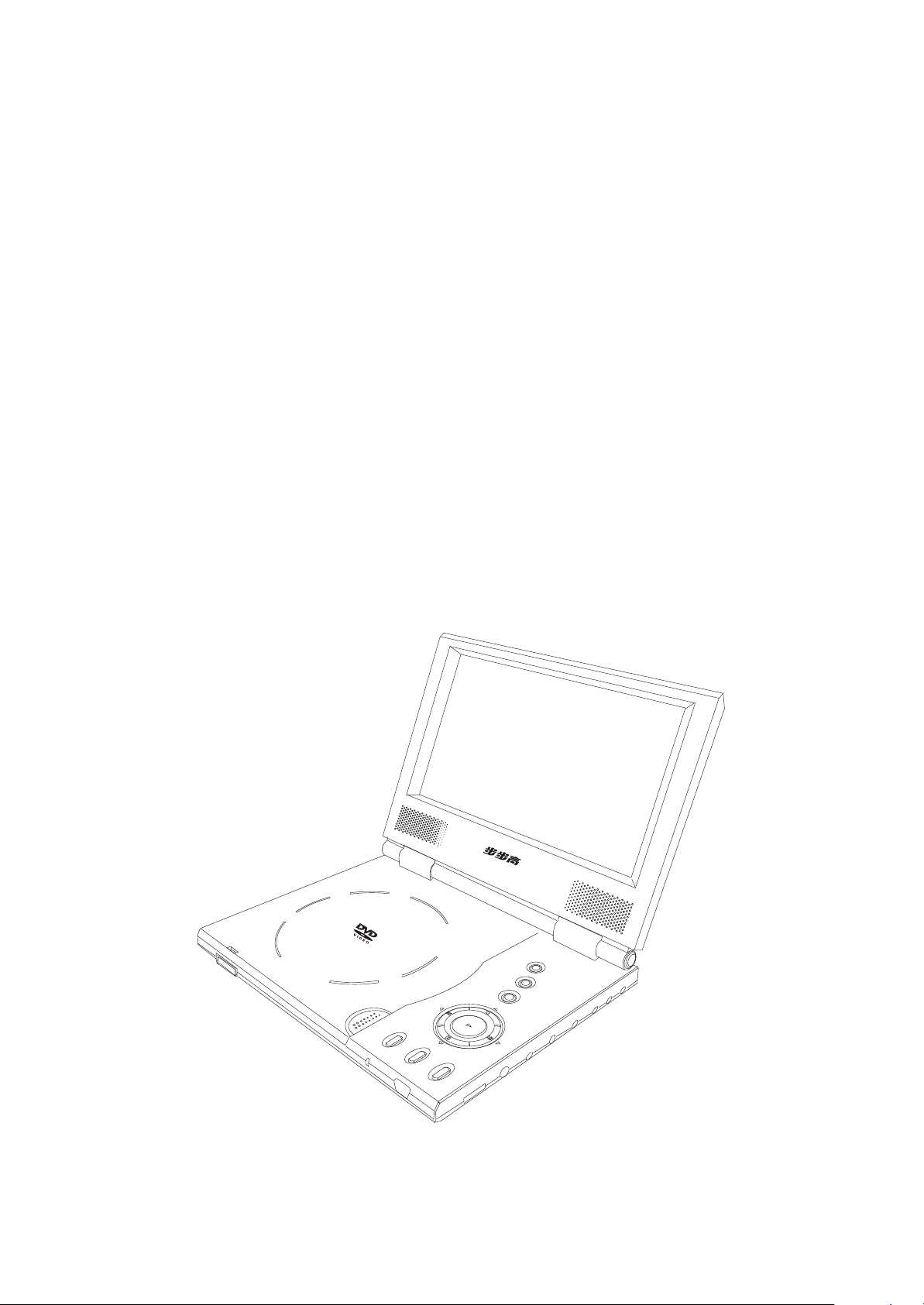
3.Control Button Locations and Explanations
Front Panel Illustration
1
2
DVD-DL333
3
4
5
1
Color TFT LCD
2
Speakers
3
Release slide
4
PREV button / LEFT
direction arrow
5
OPEN/CLOSE button
17
16
15
14
6
7
8
9
10
11
10
11
12
MENU button
PAUSE button / DOWN
13
direction arrow
12
PLAY button / ENTER
button
13
NEXT button / RIGHT
direction arrow
14
6
SET button
7
Power indicator
8
IMAGE button
9
IR sensor
STOP button / UP direction
arrow
15
PANEL/SWITCH button
16
BROWSER button
17
POWER switch
Page 5
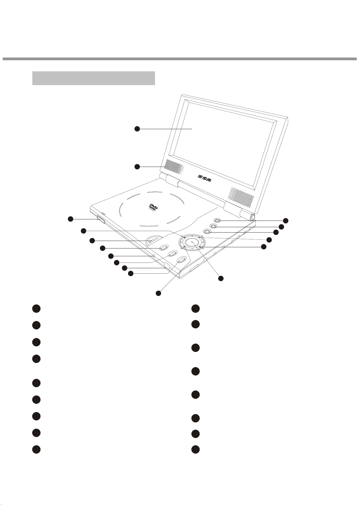
2
3
3
4
5
6
7
8
9
10
11
12
13
14
15
16
17
18
26
SLOW Button
Slow play.
27
MENU Button
Display DVD menu or open/close
PBC.
28
A-B Button
Repeat the select.
29
REPEAT Button
Repeat play.
30
RETURN Button
Back to the previous menu.
2731
PSM Button
Power Spectrum Meter on/off.
2732
IMAGE Buttons
Set video.
33
27
NUMBER Buttons
34
SUBTITLE Button
Change subtitle languages.
35
OSD Button
Display or hide disc information.
35
34
33
32
31
30
29
28
27
26
25
24
23
22
21
20
19
STANDBY Button
Press once to stand by, Press
twice to play.
2
AUDIO Button
Change the audio language or
audio channel.
3
GOTO button
Play from the desired location.
4
ZOOM Button
Zoom in the displayed frame.
5
ANGLE Button
Change camera angles.
6
MUTE button
Press once to mute, twice to unmute.
7
TITLE button
DVD titles.
8
CURSOR Buttons
9
SELECT Button
10
SETUP Button
Function setup.
11
PLAY Button
Normal playback.
12
STOP Button
Stop playback.
13
REV Button
Fast backward play.
14
FWD Button
Fast forward play.
15
KEY Button
Fall tone.
16
KEY Button
Rise tone.
17
P/N Button
Switch the TV system between
PAL, NTSC and AUTO.
18
BROWSER
Switch new user interface.
19
SF Button
Adjusting sound field effects.
20
EQ Button
Adjusting equalization effects.
21
VOLUME-
Decrease volume.
22
VOLUME+
Increase volume.
23
PREV Button
Skip backward.
24
NEXT Button
Skip forward.
25
PAUSE Button
Pause play.
Page 6
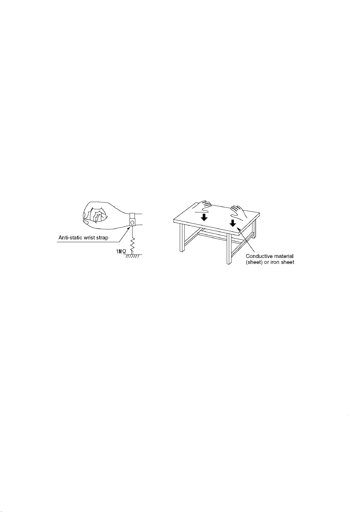
The laser diode in the traverse unit (optical pickup)may brake down due to static electricity of clothes or human
body. Use due caution to electrostatic breakdown when servicing and handling the laser diode.
Some devices such as the DVD player use the optical pickup(laser diode)and the optical pickup will be damaged
by static electricity in the working environment.Proceed servicing works under the working environment where
1. Put a conductive material(sheet)or iron sheet on the area where the optical pickup is placed,and ground the
3. The flexible cable may be cut off if an excessive force is applied to it.Use caution when handling the cable.
4
4.PREVENTION OF STATIC ELECTRICITY DISCHARGE
4.1.Grounding for electrostatic breakdown prevention
grounding works is completed.
4.1.1. Worktable grounding
sheet.
4.1.2.Human body grounding
1 Use the anti-static wrist strap to discharge the static electricity from your body.
safety_3 (1577x409x2 tiff)
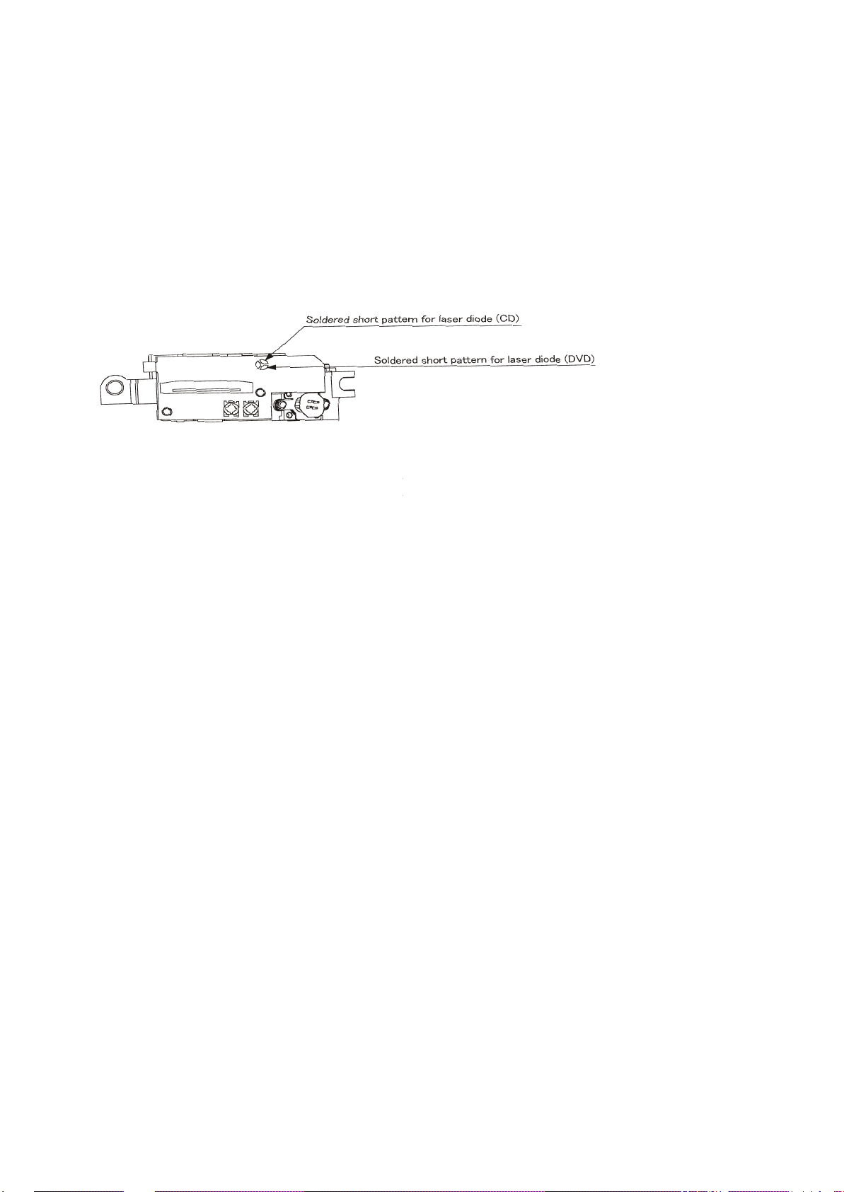
4.1.3.Handling of optical pickup
1. To keep the good quality of the optical pickup maintenance parts during transportation and before
installation, the both ends of the laser diode are short-circuited.After replacing the parts with new ones,
remove the short circuit according to the correct procedure. (See this Technical Guide).
2. Do not use a tester to check the laser diode for the optical pickup .Failure to do so willdamage the laser
diode due to the power supply in the tester.
4.2. Handling precautions for Traverse Unit (Optical Pickup)
1. Do not give a considerable shock to the traverse unit(optical pickup)as it has an extremely high-precise
structure.
2. When replacing the optical pickup, install the flexible cable and cut is short land with a nipper. See the
optical pickup replacement procedure in this Technical Guide. Before replacing the traverse unit, remove
the short pin for preventingstatic electricity and install a new unit.Connect the connector as short times as
possible.
4. The half-fixed resistor for laser power adjustment cannot be adjusted. Do not turn the resistor.
Page 7
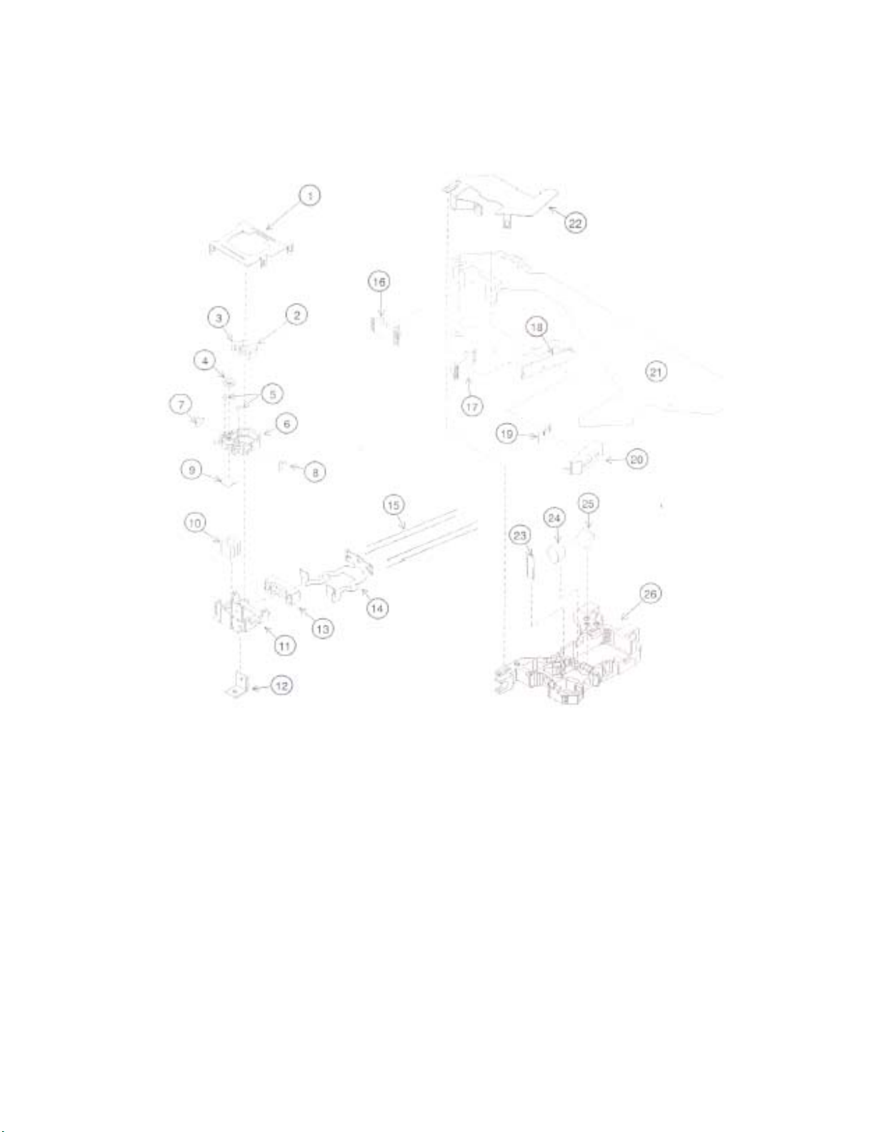
5.1 OPTICAL PICKUP UNIT
5. ASSEMBLING AND DISASSEMBLING THE MECHANISM UNIT
5
Page 8
5.2 MISCELLANEOUS
6
5.2.1 Protection of the LD(Laser diode)
Short the parts of LD circuit pattern by soldering.
5.2.2 Cautions on assembly and adjustment
Make sure that the workbenches,jigs,tips,tips of soldering irons and measuring instruments are
grounded,and that personnel wear wrist straps for ground.
Open the LD short lands quickly with a soldering iron after a circuit is connected.
Keep the power source of the pick-up protected from internal and external sources of electrical
noise.
Refrain from operation and storage in atmospheres containing corrosive gases (such as H2S,SO2,
NO2 and Cl2)or toxic gases or in locations containing substances(especially from the organic silicon,cyan,
formalin and phenol groups)which emit toxic gases.It is particularly important to ensure that none of the
above substances are present inside the unit.Otherwise,the motor may no longer run.
Page 9
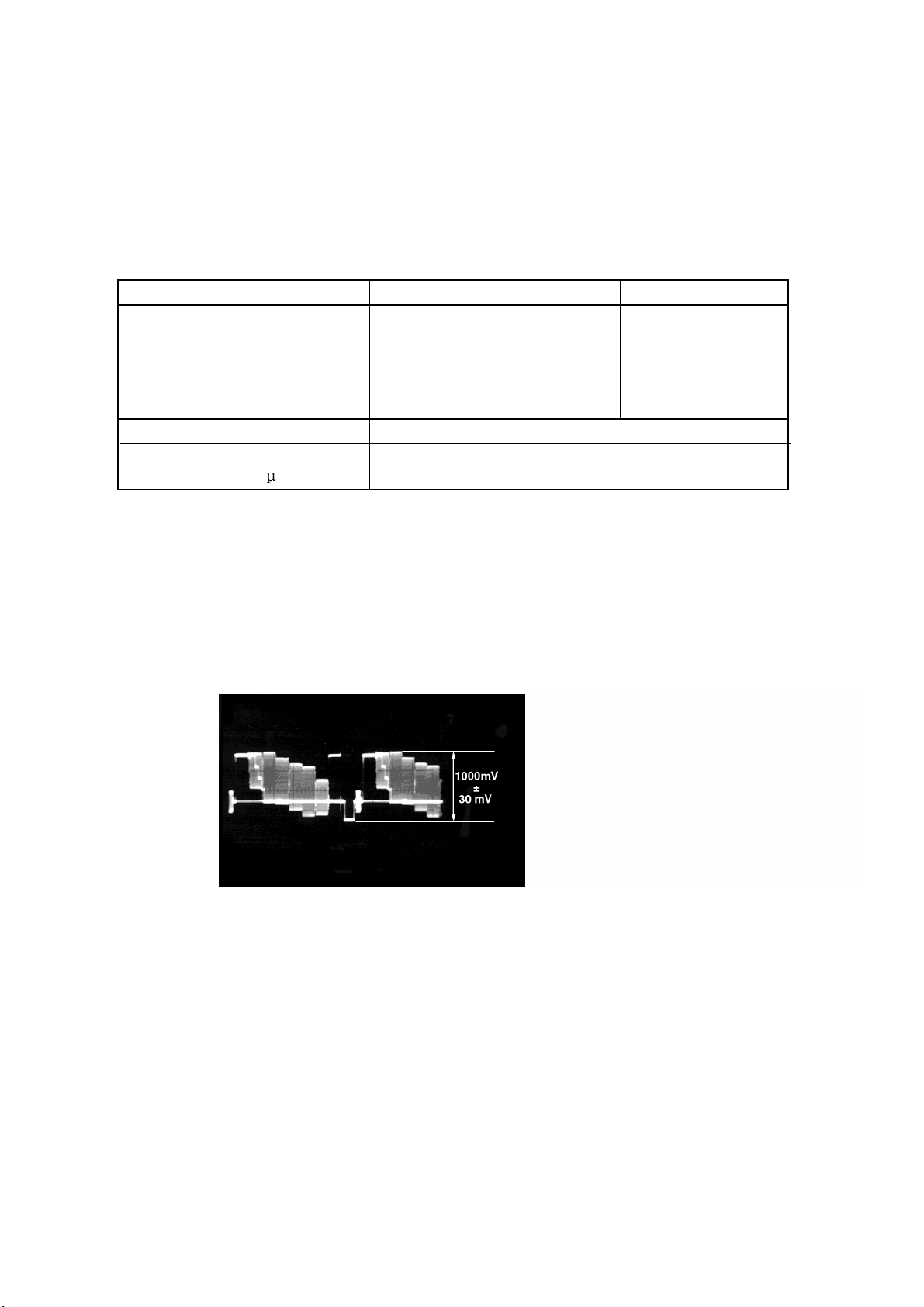
6.1. Video Output (Luminance Signal) Confirmation
6.Electrical Confirmation
7
DO this confirmation after replacing a P.C.B.
Measurement point
Video output terminal
Measuring equipment,tools
200mV/dir,10 sec/dir
Purpose:To maintain video signal output compatibility.
1.Connect the oscilloscope to the video output terminal and terminate at 75 ohms.
2.Confirm that luminance signal(Y+S)level is 1000mVp-p±30mV
PLAY(Title 46):DVDT-S15
PLAY(Title 12):DVDT-S01
Mode Disc
Color bar 75%
Confirmation value
1000mVp-p±30mV
DVDT-S15
or
DVDT-S01
Page 10
Do the confirmation after replacing P.C.B.
Screwdriver,Oscilloscope
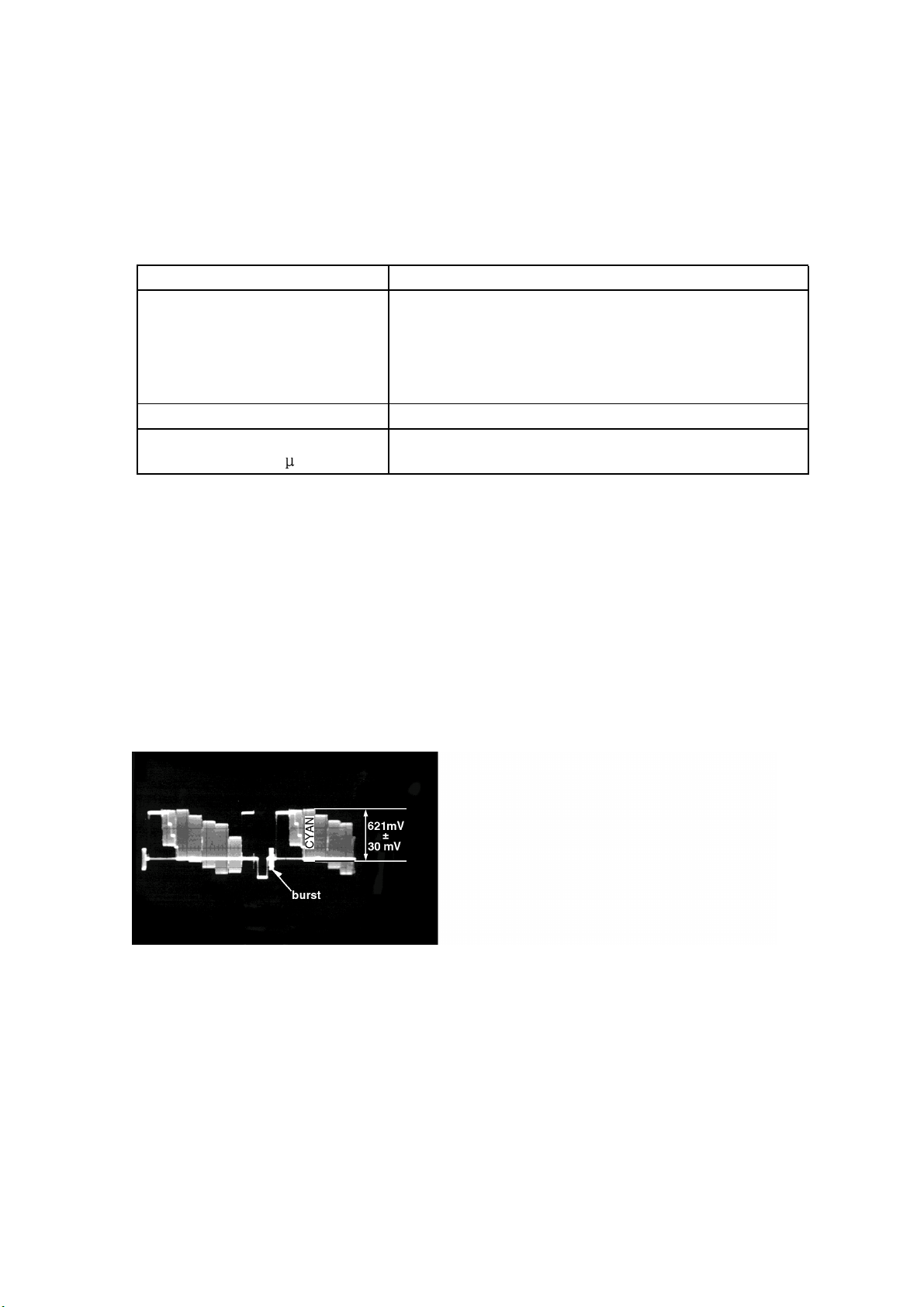
6.2 Video Output(Chrominance Signal) Confirmation
8
Measurement point
Video output terminal
Measuring equipment,tools Confirmation value
200mV/dir,10 sec/dir
Purpose:To maintain video signal output compatibility.
1.Connect the oscilloscope to the video output terminal and terminate at 75 ohme.
2.Confirm that the chrominance signal(C)level is 621 mVp-p±30mV
PLAY(Title 46):DVDT-S15
PLAY(Title 12):DVDT-S01
Mode Disc
Color bar 75%
621mVp-p±30mV
DVDT-S15
or
DVDT-S01
Page 11
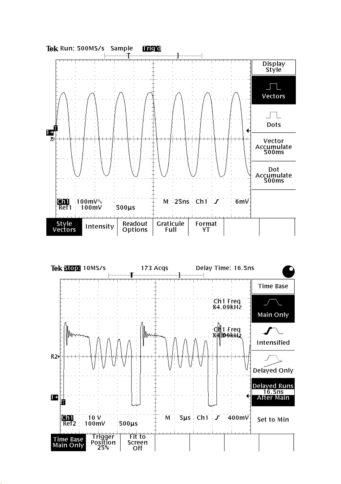
7.MPEG BOARD CHECK WAVEFORM
7.1 27MHz WAVEFORM
7.2 IC5L0380R PIN.2 WAVEFORM DIAGRAM
9
Page 12

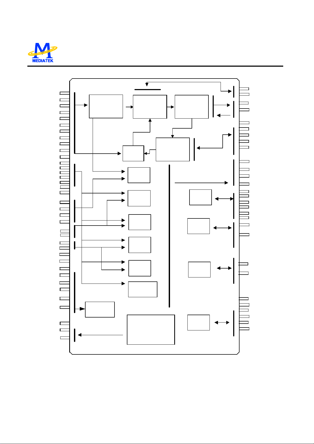
8.1 MT1376
8. IC BLOCK DIAGRAM & DESCRIPTION
10
PRELIMINARY, SUBJ ECT TO CHANGE WITHOUT NOTICE MTK CONFIDENTIAL, NO DISCLOSURE
MT1376
GENERAL DESCRIPTION
MT1376 is a high performance CMOS analog front - end IC for both CD_ROM driver up to 48XS and
DVD-ROM driver up to 16XS. It also supports DVD- RAM read up to 4XS Version 2. It contains servo amplifiers
to generate focusing error, 3-beam tracking error, 1 beam radial push-pull signal, RF level and SBAD for servo
functions. It also includes DPD tracking error signal for DVD_ROM application. For DVD- RAM disks, there are
also Differential Push-Pull (DPP) method for generating tracking signal and Differential Astigmatic Detection
(DAD) for processing focusing signal. Programmable equalizer and AGC circuits are also incorporated in this
chip to optimize read channel performance. In addition, this chip has dual automatic laser power control circuits
for DVD- ROM (DVD-RAM) and CD -ROM seperately and reference voltage generators to reduce external
components. Programmable functions are implemented by the access of internal register through bi-directional
serial port to configure modes selection.
FEATURES
n RF equalizer with programmable
13dB.
n MT1376 supports at least eight different kinds of pick- up heads with versatile input configuration for
both RF input stages and servo signal blocks.
n Versatile on-line AGC.
n 3 beams tracking error signal generator for CD_ROM application.
n One beam differential phase tracking error (DPD) generator for DVD_ROM application.
n Differential push pull tracki ng error (DPP) generator for DVD_RAM application.
n Focusing error signal generator for CD-ROM, DVD-ROM and DVD-RAM (DAD method).
n RF level signal generator.
n Sub-beam added signal for 3 beams CD_ROM.
n One beam push -pull signal generator for central servo application.
n High speed RF envelop detection circuit with bandwidth up to 400KHz for CD-ROM.
n Defect and Blank detection circuits.
from 3MHz to 70 MHz and programmable boost from 3dB to
f
c
n Dual automatic laser power control circuits with programmable level of LD monitor voltage.
n Vref=1.4V voltage and V2ref=2.8V voltage generators.
n V20=2.0V voltage for pick-up head reference.
n Bi-directional serial port to access internal registers.
Page 13
MT1376
11
PRELIMINARY, SUBJ ECT TO CHANGE WITHOUT NOTICE MTK CONFIDENTIAL, NO DISCLOSURE
DVDA
CDA
DVDB
CDB
DVDC
CDC
DVDD
CDD
DVDRFIN
DVDRFIP
DPFN
DPFO
DPDMUTE
CDFOP
CDFON
RFGC
RFGCU
RFGCI
AGC1
AGC2
AGC3
RFSUBO
WOBSO
V20
V2REFO
VREFO
MC
TPI
TNI
MA
MB
MD
OSP
OSN
ATTENUATOR
INPUT MUX
AGC
AGC
SA
SB
SC
SD
IR
VGA
VGA EQ
ENVELOP
ENVELOP
DETECTOR
DETECTOR
DPD
SBAD
TE
PCS
DVD
APC
RFOP
RFON
LRFRP
DEFECT
HRFRP
CRTP
CRTPLP
CSO
LVL
TEO
FEO
REFCOS
HALLCOS
COSPHI
REFSIN
HALLSIN
SINPHI
MDI2
LDO2
RF
LEVEL
FE
CD
APC
MDI1
LDO1
CENTRAL
SERVO
UDGATE
WOBBLE
DET
REF and 2VREF
REF and 2VREF
Voltage Generator
Voltage Generator
SERIAL
PORT
IDGATE
VFO13
SDATA
SLCK
SDEN
MT1376 FUNCTION BLOCKS DIAGRAM
Page 14
12
MT1376
PRELIMINARY, SUBJ ECT TO CHANGE WITHOUT NOTICE MTK CONFIDENTIAL, NO DISCLOSURE
WGND
WOBSO
WVDD
AGNDX
AGNDX
AVDDO
RFOP
RFON
AGNDO
TM1
TM2
TM3
AGNDT
TM4
AVDDT
V2REFO
VREFO
V20
FEO
LVL
CSO
TEO
VDDP
DEFECT
LRFRP
HRFRP
CRTP
CRTPLP
TRLPA
TRLP
HTRC
GNDP
DPFN
DPFO
AGNDX
AGNDX
AGNDX
VDD
VFO13
1
2
3
4
5
6
7
8
9
10
11
12
13
14
15
16
17
18
19
20
21
22
23
24
25
26
27
28
29
30
31
32
33
34
35
36
37
38
RFSUBO
LDO2
LDO1
127
126
125
128
3940414243
MDI1
124
WAVDD
MDI2
123
AGC1
AGC2
AGC3
121
120
119
122
MT1376
DVD-ROM
DVD_RAM
454647
44
48
WAGND
TNI
SGND
118
117
116
With
Read
495051
525453
CDFOP
SVDD
TPI
CDFON
115
114
113
112
111
555657585960616263
SASBMC
IR
AVDDSCSD
110
109
108
MD
AGND
107
106
105
104
103
102
101
100
99
98
97
96
95
94
93
92
91
90
89
88
87
86
85
84
83
82
81
80
79
78
77
76
75
74
73
72
71
70
69
68
67
66
65
64
MB
MA
DVDA
DVDB
DVDC
DVDD
DVDRFIP
DVDRFIN
CDA
CDB
CDC
CDD
OSN
OSP
RFGC
RFGCU
RFGCI
CEQP
CEQN
AGNDX
AGNDX
MON
MOP
SW1
SW2
SWO
SINPHI
REFSIN
HALLSIN
AGNDM
REFCOS
HALLCOS
COSPHI
AVDDM
AGNDX
AVDDF
VCON
AGNDF
IO0
GND
UDGATE
HDGATE
IO4
IO1
IO5
IO7
IO8
IO9
IO6
IO3
IO2
IOB
IOA
MT1376 PIN ASSIGNMENT
SCLK
VDDS
XCK16M
RST
SDEN
GNDS
SDATA
AGNDP
AGNDX
AVDDP
DPDMUTE
Page 15
13
PRELIMINARY, SUBJ ECT TO CHANGE WITHOUT NOTICE MTK CONFIDENTIAL, NO DISCLOSURE
MT1376
MT1376 PIN DESCRIPTIONS
Pin Numbers Symbol Type Description
LQFP128
RF Flag Interface
23 DEFECT Digital Output Flag of bad data output status
RF SIO interface
56 SCLK Digital Input RF serial clock input
58 SDEN Digital Input RF serial data enable
59 SDATA Digital IO RF serial data IO
60 RST Digital input Reset (active high)
55 XCK16M Digital Input 16.9MHz for verification
RF SERVO interface
40 UDGATE Digital Input Con trol signal for DVD-RAM
41 IDGATE Digital Input Control signal for DVD -RAM
38 VFO13 Digital Input DVD -RAM Header signal
RF
100 DVDA Analog input AC coupled DVD RF signal input A
99 DVDB Analog Input AC coupled DVD RF signal input B
98 DVDC Analog Input AC coupled DVD RF signal input C
97 DVDD Analog Input AC coupled DVD RF signal input D
95 DVDRFIN Analog Input AC coupled DVD RF signal input RFIN
96 DVDRFIP Analog Input AC coupled DVD RF signal input RFIP
94 CDA Analog Input AC coupled CD RF signal input A
93 CDB Analog Input AC coupled CD RF signal input B
92 CDC Analog Input AC coupled CD RF signal input C
91 CDD Analog Input AC coupled CD RF signal input D
90 OSN Analog RF Offset cancellation capacitor connecting
89 OSP Analog RF Offset cancellation capacitor connecting
85 CEQP Analog RF Offset cancellation capacitor connecting
84 CEQN Analog RF Offset cancellation capacitor connecting
88 RFGC Analog RF AGC loop capacitor connecting for DVD -ROM
Page 16

14
PRELIMINARY, SUBJ ECT TO CHANGE WITHOUT NOTICE MTK CONFIDENTIAL, NO DISCLOSURE
87 RFGCU Analog RF AGC loop capacitor connecting for DVD -RAM
86 RFGCI Analog RF AGC loop capacitor connecting for DVD -RAM
101 MA Analog Input DC coupled DVD -RAM main-beam RF signal input A
102 MB Analog Input DC coupled DVD-RAM main-beam RF signal input B
103 MC Analog Input DC coupled DVD -RAM main-beam RF signal input C
104 MD Analog Input DC coupled DVD -RAM main-beam RF signal input D
105 SA Analog Input DC coupled DVD-RAM sub-beam RF signal input A
106 SB Analog Input DC coupled DVD -RAM sub-beam RF signal input B
110 SC Analog Input DC coupled DVD -RAM sub-beam RF signal input C
111 SD Analog Input DC coupled DVD -RAM sub-beam RF signal input D
108 IR Analog External current bias resistor (R=20K)
119 AGC1 Analog Wobble AGC loop1 capacitor
121 AGC2 Analog Wobble AGC loop2 capacitor
122 AGC3 Analog Wobble AGC loop3 capacitor
MT1376
127 RFSUBO Analog output Header push-pull RF output signal
1 WOBSO Digital output Wobble signal output
6 RFOP Analog output RF positive output
7 RFON Analog output RF negative output
TRACKING ERROR
32 DPFN Analog DPD amplifier negative input
33 DPFO Analog DPD amplifier output
61 DPDMUTE Digital input DPD mute control input
116 TNI Analog Input 3 beam satellite PD signal negative input
115 TPI Analog Input 3 beam satellite PD signal positive input
21 TEO Analog Output Tracking error output
FOCUSING ERROR & RF LEVEL & CENTRAL SERVO SIGNAL
112 CDFOP Analog Input CD focusing error positive input
113 CDFON Analog Input CD focusing error negative input
18 FEO Analog Output Focusing error output
19 LVL Analog Output RF level output
20 CSO Analog output Central servo signal output
ALPC
Page 17

15
PRELIMINARY, SUBJ ECT TO CHANGE WITHOUT NOTICE MTK CONFIDENTIAL, NO DISCLOSURE
MT1376
124 MDI1
125 LDO1 Analog Ou tput Laser driver output
123 MDI2
126 LDO2 Analog Output Laser driver output
RF RIPPLE
26 CRTP Analog RF top envelop filter capacitor connecting
27 CRTPLP Analog Defect level filter capacitor connecting
25 HRFRP Analog output High frequency RF ripple output or Blank detector’s output
24 LRFRP Analog output Low frequency RF ripple output
POWER
67, 69 AVDD Power Master PLL Filter power
65, 73 AGND GND GND for Master PLL Filter
64 AVDD Power DPD Power
62 AGND GND DPD GND
109 AVDD Power RF path Power
107 AGND GND RF path GND
Analog Input
Analog Input
Laser power monitor input
Laser power monitor input
114 SVDD Power Servo Power
117 SGND GND Servo GND
2,120 WAVDD Power Wobble Power
128,118 WAGND GND Wobble GND
5 AVDDO Power Power for RF output
8 AGNDO GND GND for RF output
14 AVDDT Power Power for Trimming PAD
12 AGNDT GND GND for Trimming PAD
22 VDDP Power Peak Detection Power
31 GNDP GND Peak Detection GND
37,54 VDD Power Serial I/O Power
39,57 GND GND Serial I/O GND
REFERENCE VOLTAGE
16 VREFO Analog output Reference voltage 1.4V
15 V2REFO Analog output Reference voltage 2.8V
17 V20 Analog Output Reference voltage 2.0V
Page 18
16
PRELIMINARY, SUBJ ECT TO CHANGE WITHOUT NOTICE MTK CONFIDENTIAL, NO DISCLOSURE
ALPC TRIMMING
9 TM1 Analog input Trimming pin for ALPC1
10 TM2 Analog input Trimming pin for ALPC1
11 TM3 Analog input Trimming pin for ALPC2
13 TM4 Analog input Trimming pin for ALPC2
HIGH SPEED TRACK COUNTING
29 TRLP Analog Low-pass filter capacitor connecting
28 TRLPA Analog Low-pass filter capacitor connecting
30 HTRC Digital output High speed track counting digital output
PCS
74 HALLSIN Analog input Negative input of amplifier for hall sensor signal
75 REFSIN Analog input Positive input of amplifier for hall sensor signal
76 SINPHI Analog output Amplifier output for hall sensor signal
MT1376
71 HALLCOS Analog input Negative input of amplifier for hall sensor signal
72 REFCOS Analog input Positive input of amplifier for hall sensor signal
70 COSPHI Analog output Amplifier output for hall sensor signal
FOR MONITOR ONLY
81
80
66 VCON Analog output
77 SWO Analog output Output from mux of SW1 & SW2
78 SW2 Analog input External input for servo input select
79 SW1 Analog input External input for servo input select
FOR SERIAL I/O
42
43 IO1
44 IO2
45 IO3
46 IO4
MON Analog output
MOP Analog output
IO0
47 IO5
Page 19

17
PRELIMINARY, SUBJ ECT TO CHANGE WITHOUT NOTICE MTK CONFIDENTIAL, NO DISCLOSURE
48 IO6
49 IO7
50 IO8
51 IO9
52 IOA
53 IOB
MT1376
Page 20

18
8.2 MT1379
Specifications are subject to change without notice
n Super Integration DVD player single chip
§
Servo controller and data channel processing
§
MPEG-1/MPEG-2/JPEG video decoding
§
Dolby AC-3/DTS/DVD-Audio audio decoding
§
Unified track buffer and A/V decoding buffer
§
Video processing for scaling and video quality
enhancement
§
OSD & Sub-picture decoding
§
Built-in clock generator
§
Built-in TV encoder
§
Built-in progressive video output
§
Video input port and audio/SPDIF input port
n Speed Performance on Servo and Decoding
§
DVD-ROM up to 8XS
§
CD-ROM up to 24XS
§
Built-in a frequency programmable clock to µP
and RSPC Decoder to optimize the performance
over power
n Channel Data Processor
§
Provides interface with analog front -end
processor
§
Analog data slicer for small jitter capability
§
Built-in high performance data PLL for channel
data demodulation
§
EFM/EFM+ data demodulation
§
Enhanced channel data frame sync protection &
DVD-ROM sector sync protection
n Servo Control and Spindle Motor Control
§
Programmable frequency error gain and phase
error gain of spindle PLL to control spindle motor
on CLV and CAV mode
§
Provide a varipitch speed control for CLV and CAV
mode
§
Built-in ADCs and DACs for digital servo control
§
Provide 2 general PWM
Progressive Scan DVD Player Combo Chip
§
Tray control can be PWM output or digital output
§
Built-in DSP for digital servo control
n Host Micro controller
§
Built-in 8032 micro controller
§
Built-in internal 373 and 8-bit programmable
MT1379
lower address port
§
1024-bytes on-chip RAM
§
Up to 2M bytes FLASH -programming interface
§
Supports 5/3.3-Volt. FLASH interface
§
Supports power-down mode
§
Supports additional serial port
n DVD-ROM/CD-ROM Decoding Logic
§
Supports CD-ROM Mode 1, CD-ROM XA Mode 2
Form 1, CD-ROM XA Mode 2 Form 2, and CD-DA
formats
§
High-speed ECC logic capable of correcting one
error per each P -codeword or Q-codeword
§
Automatic sector Mode and Form detection
§
Automatic sector Header verification
§
8-bit counter for decode completion check
§
Programmable descrambling and error
correction schemes
§
Automatically repeated error corrections
§
8-bit C2 Pointer counter
§
Decoder Error Notification Interrupt that signals
various decoder errors
§
Provide error correction acceleration
n Buffer Memory Controller
§
Supports 16Mb/32Mb/64Mb/128Mb SDRAM
§
Supports 16-bit/32-bit SDRAM data bus interface
§
Build in a DRAM interface programmable clock to
optimize the DRAM performance
§
Provide the se lf-refresh mode SDRAM
§
Programmable DRAM access cycle and refresh
Page 21

19
PRELIMINARY, SUBJECT TO CHANGE WITHOUT NOTICE MTK CONFIDENTIAL, NO DISCLOSURE
MT1379
cycle timings
§
Block-based sector addressing
§
Programmable buffering counter for buffer status
tracking
§
Maximum DRAM speed is 133MHz
§
Support 5/3.3-Volt. DRAM Interface
n Video Decode
§
Decodes MPEG 1 video and MPEG2 main level,
main profile video (720/480 and 720x576)
§
Maximum input bit -rate of 15Mbits/sec
§
Smooth digest view function with I, P and B
picture decoding
§
Baseline, extended-sequential and progressive
JPEG image decoding
§
RLE and non-RLE BMP image decoding
§
Support CD-G titles
n Video/OSD/SPU/HLI Processor
§
Arbitrary ratio vertical/horizontal scaling of video,
from 0.25X to 256X
§
65535/256/16/4/2-color bitmap format OSD,
§
256/16 color RLC format OSD
§
Automatic scrolling of OSD image
§
Provides 4-color/32x32-pixel hardware cursor
§
Fade-in, Fade out, and Wipe functions as
specified in the DVD-Audio Specification and
other slide show transition effects
§
Progressive scan output
n Audio Processing
§
Decoder format supports:
- Dolby Digital (AC-3) decoding
- DTS decoding
- MLP decoding for DVD-Audio
- MPEG-1 layer 1/layer 2 audio decoding
- MPEG-2 layer1/layer2 2-channel audio decoding
- Dolby Pro Logic decoding
- High Definition Compatible Digital (HDCD)
decoding
§
Up to 6 channel linear PCM output for DVD Audio
/ DVD Video
§
Downmix function
§
Support IEC 60958/61937 output
- PCM / bit stream / mute mode
- Custom IEC latency up to 2 frames
§
Pink noise and white noise generator
§
Karaoke functions
- Microphone echo with adjustable echo level,
echo -depth and delay length
- Microphone tone control with three custom
second-order IIR filter
- Vocal mute/vocal assistant
- Key shift up to +/- 8 keys controlled by 1/2 key
§
Channel equalizer
§
3D surround processing include virtual surround
and speaker separation
§
Power-down control
§
HDCD certified
n TV Encoder
§
Six 54MHz/12bit DA converters
§
Support NTSC, PAL-BDGHI, PAL-N, PAL-M
interlace TV format and 480p, 576p progressive
TV format
§
Automatically turn off unconnected channel(s).
§
Support PC monitor (VGA)
§
Support Macrovision 7.1
n Progressive Output
§
Automatic detect film or video source
§
3:2 pull down source detection
§
Advanced Motion adaptive de-interlace
§
Minimum external memory requirement
n Audio/Video Output
§
Line-in/SPDIF-in for versatile audio processing
§
CCIR601/656 video input port
§
Support picture -in-picture for video decoding and
input source
n Outline
§
216-pin LQFP package
§
3.3/2.5-Volt. Dual operating voltages
Page 22

The 2nd general PWM output
20
PRELIMINARY, SUBJECT TO CHANGE WITHOUT NOTICE MTK CONFIDENTIAL, NO DISCLOSURE
MT1379
P
IN DEFINITIONS
Pin Number Symbol Type Description
1 IREF Analog Input Current reference input. It generates reference current for data
2 PLLVSS Ground Ground pin for data PLL and related analog circuitry
3 LPIOP Analog Output Positive output of the low pass filter
4 LPION Analog Output Negative output of the low pass filter
5 LPFON Analog output Negative output of loop filter amplifier
6 LPFIP Analog Input Positive input of loop filter amplifier
7 LPFIN Analog Input Negative input of loop filter amplifier
8 LPFOP Analog Output Positive output of loop filter amplifier
9 JITFO Analog Output RF jitter meter output
10 JITFN Analog Input Negative input of the operation amplifier for RF jigger meter
11 PLLVDD3 Power 3.3V power pin for data PLL and related analog circuitry
12 FOO Analog Output Focus servo output. PDM output of focus servo compensator
13 TRO Analog Output Tracking servo output. PDM output of tracking servo compensator
14 TROPENPWM Analog Output Tray open output, controlled by microcontroller.
15 PWMOUT1 Analog Output The 1st general PWM output
16 PWMOUT2 Analog Output
17 DVDD2 Power 2.5V power pin for internal fully digital circuitry
18 DMO Analog Output Disk motor control output. PWM output
19 FMO Analog Output Feed motor control. PWM output
20 DVSS Ground Ground pin for internal fully digital circuitry
21 FG Input Motor Hall sensor input
22 HIGHA0 Inout
23 HIGHA1 Inout
24 HIGHA2 Inout
25 HIGHA3 Inout
26 HIGHA4 Inout
27 HIGHA5 Inout
28 DVSS Grou nd Ground pin for internal digital circuitry
PLL.
Connect an external 100K resistor to this pin and PLLVSS.
This is PWM output for TRWMEN27hRW2=1 or is digital output for
TRWMEN27hRW2=0
Microcontroller address 8
2~16MA, SR
PU
Microcontroller address 9
2~16MA, SR
PU
Microcontroller address 10
2~16MA, SR
PU
Microcontroller address 11
2~16MA, SR
PU
Microcontroller address 12
2~16MA, SR
PU
Microcontroller address 13
2~16MA, SR
PU
Page 23

21
PRELIMINARY, SUBJECT TO CHANGE WITHOUT NOTICE MTK CONFIDENTIAL, NO DISCLOSURE
Pin Number Symbol Type Description
29 HIGHA6 Inout
30 HIGHA7 Inout
31 AD7 Inout
32 AD6 Inout
33 AD5 Inout
34 AD4 Inout
35 DVDD3 Power 3.3V power pin for internal digital circuitry
36 AD3 Inout
37 AD2 Inout
38 AD1 Inout
39 AD0 Inout
40 IOA0 Inout
41 IOA1 Inout
42 DVDD2 Power 2.5V power pin for internal digital circuitry
43 IOA2 Inout
44 IOA3 Inout
45 IOA4 Inout
46 IOA5 Inout
47 IOA6 Inout
Microcontroller address 14
2~16MA, SR
PU
Microcontroller address 15
2~16MA, SR
PU
Microcontroller address/data 7
2~16MA, SR
Microcontroller address/data 6
2~16MA, SR
Microcontroller address/data 5
2~16MA, SR
Microcontroller address/data 4
2~16MA, SR
Microcontroller address/data 3
2~16MA, SR
Microcontroller address/data 2
2~16MA, SR
Microcontroller address/data 1
2~16MA, SR
Microcontroller address/data 0
2~16MA, SR
Microcontroller address 0 / IO
2~16MA, SR
PU
Microcontroller address 1 / IO
2~16MA, SR
PU
Microcontroller address 2 / IO
2~16MA, SR
PU
Microcontroller address 3 / IO
2~16MA, SR
PU
Microcontroller address 4 / IO
2~16MA, SR
PU
Microcontroller address 5 / IO
2~16MA, SR
PU
Microcontroller address 6 / IO
2~16MA, SR
PU
MT1379
Page 24

22
PRELIMINARY, SUBJECT TO CHANGE WITHOUT NOTICE MTK CONFIDENTIAL, NO DISCLOSURE
Pin Number Symbol Type Description
48 IOA7 Inout
49 A16 Output
50 A17 Output
51 IOA18 Inout
52 IOA19 Inout
53 IOA20 Inout
54 APLLVSS Ground Ground pin for audio clock circuitry
55 APLLVDD3 Power 3.3V Power pin for audio clock circuitry
56 ALE Inout
57 IOOE# Inout
58 IOWR# Inout
59 IOCS# Inout
60 DVSS Ground Ground pin for internal digital circuitry
61 UP1_2 Inout
62 UP1_3 Inout
63 UP1_4 Inout
64 UP1_5 Inout
65 UP1_6 Inout
66 DVDD3 Power 3.3V power pin for internal digital circuitry
Microcontroller address 7 / IO
2~16MA, SR
PU
Flash address 16
2~16MA, SR
Flash address 17
2~16MA, SR
Flash address 18 / IO
2~16MA, SR
SMT
Flash address 19 / IO
2~16MA, SR
SMT
Flash address 20 / IO
2~16MA, SR
SMT
2~16MA, SR
PU, SMT
2~16MA, SR
SMT
2~16MA, SR
SMT
2~16MA, SR
PU, SMT
4MA, SR
PU, SMT
4MA, SR
PU, SMT
4MA, SR
PU, SMT
4MA, SR
PU, SMT
4MA, SR
PU, SMT
OR Videoin Data PortB 0
Microcontroller address latch enable
Flash output enable, active low / IO
Flash write enable, active low / IO
Flash chip select, active low / IO
Microcontroller port 1-2
Microcontroller port 1-3
Microcontroller port 1-4
Microcontroller port 1-5
Microcontroller port 1-6
MT1379
Page 25

23
PRELIMINARY, SUBJECT TO CHANGE WITHOUT NOTICE MTK CONFIDENTIAL, NO DISCLOSURE
Pin Number Symbol Type Description
67 UP1_7 Inout
68 UP3_0 Inout
69 UP3_1 Inout
70 INT0# Inout
71 IR Input
72 DVDD2 Power 2.5V power pin for internal digital circuitry
73 UP3_4 Inout Microcontroller port 3-4
74 UP3_5 Inout Microcontroller port 3-5
75 UWR# Inout
76 URD# Inout
77 DVSS Ground Ground pin for internal digital circuitry
78 RD7 Inout DRAM data 7
79 RD6 Inout DRAM data 6
80 RD5 Inout DRAM data 5
81 RD4 Inout DRAM data 4
82 DVDD2 Power 2.5V power pin for internal digital circuitry
83 RD3 Inout DRAM data 3
84 RD2 Inout DRAM data 2
85 RD1 Inout DRAM data 1
86 RD0 Inout DRAM data 0
87 RWE# Output
88 CAS# Output
89 RAS# Output
90 RCS# Output
91 BA0 Output
92 DVSS Ground Ground pin for internal digital circuitry
93 RD15 Inout
Microcontroller port 1-7
4MA, SR
PU, SMT
Microcontroller port 3-0
4MA, SR
PU, SMT
Microcontroller port 3-1
4MA, SR
PU, SMT
Microcontroller interrupt 0, active low
2~16MA, SR
PU, SMT
IR control signal input
SMT
Microcontroller write s trobe, active low
2~16MA, SR
PU, SMT
Microcontroller read strobe, active low
2~16MA, SR
PU, SMT
DRAM Write enable, active low
2~16MA, SR
DRAM columnaddress strobe, active low
2~16MA, SR
DRAM row address strobe, active low
2~16MA, SR
DRAM chip select, active low
2~16MA, SR
DRAM bank address 0
2~16MA, SR
DRAM data 15
2~16MA, SR
PU/PD, SMT
MT1379
Page 26

24
PRELIMINARY, SUBJECT TO CHANGE WITHOUT NOTICE MTK CONFIDENTIAL, NO DISCLOSURE
MT1379
Pin Number Symbol Type Description
94 RD14 Inout
DRAM data 14
2~16MA, SR
PU/PD, SMT
95 RD13 Inout
DRAM data 13
2~16MA, SR
PU/PD, SMT
96 RD12 Inout
DRAM data 12
2~16MA, SR
PU/PD, SMT
97 DVDD3 Power 3.3V power pin for internal digital circuitry
98 RD11 Inout
DRAM data 11
2~16MA, SR
PU/PD, SMT
99 RD10 Inout
DRAM data 10
2~16MA, SR
PU/PD, SMT
100 RD9 Inout
DRAM data 9
2~16MA, SR
PU/PD, SMT
101 RD8 Inout
DRAM data 8
2~16MA, SR
PU/PD, SMT
102 DVSS Ground Ground pin for internal digital circuitry
103 CLK Output
DRAM clock
2~16MA, SR
104 CLE Output
DRAM clock enable
2~16MA, SR
105 RA11 Output
DRAM address bit 11 or audio serial data 3 (channel 7/8)
2~16MA, SR
106 RA9 Output
DRAM address 9
2~16MA, SR
107 RA8 Output
DRAM address 8
2~16MA, SR
108 DMVDD3 Power 3.3V Power pin for DRAM clock circuitry
109 DMVSS Ground Ground pin for DRAM clock circuitry
110 RA7 Output
DRAM address 7
2~16MA, SR
111 DVDD3 Power 3.3V power pin for internal digital circuitry
112 RA6 Output
DRAM address 6
2~16MA, SR
113 RA5 Output
DRAM address 5
2~16MA, SR
114 RA4 Output
DRAM address 4
2~16MA, SR
115 DVSS Ground Ground pin for internal digital circuitry
116 DQM1 Output
Mask for DRAM input/output byte 1
2~16MA, SR
Page 27

25
PRELIMINARY, SUBJECT TO CHANGE WITHOUT NOTICE MTK CONFIDENTIAL, NO DISCLOSURE
Pin Number Symbol Type Description
117 DQM0 Output
118 BA1 Output
119 RA10 Output
120 DVDD2 Power 2.5V power pin for internal digital circuitry
121 RA0 Output
122 RA1 Output
123 RA2 Output
124 RA3 Output
125 DVSS Ground Ground pin for internal digital circuitry
126 RD31 Inout
127 RD30 Inout
128 RD29 Inout
129 RD28 Inout
130 DVDD3 Power 3.3V power pin for internal digital circuitry
131 RD27 Inout
132 RD26 Inout
133 RD25 Inout
134 RD24 Inout
135 DVSS Ground Ground pin for internal digital circuitry
136 DQM3 Output
137 DQM2 Output
Mask for DRAM input/output byte 0
2~16MA, SR
DRAM bank address 0
2~16MA, SR
DRAM address10
2~16MA, SR
DRAM address 0
2~16MA, SR
DRAM address 1
2~16MA, SR
DRAM address 2
2~16MA, SR
DRAM address 3
2~16MA, SR
DRAM data 31
2~16MA, SR
PU/PD, SMT
DRAM data 30
2~16MA, SR
PU/PD, SMT
DRAM data 29
2~16MA, SR
PU/PD, SMT
DRAM data 28
2~16MA, SR
PU/PD, SMT
DRAM data 27
2~16MA, SR
PU/PD, SMT
DRAM data 26
2~16MA, SR
PU/PD, SMT
DRAM data 25
2~16MA, SR
PU/PD, SMT
DRAM data 24
2~16MA, SR
PU/PD, SMT
Mask for DRAM input/output byte 3
2~16MA, SR
Mask for DRAM input/output byte 2
2~16MA, SR
MT1379
Page 28

26
PRELIMINARY, SUBJECT TO CHANGE WITHOUT NOTICE MTK CONFIDENTIAL, NO DISCLOSURE
Pin Number Symbol Type Description
138 RD23 Inout
139 RD22 Inout
140 DVDD2 Power 2.5V power pin for internal digital circuitry
141 RD21 Inout
142 RD20 Inout
143 RD19 Inout
144 RD18 Inout
145 DVSS Ground Ground pin for internal digital circuitry
146 RD17 Inout
147 RD16 Inout
148 ABCK Output
149 ALRCK Inout
150 DVDD3 Power 3.3V power pin for internal digital circuitry
151 ACLK Inout
152 MC_DATA Input Microphone serial input
153 SPDIF Output
154 ASDATA0 Inout
155 ASDATA1 Inout
156 ASDATA2 Inout
DRAM data 23 /
2~16MA, SR
PU/PD, SMT
2~16MA, SR
PU/PD, SMT
2~16MA, SR
PU/PD, SMT
2~16MA, SR
PU/PD, SMT
2~16MA, SR
PU/PD, SMT
2~16MA, SR
PU/PD, SMT
2~16MA, SR
PU/PD, SMT
2~16MA, SR
PU/PD, SMT
4MA
4MA,
PD, SMT
4MA
2~16MA,
SR : ON/OFF
4MA
PD SMT
4MA
PD SMT
4MA
PD SMT
Videoin Data PortA 7
DRAM data 22 /
Videoin Data PortA 6
DRAM data 21 /
Videoin Data PortA 5
DRAM data 20 /
Videoin Data PortA 4
DRAM data 19 /
Videoin Data PortA 3
DRAM data 18 /
Videoin Data PortA 2
DRAM data 17 /
Videoin Data PortA 1
DRAM data 16 /
Videoin Data PortA 0
Audio bit clock
(1) Audio left/right channel clock
(2) Trap value in power-on reset :
1 : use external 373 0: use internal 373
Audio DAC master clock (384/256 audio sample frequency)
SPDIF output
(1) Audio serial data 0 (left/right channel)
(2) Trap value in power-on reset :
1 : manufactory test mode 0 : normal operation
(1) Audio serial data 1 (surround left/surround right channel)
(2) Trap value in power-on reset :
1 : manufactory test mode 0 : normal operation
(1) Audio serial data 2 (center/left channel)
(2) Trap value in power-on reset :
1 : manufactory test mode 0 : normal operation
MT1379
Page 29

Analog Y output
27
PRELIMINARY, SUBJECT TO CHANGE WITHOUT NOTICE MTK CONFIDENTIAL, NO DISCLOSURE
Pin Number Symbol Type Description
157 ASDATA3 Inout
158 ASDATA4 Inout
159 DACVDDC Power 3.3V power pin for VIDEO DAC circuitry
160 VREF Analog input Bandgap reference voltage
161 FS Analog output Full scale adjustment
162 YUV0/CIN Output
163 DACVSSC Ground Ground pin for VIDEO DAC circuitry
164 YUV1/C Output
165 DACVDDB Power 3.3V power pin for VIDEO DAC circuitry
166 YUV2/Y Output
167 DACVSSB Ground Ground pin for VIDEO DAC circuitry
168 YUV3/CVBS Output
169 DACVDDA Power 3.3V power pin for VIDEO DAC circuitry
170 YUV4/G Output
171 DACVSSA Ground Ground pin for VIDEO DAC circuitry
172 YUV5/B Output
173 YUV6/R Output
174 ICE
175 BLANK# Inout
176 VSYN Inout
177 YUV7 Inout
178 DVSS Ground Ground pin for internal digital circuitry
179 HSYN Inout
180 SPMCLK Input Audio DAC master clock of SPDIF input /
(1) Audio serial data 3 (surround left/surround right channel)
4MA
PD SMT
4MA
PD SMT
4MA, SR
4MA, SR
4MA, SR
4MA, SR
4MA, SR
4MA, SR
4MA, SR
Input
PD, SMT
4MA, SR
SMT
4MA, SR
SMT
4MA, SR
SMT
4MA, SR
SMT
(2) Trap value in power-on reset :
1 : manufactory test mode 0 : normal operation
OR Videoin Data PortB 1
(1) Audio serial data 4 (center/left channel)
(2) Trap value in power-on reset :
1 : manufactory test mode 0 : normal operation
OR Videoin Data PortB 2
Video data output bit 0 /
Compensation capacitor
Video data output bit 1 /
Analog chroma output
Video data output bit 2 /
Video data output bit 3 /
Analog composite output
Video data output bit 4 /
Green or Y
Video data output bit 5 /
Blue or CB
Video data output bit 6 /
Red or CR
Microcontroller ICE mode enable
Video blank area, active low /
Videoin Field_601
Vertical sync /
Videoin Vsync_601
Video data output bit 7 /
Videoin Data PortB 3
Horizontal sync /
Videoin Hsync_601
Videoin Data PortB 4
MT1379
Page 30

RF serial data output
28
PRELIMINARY, SUBJECT TO CHANGE WITHOUT NOTICE MTK CONFIDENTIAL, NO DISCLOSURE
Pin Number Symbol Type Description
181 SPDATA Input Audio data of SPDIF input /
182 DVDD2 Power 2.5V power pin for internal digital circuitry
183 SPLRCK Input Audio left/right channel clock of SPDIF input /
184 SPBCK Input Audio bit clock of SPDIF input /
185 DVDD3 Power 3.3V power pin for internal digital circuitry
186 XTALO Output Crystal output
187 XTALI Input Crystal input
188 PRST Input
189 DVSS Ground Ground pin for internal digital circuitry
190 VFO13 Output The 1st, 3rd header VFO pulse output
191 IDGATE Output Header detect signal output
192 DVDD3 Power 3.3V power pin for internal digital circuitry
193 UDGATE Output DVD_RAM recording data gate signal output
194 WOBSI Input Wobble signal input
195 SDATA Output
196 SDEN Output RF serial data latch enable
197 SLCK Output RF serial clock output
198 BDO Input Flag of defect data input status
199 ADCVSS Ground Ground pin for ADC circuitry
200 ADIN Analog Input General A/D input
201 RFSUBI Analog Input RF subtraction signal input terminal
202 TEZISLV Analog Input Tracking error zero crossing low pass input
203 TEI Analog Input Tracking error input
204 CSO Analog Input Central servo input
205 FEI Analog Input Focus error input
206 RFLEVEL Analog Input Sub beam add input or RFRP low pass input
207 RFRP_DC A Input RF ripple detect input
208 RFRP_AC Analog Input RF ripple detect input (through AC coupling)
209 HRFZC Analog Input High frequency RF ripple zero crossing
210 PWMVREF A Input A reference voltage input for PWM circuitry. A typical value of 4.0 v
211 PWM2VREF A Input A reference voltage input for PWM circuitry. A typical value of 2.0 v
212 ADCVDD3 Power 3.3V power pin for ADC circuitry
213 RFDTSLVP Analog Output Positive RF data slicer level output
214 RFDTSLVN Analog Output Negative RF data slicer level output
215 RFIN Analog Input Negative input of RF differential signal
216 RFIP Analog Input Positive input of RF differential signal
Videoin Data PortB 5
Videoin Data PortB 6
Videoin Data PortB 7
Power on reset input, active high
PD, SMT
MT1379
Page 31

29
PRELIMINARY, SUBJECT TO CHANGE WITHOUT NOTICE MTK CONFIDENTIAL, NO DISCLOSURE
MT1379
26 Jul, 2002
Page 1 of 2
IREF
PLLVSS
LPIOP
LPION
LPFON
LPFIP
LPFIN
LPFOP
JITFO
JITFN
PLLVDD3
FOO
TRO
TROPENPWM
PWMOUT1
PWMOUT2
DVDD2
DMO
FMO
DVSS
HIGHA0
HIGHA1
HIGHA2
HIGHA3
HIGHA4
HIGHA5
DVSS
HIGHA6
HIGHA7
AD7
AD6
AD5
AD4
DVDD3
AD3
AD2
AD1
AD0
IOA0
IOA1
DVDD2
IOA2
IOA3
IOA4
IOA5
IOA6
IOA7
A16
A17
IOA18
IOA19
IOA20
APLLVSS
RFRP_AC
RFRP_DC
FEI
RFLEVEL
RFDTSLVN
RFDTSLVP
ADCVDD3
212
213
214
59
58
575655
PWMVREF
210
211
60
209
RFIN
RFIP
215
216
1
2
3
4
5
6
7
8
9
10
11
12
13
14
15
16
17
18
19
20
21
FG
22
23
24
25
26
27
28
29
30
31
32
33
34
35
36
37
38
39
40
41
42
43
44
45
46
47
48
49
50
51
52
53
54
HRFZC
PWM2VREF
CSO
TEI
ADIN
RFSUBI
TEZISLV
200
201
202
203
204
205
206
207
208
717069
686766
6564636261
BDO
ADCVSS
198
199
73
72
SLCK
197
74
SDEN
196
SDATA
WOBSI
194
195
777675
UDGATE
193
PRST
VFO13
DVDD3
IDGATE
DVSS
XTALI
XTALO
186
187
188
189
190
191
192
MT1379
(216 pins)
84
838281
807978
DVDD3
SPBCK
184
185
878685
DVDD2
SPLRCK
182
183
89
88
SPDATA
SPMCLK
180
181
HSYN
179
929190
DVSS
178
YUV7
177
VSYN
176
959493
BLANK
175
ICE
174
YUV6/R
YUV5/B
172
173
989796
99
YUV4/G
DACVDDA
DACVSSA
169
170
171
102
101
100
DACVSSB
YUV2/Y
YUV3/CVBS
166
167
168
104
103
105
DACVDDB
DACVSSC
YUV1/C
163
164
165
162
161
160
159
158
157
156
155
154
153
152
151
150
149
148
147
146
145
144
143
142
141
140
139
138
137
136
135
134
133
132
131
130
129
128
127
126
125
124
123
122
121
120
119
118
117
116
115
114
113
112
111
110
109
108
107
106
YUV0/CIN
FS
VREF
DACVDDC
ASDATA4
ASDATA3
ASDATA2
ASDATA1
ASDATA0
SPDIF
MC_DATA
ACLK
DVDD3
ALRCK
ABCK
RD16
RD17
DVSS
RD18
RD19
RD20
RD21
DVDD2
RD22
RD23
DQM2
DQM3
DVSS
RD24
RD25
RD26
RD27
DVDD3
RD28
RD29
RD30
RD31
DVSS
RA3
RA2
RA1
RA0
DVDD2
RA10
BA1
DQM0
DQM1
DVSS
RA4
RA5
RA6
DVDD3
RA7
DMVSS
ALE
IOOE#
APLLVDD3
IOCS#
IOWR#
DVSS
UP1_2
UP1_3
UP1_4
UP1_5
UP1_6
DVDD3
UP1_7
UP3_0
UP3_1
INT0#
IR
UP3_4
DVDD2
UP3_5
UWR#
URD#
DVSS
RD7
RD6
RD5
RD4
RD3
DVDD2
RD2
RD1
RD0
RWE#
CAS#
RAS#
RCS#
BA0
DVSS
RD15
RD14
RD13
RD12
RD11
DVDD3
RD10
RD9
RD8
DVSS
CLK
CKE
RA11
RA9
RA8
DMVDD3
Page 32

30
PRELIMINARY, SUBJECT TO CHANGE WITHOUT NOTICE MTK CONFIDENTIAL, NO DISCLOSURE
MT1379
F
UNCTIONAL BLOCK
IR/
VFD
Servo
IO
Servo
DSP
Playback
Controller
System
Controller
DVD module
Analog
Front end
DRAM
Interface
Spindle
Controller
DPU
Processor
Audio
Channel
Decode
Debug
Port
Audio
Output
CSS/
CPPM
System
Parser
Microphone
Input
Video
Decoder
TV encoder
Video
Output
Servo Controller
The servo control is accomplished through the servo DSP (Servo Digital Signal Processor) and its accessory I/O circuits. This servo
DSP is capable of performing complex operations an d also provides a friendly interface for the system controller. By issuing type
1 and type 2 commands from the system controller, the servo DSP can accomplish various complicated servo control functions,
such as tracking, seeking and MT1336/MT1376 chip register programming. As for the servo I/O circuits, it provides interface
between the input servo signals and the Servo DSP. It has built-in ADCs to digitize the servo control signal and DACs to provide
signals for the actuator and sledge motor. It also has a serial interface to communicate with the MT1336/MT1376 chip.
Analog Front End
The analog front end contains a data slicer circuit and a data PLL circuit. The RF analog signal from MT1336/MT1376 is
quantized by the data slicer to form the EFM/EFM+ bit stream, from which the channel bit clock is extracted by the data PLL.The
EFM/EFM+bit stream and bit clock are then output to DPU for channel bit processing.
DPU
Data path unit (DPU) provides protection on data with lost synchronization patterns and demodulates EFM/EFM+ bit stream into
the channel raw data that will be corrected by the decoder. The synchronization protection makes data after the synchronization
pattern to be extracted even if the synchronization pattern is not found.
Spindle Controller
The sp indle controller is used to control disc spindle motor. It includes a varipitch CLV clock generator, a CLV/CAV controller,
and a PWM generator. The varipitch CLV clock enerator generates a reference colck for the speed of operation. The CLV/CAV
DRAMFlash
Audio DAC
SPDIF
MIC
Page 33

31
PRELIMINARY, SUBJECT TO CHANGE WITHOUT NOTICE MTK CONFIDENTIAL, NO DISCLOSURE
MT1379
controller changes the mode and speed of operation according to servo register setting. The PWM generator generates
pulse-width-modulated signal to drive disc spindle motor driver.
CSS/CPPM
The CSS/CPPM module provides functions necessary for decoding discs conforming to CSS/CPPM specification.
System Parser
The system parser is used to help the system controller to decode DVD/SVCD/VCD bitstream just after the channel decoder
performing error correction. Acting as a DMA master, it moves bitstream data from RSPC buffer to video, audio, or sub-picture
buffer according to system controller request. It also decrypts the scramble data of the CSS/CPPM sectors. Another function of
system parser is providing system controller/DSP a DRAM memory copy controller to enhance system controller/DSP performance.
Video Decoder
The primary function of MT1379 is to support MPEG1 and MPEG2 video decoding. The video decode engine comprises of
variable length decoder (VLD), inverse transformer (IT), motion compensator (MC), and block reconstructor (BR). The video
decode engine decodes the variable length encoded symbols in MPEG bitstream and performs inverse scan, inverse
quantization, mismatch control and inverse discrete cosine transform onto the variable length decoded data. The motion
compensator fetches prediction data from reference picture buffer according to motion vectors and motion prediciton mode for P
and B pictures. Finally, the block reconstructor combines both the results of inverse transformer and motion compensator to derive
the reconstructed image macroblock and write back to picture buffer.
The video decode engine can also support JPEG and BMP file decoding by common image compression hardware kernels.
Video Output
The Video Output unit contains Video Processor, SPU, OSD, Cursor, TV encoder units, it performs
§
§
§
§
§
§
Video Processor
SPU
Reading decoded video from DRAM buffer
Scaling the image
Gamma/Brightness/Hue/Saturation adjustment and edge enhancement
Reading and decoding SPU and OSD data from DRAM buffer
Generating hardware cursor image
Merging the video data, SPU, OSD and cursor
The Video Processor unit controls the transfer of video data stored in the DRAM to an internal or external TV encoder. It uses
FIFOs to buffer outgoing luminance and chrominance data, and performs YUV420 to YUV422 conversion and arbitrary
vertical/horizontal decimation/interpolation, from 1/4x to 256x. With this arbitrary ratio scaling capability, the Video Processor
can perform arbitrary image conversion, such as PAL to NTSC, NTSC to PAL, MPEG1 to MPEG2, Letterbox, Pan-Scan
conversion or zoom in, zoom out. It is also capible of interlace to progressive conversion.
The Video Processor unit performs the following functions:
§
Requests and receives the decoded picture data from the picture buffer in external DRAM for display
§
Resample vertical data to create 4:2:2 sample format
§
Optionally performs vertical/horizontal resampling of both luminance and chrominance data
§
Performs optional Gamma correction, luminance/chrominance adjustment, and edge enhancement
The V ideo Processor unit contains two 2-tap vertical filters for luminance and chrominance . These filters are used to
interpolate and reposition luminance and chrominance line to improve picture quality. These filters are capble of generating
up to eight, unique subline value between two consecutive scan lines. The generation of lines depends on the ratio between
the height of the source image and the target image. In applications where DRAM bandwidth are critical the filters can be
configured as simple line-repeating to reduce the DRAM bandwidth required.
The Video Processor unit integrates two separate horizontal postprocessing filter, a simple 2-tap linear horizontal filter and
an 8-tap programmable filter. These filters are provided for scaling images horizontally along the scan line. These two filters
is capable of generating up to eight, unique subpixel values between two consecutive pixels on a scan line. The generation
of pixels depends on the ratio between the width of the source image and the target image.
Page 34

32
PRELIMINARY, SUBJECT TO CHANGE WITHOUT NOTICE MTK CONFIDENTIAL, NO DISCLOSURE
This is a hardware sub-picture decoder. It decodes the compressed SPU image bitstream and CHG_COLCON commands
according to SPU header information previously decoded by system controller. The SPU module also allows two SPU
objects to be displayed at the same time. SPU image is blended with main video stream.
OSD
The OSD module can operate with 2/4/16/256-color bitmap format (1/2/4/8 bits), and 16/256 color RLC format, all have 16
levels of transparency. In addition, it accepts an special WARP mode, which inserts one programmable RLC code in the
bitmap to reduce the image size stored in DRAM. It also features automatic shadow/outline generation in 2-color mode, 2
Hilight areas, 1 ChangeColor area and 1 OSDVoid area. One OSD area can occupy the full or a partial screen, or multiple
OSDs can occur in a screen at the same time, only if they don't occupy the same horizontal line. The output image is
blended with the video-SPU mixed stream.
Cursor
A hardware cursor generator is integrated in Video Output Unit. The cursor image is a 32x32 4-color bitmap image, each
colors are programmable. Cursor can be enlarged by 2 in both vertical and horizontal directions. Cursor image is multiplexed
with video-SPU-OSD mixed stream.
Audio Interface
Audio interface consists of Audio Output Interface and Microphone Input Interface.
Audio Output Interface
The MT1379 can support up to 8 channel audio outputs. The output formats can be 16, 24, or 32-bit frames. Left alignment,
right alignment, or I2S formats are all supported.
With built-in PLL, MT1379 can provide the audio clock (ACLK) for external audio DAC at 384Fs, where Fs is usually 32KHz,
44.1KHz, 48KHz, 96KHz, or 192KHz. ACLK can also be programmed to be from outside MT1379. When ACLK is input to
MT1379, the frequency could be 128*n Fs, where n is from 1 to 7.
Audio raw (encoded) data or cooked (decoded) data can be output on a single line using S/PDIF interface. The output slew
rate and driving force of this pad are programmable.
Microphone Input Interface
The MT1379 provides a microphone input interface. Two independent microphones’ data could be input to the MT1379.
There are two independent digital volume control for these two input channels. The input data formats can also be left
alignment, right alignment, or I2S formats.
MT1379
System Controller
MT1379 uses an embedded Turbo-8032 as System Controller and provide ICE interface to increase the feasibility of F/W
development. Also, MT1379 includes an build-in internal 373 to latch lower byte address from 8032 Port 0 and provide a
glue-logic free solution. MT1379 supports up to 1M X 16 bits Flash ROM to store 8032 code, H/W related data, User data, etc.
F/W upgrade can be achieved either by debug interface or by disk.
Page 35

33
PRELIMINARY, SUBJECT TO CHANGE WITHOUT NOTICE MTK CONFIDENTIAL, NO DISCLOSURE
MT1379
E
LECTRICAL CHARACTERISTICS
Absolute Maximum Rating
Symbol Parameters Value Unit
VDD3 3.3V Supply voltage -0.3 to 3.6 V
VDD2 2.5V Supply voltage -0.3 to 3.0 V
VDDA Analog Supply voltage -0.3 to 3.6 V
VIN Input Voltage -0.3 to 5.5 V
V
Output Voltage -0.3 to VDD3+0.3 V
OUT
Ta Ambient Temperature 0 to 70 °C
DC Charateristics
Symbol Parameters Min Typ Max Unit
VIH Input voltage high 2.4 - 3.6 V
VIL Input voltage low - - 0.8 V
VOH Output voltage high 3.0 - VDD3 V
VOL Output voltage low - - 0.5 V
IIH High level input current 10 uA
IIL Low level input current -10 uA
PD Power dissapation 1.0 W
P
Power down mode 0.1 W
Down
Page 36

KEY FEATURES
IC BLOCK DIAGRAM & DESCRIPTION
34
8.3 U214 HY29F800
n 5 Volt Read, Program, and Erase
– Minimizes system-level power requirements
n High Performance
– Access times as fast as 55 ns
n Low Power Consumption
– 20 mA typical active read current in byte
mode, 28 mA typical in word mode
– 35 mA typical program/erase current
– 5 µA maximum CMOS standby current
n Compatible with JEDEC Standards
– Package, pinout and command-set
compatible with the single-supply Flash
device standard
– Provides superior inadvertent write
protection
n Sector Erase Architecture
– Boot sector architecture with top and
bottom boot block options available
– One 16 Kbyte, two 8 Kbyte, one 32 Kbyte
and fifteen 64 Kbyte sectors in byte mode
– One 8 Kword, two 4 Kword, one 16 Kword
and fifteen 32 Kword sectors in word mode
– A command can erase any combination of
sectors
– Supports full chip erase
n Erase Suspend/Resume
– Temporarily suspends a sector erase
operation to allow data to be read from, or
programmed into, any sector not being
erased
n Sector Protection
– Any combination of sectors may be
locked to prevent program or erase
operations within those sectors
n Temporary Sector Unprotect
– Allows changes in locked sectors
(requires high voltage on RESET# pin)
n Internal Erase Algorithm
– Automatically erases a sector, any
combination of sectors, or the entire chip
n Internal Programming Algorithm
– Automatically programs and verifies data
at a specified address
n Fast Program and Erase Times
– Byte programming time: 7 µs typical
– Sector erase time: 1.0 sec typical
– Chip erase time: 19 sec typical
n Data# Polling and Toggle Status Bits
– Provide software confirmation of
completion of program or erase
operations
n Ready/Busy# Output (RY/BY#)
– Provides hardware confirmation of
completion of program and erase
operations
n Minimum 100,000 Program/Erase Cycles
n Space Efficient Packaging
– Available in industry-standard 44-pin
PSOP and 48-pin TSOP and reverse
TSOP packages
19
A[18:0]
CE#
OE#
WE#
RESET#
BYTE#
8
DQ[7:0]
7
DQ[14:8]
DQ[15]/A-1
RY/BY#
Page 37

BLOCK DIAGRAM
IC BLOCK DIAGRAM & DESCRIPTION
35
DQ[15:0]
A[18:0], A-1
DQ[15:0]
WE#
CE#
OE#
BYTE#
RESET#
RY/BY#
STATE
CONTROL
COMMAND
REGISTER
PROGRAM
VOLTAGE
GENERATOR
VCC DETECTOR TIMER
ERASE VOLTAGE
GENERATOR AND
SECTOR SWITCHES
A[18:0], A-1
I/O CONTROL
Y-DECODER
X-DECODER
ADDRESS LATCH
I/O BUFFERS
DATA LATCH
Y-GATING
8 Mb FLASH
MEMORY
ARRAY
Page 38

PIN CONFIGURATIONS
IC BLOCK DIAGRAM & DESCRIPTION
36
RY/BY#
A18
A17
A7
A6
A5
A4
A3
A2
A1910
A0
CE#1112
V
SS
OE#1314
DQ0
DQ81516
DQ1
DQ91718
DQ2
DQ101920
DQ3
DQ112122
1
2
3
4
5
6
7
8
PSOP44
44
43
42
41
40
39
38
37
36
35
34
33
32
31
30
29
28
27
26
25
24
23
RESET#
WE#
A8
A9
A10
A11
A12
A13
A14
A15
A16
BYTE#
V
SS
DQ15/A-1
DQ7
DQ14
DQ6
DQ13
DQ5
DQ12
DQ4
V
CC
A15
A14
A13
A12
A11
A10
A9
A8
NC
NC910
WE#
RESET#1112
NC
NC1314
RY/BY#
A181516
A17
A71718
A6
A51920
A4
A32122
A2
A12324
A16
BYTE#
V
SS
DQ15/A-1
DQ7
DQ14
DQ6
DQ13
DQ5
DQ12
DQ4
V
CC
DQ11
DQ3
DQ10
DQ2
DQ9
DQ1
DQ8
DQ0
OE#
V
SS
CE#
A0
10
11
12
13
14
15
16
17
18
19
20
21
22
23
24
A16
1
2
3
4
5
6
7
8
Standard
TSOP48
1
2
3
4
5
6
7
8
9
Reverse
TSOP48
48
47
46
45
44
43
42
41
40
39
38
37
36
35
34
33
32
31
30
29
28
27
26
25
48
47
46
45
44
43
42
41
40
39
38
37
36
35
34
33
32
31
30
29
28
27
26
25
BYTE#
V
SS
DQ15/A-1
DQ7
DQ14
DQ6
DQ13
DQ5
DQ12
DQ4
V
CC
DQ11
DQ3
DQ10
DQ2
DQ9
DQ1
DQ8
DQ0
OE#
V
SS
CE#
A0
A15
A14
A13
A12
A11
A10
A9
A8
NC
NC
WE#
RESET#
NC
NC
RY/BY#
A18
A17
A7
A6
A5
A4
A3
A2
A1
Page 39

HY57V641620HG
37
8.4 HY57V641620HG
4 Banks x 1M x 16Bit Synchronous DRAM
DESCRIPTION
The Hyundai HY57V641620HG is a 67,108,864-bit CMOS Synchronous DRAM, ideally suited for the main memory applications which
require large memory density and high bandwidth. HY57V641620HG is organized as 4banks of 1,048,576x16.
HY57V641620HG is offering fully synchronous operation referenced to a positive edge of the clock. All inputs and outputs are synchronized with the rising edge of the clock input. The data paths are internally pipelined to achieve very high bandwidth. All input and output
voltage levels are compatible with LVTTL.
Programmable options include the length of pipeline (Read latency of 2 or 3), the number of consecutive read or write cycles initiated
by a single control command (Burst length of 1,2,4,8 or Full page), and the burst count sequence(sequential or interleave). A burst of
read or write cycles in progress can be terminated by a burst terminate command or can be interrupted and replaced by a new burst
read or write command on any cycle. (This pipelined design is not restricted by a `2N` rule.)
FEATURES
• Single 3.3±0.3V power supply
• All device pins are compatible with LVTTL interface
• JEDEC standard 400mil 54pin TSOP-II with 0.8mm
of pin pitch
• All inputs and outputs referenced to positive edge of
system clock
• Data mask function by UDQM or LDQM
• Internal four banks operation
Note)
• Auto refresh and self refresh
• 4096 refresh cycles / 64ms
• Programmable Burst Length and Burst Type
- 1, 2, 4, 8 or Full page for Sequential Burst
- 1, 2, 4 or 8 for Interleave Burst
• Programmable CAS Latency ; 2, 3 Clocks
.
Page 40

PIN CONFIGURATION
38
HY57V641620HG
VDD
DQ0
VDDQ
DQ1
DQ2
VSSQ
DQ3
DQ4
VDDQ
DQ5
DQ6
VSSQ
DQ7
DD
V
LDQM
/WE
/CAS
/RAS
/CS
BA0
BA1
A10/AP
A0
A1
A2
A3
DD
V
1
2
3
4
5
6
7
8
9
10
11
12
13
14
15
16
17
18
19
20
21
22
23
24
25
26
27
54pin TSOP II
400mil x 875mil
0.8mm pin pitch
VSS
54
DQ15
53
VSSQ
52
DQ14
51
DQ13
50
VDDQ
49
DQ12
48
DQ11
47
VSSQ
46
DQ10
45
DQ9
44
VDDQ
43
DQ8
42
SS
V
41
NC
40
UDQM
39
CLK
38
CKE
37
NC
36
A11
35
A9
34
A8
33
A7
32
A6
31
A5
30
A4
29
SS
V
28
PIN DESCRIPTION
PIN PIN NAME DESCRIPTION
CLK Clock
CKE Clock Enable
CS Chip Select Enables or disables all inputs except CLK, CKE and DQM
BA0,BA1 Bank Address
A0 ~ A11 Address
Row Address Strobe,
RAS, CAS, WE
LDQM, UDQM Data Input/Output Mask Controls output buffers in read mode and masks input data in write mode
DQ0 ~ DQ15 Data Input/Output Multiplexed data input / output pin
VDD/VSS Power Supply/Ground Power supply for internal circuits and input buffers
VDDQ/VSSQ Data Output Power/Ground Power supply for output buffers
NC No Connection No connection
Column Address Strobe,
Write Enable
The system clock input. All other inputs are registered to the SDRAM on the
rising edge of CLK
Controls internal clock signal and when deactivated, the SDRAM will be one
of the states among power down, suspend or self refresh
Selects bank to be activated during RAS activity
Selects bank to be read/written during CAS activity
Row Address : RA0 ~ RA11, Column Address : CA0 ~ CA7
Auto-precharge flag : A10
RAS, CAS and WE define the operation
Refer function truth table for details
Page 41

FUNCTIONAL BLOCK DIAGRAM
I/O Buffer & Logic
39
1Mbit x 4banks x 16 I/O Synchronous DRAM
HY57V641620HG
Self refresh logic
& timer
CLK
CKE
CS
RAS
CAS
WE
UDQM
LDQM
Row active
State Machine
refresh
Column
Active
Internal Row
counter
Row
Pre
Decoders
Column
Pre
Decoders
1Mx16 Bank 3
X decoders
1Mx16 Bank 2
X decoders
X decoders
1Mx16 Bank 1
1Mx16 Bank 0
X decoders
Memory
Y decoders
Cell
Array
Sense AMP & I/O Gate
DQ0
DQ1
DQ14
DQ15
Bank Select
A0
A1
A11
BA0
BA1
Address buffers
Address
Registers
Mode Registers
Column Add
Counter
Burst
Counter
CAS Latency
Data Out Control
Pipe Line Control
Page 42

6
9.SCHEMATIC & P.C.B WIRING DIAGRAM
FRONT SCHEMATIC DIAGRAM
40
KX023KX124KX21KX32KX43KX54KX65KX6
21
KI0
VD401
1N4148
KI1
KI2
KI3
VD402
1N4148
KI4
VD403
1N4148
SW406
SW1
SW407
SW1
SW408
SW1
SW409
SW1
SW410
SW1
SW401
SW1
SW402
SW1
SW403
SW1
SW404
SW1
SW405
SW1
KEY0
20
KEY1
19
KEY2
18
KEY3
17
KEY4
16
KEY5
15
KEY6
14
KEY7
OSC1
OSC0
VDD
/DREN
REM
SEL
VSS
CSS
11
10
8
13
7
201
455E
201
VSDA
C403
X401
C402
V33
TC401
47uF/16V
HT6222
12
22
KO1
KO0
POWER
V33
VSDA
C401
104
SW411
SW1
POWER
GND
R403
10R
DV33
2
341
XS401
XS04
U401
9
Page 43

FRONT SCHEMATIC DIAGRAM
41
Page 44

FRONT SCHEMATIC DIAGRAM
42
Page 45

U302
MIAN SCHEMATIC DIAGRAM
43
BA5954
XS301
R338 0R
TPI
L301
FBSMT
AVCC
R337 0R
TNI
R336 0R
CDFOP
L303 10uH
XS45
2SB1132-S
V302
4.7R
TC303
T47uF/16V
LDO1
R315
LDO-AVCC
TC308
47uF/16V
R316 20K
FMSO
GND
C334 151
47uF/16V
104
C337
104
TRSO
V1P4
STBY
104
28
PREGND
VINLD23CTK224CTK125VINTK26BIAS27STBY
VINSL+
VINFFC
VINSL-
VINFC
VOSL
CF12CF2
1
3
4
5
6
V1P4
FOSO
R321 20K
C331 151
TC304
C335
C336
22
7
VCC
21
PVCC1
8
9
VCC
PGND
10
VCC
SL-
VOSL-
11
VO2+
SL+
VOFC-
12
VOTK+15VOTK-16VOLD+17VOLD-18PGND19VNFTK20PVCC2
GND
GND
VOFC+
13
R312
1R
R313
1R
T+
T-
29
30
14
R318
1R
R317
1R
GND
SW301
SW2
翻盖 关闭 检测 开关
F-
F+
COVER_SW
R303
DNS
DV33
MCMBMD
MA
DVDD
DVDC
DVDB
DVDA
C315 105
C316 105
C317 105
C318 105
234156891071112141516131718202122192324262728252930323334313637383539404243444145
R340 0R
R341 0R
R342 0R
R343 0R
R344 0R
R345 0R
R346 0R
R347 0R
R348 0R
R349 0R
V1P4
C330
104
C329
104
C340
104
TC301
T47uF/16V
DVDRFIN
C314 105(DNS)DVDRFIP
C350 105
AVCC
CDFOP
C351 105
CDFON
C352 105
ENDM
F-
T-
T+
F+
SL-
SL+
DMSO
FG
L302 10uH
R314
V301
2SB1132-S
LDO2
15R
TC302
T47uF/16V
VCC
LDO-AVCC
R323 DNS
RFVCC
L327
0R
RVCC
R311 DNS
RVCCIN
104
L326 0R
C343
2N3906
AVCC
R309 DNS
LDO-AVCC
DVDRFIN
SASBIOA
104
V303
DVDRFIP
1N4148
L324
FBSMTC328
DV33
L325 0R
V20
VD301
IOB
MDI2
DVDC
DVDD
DVDA
104
DVDB
C341
MDI1
R339 0R
CDFON
SC
SD
CDFOP
CDFON
TPI
TNI
MDI2
MDI1
LDO1
LDO2
15K
R307
104
104
RVCCIN
MD
MC
SA
SB
C312
AGNDO
7
RFON
TM19TM210TM3
8
104
AGNDT
11
12
C301
104
C302
104
10uF/6.3V
C303
104TC306
TC307
10uF/6.3V
C313
TM4
13
V2REFO
AVDDT
14
104
VREFO
15
V2P8
V2017FEO18LVL
16
V1P4
V20
471
CSO
19
FEO
RFL
C311
MT1376E_128
U301
DEFECT
LRFRP
VDDP
TEO
20
21
22
23
CSO
TEO
BDO
C304
391
C305
82pF
C306
333
C307
471(DNS)
CRTPLP
HRFRP
CRTP
24
25
26
RFRP
CRTP
R301
100K(DNS)
TRLPA
TRLP
27
28
153
10pF(DNS)
HTRC30GNDP
29
C308
C309
72
73
REFCOS
31
HTRC
71
COSPHI70HALLCOS
DPFN32DPFO
33
R302 27K(DNS)
69
AGNDX34AGNDX35AGNDX
VDD
36
C310 27pF(DNS)
R324 0R(DNS)
R325 0R(DNS) GND
MA
MB
DD#
CC#
BB#
AA#
102MA101
100
MB
DVDA
DVDB99DVDC98DVDD97DVDRFIP96DVDRFIN95CDA94CDB93CDC92CDD91OSN90OSP89RFFGC88RFGCU87RFGCI86CEOP85CEON84AGNDX83AGNDX82MON81MOP80SW179SW278SW077SINPHI76REFSIN75HALLSIN74AGNDM
103
MC
104
MD
105
SA
106
SB
107
AGND
108
IR
109
AVDD
110
SC
111
SD
112
CDFOP
113
CDFON
114
SVDD
115
TPI
116
TNI
117
SGND
118
WGAND
119
AGC1
120
C319
153
C325
C324
121
122
123
124
125
126
127
128
RVCCIN
WAVDD
AGC2
AGC3
MD12
MD11
LDO1
LDO2
RFSUBO
WGND
47uF/16V
TC305
C320
104
C321
104
C322
104
C323
104
WOBSO
WVDD
1
2
AGNDX3AGNDX4AVDDO
RFOP
5
RVCCIN
RFON
6
RFOP
AGNDF65VCON66AVDDF67AGNDX68AVDDM
AVDDP
AGNDX
AGNDP
DPDMUTE
RST
SDATA
SDEN
GNDS
SCLK
XCK16M
VDDS
HDGATE
UDGATE
GND
VFO13
37
38
C327
104
C326
104
64
63
62
61
PWMOUT2
60
59
58
57
56
55
54
53
IOB
52
IOA
51
IO9
50
IO8
49
IO7
48
IO6
47
IO5
46
IO4
45
IO3
44
IO2
43
IO1
42
IO0
41
40
39
C338
104
C339
104
COVER_SW
RFVCC
URST
SDATA
SDEN
SCLK
IOB
IOA
ENDM
STBY
TROUT
TRIN
ENDM
STBY
R305 10K
R306 10K
Page 46

C241
MIAN SCHEMATIC DIAGRAM
44
47pF
CPU5V
R250 100R
47uF/10V
DRD#
DWR#
DCE#
GND
CTR_R
CTR GLED
IR
VSDA
RXD
TXD
DV33
DWE#
DCAS#
DRAS#
DCS#
BA0
234
1
L203
L201
L202
FBSMT
FBSMT
POWER
VSDA
GND
47pF(DNS)DV33
TC210
C254 103
10RC225
GND
GND2VCC3OUT
R2107 33R
R2108 33R
R2109 33R
C273 47pF
C274
47pF
VD217 1N4148
VD218 1N4148
R288
4.7K
DQ7
DQ6
DQ5
DQ4
DQ3
DQ2
DQ1
DQ0
R229 33R
R230 33R
R231 33R
R232 33R
R233 33R
DQ15
DQ14
DQ13
DQ12
DQ11
DQ10
DQ9
DQ8
XS04
FBSMT
IR
R211
1
XS201
R245
4.7K(DNS)
CPU5V
U203
HS0038B
PRD#
PWR#
PCE#
VSCK
VSTB
SCL
SDA
DCLK
DCKE
DMA11
DMA9
DMA8
4.7R
TC234
47uF/10V
FBSMT(DNS)
225
R213
104
C228
DV33
C280
L206
C222
RA0
RA1
121
122
DMA0
DMA1
A19
DQ10
DQ233DQ3
34
AD10
AD2
RA2
RA3
123
DMA2
14
DQ11
35
AD3
AD0A0A1A2A3A4A5A6A7
DVSS
124
DMA3
1K
VP
Vcc
36
AD1
125
12
37
27pF
X201
27MHz
C223
27pF
R255 0R
XO
AD6
AD5
AD4
AD3
AD2
34
AD237AD138AD039IOA040IOA141DVDD242IOA243IOA344IOA445IOA546IOA647IOA748A1649A1750IOA1851IOA19
DVDD3
RD31
RD30
RD29
RD28
RD27
126
127
128
129
130
131
HOLD_ON/OFF
POWER_ON/OFF
TFT_SW
R242
R224 4.7K
R223 4.7K
R222 4.7K
R299 4.7K
A11
A10
A9
DWR#
A20
10NC13
7
NC
A9
DQ12
DQ1443DQ13
DQ6
DQ540DQ4
39
42
41
38
AD14
AD6
AD13
AD5
AD12
AD4VDAD11
AD7
AD731AD632AD533DVDD335AD336AD4
RD26
132
104
3
A12
DQ7
44
R208 100K
RD25
C2104
A12
DQ15/A-1
XS202
XS04(DNS)
234
1
DV33
RXD
TXD
GND
C224
104
VCC
0R
R212
4.7R
DCLK SDCLK
RDQM0
R234
R235
R246
33R
33R
SDCKEDCKE
DQM0
TC212
10uF/16V
R2158
10K
C281
101
VD DV33
R220
AV33
A16
A17
A18
A19
A20
GND
C226
225
53
52
APLLVSS54IOA20
55
APLLVDD3
56
ALE
57
IOOE#
58
IOWR#
59
IOCS#
60
DVSS
61
UP1_2
62
UP1_3
63
UP1_4
64
UP1_5
65
UP1_6
66
DVDD3
67
UP1_7
68
UP3_0
69
UP3_1
70
INT0#
71
IR
72
DVDD2
73
UP3_4
74
UP3_5
75
UWR#
76
URD#
77
DVSS
78
RD7
79
RD6
80
RD5
81
RD4
82
DVDD2
83
RD3
84
RD2
85
RD1
86
RD0
87
RWE#
88
CAS#
89
RAS#
90
RCS#
91
BA0
92
DVSS
93
RD15
94
RD14
95
RD13
96
RD12
97
DVDD3
98
RD11
99
RD10
100
RD9
101
RD8
102
DVSS
103
CLK
104
CLE
105
RA11
106
RA9
107
RA8
108
DMVDD3
DMVSS
DVDD3
RA7
RA6
RA5
109
110
111
112
113
RDQM1 DQM1
ASPDIF SPDIF#
DMA7
DMA6
R2157
10K
VD201
1N4148
DMA5
DV33
A2
24
8M_FLASH(TSOP)
25
A1
R247
R254
33R
33R
33R
V201
8550
R2159
33R
URST
RA4
114
DMA4
A223A1
CE26A0
DCE#
DVSS
Vss
DQM1
115
27
GND
116
RDQM1
DRD#
DVDD2
DQM0
RA10
BA1
117
118
119
120
RDQM0
BA1
DMA10
R221
4.7K(DNS)
A18
A7A6A5A4A3
A8
18
A619A1717RY/BY15A1816NC
A520A421A322A7
DQ830DQ9
DQ0
DQ1
32
29OE28
31
AD9
AD1
AD8
AD0
R257 0R
XI
A13
A14
A15
30
HIGHA527HIGHA4
DVSS28HIGHA629HIGHA7
MT1379E_216
DQM3
DQM2
RD24
DVSS
133
134
135
136
Vin
GND
Vout
VD
A15
A14
A13
A16
4
A151A142A133A115A106A88A199WE11RESET
BYTE
A16
Vss
45
48
47
46
GNDA0AD7
A17
V1P4
C217
331
C218
331
103(DNS)
C219
C220
153
C221
103
A10
A11
A12
25
26
HIGHA1
HIGHA224HIGHA3
U201
DVDD2
RD23
RD22
137
138
139
R2148R2149
2
U220
R3111H601C
1
330K(DNS)
UPA[20..0]
U214
22
23
RD21
140
141
R214
UPD[15..0]
FGA8A9
RD20
142
RD19
143
+9V
R258 1K
DV33
R207
RD18
FMSO
15K
DVSS
144
NFC
DMSO
R206
10K
DVDD217DMO18FMO19DVSS20FG21HIGHA0
RD17
145
R259 0R
RST#
FBSMT
104
104
104
104
104
104
PWMOUT2
V25
R205
0R
16
PWMOUT1
PWMOUT2
ABCK
RD16
146
147
INT/EXT
POWDET
L204
C245
C246
C247
C248
C249
C250
TROPEN
TRSO
R204
18K
14
15
ALRCK
DVDD3
148
149
150
ABCK
ALRCK
DV33
SD33
TC206
47uF/10V
FOSO
JITFN
102
R203
20K
11
FOO12TRO13TROPENPWM
MC_DATA
ACLK
SPDIF
151
152
ACLK
SDRAM 64M
JITFO
C216
R202
750K
153
ASPDIF
LPFOP
LPFIP
C213
103 C214 103
C215 103
LPION4LPIOP
LPFON5LPFIP6LPFIN7LPFOP8JITFO9JITFN10PLLVDD3
DACVDDC
ASDATA3
ASDATA4
ASDATA0
ASDATA1
ASDATA2
157
158
159
154
155
156
ASDAT0Y0FS
DACV33C
MUTE_DAC
R210 0R
R295 0R
VGND
ASTBASDAT1
AIN-DET
28
VSS54VSS41VSS
VSSQ6VSSQ12VSSQ46VSSQ
49
52
C236
104
R201
C212 103
8.2K
2
3
IREF1PLLVSS
RFDTSLVN
RFDTSLVP
ADCVDD3
PWM2VREF
PWMVREF
HRFZC
RFRP_AC
RFRP_DC
RFLEVEL
TEZISLV
RFSUBI
ADCVSS
SDATA
WOBSI
UDGATE
DVDD3
IDGATE
XTALO
DVDD3
SPBCK
SPLRCK
DVDD2
SPDATA
SPMCLK
BLAANK#
YUV6/R
YUV5/B
DACVSSA
YUV4/G
DACVDDA
YUV3/CVBS
DACVSSB
YUV2/Y
DACVSSB
YUV0/CIN
YUV1/C
DACVSSC
VREF
160FS161
162
VREF
R237 390R
DQM0
DQM1
39NC36NC40
VCCQ3VCCQ9VCCQ43VCCQ
LPION
RFIP
RFIN
CSO
ADIN
BDO
SLCK
SDEN
VFO13
DVSS
PRST
XTALI
HSYN
DVSS
YUV7
VSYN
ICE
LPIOP
FEI
TEI
DWE#
104
DRAS#
DCAS#
27
R252
4.7R
C272
C240
104
TC204
47uF/10V
216
215
214
213
212
211
210
209
208
207
206
205
204
203
202
201
200
199
198
197
196
195
194
193
192
191
190
189
188
187
186
185
184
183
182
181
180
179
178
177
176
175
174
173
172
171
170
169
168
167
166
165
164
163
DCS#
VCC1VCC14VCC
SD33
AV33
104
R251
104
104
4.7R
104
104
104
GND
RFRPC
CTR_POWERDOWN
CTR_SDRAM
1K(DNS)
VGND
C237
104
ASDAT0 SDATA0
R294 33R
BA0
#BA1
SDCLK
SDCKE
20
21
BA1/A12
CLK38CKE37/CS19/RAS18/CAS17/WE16DQML15DQMH
53
DQ12
DQ13
DQ14
DQ15
104
C227
104
C253
104
C208
104
C209
104
C210
104
C211
RFON RFIN
DV33
C238 102
C239 102RFOP
RFIP
RFZC
RFL
FEO
CSO
TEO
ADIN
BDO
SCLK
SDEN
SDATA
URST
XI
XO
CTR_TFT
CTR_AUDIO
VGND
R236
VGND
DACV33A
Y3
VGND
Y2
DACV33B
Y1
VGND
ACLK SACLK
ABCK SBCLK
ALRCK SLRCK
R291 33R
R292 33R
R293 33R
33R
33R
DMA8
DMA9
DMA10
MA11
DQ1045DQ1147DQ1248DQ1350DQ1451DQ15
44
DQ8
DQ9
DQ10
DQ11
C207
C202
C203
C204
C205
C206
R297
R298
C233
102
DMA7
DQ7
V25
GND
10uF/10V
TC201
C234
104
RFRP
R216 18K
1K
V25
FBSMT
47uF/10V
FBSMT
DMA11
BA1
DMA4
DMA5
DMA6
DQ4
DQ5
DQ6
4
VSS
5
SDA
V2P8
R215
L330
104
TC215
L329
DMA3
DQ3
2
3
WP/RST_
RST/WP
SCL6SDA
7
SCL
HTRC
RFRPC
R219 0R
104
104
DV33
10uF/10V
C232
104
DMA1
DMA2
DQ1
DQ2
DC/NC1RST_/NC
VCC
8
C201
104
1K
1K
R218 0R(DNS)
C230
C231
TC202
C279
104
DMA0
U211
A023A124A225A326A429A530A631A732A833A934A10/AP22A1135BA0/A13
DQ02DQ14DQ25DQ37DQ48DQ510DQ611DQ713DQ842DQ9
DQ0
AT24C02/X4050
U202
DV33
R227
R228
R217 100K
V1P4
DACV33C
10uF/10V
TC214
L331
FBSMT
C235
Page 47

AGND
MIAN SCHEMATIC DIAGRAM
45
10uF/16V(DNS)
L218
FB
VGND
GND AGND
104
104
104
1.0
0R(DNS)
TC207
47uF/16V
TC244
R2138
470R(DNS)
A5V
VCC
FBSMT
C2151
C2150
C2152
R261
+9V CPU5V
U212
78L05
3
IN
2
GND
1
OUT
C283
10uF/16V
+9V VCC
C284
104
RVCC
C285
104
VCC V25
3
C282
104
1
AVCC
L219
VCC
IN
ADJ
OUT
R2137
150R(DNS)
R2115
75R
C259
270pF
C260
330pF
VGND
VGND
AMS1084(DNS)
2
2
AGND
R239
150R
Y3
1.8uH
V213
3906
20pF(DNS)
C263
U206
LED201
R-G LED
MUTE_DAC
8050
AGND
DNS
L207
CVBS
FBSMT
421
3
1 3
VD211
1N4148
R253
1K
V203
R238
AGND
VGND
VGND
150R
TC231
220uF/16V
L212
CVS
JK207
VIDEO-OUT
330R
8550
47uF/16V
47pF
47pF
R270
10uF/10V
R226
RED
V210
TC235
39R
C258
C261
TC209
10uF/10V
330RTC245
47uF/10V
104
104
47uF/6.3V
330R
1K
8550
R241
1K
VD202
1N4148
8550
R2114
1.8uH
3906
VCC
104
27pF
R244
TC230
C271
C269
TC211
A5V
R2101
MUTEC V202
R2106
V205
1N4148
+9V
Y1
L208
V209
C278
C277
6
1
200R
10K
R2139
1K
R2105
1K
1K
8550
MUTE-1
VD203
220uF/16V
33R
V25
8050
+9V
R240
V204
TC217
DV33
23415
ADJ
R243
ASTB
R2127
V206
VCC
R268
150R
SPDIF#
R260
OPTICAL
3
AMS1084
IN
OUT
2
VD213
HER105
C270
104
TC213
47uF/10V
R2126
DNS
104(DNS)
C252
12C508A
GP25GP16GP0
STB
TO TFT-LCD
XS08
VGND
VCC
VGND
20pF(DNS)
JK201
VCC
U208
FBSMT
POWER
1
GP52GP43GP34vdd
GND
7
8
GND
IR
STBT
VD208
1N4148
C#Y#VGND
L227
L214
FBSMT
FBSMT
7
39R
47pF
47pF
20pF(DNS)
C264
C265
L205
AV33
R2104
10K
10K
U215
10K
SW201
SW2
LSOUT+
LSOUT-
L226
L228
FBSMT
FBSMT
R2113
C257
C262
FBSMT
S-Video
DV33
R2103
R2102
RSOUT-
L225
FBSMT
1.8uH
3906
L211
C
FBSMT601
DGND
STBTA
NFC
RSOUT+
L224
L223
FBSMT
FBSMT
2341568
XS205
Y2
L209
V211
220uF/16V
L210
FBSMT
Y
421
3
JK204
L213
R2125 27K
DGND DGND
CPU5V
R209
10K
AGND
104
10K
101
R2124
10K
100uF/16V
150R
TC250
C2127
Vin
DNS
104
104
47uF/16V
R2123
C295
ZA3020
GND
VD210
1N5819
TC218
47uF/16V
DGND
AGND
CPU5V
TC216
R269
RSOUT+
AGND
C#
1
3
TC227
C292
C293
TC219
C294 223
SYNC
STB
5
Sync8EN7Comp6FB
Vsw
Vin
BS
1
2
3
4
L221
22uH TC205
C297
104
100uF/16V
VCC
JK208
POWER SUPPLY
+9V
DGND
R275
100K
VCC
Y#
11
10
2
JK206
U216
C296 103
DGND
L222
10uH
104
L232
FBSMT601
11
12
13
14
15
16
17
18
19
20
AGND
+9V
L220
10uH
TC248
47uF/16V
C2125
104
TC249
47uF/16V
+5VA
C298
1
78L05
105
R2143
20K
C286 DNS
R2142
DNS
C2128
334
GND
GND
+INB
BYPASS
-INB
-OUTB
VDD
+OUTB
GND
SHUTDWN
HP-IN
R2144
100K
R277
1K
JK203
HP
R267 33K
L233 10uH
+5V
100mA
+9V
GND
IN3GND2OUT
50K*2
C2102
DGND DGNDDGND
DGND
10uF/16V
104
100uF/16V
10uF/16V
U213
ROUT
GND
GND
+INA
GND
-INA
-OUTA
VDD
+OUTA
GND
LM4863MTE
TC222
100uF/16V
3
104
47uF/16V
10K
10K
VD212
1N5819
VD220 1N4148 -10V
TC236
C251
L229 10uH
TC239
3mA
TC220
LOUT
VR201
C2103 105
C287 DNS
10
9
8
7
6
5
4
3
2
1
U209
R2145
100K
1K
421
C291
TC224
R265
C2121
101
R266
TRANS333
6
DGND
VD219
10V/1W
+5VA
GND
+5V
7
R2140
20K
R2141
DNS
AGND
VDD
R276
4
BS1Vin2Vsw3GND
Comp
Sync
6FB5
STBTA
C2120
223
22uH
4
7109
8
47uF/16V
TC246
C2124
104
TC247
47uF/16V
+15V
+7.5V
GND
R274 100K
LSOUT-RSOUTLSOUT+
TC221 100uF/16V
VGND
L215
10uH
U217 ZA3020
8EN7
R225 0R(DNS)
SYNC
2
VD216 1N4148 +7.5V
GND
L230 10uH
15mA
-10V
GND
2341568
AGND
AGND
1K
8050
C2119
103
T201
33uF/25V
104
XS206
XS08
STB
R2146
V212
104
TC240
C2123
4.7K
C243
104
C229
10uF/16V
2
LM7805
U221
10K
1N4148
GND
+15V
1mA
R2122
3.9K
IN
GND
OUT
C268
104
TC223
47uF/16V
AGND
R2147
VDD
TC237
VD215
AGND
1
3
AGND
+8V
C275
104
C276
104
C244
104
R279 33R(DNS)
R280 0R R283 DNS
R281 0R
R282 0R
8
FILT+
10uF/16V
6
7
TC241
CH-R
R2120
ROUT
L217
Rt
10uF/16V
Ain
104
TC233
104
10uF/16V
TC226
R2135
10K
R2132
10K
R2134
4.7K
+8V
102
AGND
TC229
9
C255
C256
TC232
ARIN
33K
C2114 101
R21191KR2118
V208
2SC1815-Y
R2112
100K
AGND
C2101
ALIN
AIN-DET
ARIN
TC228 10uF/16V
JK202
AGND
VD214 DNS
TC238
DNS
C2122
DNS
-5V
10uF/16V
R249
DNS
C2116
102
C2115
152
5
4 8
U219B
4580
10uF/16V
R2121
+8V
330R
+9V
FBSMT
VDD
R263
1K
R264
1K
AGND
SDA
R287
AGND
R2133 20K
SCL
R278 33R(DNS)
REF-GND
11VQ10
100K
0R(DNS)
47uF/16V
SACLK
AOUTB
12
RRLLMUTECRST#
1K
2SC1815-Y
R262
+9V +8V
R256
3
IN
2
GND
1
OUT
TC208
SDATA0
SBCLK
SLRCK
R284 DNS
R285 DNS
U207 CS4340/1
RST1SDA2SCLK3LRCK4MCLK5DIF16DIF07DEM0
MUTEC16AOUTA
AGND
15VA14
13
C288
104
R296
0R
CPU5V
R248
DNS
R2136
10K
C2113
102
R2131
10K
C2112
152
R2130
4.7K
3
2
4 8
U219A
4580
1
TC242
10uF/16V
MUTE-1
CH-L
R2117
330R
V207
LOUT
R2111
100K
L216
FBSMT
C299
102
Lt
VCC
6
78L08
TC203
10uF/16V
TC225
10uF/16V
C2111 101
+8V
23415
33K
U210
ALIN
A-out
A5V
R286
R2129 20K
JK201
Page 48

MIAN SCHEMATIC DIAGRAM
46
Page 49

MIAN SCHEMATIC DIAGRAM
47
Page 50

CC52
LCD DRIVE BOARD
48
104
VCON
VCOP
TIN
TINT
2cy3
5
6
7
8
VCC1
VCOM
VCOM
5
8
6
V+
O/P B7-I/P B
+I/P B
O/P A1-I/P A2+I/P A3GND
UC04
20K
RC38
47K
VCC1
RC33
22K
RC29
33K
RC25
10K
RC21
33K
NJM3414AM
4
RC43
RC42
10K
RC39
5.1K
BRT
CNT
QC01
2SC2412K
RC34
5.1K
COL
TIN
RC22
5.1K
SBB
-10V
RC46
20K
RC44
10K
VCC1
RC40
5.1K
RC35
5.1K
RC32
RC28
RC23
5.1K
TCC05
10uF/16V
RC45
10K
COMO
RC41
33K
CC10
103
CC09
103
RC37
27K
RC36
20K
39K
CC08
103
15K
VCC1
CC07
103
RC24
22K
CC06
103
4
c
cx
by1bx
INH
VSS
VEE
UC05
16
VCC1
VCO
22uH
LC03
CVBS
RC57
1K
RC56
470K
C9B10A11ax12ay13a14b15vdd
BU4053BCF
GO
RC78
NPC
NPC
NPC
Vid
22uH
CC11 33pF
CVBS
LC04
CC13 56pF
CC12 56pF
CVBS
CVBS
CVBS
CC36
+7.5V
GM2
GM0
RGB
BRT
SBB
SBR
FRP
FRP
/HSY
CSYN
104
TCC06
47uF/16V
BO
100R
CC35
1uF/50V
RC79
23
24
UC01
VCC2
B OUT
B DC DET
25
GM2
26
GM0
27
28
29
30
31
32
33
34
35
36
CC16
821
BRIGHT
SBB
SBR
COM FRP
FRP
SY NC IN
RGB AMP ADJ
SY NC OUT
SY NC SEP
COM ADJ
COM OUT38SW39B IN40G IN41R IN42VCC143F ADJ44CLAMP45AGC FILTER46AGC OUT
37
COMA
COMO
100R
CC34
1uF/50V
CC33
1uF/50V
RO
RC77
100R
VCO
APC
19
14
15
16
18
20
21
22
GND117GND2
R OUT
G OUT
G DC DET
VCO IN
VCO OUT
R DC DET
APC FILTER
IR 3Y29B
47
GNDD
GND
RC80
0R
RC81
0R
GNDD GND
VCC1
note:
1. the value of TC29,TC30 depand on and u6.
RC76
5.6K
RC75
8.2K
TCC07
474
APC
CC32
103
CC31
OPEN
CC30
15pF
YC01
RC74
3K
RC73
1.5K
TINT
13
TINT
PICTURE
48
PIC
3.58MHz
VCON
CC29
12pF
IR3Y29B
CHROMA OUT
12
ACC FILTER
11
B-Y
10
R-Y
9
KILLER FILTER
8
BURST OUT
7
COLOR
6
C IN
5
IDENT FILTER
4
VIDEO IN
3
CONTRAST
2
T RAP
1
VCOP
YC02
4.43MHz
COL
CNT
TCC03
10uF/16V
RC65
0R
RC141
330R
4. For STD R/G/B input :set SW (pin4 of JP1)=H
2. TCC02and TCC04 with high ripple current
capability
and low ESR are the best choice
3. LC02 should be adjustable for PAL system.
For S-video (Y/C) input:
R60,R65,R66: OPEN
R64,R67: 000
VCC1
RC72
330R
QC03
3906
RC71
RC70
5.6K
CC20
681
RC66
10M
VCC1
1.5K
RC69
5.6K
CC27
103
CC28
82pF
CC26
103
RC68
1M
CC25
104
CC24
473
LC02
23uH
CC23
103
CC22
56pF
RC02
39R
CC21 10 4CVBS
RC67
39R
RC17
33K
RC18
RC13
33K
RC14
RC09
39K
RC05
22K
RC06
RC01
47K
RC19
5.1K
SBR
RC15
5.1K
RGB
GM0
RC07
5.1K
5.1K
GM2
PIC
RC63
+5V VCCU
ROU
AGNDA
LOU
AGNDA
2341567
FROM MPEG
VCC1
TCC04
330uF/16V
0R
LC01
150uH CR32
CC19
104
CVBS
GND
LOU
AGNDA
ROU
AGNDA
2
1
2
XS07
1
XSC04
XS02
XSC05
XS02
RC20
22K
5.1K
CC05
103
RC16
20K
5.1K
CC04
103
RC12
10K
CC03
103
RC08
20K
CC02
103
RC04
56K
CC01
103
RC55
560R
CC15
1uF/50V
RC52
75R
CVBS
RC47
15K
VCC1
COMA
RC58
10K
RC59
18K±1%
CC17 68 2
TCC01
VCC1
RC50
12K
CC14
103
OPEN
RC60
0R
RC61
OPEN
BRT
RC64
0R
Vid
TCC02
330uF/16V
CC18
104
RC62
330K
COL
F/N
XSC01
Page 51

XSC03
LCD DRIVE BOARD
49
123456789
GND
DVDD
VGL
These signals are outputs
D(1:26)
CPH1
CPH2
CPH3
RC125
100R
RC126
100R
RC124
100R
CK3A
RC127
CK2A
CK1A
CKV
RC130
F/N
to panel!
STHL
STHR
CLK
560R
RC128
560R
RC129
NOTE
RC131
NOTE
RC132
VGH
STVL
RC123
100R
560R
NOTE
CC44
2.2uF/50V
1011121314151617181920212223242526
STVR
STVL
CLK
U/D
OEV
L/R
MOD
OEH
VCOM1
VCOM1
OPEN
100R
VCCU
UC02
13
14
15
16
17
18
19
20
21
22
23
24
GNDD
MOD
RC1200RRC121
9
11
12
VO210VO1
VCC
STHL
STHR
PD_OUT
V_CK
CK1A
CK2A
CK3A
ZX1
ZX2
ZX3
GND
VCC
F_OUT25F_IN26VSY_OUT27HSYW28GR_IN29V_IN30UD_OUT31ZTC32AUXS33HSY_OUT34CSYNC35GND
STVR
RC122
VCCU
STHL
STHR
CPH3
CPH2
CPH1
ROUT
DVDD
GND
OEV
OEH
GNDD
RC118
560R
RC117
RC119
OPEN
2
4
5
6
7
8
GND
RES_C
D_MOD
HZ_OUT
FDV_OUT
HOE_OUT3VOE_OUT
MOD_OUT
UPS017
26PIN
GOUT
BOUT
DVDD
GND
D1:GND
D2:VCC (+5V)
D3:VGL
D4:VGH
D5:STVR
D6:STVL
D7:CLK
D8:U/D
D9:OEV
D10:VCOM
D11:VCOM
D12:L/R
D13:MOD
D14:OEH
D15:STHL
D16:STHR
D17:CPH3
D18:CPH2
D19:CPH1
D20:DVDD
D21:DVSS
D22:VA
D23:VB
D24:VC
D25:AVDD
D26:AVSS
L/R
U/D
560R
560R
RC116
RC115
560R
CC51
PORT1
PORT2
RC114
100R
RC113
100R
1
VCCU
UPS017
NPFRP
VCC
48
CP_IN
47
CP_OUT
46
NP_SW
45
PFRP_OUT
44
NPC
43
TC
42
CSYN_OUT
41
LR_A
40
L_R
39
PD_SW
38
UDC
37
36
RC107 1K
391
750R
RC112
RC1091KRC110
NPC
RC03 1K
GNDD
GNDD
1K
TCC09
10uF/16V
RC108 100R
RC10 1K
FRP
VGH
VGL
RC136
10K
RC135
100K
560R
100R
TCC11
10uF/16V
RC133
RC134
CC50
104
+15V
-10V
VCOM
RC139
30K
RC138
56K
VCOM1
CC49
104
VCC1
RC94
100R
CC48
TCC08
RC92
1M
LC05
RC90
2.4K
GNDD
CC39
222
RC93
100R
CC43
1.5uH
22pF
GNDD
1 3
2
RPC01
DC01
MA335
CC41
CC40
104
OPEN
RC89
10K
CC38
CC37
561
RC84
RC83
1M
RC82
24K
RC91
10K
GNDD
104
O4V
-3G2+
UC03
82K
-10V
2.4K
CC42
5
NJM2107
1
RC86
GNDD
RC85
VCC1
104
GNDD
GNDD
68K
RC88
4.7K
47K
RC87
4.7K
VCCU
RC96
1K
RC105
CC45
OPEN
GNDD
RC95
OPEN
QC02
3906
RC99
39K
RC98
10K
RC97
15K
1K
RC106
0R
/HSY
CSYN
RC104
10K
RC103
3K
QC07
3904
QC06
3904
RC102
200K
CC47
221
RC101
15K
CC46
221
RC100
15K
10uF/16V
LC06
XS06
UC06
-10V
GO
PORT1
2cy3c4cx5
by1bx
16
GOUT
GND
+15V
23415
150uH
BO
BOUT
ROUT
RO
+7.5V
GND
DVDD
VCC1
XSC02
104
+5V
PORT1
6
7
8
INH
VSS
VEE
C9B10A11ax12ay13a14b15vdd
BU4053BCF
PORT1
PORT2
PORT2
PORT2
+5V
6
Page 52

LCD DRIVE BOARD
50
Page 53

LCD DRIVE BOARD
51
Page 54

1
INVERTE VOLAGY BOARD
52
2
XSA02
CA02
NPO 27pF/3KV
Out/8.0
8
8
112233445
TA01
7
667
1107A
5
RA02
7.5K
VA02
2SC2655
CA01
823/63V
VA01
2SC2655
RA01
7.5K
LA01
220uH
TCA01
100uF/16V
+12V
1
2
XSA01
In/2.0
Page 55

INVERTE VOLAGY BOARD
53
Page 56

BT2
BATTERY RECHARGE BOARD
54
BATTERY
RB09
1K
CB06
RB14RB15
10K
104
8
7
VC
VCC
SENS1DO2CO3VM
UB03
6
5
ICT
VSS
S8232G
S8232G
4
RB23
RB22
RB12
1K
RB07
1K
RB02
*
CB16
100uF
CB07
100uF
CB12
100uF
CB08
100uF
LB01
22uH
GND
BT1
BATTERY
CB05
104
CB03
104
UB04A
IRF7311
RB26
100R
RB27
100R
RB16
UB04B
IRF7311
RB08
4.7M
RB04
1K
RB18
0.56R
OUT-
RB13
0.56R
10K
104
CB10
RB35
TEMP
RB01
0.56R
RB32
2R
QB01
2.2K
9013
LB02
22uH
DB02
MBRS340CB18
QB02
9014
RB05
3.3K
RB19
10R
QB04
7416
QB06
RB21
1K
ZB01
10V
RB34
10K
474
CB14
47uF
UB01
1
DB01
MBRS340
RB33
470R
9013
DB05
7805
Vin
GND
2
QB05
9015
*
RB29
10K
CB17
474
GND
Vout
3
CB04
CB02
47uF
RB10
1K
RB24
10K
RB25
10K
RB31
RES2
11
P2.6
P0.7/AD712P0.6/AD613P0.5/AD514P0.4/AD415P0.3/AD316P0.2/AD217P0.1/AD118P0.0/AD0
UB02
10
104
RB03
470R
RB11 220K
CB11
104
RB30
470R
RB28
47K
19
20
VDD
VSS1XIN/P1.02XOUT/P1.13RE/P1.24P2.05P2.16P2.27P2.38P2.49P2.5
S3F9454
RB20
10K
CB01
104
RB06
470R
XSB02
RB17
470R
TEST1
R-G LED
2
VCC
TEST4
TEST3
TEST2
1 3
Page 57

BATTERY RECHARGE BOARD
55
Page 58

DL333S MATERIAL LIST
10.DL333 MATERIAL LIST
56
1. DECODE BOARD
NO
MATERIAL SPECIFICATIONS/PART NUMBER QUANTITY LOCATION
R205,R210,R219,R220,VD208,R255
1 SMD RESISTOR 1/16W 0Ω ±5% 30
,R257,R259,R280,R281,R282,R295,
R296,R336~R349,L325,L326,L327
2 SMD RESISTOR 1/16W1Ω±5% 4 R312,R313,R317,R318
3 SMD RESISTOR 1/16W 4.7Ω ±5% 6 R212,R213,R251,R252,R315,R314
4 SMD RESISTOR 1/16W 10Ω ±5% 1 R211
R229~R235,R246,R247,R254,R260,
5 SMD RESISTOR 1/16W 33Ω ±5% 21
R291,R292,R293,R294,R297,R298,
R2107,R2108,R2109,R2159
6 SMD RESISTOR 1/16W 100Ω ±5% 1
7 SMD RESISTOR 1/16W 150Ω ±5% 7
R250
R239,R2137,R2138,R270,R2113,R2
114,R2115
8 SMD RESISTOR 1/16W 75Ω ±5% 2 R268,R269
9 SMD RESISTOR 1/16W 200Ω ±5% 1 R243
10 SMD RESISTOR 1/16W 330Ω ±5% 5 R226,R244,R2101,R2117,R2120
11 SMD RESISTOR 1/16W 2K ±5% 1 R237
R215,R227,R228,R240,R241,R242,
12 SMD RESISTOR 1/16W 1K ±5% 19
R253,R258,R263,R264,R276,R277,
R2105,R2106,R2118,R2119,R2139,
R2146,R2148
13 SMD RESISTOR 1/16W 39K ±5% 1 R2121
14 SMD RESISTOR 1/16W 4.7K ±5% 7
R222,R223,R224,R288,R299,R2130,
R2134
15 SMD RESISTOR 1/16W 8.2K ±5% 1 R201
R206,R265,R266,R305,R306,R2102,
16 SMD RESISTOR 1/16W 10K ±5% 19
R2103,R2104,R2123,R2124,R2127,
R2131,R2132,R2135,R2136,R2147,
R2157,R2158 ,R2149
17 SMD RESISTOR 1/16W 15K ±5% 2 R207,R307
18 SMD RESISTOR 1/16W 18K ±5% 2 R204,R216
19 SMD RESISTOR 1/16W 20K ±5% 7
R203,R316,R321,R2129,R2133,R21
40,R2143
20 SMD RESISTOR 1/16W 33K ±5% 4 R267,R286,R287,R2125
21 SMD RESISTOR 1/16W 100K ±5% 9
R208,R217,R274,R275,R2111,R211
2,R2144,R2145,R214
22 SMD RESISTOR 1/16W 47K ±5% 2 R262,R2122
23
ROTATED POTENTIOMETER
WHE101GB-2A-B50K-16 1 VR201
24 SMD RESISTOR 1/16W 750K ±5% 1 R202
TC201,TC202,TC203,TC209,TC225
25 SMD CD 16V10U±20%4×4×5.4 13
,TC228,TC229,TC232,TC233,TC24
1,TC242,TC245,TC244
TC201,TC202,TC203,TC209,TC225
25.1 SMD CD VE16V10U±20% 4×5.3 SMD 13
,TC228,TC229,TC232,TC233,TC24
1,TC242,TC245,TC244
26 SMD CD 25V33U±20%5×5×5.4 1 TC240
SMD TANTALUM CAPACITOR
26.1
SMD TANTALUM CAPACITOR
26.2
27
SMD TANTALUM CAPACITOR
SMD TANTALUM CAPACITOR
27.1
28 SMD CD 16V47U±20%5×5×5.4 8
25V33U±20%7343(D) 1 TC240
25V33U±20%7343(E) 1 TC240
10V220U±20%7343(D) 3 TC217,TC250,TC231
6. 3V 220UF ±20% 7343 3 TC217,TC250,TC231
TC207,TC208,TC210,TC223,TC235
,TC304,TC306,TC307
Page 59

TC205,TC216,TC221,TC222,TC227
57
29 SMD CD 16V100U±20%6.3×6.3×5.4 19
30
31 SMD CAPACITOR 16V 106 +80%-20% 1206 2 TC212,TC226
32 SMD CAPACITOR 50V 27P ±5% NPO 0603 2 C222,C223
33 SMD CAPACITOR 50V 47P ±5% NPO 0603 7
34 SMD CAPACITOR 50V 82P ±5% NPO 0603 1 C305
35 SMD CAPACITOR 50V 101 ±5% NPO 0603 7
36 SMD CAPACITOR 50V 151 ±5% NPO 0603 2 C331,C334
37 SMD CAPACITOR 50V 331 ±5% NPO 0603 2 C217,C218
38 SMD CAPACITOR 50V 391 ±10% 0603 1 C304
39 SMD CAPACITOR 50V 471 ±10% 0603 1 C311
40 SMD CAPACITOR 50V 102 ±10% 0603 8
41 SMD CAPACITOR 50V 152 ±10% 0603 2 C2112,C2115
42 SMD CAPACITOR 50V 103 ±10% 0603 8 C212~C215,C221,C254,C296,C2119
43 SMD CAPACITOR 50V 153 ±10% 0603 3 C220,C308,C319
44 SMD CAPACITOR 50V 223 ±10% 0603 2 C294,C2120
45 SMD CAPACITOR 50V 333 ±10% 0603 1 C306
46 SMD CAPACITOR 50V 104 +80%-20% 0603 76
47 SMD TVS DIODE SFI0603-050E220NP 3 C263~C265
48 SMD TVS DIODE SFI0603-ML120C 6 C269,C270,C278,C285,C297,C2152
49 SMD TVS DIODE SFI0603-ML220C 4 C251,C277,C2124,C2125
50 SMD CAPACITOR 16V 334+80%-20% 0603 1 C2128
51 SMD CAPACITOR 16V 105 +80%-20% 0603 10
52 SMD CAPACITOR 10V 225 +80%-20% 0805 2 C226,C228
53 SMD INDUCTOR 1.8UH ±10% 1608 3 L207,L208,L209
54 SMD INDUCTOR 10UH ±10% 2012 4 L229,L230,L302,L303
55 SMD MAGNETIC BEADS FCM1608-601T02 2 L213,L232
56 SMD CORE INDUCTOR 10uH±20%CDRH5D18 4 L215,L220,L222,L233
57 SMD CORE INDUCTOR 22UH±20%CDRH6D38 1 L221
SMD TANTALUM CAPACITOR
45.1 SMD CAPACITOR 16V 333 ±10% 0603 1 C306
46.1 SMD CAPACITOR 25V 104 +80%-20% 0603 76
50.1 SMD CAPACITOR 25V 334 +80%-20% 0603 1 C2128
NRS10V47U±20%3528(B2) 7
,TC239,TC211,TC213,TC215,TC21
8,TC219,TC224,TC230,TC246,TC2
47,TC248,TC249,TC305,TC214
TC204,TC206,TC234,TC301~TC30
3,TC308
C241,C257,C258,C261,C262,C273,
C274
C281,C295,C2111,C2114,C2121,C259,C
260
C216,C233,C238,C239,C299,C2101,
C2113,C2116
C201~C211,C224,C227,C230~C232,
C234~C237,C240,C243~C250,C253,
C255,C256,C268,C271,C272,C275,
C276,C279,C280,C282,C284,C288,
C291,C298,C301~C303,C312,C313,
C320~C330,C335~C341,C343,C212
7,C2150,C2151,TC237,C229,C292,
C293,C2123
C201~C211,C224,C227,C230~C232,
C234~C237,C240,C243~C250,C253,
C255,C256,C268,C271,C272,C275,
C276,C279,C280,C282,C284,C288,
C291,C298,C301~C303,C312,C313,
C320~C330,C335~C341,C343,C212
7,C2150,C2151,TC237,C229,C292,
C293,C2123
C314~C318,C350~C352,C2102,C21
03
Page 60

L201~L205,L210~L212,L214,L216,
58
58 SMD MAGNETIC BEADS FCM1608K-221T05 23
L217,L219,L224~L228,L301,L324,L
329,L330,L331,L223
59
MAGNETIC BEADS INDUCTOR
RH354708 1 L218
60 TRANSFORMER ER11.5 1 T201
61
VOLTAGE REGULATOR DIODE
62 SMD DIODE 1N4148 10
SMD DIODE LS4148 10
62.1
SMD DIODE LL4148 10
62.2
10V 1W 1 VD219
VD201~VD203,VD211,VD215~VD2
18,VD301,VD220
VD201~VD203,VD211,VD215~VD2
18,VD301,VD220
VD201~VD203,VD211,VD215~VD2
18,VD301,VD220
63 SMD MBRS340 2 VD210,VD212
SMD SCHOTTKY DIODE
63.1
1N5819(HOME MADE)
2 VD210,VD212
64 SMD TRIODE 8050D 3 V203,V206,V212
65 SMD TRIODE 8550D 5 V201,V202,V204,V205,V210
66 SMD TRIODE C1815 2 V207,V208
67 SMD TRIODE 3906 4 V209,V211,V303,V213
68 SMD TRIODE 2SB1132 2 V301,V302
69 IC NJM4558M SOP 1 U219
69.1 IC 4580 SOP 1 U219
69.2 IC 4558 SOP 1 U219
70 IR SENSOR HS0038B3V 1 U203
71 IC ZA3020 SO8 2 U216,U217
72 IC HY57V641620HGT-7 TSOP 1 U211
72.1 IC MT48LC4M16A2-7 SOP 1 U211
73 IC CS4340-KS SOP 1 U207
74 IC 24C02N SOP 1 U202
75 IC XC602P502PR SOT-89 2 U212,U213
75.1 IC XC6201P502PR SOT-89 2 U212,U213
76 IC 78L06 SOT-89 1 U210
76.1 IC 78DS06 SOT-89 1 U210
77 IC MT1336E-C QFP 1 U301
78 IC MT1379EE-C QFP 1 U201
79 IC BA5954FM HSOP 1 U302
80 IC AMS1084CD TO-252 2 U208,U206
81 IC LM4863MTE TSSOP 1 U209
82 IC KIA7805AF TO-252 1 U221
IC WS7805 TO-252 1 U221
82.1
83 IC R3111H601C SOT-89 1 U220
IC R3111H601A SOT-89 1 U220
83.1
84
ELECTRO-OPTIC
TRANSFORMER
GP1FD310TP 1 JK201
85 CRYSTAL OSCILLATOR 27.00MHz 49-S 1 X201
86
87
SOFTWARE PROGRAM FLASH
SOFEWARE PROGRAM EPROM
ROM333S-0A(8M) 1
ROM969-0A(515B)
1
88 PCB 2333A-1 1
89 SOCKET 4P 1.0mm SMD 1 XS201
90 SOCKET 8P 1.0mm SMD 2 XS206,XS205
91 CABLE SOCKET 45P 0.5mm SMD WITH CLASP 1 XS301
92
DUAL COLOR RADIATION
DIODE
2RG59PC RED-GREEN 2×4.5×4 1 LED201
Page 61

DUAL COLOR RADIATION
59
92.1
DIODE
2.5RG59HW-A×5 RED-GREEN 1 LED201
93 TESTING SWITCH ESE11MV1 2 SW201,SW301
94 AV SOCKET PJ-327 BLACK 2 JK202,JK203
95 AV SOCKET PJ-327 YELLOW 1 JK207
96 AV SOCKET PJ-327 WHITE 1 JK204
97 POWER SOCKET DC-023 1 JK208
98 EARPHONE SOCKET ST-202A-050-100 1 JK206
2. MAIN FRONT PANEL
NO
MATERIAL SPECIFICATIONS/PART NUMBER QUANTITY LOCATION
1 SMD RESISTOR 1/16W 0Ω ±5% 1 R403
2 SMD CAPACITOR 50V 104 +80%-20% 0603 1 C401
3 SMD CAPACITOR 50V 151 ±5% NPO 0603 2 C402,C403
4 SMD TANTALUM NRS10V47U±20%3528(B2) 1 TC401
5 SMD DIODE LL4148 3 VD401,VD402,VD403
5.1 SMD DIODE LS4148 3 VD401,VD402,VD403
5.2 SMD DIODE 1N4148 3 VD401,VD402,VD403
6 CERAMIC RESONANCER 455E 1 X401
7 IC PT2222A SOP 1 U401
8 SOCKET 4P 1.0mm SMD 1 XS401
9 SMD TRIODE 8550D 1 V401
10 SMD RESISTOR 1/16W 10K ±5% 1 R401
11 PCB 4333-0 1
3. LCD DRIVE BOARD
NO
1 SMD RESISTOR 1/16W 0Ω ±5% 9
MATERIAL SPECIFICATIONS/PART NUMBER QUANTITY LOCATION
R41,R45,R90,R91,R100,R144,R143,
C32,R141
2 SMD RESISTOR 1/16W 160Ω ±5% 2 R64,R57
3 SMD RESISTOR 1/16W 75Ω ±5% 3 R30,R31,R33
4 SMD RESISTOR 1/16W 100Ω ±5% 8
R27,R32,R34,R81,R105,R106,R133,
R134
5 SMD RESISTOR 1/16W 330Ω ±5% 1 R49
6 SMD RESISTOR 1/16W 560Ω ±5% 1 R26
7 SMD RESISTOR 1/16W 1K ±5% 8
R25,R79,R80,R85,R86,R87,R93,R94
8 SMD RESISTOR 1/16W 1.5K ±5% 2 R36,R52
9 SMD RESISTOR 1/16W2.4K ±5% 1 R121
10 SMD RESISTOR 1/16W 6.8K ±5% 1 R122
11 SMD RESISTOR 1/16W 3K ±5% 2 R68,R35
12 SMD RESISTOR 1/16W 4.7K ±5% 4 R110,R112,R145,R146
13 SMD RESISTOR 1/16W 5.6K ±5% 3 R44,R50,R54
14 SMD RESISTOR 1/16W 8.2K ±5% 1 R53
15 SMD RESISTOR 1/16W 10K ±5% 9
R6,R28,R29,R62,R66,R71,R76,R77,
R107
16 SMD RESISTOR 1/16W 12K ±5% 1 R9
17 SMD RESISTOR 1/16W 15K ±5% 7 R5,R10,R19,R22,R73,R74,R78
18 SMD RESISTOR 1/16W 18K ±5% 1 R37
19 SMD RESISTOR 1/16W 20K ±5% 5 R8,R17,R21,R60,R65
20 SMD RESISTOR 1/16W 22K ±5% 3 R7,R11,R13
21 SMD RESISTOR 1/16W24K±5% 1 R102
22 SMD RESISTOR 1/16W 27K ±5% 2 R15,R23
Page 62

23 SMD RESISTOR 1/16W 30K ±5% 1 R58
60
24 SMD RESISTOR 1/16W 33K ±5% 5 R4,R12,R14,R16,R18
25 SMD RESISTOR 1/16W 39K ±5% 3 R20,R67,R61
26 SMD RESISTOR 1/16W 47K ±5% 2 R2,R109
27 SMD RESISTOR 1/16W 56K ±5% 2 R1,R59
28 SMD RESISTOR 1/16W 68K ±5% 2 R3,R111
29 SMD RESISTOR 1/16W 82K ±5% 1 R108
30 SMD RESISTOR 1/16W 100K ±5% 1 R70
31 SMD RESISTOR 1/16W 200K ±5% 1 R75
32 SMD RESISTOR 1/16W 330K ±5% 2 R39,R38
33 SMD RESISTOR 1/16W 750K ±5% 1 R40
34 SMD CAPACITOR 16V 105 +80%-20% 0603 1 C27
35 SMD RESISTOR 1/16W 470K ±5% 1 R24
36 SMD RESISTOR 1/16W 1MΩ ±5% 3 R51,R97,L11
37 SMD RESISTOR 1/16W 10MΩ ±5% 1 R47
38
39 SMD CAPACITOR 16V 106 +80%-20% 1206 6 C30,C40,C47,C59,C60,C62
40 SMD TANTALUM NRS10V47U±20%3528(B2) 1 C15
41 SMD TANTALUM 10V220U±20%7343(D) 2 C58,C51
42 SMD CAPACITOR 50V 12P ±5% NPO 0603 1 C24
43 SMD CAPACITOR 50V 15P ±5% NPO 0603 1 C22
44 SMD CAPACITOR 50V 22P ±5% NPO 0603 1 C64
45 SMD CAPACITOR 50V 47P ±5% NPO 0603 4 C39,C44,C46,C53
45 SMD CAPACITOR 50V 56P ±5% NPO 0603 2 C38,C43
46 SMD CAPACITOR 50V 82P ±5% NPO 0603 1 C42
47 SMD CAPACITOR 50V 101 ±5% NPO 0603 1 C45
48 SMD CAPACITOR 50V 221 ±5% NPO 0603 2 C56,C57
49 SMD CAPACITOR 50V 391 ±5% NPO 0603 1 C61
50 SMD CAPACITOR 50V 561 ±10% 0603 1 C65
51 SMD CAPACITOR 50V 681 ±5% NPO 0603 1 C31
52 SMD CAPACITOR 50V 821 ±10% 0603 1 C13
53 SMD CAPACITOR 50V 222 ±10% 0603 1 C70
54 SMD CAPACITOR 50V 682 ±10% 0603 1 C25
55 SMD CAPACITOR 50V 103 ±10% 0603 15
56 SMD CAPACITOR 16V 473 ±10% 0603 1 C41
57 SMD CAPACITOR 50V104 ±20% 0603 17
58 SMD CAPACITOR 25V 474 ±20% 0805 1 C29
59 SMD CAPACITOR 25V 105+80%-20% 0805 4 C11,C14,C18,C20
60 SMD CAPACITOR 16V 225 +80%-20% 1206 1 C68
61 SMD MAGNETIC BEADS FCM2012V-221T07 14
62 SMD INDUCTOR 1UH ±10% 1608 1 R101
63 SMD INDUCTOR 22uH ±10% 3216 2 L2,L3
64 SMD INDUCTOR 33uH±10% 3225 3 L8,L9,L10
65 SMD CORE INDUCTOR 150uH ±10% CR32 1 L7
SMD ROTATED
POTENTIOMETER
57.1 SMD CAPACITOR 50V 104 +80%-20% 0603 17
58.1 SMD CAPACITOR 50V 474 +80-20% 0805 1 C29
W203-10K±20% 8
VR1,SBR1,SBB1,RGB1,CNT1,BRT
1,VR2,GM2
C1,C2,C3,C4,C5,C6,C7,C8,C9,C10,
C12,C28,C33,C34,C35
C16,C17,C19,C21,C23,C36,C37,C4
8,C49,C50,C52,C54,C66,C67,C69,C
72,C76
C16,C17,C19,C21,C23,C36,C37,C4
8,C49,C50,C52,C54,C66,C67,C69,C
72,C76
R69,R104,R103,R116~R118,R72,R8
3,R88,R92,R95,R113~R115
Page 63

66 SMD CORE INDUCTOR 23uH±20% CP-4L2 1 L1
D
61
67 SMD DIODE MA335 1 D2
68 SMD TRIODE 2SB709A 2 Q2,Q4
69 SMD TRIODE XN4501 1 Q3
70 SMD TRIODE 2SC2412K 1 Q1
71 IC IR3Y29B QFP 1 U1
72 IC BU4053BCF SOP 1 U2,U8
73 IC NJM3414AM SOP 1 U3
74 IC UPS017 QFP 1 U4
75 IC NJM2107 SOP 1 U5
76
77
SMD CRYSTAL OSCILLATOR
SMD CRYSTAL OSCILLATOR
3.58MHz 49-S 1 Y1
4.43MHz 49-S 1 Y2
78 SOCKET 8P 1.0mm SMD 2 J2,J5
79 CANLE SOCKET 26P 0.5mm SMD WITH CLASP 1 JP5
80
SMD VOLTAGE
REGULATOR DIODE
6.8V150mW SOD-323 1 D3
81 PCB C333A-1 1
4. INVERTER
NO
MATERIAL SPECIFICATIONS/PART NUMBER QUANTITY LOCATION
1 CARBON FILM RESISTOR 1/6W560Ω±5% 2 RA01,RA02
2
METAL POLYESTER FILM
CAPACITOR
METAL POLYESTER FILM
2.1
CAPACITOR
CL23 63V 154±10%SMT 1 CA01
CL23B 63V 154±10% 5 1 CA01
3 SMD CERAMIC CAPACITOR 3000V 15p±10% 1808 1 CA02
4
SMD TANTALUM CAPACITOR
SMD TANTALUM CAPACITOR
4.1
10V220U±20%7343(E) 1 TCA01
10V220U±20%7343(D) 1 TCA01
5 SMD CORE INDUCTOR 22uH±20%CDH74 1 LA01
6 SMD TRIODE 2SD1628 2 VA01,VA02
6.1 SMD TRIODE 2SD2098 2 VA01,VA02
7 TRANSFORMER 6380-T033 1 TA01
8 FLAT CABLE 2P 70 2.0 1 SOCKET WITH L NEE
1 XSA01
9 PCB A333-0 1
5. BATTERY CHARGER
NO
MATERIAL SPECIFICATIONS/PART NUMBER QUANTITY LOCATION
1 SMD RESISTOR 1/16W 10Ω ±5% 1 RB19
2 SMD RESISTOR 1/16W 470Ω ±5% 3 RB03,RB30,RB33
3 SMD RESISTOR 1/16W 1K ±5% 6
RB04,RB07,RB09,RB10,RB12,RB2
1
4 SMD RESISTOR 1/16W 3.3K ±5% 1 RB05
5 SMD RESISTOR 1/16W 10K ±5% 6
RB20,RB24,RB25,RB29,RB34,RB3
1
6 SMD RESISTOR 1/16W 47K ±5% 1 RB28
7 SMD RESISTOR 1/16W 220K ±5% 1 RB11
8 SMD RESISTOR 1/16W 4.7MΩ ±5% 1 RB08
9 PRECISION SMD RESISTOR 1/16W 10K±1% 2 RB15,RB22
10 SMD RESISTOR 1/10W 470Ω ±5% 2 RB06,RB17
11 SMD RESISTOR 1/8W 0.56Ω±5% 1 RB13
12 SMD RESISTOR 1/8W1Ω±5% 3 RB01,RB18,RB32
Page 64

13 SMD CAPACITOR 50V104 ±20% 0603 7
62
13.1 SMD CAPACITOR 50V 104 +80%-20% 0603 7
14 SMD CAPACITOR 50V 474 +80%-20% 0603 2 CB17,CB18
14.1 SMD CAPACITOR 16V474 +80%-20% 0603 2 CB17,CB18
15 SMD CD 16V47U±20%5×5×5.4 2 CB02,CB14
16 SMD CD 16V100U±20%6.3×6.3×5.4 4 CB07,CB08,CB12,CB16
17 SMD CORE INDUCTOR 18uH±20% CDRH125 2 LB01,LB02
18 SMD TRIODE 8550D 1 QB05
19 SMD TRIODE 8050D 2 QB02,QB06
20 SMD SCHOTTKY DIODE MBRS340 2 DB01,DB02
21 SMD DIODE 10V 1W 1 ZB01
22 SMD DIODE LS4148 1 DB05
22.1 SMD DIODE LL4148 1 DB05
22.2 SMD DIODE 1N4148 1 DB05
23
24
25 IC KIA7805AF TO-252 1 UB01
26 IC S3F9454 SOP 1 UB02
27 IC S8232 SOP 1 UB03
28
29 POWER SOCKET DC-023 1 JKB01
30 PCB B333-1 1
FIELD EFFECT TRANSISTOR
FIELD EFFECT TRANSISTOR
DUAL COLOR RADIATION
DIODE
DUAL COLOR RADIATION
28.1
DIODE
IRF7416 SOP 1 QB04
IRF7311 SOP 1 UB04
2RG59PC RED-GREEN 2×4.5×4 1 XSB02
2RG 59SW RED-GREEN 2×5×7 1 XSB02
CB01,CB03,CB04,CB05,CB06,CB1
0,CB11
CB01,CB03,CB04,CB05,CB06,CB1
0,CB11
 Loading...